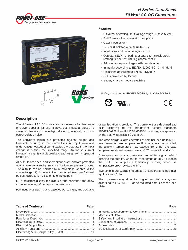
® H Series Data Sheet 70 Watt AC-DC Converters BCD20019 Rev AB Page 1 of 21 www.power-one.com Description The H Series of AC-DC converters represents a flexible range of power supplies for use in advanced industrial electronic systems. Features include high efficiency, reliability, and low output voltage noise. The converter inputs are protected against surges and transients occuring at the source lines. An input over- and undervoltage lockout circuit disables the outputs, if the input voltage is outside the specified range. An inrush current limitation prevents circuit breakers and fuses from tripping at switch-on. All outputs are open- and short-circuit proof, and are protected against overvoltages by means of built-in suppressor diodes. The outputs can be inhibited by a logic signal applied to the connector (pin 2). If the inhibit function is not used, pin 2 should be connected to pin 23 to enable the outputs. LED indicators display the status of the converter and allow visual monitoring of the system at any time. Full input to output, input to case, output to case, and output to output isolation is provided. The converters are designed and built according to the international safety standards IEC/EN 60950-1 and UL/CSA 60950-1, and they are approved by the safety agencies TÜV and UL. The case design allows operation at nominal load up to 50 °C in a free-air ambient temperature. If forced cooling is provided, the ambient temperature may exceed 50 °C but the case temperature should remain below 80 °C under all conditions. A temperature sensor generates an inhibit signal, which disables the outputs, when the case temperature T C exceeds the limit. The outputs automatically recover, when the temperature drops below the limit. Two options are available to adapt the converters to individual applications (D, V). The converters may either be plugged into 19" rack system according to IEC 60927-3 or be mounted onto a chassis or a plate. Features • Universal operating input voltage range 85 to 255 VAC • RoHS lead-solder exemption compliant • Class I equipment • 1, 2, or 3 isolated outputs up to 64 V • Input over- and undervoltage lockout • Outputs: SELV, no load, overload, short-circuit proof, rectangular current limiting characteristic • Adjustable output voltages with remote on/off • Immunity according to IEC/EN 61000-4-2, -3, -4, -5, -6 • Emissions according to EN 55011/55022 • PCBs protected by lacquer • Battery charger models available Table of Contents Page Page 168 6.6" 39 1.54" 8TE 111 4.37" 3U Safety according to IEC/EN 60950-1, UL/CSA 60950-1 Description ............................................................................ 1 Model Selection .................................................................... 2 Functional Description .......................................................... 3 Electrical Input Data .............................................................. 4 Electrical Output Data ........................................................... 5 Auxiliary Functions ................................................................ 9 Electromagnetic Compatibility (EMC) ................................. 11 Immunity to Environmental Conditions ............................... 12 Mechanical Data ................................................................. 13 Safety and Installation Instructions ..................................... 14 Description of Options ........................................................ 15 Accessories ......................................................................... 20 EC Declaration of Conformity ............................................. 21
Transcript
®
H Series Data Sheet70 Watt AC-DC Converters
BCD20019 Rev AB Page 1 of 21 www.power-one.com
DescriptionThe H Series of AC-DC converters represents a flexible rangeof power supplies for use in advanced industrial electronicsystems. Features include high efficiency, reliability, and lowoutput voltage noise.
The converter inputs are protected against surges andtransients occuring at the source lines. An input over- andundervoltage lockout circuit disables the outputs, if the inputvoltage is outside the specified range. An inrush currentlimitation prevents circuit breakers and fuses from tripping atswitch-on.
All outputs are open- and short-circuit proof, and are protectedagainst overvoltages by means of built-in suppressor diodes.The outputs can be inhibited by a logic signal applied to theconnector (pin 2). If the inhibit function is not used, pin 2 shouldbe connected to pin 23 to enable the outputs.
LED indicators display the status of the converter and allowvisual monitoring of the system at any time.
Full input to output, input to case, output to case, and output to
output isolation is provided. The converters are designed andbuilt according to the international safety standardsIEC/EN 60950-1 and UL/CSA 60950-1, and they are approvedby the safety agencies TÜV and UL.
The case design allows operation at nominal load up to 50 °Cin a free-air ambient temperature. If forced cooling is provided,the ambient temperature may exceed 50 °C but the casetemperature should remain below 80 °C under all conditions.
A temperature sensor generates an inhibit signal, whichdisables the outputs, when the case temperature TC exceedsthe limit. The outputs automatically recover, when thetemperature drops below the limit.
Two options are available to adapt the converters to individualapplications (D, V).
The converters may either be plugged into 19" rack systemaccording to IEC 60927-3 or be mounted onto a chassis or aplate.
Features• Universal operating input voltage range 85 to 255 VAC• RoHS lead-solder exemption compliant• Class I equipment• 1, 2, or 3 isolated outputs up to 64 V• Input over- and undervoltage lockout• Outputs: SELV, no load, overload, short-circuit proof,
rectangular current limiting characteristic• Adjustable output voltages with remote on/off• Immunity according to IEC/EN 61000-4-2, -3, -4, -5, -6• Emissions according to EN 55011/55022• PCBs protected by lacquer• Battery charger models available
Table of Contents Page Page
168
6.6"39
1.54"
8TE
111
4.37"
3U
Safety according to IEC/EN 60950-1, UL/CSA 60950-1
Immunity to Environmental Conditions ............................... 12Mechanical Data ................................................................. 13Safety and Installation Instructions ..................................... 14Description of Options ........................................................ 15Accessories ......................................................................... 20EC Declaration of Conformity ............................................. 21
®
H Series Data Sheet70 Watt AC-DC Converters
BCD20019 Rev AB Page 2 of 21 www.power-one.com
Model SelectionNon-standard input/output configurations or special customadaptions are available on request. Table 1 provides anoverview of the basic input and output configurations. More
Table 1a: Standard models
Output 1 Output 2 Output 3 Operating input voltage range and efficiency 1 Options 2
Vo nom Io nom Vo nom Io nom V nom Io nom Vi min – Vi max ηηηηηmin[VDC] [A] [VDC] [A] [VDC] [A] 85 – 255 VAC, 47 – 63 Hz [%]
than 1000 different types have been manufactured withdifferent input /output configurations and customizedspecialities. Please consult Power-One for additionalinformation.
Table 1b: Battey charger models
Output Operating input voltage range and efficiency 1 Options 2
VBat V o safe 3 Vo max Io nom Vi min – Vi max ηηηηηmin[VDC] [VDC] [VDC] [A] 85 – 255 VAC, 47 – 63 Hz [%]
1 Min. efficiency at Vi nom and Io nom. Typical values are approx. 2% better.2 Ask Power-One for availability!3 Setting voltage with open R-input (battery chargers)
®
H Series Data Sheet70 Watt AC-DC Converters
BCD20019 Rev AB Page 3 of 21 www.power-one.com
Part Number Description L H 1 5 01 -2 R D3
Operating input range Vi:85 – 255 VAC, 47 – 63 Hz ................... L
Series ................................................................................... HNumber of outputs ........................................................ 1, 2, 3Output 1, Vo1 nom: 5.1 V ............ 0, 1, 2
12 V .................... 315 V ................ 4, 524 V .................... 6
other voltages ................ 7, 848 V .................... 9
5.1 V ....................................................................01 – 1912 V .....................................................................20 – 3915 V .....................................................................40 – 5924 V .....................................................................60 – 69other voltages for multiple-output models ...........70 – 99
Ambient temperature range TA:–10 to 50 °C .................. -2
customer-specific .................. -0Auxiliary functions and options:
Output voltage control input (single-output models) .... RSave data signal (D1 – D8, to be specified) ................ D 1
ACFAIL signal (V2, V3, to be specified) ....................... V 1
1 Option D excludes option V and vice versa
Example: LH1501-2D3: AC-DC converter,operating input voltage range 85 – 255 VAC, providing one output with 15 V /4.5 A, equipped with an output voltage adjust input (R), and undervoltage monitor D3.
Functional DescriptionThe input voltage is fed via an input fuse, an input filter, and aninrush current limiter to the input capacitor. This capacitorsources a single-transistor forward converter. Each output ispowered by a separate secondary winding of the maintransformer. The resultant voltages are rectified and theirripples smoothed by a power choke and an output capacitor.The main control circuit senses the main output voltage Vo1and generates, with respect to the maximum admissible outputcurrents, the control signal for the primary switching transistor.This signal is transferred to the primary side by a couplingtransformer.
The auxiliary output voltages Vo2 and Vo3 are tracking. Eachauxiliary output's current is sensed using a currenttransformer. If one of the outputs is driven into current limit, theother outputs will reduce their output voltages as well, becauseall output currents are controlled by the same main controlcircuit.
®
H Series Data Sheet70 Watt AC-DC Converters
BCD20019 Rev AB Page 4 of 21 www.power-one.com
Fig. 1
Block diagram of a triple-output model.
Inpu
t filt
er
Current limitationoutput 3
Main control circuit
Currentlimitationoutput 2
29
11
8
23
5
26
32
17
14
20
2
For
war
d co
nver
ter
appr
ox. 7
0 kH
z
4
4
CY
CY
14
17
i
D, V
R
G
N
L
2
3
03084a
1
1 Input fuse2 Transient suppressor3 Inrush current limiter (NTC)4 Adjust input for single-output models with feature R.
Electrical Input DataGeneral conditions:– TA = 25 °C, unless TC is specified.– Connector pins 2 and 23 interconnected, R input not connected; with option P: Vo = Vo nom
Table 2: Input data
Input LM Unit
Characteristics Conditions min typ max
Vi Operating input voltage Io = 0 – Io nom 85 255 VAC1
Vi nom Nominal input voltage TC min – TC max 230
I i Input current Vi nom, Io = Io nom 2 0.44 A
Pi 0 No-load input power: Vi nomSingle-output model Io1,2,3 = 0 1 2.5 WDouble-output model 7 9Triple-output model 7 9
Pi inh Idle input power inhibit mode 2.5
Iinr p 5 Peak inrush current Vi = Vi max 42 4 A
t inr r Rise time RS = 0 Ω 3300 µs
t inr h Time to half-valueTC = 25 °C
1600
R i Input resistance TC = 25 °C 800 mΩ
RNTC NTC resistance 8000 4
Ci Input capacitance 140 270 µF
Vi abs Input voltage limits 0 284 VACwithout any damage
1 Frequency 47 – 63 Hz2 With multiple-output models, the same
condition for each output applies.3 RS = source resistance.4 Value for initial switch-on cycle.5 I inr p = Vi / (Rs + R i + RNTC ); see Inrush
Current.
®
H Series Data Sheet70 Watt AC-DC Converters
BCD20019 Rev AB Page 5 of 21 www.power-one.com
Input FuseA slow-blow fuse (Schurter SPT 2.5 A, 250 V, size 5 × 20 mm)mounted inside of the converter protects against severedefects. The fuse is not accessible by the user.
The fuse and a VDR form together with the input filter aneffective protection against high input transients.
Input Under-/Overvoltage LockoutIf the input voltage is below approx. 60 VAC or exceedsapprox. 280 VAC, an internally generated inhibit signaldisables the output(s). When checking this function theabsolute maximum input voltage rating Vi abs must be carefullyconsidered (see table Input data).
Note: When Vi is between Vi min and the undervoltage lockoutlevel, the output voltage may be below the value defined in tableOutput data.
Inrush CurrentThe converters incorporate an NTC resistor in the input line,which at initial switch-on cycle limits the peak inrush current, in
Rs Ri RNTCIinr p
Vi rms Ci
04001a
order to prevent the connectors and switching devices fromdamage. Subsequent switch-on cycles within a short intervalwill cause an increase of the peak inrush current due to thewarming-up of the NTC resistor.
The inrush current at switch-on can be calculated as follows:
Iinr p = √
–2 • Vi rms / (Rs + R i + RNTC)
Fig. 2Equivalent circuit diagram for input impedance
Electrical Output DataGeneral conditions– TA = 25 °C, unless TC is specified.– Connector pins 2 and 23 interconnected, R input not connected.
Table 3a: Output data of single-output models
Output Vo nom 5.1 V 12 V 15 V 24 V 48 V Unit
Characteristics Conditions min typ max min typ max min typ max min typ max min typ max
Vo Output voltage Vi nom, Io nom 5.0 5.20 11.76 12.24 14.70 15.30 23.52 24.48 47.04 48.96 V
Vo p Output overvoltage 7.5 21 25 41 85protection 1
Io nom Output current Vi min – Vi max 0 11 0 6 0 4.5 0 3 0 1.5 A
Io L Output current TC min – TC max 11.44 6.24 4.68 3.12 1.56limit
vo Output Switch. freq. V i nom, Io nom 30 50 60 100 50 80 50 80 50 100 mVppvoltage Total IEC/EN 61204 60 120 40 80 40 80 40 80 -noise BW = 20 MHz
∆Vo V Static line regulation Vi min – Vi nom ±50 ±100 ±100 ±150 ±150 mVVi nom – Vi maxIo nom
∆Vo I Static load regulation Vi nom, Io nom – 0 50 150 150 150 150
vo d Dynamic Voltage Vi nom ±220 ±400 ±200 ±200 ±150load deviation Io nom ↔ 1/3 Io nom
tdregulation2
Recovery IEC/EN 61204 100 80 80 80 120 µstime
αVo Temperature Vi min – Vi max ±0.02 ±0.02 ±0.02 ±0.02 ±0.02 %/Kcoefficient 0 – Io nom ±1.0 ±2.4 ±3.0 ±4.8 ±9.6 mV/K∆Vo /∆TC
1 By suppressor diode2 See fig. 4 Dynamic load regulation.
®
H Series Data Sheet70 Watt AC-DC Converters
BCD20019 Rev AB Page 6 of 21 www.power-one.com
Table 3b: Output data of double-output models. Same general conditions as per table 3a
Output Vo nom 2 × 12 V 2 × 15 V Unit
Output 1 Output 2 Output 1 Output 2Characteristics Conditions min typ max min typ max min typ max min typ max
Vo Output voltage Vi nom, Io nom 11.76 12.24 11.4 12.6 14.7 15.3 14.25 15.75 V
Vi nom, Io2 = 0 13.8 17.25
Vo p Output overvoltage 21 25 25 31protection
Io nom Output current Vi min – Vi max 0 2 0 2 0 1.7 0 1.7 A
Io L Output current limit TC min – TC max 2.08 2.08 1.77 1.77
vo Output Switch. freq. V i nom, Io nom 15 30 20 40 15 30 20 40 mVppvoltage IEC/EN 61204 50 150 50 150 40 150 40 150noise 1 Total BW = 20 MHz
∆Vo V Static line regulation Vi min – Vi nom ±50 ±80 ±60 ±180 mVVi nom – Vi maxIo nom
∆Vo I Static load regulation Vi nom, Io nom – 0 3 50 2 60 2
αVo Temperature Vi min – Vi max ±2.4 ±3.0 mV/Kcoefficient ∆Vo /∆TC 0 – Io nom
Table 3c: Output data of triple-output models. Same general conditions as per table 3a
Output Vo nom 5.1 V, 2 × 12 V 5.1 V, 2 × 15 V Unit
Output 1 Output 2 Output 1 Output 2Characteristics Conditions min typ max min typ max min typ max min typ max
Vo Output voltage Vi nom, Io nom 5.0 5.2 11.4 12.6 5.0 5.2 14.25 15.75 V
Vi nom, Io2 = Io3 = 0 13.8 17.25
Vo p Output overvoltage 7.5 25 7.5 31protection
Io nom Output current Vi min – Vi max 0 5 0 0.7 0 5 0 0.6 A
Io L Output current limit TC min – TC max 5.2 0.73 5.2 0.62
vo Output Switch. freq. V i nom, Io nom 15 30 10 20 15 30 10 20 mVppvoltage IEC/EN 61204 30 150 50 150 40 150 40 150noise 1 Total BW = 20 MHz
∆Vo V Static line regulation Vi min – Vi nom ±30 ±150 ±30 ±150 mVVi nom – Vi maxIo nom
∆Vo I Static load regulation Vi nom, Io nom – 0 3 25 2 250 2
αVo Temperature Vi min – Vi max ±1.0 ±1.0 mV/Kcoefficient ∆Vo /∆TC 0 – Io nom
1 Measured with a clamp according to IEC 612042 See Voltage regulation of tracking outputs3 Condition for the specified output; other outputs loaded with Io nom
®
H Series Data Sheet70 Watt AC-DC Converters
BCD20019 Rev AB Page 7 of 21 www.power-one.com
Io1/Io1 nom
1
Vo1d
td td
∆Vo1 I ∆Vo1 I
t
Vo1
0 t≥10 µs≥10 µs
05131a
0.5
Vo1d
13
14
15
16
17
0.2 0.4 0.60
05134aVo2, Vo3 [V]
Io2 = Io3 [A]0.8
Io1 = 5 A Io1 = 2.5 A Io1 = 0.25 A
14.0
14.5
15.0
16.0
16.5
0.4 0.8 1.60
Io1 = 1.7 A Io1 = 0.85 A
Vo2 [V]
Io2 [A]
05135a
Io1 = 0.08 A
1.2 2.0
15.5
11.0
11.5
12.0
12.5
13.0
13.5
0.2 0.4 0.6 0.8 0
Io1 = 5 A Io1 = 2.5 A Io1 = 0.25 A
Vo2, Vo3 [V]05132a
Io2 = Io3 [A]
Io1 = 0.1 A
11.0
11.5
12.0
12.5
13.0
13.5
0.2 0.6 1.0 1.4
Io1 = 2 A Io1 = 1 A
Vo2 [V]
Io2 [A]1.8 2.2
05133a
Fig. 3Typical main output voltage Vo1 versus current Io1
Fig.4Dynamic load regulation of Vo1 versus load change.
1.0
0
0.5
Vo
0.5
Vo nom
Io
Io nom1.0 1.2
Io nom
Io1
Io2,Io3
IoL1
IoL2, IoL3
0.95
05022a
Output Characteristic and ProtectionEach output is protected by a suppressor diode, which under aworst case condition may become a short circuit. Thesuppressor diodes are not designed to withstand externallyapplied overvoltages. Overload at any of the outputs will causea shutdown of all outputs. A red LED indicates the overloadcondition of the respective output.
Regulation of Multiple-Output ModelsOutput 1 is under normal conditions regulated to Vo1 nom,
Fig. 5Static load regulation Vo2 versus Io1 (LH2320-2)
regardless of the output current. The voltage of the trackingoutputs 2 and 3 depends upon their load and the load onoutput 1; see fig. 5 to 8.
Fig. 6Static load regulation Vo2 versus Io1 (LH2540-2)
Fig. 7Static load regulation Vo2 and Vo3 versus Io1 (LH3020-2,Io2 = Io3)
Fig. 8Static load regulation Vo2 and Vo3 versus Io1 (LH3040-2,Io2 = Io3)
®
H Series Data Sheet70 Watt AC-DC Converters
BCD20019 Rev AB Page 8 of 21 www.power-one.com
0
0.2
0.4
0.6
0.8
40 60 70 80
Io/Io nom
TA [°C]
1.0Forced cooling
05142a
TC max
50
Convection cooling
LH2000LH3000
LH1000
Fig. 9Output current derating versus temperature
Thermal Considerations and ProtectionIf a converter is located in free, quasi-stationary air (convectioncooling) at the indicated maximum ambient temperature TA max(see table Temperature specifications) and is operated at itsnominal input voltage and output power, the temperaturemeasured at the measuring point of case temperature TC (seeMechanical Data) will approach the indicated value TC max afterthe warm-up phase. However, the relationship between TA andTC depends heavily on the conditions of operation andintegration into a system. The thermal conditions areinfluenced by input voltage, output current, airflow, andtemperature of surrounding components and surfaces. TA maxis therefore, contrary to TC max, an indicative value only.
Caution: The installer must ensure that under all operatingconditions TC remains within the limits stated in the tableTemperature specifications.
Notes: Sufficient forced cooling or an additional heat sink allow TAto pass over 50 °C, if TC max is not exceeded.
At an ambient temperature TA of 65 °C with only convectioncooling, the maximum permissible current for each output isapprox. 50% of its nominal value; see fig. 9 .
A temperature sensor generates an internal inhibit signaldisabling the outputs, when the case temperature exceedsTC max. The outputs automatically recover, when thetemperature drops below this limit.
Parallel and Series ConnectionMain outputs of equal nominal voltage can be connected inparallel. It is important to assure that the main output of amultiple-output converter is forced to supply a minimumcurrent of 10% of Io nom to enable correct operation of its ownauxiliary outputs.
In parallel operation, one or more of the main outputs mayoperate continuously in current limitation, causing an increase
of the case temperature TC. Consequently, a reduction of themax. ambient temperature by 10 K is recommended.
Both outputs of a double-output converter may be connectedin parallel without any restriction.
Note: If output 2 of a double-output converter is not used, werecommend to connect it in parallel with the main output.
Output 2 and output 3 of a triple-output converter may beconnected in parallel without any restriction.
Note: If the output 2 or 3 of a triple-output converter is not used, werecommend to connect it in parallel with the other auxiliary output.
Main or auxiliary outputs can be connected in series with anyother output of the same or another converter. In seriesconnection, the maximum output current is limited by thelowest current limit. Output ripple and regulation values areadded. Connection wiring should be kept as short as possible.
If output terminals are connected together in order to establishmulti-voltage configurations, e.g., +5.1 V, ±12 V etc., thecommon-ground connecting point should be as close aspossible to the connector of the converter in order to avoidexcessive output ripple voltages.
Auxiliary outputs of different converters should not beconnected in parallel!
®
H Series Data Sheet70 Watt AC-DC Converters
BCD20019 Rev AB Page 9 of 21 www.power-one.com
1.6
0.8
0
–0.8–50
Vinh [V]
Iinh [mA]
–30 0–10 10 30 50
2.0
1.2
0.4
–0.4
Vinh = 0.8 V
Vo = on Vo = off
Vinh = 2.4 V
06032a
Vo–
i
Vo+Iinh
Vinh
06115a
N
L
Table 5: Output response time tr and tf (see fig. 4). Values not applicable for models equipped with option E.
Type of converter t r at Po = 0 and t f at Po = Po nom tr and t f at Po = 3/4 Po nom t r at Po = Po nom Unittyp max typ max typ max
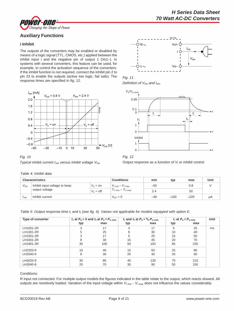
i InhibitThe outputs of the converters may be enabled or disabled bymeans of a logic signal (TTL, CMOS, etc.) applied between theinhibit input i and the negative pin of output 1 (Vo1–). Insystems with several converters, this feature can be used, forexample, to control the activation sequence of the converters.If the inhibit function is not required, connect the inhibit pin 2 topin 23 to enable the outputs (active low logic, fail safe). Theresponse times are specified in fig. 12.
Fig. 11Definition of Vinh and Iinh.
Fig. 10Typical inhibit current I inh versus inhibit voltage Vinh
Table 4: Inhibit data
Characteristics Conditions min typ max Unit
Vinh Inhibit input voltage to keep Vo = on Vi min – V i max –50 0.8 Voutput voltage Vo = off TC min – TC max 2.4 50
I inh Inhibit current Vinh = 0 –60 –100 –220 µA
0 tr tft
t0
Inhibit
1
Vo/Vo nom
0.1
t0
1
0.95
thVi
05025a
Fig. 12Output response as a function of Vi or inhibit control
Conditions:R input not connected. For multiple-output models the figures indicated in the table relate to the output, which reacts slowest. Alloutputs are resistively loaded. Variation of the input voltage within Vi min – Vi max does not influence the values considerably.
®
H Series Data Sheet70 Watt AC-DC Converters
BCD20019 Rev AB Page 10 of 21 www.power-one.com
Table 6a: Rext1 for Vo < Vo nom (conditions: Vi nom, Io nom, rounded up to resistor values E 96, Rext2 is not fitted )
Vo nom = 5.1 V Vo nom = 12 V Vo nom = 15 V Vo nom = 24 V Vo nom = 48 VVo [V] Rext1 [kΩΩΩΩΩ] Vo [V] Rext1 [kΩΩΩΩΩ] Vo [V] Rext1 [kΩΩΩΩΩ] Vo [V] Rext1 [kΩΩΩΩΩ] Vo [V] Rext1 [kΩΩΩΩΩ]
Table 6b: R2 for Vo > Vo nom (conditions: Vi nom, Io nom, rounded up to resistor values E 96, Rext1 is not fitted )
Vo nom = 5.1 V Vo nom = 12 V Vo nom = 15 V Vo nom = 24 V Vo nom = 48 VVo [V] Rext2 [kΩΩΩΩΩ] Vo [V] Rext2 [kΩΩΩΩΩ] Vo [V] Rext2 [kΩΩΩΩΩ] Vo [V] Rext2 [kΩΩΩΩΩ] Vo [V] Rext2 [kΩΩΩΩΩ]
R Output Voltage AdjustmentAs a standard feature, single-output models offer anadjustable output voltage identified by letter R in the typedesignation.
Note: With open R input, Vo = Vo nom.
The output voltage Vo can either be adjusted by an externalvoltage (Vext) or by an external resistor (Rext1 or Rext2). Theadjustment range is approximative 0 – 110% of Vo nom. Foroutput voltages Vo > Vo nom, the minimum input voltage Vi minspecified in Electrical Input Data increases proportionally toVo/Vo nom.
Fig. 13Output voltage adjustment
a) Adjustment by means of an external resistor Rext:Depending upon the value of the required output voltage,the resistor shall be connected:either: Between the R and G pin to achieve an outputvoltage adjustment range of Vo ≈ 0 to 100% of Vo nom.
VoRext1 ≈ 4 kΩ • ––––––––– Vo nom – Vo
or: Between the R pin and Vo+ to achieve an outputvoltage range of Vo ≈ 100 to 110% of Vo nom.
(Vo – 2.5 V)Rext2 ≈ 4 kΩ • –––––––––––––––––– 2.5 V • (Vo/Vo nom – 1)
Caution: To prevent damage, Rext2 should never be less than47 kΩ.
Note: R inputs of n converters with paralleled outputs may beparalleled too, but if only one external resistor is used, itsvalue should be Rext1 /n or Rext2 /n respectively.
b) Adjustment by means of an external control voltage Vextbetween G and R pin:The control voltage range is 0 to 2.75 V and allows foradjustment in the range of Vo ≈ 0 to 110% of Vo nom.
Vo • 2.5 VVext ≈ –––––––– Vo nom
Caution: The external control voltage should be in the range0 to +3 V to prevent the converter from damage.
R
Vo+
G
+
Vext
-
4 kΩVref = 2.5 V
Control
logicRext1
Rext2
06087a
Vi–
Vi+
17
14
+
8
®
H Series Data Sheet70 Watt AC-DC Converters
BCD20019 Rev AB Page 11 of 21 www.power-one.com
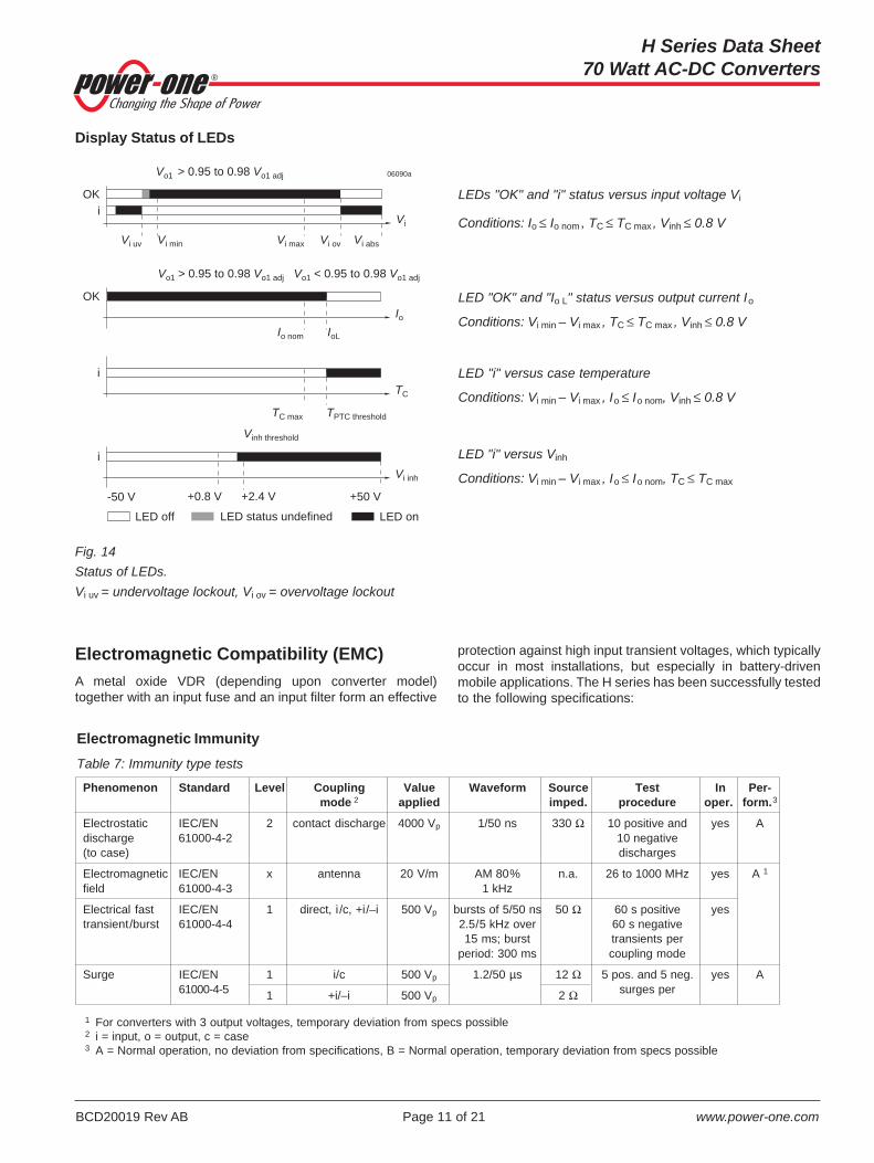
Display Status of LEDs
LEDs "OK" and "i" status versus input voltage Vi
Conditions: Io ≤ Io nom , TC ≤ TC max , Vinh ≤ 0.8 V
LED "OK" and "Io L" status versus output current Io
Conditions: Vi min – Vi max , TC ≤ TC max , Vinh ≤ 0.8 V
LED "i" versus case temperature
Conditions: Vi min – Vi max , Io ≤ Io nom, Vinh ≤ 0.8 V
LED "i" versus Vinh
Conditions: Vi min – Vi max , Io ≤ Io nom, TC ≤ TC max
Fig. 14Status of LEDs.Vi uv = undervoltage lockout, Vi ov = overvoltage lockout
Vo1 > 0.95 to 0.98 Vo1 adj
Vi max Vi ovVi minVi uv
Vi
Vi abs
OK
i
Vo1 > 0.95 to 0.98 Vo1 adj
Io nom IoL
Io
OK
Vo1 < 0.95 to 0.98 Vo1 adj
TC
i
TC max TPTC threshold
Vi inh
i
+50 V+0.8 V +2.4 V-50 V
Vinh threshold
LED off LED onLED status undefined
06090a
Electromagnetic ImmunityTable 7: Immunity type tests
Phenomenon Standard Level Coupling Value Waveform Source Test In Per-mode 2 applied imped. procedure oper. form. 3
1 For converters with 3 output voltages, temporary deviation from specs possible2 i = input, o = output, c = case3 A = Normal operation, no deviation from specifications, B = Normal operation, temporary deviation from specs possible
Electromagnetic Compatibility (EMC)A metal oxide VDR (depending upon converter model)together with an input fuse and an input filter form an effective
protection against high input transient voltages, which typicallyoccur in most installations, but especially in battery-drivenmobile applications. The H series has been successfully testedto the following specifications:
®
H Series Data Sheet70 Watt AC-DC Converters
BCD20019 Rev AB Page 12 of 21 www.power-one.com
Electromagnetic Emissions
Table 8: Emissions at Vi nom and Io nom
Series IEC/EN 55022
≤ 30 MHz ≥30 MHz
LH <A <B
Table 10: Temperature specifications, values given are for an air pressure of 800 – 1200 hPa (800 – 1200 mbar)
Temperature Standard -2
Characteristics Conditions min max Unit
TA Ambient temperature Operational –10 50 1 °C
TC Case temperature –10 80
TS Storage temperature Not operational –25 100
1 Single output models up to 71 °C with derating.
Immunity to Environmental ConditionsTable 9: Mechanical and climatic stress
Test method Standard Test conditions Status
Cab Damp heat IEC/EN 60068-2-78 Temperature: 40 ±2 °C Convertersteady state MIL-STD-810D section 507.2 Relative humidity: 93 +2/-3 % not
Duration: 21 days operating
Ea Shock IEC/EN 60068-2-27 Acceleration amplitude: 15 gn = 147 m/s2 Converter(half-sinusoidal) MIL-STD-810D section 516.3 Bump duration: 6 ms operating
Number of bumps: 18 (3 each direction)
Eb Bump IEC/EN 60068-2-29 Acceleration amplitude: 10 gn = 98 m/s2 Converter(half-sinusoidal) MIL-STD-810D section 516.3 Bump duration: 16 ms operating
Number of bumps: 6000 (1000 each direction)
Fc Vibration IEC/EN/DIN EN 60068-2-6 Acceleration amplitude: 0.15 mm (10 – 60 Hz) Converter(sinusoidal) MIL-STD-810D section 514.3 2 gn = 20 m/s2 (60 – 150 Hz) operating
Frequency (1 Oct/min): 10 – 150 HzTest duration: 3.75 h (1.25 h each axis)
Table 11: MTBF
Values at specified Model Ground benign UnitCase Temperature 40 °C
Fig. 15Case H02, weight approx. 770 g,Aluminium, black finish
®
H Series Data Sheet70 Watt AC-DC Converters
BCD20019 Rev AB Page 14 of 21 www.power-one.com
Safety and Installation Instructions
Connector Pin AllocationPin no. 26 (protective earth) is leading, ensuring that it makescontact with the female connector first.
Table 12: Pin allocationFig. 16View of male H11 connector.
Installation InstructionsThe H Series converters are components, intended exclusivelyfor inclusion within other equipment by professional installers.Installation must strictly follow the national safety regulationsin compliance with the enclosure, mounting, creepage,clearance, casualty, markings and segregation requirementsof the end-use application.
Connection to the system shall be made via the femaleconnector H11. Other installation methods may not meet thesafety requirements.
The converters are provided with pin no. 26 ( ), which isreliably connected with the case. For safety reasons, it isessential to connect this pin with the protective earth of thesupply system.
A non-accessible input fuse is connected in the line to pin 32(L ). Since this fuse is designed to protect the converter incase of an overcurrent and does not necessarily cover allcustomer needs, an external fuse suitable for the applicationand in compliance with the local requirements may benecessary in the wiring to one or both input pins (no. 29 and/orno. 32), particularily if the phase or neutral line cannot beassigned to the corresponding terminals.
Important: If the inhibit function is not in use, pin 2 (i) should beconnected with pin 23 (Vo–) to enable the output(s).
Caution: Do not open the converters, or warranty will beinvalidated.
Make sure that there is sufficient air flow possiblefor convection cooling. This should be verified bymeasuring the case temperature TC, when theconverter is installed and operated in the end-useapplication. The maximum specified casetemperature TC max shall not be exceeded. See alsoThermal Considerations.
Cleaning AgentsIn order to avoid possible damage, any penetrationof liquids (e.g., cleaning fluids) has to be prevented,since the power supplies are not hermeticallysealed.
Note: All boards are coated with a protection lacquer.
Protection DegreeCondition: Female connector fitted to the converter.
• IP 40: All models, except those with options D or V with apotentiometer.
• IP 20: All models other models.
Standards and ApprovalsThe converters correspond to class I equipment and havebeen approved according to the standards IEC/EN 60950-1and UL/CSA 60950-1.
The converters have been evaluated for:• Class I equipment• Building in• Basic insulation between input and case and double or
reinforced insulation between input and output, based onthe input voltage of 250 VAC or 400 VDC
• Functional insulation between output(s) and case• Functional insulation between the outputs• Pollution degree 2 environment• Overvoltage catagory II• Altitude up to 2000 m
The converters are subject to manufacturing surveillance inaccordance with the above mentioned standards and with ISO9001:2000.
IsolationThe electric strength test is performed in the factory as routinetest in accordance with EN 50116 and IEC/EN 60950, andshould not be repeated in the field. Power-One will not honorany warranty claims resulting from electric strength field tests.
1 Not connected, if option neither option D or V is fitted.2 Leading pin
Inhibit 2 i 2 i 2 iSafe Data or ACFAIL 5 D or V 1 5 D or V 1 5 D or V 1
Output voltage (positive) 8 Vo+ 8 n.c. 8 Vo3+Output voltage (negative) 11 Vo– 11 n.c. 11 Vo3–
Voltage adjust 14 RAdjust return 17 G
Output voltage (positive) 14 Vo2+ 14 Vo2+Output voltage (negative) 17 Vo2– 17 Vo2–
Output voltage (positive) 20 Vo+ 20 Vo1+ 20 Vo1+Output voltage (negative) 23 Vo– 23 Vo1– 23 Vo1–
Protective earthing PE 2 26 26 26
AC neutral input 29 N 29 N 29 NAC line input 32 L 32 L 32 L
®
H Series Data Sheet70 Watt AC-DC Converters
BCD20019 Rev AB Page 15 of 21 www.power-one.com
Safety of Operator-Accessible Output CircuitsIf the output circuit of a DC-DC converter is operator-accessible, it shall be an SELV circuit according to the safetystandard IEC/EN 60950.
The table below shows a possible configuration, compliancewith which causes the output to be an SELV circuit up to aconfigured output voltage of 36 V (sum of the nominal voltagesconnected in series).
Fig. 17Schematic safety concept.
Table 12: Isolation
Characteristic Input to case Output(s) to Output to Unitand output(s) case output
Electric Factory test >1 s 2.8 1 1.4 0.3 kVDCstrength AC test voltage equivalent 2.0 1.0 0.2 kVACtest to factory testInsulation resistance at 500 VDC >300 >300 >100 2 MΩ1 According to EN 50116 and IEC/EN 60950, subassemblies connecting input to output are pre-tested with 5.6 kVDC or 4 kVAC.2 Tested at 300 VDC
AC-DCcon-
verter
Mains SELV
Earth connection
+
–
~~
10021a
Fuse
Fuse
Table 13: Safety concept leading to an SELV output circuit
Conditions AC-DC converter Installation Result
Nominal Supply Grade of insulation between Measures to achieve the resulting Safety statuts of the AC-DCvoltage input and output, provided safety statuts of the output circuit converter output circuit
by the AC-DC converter
Mains ≤250 V AC Double or reinforced Earthed case 1 and installation SELV circuitaccording to the applicable standards
1 The earth connection has to be provided by the installer according to the relevant safety standards, e.g. IEC/EN 60950
Description of Options
D Undervoltage MonitorThe input and/or output undervoltage monitoring circuitoperates independently of the built-in input undervoltagelockout circuit. A logic "low" (JFET output) or "high" signal(NPN output) is generated at pin 5, as soon as one of themonitored voltages drops below the preselected threshold
Table 14: Survey of options
Option Function of Option Characteristic
D Input and/or output undervoltage monitoring circuitry Safe data signal output (D1 – D8)
V 1 Input and output undervoltage monitoring circuitry ACFAIL signal according to VME specifications ( V2, V3)
1 Option V is only available for models with 5.1 V main output; it excludes option D.
level V t. The return for this signal is Vo1– (pin 23). The D outputrecovers, when the monitored voltages exceeds Vt + Vh. Thethreshold level Vt is adjustable by a potentiometer, accessiblethrough a hole in the front cover.
Option D exists in various versions D1 – D8 as shown in table15.
Table 15: Undervoltage monitor functions
Output type Monitoring Minimum adjustment range Typical hysteresis Vh [% of Vt]JFET NPN Vi Vo1 of threshold level Vt for Vt min – Vt max
Vti Vto Vhi Vho
D1 D5 no yes – 3.5 V – 48 V 1 – 2.3 – 1
D2 D6 yes no Vi min – Vi max 1 – 3.0 – 0.5 –
D3 D7 yes yes Vi min – Vi max 1 0.95 – 0.98 Vo1 2 3.0 – 0.5 "0"
D4 D8 no yes – 0.95 – 0.98 Vo1 2 – "0"1 Threshold level adjustable by potentiometer (not recommended for mobile applications)2 Fixed value between 95% and 98% of Vo1 (tracking)
®
H Series Data Sheet70 Watt AC-DC Converters
BCD20019 Rev AB Page 16 of 21 www.power-one.com
JFET output (D1 – D4):
Connector pin D is internally connected via the drain-sourcepath of a JFET (self-conducting type) to the negative potentialof output 1. VD – 0.4 V (logic low) corresponds to a monitoredvoltage level (Vi and/or Vo1) < Vt. The current I D through theJFET should not exceed 2.5 mA. The JFET is protected by a0.5 W Zener diode of 8.2 V against external overvoltages.
Vi, Vo1 status D output, VD
Vi or Vo1 < Vt low, L, VD – 0.4 V at I D = 2.5 mA
Vi and Vo1 > Vt + Vh high, H, ID – 25 µA at VD = 5.25 V
NPN output (D5 – D8):
Connector pin D is internally connected via the collector-emitter path of a NPN transistor to the negative potential ofoutput 1. VD – 0.4 V (logic low) corresponds to a monitoredvoltage level (Vi and/or Vo1) > Vt + Vh. The current ID through
Vi, Vo1 status D output, VD
Vi or Vo1 < Vt high, H, ID – 25 µA at VD = 40 V
Vi and Vo1 > Vt + Vh low, L, VD – 0.4 V at ID = 20 mA
Fig. 18Options D1 – D4, JFET output
Fig. 19Options D5 – D8, NPN output
Vo1+
Vo1–
D
VD
ID
Rp
Input
11006
Vo1+
Vo1–
D
VD
ID
Rp
Inp
ut
11007a
Threshold tolerances and hysteresis:
If V i is monitored, the internal input voltage after the input filterand rectifier is measured. Consequently, this voltage differsfrom the voltage at the connector pins by the voltage drop ∆Vtiacross input filter and rectifier. The threshold level of the D1and D8 options is adjusted in the factory at nominal outputcurrent Io nom and TA = 25 °C.
Fig. 20Definition of Vti, ∆Vti, and Vhi (JFET output)
∆Vti Vhi
VD low
VD
VD high
Vi
Po =
Po n
om
Po =
0
Po =
0
Vti
Po =
Po n
om
11021a
®
H Series Data Sheet70 Watt AC-DC Converters
BCD20019 Rev AB Page 17 of 21 www.power-one.com
0
1
0.95
0
Vi [V DC]
0
t
t
t
tlow min
4 tlow min
4 thigh min
th
1
Vti + V
hi
Vti
Input voltage failure Switch-on cycle Input voltage sag Switch-on cycle and subsequent
input voltage failure
VD high
VD low
VD
0
JFET
NPN
t
Vo1
Vo1 nom
VD high
VD low
VD
tlow min
4th
1
0
0
VD high
VD low
VD
0
JFET
NPN
Vo1
VD high
VD low
VD
tlow min
4
Vto
3
Output voltage failure
0
ID high
ID low
ID
t
0
ID high
ID low
ID
t
t
t
t
3
2
3 3 3 3
Vo1 nom
Vto
+Vho
Input voltage monitoring
Output voltage monitoring
11008a
Fig. 21Relationship between Vi, Vo1, VD, ID, and Vo1/Vo nomversus time.
1 th = hold-up time.2 With output voltage monitoring the hold-up time t h = 03 The D signal remains high, if the D output is connected
to an external source.4 t low min = 40 – 200 ms, typically 80 ms
V ACFAIL Signal (VME)Available for converters with Vo1 = 5.1 V. This option defines anundervoltage monitoring circuit for the input or the input andmain output voltage equivalent to option D and generates theACFAIL signal (V signal), which conforms to the VMEstandard. The low state level of the ACFAIL signal is specifiedat a sink current of IV = 48 mA to VV – 0.6 V (open-collector
output). The pull-up resistor feeding the open-collector outputshould be placed on the VME backplane.
After the ACFAIL signal has gone low, the VME standardrequires a hold-up time th of at least 4 ms before the 5.1 Voutput drops to 4.875 V, when the 5.1 V output is fully loaded.This hold-up time t h is provided by the internal input
®
H Series Data Sheet70 Watt AC-DC Converters
BCD20019 Rev AB Page 18 of 21 www.power-one.com
V output (V2, V3):
Connector pin V is internally connected to the open collector ofa NPN transistor. The emitter is connected to the negativepotential of output 1. VV – 0.6 V (logic low) corresponds to amonitored voltage level (Vi and/or Vo1) < U t. The current IVthrough the open collector should not exceed 50 mA. The NPNoutput is not protected against external overvoltages. VVshould not exceed 60 V.
Table 17: Undervoltage monitor functions
V output Monitoring Minimum adjustment range Typical hysteresis Vh [% of Vt ](VME compatible) of threshold level Vt for Vt min – Vt max
V i Vo1 V t i V to Vhi Vho
V2 yes no V i min – V i max 1 – 3.0 – 0.5 -
V3 yes yes V i min – V i max 1 0.95 – 0.98 Vo1 2 3.0 – 0.5 "0"
1 Threshold level adjustable by potentiometer (not recommended for mobile applications).2 Fixed value between 95% and 98% of Vo1 (tracking), output undervoltage monitoring is not a requirement of VME standard.
Fig. 22Output configuration of options V2 and V3
capacitance. Consequently, the working input voltage and thethreshold level Vt i should be adequately above the minimuminput voltage Vi min of the converter, so that enough energy isremaining in the input capacitance.
Formula for threshold level for desired value of t h:
2 • Po • (th + 0.3 ms) • 100Vti = ––––––––––––––––––––– + Vi min2
C i min • η
where as:Ci min = minimum internal input capacitance [mF],
according to the table belowCi ext = external input capacitance [mF]Po = output power [W]η = efficiency [%]t h = hold-up time [ms]Vi min = minimum input voltage [V]Vt i = threshold level [V]
Note: The threshold level V t i of option V2 and V3 is adjusted inthe factory to a value according to table 17.
Vi , Vo1 status V output, VV
V i or Vo1 < V t low, L, VV - 0.6 V at IV = 50 mA
V i and Vo1 > V t + Vh high, H, IV - 25 µA at VV = 5.1 V
Vo1+
Vo1–
V
VV
IV
Rp
Input
11009a
Option V operates independently of the built-in input under-voltage lockout circuit. A logic "low" signal is generated at pin 5as soon as one of the monitored voltages drops below the pre-selected threshold level V t. The return for this signal is Vo1–(pin 23). The V output recovers, when the monitored voltageexceeds Vt + Vh. The threshold level Vt is either adjustable by apotentiometer, accessible through a hole in the front cover, oradjusted in the factory to a determined customer-specificvalue.Versions V2 and V3 are available as shown below.
Table 16: Available internal input capacitance and factorypotentiometer setting of Vt i with resulting hold-up time
Type LH Unit
Ci min 0.14 mF
Vt i 85 VDC
th 5 ms
Fig. 23Definition of Vt i, ∆Vt i and Vhi
∆Vti Vhi
VV low
VV
VV high
Vi
Po =
Po n
om
Po =
0
Po =
0
Vti
Po =
Po n
om
11023a
Threshold tolerances and hysteresis:
Vi is monitored after the input filter and rectifier. Consequently,this voltage differs from the voltage at the connector pins by thevoltage drop ∆Vt i across input filter and rectifier. The thresholdlevel of option V0 is factory-adjusted at Io nom and TA = 25 °C.
®
H Series Data Sheet70 Watt AC-DC Converters
BCD20019 Rev AB Page 19 of 21 www.power-one.com
3
5.1 V
4.875 V
0
Vi [VDC]
0
t
t
Vti + V
hi
Vi
Input voltage failure Switch-on cycle Input voltage sag Switch-on cycle and subsequent
input voltage failure
UV high
VV low
VV
0
V2
t
Vo1
0
VV high
VV low
VV
0
V2
Vi
Vti
4
Output voltage failure
0
VV high
VV low
VV
3
Vti + V
hi
tlow min
2 tlow min
2tlow min
2
3 3
44
VV high
VV low
VV
0
V3
t
3
tlow min
2tlow min
2
3 3
th
1
2.0 V
th
1
4
3
4
tlow min
2
V3
5.1 V
4.875 V
0
Vo1
2.0 V
Input voltage monitoring
Output voltage monitoring
11010a
t
t
t
t
Fig. 24Relationship between Vi, Vo1, VV, IV, and Vo1/Vo nomversus time.
1 VME request: minimum 4 ms2 t low min = 40 – 200 ms, typically 80 ms3 VV level not defined at Vo1 < 2.0 V4 The V signal drops simultaneously with the output voltage, if
the pull-up resistor RP is connected to Vo1+. The V signalremains high, if RP is connected to an external source.
®
H Series Data Sheet70 Watt AC-DC Converters
BCD20019 Rev AB Page 20 of 21 www.power-one.com
AccessoriesA great variety of electrical and mechanical accessories areavailable including:
– Various mating H11 connectors STV-H11-xxx includingscrew, solder, fast-on, or press-fit terminals
– Code key system for connector coding CODIERKEIL(5X)– Various front panels for 19" rack mounting, width 8 TE,
heigth 3U and 6U, Schroff or Intermas system.– Flexible H11 PCB for mounting the converter onto a PCB– Universal mounting bracket UMB-LHMQ [HZZ00610] for
chassis mounting or DIN-rail mounting in upright position.– DIN-rail mounting brackets DMB-MHQ (horizontal posi tion)– Mounting plate M (black finish) MOUNTINGPLATEM for
mounting the converter to a chassis or a wall, where onlyfrontal access is given
– Battery sensor [S-KSMH...] for using the converter asbattery charger. Different cell characteristics can beselected.
For additional accessory product information, see theaccessory data sheets listed with each product series orindividual model listing at www.power-one.com.
H11 female connector withscrew terminals and codekey system
Flexible H11 PCB
Mounting plate M (for wall-mounting),connector with fast-on terminals(STV-H11-F/CO), secured withconnector retention clips
Universal mounting bracketUMB-LHMQ for DIN-rail mounting.
Connectorretention clip
European
Projection
Different frontpanels
Battery temperature sensor
65l
l: 2 m standard length
other cable lengths on request
adhesive tape
30
15
09125
DIN-rail mounting bracketsDMB-MHQ
®
H Series Data Sheet70 Watt AC-DC Converters
BCD20019 Rev AB Page 21 of 21 www.power-one.com
Rolf Baldauf Johann MilavecVice President, Engineering Director Projects and IP
EC Declaration of Conformity
We
Power-One AGAckerstrasse 56, CH-8610 Uster
declare under our sole responsibility that all M and H Series AC-DC and DC-DCconverters carrying the CE-mark are in conformity with the provisions of the LowVoltage Directive (LVD) 73/23/EEC of the European Communities.
Conformity with the directive is presumed by conformity with the following har-monized standards:
· EN 61204:1995 ( = IEC 61204:1993, modified)Low-voltage power supply devices, DC output - Performance characteris-tics and safety requirements
· IEC 60950-1:2005 (1st Edition) and/or EN60950-1:2003Safety of information technology equipment.
The installation instructions given in the corresponding data sheet describe correctinstallation leading to the presumption of conformity of the end product with theLVD. All M and H Series AC-DC and DC-DC converters are components, intendedexclusively for inclusion within other equipment by an industrial assembly operationor by professional installers. They must not be operated as stand alone products.
Hence conformity with the Electromagnetic Compatibility Directive 89/336/EEC(EMC Directive) needs not to be declared. Nevertheless, guidance is provided inmost product application notes on how conformity of the end product with theindicated EMC standards under the responsibility of the installer can be achieved,from which conformity with the EMC directive can be presumed.