CML Semiconductor Products Half Duplex GMSK Modem FX579 1996 Consumer Microcircuits Limited D/579/4 Sept 1995 1.0 Features Provisional Issue • Half Duplex GMSK Modem for FM Radio Data Links • Acquire Pin to assist with the acquisition of Rx Data signals • Pin-Programmable Rx/Tx Data Rates: 4k to 20 kbits/sec at V DD = 3.0V 4k to 40 kbits/sec at V DD = 5.0V • Serial Data Interface with Rx/Tx Data Clock • Low Operating Power: < 2mA at 3.0V, < 4mA at 5.0V Non-DSP solution • Telemetry, Wireless Alarms, PC, Laptop and Printer Comms, WAN and LAN and General Purpose Data Applications • 16-Pin Package with few External Components • Low Cost 1.1 Brief Description The FX579 is a single chip, low cost, low current integrated circuit that performs the baseband functions of a half duplex GMSK modem and is intended for use in FM radio data links. This general purpose modem is suitable for data rates in the region of 4 to 40 kbits/sec, at a BT of 0.3 or 0.5. The Tx and Rx data lines share a common pin and data is synchronised to a Tx/Rx data clock generated by the modem. A single ACQUIRE line is provided to assist with acquisition of Rx data signals.
Transcript
CML Semiconductor Products
Half Duplex GMSK Modem FX579
1996 Consumer Microcircuits Limited
D/579/4 Sept 1995
1.0 Features Provisional Issue
•• Half Duplex GMSK Modem for FMRadio Data Links
•• Acquire Pin to assist with theacquisition of Rx Data signals
•• Pin-Programmable Rx/Tx DataRates: 4k to 20 kbits/sec at VDD = 3.0V 4k to 40 kbits/sec at VDD = 5.0V
•• Serial Data Interface with Rx/TxData Clock
•• Low Operating Power: < 2mA at 3.0V, < 4mA at 5.0V Non-DSP solution
•• Telemetry, Wireless Alarms,PC, Laptop and Printer Comms,WAN and LAN and GeneralPurpose Data Applications
•• 16-Pin Package with fewExternal Components
•• Low Cost
1.1 Brief DescriptionThe FX579 is a single chip, low cost, low current integrated circuit that performs the basebandfunctions of a half duplex GMSK modem and is intended for use in FM radio data links. This generalpurpose modem is suitable for data rates in the region of 4 to 40 kbits/sec, at a BT of 0.3 or 0.5.
The Tx and Rx data lines share a common pin and data is synchronised to a Tx/Rx data clockgenerated by the modem. A single ACQUIRE line is provided to assist with acquisition of Rx datasignals.
1.5 General Description....................................................................................... 71.5.1 Overall Function Description ........................................................... 71.5.2 Description of Blocks and Signal Path............................................. 7
2 XTAL/CLK I/P The input to the on-chip oscillator for an externalXtal circuit or clock.
3 CLKDIVA I/P ) Two logic level inputs that control the internal
4 CLKDIVB I/P) clock divider and hence the transmit and) receive data rate (See Table 1).
5 ACQUIRE I/P A logic "1" applied to this input will set the Rxlevel measurement and Rx clock extractioncircuitry to 'acquire' mode.
6 VBIAS O/P The internal circuitry bias line, held at ½ VDD,this pin must be decoupled to VSS by a capacitormounted close to the pin.
7 RXIN I/P The Rx signal input from the radio's discriminatorvia suitable signal and dc level adjustment. InRx this pin is internally held at½ VDD.
8 VSS Power Negative supply rail. Signal ground.
9 TXOP O/P The Tx signal output. This signal should beapplied to an external RC before being applied tothe radio modulator.
10 BT I/P A logic level input to select the modem 'BT' (theratio of the Tx filter -3dB frequency to the bitrate). A logic "1" sets the modem to a BT of 0.5,a logic "0" to a BT of 0.3.
1112
DOC1DOC2
O/PO/P
Two pins used by the modem's Rx levelmeasurement circuitry. A capacitor should beconnected from each pin to VSS.
13 TXRXN I/P A logic level applied to this pin determineswhether the modem operates in Tx or Rx mode.A logic "1" sets Tx mode. A logic "0" sets Rxmode.
Half Duplex GMSK Modem FX579
1996 Consumer Microcircuits Limited 5 D/579/4
PackageD4
Signal Description
Pin No. Name Type
14 DATAIO BI A bidirectional pin that is used for inputting Txdata or outputting Rx data.
15 DATACLK O/P This pin outputs either the Tx DATACLK in Txmode or the Rx DATACLK in Rx mode.
16 VDD Power Positive supply rail. A single stable powersupply is required. Levels and voltages withinthis modem are dependent upon this supply.This pin should be decoupled to VSS by acapacitor mounted close to the pin.
Notes: I/P = InputO/P = OutputBI = Bidrectional
Half Duplex GMSK Modem FX579
1996 Consumer Microcircuits Limited 6 D/579/4
1.4 External Components
External ComponentsComponent Value Tolerance Component Value Tolerance
Notes:1. The RC network formed by R2 and C7 is required between the TXOP pin and the input to the modulator. This network, which can
form part of any dc level shifting and gain adjustment circuitry, forms an important part of the transmit signal filtering. The groundconnection to the capacitor C7, should be positioned to give maximum attenuation of high frequency noise into the modulator.The component values should be chosen so that the product of the resistance (Ohms) and the capacitance (Farads) is:
BT of 0.3 = 0.34/bit rate (bits/sec)BT of 0.5 = 0.21/bit rate (bits/sec)
with suitable values for common bit rates being:R2 C7
Note that in all cases the value of R2 should not be less than 47.0kΩ and that the calculated value of C7 includes calculatedparasitic capacitances.
2. C3 and C4 should both be 15.0nF for a data rate of 8kbits/sec, and inversely proportional to the data rate for other data rates, e.g.30.0nF at 4kbits/sec, 3.0nF at 40kbits/sec.
3. The FX579 can operate correctly with Xtal/Clock frequencies between 1.0MHz and 6.5MHz (VDD = 5V) and up to 5.0MHz(VDD = 3V). The value chosen for C5 and C6 should be suitable for the applied VDD and the frequency of X1 and include straycapacitance. As a guide: At 5 Volts, C5 = C6 = 33.0pF at 1.0MHz falling to 18pF at 6.5MHz
At 3 Volts, C5 = C6 = 33.0pF at 1.0MHz falling to 18pF at 5MHzThe equivalent series resistance of X1 should be less than 2.0kΩ at 1MHz falling to 150Ω at the maximum frequency. Straycapacitance on the Xtal/Clock circuit pins must be minimised.
1.5.1 Overall Function DescriptionThe FX579 is a single chip processor that performs the baseband function of a half duplex modememploying Gaussian minimum shift keying (GMSK) modulation. Data rates of 4kbits/sec to 40kbits/secand the choice of BT of 0.3 or 0.5 are pin programmable functions to suit radio data channel bandwidthrequirements.
Figure 3 shows how the modem is used in a typical radio application. In transmit mode data at theDATAIO pin is retimed with the Tx clock (output at the DATACLK pin) before being level shifted andpassed through the GMSK Gaussian filter to the TXOP pin. An external RC network forms part of thisfilter and is required, in association with any signal and dc level adjustment, for driving the radio'sfrequency modulator. In receive mode, data from the radio's frequency discriminator, having beenadjusted externally for signal and dc levels to provide a nominal input level of 1V pk-pk centred around½ VDD (VDD = 5V), is then processed to produce data at the DATAIO pin in binary form, together with aregenerated clock at the DATACLK pin.
Acquisition and lock of Rx data signals is made easier and faster by the use of an ACQUIRE inputwhich can be set by the system µController as required.
The FX579 features a low current analogue/digital ASIC process offering significantly lower currentconsumption than DSP technology. This CMOS microcircuit is available in a 16-pin small outline(SOIC) package.
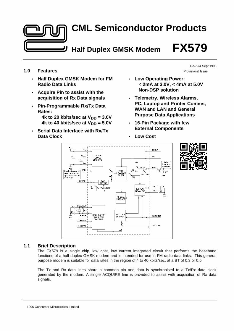
1.5.2 Description of Blocks and Signal Path(Reference Block Diagram Figure 1).
Power Supply CircuitsThese circuits produce the necessary internal voltage levels. Note that VDD and VBIAS should bedecoupled to VSS as shown.
Clock Oscillator and DividerThe transmit and (nominal) receive data rates are determined by division of the frequency present atthe XTALN pin, which may be generated by the on-chip Xtal oscillator or come from an externalsource. Any Xtal/Clock frequency in the range 1.0MHz to 5.0MHz (VDD = 3.0V) or 1.0MHz to 6.5MHz(VDD = 5.0V) may be used depending upon the desired data rate.
A division ratio to facilitate data rate setting is controlled by the logic level inputs on the CLKDIVA andCLKDIVB pins and is shown in Table 1 together with examples of how various 'standard' data ratesmay be derived from common Xtal frequencies.
Data Rate = Xtal or Clock Frequency
Division Ratio
Division ratio = Xtal Clock FrequencyCLKDIVA CLKDIVB Xtal frequency
Table 1 Clock and Data Rates (in MHz and bits/sec, respectively)
Half Duplex GMSK Modem FX579
1996 Consumer Microcircuits Limited 8 D/579/4
Note: (1) Device operation is not guaranteed for operation above 40kbits/sec or below4kbits/sec.
(2) If a suitable Xtal or clock signal is not supplied, device supply current mayincrease.
Transmit Signal PathThe binary data applied to the DATAIO input is retimed within the chip on each rising edge of the Txclock and then converted into a 1V pk-pk binary signal centred around VBIAS. This signal is thenconnected to the input of the low pass Tx filter, and the output connected to the TXOP pin.
The Tx filter has a low pass frequency response, which is approximately Gaussian in shape, as shownin Figure 4. This minimises amplitude and phase distortion of the binary signal while providing sufficientattenuation of the high frequency components, which would otherwise cause interference into adjacentradio channels.
The actual filter bandwidth to be used in any particular application will be determined by the overallsystem requirements. The attenuation versus frequency response of the transmit filtering provided bythis chip has been designed to meet the specifications for most GMSK modem systems, having a -3dBbandwidth switchable between 0.3 and 0.5 times the data bit rate.
Note that an external RC network is required between the TXOP pin and the input to the frequencymodulator. This network, which can form part of any dc level shifting and gain adjustment circuitry,forms an important part of the transmit signal filtering, and the ground connection to the capacitorshould be positioned to give maximum attenuation of high frequency noise into the modulator. Thecomponent values should be chosen so that the product of the resistance (in Ohms) and thecapacitance (in Farads) is:
0.34 / bit rate for BT of 0.30.21 / bit rate for BT of 0.5
(bit rate in bits per second)Suitable values for common bit rates are given in Table 2
The TXOP signal is centred around VBIAS, going positive for logic "1" level inputs to the DATAIO inputand negative for logic "0" inputs. Note that when in receive mode the input of the internal bufferamplifier driving the TXOP pin is connected to VBIAS.
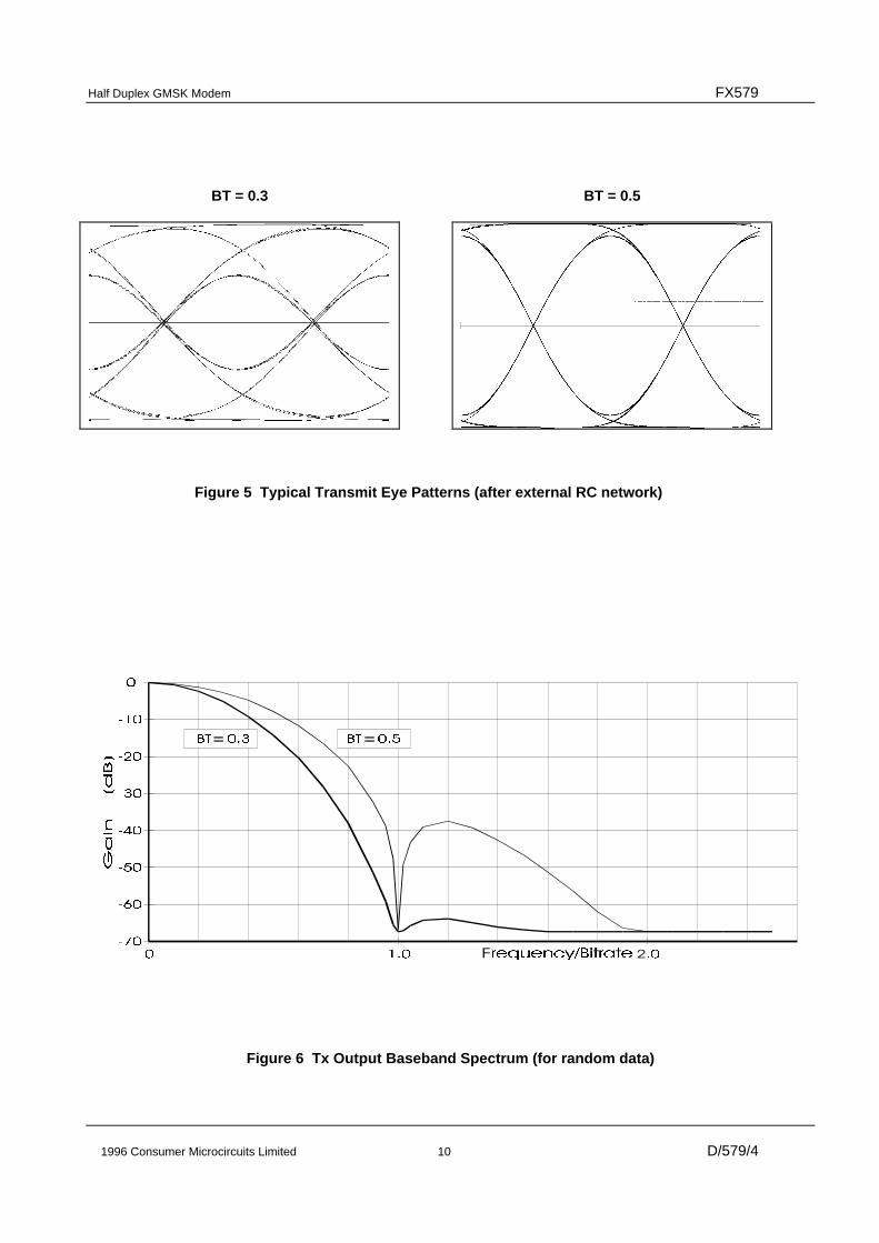
Figure 5 shows typical transmit eye patterns (measured after the external RC network) for BT values of0.3 and 0.5
Figure 6 shows the transmit output spectrum (measured after the external RC network) again for BTvalues of 0.3 and 0.5.
Half Duplex GMSK Modem FX579
1996 Consumer Microcircuits Limited 9 D/579/4
Figure 3 Typical Radio Application
Figure 4 Typical Attenuation v. Frequency Response of Tx Filter (after external RC network)
Figure 6 Tx Output Baseband Spectrum (for random data)
Half Duplex GMSK Modem FX579
1996 Consumer Microcircuits Limited 11 D/579/4
Receive Signal PathThe function of the Rx circuitry is to:
a) Accept an incoming signal from the radio's frequency discriminator at a defined level viasuitable external signal and dc level adjustment
b) Clean the signal by filteringc) Provide dc level thresholds for clock and data extractiond) Provide clock timing information for data extraction and external circuitse) Provide Rx data as an output in binary form
The output of the radio receiver's frequency discriminator after suitable external signal and leveladjustment is applied to the RXIN pin. With VDD = 5V, nominal input level when receiving a continuous"1111000011110000..." data pattern should be 1V pk-pk (level is proportional to VDD) centred around½ VDD. Positive going signal excursions about VBIAS at RXIN will produce a logic "1" on the DATAIOpin, negative going signal excursions will produce a logic "0".
The signal is then applied to the low pass Rx filter, which has a -3dB corner frequency of 0.56 times thedata bit rate, before being applied to the Level Measuring and Clock and Data Extraction blocks.
Level Measuring CircuitThe 'Level Measuring' block consists of two voltage detectors one of which measures the amplitude ofthe 'positive' peaks of the received signal, while the other measures the 'negative' peaks. Thesedetectors use the external capacitors connected to the DOC1 and DOC2 pins to form voltage hold orintegrator circuits.
Results of the two measurements are then processed within the modem to establish the optimum dclevel decision thresholds for the Clock and Data Extraction circuits, depending on the received signalamplitude, BT and any dc offset present.
The receive circuits operate in several control modes as defined by the logic level applied to theacquire pin. These are explained later - See 'Acquire Sequence'.
Rx Clock Extraction BlockThe 'Rx Clock Extraction' circuit is based on a zero crossing tracking loop which uses a multi resolutiondigital phase locked loop (PLL). The wide bandwidth mode allows for fast initial phase acquisition.Eight good zero crossings are required for correct operation.
The highest timing resolution is obtained when the PLL is in its narrow bandwidth mode. This mode ofoperation yields the least amount of phase jitter, which is responsible for the associated bit error rate(BER) performance degradation.
The PLL operating mode is defined by the logic level applied to the ACQUIRE pin - See 'AcquireSequence'.
Rx Data Extraction BlockThe 'Rx Data Extraction' circuit decides whether each received bit is a "1" or "0" by sampling thereceived signal, after filtering, in the middle of each bit period and comparing the sampled voltageagainst a threshold derived from the 'Level Measuring' circuit. This threshold is adapted from bit to bitto compensate for intersymbol interference depending on the chosen BT. The extracted data is outputfrom the DATAIO pin and should be sampled externally on the rising edge of the received data clock.
Half Duplex GMSK Modem FX579
1996 Consumer Microcircuits Limited 12 D/579/4
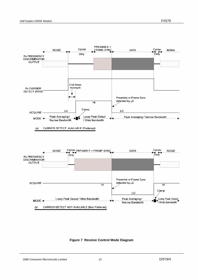
Acquire SequenceFigure 7 shows the typical received output from a radio's frequency discriminator. A data transmissionin general begins with a burst of unmodulated carrier followed by preamble of, for example "11001100--" and then frame sync, so as to allow the receive modem to establish timing and level lock as soon aspossible, before the message is sent.
In most applications there will also be a dc step in the output voltage from the receiver FM discriminatordue to carrier frequency offsets as channels are changed or when the distant transmitter is turned on.
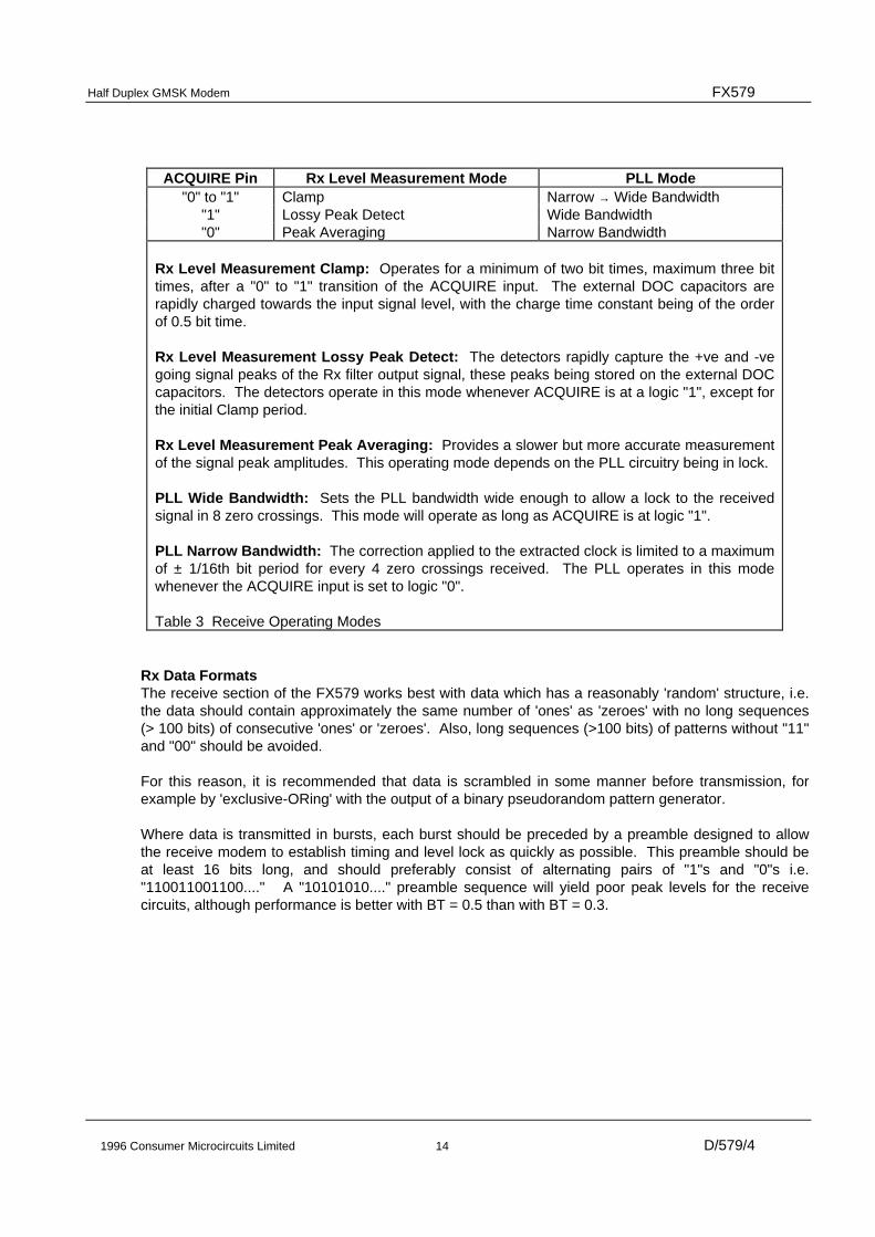
Figure 7 shows two possible receive operating modes of the FX579. The mode shown in (a) ispreferred and should be used when an external carrier detect signal is available, so as to provide thefastest possible acquisition of the received signal. The mode in (b) is suggested for when a carrierdetect signal is unavailable. The receive operating modes are determined by the logic state of theACQUIRE pin as explained in Table 3.
(a) Operation with a carrier detect (Preferred operating mode)
When an external carrier detect signal is available the µController should provide an ACQUIREpulse as shown. The ACQUIRE input is pulsed to a logic "1" a minimum of 2 bit times after thecarrier is detected (to allow for the receive filter delay) and just before preamble is expected (toreduce the probability of false frame sync detection under noisy conditions). The levelmeasurement DOC capacitors are then automatically clamped to the input signal for fastacquisition. The ACQUIRE input should remain at a logic "1" for a minimum of 16 bit times toenable the level measurement circuits to stabilise and the PLL to quickly achieve lock. TheACQUIRE input should then be taken to a logic "0" again, for better signal to noiseperformance, once the preamble or Frame Sync has been detected by the controllingmicroprocessor.
(b) Suggested operation without a carrier detect (Non-preferred operating mode)
When a carrier detect signal is not available, it is suggested that the modem be operated in theLossy Peak Detect/Wide Bandwidth mode (ACQUIRE pin at a logic "1") until the systemµController satisfactorily detects preamble and/or frame sync. Then the ACQUIRE pin shouldbe taken to a logic "0" for Peak Averaging/Narrow Bandwidth mode, so as to provide a bettersignal to noise performance for the rest of the message. The duration of initial unmodulatedcarrier plus preamble should be a minimum of 100 bit times to allow the voltages on theexternal DOC capacitors to stabilise. At the end of the message the ACQUIRE pin should bereturned to a logic "1".
The FX579 generally can tolerate dc offsets in the received signal of at least ±0.5V with respect toVBIAS (VDD = 5V). The voltages on the DOC1 and DOC2 pins reflect the average peak positive andnegative excursions of the (filtered) received signal, and could therefore be used to derive a measureof the data signal amplitude and carrier frequency offset. Note, however, that these pins are drivenfrom very high impedance circuits, so that the dc load presented by any external circuitry shouldexceed 10MΩ to VBIAS.
Rx Level Measurement Clamp: Operates for a minimum of two bit times, maximum three bittimes, after a "0" to "1" transition of the ACQUIRE input. The external DOC capacitors arerapidly charged towards the input signal level, with the charge time constant being of the orderof 0.5 bit time.
Rx Level Measurement Lossy Peak Detect: The detectors rapidly capture the +ve and -vegoing signal peaks of the Rx filter output signal, these peaks being stored on the external DOCcapacitors. The detectors operate in this mode whenever ACQUIRE is at a logic "1", except forthe initial Clamp period.
Rx Level Measurement Peak Averaging: Provides a slower but more accurate measurementof the signal peak amplitudes. This operating mode depends on the PLL circuitry being in lock.
PLL Wide Bandwidth: Sets the PLL bandwidth wide enough to allow a lock to the receivedsignal in 8 zero crossings. This mode will operate as long as ACQUIRE is at logic "1".
PLL Narrow Bandwidth: The correction applied to the extracted clock is limited to a maximumof ± 1/16th bit period for every 4 zero crossings received. The PLL operates in this modewhenever the ACQUIRE input is set to logic "0".
Table 3 Receive Operating Modes
Rx Data FormatsThe receive section of the FX579 works best with data which has a reasonably 'random' structure, i.e.the data should contain approximately the same number of 'ones' as 'zeroes' with no long sequences(> 100 bits) of consecutive 'ones' or 'zeroes'. Also, long sequences (>100 bits) of patterns without "11"and "00" should be avoided.
For this reason, it is recommended that data is scrambled in some manner before transmission, forexample by 'exclusive-ORing' with the output of a binary pseudorandom pattern generator.
Where data is transmitted in bursts, each burst should be preceded by a preamble designed to allowthe receive modem to establish timing and level lock as quickly as possible. This preamble should beat least 16 bits long, and should preferably consist of alternating pairs of "1"s and "0"s i.e."110011001100...." A "10101010...." preamble sequence will yield poor peak levels for the receivecircuits, although performance is better with BT = 0.5 than with BT = 0.3.
Half Duplex GMSK Modem FX579
1996 Consumer Microcircuits Limited 15 D/579/4
Figure 8 Tx/Rx Data and Clock Timings
Half Duplex GMSK Modem FX579
1996 Consumer Microcircuits Limited 16 D/579/4
Tx/Rx Switching(Refer to Figure 8)
Rx to Tx Transition - following a "0" to "1" transition on the TXRXN input:
a) If DATACLK is at a logic "1" it will go to a logic "0" (t1 max = 1µs), or if at logic "0" will stay low.It will then remain at "0" for a minimum of 2 bit times, maximum of 3 bit times, before the first+ve transmit clock edge occurs.
b) The DATAIO line will go to a high impedance state ready for Tx data to be applied (t2 max =1µs). Data on the DATAIO line should be set up and ready for when the first +ve transmit clockedge occurs. This edge will clock the first bit of data into the transmit filter. Succeeding -veclock edges may be used by the µController to ensure that data is always set up when +veedges occur.
c) TXOP is opened to the transmit path upon occurrence of the first +ve clock edge. Due to thedelay of the filter, the centre of Bit 1 will appear at the pin a maximum of 2 bit times (BT = 0.5)or 2.5 bit times (BT = 0.3) later.
d) At the end of a message the transmit output will remain in the state of the last bit sent.
e) If a long period of unmodulated carrier is required before a message (approximately 10ms ason MOBITEX), then the radio's transmitter should be keyed up with the FX579 modem still inRx mode.
Tx to Rx Transition - following a "1" to "0" transition on the TXRXN input:
a) DATACLK continues at the nominal bit rate in a free-running mode until locked to a receivesignal, e.g. after a satisfactory ACQUIRE sequence.
b) The buffer driving the TXOP pin is immediately connected to VBIAS.
c) The DATAIO line immediately goes low impedance and starts sending Rx data.
d) There is a 3-bit delay in the receive path before RXIN input data can appear at the DATAIOpin.
Half Duplex GMSK Modem FX579
1996 Consumer Microcircuits Limited 17 D/579/4
1.6 Application Notes
Radio Channel RequirementsTo achieve legal adjacent channel performance at high bit rates, a radio with an accurate carrierfrequency and an accurate modulation index is required.
For optimum channel utilization, (eg. low BER and high data rates) attention must be made to thephase and frequency response of both the IF and baseband circuitry, and to the accuracy of the Tx/Rxcarrier frequencies.
Bit Rate, BT and BandwidthThe maximum data rate that can be transmitted over a radio channel depends on the following:
Channel spacingAllowable adjacent channel interferenceTx filter bandwidthPeak carrier deviation (Modulation Index)Tx and Rx carrier frequency accuraciesModulator and demodulator linearityReceive IF filter frequency and phase characteristicsUse of error correction techniquesAcceptable error-rate
As an example, for MOBITEX operation, a raw data rate of 8kbits/sec at 12.5kHz channel spacing maybe achievable - depending on local regulatory requirements, using a ± 2kHz maximum deviation, a BTof 0.3, and no more than 1.5kHz discrepancy between Tx and Rx carrier frequencies.
Forward error correction (FEC) could then be used with interleaving to reduce the effect of burst errors.
Reducing the data rate to 4800bits/sec would allow the BT to be increased to 0.5, thus improving theerror rate performance.
For CDPD operation, a 19 200 bits/sec raw data rate at 30kHz channel spacing may be utilised with a± 8kHz maximum deviation, a BT of 0.5, and no more than 3kHz discrepancy between Tx and Rxcarrier frequencies.
These examples should be used for guidance purposes only. Regulatory compliance of a designshould be verified.
FM Modulator, Demodulator and IFFor optimum performance, the 'eye' pattern of the received signal (when receiving random data)applied to the FX579 should be as close as possible to the transmit 'eye' pattern examples shown inFigure 5.
Of particular importance are general symmetry, cleanliness of the zero crossings, lack of overshootand, for a BT of 0.3, the relative amplitude of the inner eye opening.
To achieve this, attention must be paid to:
a) Linearity and frequency/phase response of the Tx frequency modulator.(Unless the transmit data is especially encoded to remove low frequency components,the modulator frequency response should extend down to a few hertz. Hence twopoint modulation is necessary for synthesised radios.)
Half Duplex GMSK Modem FX579
1996 Consumer Microcircuits Limited 18 D/579/4
b) Bandwidth and phase response of the Rx IF filters.
c) Accuracy of the Tx and Rx carrier frequencies.(Any difference will shift the received signal towards one of the skirts of the IF filterresponse.)
AC Coupling of Tx and Rx SignalsIdeally, the transmit path to the modulator should be dc coupled. Similarly, the Rx demodulated signalafter external adjustment should be dc coupled to the FX579 RXIN pin, providing a signal symmetricallycentred about VBIAS. Figure 9 shows the bit error rate (BER) performance under these conditions forBT values of 0.3 and 0.5 in peak averaging mode. However, practical applications may require accoupling from the FX579's transmit output to the frequency modulator and between the receiver'sfrequency discriminator and the FX579's receive input. This creates two problems:
a) AC coupling of the signal will degrade the FX579's bit error rate (BER) performance, as shownin Figure 10 for a data rate of 8kbits/sec, with VDD = 5V and BT = 0.3.
b) AC coupling at the receive input will transform a step in the voltage at the discriminator outputto a slowly decaying pulse which can confuse the FX579's level measuring circuits. Sufficienttime should therefore be allowed for the signal into the FX579 to settle before the ACQUIREline is activated.
It is recommended that a data message does not contain long sequences of consecutive ones orzeroes and that the Tx and Rx path frequency responses have cut off frequencies of ≤5Hz and ≤20Hzrespectively, for a data rate of 8kbits/sec and BT = 0.3.
Two-Point ModulationWhen designing the FX579 into a radio that uses a frequency synthesiser, a two point modulationtechnique is recommended. This is to prevent the radio's PLL circuitry from counteracting themodulation process, and so provide a clean flat modulation response down to dc.
The transmit output (after the external RC) should be suitably buffered before being applied to theradio's synthesizer. The drive should be applied to both the Voltage Controlled Oscillator andReference Oscillator Modulation inputs with suitable ac/dc levels and with correct phase to achievegood cancellation of the loop's feedback and so provide a flat modulation response.
Half Duplex GMSK Modem FX579
1996 Consumer Microcircuits Limited 19 D/579/4
Figure 9 Typical Bit Error Rate Performance
Figure 10 Effect of AC Coupling on Typical Bit Error Rate (8000 bits/sec, BT = 0.3)
Half Duplex GMSK Modem FX579
1996 Consumer Microcircuits Limited 20 D/579/4
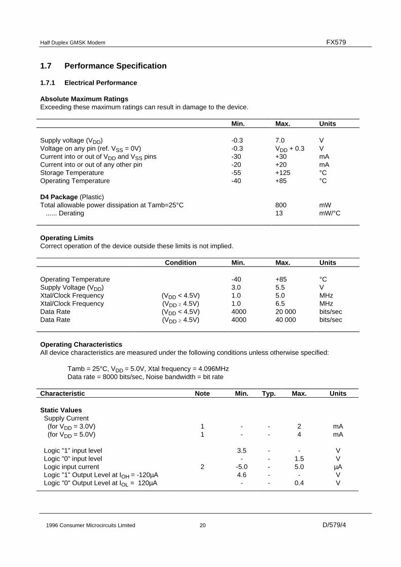
1.7 Performance Specification
1.7.1 Electrical Performance
Absolute Maximum RatingsExceeding these maximum ratings can result in damage to the device.
Min. Max. Units
Supply voltage (VDD) -0.3 7.0 VVoltage on any pin (ref. VSS = 0V) -0.3 VDD + 0.3 VCurrent into or out of VDD and VSS pins -30 +30 mACurrent into or out of any other pin -20 +20 mAStorage Temperature -55 +125 °COperating Temperature -40 +85 °C
D4 Package (Plastic)Total allowable power dissipation at Tamb=25°C 800 mW ...... Derating 13 mW/°C
Operating LimitsCorrect operation of the device outside these limits is not implied.
Condition Min. Max. Units
Operating Temperature -40 +85 °CSupply Voltage (VDD) 3.0 5.5 VXtal/Clock Frequency (VDD < 4.5V) 1.0 5.0 MHzXtal/Clock Frequency (VDD ≥ 4.5V) 1.0 6.5 MHzData Rate (VDD < 4.5V) 4000 20 000 bits/secData Rate (VDD ≥ 4.5V) 4000 40 000 bits/sec
Operating CharacteristicsAll device characteristics are measured under the following conditions unless otherwise specified:
Tamb = 25°C, VDD = 5.0V, Xtal frequency = 4.096MHzData rate = 8000 bits/sec, Noise bandwidth = bit rate
Characteristic Note Min. Typ. Max. Units
Static Values Supply Current (for VDD = 3.0V) 1 - - 2 mA (for VDD = 5.0V) 1 - - 4 mA
Logic "1" input level 3.5 - - V Logic "0" input level - - 1.5 V Logic input current 2 -5.0 - 5.0 µA Logic "1" Output Level at IOH = -120µA 4.6 - - V Logic "0" Output Level at IOL = 120µA - - 0.4 V
Half Duplex GMSK Modem FX579
1996 Consumer Microcircuits Limited 21 D/579/4
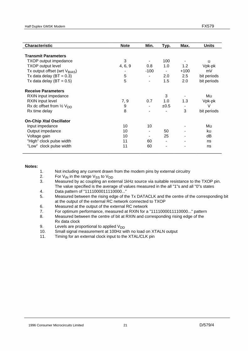
Characteristic Note Min. Typ. Max. Units
Transmit Parameters TXOP output impedance 3 - 100 - Ω TXOP output level 4, 6, 9 0.8 1.0 1.2 Vpk-pk Tx output offset (wrt VBIAS) - -100 - +100 mV Tx data delay (BT = 0.3) 5 - 2.0 2.5 bit periods Tx data delay (BT = 0.5) 5 - 1.5 2.0 bit periods
Receive Parameters RXIN input impedance 3 - MΩ RXIN input level 7, 9 0.7 1.0 1.3 Vpk-pk Rx dc offset from ½ VDD 9 - ±0.5 - V Rx time delay 8 - - 3 bit periods
Notes:1. Not including any current drawn from the modem pins by external circuitry2. For VIN in the range VSS to VDD3. Measured by ac coupling an external 1kHz source via suitable resistance to the TXOP pin.
The value specified is the average of values measured in the all "1"s and all "0"s states4. Data pattern of "1111000011110000..."5. Measured between the rising edge of the Tx DATACLK and the centre of the corresponding bit
at the output of the external RC network connected to TXOP6. Measured at the output of the external RC network7. For optimum performance, measured at RXIN for a "1111000011110000..." pattern8. Measured between the centre of bit at RXIN and corresponding rising edge of the
Rx data clock9. Levels are proportional to applied VDD10. Small signal measurement at 100Hz with no load on XTALN output11. Timing for an external clock input to the XTAL/CLK pin
Half Duplex GMSK Modem FX579
1996 Consumer Microcircuits Limited 22 D/579/4
1.7.2 Packaging
Figure 11 SOIC Mechanical Outline: Order as part no. FX579D4
Half Duplex GMSK Modem FX579
Handling precautions: This product includes input protection, however, precautions should be taken to preventdevice damage from electro-static discharge. CML does not assume any responsibility for the use of anycircuitry described. No IPR or circuit patent licences are implied. CML reserves the right at any time withoutnotice to change the said circuitry and this product specification. CML has a policy of testing every productshipped using calibrated test equipment to ensure compliance with this product specification. Specific testingof all circuit parameters is not necessarily performed.