33
ANALOG INTERFACE CARD - A2D2A For Texas Instruments DSP Development Systems Hardware for Signal Processing &Control

ANALOG INTERFACE CARD - A2D2A For Texas Instruments DSP Development Systems
Hardware for Signal Processing & Control

A F F O R D A B L E H A R D W A R E I M P L E M E N T A T I O N
Hardware for Signal Processing and Control
© Antal Soos aSoos Inc.
1100 8th Ave. SW • Suite 704 Calgary, AB. T2P 3T9
Canada Phone 403.228.2842

ii
Abstract Analog to Digital & Digital to Analog converter interface card – A2D2A
The design of an interface card with eight analog inputs and four analog outputs is described in this technical paper. The standards stipulated in Texas Instruments TMS320 Cross-Platform Daughtercard Specification, Revision 1.0, [1] have been followed in the design process. This card can be used with any Texas Instruments TI320 DSP development system, as presented in Figure 1. The A2D2A generates all of the necessary voltages on board from the 5V power, which is available according to the TMS320 Cross-Platform Daughtercard Specifications. For an easy interface, the common BNC coaxial connectors are used for the input and output connections. To reduce the manufacturing costs, the card is designed using a two layer PCB.
-10 V < input < + 10V
(-1 0 V ... +1 0 V)
-5 V < output < + 5V
8 input 4 output
D S K o r
E V M
A 2 D 2A
Figure 1 Usage of the A2D2A daughtercard

Table of Contents
Abstract ii
Introduction 1
A2D2A Card 1
Highlights 2
Main Characteristics of the A2D2A Card 3
Description 4
Timing Control 5
Timing Diagram 5
DSP and A2D2A Communication 6
Chip Select 4
Address Space 6
Control Signals 7
Input Buffer 8
Output Buffer 8
Reference voltages 9
Positive Reference 9
Negative Reference 9
Interpretation 10
Shielding 11
Power Source 11
Enhancement of A/D Conversion 15
Programming the PLD 17
References 18
A2D2A Attached Documents 19

T E C H N I C A L P A P E R
1
Introduction Signal processing and control algorithms have increased in complexity since their introduction in the 1960’s. The main research tools that have contributed to the development of these algorithms are simulation tools such as matlab from The MathWorks. Although these tools have become increasingly sophisticated, the evaluation of the proposed algorithms can only be performed through real-time experiments.
The implementation of signal processing and control algorithms in real-time experiments has become more feasible with the introduction of Digital Signal Processors (DSP). For implementation, it is required that these DSPs be constructed in the form of embedded systems. On the market, more than one system is available with the ability to perform either general or specific functions. These systems are frequently characterized by high price and a low lifespan, due to their fast evolution. Fortunately, all the DSP manufacturers sell their DSPs in the form of a development system, consisting of a minimal hardware and a development software bundle at an affordable price. Although the supplied hardware enables real-time algorithm development, the required connection to the analog world is seldom included. In order to overcome this problem, the DSP development boards are equipped with expansion connectors which allow the attachment of daughtercards. Only a few companies, such as Analog Devices, Motorola, and Texas Instruments, dominate the market of DSPs.
In the following, the A2D2A interface card is described, which can be used by Texas Instruments development systems. This document is written not only with the intention to describe the developed A2D2A analog interface card but also with the objective is to present adequate information that aids the design of similar interface cards.
A2D2A Card The top view of the A2D2A daughtercard is shown in Figure 2. The upper eight BNC connectors are the analog inputs while the lower four BNC connectors are the analog outputs. To prevent both mechanical and electrical damage to the card, the top surface does not contain electrical elements.

T E C H N I C A L P A P E R
2
Figure 2 A2D2A: Top View
The electrical components are mounted on the bottom panel, as presented in Figure 3. The power converter section, located to the left, is between the two connectors. On the photo, the A/D section is to the upper right and the D/A section is to the lower right.
Figure 3 A2D2A: Bottom View
Highlights The A2D2A interface card, which facilitates communication between a TMS320 DSP development system and the analog environment, contains eight analog to digital (A/D) converter channels and four digital to analog (D/A) converter channels. For easy interfacing, the card uses common BNC coaxial connectors. The characteristic components of the interface card are listed in Table 1, while its block diagram is presented in Figure 4.

T E C H N I C A L P A P E R
3
The A2D2A card offers eight channels of 14-bit A/D conversions and a sampling rate which can attain a frequency of 83kHz, as well as four channels of 16-bit D/A conversions, making it ideal for data acquisition in multidimensional signal processing, transient capture, and control systems.
Any sampling rate from 0 Hz to 83 kHz can be derived from the internal clock of the DSP. Due to the employed A/D converter, AD7865AS-1, from Analog Devices, all channels are sampled simultaneously with virtually zero phase delay. Both the inputs and the outputs are equipped with appropriate amplifiers, which increase the input resistance and ensure the adequate output signal power.
Main Characteristics of the A2D2A Card
Input: single-ended, ±10.0 V, full scale, 250 GΩ impedance
Output: ± 5.0 V, full scale, low output impedance, up to ± 250 mA, thermal protection
A/D and D/A conversions: 14-bit and 16-bit respectively
Sampling rate: provided by an internal DSP clock, varies from 0 Hz to 83 kHz
Power: 1.0 A at +5 V supplied by the DSP board
Power
Converters
A/D
D/A
8
4
DSK or EVM Connectros
Figure 4 A2D2A: Block Representation

T E C H N I C A L P A P E R
4
Table 1: Characteristic Components of the A2D2A Card
Description Part Number Quantity Manufacturer
A/D Converter AD7865AS-1 2 Analog Devices
D/A Converter DAC7644E-ND 1 Burr-Brown
Voltage Reference LT1461DHS8-2.5 2 Linear Technology
Operational Amplifier OPA2277UA 9 Burr-Brown
Buffer BUF634U 4 Burr-Brown
Switching Power Supply
LT1533CS 3 Linear Technology
3.3V to 5V Interface SN74LVC4245APWR 3 Texas Instruments
Control Logic EMP7032AE 1 Altera Corporation
In order to simplify the card’s usage, the A2D2A is equipped with its own voltage converters of -12, -5, 5, and 12 V. These voltage converters are necessary for the board’s functioning.
Description One of the design objectives was to minimize the required interaction between the A2D2A card and the DSP. This was accomplished by the following manner. The timing of the A/D conversion is directly connected to the DSP’s clock output. When the A/D conversion is complete, it generates an interrupt on the DSP. This is used to initiate a Direct Memory Access (DMA) transfer to read the converted data. At the end of the DMA transfer, a new interrupt is generated, which signals to the DSP that the A/D data is ready for processing. The D/A conversion control is further simplified when the write action automatically generates the D/A conversion. Next, the different units of the A2D2A card are described.
T E C H N I C A L P A P E R
5
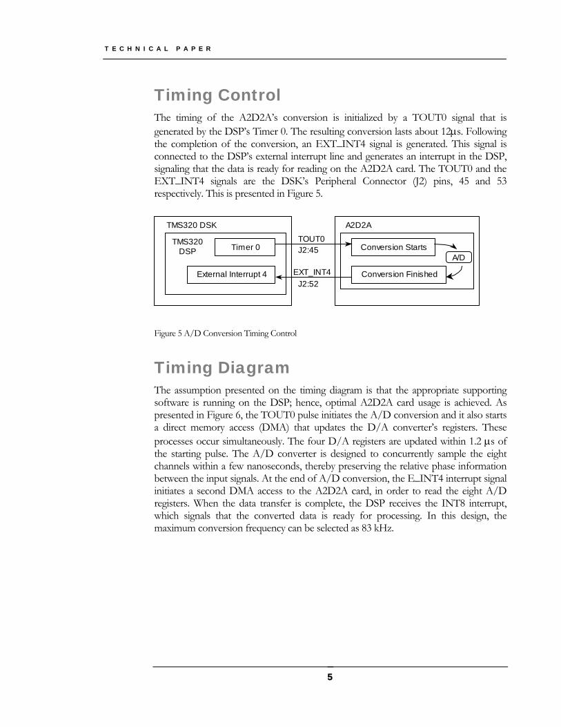
Timing Control The timing of the A2D2A’s conversion is initialized by a TOUT0 signal that is generated by the DSP’s Timer 0. The resulting conversion lasts about 12μs. Following the completion of the conversion, an EXT_INT4 signal is generated. This signal is connected to the DSP’s external interrupt line and generates an interrupt in the DSP, signaling that the data is ready for reading on the A2D2A card. The TOUT0 and the EXT_INT4 signals are the DSK’s Peripheral Connector (J2) pins, 45 and 53 respectively. This is presented in Figure 5.
Timer 0
External Interrupt 4
TOUT0
TMS320 DSK
TMS320 DSP
A2D2A
A/D Conversion Starts
Conversion Finished EXT_INT4 J2:52
J2:45
Figure 5 A/D Conversion Timing Control
Timing Diagram The assumption presented on the timing diagram is that the appropriate supporting software is running on the DSP; hence, optimal A2D2A card usage is achieved. As presented in Figure 6, the TOUT0 pulse initiates the A/D conversion and it also starts a direct memory access (DMA) that updates the D/A converter’s registers. These processes occur simultaneously. The four D/A registers are updated within 1.2 μs of the starting pulse. The A/D converter is designed to concurrently sample the eight channels within a few nanoseconds, thereby preserving the relative phase information between the input signals. At the end of A/D conversion, the E_INT4 interrupt signal initiates a second DMA access to the A2D2A card, in order to read the eight A/D registers. When the data transfer is complete, the DSP receives the INT8 interrupt, which signals that the converted data is ready for processing. In this design, the maximum conversion frequency can be selected as 83 kHz.

T E C H N I C A L P A P E R
6
Figure 6 Timing Diagram for A2D2A
DSP and A2D2A Communication A detailed connection diagram, presenting the used signals, is shown in Figure 7. All the necessary control functions of the A2D2A are implemented in a Programmable Logic Device (PLD). The communication between the TMS320 DSK and the A2D2A card is facilitated by both the Memory Connector (J1) and Peripheral Connector (J2).
Chip Select
The access to the A2D2A registers is enabled if the chip select line J1:78, DC_CSa# is at a low level [1]. This chip select line on the Memory Connector’s 78 pin is recognized by the DSP as either: CE2, CE1, DS# or XCE0# depending on which EVM or DSK is used [1]. Specifically, the chip select line for the TMS320C6711DSK corresponds to CS2, which is activated if the DSP selects a memory space of 0xA0000000 and above.
Address Space
The address space of the A2D2A is only 16 words long, as presented in Table 2. The address lines are connected to the J1:26:23 pins of the DSP’s Memory Connector.
Table 2: The Memory Space of the A2D2A Card
Address Space Device Access
0 - 3 Future Use -

T E C H N I C A L P A P E R
7
4 - 7 A/D Channels 1-4 Read
8 - 11 A/D Channels 5-8 Read
12 - 15 D/A Channels 1-4 Write
Specifically, the space for the TMS320C6711DSK is located at the addresses from 0xA0000000 to 0xA000003C, by the increment of 0x4. Thus, the A/D Channel 1 can be read on address 0xA0000010, Channel 2 on address 0xA0000014, and so on. The D/A Channel 1 can be written on address 0xA0000030, D/A Channel 2 on 0xA0000034, and so on.
Control Signals
The access to A2D2A card is controlled by signals ARE#, AWE# and AOE# on the J1:73, J1:74 and J1:75 pins, respectively. It is mandatory that the DSP’s memory access timing is configured to satisfy the requirements stipulated in [2]and [3].
Figure 7 Connection Diagram of A2D2A

T E C H N I C A L P A P E R
8
Input Buffer In order to increase the input resistance a high precision operation amplifier, OPA2277 from Burr-Brown Corporation [4], is implemented. The OPA2277 is free from phase inversion and overload problems. It is stable in the implemented unity gain and provides excellent dynamic behavior.
The inputs of the A2D2A card are protected by the built in 1 kΩ series input resistors and diode clamps of the OPA2277. The inputs can withstand ±30 V differential inputs without damage. The protection diodes will, of course, conduct current when the inputs are over-driven. This may disturb the slewing behavior of the unity-gain follower application, but it will not damage the card [4].
Figure 8 Input Signal Buffering
Output Buffer The output is constructed by using a combination of an operation amplifier [4] and a high-speed buffer, BUF634, from Burr-Brown Corporation [5]. In this circuit configuration, as presented in Figure 9, the work is divided so that the operation amplifier is responsible for precision while the buffer provides the necessary current. An important advantage of this combination is that the power dissipation is managed by the buffer. The operation amplifier is loaded only by the low input current of the buffer. The circuit parameters such as offset, drift, noise, and harmonic distortion depend almost entirely upon the operation amplifier used in the circuit [6]. The output from the D/A converter is ± 2.5 V (full scale). For the selected R1 = R2 = 10.0 kΩ, the gain of the buffer becomes G = 1+(R2/R1) = 2 and the buffer’s output is in the range of ± 5.0 V (full scale). The maximum gain, for the ± 2.5 V full scale input voltage with the ± 12 V power supply, is when G = 4. This can be obtained by selecting R2 = 30.0 kΩ from the standard 1% resistor group.

T E C H N I C A L P A P E R
9
Figure 9 Output Signal Buffering
Reference voltages Positive Reference
The A/D and D/A converters require reference voltages of + 2.500 V and -2.500 V. To attain the highest precision, the LT1461 from Linear Technology has been selected [7]. The LT1461 combines very high accuracy and low drift with low supply current requirements. The design of the + 2.500V reference on the A2D2A card follows the recommendations from [7], as presented in Figure 10.
Figure 10 Positive Reference
Negative Reference
In order to obtain a high accuracy negative reference, the LT1461 is used in a modified connection, Figure 11. Although LT1461 is used as very stable negative reference, it requires a positive voltage applied to the Vin to bias internal circuitry. The input positive voltage must be current limited with a resistor to keep the output PNP transistor from turning on and driving the grounded output, Vout. The -2.500 V reference design is presented in Figure 11.

T E C H N I C A L P A P E R
10
Figure 11 Negative Reference
Interpretation The connection between the real word of the input/output voltages and the corresponding representation of this in the DSP is available in Table 3 and Table 4.
Table 3: A/D Conversion Characteristics
Voltage on the Input Raw Count Read Float Representation
- 10 V 0x8000 -10.0
0 V 0x0000 0.0
+ 10 V 0x7FFF 10.0
Table 4: D/A Conversion Characteristics
Voltage on the Output Raw Count Float Representation
- 5 V 0x0000 -5.0
0 V 0x8000 0.0
+5 V 0xFFFF 5.0

T E C H N I C A L P A P E R
11
Shielding During the initial tests it was observed that the proximity of the DSP and the A/D converters resulted in a noisier measurement than it is normally expected. After some experimentation a shielding was designed between the DSP and the A2D2A card, as presented in Figure 1. The shield is made of a thin sheet of tin according to the specifications given in Figure 13. The shield considerably reduces the noise on the measured data.
A2D2A
DSP - DSK Shield
Figure 12 The Mounted Shield
Figure 13 Shield Specifications
Power Source The DSP connectors only provide 3.3V power for the digital signal drivers and 5V with maximum 1.0 A electric power for the daughtercard powering. The components on the A2D2A card require -12V, -5V, 5V and 12V. Using external power sources would be expensive and it could also introduce more possibility for error. The simplest and safest approach is to generate the required powers on board, using DC/DC

T E C H N I C A L P A P E R
12
converters. For this reason, three DC/DC switching power converters were added to the A2D2A card, to convert the 5V input power to -12V, 7V and 12V. Further, linear regulators are used to produce the -5V from -12V and 5V from 7V. The linear regulators ensure that the noise on the power is even less than that on the already low noise switching DC/DC converters.
The most important component of the DC/DC converter is an ultra low-noise switching regulator, the LT1533CS from Linear Technology [7]. This controller is considered as the least noisy switching power supply on the market. For the design the suggested schema from Linear Technology is used with one modification. Since the suggested transformers were not available in small quantities, these were replaced with transformers made from toroid cores from Magnetics1 and manual winding. For the transformers the ZR-41605-TC core is selected. The inductive filters are using the OW-40705-TC cores.
1 Magnetics Division of Spang & Company
φE
H
φI
ΑS
Figure 14 Dimension Definitions
ZR-41605-TC: φE=15.9mm, φI=8.89mm, H=4.7mm, AS=0.153cm2, AL= 1.260 mH/turns
OW-40705-TC: φE=7.6mm, φI=3.18 mm, H=4.7mm, AS=0.-98cm2, AL = 8.350 mH/turns
φE is the external diameter, φI is the internal diameter, H is the height of the ferrite toroid core and AL is the magnetic field generated by a single turn.
The required number of turns is determined by the Faraday’s law [12]:
Φ⋅
⋅⎟⎟⎠
⎞⎜⎜⎝
⎛⋅
⋅⋅−=
S
SWFin
P Af
VVN
8102
18.0)( Eq 1
where :
Vin = 5V is the input DC voltage

13
VF= 1V is the forward voltage drop of the rectifier
fSW= 90 kHz is the selected switching frequency of the push-pull converter
AS= 0.153 cm2 effective cross section area of the core
Φp= 1000G = 0.1T peak flux density.
The number of primary turns is inversely proportional to peak flux density, Φp. In order to minimize the required number of turns, Np, it would seem desirable to maximize Φp. Above 50 kHz, increasing core losses forces a decrease in peak flux density. At 100 to 200 kHz, the peak flux density may have to be limited to 1200 or possibly to 800 G, respectively, to achieve an acceptable low core temperature rise [12].
The calculated required primary turns are Np = 11.62 → 12.
The secondary turns number is calculated through the secondary to primary turns ratio Ns /Np equations [7]
( )sind
FoutpS VVT
VVNN−⋅⋅
+=
min2/ Eq 2
where Vout = 12V and Vout = 7V, for the desired output voltages of +/-12V and 7V respectively.
VF = 0.5 forward drop of the rectifier [7]
Td = 0.44 the maximum duty cycle of each driver. For the LT1333 it is 0.44 [7]
Vinmin = 4.5V the expected minimum input voltage
Vs = 0.5VF = 0.5 switch on voltage [7].
The resulting ratio of the secondary to primary turns is Ns /Np = 44 and Ns /Np = 27 for +/-12V and 7V respectively.
The detailed winding is presented in Figure 15. The connection of the transformer is presented in Figure 16.

14
Figure 15 Inductor / Transformer winding
Np
Np
Ns
Ns
5VLT1533
ZR-41605-TC Toroid Core
Figure 16 Transformer connection
The power supply section of the A2D2A is presented in picture Figure 17, where the three transformers with six inductor-filters can be clearly observed between the Peripheral and Memory connectors.
Figure 17 The Realized Power Section

15
Enhancement of A/D Conversion In the implemented scenario, the A/D and D/A converters are utilized to convert specifically at the frequency of 50.0 kHz, which corresponds to 20 μs TTOUT0 period. The DSP collects from all the eight channels sixteen samples of consecutive A/D conversion data and after calculating the average of the A/D conversions, it makes the data available every 0.32 ms to the rest of the processes. The data flow, for this implementation, is presented on Figure 18. The filter on the measured data is further analyzed in the following.
0
127 tra->x
ad_buffer
0
0
7
3
TOUT0 CONVST#
BUSY1 E_INT4
ad_buffer
EDMA READY
0
3 rec->x
HWI IN8
A/D Buffer
D/A Buffer DSP A2D2A
0
3 0
3
0
3 EDMA CH1
TIMER 0
EDMA CH4
Fix/Float
Filter A/D
A/D
D/A
Figure 18 Data flow between A2D2A and the DSP
In general, the data yn from the A/D conversion contains some error due to the effects of the conversion process and the necessary signal conditioning prior to it. Usually this error can be modeled by an additive random signal ξn, superposed on the measured signal 0
ny [8]
nnn yy ξ+= 0 Eq 3
The accuracy of the A/D conversion improves if the signal to noise ratio is increased in the measurement. This is attained if multiple A/D conversions are performed and an average is calculated

16
∑=
−⋅=N
inNn yy
01
1 . Eq 4
For this procedure to be legitimate, the changes in the measured signal must be negligible on the length of the N sampling interval. Thus, 00
10
Nnnn yyy −− ≅≅ K and
∑=
−⋅+=N
inNnn yy
11
10 ξ Eq 5
where 0ny is the average of the measured signal. The increase in the signal to noise
ratio by the averaging process depends on the distribution of this random signal nξ . In a technical environment, this signal is usually a normally distributed random signal (white Gaussian noise) with zero mean. In the worst case scenario, this signal can be a uniformly distributed random signal. It is important to stress that if the mean of the random signal nξ is other than zero, the averaging process will not improve the measurements; rather, it will emphasize the bias of the nonzero mean.
When the random signal ),0(~ 2σξ Nn is normally distributed with zero mean and variance 2σ , then the noise reduction in the A/D conversion data, obtained by averaging, is [9]
∑=
−=N
inn N 1
11 ξξ where ( )21,0~ σξ Nn N Eq 6
Even though the averaged signal is also normally distributed with a zero mean, there is a N
1 reduction in the noise variance, which corresponds to a N1 reduction of the
standard deviation of the random signal. Consequently, the calculated average of 16 converted samples will improve the measurement accuracy by reducing four times the Gaussian noise in the measured data. In this way, the measurement accuracy improves by an extra two least significant valid bits.
When the random signal ( )ωωξ ,~ −Un is uniformly distributed in the interval ωξω ≤≤− n , the corresponding variance is 3/22 ωσ = [10]. It is well known that
the distribution of the sum of N uniformly distributed random signals rapidly approaches normal distribution, as increases [11]. Accordingly,
∑=
−=N
inn N 1
11 ξξ where ( )( )21,0~ σξ ⋅NN Nn Eq 7
17
The variance of the sum is linearly increasing by the number of summing elements. This means that if the random signal ( )ωωξ ,~ −Un is uniformly distributed, the signal accuracy cannot be improved by the averaging process. Fortunately, very few technical systems have uniformly distributed contaminating signals.
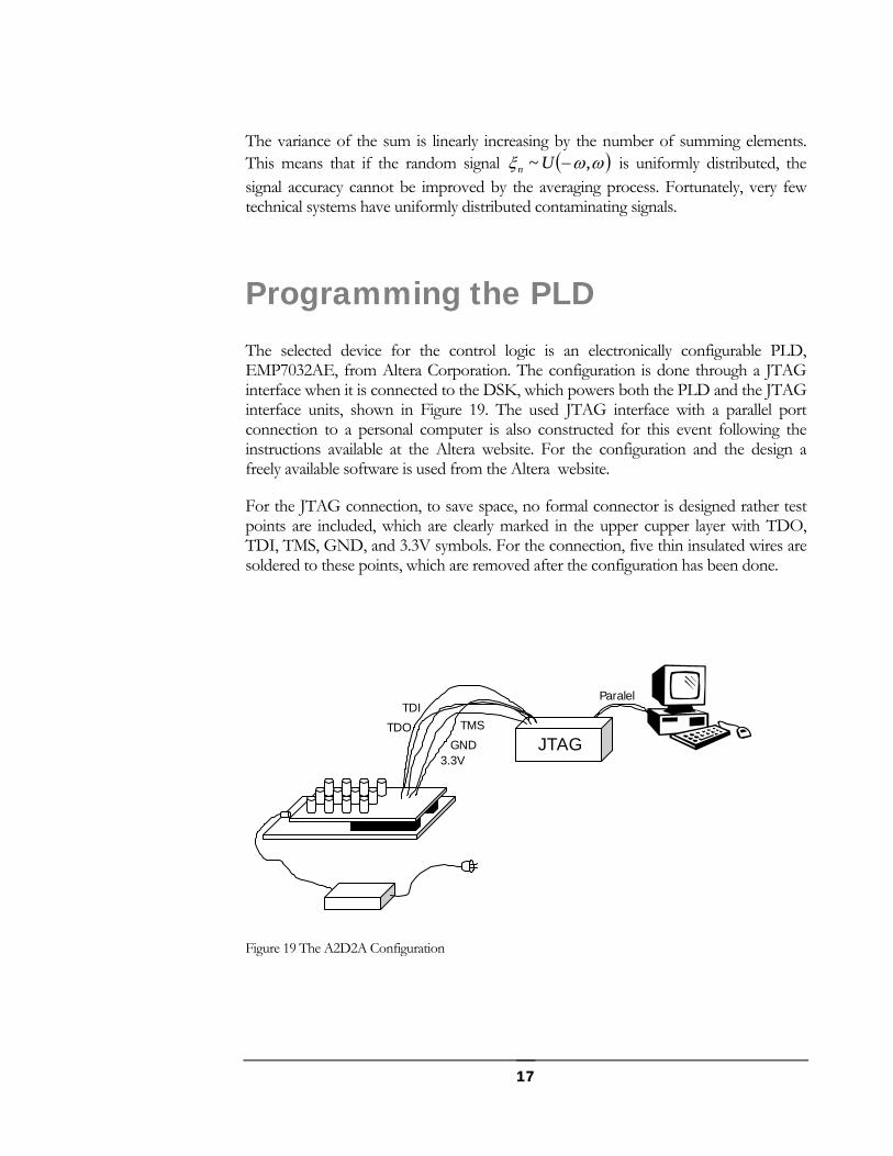
Programming the PLD The selected device for the control logic is an electronically configurable PLD, EMP7032AE, from Altera Corporation. The configuration is done through a JTAG interface when it is connected to the DSK, which powers both the PLD and the JTAG interface units, shown in Figure 19. The used JTAG interface with a parallel port connection to a personal computer is also constructed for this event following the instructions available at the Altera website. For the configuration and the design a freely available software is used from the Altera website.
For the JTAG connection, to save space, no formal connector is designed rather test points are included, which are clearly marked in the upper cupper layer with TDO, TDI, TMS, GND, and 3.3V symbols. For the connection, five thin insulated wires are soldered to these points, which are removed after the configuration has been done.
JTAG GND TMS
3.3V
TDI TDO
Paralel
Figure 19 The A2D2A Configuration

18
References [1] Bell, D., “TMS320 Cross-Platform Daughtercard Specification”, Texas
Instruments, Application Report, SPRA711, November, 2000.
[2] Datasheet, “AD7865 Four-Channel, Simultaneous Sampling, Fast, 14-Bit ADC”, Analog Devices Inc., Norwood, MA, USA, 2000.
[3] Datasheet, “DAC7644 16-Bit, Quad Voltage Output Digital-to-Analog Converter”, Burr-Brown Corporation, Tucson, AZ, USA, 1999.
[4] Datasheet, “High Precision Operational Amplifiers - OPA2277”, Burr-Brown Corporation, Tucson, AZ, USA, 1999.
[5] Datasheet, “250mA High-Speed Buffer - BUF634”, Burr-Brown Corporation, Tucson, AZ, USA, 1996.
[6] Vöhringer, U., “Combining an Amplifier with the BUF634”, Burr-Brown International GmbH, Application Bulletin AB-101, Tucson, AZ, USA, 2000.
[7] Datasheet, “Micropower Precision Low Dropout Series Voltage Reference Family - LT1461”, Linear Technology Corporation, Milpitas, CA, USA, 1999.
[8] Kay, S. M., “Fundamentals of Statistical Signal Processing, Volume 1: Estimation Theory”, Prentice Hall - Signal Processing Series, NJ, USA, 1993.
[9] Papoulis, A., and Pillai, S. U., “Probability, Random Variables, and Stochastic Processes”, Fourth Edition, McGraw-Hill, New York, NY, USA, 2002.
[10] Cramér, H., “Mathematical Methods of Statistics”, Princeton University Press, Princeton, NJ, USA, 1958.
[11] Mitra, S. K., “On the Probability Distribution of the Sum of Uniformly Distributed Random Variables”, SIAM Journal on Applied Mathematics, Vol. 20, No. 2, March, 1971, pp. 195-198.
[12] Pressman, I. A., “Switching Power Supply Design”, McGraw-Hill, New York, NY, USA, 1997.

19
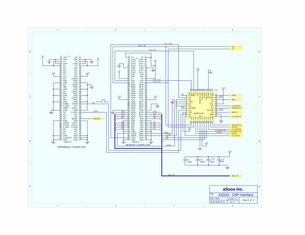
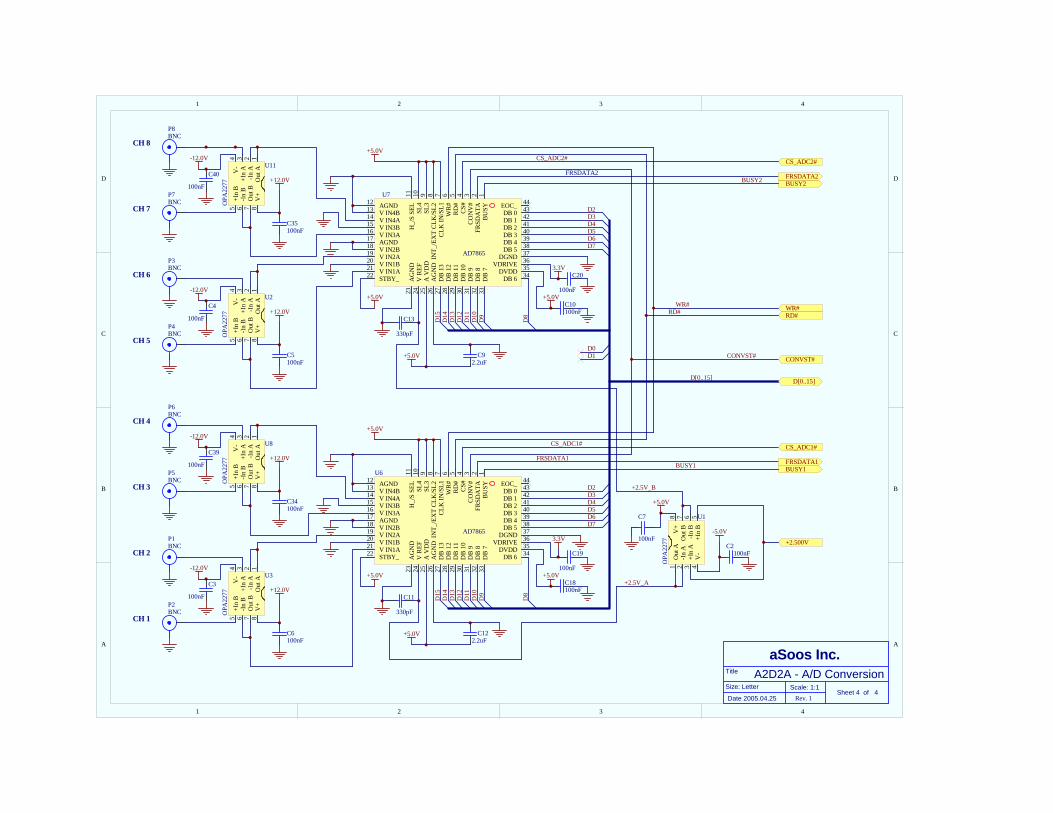
A2D2A Attached Documents
PLD Configuration Definition
Input/Output signal interpretation of the PLD
VHDL code of the PLD
A2D2A Schematics
Schematics Connection Block
Schematics 1/4
Schematics 2/4
Schematics 3/4
Schematics 4/4
PCB Image
Top PCB layer
Bottom PCB layer

Date: July 8, 2005 Top_LogyControl.bdf Project:
Page 1 of 1 Revision:
VCCA1 INPUT
VCCA2 INPUT
VCCA3 INPUT
VCCTIN INPUT
VCCFRSDATA1 INPUT
VCCBUSY1 INPUT
VCCFRSDATA2 INPUT
VCCBUSY2 INPUT
VCCCS INPUT
VCCARE INPUT
VCCAWE INPUT
VCCAOE INPUT
VCCA0 INPUT
INT4OUTPUT
WROUTPUT
RDOUTPUT
CONVSTOUTPUT
CS_ADC1OUTPUT
CS_ADC2OUTPUT
CS_DACOUTPUT
LOADDACSOUTPUT
RWOUTPUT
TROUTPUT
VCCD0BIDIR
VCCD1BIDIR
logyc
inst
A0 INPUTA1 INPUTA2 INPUTA3 INPUTTIN INPUTFRSDATA1 INPUTBUSY1 INPUTFRSDATA2 INPUTBUSY2 INPUTCS INPUTAOE INPUTARE INPUTAWE INPUTINT4 OUTPUTCONVST OUTPUTCS_ADC1 OUTPUTCS_DAC OUTPUTLOADDACSOUTPUTRD OUTPUTWR OUTPUTRW OUTPUTCS_ADC2 OUTPUTTR OUTPUTD0 BIDIRD1 BIDIR
I/O Type

Date: July 8, 2005 logyc.vhd Project:
Page 1 of 2 Revision:
-- Generated by Quartus II Version 2.2 (Build Build 147 12/02/2002)1-- Created on Wed Apr 02 02:42:20 20032
3LIBRARY ieee;4USE ieee.std_logic_1164.all;5
6-- Entity Declaration7
8ENTITY logyc IS9
-- {{ALTERA_IO_BEGIN}} DO NOT REMOVE THIS LINE!10PORT11(12
A0 : IN STD_LOGIC;13A1 : IN STD_LOGIC;14A2 : IN STD_LOGIC;15A3 : IN STD_LOGIC;16TIN : IN STD_LOGIC;17FRSDATA1 : IN STD_LOGIC;18BUSY1 : IN STD_LOGIC;19FRSDATA2 : IN STD_LOGIC;20BUSY2 : IN STD_LOGIC;21CS : IN STD_LOGIC;22AOE : IN STD_LOGIC;23ARE : IN STD_LOGIC;24AWE : IN STD_LOGIC;25INT4 : OUT STD_LOGIC;26CONVST : OUT STD_LOGIC;27CS_ADC1 : OUT STD_LOGIC;28CS_DAC : OUT STD_LOGIC;29LOADDACS : OUT STD_LOGIC;30RD : OUT STD_LOGIC;31WR : OUT STD_LOGIC;32RW : OUT STD_LOGIC;33CS_ADC2 : OUT STD_LOGIC;34TR : OUT STD_LOGIC;35D0 : INOUT STD_LOGIC;36D1 : INOUT STD_LOGIC37
);38-- {{ALTERA_IO_END}} DO NOT REMOVE THIS LINE!39
40END logyc;41
42-- Architecture Body43
44ARCHITECTURE logyc_architecture OF logyc IS45
46BEGIN47
48INT4 <= not ( BUSY1 or BUSY2);49CONVST <= TIN ;50CS_ADC1 <= CS or A3 or not A2 ;51CS_ADC2 <= CS or not A3 or A2 ;52CS_DAC <= CS or not A3 or not A2 or (ARE and AWE);53TR <= AOE;54LOADDACS <= CS or not A3 or not A2;55RW <= not AOE; 56WR <= AWE;57

Date: July 8, 2005 logyc.vhd Project:
Page 2 of 2 Revision:
RD <= ARE;5859
D0 <= FRSDATA1 when (CS or A3 or not A2 or AOE) = '0' else 60FRSDATA2 when (CS or not A3 or A2 or AOE) = '0' else 61'Z';62
D1 <= A1 when (CS or A3 or not A2 or AOE) = '0' else 63 A1 when (CS or not A3 or A2 or AOE) = '0' else 64
'Z';6566
END logyc_architecture;6768

1 2 3 4
A
B
C
D
4321
D
C
B
A
+2.500V-2.500V
POWPOW.Sch
D[0..15]+2.500V-2.500VCS_DAC#A0A1LOADDACS#RESET#R/W#
DACDAC.Sch
A0A1
CS_ADC1#CS_ADC2#
WR#RD#
CONVST#
BUSY2 RESET#
D[0..15]
CS_DAC#
LOADDACS#
R/W#
FRSDATA2FRSDATA1
BUSY1
DSPDSP.Sch
D[0..15]CONVST#CS_ADC2#CS_ADC1#
BUSY1
+2.500VWR#RD#
FRSDATA2FRSDATA1
BUSY2
ADCADC.Sch
5 V => -12 V, -5V, 5 V, 12 V
3.3 V
3.3 V, 5 v, 12 V-12 V, -5V
3.3 V, 5 v, 12 V-12 V, -5V
4 x (- 5V ... +5V)
8 x (-10 ... +10V)
BNC
BNC
TMS320 DaughtercardMemory & Peripheral Connector
aSoos Inc.A2D2A Block Diagram
Rev. 1Date 2005.04.25
Title
Sheet 0 of 4Size: Letter Scale: 1:1
5 V
1 2 3 4
A
B
C
D
4321
D
C
B
A
NC
1C
OL_
A2
DU
TY3
SYN
C4
Ct
5R
t6
FB7
NFB
8G
ND
9
Vc
10
#SH
DN
11
Rcs
l12
Rvs
l13
Vin
14
CO
L_B
15
PGN
D16
U21
LT15
33C
S
5V
+
C87
22uF
C79
100nF
R3115k
R3015k
R21
16.90k
C63
330pF
D9
10MQ040 D8
10MQ040 +
C83
22uF +
C60
22uF
-12.0V
R202.49k
R189.30k
NC
1C
OL_
A2
DU
TY3
SYN
C4
Ct
5R
t6
FB7
NFB
8G
ND
9
Vc
10
#SH
DN
11
Rcs
l12
Rvs
l13
Vin
14
CO
L_B
15
PGN
D16
U5
LT15
33C
S
5V
+ C2622uF
R615k
R715k
R4
16.09k
C17
330pF
D4
10MQ040 D210MQ040
+ C24
22uF
+ C23
22uF
+12.0V
R32.49k
R221.50k
NC
1C
OL_
A2
DU
TY3
SYN
C4
Ct
5R
t6
FB7
NFB
8G
ND
9
Vc
10
#SH
DN
11
Rcs
l12
Rvs
l13
Vin
14
CO
L_B
15
PGN
D16
U12
LT15
33C
S
5V
+
C57
22uF
C49
100nF
R1715k
R1515k
R14
16.90k
C33
330pF
D7
10MQ040 D610MQ040
+ C5522uF
+ C48
22uF
R132.49k
R1211.50k
GND1
IN2
BYP3 #SHDN 4
OUT 5U23
LT1964ES5-5
OUT 1SENSE 2BYP 3GND 4#SHDN5
NC6
NC7
IN8
U15
LT1962EMS8-5
-5.0V
C6610nF
+
C82100uF
C62
100nF
+ C44100uF
C3110nF
+5.0V7.023 V
12.043V
-12.069V
C64
330pF
C32
330pF
C16
330pF
195 kHz
195 kHz
195 kHz
Rv=Rg * [ (|V| - 2.5) / (2.5 + Rg*25uA) ]
Rv = Rg * [ ( V/1.25) - 1]
Rv = Rg * [ ( V/1.25) - 1]
C22
100nF
C84100nF
C56
100nF
C21
22nF
R91.50k
C27
220nF
C80
22nF
R291.50k
C85
220nF
C45
22nF
R161.50k
C50
220nF
C25
100nF
C41
100nF
-12.0V -5.0V +5.0V +12.0V
R83.48k
R321.13k
R331.13k
R53.48k
5V
R11.13k
If = 3 mA
-12.0V
D3LED
D11LED
D10LED
D5LED
D1LED
+5.0V
C42
2.2uF
C292.2uF
-5.0V
+2.500V
-2.500V
NC1
Vin2
SHDN3
GND4 NC 5Vout 6NC 7NC 8U10
LT1461-2.5
NC1
Vin2
SHDN3
GND4 NC 5Vout 6NC 7NC 8U9
LT1461-2.5
+5.0VR111.30k
R107.50k
C43
2.2uF
C28
2.2uF
1
4
5
6
8
273
T3
T
1
4
5
6
8
273
T2
T
1
4
5
6
8
273
T1
T
L8
100uH
L7
100uH
L5
100uH
L4
100uH
L3
100uH
L1
100uH
L225nH
L925nH
L625nH
+2.500V
-2.500V
aSoos Inc.A2D2A - Power suply
Rev. 1Date 2005.04.25
Title
Sheet 1 of 4Size: Letter Scale: 1:1
1 2 3 4
A
B
C
D
4321
D
C
B
A
DB151
DB142
DB133
DB124
DB115
DB106
DB97
DB88
DB79
DB610
DB511
DB412
DB313
DB214
DB115
DB016
RSTSEL17
RST18
LOADDACS19
R/W#20
A121
A022
CS_23
DGND24
NC 48
V OUTA 43
V REFL AB Sense 42
V REFL AB 41
V REFH AB 40
V REFH AB Sense 39
V OUTB Sense 38
V OUTB 37
V OUTC Sense 36
V OUTC 35
V REFH CD Sense 34
NC 47
NC 46
NC 45
V OUTA Sense 44
V REFH CD 33
V REFL CD 32
V DD 25V CC 26AGND 27V SS 28V outD 29
V REFL CD Sense 31
V OUTD Sense 30
U19
DAC7644
P9BNC
P10BNC
P11BNC
P12BNC
CH 1
CH 2
CH 3
CH 4
BW1
NC2
VIN3
V-4 NC 5Vo 6V+ 7NC 8U17
BUF634U
BW1
NC2
VIN3
V-4 NC 5Vo 6V+ 7NC 8U26
BUF634U
Out
A1
-In
A2
+In
A3
V-
4+I
n B
5
-In
B6
Out
B7
V+
8
U18
OPA
2277
R1910k0
R2510k0
+12.0V
C672.2uF
C722.2uF +
C47
22uF
+C46
22uF
C51
2.2uF
-12.0V
+12.0V
C712.2uF
C90
2.2uF
-12.0V
-12.0V
R23
10k0
+12.0VC58
2.2uF
R2410k0
BW1
NC2
VIN3
V-4 NC 5Vo 6V+ 7NC 8U24
BUF634U
BW1
NC2
VIN3
V-4 NC 5Vo 6V+ 7NC 8U27
BUF634U
Out
A1
-In
A2
+In
A3
V-
4+I
n B
5
-In
B6
Out
B7
V+
8
U20
OPA
2277
R2210k0
R2710k0
+12.0V
C882.2uF
C682.2uF +
C65
22uF
+C74
22uF
C73
2.2uF
-12.0V
+12.0V
C862.2uF
C89
2.2uF-12.0V
-12.0V
R2610k0
+12.0VC61
2.2uF
R28
10k0
C752.2uF
C762.2uF
+ C93100uF
+
C94100uF
-5.0V
+5.0V
VccA1
T/R#2
A03
A14
A25
A36
A47
A58
A69
A710
GND11
GND12 GND 13B7 14B6 15B5 16B4 17B3 18B2 19B1 20B0 21OE# 22NC 23VccB 24U14
74LVXC3245
VccA1
T/R#2
A03
A14
A25
A36
A47
A58
A69
A710
GND11
GND12 GND 13B7 14B6 15B5 16B4 17B3 18B2 19B1 20B0 21OE# 22NC 23VccB 24U16
74LVXC3245
VccA1
T/R#2
A03
A14
A25
A36
A47
A58
A69
A710
GND11
GND12 GND 13B7 14B6 15B5 16B4 17B3 18B2 19B1 20B0 21OE# 22NC 23VccB 24U22
74LVXC3245
+5.0V
+5.0V
+5.0VC38
100nF
C54100nF
C37
100nF
C53
100n
F
C70
100nF
C69
100nF
3.3V
3.3V
3.3V
D0D1D2D3D4D5D6D7
D8D9D10D11D12D13D14D15
D[0..15]
-5V...+5V
-5V...+5V
-5V...+5V
-5V...+5V
Out
A1
-In
A2
+In
A3
V-
4+I
n B
5-I
n B
6O
ut B
7V
+8
U13OPA2277
Out
A1
-In
A2
+In
A3
V-
4+I
n B
5-I
n B
6O
ut B
7V
+8
U25
OPA
2277
-2.500V
+2.500V+5.0V
-5.0V
C36
100nF
C30100nF
C91
100nF
-2.500V
-5.0VC92
100nF
+5.0V
+2.5
00V
+2.500V
-2.500V
C52330pF
C59
330pF
C78330pF
C81
330pF
CS_DAC#A0A1
LOADDACS#RESET#
-2.500V
+2.500V
3.3V / 5V
3.3V / 5V
R/W# R/W#
A0A1
CS_DAC#
LOADDACS#RESET#
D[0
..15]
C77 100nF
aSoos Inc.A2D2A - D/A Conversion
Rev. 1Date 2005.04.25
Title
Sheet 2 of 4Size: Letter Scale: 1:1
1 2 3 4
A
B
C
D
4321
D
C
B
A
5V 15V2
EA21 3EA204
EA19 5EA186
EA17 7EA168
EA15 9EA1410
GND 11GND12
EA13 13EA1214
EA11 15EA1016
EA9 17EA818
EA7 19EA620
5V 215V22
EA5 23EA424
EA3 25EA226
BE3# 27BE2#28
BE1# 29BE0#30
GND 31GND32
ED31 33ED3034
ED29 35ED2836
ED27 37ED2638
ED25 39ED2440
3.3V 413.3V42
ED23 43ED2244
ED21 45ED2046
ED19 47ED1848
ED17 49ED1650
GND 51GND52
ED15 53ED1454
ED13 55ED1256
ED11 57ED1058
ED9 59ED860
GND 61GND62
ED7 63ED664
ED5 65ED466
ED3 67ED268
ED1 69ED070
GND 71GND72
ARE# 73AWE#74
AOE# 75ARDY76
CE3# 77CE2#78
GND 79GND80
J1
DSK6711
12V 1-12V2
GND 3GND4
5V 55V6
GND 7GND8
5V 95V10
N/C 11N/C12
N/C 13N/C14
N/C 15N/C16
N/C 17N/C18
3.3V 193.3V20
CLKX0 21N/C22
FSX0 23DX024
GND 25GND26
CLKR0 27N/C28
FSR0 29DR030
GND 31GND32
CLKX1 33N/C34
FSK1 35DX136
GND 37GND38
CLKR1 39N/C40
FSR1 41DR142
GND 43GND44
TOUT0 45TINPO46
N/C 47E_INT548
TOUT1 49TINP150
GND 51GND52
E_INT4 53N/C54
N/C 55N/C56
N/C 57N/C58
RESET 59N/C60
GND 61GND62
CNTL1 63CNTL064
STAT1 65STAT066
E_INT6 67E_INT768
N/C 69N/C70
N/C 71N/C72
N/C 73N/C74
GND 75GND76
GND 77ECLKOUT78
GND 79GND80
J2
DSK6711
A0A1
CS_ADC1#
CS_ADC2#
WR#
3.3V
C1100nF
CONVST#
3.3V
CS2->CS#
EA4->A2
EA5->A3
3.3V
3.3V3.3V
5V5V
3.3V
D0 D1D2 D3D4 D5D6 D7
D8 D9D10 D11D12 D13D14 D15
5V
BUSY2
RESET#
D[0..15]
5V
3.3V
C15100nF
CS_DAC#
LOADDACS#R/W#
C8100nF
3.3V
3.3V
C14100nF
BUSY1
RD#
LOADDACS#R/W#
TIN
INT4
D[0..15]
I/O/TDI1
I/O2
I/O3
GND4
I/O5
I/O6
I/O/TMS7
I/O8
VCC9
I/O10
I/O11
I/O12
I/O13
I/O14
I/O15
GN
D16
VC
C17
I/O18
I/O19
I/O20
I/O21
I/O22
I/O 23GND 24I/O 25I/O/TCK 26I/O 27I/O 28VCC 29I/O 30I/O 31I/O/TDO 32I/O 33I/O34
I/O35
GN
D36
I/GC
LK1
37I/O
E1n
38I/G
CLR
n39
I/OE2
/GC
LK2
40V
CC
41I/O
42I/O
43I/O
44 U4
EPM7032AE
FRSDATA1
FRSDATA2
D0D1
ARE#AOE#
AWE#
TDITDO
TMSTCK
EA3->A1
EA2->A0
PERIPHERAL CONNECTORMEMORY CONNECTOR
aSoos Inc.A2D2A - DSP Interface
Rev. 1Date 2005.04.25
Title
Sheet 3 of 4Size: Letter Scale: 1:1
1 2 3 4
A
B
C
D
4321
D
C
B
A
CLK
IN/S
L17
INT_
/EX
T C
LK/S
L28
SL3
9SL
410
H_/
S SE
L11
DB
733
DB
832
DB
931
DB
10
30D
B 1
129
DB
12
28D
B 1
327
AG
ND
26A
VD
D25
V R
EF24
AG
ND
23
EOC_ 44
DB 0 43
DB 1 42
DB 2 41
DB 3 40
DB 4 39
DB 5 38
DGND 37
VDRIVE 36
DVDD 35
DB 6 34
AGND12
V IN4B13
V IN4A14
V IN3B15
V IN3A16
AGND17
V IN2B18
V IN2A19
V IN1B20
V IN1A21
STBY_22
WR
#6
RD
#5
CS#
4
CO
NV
#3
FRSD
ATA
2
BU
SY1U6
AD7865
CLK
IN/S
L17
INT_
/EX
T C
LK/S
L28
SL3
9SL
410
H_/
S SE
L11
DB
733
DB
832
DB
931
DB
10
30D
B 1
129
DB
12
28D
B 1
327
AG
ND
26A
VD
D25
V R
EF24
AG
ND
23
EOC_ 44
DB 0 43
DB 1 42
DB 2 41
DB 3 40
DB 4 39
DB 5 38
DGND 37
VDRIVE 36
DVDD 35
DB 6 34
AGND12
V IN4B13
V IN4A14
V IN3B15
V IN3A16
AGND17
V IN2B18
V IN2A19
V IN1B20
V IN1A21
STBY_22
WR
#6
RD
#5
CS#
4
CO
NV
#3
FRSD
ATA
2
BU
SY1U7
AD7865
+12.0V
-12.0V
C35100nF
C40
100nF
P8BNC
P7BNC
P3BNC
P4BNC
P6BNC
P5BNC
P1BNC
P2BNC
CH 1
CH 2
CH 3
CH 4
CH 5
CH 6
CH 7
CH 8
C13
330pF
C11
330pF
+5.0V
+5.0V
+5.0V
+5.0V
+5.0V
+5.0V
3.3V
3.3V
C20
100nF
C10100nF
C19
100nF
C18100nF
D2D3D4D5D6D7
D2D3D4D5D6D7
D8
D9
D10
D11
D12
D13
D14
D15
D8
D9
D10
D11
D12
D13
D14
D15
D[0..15]
CONVST# CONVST#
WR#RD#
CS_ADC2#
CS_ADC1#
CS_ADC2#
CS_ADC1#
Out
A1
-In
A2
+In
A3
V-
4+I
n B
5
-In
B6
Out
B7
V+
8
U11
OPA
2277
BUSY1
+12.0V
-12.0V
C5100nF
C4
100nF
Out
A1
-In
A2
+In
A3
V-
4+I
n B
5
-In
B6
Out
B7
V+
8
U2
OPA
2277
+12.0V
-12.0V
C34100nF
C39
100nF
Out
A1
-In
A2
+In
A3
V-
4+I
n B
5
-In
B6
Out
B7
V+
8
U8
OPA
2277
+12.0V
-12.0V
C6100nF
C3
100nF
Out
A1
-In
A2
+In
A3
V-
4+I
n B
5
-In
B6
Out
B7
V+
8
U3
OPA
2277
Out
A1
-In
A2
+In
A3
V-
4+I
n B
5-I
n B
6O
ut B
7V
+8 U1
OPA
2277 +2.500V
+5.0V
-5.0V
C92.2uF
C7
100nFC2
100nF
WR#RD#
+5.0V
+5.0V C122.2uF
BUSY2
FRSDATA1
+2.5V_A
+2.5V_B
BUSY2
BUSY1
D[0..15]
FRSDATA1
FRSDATA2
D0D1
FRSDATA2
aSoos Inc.A2D2A - A/D Conversion
Rev. 1Date 2005.04.25
Title
Sheet 4 of 4Size: Letter Scale: 1:1


