DescriptionEMC immunity, especially immunity against inverterswitching noise, is important for positioning encoderfeedback systems of industrial drives. This designdemonstrates a high EMC immunity RS485 transceiversolution which can be used on both the drive andencoder, such as Tamagawa™, EnDat 2.2, BiSS®,and so forth. The design supports a wide input voltageof 5 V. A connector with 3.3-V logic I/O signals and a3.3-V power supply allows direct interface with thehost processor to run the master protocol and powerthe processor. To meet the supply range of theselected encoder, the design offers an output voltageto the encoder equal to the Vin. This design’s powersupply offers protection against overvoltage and shortcircuit, according to the selected encoder’s voltagerange, to prevent damage during a cable short. Thedesign has been tested for up to a 50-m cable lengthwith the Tamagawa encoder.
Features• 5-V half-duplex RS485 transceiver with up to 50-
Mbps baud rate and improved EMC immunityagainst IEC61000-4-4
• Hardware supports 2-wire interfaces standards,such as Tamagawa, or 4-wire RS485 interfacestandards, such as EnDat2.2 and BiSS
• 5-V supply half-duplex RS485 transceiverTHVD1550 with 16-kV IEC-ESD and 4-kV EFTeliminates cost for external ESD components.
• Highest immunity against IEC61000-4-4 fastelectrical transients versus other industry standardRS485 transceivers, validated in system tests
• Designed to meet IEC61800-3 EMC immunity forvariable-speed drives without the need foradditional protection devices, such as TVS diodes,when used in applications with encoders usingshielded cables
• The design is in BoosterPack™ plug-in moduleform factor, with a connector compatible to the TILaunchPad™ Development Kit for easy evaluationof Tamagawa with a C2000™ MCU
Applications• Servo CNC and Robotics• AC Inverter and VF Drives• Position Sensor (Encoders)• Industrial Robots
High EMC Immunity RS485 Interface Reference Design for TamagawaEncoders
An IMPORTANT NOTICE at the end of this TI reference design addresses authorized use, intellectual property matters and otherimportant disclaimers and information.
1 System DescriptionAbsolute digital encoders acquire absolute position or rotary angle and feedback, typically in industrialdrives, such as servo drives, CNC, and robotics EE.
Multiple protocol standards are based on RS485/RS422, with synchronous or asynchronouscommunication and a protocol-specific encoder supply voltage range. Drive customers are looking for auniversal RS485 digital interface to enable their drive to support the absolute encoder which best fits theirsystem.
The trend is for more precise and robust control of motors, additional safety features, and predictivemaintenance for lesser or complete avoidance of shut-down time.
Devices able to withstand harsh industrial environments yield higher reliability and less down-time• In real drives, the most critical noise is the PWM switching noise, coupled into the shield of the power
cable during the high-voltage PWM switching transients. These transients can be 10 kV/µs with IGBT,and up to 50-100 kV/µs with SiC in the future. These transients can couple typically as AC common-mode transients into the RS485 differential signals. EFT and INS common-mode noise are closest tothe real impulse noise in drives.
• Corrupt communication (bit errors), even when detected with a CRC error, make the current position orangle read data invalid, and can impact the performance of the drive. In a worst case scenario, thedrive must shut down due to lack of angle correct information.
The EMEA/U.S. drive and encoder customers focus on RS485 immunity against ESD, surge, andEFT/INS. The trend to faster switching GaN and SiC with higher impulse noise than today’s IGBT furtherincreases the importance of an RS485 transceiver with high EMC (EFT) immunity.
Figure 1 shows a simplified system block of a hardware interface module supporting digital absoluteposition encoders. The design is shown as a subsystem of an industrial servo drive connected to theabsolute position encoder; the RS485 transceiver is needed in both the encoder and the drive.
Figure 1. Industrial Drive with Digital Interface to Absolute Position Encoders
High EMC Immunity RS485 Interface Reference Design for TamagawaEncoders
1.1 EC61800-3 EMC Immunity StandardWhen building an industrial drive, the customer must pass the compliance test of the IEC61800-3 EMCstandards.
For more details on the IEC61800-3 standard, see the blog , or the video .
The blog shows that there are several interfaces which must be tested.
For this design, the signal interface is tested; this focus is on surge and EFT immunity.
Table 1. IEC618000-3 EMC EFT Immunity Requirements for Second Environment, MeasuredVoltage Levels, and Class
RequirementsPort Phenomenon Basic Standard Level Performance
(Acceptance) CriterionPorts for control linesand DC auxiliarysupplies <60 V
Fast transient Burst(EFT)
IEC61000-4-4 ±2 kV / (5 kHz or 100kHz), capacitive clamp
B
Ports for control linesand DC auxiliarysupplies <60 V
Surge 1, 2/50 µs, 8/20µs
IEC61000-4-5 ±1 kV. Because theshielded cable >20 m,direct coupling to shield(2 Ω / 500 A)
B
The performance (acceptance) criterion is defined, as follows:
Performance (Acceptance)Criterion
Description
A The module continues to operate as intended. No loss of function or performance, includingthe duration of the test.
B Temporary degradation of performance is accepted. After the test, the module continues tooperate as intended, without manual intervention.
C During the test, loss of functions accepted, but no destruction of hardware or software. Afterthe test, the module continues to operate as intended automatically, after manual restart, orpower off, or power on.
Depending on the geographic location where the drive is EMC tested, there are other IEC standards forelectrical fast transients.
For example, Japan specifies an additional standard: the NECA TR-28 for impulse noise (INS). Thisdesign was tested against IEC61000-4-4.
1.2 TI Design OverviewThis TI design implements a high EMC immunity RS485 digital interface for absolute position encoders,using Tamagawa T-Format.
The major building blocks of this TI hardware design are the bidirectional 2-wire RS485 interface, theencoder power supply protected by a load switch, and a 3.3-V digital interface to a host processor to runthe corresponding encoder standard protocol. The host processor that runs the corresponding encodermaster protocol is not part of this design.
The absolute position encoder can be connected to the reference design, either through a SubD-15connector or a 10-pin header. The connector has dedicated pins needed for the data lines and theencoder power supply. This design supports cable lengths of up to at least 50 m. For cable specifications,refer to the recommendations of the corresponding encoder vendor.
High EMC Immunity RS485 Interface Reference Design for TamagawaEncoders
The design has been tested for EMC immunity against fast transient burst (EFT), with levels specified perIEC61800-3 and above standard. For details on the EFT, see the section below. There are multipleabsolute position encoder protocol standards that use RS-485 or RS-422-based serial digital interfaces,such as EnDat 2.2, BiSS, or HIPERFACE DSL. Further interface standards include PROFIBUS® DP andPROFIBUS IO, as well as CAN or Ethernet-based interfaces. Additional standards include proprietary,drive vendor-specific standards, such as Tamagawa, Fanuc Serial Interface, Mitsubishi™ High-SpeedSerial Interface, and this TI design supports the Tamagawa T-format serial interface.
For more details on the different standards, see the following TI designs listed in Table 2, listed perprotocol.
Table 2. Absolute Position Encoder Digital Interface TI Designs
Parameter Value CommentDC input voltage 5 V 2.1-mm ID / 5.5-mm ODM barrel DC jack.
5-V input to supply the board.RS485 interface 1 channel half duplex 5-V RS485
transceiverCan be configured for use in both encoderand drive interface.
Encoder power supply DC input voltage Same as DC input voltage, can be turnedcontrolled using a load switch using I/Ointerface
I/O interface signaling voltage 3.3 V BoosterPack for launchxl-f28379d, for pinassignment; see Table 8
RS485 transceiver power supply 3.3 V or 5 V Flexible power supply for 3.3-V or 5-Vversions of RS485 transceivers. Default 5V.
RS485 transfer rate 50 MBaud Supports all standard encoder protocols.50 MBaud improves rate reach.
Temperature range -40 to 85°C Industrial temperature range -40 to 85°C.No heat sink required.
Electromagnetic compatibility (EMC) According to IEC61800-3 Designed to exceed IEC61800-3 EMClevels and pass criterion for ESD, EFTand surge according to test methoddescribed in:
• IEC61000-4-4• IEC61000-4-5
Encoder connector Sub D-15 or 10-pin header See section Section 3.1.1.4 for pinoutEncoder standard Tamagawa Pending SW for C2000. For further
details, refer to the forum e2e.ti.comIndicator LEDs Power rails, 3 I/O controlled 3.3 V, 5 V, and Encoder PS and
High EMC Immunity RS485 Interface Reference Design for TamagawaEncoders
2 System Overview
2.1 Block Diagram
Figure 2. System Block Diagram of TIDA-01630
2.2 Design ConsiderationsThis design has three major hardware blocks: the digital interface, the power supply for the digitalinterface, and the power supply for the encoder.
These three blocks are explained in the hardware design section.
A brief overview of the software required to use the TI Design is also given.
2.2.1 Hardware Design
2.2.1.1 Digital InterfaceRS-485 Transceiver CircuitsThe Tamagawa T-format protocol is an asynchronous communication which runs up to a maximum of 2.5-MHz frequency on the data communication path.
Parameters with regards to RS-485 transceivers taken into consideration are listed in Table 4.
Table 4. RS-485 Parameters From Corresponding Datasheets (SLLSEV1)
PARAMETER THVD1550Supply voltage (recommended) 5 VBaud rate (maximum) 50 MbpsReceiver propagation delay (maximum) 40 nsDriver propagation delay (maximum) 16 nsReceiver rise/fall time (maximum) 6 nsDriver rise/fall time (maximum) 6 nsSupply current (quiescent) driver and receiver enabled 700 µAIEC61000-4-4 EFT (absolute maximum ratings) ±4 kV
High EMC Immunity RS485 Interface Reference Design for TamagawaEncoders
With that information, the RS-485 device chosen for the design is the THVD1550.
RS-485 Termination and Transient ProtectionInstead of single 220-Ω / 0.1-W resistors, two smaller resistors 0603 in series 0.1 W each have beenchosen. A pulse-proof resistor is added to the A and B bus lines if a transient voltage is higher than thespecified maximum voltage of the transceiver bus terminals. These resistors limit the residual clampingcurrent into the transceiver, and prevent it from latching up. In data receive mode, due to the low inputcurrent of typical 240 μA, the voltage drop across the 10-Ω resistors is negligible. In the clock and datatransmit direction, the voltage drop across both 10-Ω resistors is around 15%, which results in a slightlylower transmit differential voltage.
To further improve immunity against common-mode noise, two different circuits choice are shown.
Option 1: 220-pF bypass capacitors are added from each of the differential RS-485 outputs A and B, toGND. See C19 and C22 in Figure 9; these capacitors must be high quality capacitors (NP0/C0G).
Option 2: A 470-pF bypass capacitor is added at the center point of the termination resistors R42 andR43. This bypass capacitor removes the need to match the capacitors to have the same effect on thecommon mode during an event. The difference in the resistor values affects the equal distribution of anevent. The capacitor must be a high quality capacitor (NP0/C0G).
The bus terminals of the THVD15xx transceiver family possess on-chip ESD protection against ±30-kVhuman body model (HBM), ±16-kV IEC61000-4-2 contact discharge, and ±4-kV IEC61000-4-4 FastTransient Burst, meaning no further protection is required.
Figure 3. Image of Data Transceiver Circuit
For the data circuit, the resistors mentioned are R28, R29, and R33, and the capacitors are C12, C15, andC16.
Common Mode Noise Injection CircuitFigure 3 shows that R33 and C16 and the J7 connector define this test circuit, which can be used to testhow well the RS485 transceiver works with common-mode noise. J7 and R33 of this circuit are used fortest purposes only. This circuit is only needed for test and debug, and should be removed for a finaldesign.
High EMC Immunity RS485 Interface Reference Design for TamagawaEncoders
As the THVD1550 is a 5-V RS485 transceiver, level translation between 5 V and 3.3 V is typically needed.This level shifter must have low propagation delay, as this affects the system performance at long cablelengths. For this design, the SN74LVC2T45 was chosen; with this device, 3 IC’s are needed, using two fortransmitting data and one for receiving data. The VCCB was always chosen as input and VCCA always asoutput of the level shifter. With this configuration and the voltage levels used, the data sheet shows thatthe propagation delay is similar, as shown in Table 5.
Table 5. Maximum Propagation Delay From Corresponding Data Sheets (SCES516)
VCCA VCCB Direction Propagation Delay tPLH /tPHL
3.3 V 5 V B to A 5.4 ns / 4.5 ns5 V 3.3 V B to A 3.9 ns / 3.5 ns
2.2.1.2 Power Supply for Digital InterfaceThe design requires two voltage rails, one 3v3 rail and one 5-V rail; in this design, the 3v3 voltage rail wasselected, using a buck controller, with the 3v3 rail generating the 5-V rail using a boost controller.
The 3v3 rail has a power requirement of approximately 1 A; this includes the transceivers and the optionof powering the LaunchPad from the 3v3 rail. The second requirement is what input voltage range couldbe used. As described in the TIDA-00179 design guide, the typical voltage rail of an encoder is either a 5-V rail or an 8-V to 20-V rail. Thus, the input voltage of the design was chosen to be 5 V to 15 V. Choosean encoder which can support the chosen input voltage of the design.
The TPS62162 has an input voltage range of 3 V to 17 V providing 1-A current. This device comes in afixed output voltage or adjustable output voltage range; a fixed output voltage was chosen to minimizeexternal components and PCB size.
In section 9.3.1 of the TPS6216x data sheet, a schematic example is shown how to build a 3v3 voltagerail; one input capacitor, one output capacitor, and an inductor are needed as external components. InTable 3 of the TPS62162 data sheet, inductors that have already been tested can be found. For the twocapacitors X5R or X7R, TI recommends ceramic capacitors.
To generate the 5-V rail, a boost converter which boosts from the 3v3 rail was chosen; this is done to beable to have Vin down to 5 V without special considerations of generating the 5-V rail.
The TPS61240 has an input voltage range of 2.3 V to 5.5 V, providing 600-mA current. This device comeswith a fixed output voltage; this minimizes external components and PCB size.
In section 10.2 of the TPS61240 data sheet, a schematic example shows how to build a 3v3 to 5-V rail;one input capacitor, one output capacitor, and an inductor are needed as external components.
Additionally, for this design a turn off option of the 5-V rail is provided. This is done by adding a tworesistors on the enable pin: one to GND and one to Vin of the TPS61240. With this circuit, it is possible totest transceivers with both 5-V and 3V3 Vcc requirement.
2.2.1.3 Power Supply for the EncoderTo power the encoder, the Vin voltage level was selected to provide the encoder rail. This must beremembered when connecting an encoder to the board. To protect the encoder and the board inputvoltage, a load switch is added to provide a UVLO and a thermal protection, which can be translated intoan approximately 2-A current limit before the thermal protection shuts off the switch. This current limit isdependent on the package choice. To calculate the current limit, use equation 9 of the TPS62162 datasheet. For an IINRUSH, 200 mA is needed to supply the encoder; the rise time defined on the CL pinmust be smaller. The choice of CL defines how fast the rise time must be.
High EMC Immunity RS485 Interface Reference Design for TamagawaEncoders
For this design, the device TPS22810 was chosen; this device fits the voltage range of the TPS62162.
2.2.2 Hardware Updates• Change the direction of the level shifters so the propagation delay of the level shifters are the same;
this can be accomplished, as the level shifters are used in only one communication direction.• Add resistors between the LaunchPad connector and level shifter to enable slave and master operation
of the SPI peripheral of the C2000 microcontroller.
2.2.3 Software DesignTo test this design, the C2000 microcontroller was chosen. This test uses the software library Positionmanager, which enables the use of the Tamagawa T-format protocol.
To generate this example software, use the software package ControlSuite.
The position manager libraries enable many different digital and analog encoder interfaces; for moreinformation on the position manager from the C2000, refer to the following link: www.ti.com/C2000Drives
For the tests of this design two types of software was built one needed to test a Tamagawa interface andone software which is used to generate eye diagrams and bit error tests.
The Tamagawa software example can be found in ControlSuite.
The software used for the tests is a demo version showing a Tamagawa connection, giving the result backin a virtual com port.
This combines two examples from ControlSuite; the first example shows the Tamagawa protocol, and thesecond software shows a UART implementation using the C2000. For questions on ControlSuite, visit thee2e forum: https://e2e.ti.com/support/microcontrollers/c2000/
For Tamagawa documentation for the C2000, see the C2000 Position Manager T-Format Library ModuleUser's Guide (SPRUI71).
2.3 Highlighted Products
2.3.1 THVD1550These devices have robust drivers and receivers for demanding industrial applications. The bus pins arerobust to high levels of IEC contact discharge ESD events, eliminating the need for additional system-levelprotection components.
Each of these devices operates from a single 5-V supply. The devices in this family feature a widecommon-mode voltage range, which makes them suitable for multi-point applications over long cable runs.
The THVD15xx family of devices is available in small VSSOP packages for space-constrainedapplications.
These devices are characterized from –40°C to 125°C. Features:
• 4.5-V to 5.5-V Supply Voltage• Bus I/O Protection
High EMC Immunity RS485 Interface Reference Design for TamagawaEncoders
• Glitch-Free Power-Up/Down for Hot Plug-in Capability• Open, Short, and Idle Bus Failsafe• 1/8 Unit Load Options (Up to 256 Bus Nodes)• Small-Size VSSOP Packages Save Board Space or SOIC for Drop-in Compatibility• Low EMI 500-kbps 50-Mbps Data Rates
2.3.2 TPS62162The TPS6216x device family are easy to use synchronous step-down DC/DC converters, optimized forapplications with high power density. A high switching frequency of typically 2.25 MHz allows the use ofsmall inductors, and provides fast transient response and high output voltage accuracy by using the DCS-Control™ topology.
With its wide operating input voltage range of 3 V to 17 V, the devices are ideally suited for systemspowered from either a Li-Ion or other battery, as well as from 12-V intermediate power rails. It supports upto 1-A continuous output current, at output voltages between 0.9 V and 6 V (with 100% duty cycle mode).
Power sequencing is also possible by configuring the enable and open-drain power good pins.
In power save mode, the devices show quiescent current of about 17 µA from VIN. Power save mode,entered automatically and seamlessly if the load is small, maintains high efficiency over the entire loadrange. In shutdown mode, the device is turned off and shutdown current consumption is less than 2 µA.
The device, available in adjustable and fixed output voltage versions, is packaged in an 8-pin WSONpackage measuring 2.00 mm × 2.00 mm (DSG), or 8-pin VSSOP package measuring 3.00 mm × 3.00 mm(DGK).
2.3.3 TPS22810The TPS22810 is a single-channel load switch with configurable rise time, and with an integrated quickoutput discharge (QOD). In addition, the device features thermal shutdown to protect the device againsthigh junction temperature. This ensures a safe operating area for the device. The device contains an N-channel MOSFET that can operate over an input voltage range of 2.7 V to 18 V. The SOT23-5 (DBV)package can support a maximum current of 2 A. The switch is controlled by an on and off input, which iscapable of interfacing directly with low-voltage control signals.
The configurable rise time of the device greatly reduces the inrush current caused by large bulk loadcapacitances, thus reducing or eliminating power supply droop. Undervoltage lock-out is used to turn offthe device if the VIN voltage drops below a threshold value, ensuring that the downstream circuitry is notdamaged when supplied by a voltage lower than intended. The configurable QOD pin controls the fall timeof the device, to allow design flexibility for power down.
The TPS22810 is available in a leaded, SOT-23 package (DBV), which lets the user visually inspect thesolder joints. The device is characterized for operation over the free-air temperature range of –40˚C to+105˚C.
High EMC Immunity RS485 Interface Reference Design for TamagawaEncoders
3 Hardware, Software, Testing Requirements, and Test Results
3.1 PCB OverviewFigure 4 shows a photo of the top side of the TIDA-01630 PCB with the Launchxl-f28379d. The headersand default jumper settings are explained in Section 3.1.1.3.
Figure 4. Board Picture (Top View)
3.1.1 Hardware
3.1.1.1 PrerequisitesThe following hardware equipment and software is required for the evaluation of the TIDA-01630 TIDesign.
Table 6. Pinout of J3 and J4 host processor Interface
Equipment Comment5-V DC power supply 5-V output power brick with at least 2-A output current capability using 2.1-
mm ID / 5.5-mm OD mating barrel connectorTIDA-01630 hardware With the default jumper settings per Section 3.1.1.3.TIDA-01630 firmware Download ControlSuiteF28379D Launchpad(Launchxl-f28379d) Available through TI eStoreCode Composer Studio™ 6 Download from https://www.ti.comEncoder cables ÖLFLEX® SERVO FD 798 CP - 0036910Connector Wurth – 618 015 248 23 and 618 015 249 23Connector housing Wurth – 618 015 253 11Encoder TS5667N422
3.1.1.2 ConnectorThe connector assignment and jumper settings are outlined in Table 7 through Table 8.
The 5-V nominal input voltage can be supplied through the connector J8, the chosen connector is aRAPC722X from the company Switchcraft.
High EMC Immunity RS485 Interface Reference Design for TamagawaEncoders
This connector is expecting a 2.1-mm ID / 5.5-mm OD mating barrel connector.
CAUTIONThe input voltage of the board is directly connected to the encoder; ensure thatthe encoder supports the applied voltage.
3.1.1.3 Default Resistor ConfigurationBefore working with the TIDA-01630 board, apply the correct resistor settings. The default jumperconfiguration is shown on the board picture in Figure 4.
Table 7. Default Resistor Settings
Header Jumper SettingR2 Enables the 3.3-V intermediate rail connect to power the LaunchPadR4 and R5 Configuration to remove the clock lines from the SUB-D connector. For test
and debug.
3.1.1.4 Host Processor InterfaceThe signals the TIDA-01630 BoosterPack uses to communicate with the C2000 LaunchPad are shown inTable 8.
Table 8. Pinout of J3 and J4 Host Processor Interface
3.1.2 SoftwareUse the ControlSuite Position Manager software framework for the LaunchPad Launchxl-f28379d. Selectthe software library for Tamagawa, working on the connectors J5 to J8 of the LaunchPad.
Follow the example as described in ControlSuite; this compiles and runs the code on the LaunchPad withthe TIDA-01630 connected, as seen in Figure 4.
For more information on the Tamagawa library, see the C2000 Position Manager T-Format Library ModuleUser's Guide (SPRUI71).
For a user example, see the DesignDRIVE Development Kit IDDK v2.2.1 - User’s Guide (SPRUI44); thisdocument shows how to use the Tamagawa software on the IDDK hardware platform.
High EMC Immunity RS485 Interface Reference Design for TamagawaEncoders
3.2 Testing and ResultsTests were done to characterize each individual functional block and the entire board. In particular, thefollowing tests were conducted:
• Power management• Digital interface signal tests• System performance
Tests were done at room temperature at approximately 22°C.
3.2.1 Test SetupThe following equipment has been used for the TIDA-01630 testing session:
Table 9. Test Equipment for TIDA-01630 Performance Tests
Test Equipment Part #High-speed oscilloscope Tektronix TDS784CDifferential probes Tektronix P6630Single-ended probes Tektronix P6139APower supply (5 V) Agilent™ E3648A with 2.1-mm ID and 5.5-mm OD mating barrel
connector cablePower supply AC mains to 24 V Siemens LOGO!Power 6EP1331-1SH03Power supply 24 V to 5 V LMR23625C EVM (5-V configuration)Power supply multi rail EA-PS 2342-10BTrue RMS multimeter Fluke 179Encoder cable with sub d-15 connector and housing( ÖLFLEX® SERVO FD 798 CP - 0036910
High EMC Immunity RS485 Interface Reference Design for TamagawaEncoders
For the different tests, some of the equipment was used as described above. A test setup used for systemtests is shown in Figure 5.
Figure 5. Picture of Test Setup for System Tests
Per test section, different setups were used and are described with a diagram in each test section.
3.2.2 Test Results
3.2.2.1 RS485 Transceiver and Level Shifter TestsUnderstanding the system specification for the data protocol, the user must understand the systempropagation delay of the signal chain. There are two contributors to this delay: the RS-485 transceiver andthe level shifter. To measure this system delay, the TIDA-01630 board is measured from logic input todifferential output for the driver, and in the opposite order for the receiver.
Figure 6. Block Diagram of Test Setup Used for Propagation Delay Measurements
The oscilloscope is connected on the connecter J6 for the differential data, and J4 for the single-endeddata signal.
With this test setup, the following results were achieved.
High EMC Immunity RS485 Interface Reference Design for TamagawaEncoders
Figure 7. THVD1550 Receiver Propagation Delay with 20-m Cable
Figure 8. THVD1550 Propagation Delay Driver with 20-m Cable
There is a different time scale for driver and receiver measurement. The driver propagation delaymeasured is approximately 10 ns, and the receiver propagation delay is approximately 35 ns. The RS-485master transceiver only contributes to 45 ns to the overall loop delay, which is well below the criticalthreshold for the configuration without delay compensation.
High EMC Immunity RS485 Interface Reference Design for TamagawaEncoders
The propagation delay of the cable must also be considered. The cable propagation delay (around 5 m) isalready dominant versus the RS-485 transceiver. For a 2.5-MHz data transfer frequency, the entire loopdelay is approximately 0.6 µs. At 2.5-MHz data rates, the data is delayed by 1.5-bits at the master receiverside.
For more details on the cable delay, refer to the TIDA-00179 design guide.
Considering the cable propagation delay, the delay caused by the TIDA-01630 board is small compared tothe cable.
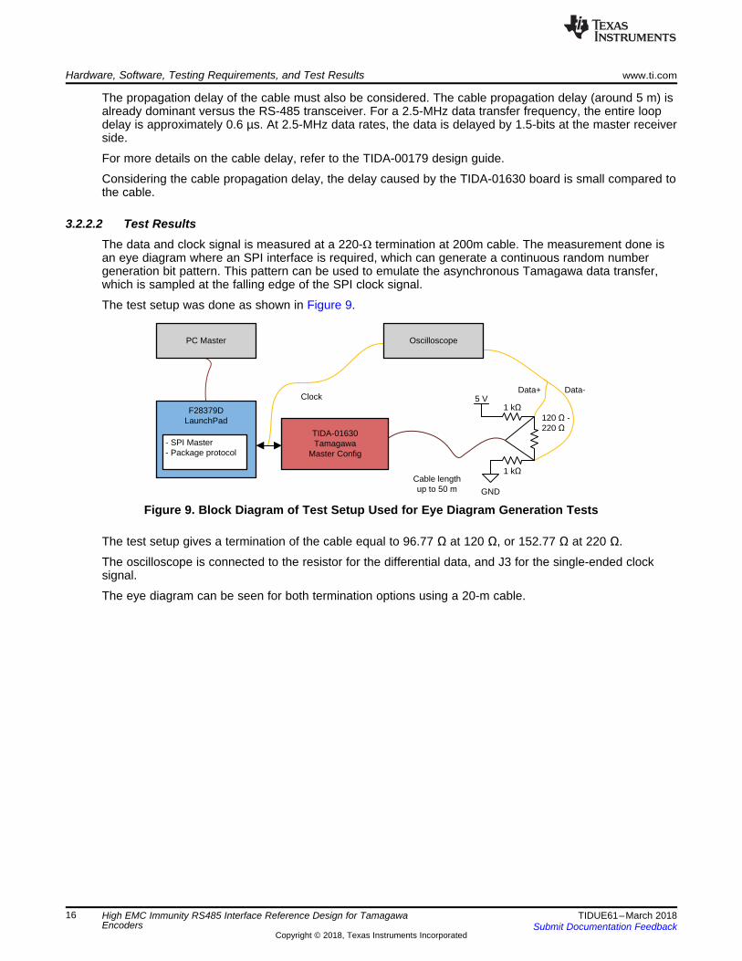
3.2.2.2 Test ResultsThe data and clock signal is measured at a 220-Ω termination at 200m cable. The measurement done isan eye diagram where an SPI interface is required, which can generate a continuous random numbergeneration bit pattern. This pattern can be used to emulate the asynchronous Tamagawa data transfer,which is sampled at the falling edge of the SPI clock signal.
The test setup was done as shown in Figure 9.
Figure 9. Block Diagram of Test Setup Used for Eye Diagram Generation Tests
The test setup gives a termination of the cable equal to 96.77 Ω at 120 Ω, or 152.77 Ω at 220 Ω.
The oscilloscope is connected to the resistor for the differential data, and J3 for the single-ended clocksignal.
The eye diagram can be seen for both termination options using a 20-m cable.
High EMC Immunity RS485 Interface Reference Design for TamagawaEncoders
Figure 10. Eye Diagram of the THVD1550 at Master Transmit, 20-m Cable Data Rate 2.5 MHz With 220-ΩTermination
During these tests, it was seen that the choice of 220-Ω termination gives a poor eye diagram for industrialgrade cables; the use of a 120-Ω termination on the drive side gives a better eye while using the cable inthis report. The eye performance can be accepted if the cable length is limited in such a way that thetermination ringing does not effect the measurement point. If this is done, this increases the common-mode voltage of the receiver signal. This gives the receiver a larger voltage difference to detect themeasured signal.
High EMC Immunity RS485 Interface Reference Design for TamagawaEncoders
Figure 11. Eye Diagram of the THVD1550 at Master Transmit, 20-m Cable Data Rate 2.5 MHz with 120-ΩTermination
The jitter of the received differential data at the cable with a 120-Ω termination at the Tamagawafrequency is around 5% (0.95 UI-open). The steady state differential voltage is around ±2.5 V (5.0 Vpp).However, the rise or fall time from 10% to 90% is half a clock cycle. Taking into account that the receivedata is sampled at the falling clock edge (in the center of the clock cycle), the effective worst casedifferential voltage is approximately ±2.3 V. Because Tamagawa specifies the data frequency based on a50% duty cycle, the data frequency can be supported.
3.2.2.3 System PerformanceTests are done using the interface as an encoder interface; in this case, the Tamagawa T-Format protocolis used combined with an Tamagawa encoder.
The T-Format master interface is a known RS485 transceiver, and Tamagawa Slave (Encoder) is anunknown transceiver.
3.2.2.3.1 Tamagawa TestsThe test uses the TS5667N422 encoder. Figure 12 shows the block diagram of the test setup.
High EMC Immunity RS485 Interface Reference Design for TamagawaEncoders
3.2.2.4.2 Power-down Behavior of the On-board Supply
Figure 16. Power Down Sequence of the TIDA-01630
During power down, the 5-V rail and the encoder voltage start ramping down as the 3v3 rail gets below2.7 V, as expected.
3.2.2.4.3 Power Consumption of the SystemFor the test of the power consumption measurement, the following test setup was done. Power to theLaunchPad was provided over the USB connection from the PC master.
Figure 17. Block Diagram of Test Setup for the Power Consumption Tests
For this measurement, current was measured after disabling the 5-V boost and converted pulling theenable pin to ground, removing the resistor R2 externally powering the LaunchPad.
The power consumption is measured with the TIDA-01630 running a Tamagawa encoder at 2.5-MHz clockfrequency, with a communication repetition of 16 kHz. The termination is 120 Ω with 1k parallel and a 20-m cable.
High EMC Immunity RS485 Interface Reference Design for TamagawaEncoders
Table 10. Power Consumption for 5 V and 3v3 Rail at 220-Ω Termination
Measurement Task 5-V Boost 3v3 Buck 5-V EncoderCurrent[mA] Idle 3.33 mA 0.51 mA 67.3 mACurrent[mA] Tamagawa at 2.5 MHz 7.38 mA 0.54 mA 80.6 mA
3.2.2.5 EMC Immunity Test ResultsThe TIDA-01630 TI design has been tested for IEC61000-4-4 and 4-5 (EFT and Surge), with test levelsand performance criterion specified in the standard IEC 61800-3 “EMC immunity requirements andspecific test methods applicable in adjustable speed, electrical-power drive systems”.
The design meets these standards and exceeds the voltage levels.
Table 11. IEC618000-3 EMC Immunity Requirements for Second Environment and MeasuredVoltage Levels and Class
IEC61000-4-5 ±1 kV.Becauseshielded cable> 20 m, directcoupling toshield (2 Ω /500 A)
B ±2 kV A PASS(EXCEED)
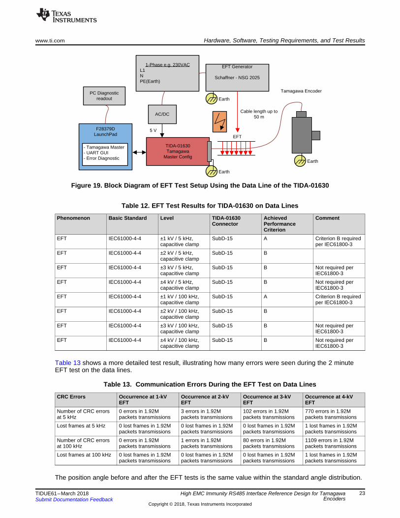
3.2.2.5.1 IEC-61000-4-4 Electrical Fast Transient (EFT) Test ResultsA diagram and a picture of the EFT test setup for TIDA-01630 is shown in Figure 18 and Figure 19.During the test, the SubD-15 female connector is connected to the encoder by using a 20-m cable.
Figure 18. Picture of EFT Test Setup for Data Line of the TIDA-01630
High EMC Immunity RS485 Interface Reference Design for TamagawaEncoders
3.2.2.5.2 IEC-61000-4-5 Surge Test ResultsA diagram and a picture of the EFT test setup for the TIDA-01630 is shown in Figure 21 and Figure 20.During the test, the SubD-15 female connector is connected to the encoder by using a 20-m cable.
Figure 20. Picture of Surge Test Setup for TIDA-01630
High EMC Immunity RS485 Interface Reference Design for TamagawaEncoders
4.4 Altium ProjectTo download the Altium Designer® project files, see the design files at TIDA-01630 .
4.5 Gerber FilesTo download the Gerber files, see the design files at TIDA-01630 .
4.6 Assembly DrawingsTo download the assembly drawings, see the design files at TIDA-01630 .
5 Software FilesTo download the software files, see the design files at ControlSuite .
6 Related Documentation
1. Universal Digital Interface to Absolute Position Encoders Reference Design2. C2000™ Position Manager T-Format Library Module3. DesignDRIVE Development Kit IDDK v2.2.1
6.1 TrademarksE2E, BoosterPack, LaunchPad, C2000, DCS-Control, Code Composer Studio are trademarks of TexasInstruments.Agilent is a trademark of Agilent Technologies, Inc..Altium Designer is a registered trademark of Altium LLC or its affiliated companies.Mitsubishi is a trademark of Mitsubishi Shoji Kaisha, Ltd.PROFIBUS is a registered trademark of PROFIBUS and PROFINET International (PI).Tamagawa is a trademark of Tamagawa Seiki Co., Ltd..BiSS is a registered trademark of iC-Haus GmbH..All other trademarks are the property of their respective owners.
7 TerminologyEFT - Electrical Fast Transient
8 About the AuthorKRISTEN MOGENSEN is a system engineer in the Industrial Systems-Motor Drive team at TexasInstruments, responsible for developing reference designs for industrial drives.
MARTIN STAEBLER is a system architect in the Industrial Systems-Motor Drive team at TexasInstruments, responsible for specifying and developing reference designs for industrial drives.
IMPORTANT NOTICE FOR TI DESIGN INFORMATION AND RESOURCES
Texas Instruments Incorporated (‘TI”) technical, application or other design advice, services or information, including, but not limited to,reference designs and materials relating to evaluation modules, (collectively, “TI Resources”) are intended to assist designers who aredeveloping applications that incorporate TI products; by downloading, accessing or using any particular TI Resource in any way, you(individually or, if you are acting on behalf of a company, your company) agree to use it solely for this purpose and subject to the terms ofthis Notice.TI’s provision of TI Resources does not expand or otherwise alter TI’s applicable published warranties or warranty disclaimers for TIproducts, and no additional obligations or liabilities arise from TI providing such TI Resources. TI reserves the right to make corrections,enhancements, improvements and other changes to its TI Resources.You understand and agree that you remain responsible for using your independent analysis, evaluation and judgment in designing yourapplications and that you have full and exclusive responsibility to assure the safety of your applications and compliance of your applications(and of all TI products used in or for your applications) with all applicable regulations, laws and other applicable requirements. Yourepresent that, with respect to your applications, you have all the necessary expertise to create and implement safeguards that (1)anticipate dangerous consequences of failures, (2) monitor failures and their consequences, and (3) lessen the likelihood of failures thatmight cause harm and take appropriate actions. You agree that prior to using or distributing any applications that include TI products, youwill thoroughly test such applications and the functionality of such TI products as used in such applications. TI has not conducted anytesting other than that specifically described in the published documentation for a particular TI Resource.You are authorized to use, copy and modify any individual TI Resource only in connection with the development of applications that includethe TI product(s) identified in such TI Resource. NO OTHER LICENSE, EXPRESS OR IMPLIED, BY ESTOPPEL OR OTHERWISE TOANY OTHER TI INTELLECTUAL PROPERTY RIGHT, AND NO LICENSE TO ANY TECHNOLOGY OR INTELLECTUAL PROPERTYRIGHT OF TI OR ANY THIRD PARTY IS GRANTED HEREIN, including but not limited to any patent right, copyright, mask work right, orother intellectual property right relating to any combination, machine, or process in which TI products or services are used. Informationregarding or referencing third-party products or services does not constitute a license to use such products or services, or a warranty orendorsement thereof. Use of TI Resources may require a license from a third party under the patents or other intellectual property of thethird party, or a license from TI under the patents or other intellectual property of TI.TI RESOURCES ARE PROVIDED “AS IS” AND WITH ALL FAULTS. TI DISCLAIMS ALL OTHER WARRANTIES ORREPRESENTATIONS, EXPRESS OR IMPLIED, REGARDING TI RESOURCES OR USE THEREOF, INCLUDING BUT NOT LIMITED TOACCURACY OR COMPLETENESS, TITLE, ANY EPIDEMIC FAILURE WARRANTY AND ANY IMPLIED WARRANTIES OFMERCHANTABILITY, FITNESS FOR A PARTICULAR PURPOSE, AND NON-INFRINGEMENT OF ANY THIRD PARTY INTELLECTUALPROPERTY RIGHTS.TI SHALL NOT BE LIABLE FOR AND SHALL NOT DEFEND OR INDEMNIFY YOU AGAINST ANY CLAIM, INCLUDING BUT NOTLIMITED TO ANY INFRINGEMENT CLAIM THAT RELATES TO OR IS BASED ON ANY COMBINATION OF PRODUCTS EVEN IFDESCRIBED IN TI RESOURCES OR OTHERWISE. IN NO EVENT SHALL TI BE LIABLE FOR ANY ACTUAL, DIRECT, SPECIAL,COLLATERAL, INDIRECT, PUNITIVE, INCIDENTAL, CONSEQUENTIAL OR EXEMPLARY DAMAGES IN CONNECTION WITH ORARISING OUT OF TI RESOURCES OR USE THEREOF, AND REGARDLESS OF WHETHER TI HAS BEEN ADVISED OF THEPOSSIBILITY OF SUCH DAMAGES.You agree to fully indemnify TI and its representatives against any damages, costs, losses, and/or liabilities arising out of your non-compliance with the terms and provisions of this Notice.This Notice applies to TI Resources. Additional terms apply to the use and purchase of certain types of materials, TI products and services.These include; without limitation, TI’s standard terms for semiconductor products http://www.ti.com/sc/docs/stdterms.htm), evaluationmodules, and samples (http://www.ti.com/sc/docs/sampterms.htm).