IEEE TRANSACTIONS ON ELECTRON DEVICES, VOL 40, NO 8, AUGUST 1993 1437 High-Field Breakdown in Thin Oxides Grown in N20 Ambient Aniruddha B. Joshi, Giwan Yoon, Jonghan Kim, G. Q. Lo, and Dim-Lee Kwong Abstract-We report a detailed study of time-dependent di- electric breakdown (TDDB) in N20-grpwn thin (47-120 A) ox- ides. A significant degradation in breakdown properties (such as charge-to-breakdown, breakdown field) was observed in N20 oxides with increasing oxide growth temperature; a strikingly different dependence than that in pure oxides. A physical model based on undulations at the Si/Si02 interface is discussed to account for the degradation of breakdown properties for higher N20 oxidation temperature. Accelerated breakdown in N20 ox- ides for higher operating temperatures and higher oxide fields as well as thickness dependence of TDDB are studied under both polarities of injection. These dependencies are similar to the reported data on pure oxides. Breakdown under unipolar and bipolar stress in N20 oxides is compared with dc break- down. Unlike the case of pure oxides, an asymmetric improve- ment in time-to-breakdown under positive versus negative gate unipolar stress is observed, which is attributed to charge de- trapping behavior in N20 oxides. A dramatic reduction in time- to-breakdown of N20 oxide is observed under bipolar stress when the thickness is scaled below 60 A. A physical model, based on the thickness dependence of trapped hole centroid, is suggested to explain this behavior. Overall, our results indicate that N20 oxides are expected to show improved breakdown properties than pure Si02 over a wide range of operating tem- peratures, electric fields, oxide thicknesses, as well as under ac stress. I. INTRODUCTION OR THE past decade, considerable work has been F reported on alternative gate dielectrics for submi- crometer MOS devices in ULSI applications. Oxynitrides are the most extensively studied alternative gate dielec- trics [1]-[13]. A variety of methods such as reoxidation of NH3-nitrided Si02 [1]-[4], N 2 0 oxidations of Si [5]- [8], N20 nitridation of thermal [9]-[ll] and CVD [12] oxides, and nitrogen implant through polysilicon gate [ 131 have been used to fabricate nitrided gate oxides. N20- based approaches appear to be more promising than NH3 nitridation of Si02 due to the hydrogen-free nature of pro- cessing. Incorporation of hydrogen in oxide during NH3 Manuscript received August 27, 1992; revised January 11, 1993. This work was supported by SRCEEMATECH under Contract 91MC505 and by the Texas Advanced Technology Program. The review of this paper was arranged by Associate Editor Y. Nishi. A. B. Joshi was with the Microelectronics Research Center, Department of Electrical and Computer Engineering, The University of Texas at Aus- tin, Austin, TX 78712. He is now with Rockwell International, Newport Beach, CA. G. Yoon, J. Kim, G. Q. Lo, and D. L. Kwong are with the Microelec- tronics Research Center, Department of Electrical and Computer Engi- neering, The University of Texas at Austin, Austin, TX 78712. IEEE Log Number 9208728. nitridation necessitates an additional reoxidation /N2 an- nealing step to reduce electron trapping in nitrided oxides [3], [4]. Other advantages of N20-based approaches to fabricate oxynitride gate dielectrics include excellent per- formance and reliability of the resulting devices, good thickness control, and simplicity of the process. Performance and reliability of N 2 0 oxides (i.e., oxides growth in N20 ambient) have been investigated in detail [5]-[S]. These oxides show reduced electron and hole trapping, superior breakdown properties, and suppressed interface state generation under hot-carrier stress, as com- pared to pure Si02. Furthermore, no significant increase in fixed charge or interface-state density is observed in these oxides as is usually reported for NH3 nitridation of Si02 [2]. MOSFET’s with N 2 0 gate oxides show slightly higher electron and hole effective mobilities [7], [8]. De- spite such a considerable effort on N20 oxides, little at- tention has been given to the high-field breakdown in these oxides. Such investigation is necessary prior to imple- menting N 2 0 oxides in such applications as dielectrics for nonvolatile memories. Moreover, dependence of N20 breakbown properties on the processing conditions, spe- cifically the oxide growth temperature, is an important is- siie, as yet unexplored. In this work, we focus our attention on several aspects related to high-field stress-induced breakdown in N 2 0 ox- ides. The specific aspects which will be addressed in this work are: dependence of time-dependent dielectric break- down (TDDB) characteristics on growth temperature, temperature and field acceleration of breakdown, impact of oxide thickness scaling on breakdown, and breakdown under unipolar and bipolar stress. We have observed that some of the trends investigated are modified as compared to the ones in pure Si02; nitrogen-rich Si/Si02 interface in N20 oxides being responsible for these modifications. Results indicate that N 2 0 oxides are expected to show su- perior breakdown properties than pure Si02 over a wide range of operating temperatures, electric fields, oxide thicknesses, and under ac stress. 11. EXPERIMENTAL An etch-back process with 4000- A field oxide was used to fabricate MOS capacitors on 3-5 Q cm (100) p-type Si wafers. Piranha cleaning was performed before steam field oxidation at 900°C. Photolithography and chemical etch were used to define the active areas. Standard RCA cleaning was performed prior to gate oxidation and the 0018-9383/93$03.00 0 1993 IEEE
Transcript
IEEE TRANSACTIONS ON ELECTRON DEVICES, VOL 40, NO 8, AUGUST 1993 1437
High-Field Breakdown in Thin Oxides Grown in N20 Ambient
Aniruddha B. Joshi, Giwan Yoon, Jonghan Kim, G. Q. Lo, and Dim-Lee Kwong
Abstract-We report a detailed study of time-dependent di- electric breakdown (TDDB) in N20-grpwn thin (47-120 A) ox- ides. A significant degradation in breakdown properties (such as charge-to-breakdown, breakdown field) was observed in N20 oxides with increasing oxide growth temperature; a strikingly different dependence than that in pure oxides. A physical model based on undulations at the Si/Si02 interface is discussed to account for the degradation of breakdown properties for higher N 2 0 oxidation temperature. Accelerated breakdown in N 2 0 ox- ides for higher operating temperatures and higher oxide fields as well as thickness dependence of TDDB are studied under both polarities of injection. These dependencies are similar to the reported data on pure oxides. Breakdown under unipolar and bipolar stress in N20 oxides is compared with dc break- down. Unlike the case of pure oxides, an asymmetric improve- ment in time-to-breakdown under positive versus negative gate unipolar stress is observed, which is attributed to charge de- trapping behavior in N20 oxides. A dramatic reduction in time- to-breakdown of N20 oxide is observed under bipolar stress when the thickness is scaled below 60 A. A physical model, based on the thickness dependence of trapped hole centroid, is suggested to explain this behavior. Overall, our results indicate that N 2 0 oxides are expected to show improved breakdown properties than pure Si02 over a wide range of operating tem- peratures, electric fields, oxide thicknesses, as well as under ac stress.
I. INTRODUCTION OR THE past decade, considerable work has been F reported on alternative gate dielectrics for submi-
crometer MOS devices in ULSI applications. Oxynitrides are the most extensively studied alternative gate dielec- trics [1]-[13]. A variety of methods such as reoxidation of NH3-nitrided Si02 [1]-[4], N 2 0 oxidations of Si [5]- [8], N20 nitridation of thermal [9]-[ll] and CVD [12] oxides, and nitrogen implant through polysilicon gate [ 131 have been used to fabricate nitrided gate oxides. N20- based approaches appear to be more promising than NH3 nitridation of Si02 due to the hydrogen-free nature of pro- cessing. Incorporation of hydrogen in oxide during NH3
Manuscript received August 27, 1992; revised January 11, 1993. This work was supported by SRCEEMATECH under Contract 91MC505 and by the Texas Advanced Technology Program. The review of this paper was arranged by Associate Editor Y. Nishi.
A. B. Joshi was with the Microelectronics Research Center, Department of Electrical and Computer Engineering, The University of Texas at Aus- tin, Austin, TX 78712. He is now with Rockwell International, Newport Beach, CA.
G. Yoon, J. Kim, G. Q . Lo, and D. L. Kwong are with the Microelec- tronics Research Center, Department of Electrical and Computer Engi- neering, The University of Texas at Austin, Austin, TX 78712.
IEEE Log Number 9208728.
nitridation necessitates an additional reoxidation /N2 an- nealing step to reduce electron trapping in nitrided oxides [3], [4]. Other advantages of N20-based approaches to fabricate oxynitride gate dielectrics include excellent per- formance and reliability of the resulting devices, good thickness control, and simplicity of the process.
Performance and reliability of N 2 0 oxides (i.e., oxides growth in N20 ambient) have been investigated in detail [ 5 ] - [ S ] . These oxides show reduced electron and hole trapping, superior breakdown properties, and suppressed interface state generation under hot-carrier stress, as com- pared to pure Si02. Furthermore, no significant increase in fixed charge or interface-state density is observed in these oxides as is usually reported for NH3 nitridation of Si02 [2]. MOSFET’s with N 2 0 gate oxides show slightly higher electron and hole effective mobilities [7], [8]. De- spite such a considerable effort on N 2 0 oxides, little at- tention has been given to the high-field breakdown in these oxides. Such investigation is necessary prior to imple- menting N 2 0 oxides in such applications as dielectrics for nonvolatile memories. Moreover, dependence of N 2 0 breakbown properties on the processing conditions, spe- cifically the oxide growth temperature, is an important is- siie, as yet unexplored.
In this work, we focus our attention on several aspects related to high-field stress-induced breakdown in N 2 0 ox- ides. The specific aspects which will be addressed in this work are: dependence of time-dependent dielectric break- down (TDDB) characteristics on growth temperature, temperature and field acceleration of breakdown, impact of oxide thickness scaling on breakdown, and breakdown under unipolar and bipolar stress. We have observed that some of the trends investigated are modified as compared to the ones in pure Si02; nitrogen-rich Si/Si02 interface in N 2 0 oxides being responsible for these modifications. Results indicate that N 2 0 oxides are expected to show su- perior breakdown properties than pure Si02 over a wide range of operating temperatures, electric fields, oxide thicknesses, and under ac stress.
11. EXPERIMENTAL An etch-back process with 4000- A field oxide was used
to fabricate MOS capacitors on 3-5 Q cm (100) p-type Si wafers. Piranha cleaning was performed before steam field oxidation at 900°C. Photolithography and chemical etch were used to define the active areas. Standard RCA cleaning was performed prior to gate oxidation and the
0018-9383/93$03.00 0 1993 IEEE
1438
I
IEEE TRANSACTIONS ON ELECTRON DEVICES, VOL. 40, NO. 8, AUGUST 1993
wafers were transferred immediately to a conventional re- sistance-heated furnace. The furnace temperature was ramped up from 750°C to the oxidation temperature (950- 1050°C) in a mixture of nitrogen and low-flow ( -2%) oxygen to avoid the possibility of Si3N4 formation during ramp-up in pure N2. After reaching the oxidation temper- ature, N 2 0 was introduced into the furnace and gate oxi- dation was performed for different durationso to grow ox- ides in the thickness range of 47 to 120 +. For com- parison, pure SiO, with a thickness of 115 A was grown in pure 0, ambient at different temperatures (950- 1050°C). In situ post-oxidation annealing at the oxidation temper- ature followed by the temperature ramg-down were per- formed in N2 ambient. After -3500-A polysilicon gate deposition and P0Cl3 doping, a second lithography step, reactive ion etching and forming gas anneal were per- formed to fabricate n+-polysilicon gated MOS capacitors. Gate dielectric thicknesses measured by ellipsometry (re- fractive index = 1.462) and C-V measurements (eox = 3 . 9 ~ ~ ) were in good agreement with each other. Capaci- tors with gate areas ranging from 5 x lop5 to 1 X lop2 were used in this work.
111. RESULTS AND DISCUSSION A. Initial Properties of MOS Capacitors
Fig. 1 shows fixed charge (Nf) and midgap interface state density (D;, - ,,J in N 2 0 oxides with different thick- nesses. It is observed that both these quantities show a systematic increase with increase in oxide thickness. It has been reported that these quantitie! increase as the thickness is reduced from 1000 to 350 A [14] in conven- tional SiO,. This observation was attributed to higher ox- idation rate in the initial stages of oxidation. Hahn and Henzler [ 151 demonstrated an excellent correlation be- tween interface roughness and N' and D , . It was further $own that with reduction in oxide thickness below 200 A , interface roughness increpses initially and then re- mains constant below - 100 A . Consequently, a similar thickness dependence can be assumed for conventional SiO,. Thus the thickness dependence of Nf and D;, in N 2 0 oxides (Fig. 1) is different from that in conventional S O 2 . It is known that the oxide growth in N 2 0 is significantly slower due to the buildup of nitrogen-rich layer at the Si/Si02 interface, suppressing diffusion of the oxidant to the interface [ 161. Thus N' and D , formation in N 2 0 ox- ides is likely to be dominated by an alternative mecha- nism. We believe that nitrogen at the Si /Si02 interface plays a significant role in controlling Nf and Di, in N20 oxides.
A paramagnetic bridging nitrogen center was observed in NH,-nitrided S O 2 , which was rendered diamagnetic by electron injection, suggesting that this center acts as a dominant electron trap in these films [17]. Since electron trapping is substantially smaller in N20 oxides as com- pared to pure SiO, [5], the presence of such nonbridging center is unlikely in N 2 0 oxides. On the other hand, Stathis et al. [18] reported the presence of E' centers
40 60 80 100 120 140 Oxide Thickness (A)
Fig. 1 . Fixed charge and midgap interface state density in N 2 0 oxides (growth temperature: 950°C) with various thicknesses.
(positive oxygen vacancies) and fourfold coordinated ni- trogen in plasma-enhanced chemical vapor deposited films using SiH4 and N20. Probably a similar defect is gener- ated during N 2 0 oxidation, which results in an increase in Nf and D,. As postulated in a model for NH3-nitrida- tion-induced Nf and Dj, [2], the spatial location of a nitro- gen-related defect decides whether it results in Nf or Dit.
Current density (J,) versus electric field (Eox) curves were obtained by voltage ramping technique. Identical slopes in the Fowler-Nordheim (F-N) tunneling regime indicated that the barrier height for electron injection in N20 oxides is identical to that in pure SiO,.
B. Dependence of Breakdown Properties on Oxide Growth Temperature
Time-zero breakdown (TZB) of N 2 0 oxides grown at different temperatures was investigated. The destructive breakdown field decreased by - 2 MV/cm as the growth temperature increased from 950°C to 1050°C. However, there was no significant change in the number of A-mode low-field breakdowns, suggesting that the increase in growth temperature had no significant effect on the den- sity of pinholes.
Fig. 2 shows the dependence of charge-to-breakdown Qbd (to 50% cumulative failure) under constant current stress on the oxide growth temperature for MOS capaci- tors with N 2 0 and control oxides. Although Qbd for N 2 0 oxide growth at 950°C is much larger than that for control oxide, Qbd for N 2 0 oxides drastically reduces with in- creasing growth temperature whereas that for the control oxide increases slightly. Consequently, at 1050°C growth temperature, control oxides show 16x larger Qbd than N 2 0 oxides. Similar trends are observed for time-to- breakdown (tbd) under constant voltage stress as shown in Fig. 3 . For the range of electric fields investigated, severe degradation of tbd is observed by increasing the growth temperature in N20 ambient. In control oxides, on the other hand, tbd shows very little dependence on the growth temperature.
Several researchers have attributed reduction in Qbd [ 191 and breakdown field [ 191-[21] in SiO, to electric field in- tensification at local thin oxide spots. Fukuda et al. [ 101 reported a significant reduction in Qbd and tbd whenever RTP in N20 was followed by RTP in Oz. This reduction
I I
1439 JOSH1 er al.: HIGH-FIELD BREAKDOWN IN THIN OXIDES
102
900 950 IO00 1050 1100 Growth Temperature ("C)
0 5 10 15 20 25 30 Effective Oxide Thinning (A)
Fig. 2. Charge-to-breakdown (for 50% failure) for pure and N 2 0 oxides grown at different temperatures under a constant current stress of - 100 mA/cm* The oxide thickness was 115 A and 0.005-cm2 capacitors were used.
Fig. 4. Defect density versus effective oxide thinning for N20 oxides. The data are calculated from tM distributions at E,, = - 11.1 MV/cm, by fol- lowing an approach similar to that in [18].
h
v
resulted in the best breakdown properties in N20 oxides, a trend strikingly different from that in pure SO2 . There- fore, the subsequent studies on different aspects of dielec- tric breakdown were performed on N20 oxides grown at 950°C.
C. Temperature Acceleration of Breakdown Temperature dependence of breakdown was studied in
N 2 0 oxides under gate and substrate injection over a wide 7.5 8 8.5 9 9.5 10 range of temperatures (25-300°C). A significant reduc-
tion in tbd was observed with increasing the temperature.
to 30O0C, fbd decreased from 614 to 5 s under gate injec-
- 1 h X (XI@ cmN) Fig. 3. Time-to-breakdown plots for 115-A pure and N 2 0 oxides grown at 950°C and 1050°C under gate injection at different electric fields. The For with an increase in temperature from 550c capacitor area was 0.005 cm'.
was attributed to large undulations at the Si/Si02 inter- face, observed by high-resolution TEM measurements, which resulted in localized high electric fields leading to smaller Qbd. The mechanism of formation of the undula- tions, however, was not explained.
We investigated such thin spots/undulations in N 2 0 ox- ides by using an approach similar to that adopted by Tan- aka et al. [22]. In this approach, the differences between tbd for early failures and fbd-l@)% (fbd for 100% failure) in a sample are translated into effective oxide thinning (AX) whereas the failure rate is an indicator of the density of thin oxide spots. Fig. 4 shows AX for N 2 0 oxides grown at 950°C and 1050°C and the density of thin oxide spots, obtained by following tbe procedure in [22]. Maximum oxide thinning is - 10 A for N 2 0 oxide grown at 950°C and increased to -25 A for N 2 0 oxide grown at 1050°C.
Excessive nitrogen incorporation at the Si/Si02 inter- face during N20 oxidation may be responsible for the large oxide thinning in N20 oxides grown at higher tempera- tures. Since nitrogen presents a strong barrier to oxidant diffusion [23], the oxidation rate is locally retarded at such nitrogen-rich areas, leading to an inhomogeneous oxide growth. Electric field intensification at the locally thin ox- ide spots leads to degradation of breakdown properties, as observed in Figs. 2 and 3. It is interesting to note that the same model can account for the large undulations at the Si/Si02 interface in oxides in [lo], grown by RTP in N20 followed by RTP in Oz.
Thus the lowest growth temperature studied (950°C)
tion and from 5060 to 30 s under substrate injection. Tem- perature acceleration of breakdown in pure oxides has been studied in detail previously [24], [25]. Chen et al. [24] concluded that the enhanced rate of electron trap gen- eration with increasing temperature is the main process responsible for the accelerated breakdown at elevated op- erating temperatures.
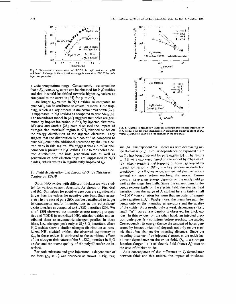
Similar to pure oxides, time-to-breakdown in N 2 0 ox- ides shows a dependence of the form & a exp (Erbd/kT) on operating temperature, where Erbd is activation energy for tbd. A significant change in the activation energy was observed at - 150°C as shown in Fig. 5 . This result is similar to the reported results for pure oxides [24], [25] as well as to a recent work on reoxidized NH3-nitrided oxides [26]. The values for Erbd are 0.21 and 0.43 eV for substrate injection and 0.18 and 0.32 eV for gate injection for low- and high-temperature regions (separated at - 150"C), respectively.
A wide range of Erbd values has been reported in the literature and it is believed that the differences are mainly due to differences in the quality of the oxides and different applied electric fields [25]. A model was presented in [25], according to which activation energy can be obtained as a universal function of tbd. For example, larger activation energy is obtained for high-quality oxide and/or low-field stressing, both of which lead to longer fbd. Using the ac- tivation energy values for the N 2 0 oxides, we obtained fbd values for various temperatures using the universal curve for pure SiOz [25]. These values were significantly smaller than the fbd values for N20 oxides shown in Fig. 5, over
r
1440 IEEE TRANSACTIONS ON ELECTRON DEVICES, VOL. 40, NO. 8, AUGUST 1993
104 " ' ' I ' " ' 1 ' ' ' ' l ~ ~ o ~ 2 1 ' e v ,
I=.
1 1.5 2 2.5 3 3.5 4 1OOOE ( IPK)
Fig. 5 . Temperature acceleration of TDDB in N20 oxides at +20 mA/cm2. A change in the activation energy is seen at - 150" C for both injection polarities.
a wide temperature range. Consequently, we speculate that a Etbd versus tbd curve can be obtained for N20 oxides and that it would be shifted towards higher tbd values as compared to the curve in [25] for pure Si02.
The longer tbd values in N 2 0 oxides as compared to pure Si02 can be attributed to several reasons. Hole trap- ping, which is a key process in dielectric breakdown [27], is suppressed in N 2 0 oxides as compared to pure Si02 [6]. The breakdown model in [27] suggests that holes are gen- erated by impact ionization in Si02 by injected electrons. DiMaria and Stathis [28] have discussed the impact of nitrogen-rich interfacial region in NH3-nitrided oxides on the energy distribution of the injected electrons. They suggest that the distribution is "cooler" as compared to pure Si02 due to the additional scattering by shallow elec- tron traps in this region. We suggest that a similar phe- nomenon is present in N 2 0 oxides. Due to the cooler elec- tron distribution, the hole generation rate as well as generation of new electron traps are suppressed in N 2 0 oxides, which results in significantly improved tbd.
D. Field Acceleration and Impact of Oxide Thickness Scaling on TDDB
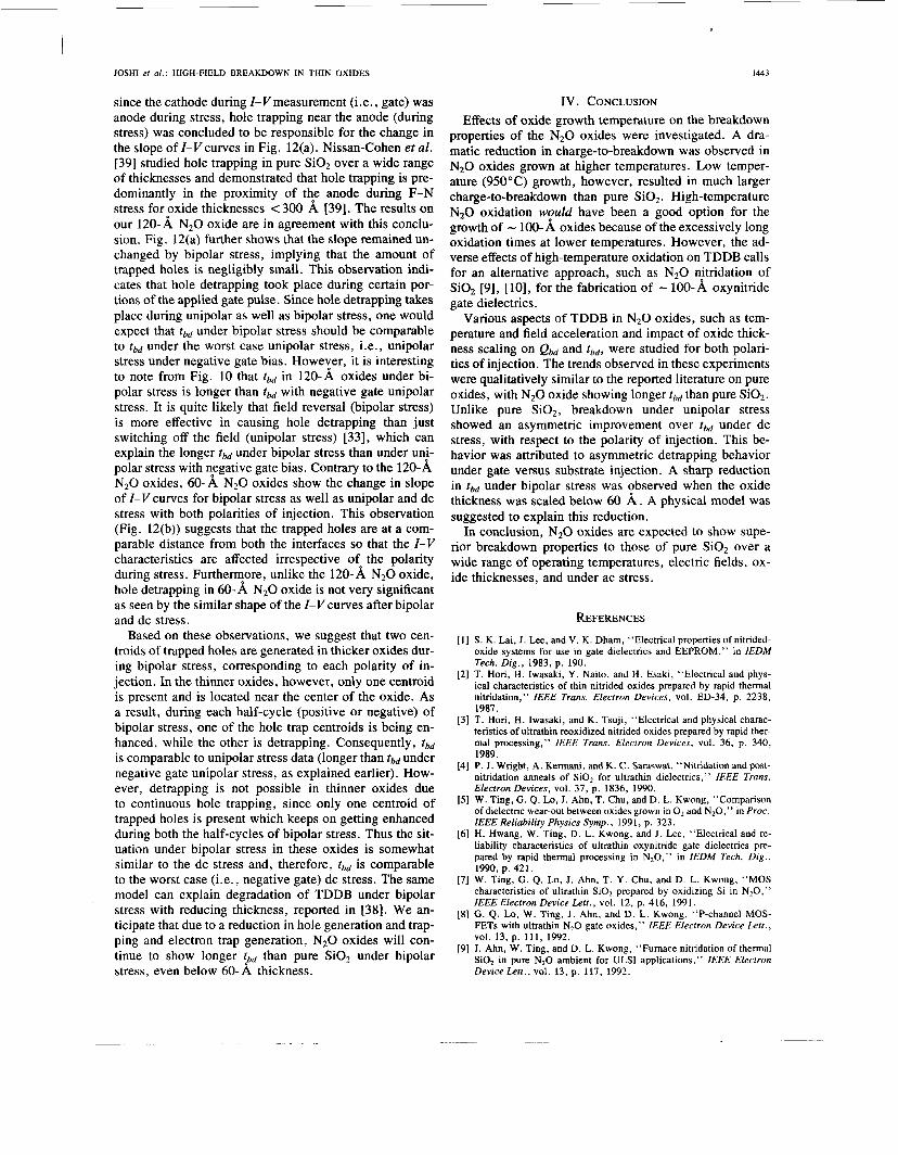
Qbd in N 2 0 oxides with different thicknesses was stud- ied for various current densities. As shown in Fig. 6(a) and (b), Qbd values for positive gate bias are significantly larger than the values for negative gate bias. Such asym- metry in the case of pure Si02 has been attributed to larger inhomogeneity and/or imperfections at the polysilicon/ oxide interface as compared to Si/Si02 interface [29]. Wu et al. [30] observed asymmetric charge trapping proper- ties and TDDB in reoxidized NH3-nitrided oxides and at- tributed them to asymmetric nitrogen profiles in these films, i.e., nitrogen peak only at Si/Si02 interface. Since N 2 0 oxides show a similar nitrogen distribution as reox- idized NH,-nitrided oxides, the observed asymmetry in Qbd in these oxides is attributed to the combined effects of the nitrogen-rich nature of the Si/Si02 interface in N 2 0 oxides and the worse quality of the polysilicon/oxide in- terface.
For both substrate and gate injections, a dependence of the form Qbd ot J i was observed as shown in Fig. 6(a)
103 m- E -L? U e g 4 102 e n
3 i? 8
IO'
T_m_r ' ' ' " " ' I
N 2 0 Oxides I Growth @ 950°C Substrate Injection
I , I.i,d 102 1 03
J~ (mA/cm2)
(a)
Gate Injection
10' " " ' ~ ~ 1 ' '
102 103 - J ~ (mA/cm2)
(b) Fig. 6. Charge-to-breakdown under (a) substrate and (b) gate injection for NzO oxides with different thicknesses. A significant change in slope of Qbd
versus J , curves is seen with the changes in the thickness.
and (b). The exponent "n" increases with decreasing ox- ide thickness (Tax). Similar dependence of exponent "n" on To, has been observed for pure oxides [3 13. The results in [3 11 were explained based on the model by Chen et al . [27] which suggests that trapping of holes, generated by impact ionization in Si02, is a key process in dielectric breakdown. In a thicker oxide, an injected electron suffers several collisions before reaching the anode. Conse- quently, its average energy depends on the oxide field as well as the mean free path. Since the current density de- pends exponentially on the electric field, the electric field variation over the range of J g studied here is fairly small ( - 2 MV/cm variation for more than an order of magni- tude variation in J g ) . Furthermore, the mean free path de- pends only on the operating temperature and the quality of the oxide. As a result, only a weak dependence (i.e., small "n") on current density is observed for thick ox- ides. In thin oxides, on the other hand, an injected elec- tron undergoes few collisions before reaching the anode. Consequently, its energy (hence the amount of holes gen- erated by impact ionization) depends not only on the elec- tric field, but also on the traveling distance. Since the traveling distance of an injected electron in the oxide has a linear dependence on the oxide field, Qbd is a stronger function (larger "n") of electric field (hence Jg) than in the case of thicker oxides.
As a consequence of this difference in J g dependence between thick and thin oxides, the impact of thickness
JOSH1 et al.: HIGH-FIELD BREAKDOWN IN THIN OXIDES 1441
- Gate Injection '
40 60 80 100 120 140 Oxide Thickness (A)
Fig. 7 . Charge-to-breakdown versus oxide thickness under substrate and gate injection for NzO oxides at different current densities, obtained from Fig. 5 .
scaling is different for different current densities. As shown in Fig. 7, Qbd monotonically increases with reduc- tion in thickness for a lower current dps i ty (100 mA/cm2), while it shows a minima near 90 A at a higher current density of (500 mA/cm2). These observations are consistent with the trends reported in [31] for pure S O 2 . For still higher current densities, a monotonic decrease in Qbd with reduced thickness is expected.
TDDB under constant voltage stress was studied in N 2 0 oxides. Under both gate and substrate injection, a depen- dence of the form tbd oc exp ( (B + H)/E,,) was observed as shown in Fig. 8(a) and (b). This dependence is con- sistent with the hole trapping model of dielectric break- down [27]. It can be seen from this figure that slopes of tbd versus E,' curves depend on the dielectric thickness and that thicker oxides have a steeper dependence on E::. Such dependence of field acceleration on oxide thickness has been reported for dry as well as wet oxides
As observed from Fig. 8(a) and (b), tbd monotonically decreases with reduction in oxide thickness. This trend is observed for the entire range of electric fields studied un- der both gate and substrate injections. However, the dif- ferences in tbd values become smaller with increasing Eo,. At still higher values of E,,, a reversal of trend, i.e., re- duction in tbd for thicker oxides, is expected.
We indicated earlier that tbd in N 2 0 oxides is signifi- cantly more improved than pure oxides due to the sup- pressed hole generation and trapping in N 2 0 oxides as well as reduced electron trap generation during F-N stress. Further, since the impact of thickness scaling and field acceleration in N 2 0 oxides are concluded to be sim- ilar to pure Si02, the observed improvement in thd over pure Si02 (e.g., Fig. 3), is expected to prevail over a wide range of thicknesses and electric fields.
[321.
h
v
102 L 7.6
lo3 t + 120 8, Gate Injection
Growth @ 950°C
1
i 1 0 1 ' " " " " " " " " ' ~
7.6 7.8 8 8.2 8.4 8.6 - lBox ( ~ 1 0 8 cm/V)
(b) Fig. 8. Time-to-breakdown in N,O oxides of various thicknesses under
constant voltage stress with (a) positive and (b) negative gate bias.
1 9 Unipolar Stress E,,=+12.4 MV/cm
I I
Dc 101 102 103 Frequency (Hz)
(a)
o Control, 120 AI 103 ' Unipolar Stress s t ' E,,=-12.4 MV/cm 8
0 120'4
e 47'4 I'd
lo0 101 102 103 Frequency (Hz)
(b) Fig. 9. Time-to-breakdown under unioolar ac stress with (a) oositive and . , . (b) negative gate bias. For comparison, dc data are also included for the same oxide field for all the oxide thicknesses. For comparison, fbd data for 120-A control oxide are shown for dc and 1-kHz stress.
E. Breakdown under Unipolar and Bipolar Stress
Breakdown in N,O oxides under dynamic stress is of particular interest in view of their application in nonvol- atile memories. For this purpose, TDDB in MOS capac- itors with N20 oxides was studied using unipolar and bi-
As shown in Fig. 9(a) and (b), tbd under unipolar stress with positive and negative gate bias were considerably
polar stress. longer than the respective tbd under dc stress. Under gate
I
and substrate injection, the improvement in tbd under 1-
3.5 x , respectively. Such asymmetry between gate and substrate injection is not observed for pure Si02, which showed a 2.7 x longer tbd under unipolar stress at 1 kHz for both polarities of injection. By replotting the tbd data, it is seen from Fig. 10 that tbd under dc and unipolar stress follow similar thickness dependence. Longer tbd under unipolar stress has been reported for pure oxides [33]-
l@
kHz unipolar stress as compared to dc stress was 7 x and h
z 104 b
9
F
,a g IO3
8
1442 IEEE TRANSACTIONS ON ELECTRON DEVICES, VOL. 40, NO. 8, AUGUST 1993
, s t \ < I , , , , 1 , \ I ,
X Bipolar, Control 1
I I 3
a 4 3
4
i e m ! l @ r / * Dc Stress * Unipolar (1 KHz) !
+ B~polar (1 KHz) - 1 0 1 ~ " " ' . ' . !
dielectric during a certain portion of the applied gate pulse. This possibility was investigated in N 2 0 oxides by using stress/stop/restress measurements [33].
As shown in Fig. 1 1, when a dc constant current stress is resumed after 20-s interruption, the gate voltage re- quired to maintain the same current density increases to some extent. Increase in the magnitude of V, at the be- ginning of restress phase indicates that hole detrapping takes place during the STOP period. Based on this obser- vation, the longer tbd under unipolar stress as compared to dc stress can be attributed to hole detrapping, hence, longer duration is necessary to accumulate the critical amount of trapped positive charge necessary for break- down [27]. In the case of substrate injection, an additional upward offset is observed in AV, after the stress is re- sumed as shown in Fig. 11. Such offset was not observed in pure siO2, in which the tbd.unipolar/tbd-& ratios are com- parable (2.7 at 1 kHz) under both polarities of injection. The offset is, therefore, speculated to be responsible for the asymmetric (i.e., gate versus substrate injection) im- provement in tbd under unipolar stress in N 2 0 oxides. The upward offset suggests a reduction in the hole trap density during the STOP period. The precise mechanism for this process and the role of interfacial nitrogen in causing such offset are still speculative.
Fig. 10 also shows tbd under bipolar stress as a function of oxide thickness. Unlike tbd under dc and unipolar stress (both polarities of injection), a drastic reduction is ob- served for tbd under bipolar stress for thin N 2 0 oxides. Naruke et al. [38] have reported an order of magnitude reduction in the number of bipolar pulses needed for di- electric breakdcwn with the reduction in oxide thickness from 91 to 47 A . They pointed out the similarity of this thickness dependence to the thickness dependence of Qbd under negative gate dc stress. However, the mechanism for the dependence was not clarified.
We have investigated the cause of sharp reduction in fbd with decreasing thickness by comparing negative gate I-Vcurves before and after dc and bipolar stress, as shown in Fig. 12(a) and (b)>In the case of dc stress with negative gate bias, the 120-A oxide shows a small shift of I-V characteristics indicating electron trapping in the gate di- electric. On the other hand, a change in slope of the I-V characteristic is observed after stressing with positive gate bias. Such change in slope of Fowler-Nordheim current is usually attributed to trapped holes near the injecting interface which leads to a barrier lowering effect. Also,
Fig. 10. Time-to-breakdown under dc, unipolar, and bipolar stress for N 2 0 oxides of 47-120-A thicknesses. Unipolar and bipolar stress were per- formed at 1 kHz. For comparison, tbd data for 47- and 120-A control ox- ides are shown for bipolar stress ( 1 kHz).
N20 Oxide v
-150 0 20 40 60 80
Stress Time (s)
Fig. 1 1 . Change in the magnitude of gate voltaGe required to maintain a constant current density of 10 mA/cm2 in 120-A N 2 0 oxide in a stress/ stophestress measurement. The STOP period was 20 s.
103
10'
100
3 v
M -
104
103
102
101
lo0
(b)
Fig. 12. I-V-characteristics with negative gate bias of (a) 120-A and (b) 60-A N,O oxides before and after dc and bipolar stress.
JOSH1 et al . : HIGH-FIELD BREAKDOWN IN THIN OXIDES 1443
since the cathode during I-Vmeasurement (i.e., gate) was anode during stress, hole trapping near the anode (during stress) was concluded to be responsible for the change in the slope of I-Vcurves in Fig. 12(a). Nissan-Cohen et al. [39] studied hole trapping in pure Si02 over a wide range of thicknesses and demonstrated that hole trapping is pre- dominantly in the proximity of tee anode during F-N stress for =,oxide thicknesses < 300 A [39]. The results on our 120-A N 2 0 oxide are in agreement with this conclu- sion. Fig. 12(a) further shows that the slope remained un- changed by bipolar stress, implying that the amount of trapped holes is negligibly small. This observation indi- cates that hole detrapping took place during certain por- tions of the applied gate pulse. Since hole detrapping takes place during unipolar as well as bipolar stress, one would expect that tbd under bipolar stress should be comparable to tbd under the worst case unipolar stress, i.e., unipolar stress under negative gate bias. Howeyer, it is interesting to note from Fig. 10 that tbd in 120-A oxides under bi- polar stress is longer than tbd with negative gate unipolar stress. It is quite likely that field reversal (bipolar stress) is more effective in causing hole detrapping than just switching off the field (unipolar stress) [33], which can explain the longer tbd under bipolar stress than under U@-
polar stress with aegative gate bias. Contrary to the 120-A N20 oxides, 60-A N20 oxides show the change in slope of I-V curves for bipolar stress as well as unipolar and dc stress with both polarities of injection. This observation (Fig. 12(b)) suggests that the trapped holes are at a com- parable distance from both the interfaces so that the I-V characteristics are affected irrespective ofo the polarity during stress. Furtheyore, unlike the 120-A N20 oxide, hole detrapping in 60- A N20 oxide is not very significant as seen by the similar shape of the I-I/ curves after bipolar and dc stress.
Based on these observations, we suggest that two cen- troids of trapped holes are generated in thicker oxides dur- ing bipolar stress, corresponding to each polarity of in- jection. In the thinner oxides, however, only one centroid is present and is located near the center of the oxide. As a result, during each half-cycle (positive or negative) of bipolar stress, one of the hole trap centroids is being en- hanced, while the other is detrapping. Consequently, tbd is comparable to unipolar stress data (longer than tbd under negative gate unipolar stress, as explained earlier). How- ever, detrapping is not possible in thinner oxides due to continuous hole trapping, since only one centroid of trapped holes is present which keeps on getting enhanced during both the half-cycles of bipolar stress. Thus the sit- uation under bipolar stress in these oxides is somewhat similar to the dc stress and, therefore, tbd is comparable to the worst case (i.e., negative gate) dc stress. The same model can explain degradation of TDDB under bipolar stress with reducing thickness, reported in [38]. We an- ticipate that due to a reduction in hole generation and trap- ping and electron trap generation, N20 oxides will con- tinue to show longer $,d than pure Si02 under bipolar stress, even below 60- A thickness.
IV. CONCLUSION Effects of oxide growth temperature on the breakdown
properties of the N 2 0 oxides were investigated. A dra- matic reduction in charge-to-breakdown was observed in N20 oxides grown at higher temperatures. Low temper- ature (950°C) growth, however, resulted in much larger charge-to-breakdown than pure Si02. High-temperature N 2 0 oxidation wvuld have been a good option for the growth of - 100- A oxides because of the excessively long oxidation times at lower temperatures. However, the ad- verse effects of high-temperature oxidation on TDDB calls for an alternative approach, such as N20 njtridation of SiOB [9], [lo], for the fabrication of - 100-A oxynitride gate dielectrics.
Various aspects of TDDB in N 2 0 oxides, such as tem- perature and field acceleration and impact of oxide thick- ness scaling on Qbd and tbd, were studied for both polari- ties of injection. The trends observed in these experiments were qualitatively similar to the reported literature on pure oxides, with N20 oxide showing longer tbd than pure %Oz. Unlike pure Si02, breakdown under unipolar stress showed an asymmetric improvement over tbd under dc stress, with respect to the polarity of injection. This be- havior was attributed to asymmetric detrapping behavior under gate versus substrate injection. A sharp reduction in tbd under bipolar stress was vbserved when the oxide thickness was scaled below 60 A . A physical model was suggested to explain this reduction.
In conclusion, N 2 0 oxides are expected to show supe- rior breakdown properties to those of pure Si02 over a wide range of operating temperatures, electric fields, ox- ide thicknesses, and under ac stress.
REFERENCES S. K. Lai, J . Lee, and V. K. Dham, “Electrical properties of nitrided- oxide systems for use in gate dielectrics and EEPROM,” in IEDM Tech. Dig . , 1983, p. 190. T. Hori, H . Iwasaki, Y. Naito, and H . Esaki, “Electrical and phys- ical characteristics of thin nitrided oxides prepared by rapid thermal nitridation,” IEEE Trans. Electron Devices, vol. ED-34, p. 2238, 1987. T. Hori, H. Iwasaki, and K . Tsuji, “Electrical and physical charac- teristics of ultrathin reoxidized nitrided oxides prepared by rapid ther- mal processing,” IEEE Trans. Electron Devices, vol. 36, p. 340, 1989. P. J . Wright, A. Kermani, and K. C. Saraswat, “Nitridation and post- nitridation anneals of SiOz for ultrathin dielectrics,” IEEE Trans. Elecrron Devices, vol. 37, p. 1836, 1990. W. Ting, G. Q. Lo, J . Ahn, T. Chu, andD. L. Kwong, “Comparison of dielectric wear-out between oxides grown in O2 and NzO,” in Proc. IEEE Reliability Physics Symp., 1991, p. 323. H. Hwang, W. Ting, D. L. Kwong, and J . Lee, “Electrical and re- liability characteristics of ultrathin oxynitride gate dielectrics pre- pared by rapid thermal processing in N20,” in IEDM Tech. Dig . , 1990, p. 421. W. Ting, G . Q. Lo, J . Ahn, T. Y . Chu, and D. L. Kwong, “MOS characteristics of ultrathin SiOz prepared by oxidizing Si in N20,” IEEE Electron Device Lett., vol. 12, p. 416, 1991. G . Q. Lo, W. Ting, J . Ahn, and D . L. Kwong, “P-channel MOS- FETs with ultrathin N,O gate oxides,” IEEE Elecrron Device Lett . , vol. 13, p. 1 1 1 , 1992. J . Ahn, W. Ting, and D . L. Kwong, “Fumace nitridation of thermal SiOz in pure N20 ambient for ULSI applications,” IEEE Electron Device Lett . , vol. 13, p. 117, 1992.
IEEE TRANSACTIONS ON ELECTRON DEVICES, VOL. 40, NO. 8, AUGUST 1993 1444
[IO] H. Fukuda, T. Arakawa, and S. Ohno, “Highly reliable thin nitrided Si02 films formed by rapid thermal processing in an N,O ambient,” in Con5 on Solid State Devices and Materials, 1990, p. 159.
[ I l l A. Uchiyama, H. Fukuda, T. Hayashi, T. Iwabuchi, and S. Ohno, “High performance dual-gate sub-half micron CMOSFETs with 6 nm thick nitrided SiOz films in an N,O ambient,” in IEDM Tech. Dig. , 1990, p. 425.
1121 J. Ahn, W. Ting, T . Chu, S. Lin, and D. L. Kwong, “High quality thin gate oxide prepared by annealing low-pressure chemical vapor deposited S i02 in N 2 0 , ” Appl. Phys. Lett., vol. 59, p. 283, 1991.
1131 S. Haddad and M. S. Liang, “Improvement of thin gate oxide integ- rity using through-silicon-gate nitrogen ion implantation,” IEEE Electron Device Lett., vol. EDL-8, p. 58, 1987.
[I41 H. P. Vyas, G. D. Kirchner, and S. J . Lee, “Fixed charge density ( Q s s ) at the Si-Si02 interface for thin oxides,” J . Electrochem Soc., vol. 129, p. 1757, 1982.
1151 P. 0. Hahn and M. Henzler, “The Si-Si02 interface: Correlation of atomic structure and electrical properties,” J . Vac. Sci. Technol., vol. A2, p. 574, 1984.
[I61 W. Ting, H. Hwang, J. Lee, and D. L. Kwong, “Growth kinetics of ultrathin SiO, films fabricated by rapid thermal oxidation of Si sub- strate in N,O,” J. Appl. Phys., vol. 70, p. 1072, 1991.
[I71 I. A. Chaiyasena, P. M. Lenahan, and G. J . Dunn, “Identification of a paramagnetic nitrogen dangling bond defect in nitrided silicon dioxide films on silicon,” Appl. Phys. Lett., vol. 58, p. 2141, 1991.
[IS] J . H. Stathis, J . Chapple-Sokol, E. Tierney, and J . Batey, ‘‘ ‘E’ cen- ters and nitrogen-related defects in SiO, films,” Appl. Phys. Lett., vol. 56, p. 2111, 1990.
1191 M. Miyashita, M. Itano, T . Imaloka, I. Kawanabe, and T. Ohmi, “Dependence of thin oxide film quality on surface micro-rough- ness,” in Tech. Dig. Symp. on VLSI Technology, 1991, p. 45.
[20] K. Honda, A. Ohsawa, and N. N. Toyokura, “Breakdown in silicon oxides-correlation with Cu precipitates,” Appl. Phys. Leu. , vol. 45, p. 270, 1984.
[21] A. Bhattacharya, C. Vorst, and A. H. Carim, “A two-step oxidation process to improve the electrical breakdown properties of thin ox- ides,” J. Electrochem. Soc., vol. 132, p. 1900, 1985.
[22] H. Tanaka, H. Uchida, N. Hirashita, and T. Ajioka, “The effect of surface roughness of Si?N, films on TDDB characteristics of ONO films,” in Proc. IEEE Reliabiliry Physics Symp., 1992, p. 31.
1231 H. Du, R. E. Tressler, K. E. Spear, and C. G. Pantano, “Oxidation studies of crystalline CVD silicon nitride,” J. Electrochem. Soc., vol. 136, p. 1527, 1989.
[24] C. F. Chen, C. Y. Wu, M. K. Lee, andC. N. Chen, “Thedielectric reliability of intrinsic thin SiO, films thermally grown on a heavily doped Si substrate-characteristics and modeling,” IEEE Trans. Elec- tron Devices, vol. ED-34, p. 1540, 1987.
1251 R. Moazzami, J . C. Lee, and C. Hu, “Temperature acceleration of time-dependent dielectric breakdown,” IEEE Trans. Electron De- vices, vol. 36, p. 2462, 1989.
[26] Z. H. Liu, P. K. KO, C. Hu, C. G. Sodini, B. J. Gross, T . P. Ma, and Y. C. Cheng, “Field and temperature acceleration of time-de- pendent dielectric breakdown for reoxidized-nitrided and fluorinated oxides,” IEEE Electron Device Left . , vol. 13, p. 41, 1992.
[27] I. C. Chen, S. E. Holland, and C. Hu, “Electrical breakdown in thin gate and tunneling oxides,” IEEE Trans. Electron Devices, vol. ED- 32, p. 413, 1985.
[34] Y. Fong, I. Chen, S. Holland, J . Lee, and C. Hu, “Dynamic stress- ing of thin oxides,” in IEDM Tech. Dig. , 1986, p. 664.
1351 E. Rosenbaum and C . Hu, “High-frequency time-dependent break- down in S i02 ,” IEEE Electron Device Lett., vol. 12, p. 267, 1991.
[36] S. Haddad and M. S. Liang, “The nature of charge trapping respon- sible for thin oxide breakdown under a dynamic field stress,” IEEE Electron Device Lett., vol. EDL-8, p. 524, 1987.
(371 S. Haddad and S. Cagnina, “Dynamic behavior of negative charge trapping in thin silicon oxide,” Appl. Phys. Lett., vol. 55, p. 1747, 1989.
[38] K. Naruke, S . Taguchi, and M. Wada, “Stress induced leakage cur- rent limiting to scale down EEPROM tunneling oxide thickness,” in IEDM Tech. Dig. , 1988, p. 424.
1391 Y. Nissan-Cohen, J . Shappir, and D. Frohman-Bentchkowsky, “High-field and current-induced positive charge in thermal SiO, lay- ers,” J . Appl. Phys., vol. 57, p. 2830, 1985.
Aniruddha B. Joshi was born in India on May 8, 1966. He received the B. Tech. degree in electri- cal engineering and the M. Tech. degree in mi- croelectronics in 1987 and 1989, respectively, both from the Indian Institute of Technology, Bombay.
He is presently working towards the Ph.D. de- gree in electrical and computer engineering in the Microelectronics Research Center at the Univer- sity of Texas at Austin. His current research in- terests include hot-camer phenomena in submi-
crometer MOSFET’s and investigation of performance and reliability of alternate MOS gate dielectrics, with a focus on reoxidized nitrided oxides.
Giwan Yoon was born in Pohang, South Korea, on April 5, 1959. He received the B.S. degree in metallurgical engineering from Seoul National University, Seoul, South Korea, in 1983, and the M.S. degree in materials science and engineering from the Korea Advanced Institute on Science and Technology in 1985.
From 1985 to 1990, he was with the Goldstar company, Seoul, where he was engaged in the re- search and development of process for bipolar de- vices. He is currently working towards the Ph.D.
degree at the University of Texas at Austin, TX, where he is engaged in the research and development of ultrathin alternative gate dielectric films for MOS devices and high-dielectric-constant materials for DRAM appli-
[28] D. J.. DiMaria and J H Stathis, “Trapping and trap creation studies on nitrided and reoxidized-nitnded silicon dioxide films on silicon.” J. Appl. Phys., vol. 70, p. 1500, 1991.
[29] Y. Hokan, “Stress voltage polarity dependence of thermally grown thin gate oxide wearout,” IEEE Trans. Electron Devices, vol 35, p. 1299, 1988.
[30] A. T. Wu, V. Murali, J . Nulman, B. Triplett, D. B. Fraser, and M. Garner, “Gate bias polanty dependence of charge trapping and time- Jonghan Kim was born in Seoul, South Korea, in dependent dielectric breakdown in nitrided and reoxidized nitrided 1963 He received the B.S. and M.S. degrees in oxides,” IEEE Electron Device Lett , vol. 10, p. 443, 1989 metallurgical engineering from Yonsei Univer-
[31] M. S Liang and J. Y. Choi, “Thickness dependence of oxide break- sity, Seoul, in 1985 and 1987, respectively down under high field and current stress,” Appl Phys. Left , vol. 50, From 1988 to 1989, he was in Sammi Co., p. 104, 1987. Seoul, and he joined Korea Institute of Science
[32] I W. Wu, M. Koyanagi, S. Holland, T. Y. Huang, J . C. Mikkelsen, and Technology (KIST) as a commissioned re- Jr., R. H. Bruce, and A Chiang, “Breakdown yield and lifetime of searcher in 1989. Recently, his research interests thin gate oxides in CMOS processing,” J. Electrochem Soc , vol has included novel and alternative gate dielectric 136, p 1638, 1989. development for futuristic MOS device applica-
[33] M. S. Liang, S. Haddad, W. Cox, and S Cagnina, “Degradation of tions, and process optimization. He is currently very thin gate oxide MOS devices under dynamic high field/current pursuing the Ph.D. degree in the Microelectronics Research Center at the stress,” in IEDM Tech. D ig . , 1986, p. 394. University of Texas at Austin.
cations
1445 JOSH1 er al.: HIGH-FIELD BREAKDOWN IN THIN OXIDES
G. Q. Lo received the B.S. degree in computer engineering from California State University, Chico, in 1987, and the M.S. and Ph.D. degrees in electrical and computer engineering from the University of Texas at Austin in 1989 and 1992, respectively. His Ph.D. dissertation involved in- vestigation of altemate gate dielectrics for sub- micrometer MOS applications.
Currently, he is working at IDT, San Jose, CA, as a process engineer and his research interests in- clude thin films and diffusion technologies.
Dim-Lee Kwong was born in Taiwan, Republic of China, on October 20, 1954. He received the Ph.D. degree in electrical engineering from Rice University, Houston, TX, in 1982.
He is currently a Professor of Electrical and Computer Engineering and the Microelectronics Research Center at The University of Texas at Austin. His primary research interests include rapid thermal processing-CVD technology for the growth and deposition of semiconductor materials compatible with ULSI processes, processing and
characterization of ultrathin dielectrics for ULSI applicatibns, thin -films and interfaces, Ge,Si, -I/Si heterojunctions and optoelectronic devices, light emission from porous Si, hot-camer effects, DRAM storage dielec- trics, and diffusion modeling of ion-implanted impurities during RTA. He has published over 180 refereed journal articles and has been granted sev- eral patents.