Acta Numerica (2012), pp. 001– c Cambridge University Press, 2012 doi:10.1017/S09624929 Printed in the United Kingdom High Performance Computing Systems: Status and Outlook J.J. Dongarra University of Tennessee and Oak Ridge National Laboratory and University of Manchester [email protected]A.J. van der Steen NCF/HPC Research L.J. Costerstraat 5 6827 AR Arnhem The Netherlands [email protected]CONTENTS 1 Introduction 1 2 The main architectural classes 2 3 Shared-memory SIMD machines 6 4 Distributed-memory SIMD machines 8 5 Shared-memory MIMD machines 10 6 Distributed-memory MIMD machines 13 7 ccNUMA machines 17 8 Clusters 18 9 Processors 20 10 Computational accelerators 38 11 Networks 53 12 Recent Trends in High Performance Computing 59 13 HPC Challenges 72 References 91 1. Introduction High Performance computer systems can be regarded as the most power- ful and flexible research instruments today. They are employed to model phenomena in fields so various as climatology, quantum chemistry, compu- tational medicine, High-Energy Physics and many, many other areas. In
High Performance computer systems can be regarded as the most power-ful and flexible research instruments today. They are employed to modelphenomena in fields so various as climatology, quantum chemistry, compu-tational medicine, High-Energy Physics and many, many other areas. In
2 J.J. Dongarra & A.J. van der Steen
this article we present some of the architectural properties and computercomponents that make up the present HPC computers and also give an out-look on the systems to come. For even though the speed of computers hasincreased tremendously over the years (often a doubling in speed every 2or 3 years), the need for ever faster computers is still there and will notdisappear in the forseeable future.
Before going on to the descriptions of the machines themselves, it is use-ful to consider some mechanisms that are or have been used to increasethe performance. The hardware structure or architecture determines to alarge extent what the possibilities and impossibilities are in speeding up acomputer system beyond the performance of a single CPU core. Anotherimportant factor that is considered in combination with the hardware isthe capability of compilers to generate efficient code to be executed on thegiven hardware platform. In many cases it is hard to distinguish betweenhardware and software influences and one has to be careful in the inter-pretation of results when ascribing certain effects to hardware or softwarepeculiarities or both. In this article we will give most emphasis on the hard-ware architecture. For a description of machines that can be classified as“high-performance” one is referred to (?) or (?).
The rest of the paper is organized as follows: Section 2 discusses themain architectural classification of high-performance computers; Section 3presents shared-memory vector SIMD machines; Section 4 discusses distri-buted-memory SIMD machines; Section 5 looks at shared-memory MIMDmachines; Section 6 overviews the distributed-memory MIMD machines;Section 7 ccNUMA machines which are closely related to shared-memorysystems; Section 8 presents clusters; Section 9 overviews processors andlooks at what’s currently available today; Section 10 presents computa-tional accelerators, GPUs, and FPGAs; Section 11 discusses networks andwhat is commercially available; Section 12 overviews recent trends in high-performance computing; Section 13 concludes with an examination of someof the challenges we face in the effective use of high-performance computers.
2. The main architectural classes
For many years, the taxonomy of Flynn (?) has proven to be useful for theclassification of high-performance computers. This classification is basedon the way of manipulating of instruction and data streams and comprisesfour main architectural classes. We will first briefly sketch these classes andafterwards fill in some details when each of the classes is described separately.
– SISD machines: These are the conventional systems that contain oneCPU and hence can accommodate one instruction stream that is ex-ecuted serially. Nowadays about all large servers have more than oneCPU but each of these execute instruction streams that are unrelated.
HPC computers: Status and outlook 3
Therefore, such systems should still be regarded as (a couple of) SISDmachines acting on different data spaces. Examples of SISD machinesare for instance workstations as offered by many vendors. The defini-tion of SISD machines is given here for completeness’ sake. We will notdiscuss this type of machines in this report.
– SIMD machines: Such systems often have a large number of process-ing units, that all may execute the same instruction on different data inlock-step. So, a single instruction manipulates many data items in par-allel. Examples of SIMD machines in this class were the CPP GammaII and the Quadrics Apemille, which are not marketed anymore. Nev-ertheless, the concept is still interesting and it is recurring these daysas a co-processor in HPC systems, albeit in a somewhat restricted formin some computational accelerators like GPUs.Another subclass of the SIMD systems are the vectorprocessors. Vec-torprocessors act on arrays of similar data rather than on single dataitems using specially structured CPUs. When data can be manipulatedby these vector units, results can be delivered with a rate of one, twoand — in special cases — of three per clock cycle (a clock cycle beingdefined as the basic internal unit of time for the system). So, vectorprocessors execute on their data in an almost parallel way but onlywhen executing in vector mode. In this case they are several timesfaster than when executing in conventional scalar mode. For practicalpurposes vectorprocessors are therefore mostly regarded as SIMD ma-chines. Examples of such systems are for instance the NEC SX-9B andthe Cray X2.
– MISD machines: Theoretically in these types of machines multipleinstructions should act on a single stream of data. As yet no practicalmachine in this class has been constructed nor are such systems easyto conceive. We will disregard them in the following discussions.
– MIMD machines: These machines execute several instruction streamsin parallel on different data. The difference with the multi-processorSIMD machines mentioned above lies in the fact that the instructionsand data are related because they represent different parts of the sametask to be executed. So, MIMD systems may run many sub-tasks inparallel in order to shorten the time-to-solution for the main task tobe executed. There is a large variety of MIMD systems and especiallyin this class the Flynn taxonomy proves to be not fully adequate forthe classification of systems. Systems that behave very differently likea 4-processor NEC SX-9 vector system and a 100,000-processor IBMBlueGene/P both fall in this class. In the following we will make an-other important distinction between classes of systems and treat themaccordingly.
– Shared-memory systems: Shared-memory systems have multiple
4 J.J. Dongarra & A.J. van der Steen
CPUs, all of which share the same address space. This means thatthe knowledge of where data is stored is of no concern to the useras there is only one memory accessed by all CPUs on an equal basis.Shared memory systems can be both SIMD or MIMD. Single-CPUvector processors can be regarded as an example of the former, whilethe multi-CPU models of these machines are examples of the latter.We will sometimes use the abbreviations SM-SIMD and SM-MIMD forthe two subclasses.
– Distributed-memory systems: In this case each CPU has its ownassociated memory. The CPUs are connected by some network andmay exchange data between their respective memories when required.In contrast to shared-memory machines the user must be aware of thelocation of the data in the local memories and will have to move or dis-tribute these data explicitly when needed. Again, distributed-memorysystems may be either SIMD or MIMD. The first class of SIMD systemsmentioned which operate in lock step, all have distributed memories as-sociated to the processors. As we will see, distributed-memory MIMDsystems exhibit a large variety in the topology of their interconnectionnetwork. The details of this topology are largely hidden from the userwhich is quite helpful with respect to portability of applications butthat may have an impact on the performance. For the distributed-memory systems we will sometimes use DM-SIMD and DM-MIMD toindicate the two subclasses.
As already alluded to, although the difference between shared and distributed-memory machines seems clear cut, this is not always the case from the user’spoint of view. For instance, the late Kendall Square Research systems em-ployed the idea of “virtual shared-memory” on a hardware level. Virtualshared-memory can also be simulated at the programming level: A specifi-cation of High Performance Fortran (HPF) was published in 1993 (?) which,by means of compiler, directives distributes the data over the available pro-cessors. Therefore, the system on which HPF is implemented in this case willlook like a shared-memory machine to the user. Other vendors of MassivelyParallel Processing systems (sometimes called MPP systems), like SGI, alsosupport proprietary virtual shared-memory programming models due to thefact that these physically distributed memory systems are able to addressthe whole collective address space. So, for the user, such systems have oneglobal address space spanning all of the memory in the system. We will saya little more about the structure of such systems in section ??. In addition,packages like TreadMarks ((?)) provide a “distributed shared-memory” en-vironment for networks of workstations. A good overview of such systems isgiven at (?). Since 2006 Intel has marketed its “Cluster OpenMP” (based
HPC computers: Status and outlook 5
on TreadMarks) as a commercial product. It allows the use of the shared-memory OpenMP parallel model (?) to be used on distributed-memoryclusters. For the last few years companies like ScaleMP and 3Leaf have pro-vided products to aggregate physical distributed memory into virtual sharedmemory.
Lastly, so-called Partitioned Global Address Space (PGAS) languages likeCo-Array Fortran (CAF) and Unified Parallel C (UPC) are gaining popular-ity due to the recently emerging multi-core processors. With proper imple-mentation this allows a global view of the data and one has language facilitiesthat make it possible to specify processing of data associated with a (set of)processor(s) without the need for explicitly moving the data around.
Distributed processing takes the DM-MIMD concept one step further: in-stead of many integrated processors in one or several boxes, workstations,mainframes, etc., are connected by (Gigabit) Ethernet, or other, faster net-works and set to work concurrently on tasks in the same program. Con-ceptually, this is not different from DM-MIMD computing, but the com-munication between processors can be much slower. Packages that initiallywere made to realise distributed computing like PVM (standing for ParallelVirtual Machine) (?), and MPI (Message Passing Interface, (?), (?)) havebecome de facto standards for the “message passing” programming model.MPI and PVM have become so widely accepted that they have been adoptedby all vendors of distributed-memory MIMD systems and even on shared-memory MIMD systems for compatibility reasons. In addition, there is atendency to cluster shared-memory systems by a fast communication net-work to obtain systems with a very high computational power. E.g., theNEC SX-9, and the Cray X2 have this structure. So, within the clusterednodes a shared-memory programming style can be used while between clus-ters message-passing should be used. It must be said that PVM is not usedvery much anymore and the development has stopped. MPI has now moreor less become the de facto standard.For SM-MIMD systems we mention OpenMP (?),(?), (?), that can be used to parallelise Fortran and C(++) programs byinserting comment directives (Fortran 77/90/95) or pragmas (C/C++) intothe code. OpenMP has quickly been adopted by all major vendors and hasbecome a well established standard for shared memory systems.
Note, however, that for both MPI-2 and OpenMP 2.5, the latest stan-dards, many systems/compilers only implement a part of these standards.One has to therefore inquire carefully whether a particular system has thefull functionality of these standards available. The standard vendor docu-mentation will almost never be clear on this point.
6 J.J. Dongarra & A.J. van der Steen
FPU : Scalar floating-point unit
FPU VPU
IOP
Memory
IP/ALU: Integer processor
VPU : Vector processing unitIOP : I/O processor
IP/ALU
Instr/Datacache
Datacache
Vectorregisters
Peripherals
Figure 3.1. Blockdiagram of a vector processor.
3. Shared-memory SIMD machines
This subclass of machines is practically equivalent to the single-processorvector processors, although other interesting machines in this subclass haveexisted (viz. VLIW machines (?)) and may emerge again in the near future.In the block diagram in Figure ?? we depict a generic model of a vectorarchitecture. The single-processor vector machine will have only one ofthe vector processors shown here and the system may even have its scalarfloating-point capability shared with the vector processor (as was the casein some Cray systems). It may be noted that the VPU does not show acache. Vectorprocessors may have a cache but in many cases the vector unitcannot take advantage of it and execution speed may in some cases even beunfavourably affected because of frequent cache overflow. Of late, however,this tendency is reversed because of the increasing gap in speed betweenthe memory and the processors: the Cray X2 has a cache and NEC’s SX-9vector system has a facility that is somewhat like a cache.
Although vector processors have existed that loaded their operands di-rectly from memory and stored the results again immediately in memory(CDC Cyber 205, ETA-10), present-day vector processors use vector reg-isters. This impairs the speed of operations while providing much moreflexibility in gathering operands and manipulation with intermediate results.
Because of the generic nature of Figure ?? no details of the interconnec-tion between the VPU and the memory are shown. Still, these details arevery important for the effective speed of a vector operation: when the band-width between memory and the VPU is too small it is not possible to takefull advantage of the VPU because it has to wait for operands and/or has towait before it can store results. When the ratio of arithmetic to load/storeoperations is not high enough to compensate for such situations, severe per-formance losses may be incurred. The influence of the number of load/store
HPC computers: Status and outlook 7
Load b(a)
Load a
c = a + bStore c
Load aLoad bc = a + b
Store c(b)
Tijd
Figure 3.2. Schematic diagram of a vector addition. Case (a) when two load- andone store pipe are available; case (b) when two load/store pipes are available.
paths for the dyadic vector operation c = a + b (a, b, and c vectors) is de-picted in Figure ??. Because of the high costs of implementing these datapaths between memory and the VPU, often compromises are sought and thefull required bandwidth (i.e., two load operations and one store operationat the same time) is seldom relized. Only Cray Inc. in its former Y-MP,C-series, and T-series employed this very high bandwidth. Vendors now relyon additional caches and other tricks to hide the lack of bandwidth.
The VPUs are shown as a single block in Figure ??. Yet, there is a consid-erable diversity in the structure of VPUs. Every VPU consists of a numberof vector functional units, or “pipes” that fulfill one or several functions inthe VPU. Every VPU will have pipes that are designated to perform mem-ory access functions, thus assuring the timely delivery of operands to thearithmetic pipes and of storing the results in memory again. Usually therewill be several arithmetic functional units for integer/logical arithmetic, forfloating-point addition, for multiplication and sometimes a combination ofboth, a so-called compound operation. Division is performed by an iterativeprocedure, table look-up, or a combination of both using the add and mul-tiply pipe. In addition, there will almost always be a mask pipe to enableoperation on a selected subset of elements in a vector of operands. Lastly,such sets of vector pipes can be replicated within one VPU (2 up to 16-foldreplication occurs). Ideally, this will increase the performance per VPU bythe same factor provided the bandwidth to memory is adequate.
Lastly, it must be remarked that vector processors as described here arenot considered a viable economic option anymore and both the Cray X2and the NEC SX-9 will disappear in the near future: vector units withinstandard processor cores and computational accelerators have invaded thevector processing area. Although they are less efficient and have bandwidth
8 J.J. Dongarra & A.J. van der Steen
Register PlaneInterconnection Network
Data Movement Plane
Memory
front-end and I/O processor
Data lines tofront-end
To/from
Processor Array
ProcessorControl
Figure 4.3. A generic block diagram of a distributed-memory SIMD machine.
limitations, they are so much cheaper that the classical vector processorsare outcompeted.
4. Distributed-memory SIMD machines
Machines of the DM-SIMD type are sometimes also known as processor-arraymachines (?). Because the processors of these machines operate in lock-step,i.e., all processors execute the same instruction at the same time (but on dif-ferent data items), no synchronisation between processors is required. Thisgreatly simplifies the design of such systems. A control processor issues theinstructions that are to be executed by the processors in the processor array.Presently, no commercially available machines of the processor-array typeare marketed. However, because of the shrinking size of devices on a chip,it may be worthwhile to locate a simple processor with its network com-ponents on a single chip thus making processor-array systems economicallyviable again. In fact, common Graphical Processing Units (GPUs) sharemany characteristics with processor array systems. This is the reason westill discuss this type of system.
DM-SIMD machines use a front-end processor to which they are connectedby a data path to the control processor. Operations that cannot be executedby the processor array or by the control processor are offloaded to the front-end system. For instance, I/O may be through the front-end system, by theprocessor array machine itself, or by both. Figure ?? shows a generic modelof a DM-SIMD machine of which actual models will deviate to some degree.Figure ?? might suggest that all processors in such systems are connected ina 2-D grid and indeed, the interconnection topology of this type of machinealways includes the 2-D grid. As opposing ends of each grid line are alsoalways connected, the topology is rather that of a torus. This is not the onlyinterconnection scheme: They might also be connected in 3-D, diagonally,or in more complex structures.
It is possible to exclude processors in the array from executing an instruc-
HPC computers: Status and outlook 9
tion on certain logical conditions, but this means that during the time ofthis instruction these processors are idle (a direct consequence of the SIMD-type operation) which immediately lowers the performance. Another factorthat may adversely affect the speed occurs when data required by proces-sor i resides in the memory of processor j — in fact, as this occurs for allprocessors at the same time, this effectively means that data will have to bepermuted across the processors. To access the data in processor j, the datawill have to be fetched by this processor and then sent through the rout-ing network to processor i. This may be fairly time consuming. For bothreasons mentioned, DM-SIMD machines are rather specialised in their usewhen one wants to employ their full parallelism. Generally, they performexcellently on digital signal and image processing, and on certain types ofMonte Carlo simulations where virtually no data exchange between proces-sors is required, and exactly the same type of operations are done on massivedata sets with a size that can be made to fit comfortably in these machines.They will also perform well on gene-matching type of applications.
The control processor as depicted in Figure ?? may be more or less in-telligent. It issues the instruction sequence that will be executed by theprocessor array. In the worst case (that means a less autonomous controlprocessor) when an instruction is not fit for execution on the processor ar-ray (e.g., a simple print instruction) it might be offloaded to the front-endprocessor which may be much slower than execution on the control pro-cessor. In the case of a more autonomous control processor this can beavoided thus saving processing interrupts both on the front-end and on thecontrol processor. Most DM-SIMD systems have the ability to handle I/Oindependently from the front-end processors. This is favourable because thecommunication between the front-end and back-end systems is avoided. A(specialised) I/O device for the processor-array system is generally muchmore efficient in providing the necessary data directly to the memory of theprocessor array. Especially for very data-intensive applications like radarand image processing such I/O systems are very important.
A feature that is peculiar to this type of machines is that the processors aresometimes of a very simple bit-serial type, i.e., the processors operate on thedata items bit-wise, irrespective of their type. So, e.g., operations on integersare produced by software routines on these simple bit-serial processors whichtakes at least as many cycles as the operands are long. So, a 32-bit integerresult will be produced two times faster than a 64-bit result. For floating-point operations a similar situation holds, be it that the number of cyclesrequired is a multiple of that needed for an integer operation. As the numberof processors in this type of system is mostly large (1024 or larger, theQuadrics Apemille was a notable exception, however), the slower operationon floating-point numbers can be often compensated for by their number,while the cost per processor is quite low as compared to full floating-point
10 J.J. Dongarra & A.J. van der Steen
Out
7
76
54
3
7
123
4
456
2
10
(c)
(b)
(a) In
2
10
76
54
3
0
0
456
2
7
Shared Memory System
(a): Crossbar (b): network (c): Central Databus
CPU CPU CPU
Network
Memory
1
0 1 2 3 4 5 6
7
3
0123
56
Figure 5.4. Some examples of interconnection structures used in shared-memoryMIMD systems.
processors. In some cases, however, floating-point co-processors were addedto the processor-array. Their number was 8–16 times lower than that ofthe bit-serial processors because of the cost argument. An advantage of bit-serial processors is that they may operate on operands of any length. This isparticularly advantageous for random number generation (which often boilsdown to logical manipulation of bits) and for signal processing because inboth cases operands of only 1–8 bits are abundant. because, as mentioned,the execution time for bit-serial machines is proportional to the length ofthe operands, this may result in significant speedups.
Presently there are no DM-SIMD systems on the market but some types ofcomputational accelerators (see section ??) share many characteristics withDM-SIMD systems that have existed until shortly. We will briefly discusssome properties of these accelerators later.
5. Shared-memory MIMD machines
In Figure ?? already one subclass of this type of machines was shown. Infact, the single-processor vector machine discussed there was a special caseof a more general type. The figure shows that more than one FPU and/orVPU may be possible in one system.
The main problem one is confronted with in shared-memory systems isthat of the connection of the CPUs to each other and to the memory. As
HPC computers: Status and outlook 11
more CPUs are added, the collective bandwidth to the memory ideallyshould increase linearly with the number of processors, while each processorshould preferably communicate directly with all others without the muchslower alternative of having to use the memory in an intermediate stage.Unfortunately, full interconnection is quite costly, growing with O(n2) whileincreasing the number of processors with O(n). So, various alternatives havebeen tried. Figure ?? shows some of the interconnection structures that are(and have been) used.
As can be seen from the Figure, a crossbar uses n2 connections, an Ω-network uses n log2 n connections while with the central bus there is onlyone connection. This is reflected in the use of each connection path for thedifferent types of interconnections: for a crossbar each data path is directand does not have to be shared with other elements. In case of the Ω-network there are log2 n switching stages and as many data items may haveto compete for any path. For the central data bus all data have to share thesame bus, so n data items may compete at any time.
The bus connection is the least expensive solution, but it has the obviousdrawback that bus contention may occur, thus slowing down the computa-tions. Various intricate strategies have been devised using caches associatedwith the CPUs to minimise the bus traffic. This leads however to a morecomplicated bus structure which raises the costs. In practice it has provedto be very hard to design buses that are fast enough, especially where thespeed of the processors has been increasing very quickly and it imposes anupper bound on the number of processors thus connected that in practiceappears not to exceed a number of 10-20. In 1992, a new standard (IEEEP896) for a fast bus to connect either internal system components or to ex-ternal systems was defined. This bus, called the Scalable Coherent Interface(SCI) provides a point-to-point bandwidth of 200-1,000 MB/s. It has beenused in the HP Exemplar systems, but also within a cluster of workstationsas offered by SCALI. The SCI is much more than a simple bus and it canact as the hardware network framework for distributed computing, see (?).It has now been effectively superseded by InfiniBand, however (see section??).
A multi-stage crossbar is a network with a logarithmic complexity andit has a structure which is situated somewhere in between a bus and acrossbar with respect to potential capacity and costs. The Ω-network asdepicted in Figure ?? is an example. Commercially available machines likethe IBM eServer p575, the SGI Altix UV, and many others use(d) such anetwork structure, but a number of experimental machines also have usedthis or a similar kind of interconnection. The BBN TC2000 that acted as avirtual shared-memory MIMD system used an analogous type of network (aButterfly-network) and it is likely that new machines will use it, especially asthe number of processors grows. For a large number of processors the n log2 n
12 J.J. Dongarra & A.J. van der Steen
connections quickly become more attractive than the n2 used in crossbars.Of course, the switches at the intermediate levels should be sufficiently fastto cope with the bandwidth required. Obviously, not only the structure butalso the width of the links between the processors is important: a networkusing 16-bit parallel links will have a bandwidth which is 16 times higherthan a network with the same topology implemented with serial links.
Until recently multi-processor vectorprocessors used crossbars. This wasfeasible because the maximum number of processors within in a system nodewas small (16 at most). In the late Cray X2 the number of processors hadincreased so much, however, that it had to change to a logarithmic networktopology (see section ??). It not only becomes harder to build a crossbar ofsufficient speed for the larger numbers of processors, the processors them-selves generally also increase in speed individually, doubling the problemsof making the speed of the crossbar match that of the bandwidth requiredby the processors.
Whichever network is used, the type of processors in principle could bearbitrary for any topology. In practice, however, bus structured machinescannot support vector processors as the speeds of these would grossly mis-match with any bus that could be constructed with reasonable costs. Allavailable bus-oriented systems use RISC processors as far as they still exist.The local caches of the processors can sometimes alleviate the bandwidthproblem if the data access can be satisfied by the caches thus avoiding ref-erences to the memory.
The systems discussed in this subsection are of the MIMD type and there-fore different tasks may run on different processors simultaneously. In manycases synchronisation between tasks is required and again the interconnec-tion structure is very important here. Some Cray vectorprocessors in thepast employed special communication registers within the CPUs (the X-MPand Y-MP/C series) by which they could communicate directly with theother CPUs they have to synchronise with. This is, however, not practisedanymore as it is viewed too costly a feature. The systems may also synchro-nise via the shared memory. Generally, this is much slower but it can stillbe acceptable when the synchronisation occurs relatively seldom. Of course,in bus-based systems communication also has to be done via a bus. Thisbus is mostly separated from the data bus to ensure a maximum speed forthe synchronisation.
6. Distributed-memory MIMD machines
The class of DM-MIMD machines represents undoubtedly the largest frac-tion in the family of high-performance computers. A generic diagram isgiven in Figure ??. The figure shows that within a computational node A,B, etc., a number of processors (four in this case) draw on the same local
HPC computers: Status and outlook 13
Processors
Memory
Processors
Memory
Node A Node B
Network
Figure 6.5. Generic diagram of a DM-MIMD machine.
memory and that the nodes are connected by some network. Consequently,when a processor in node A needs data present in node B this has to beaccessed through the network. Hence the characterisation of the system asbeing of the distributed memory type. The vast majority of all HPC systemstoday are a variation of the model shown in Figure ??.
This type of machines is more difficult to deal with than shared-memorymachines and DM-SIMD machines. The latter type of machines are processor-array systems in which the data structures that are candidates for paralleli-sation are vectors and multi-dimensional arrays that are laid out automat-ically on the processor array by the system software. For shared-memorysystems the data distribution is completely transparent to the user. Thisis generally quite different for DM-MIMD systems where the user has todistribute the data over the processors, and also the data exchange betweenprocessors has to be performed explicitly when using the so-called messagepassing parallelisation model (which is the case in the vast majority of pro-grams). The initial reluctance to use DM-MIMD machines seems to havedecreased. This is partly due to the now existing standard for communica-tion software ((?, ?, ?)) and partly because, at least theoretically, this classof systems is able to outperform all other types of machines.
Alternatively, instead of message passing, a Partitioned Global AddressSpace parallelisation model may be used with a programming language likeUPC (?) or Co-Array Fortran (?). In this case one still has to be awarewhere the relevant data are, but no explicit sending/receiving between pro-cessors is necessary. This greatly simplifies the programming but the com-pilers are still either fairly immature or even in an experimental stage whichdoes not always guarantee a great performance to say the least.
The advantages of DM-MIMD systems are clear: the bandwidth problemthat haunts shared-memory systems is avoided because the bandwidth scalesup automatically with the number of processors. Furthermore, the speed of
14 J.J. Dongarra & A.J. van der Steen
the memory which is another critical issue with shared-memory systems (toget a peak performance that is comparable to that of DM-MIMD systems,the processors of the shared-memory machines should be very fast and thespeed of the memory should match it) is less important for the DM-MIMDmachines, because more processors can be configured without the afore-mentioned bandwidth problems.
Of course, DM-MIMD systems also have their disadvantages: The com-munication between processors is slower than in SM-MIMD systems, and so,the synchronisation overhead, in the case of communicating tasks, is gener-ally orders of magnitude higher than in shared-memory machines. Moreover,the access to data that are not in the local memory belonging to a particularprocessor have to be obtained from non-local memory (or memories). Thisagain is very slow compared to local data access. When the structure ofa problem dictates a frequent exchange of data between processors and/orrequires many processor synchronisations, it may well be that only a verysmall fraction of the theoretical peak speed can be obtained. As alreadymentioned, the data and task decomposition are factors that mostly have tobe dealt with explicitly, which may be far from trivial.
It will be clear from the paragraph above that also for DM-MIMD ma-chines both the topology and the speed of the data paths are crucial forthe practical usefulness of a system. Again, as in the section on SM-MIMDsystems, the richness of the connection structure has to be balanced againstthe costs. Of the many conceivable interconnection structures, only a feware popular in practice. One of these is the so-called hypercube topology asdepicted in Figure ?? (a).
A nice feature of the hypercube topology is that for a hypercube with 2d
nodes the number of steps to be taken between any two nodes is at most d.So, the dimension of the network grows only logarithmically with the num-ber of nodes. In addition, theoretically, it is possible to simulate any othertopology on a hypercube: trees, rings, 2-D and 3-D meshes, etc. In prac-tice, the exact topology for hypercubes does not matter too much anymorebecause all systems in the market today employ what is called “wormholerouting” or variants thereof. This means that a message is sent from nodei to node j, a header message is sent from i to j, resulting in a direct con-nection between these nodes. As soon as this connection is established, theproper data is sent through this connection without disturbing the operationof the intermediate nodes. Except for a small amount of time in setting upthe connection between nodes, the communication time has become fairlyindependent of the distance between the nodes. Of course, when severalmessages in a busy network have to compete for the same paths, waitingtimes are incurred as in any network that does not directly connect anyprocessor to all others and often rerouting strategies are employed to cir-cumvent busy links if the connecting network supports it. Also the network
HPC computers: Status and outlook 15
d = 1
d = 2d = 3 d = 4
= 1
= 2 = 3 = 4
(b) A 128 way fat tree.
(a) Hypercubes, dimension 1 4.
Figure 6.6. Some often used networks for DM machine types.
nodes themselves have become quite powerful and, depending on the typeof network hardware may send and rerout message packages in a way thatminimises contention.
Another cost-effective way to connect a large number of processors is bymeans of a fat tree. In principle a simple tree structure for a network issufficient to connect all nodes in a computer system. However, in practiceit turns out that, near the root of the tree, congestion occurs because of theconcentration of messages that first have to traverse the higher levels in thetree structure before they can descend again to their target nodes. The fattree amends this shortcoming by providing more bandwidth (mostly in theform of multiple connections) in the higher levels of the tree. One speaks ofa N -ary fat tree when the levels towards the roots are N times the numberof connections in the level below it. An example of a quaternary fat tree
16 J.J. Dongarra & A.J. van der Steen
with a bandwidth in the highest level that is four times that of the lowerlevels is shown in Figure ?? (b).
A number of massively parallel DM-MIMD systems seem to favour a 2-or 3-D mesh (torus) structure. The rationale for this seems to be that mostlarge-scale physical simulations can be mapped efficiently on this topologyand that a richer interconnection structure hardly pays off. However, somesystems maintain (an) additional network(s) besides the mesh to handlecertain bottlenecks in data distribution and retrieval (?). Also on IBM’sBlueGene systems this philosophy has been followed.
A large fraction of systems in the DM-MIMD class employ crossbars.For relatively small amounts of processors (in the order of 64) this maybe a direct or 1-stage crossbar, while to connect larger numbers of nodesmulti-stage crossbars are used, i.e., the connections of a crossbar at level 1connect to a crossbar at level 2, etc., instead of directly to nodes at moreremote distances in the topology. In this way it is possible to connect manythousands of nodes through only a few switching stages. In addition to thehypercube structure, other logarithmic complexity networks like Butterfly,Ω, or shuffle-exchange networks and fat trees are often employed in suchsystems.
As with SM-MIMD machines, a node may in principle consist of anytype of processor (scalar or vector) for computation or transaction process-ing together with local memory (with or without cache) and, in almost allcases, a separate communication processor with links to connect the nodeto its neighbours. Nowadays, the node processors are mostly off-the-shelfRISC processors sometimes enhanced by vector processors. A problem thatis peculiar to DM-MIMD systems is the mismatch of communication vs.computation speed that may occur when the node processors are upgradedwithout also speeding up the intercommunication. In many cases this mayresult in turning computational-bound problems into communication-boundproblems.
7. ccNUMA machines
As already mentioned in the introduction, a trend can be observed to buildsystems that have a rather small (up to 16) number of processors that aretightly integrated in a cluster, a Symmetric Multi-Processing (SMP) node.The processors in such a node are virtually always connected by a 1-stagecrossbar while these clusters are connected by a less costly network. Such asystem may look as depicted in Figure ??. Note that in Figure ?? all CPUsin a cluster are connected to a common part of the memory. (Figure ??looks functionally identical to Figure ??, however, there is a difference thatcannot be expressed in the figure: all memory is directly accessible by allprocessors without the necessity to transfer the data explicitly).
HPC computers: Status and outlook 17
Node
Interconnection Network
Proc.
Mem.
Proc. Proc.
Proc. Proc.
Mem.
Proc. Proc.
Proc. Proc.
Mem.
Proc.
Proc.
Peripherals
Proc.
Figure 7.7. Block diagram of a system with a “hybrid” network: clusters of fourCPUs are connected by a crossbar. The clusters are connected by a less expensive
network, e.g., a Butterfly network.
The most important ways to let the SMP nodes share their memory areS-COMA (Simple Cache-Only Memory Architecture) and ccNUMA, whichstands for Cache Coherent Non-Uniform Memory Access. Therefore, suchsystems can be considered as SM-MIMD machines. On the other hand,because the memory is physically distributed, it cannot be guaranteed thata data access operation always will be satisfied within the same time. InS-COMA systems the cache hierarchy of the local nodes is extended to thememory of the other nodes. So, when data is required that does not reside inthe local node’s memory it is retrieved from the memory of the node whereit is stored. In ccNUMA this concept is further extended in that all memoryin the system is regarded (and addressed) globally. So, a data item maynot be physically local but logically it belongs to one shared address space.Because the data can be physically dispersed over many nodes, the accesstime for different data items may well be different which explains the termnon-uniform data access. The term “Cache Coherent” refers to the fact thatfor all CPUs any variable that is to be used must have a consistent value.Therefore, it must be assured that the caches that provide these variablesare also consistent in this respect. There are various ways to ensure that thecaches of the CPUs are coherent. One is the snoopy bus protocol in whichthe caches listen in on transport of variables to any of the CPUs and updatetheir own copies of these variables if they have them and are requested by alocal CPU. Another way is the directory memory, a special part of memorywhich enables the caches to keep track of all the copies of variables and oftheir validity.
Presently, no commercially available machine uses the S-COMA scheme.By contrast, there are several popular ccNUMA systems (like Bull’s bullxR422 series, HP Superdome, and SGI Ultraviolet) that are commerciallyavailable. An important characteristic of NUMA machines is the NUMA
18 J.J. Dongarra & A.J. van der Steen
factor. This factor shows the difference in latency for accessing data froma local memory location as opposed to a non-local one. Depending on theconnection structure of the system the NUMA factor for various parts of asystem can differ from part to part: accessing data from a neighbouring nodewill be faster than from a distant node in which possibly a number of stagesof a crossbar must be traversed. So, when a NUMA factor is mentioned,this is mostly for the largest network cross-section, i.e., the maximal distancebetween processors.
Since the appearance of the multi-core processors the, ccNUMA phnomenonalso manifests itself within processors with multiple cores: first and secondlevel cache belong to a particular core and therefore when another core needsdata that does not resides in its own cache, it has to retrieve it via the com-plete memory hierarchy of the processor chip. This is typically orders ofmagnitude slower than when it can be fetched from its local cache.
For all practical purposes we can classify these systems as being SM-MIMD machines also because special assisting hardware/software (such asa directory memory) has been incorporated to establish a single systemimage although the memory is physically distributed.
8. Clusters
The adoption of clusters, collections of workstations/PCs connected by alocal network, has virtually exploded since the introduction of the first Be-owulf cluster in 1994. The attraction lies in the (potentially) low cost of bothhardware and software and the control that builders/users have over theirsystem. The interest for clusters can be seen for instance from the IEEETask Force on Cluster Computing (TFCC) which reviews on a regular basisthe current status of cluster computing (?). Also, books that describe howto build and maintain clusters have greatly added to their popularity (?, ?).As the cluster scene has become a mature and attractive market, large HPCvendors as well as many start-up companies have entered the field and offermore or less ready out-of-the-box cluster solutions for those groups that donot want to build their cluster from scratch (hardly anyone these days).
The number of vendors that sell cluster configurations has become so largethat it is not possible to include all their products in this report. In addi-tion, there is generally a large difference in the usage of clusters and theyare more often used for capability computing while the integrated machinesprimarily are used for capacity computing. The first mode of usage mean-ing that the system is employed for one or a few programs for which noalternative is readily available in terms of computational capabilities. Thesecond way of operating a system is in employing it to the full by using themost of its available cycles by many, often very demanding, applications andusers. Traditionally, vendors of large supercomputer systems have learned
HPC computers: Status and outlook 19
to provide for this last mode of operation as the precious resources of theirsystems were required to be used as effectively as possible. By contrast,Beowulf clusters used to be mostly operated through the Linux operatingsystem (a small minority using Microsoft Windows) where these operatingsystems either missed the tools or these tools were relatively immature touse a cluster well for capacity computing. However, as clusters become onaverage both larger and more stable, there is a trend to use them also ascomputational capacity servers too, particularly because nowadays there isa plethora of cluster management and monitoring tools. In (?) the arti-cle is looked at some of the aspects that are necessary conditions for thiskind of use like available cluster management tools and batch systems. Thesystems assessed then are now quite obsolete but many of the conlusionsare still valid: An important, but not very surprising conclusion was thatthe speed of the network is very important in all but the most computebound applications. Another notable observation was that using computenodes with more than 1 CPU may be attractive from the point of view ofcompactness and (possibly) energy and cooling aspects, but that the perfor-mance can be severely damaged by the fact that more CPUs have to drawon a common node memory. The bandwidth of the nodes is in this case notup to the demands of memory intensive applications.
As cluster nodes have become available with 4–8 processors where eachprocessor also may have up to 12 processor cores, this issue has becomeall the more important and one might have to choose for capacity-optimisednodes with more processors but less bandwidth/processor core or capability-optimised nodes that contain less processors per node but have a higherbandwidth available for the processors in the node. This choice is not par-ticular to clusters (although the phenomenon is relatively new for them),it also occurs in the integrated ccNUMA systems. Interestingly, as alreadyremarked in the previous section, in clusters the ccNUMA memory accessmodel is turning up now in the cluster nodes, as for the larger nodes, it isnot possible anymore to guarantee symmetric access to all data items for allprocessor cores (evidently, for a core, a data item in its own local cache willbe available more quickly than for a core in another processor).
Fortunately, there is nowadays a fair choice of communication networksavailable in clusters. Of course Gigabit Ethernet or 10 Gigabit Ethernetare always possible, which are attractive for economic reasons, but havethe drawback of a high latency (≈ 10–40 µs). Alternatively, there are net-works that operate from user space at high speed and with a latency thatapproaches these of the networks in integrated systems. These will be dis-cussed in section ??.
20 J.J. Dongarra & A.J. van der Steen
9. Processors
In comparison to 10 years ago the processor scene has become drasticallydifferent. While in the period 1980–1990, the proprietary processors and inparticular the vectorprocessors were the driving forces of the supercomputersof that period, today that role has been taken over by common off-the-shelfprocessors. In fact there are only two companies left that produce vectorsystems while all other systems that are offered are based on RISC CPUs orx86-like ones. Therefore it is useful to give a brief description of the mainprocessors that populate the present supercomputers and look a little aheadto the processors that will follow in the coming year. Still, we will be a bitmore conservative in this section than in the description of the systems ingeneral. The reason is processors are turned out at a tremendous pace whileplanning ahead for next generations takes years. We therefore tend to stickto the really existing components in this section or when already a β versionof a processor is being evaluated.
The RISC processor scene has shrunken significantly in the last few years.The Alpha and PA-RISC processors have disappeared in favour of the Ita-nium processor product line and, interestingly, the MIPS processor line thatappeared and disappeared again as they were used in the highly interestingSiCortex systems. Unfortunately SiCortex had to close down recently andwith it the MIPS processors. In addition, the Itanium processor is not usedin HPC anymore.
The disappearance of RISC processor families demonstrates a trend thatis both worrying and interesting: worrying because the diversity in the pro-cessor field is decreasing severely and, with it, the choice for systems in thissector. On the other hand there is the trend to enhance systems having run-of-the-mill processors with special-purpose add-on processors in the form ofFPGAs or other computational accelerators because their possibilities inperformance, price level, power consumption, and ease of use has improvedto a degree that they offer attractive alternatives for certain applicationfields.
The notion of “RISC processor” altogether has eroded somewhat in thesense that the processors that execute the Intel x86 (CISC) instruction setnow have most of the characteristics of a RISC processor. Both the AMDand Intel x86 processors in fact decode the CISC instructions almost en-tirely into a set of RISC-like fixed-length instructions. Furthermore, bothprocessor lines feature out-of-order execution, both are able to address anddeliver results natively in 64-bit length, and the bandwidth from memoryto the processor core(s) have become comparable to those of RISC/EPICprocessors. A distinguishing factor is still the mostly much larger set ofregisters in the RISC processors.
Another notable development of the last few years are the placement of
Figure 9.8. Block diagram of an AMD Opteron Magny Cours processor.
multiple processor cores on a processor chip and the introduction of variousforms of multi-threading. We will discuss these developments for each of theprocessors separately.
There are two processors one perhaps would expect in this section but arenevertheless not discussed: the Godson 3A and the Itanium Tukwila proces-sors. The first processor, a Chinese one, based on the MIPS architecture, isnot available in any machine that is marketed now or in the near future (itis to be succeeded by the Godson 3B early next year). The newest Itaniumprocessor does not play a role anymore in the HPC scene and is thereforealso omitted.
9.1. AMD Magny-Cours
All AMD processors are clones with respect to Intel’s x86 Instruction SetArchitecture. The 12-core Opteron variant called ”Magny-Cours” is no ex-ception. It became available in March 2010. It is built with a feature sizeof 45 nm and in fact the chip is a package containing two modified 6-coreInstanbul chips running at a maximum of 2.3 GHz in the 6176 SE variant.The two chips are connected through 16-bit HyperTransport 3.1 links toeach other’s L3 caches with a single-channel speed of 12.8 GB/s as shownin Figure ??.The clock frequencies of the various parts of the chip are independent and
different: while the processor operates at a speed of of 2.3 GHz the Hyper-Transport links run at 3.2 GHz and the four memory buses (two per 6-corechip) run at only 1.8 GHz, thus limiting the maximum bandwidth betweenmemory and the chip to only 28.8 GB/s. AMD has made this choice to limitthe power consumption although the new chips accomodate DDR3 memoryat a speed of 1333 MHz which means that the bandwidth potentially couldhave been 42.7 GB/s. Like in the Istanbul processor, the Magny-Cours pro-cessor exploits the “HT Assist” function. HT Assist sets 1 MB in the L3cache aside that contains the position and status of the cache lines in use on
22 J.J. Dongarra & A.J. van der Steen
3w
ay x
86 in
stru
ctio
n de
code
rs
Fetch/Decodecontrol Data cache
64 KB
Level 2cache
512 KBInteger
stackFPUmap/
rename
FPUregisters
unit
From/to L2 cache
From/to L3 cache
+SSE SSE SSE
/,
FPU
12 entriessched.
FPU
FPUentries12
12 entriessched.
sched.120
entriesL2 TLB
Reo
rder
Buf
fer File
Future
Load/Store queue units
Instructioncache64 KB
Level 1 TLB
Level 2 TLB
Branch pred. table
Precodecache
Integer exec.
Addr. generationunit
512 entries
32 entries
Figure 9.9. Block diagram of an AMD Magny-Cours processor core.
the chip. In this way the change in status of cache variables does not haveto be broadcast to all cores, but can simply be read from this part of theL3 cache, thus lowering the traffic in the interconnection fabric significantly.This setup is in fact an implementation of cache coherence via directorymemory as explained in section ??. Comparison experiments with the ear-lier Shanghai processor have shown that HT Assist can be highly beneficialthanks to more bandwidth available for operand transfer. Because the num-ber of cores has doubled with regard to the Istanbul processor the HT Assistfunction has become all the more important.
Although they use the x86 instruction set, the AMD processors can beregarded as full-fledged RISC processors: they support out-of-order execu-tion, have multiple floating-point units, and can issue up to 9 instructionssimultaneously. A block diagram of a processor core is shown in Figure ??.It is in effect identical to the Istanbul processor core. The six cores on thechip are connected by an on-chip crossbar. It also connects to the memorycontroller and, as said, to its companion chip and other processors on theboard via HyperTransport.
The figure shows that a core has three pairs of Integer Execution Units andAddress Generation Units that via an 32-entry Integer Scheduler takes careof the integer computations and of address calculations. Both the IntegerFuture File and the Floating-Point Scheduler are fed by the 72-entry ReorderBuffer that receives the decoded instructions from the instruction decoders.The decoding in the Opteron core has become more efficient than in theearlier processors: SSE instructions decode now into 1 micro-operation (µop)as are most integer and floating-point instructions. In addition, a piece ofhardware, called the sideband stack optimiser, has been added (not shownin the figure) that takes care of the stack manipulations in the instructionstream, thus making instruction reordering more efficient, thereby increasingthe effective number of instructions per cycle.
The floating-point units allow out-of-order execution of instructions via
HPC computers: Status and outlook 23
the FPU Stack Map & Rename unit. It receives the floating-point instruc-tions from the Reorder Buffer and reorders them if necessary before handingthem over to the FPU Scheduler. The Floating-Point Register File is 120elements deep on par with the number of registers as available in RISCprocessors 1.
The floating-point part of the processor contains three units: FloatingAdd and Multiply units that can work in superscalar mode, resulting in twofloating-point results per clock cycle and a unit handling “miscelaneous” op-erations, like division and square root. Because of the compatibility with In-tel’s processors, the floating-point units are also able to execute Intel SSE2/3instructions and AMD’s own 3DNow! instructions. However, there is thegeneral problem that such instructions are not directly accessible from higherlevel languages, like Fortran 90 or C(++). Both instruction sets were origi-nally meant for massive processing of visualisation data but are increasinglyused for standard dense linear algebra operations.
Due to the shrinkage of technology to 45 nm each core can harbour asecondary cache of 512 KB. Because of the accomodation of DDR3 memoryat a bus speed of 1333 MHz the total bandwidth (but with the limitation ofthe 1.8 GHz memory interface) a channel transports 7.2 GB/s or 14.4 GB/sper 6-core chip.
AMD’s HyperTransport is derived from licensed Compaq technology andsimilar to that employed in HP/Compaq’s former EV7 processors. It al-lows for “glueless” connection of several processors to form multi-processorsystems with very low memory latencies. The Magny-Cours processor usesthe fourth generation, HyperTransport 3.1, that transfers 12.8 GB/s 16-bitwide per unidirectional link. The HyperTransport interconnection possibil-ity makes it highly attractive for building SMP-type clusters or to couplecomputational accelerators (see section ??) directly to the same memory asthe standard processor.
9.2. IBM POWER6
In the systems that feature IBM’s supercomputer line, the p575 series, thenodes contain the POWER6 chip as the computational engine. This willchange shortly and therefore we will also discuss the POWER7 processor insection ??, but as of this paper, the POWER6 is still the processor for IBM’shigh-end HPC systems. As compared to its predecessor, the POWER5+there are quite some differences, both in the chip lay-out and in the twocores that reside on a chip. Figure ?? shows the layout of the cores, caches,and controllers on the chip. Already, there are significnant changes: instead
1 For the x86 instructions 16 registers in a flat register file are present instead of theregister stack that is typical for Intel architectures.
24 J.J. Dongarra & A.J. van der Steen
Processor core 1
Processor core 2
L2 cache 4 MB
L2 cache 4 MB
Mem. Control. Mem. Control.
Memory
MCM: Multi Chip ModuleGX Bus: I/O System bus
Fabric Controller
GX ControllerGX Bus
L3 cache controller (32 MB)
Buffer chips Buffer chips
L3 Cache 32 MB
Chip Boundary
From/to other chips
From/to other MCM20 GB/s
80 GB/s
80 GB/s
75 GB/s
Figure 9.10. Diagram of the IBM POWER6 chip layout
of a 1.875 MB shared L2 cache, each core now has its own 4 MB 8-way set-associative L2 cache that operates at half the core frequency. In addition,there are 2 memory controllers that connect via buffer chips to the memoryand, depending on the amount of buffer chips and data widths (both arevariable) can have a data read speed ≤ 51.2 GB/s and a write speed of ≤25.6 GB/s, i.e., with a core clock cycle of 4.7 GHz up to 11 B/cycle for amemory read and half of that for a memory write. Furthermore, the separatebusses for data and coherence control between chips are now unified with achoice of both kinds of traffic occupying 50% of the bandwidth or 67% fordata and 33% for coherence control. The off-chip L3 cache has shrunk from36 to 32 MB. It is a 16-way set-associative victim cache that operates at 1/4of the clock speed.
Also the core has changed considerably. It is depicted in Figure ??. The
unitCheckpointRecovery
To L2
cache
cachenonTo
ableunit
unit
register unitConditional
Branch exec.
Inst
ruct
ion
Fetc
h U
nit
Inst
ruct
ion
Dis
patc
h U
nit
Registers
GeneralPurpose
(120)
FloatingPoint
Registers(120)
VMX
BFU: Binary Floating Point UnitDFU: Decimal Floating Point UnitVMX: Vector Multimedia Extension
DFUMemory
managementunit
Memorymanagement
unit
Load/storeunit (2)
(2)Fixed Point
unit (2)
BFU
cacheInstruction
(64 KB)
(64 KB)cacheData
Figure 9.11. Block diagram of the IBM POWER6 core.
HPC computers: Status and outlook 25
clock frequency has increased from 1.9 GHz in the POWER5+ to 4.7 GHz forthe POWER6 (water cooled version), an increase of almost a factor 2.5 whilethe power consumption stayed in the same range of that of the POWER5+.This has partly come about by a technology shrink from a 90 nm to a 65nm feature size. It also means that some features of the POWER5+ havedisappeared. For instance, the POWER6 largely employs static instructionscheduling, except for a limited amount of floating-point instruction schedul-ing because some of these can sometimes be fit in empty slots left by divisionand square root operations. The circuitry required for dynamic instructionscheduling that thus could be removed has however been replaced by newunits. Besides the 2 Fixed Point Units (FXUs) and the 2 Binary Floating-Point Units (BFUs) that were already present in the POWER5+, there osnow a Decimal Floating-Point Unit (DFU) and a VMX unit, akin to In-tel’s SSE units for handling multimedia instructions. In fact, the VMX unitis inherited from the IBM PowerPC’s Altivec unit. The Decimal Floating-Point Unit is IEEE 754R compliant. It is obviously for financial calculationsand is hardly of consequence for HPC use. Counting only the operationsof the BPUs both executing fused multipy-adds (FMAs), the theoreticalpeak performance in 64-bit precision is 4 flop/cycle or 18.8 Gflop/s/core. ACheckpoint Recovery Unit has been added that is able to catch faulty FXUand FPU (both binary and decimal) instruction executions and reschedulethem for retrial. Because of the large variety of functional units, a separateInstruction Dispatch Unit ships the instructions that are ready for executionto the appropriate units, while a siginificant part of instruction decoding hasbeen pushed into the Instruction Fetch Unit, including updating the BranchHistory Tables.
The BFUs not only execute the usual floating-point instructions like add,multiply, and FMA. They also take care of division and square root opera-tions. A new phenomenon is that integer divide and multiply operations arealso executed by the BFUs again saving on circuitry and therefore powerconsumption. In addition, these operations can be pipelined in this way andyield a result every 2 clock cycles.
The L1 data cache has been doubled in comparison to the POWER5+and is now 64 KB like the L1 instruction cache. Both caches are 4-wayset-associative.
The Simultaneous Multi-Threading (SMT) that was already present inthe POWER5+ has been retained in the POWER6 processor and has beenimproved by a higher associativity of the the L1 I and D caches and a largerdedicated L2 cache. Also, instruction decoding and dispatch are dedicatedfor each thread. By using SMT the cores are able to keep two processthreads at work at the same time. The functional units get instructions forthe functional units from any of the two threads whichever is able to fill a slotin an instruction word that will be issued to the functional units. In this
26 J.J. Dongarra & A.J. van der Steen
way a larger fraction of the functional units can be kept busy, improvingthe overall efficiency. For very regular computations single thread (ST)mode may be better because in SMT mode the two threads compete forentries in the caches, which may lead to trashing in the case of regular dataaccess. Note that SMT is somewhat different from the “normal” way ofmulti-threading. In this case a thread that stalls for some reason is stoppedand replaced by another process thread that is awoken at that time. Ofcourse this takes some time that must be compensated for by the threadthat has taken over. This means that the second thread must be active for afair amount of cycles (preferably a few hundred cycles at least). SMT doesnot have this drawback but scheduling the instructions of both threads isquite complicated, especially where only very limited dynamic scheduling ispossible.
Because the much higher clock cycle, and the fact that the memoryDIMMs are attached to each chip, it is not possible anymore to maintain aperfect SMP behaviour within a 4-chip node, i.e., it matters whether data isaccessed from a chip’s own memory or from the memory of a neighbouringchip. Although the data is only one hop away there is a ccNUMA effect thatone has to be aware of in multi-threaded applications.
9.3. IBM POWER7
As already remarked before, at this moment IBM is not yet offering HPCsystems with the POWER7 inside. This will however occur rather soon:POWER7-based HPC systems are expected by the end of 2011. In addition,Hitachi is already offering a variant of its SR16000 system with the POWER7processor. So, it is appropriate to discuss this chip already in this report.Figure ?? shows the layout of the cores, caches, and memory controllerson the chip. The technology from which the chips are built is identical to
Mem
ory buffer chipPort 1
Mem
ory Controller
Mem
ory Controller
POWER7core
8 way set assoc.256 kB
L2 cache
POWER7core
8 way set assoc.256 kB
L2 cache
POWER7core
8 way set assoc.256 kB
L2 cache
POWER7core
8 way set assoc.256 kB
L2 cache
8 way set assoc.256 kB
L2 cache
POWER7core
8 way set assoc.256 kB
L2 cache
POWER7core
8 way set assoc.256 kB
L2 cache
POWER7core
8 way set assoc.256 kB
L2 cache
POWER7core
DD
R3 mem
ory, 16 GB
DD
R3 mem
ory, 16 GB
Mem
ory buffer chipPort 2
L3 cache, 32 MB, eDRAM
Off MCM link I/O
Chip boundary
SMP links
and Chip Interconnect
51.2 GB/s in38.4 GB/s out
51.2 GB/s in38.4 GB/s out
MCM: Multi Chip Module
Figure 9.12. Diagram of the IBM POWER7 chip layout
HPC computers: Status and outlook 27
that of the POWER6: 45 nm Silicon-On-Insulator but in all other aspectsthe differences with the former generation are large: firstly, the number ofcores has quadrupled. Also the memory speed has increased from DDR2 toDDR3 via two on-chip memory controllers. As in earlier POWER versionsthe inbound and outbound bandwidth from memory to chip are different:2 B/cycle in and 1.5 B/cycle out. With a bus frequency of 6.4 GHz and 4in/out channels per controller this amounts to 51.2 GB/s inward and 38.4GB/s outward. IBM asserts that an aggregate sustained bandwidth of ≈100 GB/s can be reached. Although this is very high in absolute termswith a clock frequency of 3.5–3.86 GHz for the processors this is no luxury.Therefore it is possible to run the chip in so-called TurboCore mode. In thiscase four of the 8 cores are turned off and the clock frequency is raised to4.14 GHz thus almost doubling the bandwidth for the active cores. As onecore is capable of absorbing/producing 16B/cycle when executing a fusedfloating multiply-add operation the bandwidth requirement of one core at 4GHz is already 64 GB/s. So, the cache hierarchy and possible prefetchingare extremely important for a reasonable occupation of the many functionalunits.
Another new feature of the POWER7 is that the L3 cache has been movedonto the chip. To be able to do this IBM chose to implement the 32 MB L3cache in embedded DRAM (eDRAM) instead of SRAM as is usual. eDRAMis slower than SRAM but much less bulky and because the cache is now on-chip, the latency is considerably lower (about a factor of 6). The L3 cachecommunicates with the L2 caches that are private to each core. The L3cache is partitioned in that it contains 8 regions of 4 MB, one region percore. Each partition serves as a victim cache for the L2 cache to which it isdedicated and in addition to the other 7 L3 cache partitions.
Each chip features 5 10-B SMP links that supports SMP operation of upto 32 sockets.
Also at the core level there are many differences with its predecessor. Asingle core is depicted in Figure ??. To begin with, the number of floating-point units is doubled to four, each capable of a fused multiply-add operationper cycle. Assuming a clock frequency of 3.86 GHz this means that a peakspeed of 30.88 Gflop/s can be attained with these units. A feature that wasomitted from the POWER6 core has been re-implemented in the POWER7core: dynamic instruction scheduling assisted by the load and load reorderqueues. As shown in Figure ?? there are two 128-bit VMX units. One ofthem executes vector instructions akin to the x86 SSE instructions. Howeverthere is also a VMX permute unit that can order non-contiguous operandssuch that the VMX execute unit can handle them. The instruction set forthe VMX unit is an implementation of the AltiVec instruction set that isalso employed in the PowerPC processors. There are also similarities withthe POWER6 processor: the core contains a Decimal floating-point unit
Figure 9.13. Block diagram of the IBM POWER7 core.
(DFU) and a checkpoint recovery unit that can re-schedule operations thathave failed for some reason.
Another difference that cannot be shown is that the cores now support 4SMT threads instead of 2. This will be very helpful for the large amounts offunctional units to be kept busy. Eight instructions can be taken from theL1 instruction cache. The instruction decode unit can handle 6 instructionssimultaneously while 8 instructions can be dispatched every cycle to thevarious functional units.
The POWER7 core has elaborate power management features that re-duces the power usage for parts that are idle for some time. There are twopower-saving mode: nap mode and sleep mode. In the former the cachesand TLBs stay coherent to re-activate quickly. In sleep mode, however, thecaches are purged and the clock turned off. Only the mininum voltage tomaintain the memory contents is applied. Obviously the wake-up time islonger in this case but the power saving can be significant.
9.4. IBM PowerPC 970MP processor
A number of IBM systems are built from JS21 blades, the largest being theMare Nostrum system at the Barcelona Supercomputing Centre. On theseblades a variant of the large IBM PowerPC processor family is used, thedual core PowerPC 970MP. It is a series of dual-core processors the fastestof which has a clock cycle of 2.2 GHz. A block diagram of a processor coreis given in Figure ??.
HPC computers: Status and outlook 29
Bus
Inte
rfac
e U
nit
Cor
e In
terf
ace
Uni
t
Inst
r. D
ispa
tch
Uni
t
GPR (80)
FPR (80)
,/FMA,
,/FMA,
Inst
r. Fe
tch
Uni
t
VRF (80)
L2 Cache (1 MB)
ControlDirectory/
L2
CachableNon
Unit
VALU VPERM
Bus
To/from
PowerPC
UnitBranch
Reg. UnitCond.
Core boundaryGPR: General Purpose RegistersFPR: Floating Point RegistersVRF: Vector Register File
VALU: Vector ALUVPERM: Vector Permutation Unit
unit (2)Fixed Point
Load/storeunit (2)
L1 Instr.cache
(64 KB)
(32 KB)cache
L1 Data
Figure 9.14. Block diagram of the IBM PowerPC 970MP core.
A peculiar trait of the processor is that the L1 instruction cache is twotimes larger than the L1 data cache, 64 against 32 KB. This is explainedpartly by the fact that up to 10 instructions can be issued every cycle to thevarious execution units in the core. Apart from two floating-point units thatperform the usual dyadic operations, there is an AltiVec vector facility witha separate 80-entry vector register file, a vector ALU that performs (fused)multiply/add operations, and a vector permutation unit that attempts toorder operands such that the vector ALU is used optimally. The vectorunit was designed for graphics-like operations but works quite nicely ondata for other purposes as long as access is regular and the operand typeagrees. Theoretically, the speed of a core can be 13.2 Gflop/s/core whenboth FPUs turn out the results of a fused multiply-add and the vector ALUdoes the same. One PowerPC 970MP should therefore have a theoreticalpeak performance of 26.4 Gflop/s. The floating-point units also performsquare-root and division operations.
Apart from the floating-point and vector functional units, two integerfixed-point units and two load/store units are present in addition to a con-ditional register unit and a branch unit. The latter uses two algorithmsfor branch prediction that are applied according to the type of branch tobe taken (or not). The success rate of the algorithms is constantly moni-tored. Correct branch prediction is very important for this processor as thepipelines of the functional units are quite deep: from 16 for the simplestinteger operations to 25 stages in the vector ALU. So, a branch miss can bevery costly. The L2 cache is integrated and has a size of 1 MB. To keep theload/store latency low, hardware-initiated prefetching from the L2 cache ispossible and 8 oustanding L1 cache misses can be tolerated. The operations
30 J.J. Dongarra & A.J. van der Steen
are dynamically scheduled and may be out-of-order. In total 215 operationsmay be in flight simultateously in the various functional units, also due tothe deep pipelines.
The two cores on a chip have common arbitration logic to regulate thedata traffic from and to the chip. There is no third level cache between thememory and the chip on the board housing them. This is possible becauseof the moderate clock cycle and the rather large L2 cache.
9.5. IBM BlueGene processors
In the last few years two BlueGene types of systems have become available:the BlueGene/L and the BlueGene/P, the successor of the former. Bothfeature processors based on the PowerPC 400 processor family.
BlueGene/L processorThis processor is in fact a modified PowerPC 440 processor, which is madeespecially for the IBM BlueGene family. It runs at a speed of 700 MHz. Themodification lies in tacking on floating-point units (FPUs)that are not partof the standard processor but can be connected to the 440’s APU bus. EachFPU contains two floating-point functional units capable of performing 64-bit multiply-adds, divisions and square-roots. Consequently, the theoreticalpeak performance of a processor core is 2.8 Gflop/s. Figure ?? shows theembedding of two processor cores on a chip. As can be seen from the figure,the L2 cache is very small: only 2 KB divided in a read and a write part.In fact it is a prefetch and store buffer for the rather large L3 cache. Thebandwidth to and from the prefetch buffer is high, 16 B/cycle to the CPUand 8 B/cycle to the L2 buffer. The memory resides off-chip with a maxi-mum size of 512 MB. The data from other nodes are transported throughthe L2 buffer, bypassing the L3 cache in first instance.
BlueGene/P processorLike the BlueGene/L processor the BlueGene/P processor is based on thePowerPC core, the PowerPC 450 in this case at a clock frequency of 850MHz and with similar floating-point enhancements as applied to the PPC440 in the BlueGene/L. The BlueGene/P node contains 4 processor coreswhich brings the peak speed to 13.6 Gflop/s/node. The block diagram inFigure ?? shows some details. As can be seen from the Figure the structureof the core has not changed much with respect to the BlueGene/L. Therelative bandwidth from the L2 cache has been maintained: 16 B/cycle forreading and 8 B/cycle for writing. In contrast to the BlueGene/L, the coresoperate in SMP mode through multiplexing switches that connect pairs ofcores to the two 4 MB L3 embedded DRAM chips. So, the L3 size hasdoubled. Also, the memory per node has increased to 2 GB from 512 MB.
HPC computers: Status and outlook 31
Multiported shared SRAM buffer
Shared directory for embedded DRAM
4 MB
(2 ), +, FPU:
/,
L1 instr.cache32 KB
cache32 KB
L1 data
PPC440 CPU +I/O Proc.
(2 ), +, FPU:
/,
L1 instr.cache32 KB
cache32 KB
L1 data
PPC440 CPU +I/O Proc.
5.5 GB/s
5.5 GB/s
5.5 GB/s
5.5G
B/s
11 GB/s 11 GB/s 11 GB/s
11 GB/s
22 GB/s
Torusnetwork interrupt
GlobalnetworkTree
Embedded DRAM/L3 cache
Prefetch buffer2 KB
L2R L2W
Prefetch buffer2 KB
L2R L2W
5.5 GB/s
To/from m
emory
Snoop bus
Figure 9.15. Block diagram of an IBM BlueGene/L processor chip.
9.6. Intel Xeon
Two variants of Intel’s Xeon processors are employed presently in HPCsystems (clusters as well as integrated systems): The Nehalem EX, officiallythe X7500 chip series, and the Westmere EP, officially the X5600 series.Although there is a great deal of communality they are sufficiently differentto discuss both processors separately.
32 J.J. Dongarra & A.J. van der Steen
Embedded DRAM/L3 cache4 MB
Embedded DRAM/L3 cache4 MB
DDR2 controller DDR2 controller
L2R L2W
7 GB/s
(2 ), +, FPU:
/,
L1 instr.cache32 KB
cache32 KB
L1 data
CPU +I/O Proc.
7 GB/s
PPC450
2 KBPrefetch buffer
7 GB/s
(2 ), +, FPU:
/,
L1 instr.cache32 KB
cache32 KB
L1 data
CPU +I/O Proc.
L2R L2W
7 GB/s
PPC450
Prefetch buffer2 KB
7 GB/s
(2 ), +, FPU:
/,
L1 instr.cache32 KB
cache32 KB
L1 data
CPU +I/O Proc.
L2R L2W
7 GB/s
PPC450
Prefetch buffer2 KB
interruptGlobalTree
Multiplexing switchMultiplexing switch
14 GB/s/link 14 GB/s/link
13.6 GB/s
DMA
7 GB/s
(2 ), +, FPU:
/,
L1 instr.cache32 KB
cache32 KB
L1 data
CPU +I/O Proc.
L2R L2W
7 GB/s
PPC450
7 GB/s
Prefetch buffer2 KB
networkTorus
network
3 6.8 Gb/s
MemoryTo/From
6 3.4 Gb/s 6 3.5 Gb/s
Figure 9.16. Block diagram of an IBM BlueGene/P processor chip.
Nehalem EXThe Nehalem EX became available in March 2010 or, more officially, theX7500 series of processors can be regarded as a heavy-duty server extensionof the earlier Nehalem EP (X5500) processor. As such it has double theamount of cores, eight, and the number of QPI links also doubled to four toenable the connection to other processors on a server board. In addition thebandwidth is raised because the number of memory interfaces has increasedfrom three to four. As the bandwidth per memory channel is 10.833 GB/sthe aggregate bandwidth of the chip is 43.3 MB/s. The Nehalem EX isemployed in SGI’s Altix UV systems and a variety of products from clustervendors. Below we show the block diagram of the processor core which isin fact identical to that of the Nehalem EP and built in the same 45 nmtechnology. A block diagram of the core is given in Figure ?? while thelayout of an 8-core chip is shown in Figure ??.
To stay backwards compatible with the x86 (IA-32) Instruction Set Ar-chitecture, which comprises a CISC instruction set, Intel developed a modusin which these instructions are split in so-called micro operations (µ-ops) offixed length that can be treated in the way RISC processors do. In fact theµ-ops constitute a RISC operation set. The price to be payed for this muchmore efficient instruction set is an extra decoding stage. Branch predictionhas been improved and also a second level TLB cache been added.
As in the earlier Core architecture 4 µ-ops/cycle and some macro-instructionsas well as some µ-ops can be fused, resulting in less instruction handling,easier scheduling and better instruction throughput because these fused op-
HPC computers: Status and outlook 33
queueµop Allocator/Register renam
er
µops
L1 Datacache(32 KB)
L2 TLB
Unified Reservation Station (32 µops)
Microcode ROMTrace cache12 K
Data TLB
InstructionTLB
Instruction fetch& predecode
(32 KB)
L1 Instructioncache
8B/cycle
L2 Cache(256 KB)
32 B/cycle
8B/cycle
32 B/cycle
L3 Cache
To/from memory
Core
RetirementUnit
ALU& shift
shuffle
SSE IntALU &
FPFP /
FP +
ALU& LEA
Compl.
SSE IntInteger
unitLoad
unitStore
AddressStoreunitData
ALU& shift
SSE IntALU &shuffle
BranchFP Shuff
P0 P1 P2 P3 P4 P5
P xLEA = Load Effective Address
x, x = 0,...,5 = Port
Execution Engine
43.833 GB/s
(24 MB)
Figure 9.17. Block diagram of an Intel Nehalem processor core.
Sys. Interface
MemoryMemory
Memory
Memory
Memory
Memory
MemoryMemory
Memory
Memory
Memory
Memory
Core Core Core Core Core Core Core1 2 3 4 5 6 7
Core0
3 MB 3 MB 3 MB 3 MB 3 MB 3 MB 3 MB 3 MB
RouterSys. Interface
Mem. Contr. Mem. Contr.QPI Contr.
QPI
25.6 GB/s
10.83 GB/s
10.83 GB/s
10.83 GB/s
10.83 GB/s
Chip boundary
Figure 9.18. Diagram of a Nehalem EX processor.
34 J.J. Dongarra & A.J. van der Steen
erations can be executed in a single cycle. In the Nehalem, 2 additionalµ-ops can be fused in comparison to the Core architecture.
As can be seen in Figure ?? the processor cores have an execution tracecache which holds partly decoded instructions of former execution tracesthat can be drawn upon, thus foregoing the instruction decode phase thatmight produce holes in the instruction pipeline. The allocator dispatchesthe decoded instructions, the µ-ops, to the unified reservation station thatcan issue up to 6 µ-ops/cycle to the execution units, collectively called theExecution Engine. Up to 128 µ-ops can be in flight at any time. Figure ??shows that port 0 and port 5 drive two identical Integer ALUs as well asInteger SSE units. Port 0, 1, and 5 take care of the various floating-pointoperations.
The two integer Arithmetic/Logical Units at port 0 and 5 are kept simplein order to be able to run them at twice the clock speed. In addition thereis an ALU at port 1 for complex integer operations that cannot be executedwithin one cycle. The floating-point units also contain additional units thatexecute the Streaming SIMD Extensions 4 (SSE4) repertoire of instructions,an instruction set of more than 190 instructions, that was initially meantfor vector-oriented operations like those in multimedia, and 3-D visualisationapplications, but is also an advantage for regular vector operations as occurin dense linear algebra. The length of the operands for these units is 128bits. The Intel compilers have the ability to address the SSE4 units. Thisenables in principle much higher floating-point performance. Port 2, 3, and4 serve the Load unit, the Store Address unit, and the Store Data unit,respectively.
A notable enhancement that cannot be shown in the figures is that theNehalem (again) supports multi-threading, much in the style of IBM’s si-multaneous multithreading, and is called Hyperthreading by Intel. Hyper-threading was earlier introduced in the Pentium 4 but disappeared in laterIntel processors because the performance gain was very low. Now with amuch higher bandwidth and larger caches speedups of more than 30% forsome codes have been observed with Hyperthreading. Another feature thatcannot be shown is the so-called Turbo Mode. This means that the clockcycle can be raised from its nominal speed (2.91 GHz for the fastest variant)by steps of 133 MHz to over 3 GHz as long as the thermal envelope of thechip is not exceeded. So, when some cores are relatively idle other cores cantake advantage by operating at a higher clock speed.
The L1 caches have the same size as in the Nehalem’s predecessor, but theL2 cache is much smaller: 256 KB instead of 6 MB. It is much faster howeverand able to deliver requested data in 10 cycles or less. The Nehalems featurea common L3 cache that is used by all eight cores in the EX version. Eachcore has its own section of 3 MB but when data is not found in the sectionof a core the other sections can be searched for the missing data item(s).
HPC computers: Status and outlook 35
The L3 cache is inclusive which means that it contains all data that are inthe L2 and L1 cache. The consequence is that when a data item cannot befound in the L3 cache it is also not in any of the caches of the other cores,and therefore one need not search them.
In Figure ?? it can be noticed that apart from the first bank of memoryof ≤ 32 GB also a second and third bank are depicted, represented bydashed boxes. This means that it is indeed possible to have up to 96 GBof memory/processor. However, this can only be done at the expense ofthe memory bus speed: for one bank it is 1333 MB/s, for two banks it is1066 MB/s, and for three banks only 800 MB/s. So, the latter two optionsmay be chosen for instance for database systems that benefit from a largememory that not needs to be at the very highest speed. For HPC purposes,however, configurations with only one memory bank/processor will usuallybe offered.
Westmere EPThe Westmere EP (X5600 series) is a 32 nm technology shrink of the Ne-halem EP chip. The smaller feature size is used to place 6 cores on a die.The fastest variant, the X5690 has a clock cycle of 3.46 GHz at 130 W. Thestructure of the core is the same as in the Nehalem processors (see Figure??) but there are slight differences in the instruction set for the AdvancedEncryption Standard (AES). The new instructions, among which is a carry-less multiplication, are said to speed up the en/decryption rate by a factorof three. Also the Westmere EP supports the use of 1 GB pages. The pack-aging on the chip is, apart from the number of cores, identical to that of theNehalem EP chip with exception of the shared L3 cache. The size of this ishalved from 24 MB to 12 MB. The chip layout is depicted in Figure ??
9.7. The SPARC processors
Since SUN has been taken over by Oracle all processor development has beenshelved. The development of the SPARC processor architecture is now inthe hands of Fujitsu that advances with its own SPARC64 implementation.Fujitsu/Siemens markets its HPC servers based on the latter processor. Be-low we discuss the current SPARC chip that is commercially available inthe Fujitsu machines. Although a follow-on processor, the SPARC64 VIIIseems ready for incoporation in Japan’s 10 Petaflop/s system that is cur-rently being built, we only discuss the SPARC64 VII here as this is the onethat is commerically available. Presently it is not known when its successorwill appear on the open market.
The SPARC64 VII is, obviously, Fujitsu’s seventh generation of the pro-cessor. Of course, the processor must be able to execute the SPARC in-struction set but the processor internals are rather different from Sun’s late
36 J.J. Dongarra & A.J. van der Steen
Core0
Core5
Core4
Core3
Core2
Core1
Router
QPI Contr.
QPI
Sys. Interface
Memory
10.83 GB/s
Memory
Memory
Memory10.83 G
B/s
Memory
Memory
Memory
10.83 GB/s
Memory
Memory
Chip boundary
L3 cache 12 MB
Mem. Controller
25.6 GB/s
Figure 9.19. Diagram of a Westmere EP processor.
implementations. Figure ?? shows a block diagram of one core of the quad-core SPARC64 VII.
RSA/RSE : Reservation stations for integer registers.
RSBS: Reservation station for Branch branch target unit.GPR: Registers for integer and address generation units (EAG and EX A & B).,FPR: Registers for floating
RSF (A & B): Reservation stations for floating point registers.
point units (FL A & B). GUB: General register update buffer.
FUB: Floating point register update buffer.
64 KB
16 KBTarget addr.
BranchBuffer
Instruction
RegisterWord
RSE
RSF
RSBR
GUB
L1 I cache GPR (2)
FPR (2)
FUB
EAG AEAG B
EX AEX B
L1 D cache
Fetch port
Store port
Storebuffer
CommitStack Entry
RSA
Core boundary
To L2 cache (6 MB
)
Prog.counter(2)
Control registers(2)
Instruction
FL A FL B
64 KB
Figure 9.20. Block diagram of a Fujitsu SPARC64 VII processor core.
Actually, the core achitecture has not changed from the SPARC64 VI butthanks to the decrease of the feature size from 90 nm to 65 nm, now 4 corescan be placed on a chip while the highest available clock frequency is raisedfrom 2.4 GHz to 2.52 GHz.
The L1 instruction and data caches are 64 KB, two times smaller thanin the SPARC64 VI core and both 2-way set-associative. This decrease insize is somewhat surprising and probably due to the technology shrink to65 nm feature size. There is also an Instruction Buffer (IBF) that contains
HPC computers: Status and outlook 37
up to 48 4-byte instructions and continues to feed the registers throughthe Instruction Word Register when an L1 I-cache miss has occurred. Amaximum of four instructions can be scheduled each cycle and find their wayvia the reservation stations for address generation (RSA), integer executionunits (RSE), and floating-point units (RSF) to the registers. The two generalregister files serve both the two Address Generation units EAG-A, and -B, and the Integer Execution units EX-A and -B. The latter two are notequivalent: only EX-A can execute multiply and divide instructions. Therealso two floating-point register files (FPR), that feed the two Floating-Pointunits FL-A and FL-B. These units are different from those of Sun in thatthey are able to execute fused multiply-add instructions as is also the casein the POWER and Itanium processors. Consequently, a maximum of 4floating-point results/cycle can be generated. In addition, FL-A and -B alsoperform divide and square root operations in contrast to the SPARC4+ thathas a separate unit for these operations. Because of their iterative nature,the divide and square root operations are not pipelined. The feedback fromthe execution units to the registers is decoupled by update buffers: GUB forthe general registers and FUB for the floating-point registers.
The dispatch of instructions via the reservation stations that each canhold 10 instructions gives the opportunity of speculative dispatch: i.e., dis-patching instructions of which the operands are not yet ready at the momentof dispatch but will be by the time that the instruction is actually executed.The assumption is that it results in a more even flow of instructions to theexecution units.
The SPARC64 VII does not have a third level cache but on chip there isa large (6 MB) unified L2 12-way set-associative write-through cache that isshared by the 4 cores in a processor as can be seen in Figure ??. Note thatthe system bandwidth is the highest available. For the lower end systemsthis bandwidth is about 8 GB/s.
The Memory Management Unit (not shown in Figure ??) contains sepa-rate sets of Translation Look aside Buffers (TLB) for instructions and fordata. Each set is composed of a 32-entry µTLB and a 1024-entry main TLB.The µTLBs are accessed by high-speed pipelines by their respective caches.
What cannot be shown in the diagrams is that, like the IBM and Intelprocessors, the SPARC VII is dual-threaded per core. The type of multi-threading is similar to that found in the Intel processors and is called Simul-taneous Multithreading, differing from the type of multithreading present inthe IBM processors but with the same name. At this moment the highestclock frequency SPARC64 available is 2.52 GHz. As already remarked, thefloating-point units are capable of a fused multiply-add operation, like thePOWER and Itanium processors, and so the theoretical peak performanceis presently 10.08 Gflop/s/core and consequently 40.3 Gflop/s/processor.
38 J.J. Dongarra & A.J. van der Steen
L2tags
L2tagscontrol
L2SystemInterface control
L2 SystemInterface
Core 0 Core 2
Core 3Core 1
11.5 GB/s
Chip boundary
L2 C
ache
Dat
a Bu
ffer L2 Cache D
ata BufferL2 C
ache
(6 M
B)
Figure 9.21. Block diagram of a Fujitsu SPARC64 VII processor chip. Four coresshare the L2 cache.
10. Computational accelerators
In the last few years computational accelerators have emerged and havetaken a firm foothold now. They come in various forms of which we will dis-cuss some general characteristics. Accelerators are not a new phenomenon:in the 1980’s, for instance, Floating Point Systems sold attached proces-sors like the AP120-B with a peak performance of 12 Mflop/s, easily 10times faster than the general purpose systems they were connected to. Alsothe processor array machines described in section ?? could be regarded asaccelerators for matrix-oriented computations in their time. A similar phe-nomenon is on us at the moment. HPC users never tend to be content withthe performance of the machines they have at their disposal and are con-tinuously looking for ways to speed up their calculations or parts of them.Accelerator vendors are complying to this wish and presently there is a fairamount of products that, when properly deployed, can deliver significantperformance gains.
The scene is roughly divided in three unequal parts:
1 Graphical cards or Graphical Processing Units (GPUs as opposed tothe general CPUs).
2 General floating-point accelerators.3 Field Programmable Gate Arrays.
The appearance of accelerators is believed to set a trend in HPC computing.Namely, that the processing units should be diversified according to theirabilities. Not unlike the occurence of different functional units within aCPU core2. In a few years this will lead to hybrid systems that incorporate
2 In principle it is entirely possible to perform floating-point computations with integerfunctional units, but the costs are so high that no one will attempt it.
HPC computers: Status and outlook 39
different processors for different computational tasks. Of course, processorvendors can choose to (attempt to) integrate such special purpose processingunits within their main processor line, but for now it is uncertain if or howthis will happen.
When speaking of special purpose processors, i.c., computational acceler-ators, one should realise that they are indeed good at some specialized com-putations while totally unable to perform others. So, not all applications canbenefit of them and those which can, not all to the same degree. Futhermore,using accelerators effectively is not at all trivial. Although the Software De-velopment Kits (SDKs) for accelerators have improved enormously lately,for many applications it is still a challenge to obtain a significant speedup.An important factor in this is that data must be shipped in and out the ac-celerator and the bandwidth of the connecting bus is in most cases a severebottleneck. One generally tries to overcome this by overlapping data trans-port to/from the accelerator with processing. Tuning the computation anddata transport task can be cumbersome. This hurdle has been recognisedby at several software companies like Acceleware, CAPS, and Rapidmind(now absorbed by Intel). They offer products that automatically transformstandard C/C++ programs into a form that integrates the functionality ofGPUs, multi-core CPUs (which are often also not used optimally), and, inthe case of Rapidmind, of Cell processors.
There is one other and important consideration that makes acceleratorspopular: in comparison to general purpose CPUs they are all very power-effective. Sometimes orders of magnitude when expressed in flop/Watt. Ofcourse they will do only part of the work in a complete system but still thepower savings can be considerable which is very attractive these days.
We will now proceed to discuss the three classes of accelerators mentionedabove. It must be realised though that the developments in this field are ex-tremely rapid and therefore the information given here will become obsoletevery fast and therefore could be of an approximate nature.
10.1. Graphical Processing Units
Graphics processing is characterised by doing the same (floating-point) oper-ation on massive amounts of data. To accommodate this way of processing,Graphical Processing Units (GPUs) consist of a large amount of relativelysimple processors, fast but limited local memory, and fast internal busesto transport the operands and results. Until recently all calculations, andhence the results, were in 32-bit precision. This is hardly of consequencefor graphics processing as the colour of a pixel in a scene may be a shadeoff without anyone noticing. HPC users often have similar computationaldemands as those in the graphical world: the same operation on very manydata items. So, it was natural to look into GPUs with their many integrated
40 J.J. Dongarra & A.J. van der Steen
parallel processors and fast memory. The first adopters of GPUs from theHPC community therefore disguised their numerical program fragments asgraphical code (e.g., by using the graphical language OpenGL) to get fast re-sults, often with remarkable speedups. Another advantage is that GPUs arerelatively cheap because of the enormous amounts that are sold for graph-ical use in virtually every PC. A drawback is the 32-bit precision of theusual GPU and, in some cases more important, there is no error correctionavailable. By carefully considering which computation really needs 64-bitprecision and which does not and adjusting algorithms accordingly the useof a GPU can be entirely satisfactory, however. GPU vendors have beenquick in focussing on the HPC community. They tended to rename theirgraphics cards to GPGPU, general-purpose GPU, although the product waslargely identical to the graphics cards sold in every shop. But there havealso been real improvements to attract HPC users: 64-bit GPUs have comeonto the market. In addition, it is no longer necessary to reformulate acomputational problem into a piece of graphics code. Both ATI/AMD andNVIDIA claim IEEE 754 compatibility (being the floating-point computa-tion standard) but neither of them support it to the full. Error correctionas is usual for general purpose CPUs is coming available (see ??). There areC-like languages and runtime environments available that makes the life ofa developer for GPUs much easier: for NVIDIA this is CUDA, which hasbecome quite popular with users of these systems. AMD/ATI is concen-trating on the newly defined standard OpenCL (see below). It is somewhatmore cumbersome but still provides a much better alternative to emulatinggraphics code.
When one develops a code for a particular GPU platform it cannot betransferred to another without a considerable effort in rewriting the code.This drawback is taken up by the GPU vendors (and not only them). Re-cently OpenCL has become available, that in principle is platform indepen-dent, thus protecting the development effort put into the acceleration of aprogram. Presently, Apple, ATI/AMD, Intel, NVIDIA, and PetaPath aremembers of the consortium that are willing to provide an OpenCL languageinterface. First experiences with OpenCL version 1.0 as provided by theKhronos Group showed generally low performances but one might expectthat these may improve with the new enhanced release of OpenCL 1.1 as ofJune 2010.
Another way to be (relatively) independent of the platform is to employsome language transformer. For instance, CAPS provides such transform-ing tools that can target different types of accelerators or multi-core CPUs.With CAPS’ product HMPP, the transformation is brought about by insert-ing pragmas in the C code or comment directives in Fortran code. HMPP isthe only code that has the ability to accelerate Fortran code on general GPU
HPC computers: Status and outlook 41
accelerators. The Portland Group sells a CUDA/Fortran compiler that onlytargets NVIDIA GPUs.
In the following we describe some high-end GPUs that are more or lesstargeting the HPC community.
ATI/AMDIn June 2010 the latest product from ATI (now wholly owned by AMD)was announced. It is the ATI Firestream 9370 card. As the actual deliveryis scheduled by AMD in the third quarter of 2010 the information aboutthe card is scant: There is not enough information available for a blockdiagram but we list some of the most important features of the processor:The specifications given indicate that, per core, 2 floating-point results per
Table 10.1. Some specifications for the ATI/AMD Firestream 9370 GPU
cycle can be generated, presumably the result of an add and a multiplyoperation. Whether these results can be produced independently or resultfrom linked operations is not known because of the lack of information.Unlike in NVIDIA’s Fermi card, discussed below, the Firestream 9370 doesnot support error correction yet. So, one has to be careful in assessing theoutcomes of numerically unstable calculations.
Like its direct competitor, NVIDIA, ATI offers a free Software Develop-ment Kit, SDK v.2.01 which supports OpenCL 1.1, Direct X11 and Com-puteX. The earlier languages like BROOK+ and the very low level Close-To-Metal software development vehicles are no longer supported.
NVIDIANVIDIA is the other big player in the GPU field with regard to HPC. Itslatest product is the Tesla C2050/C2070, also known as the ”Fermi” card.
42 J.J. Dongarra & A.J. van der Steen
A simplified block diagram is shown in Figure ??. The GigaThread Engine
SM 3 (4) SM
PolymorphEngine
PolymorphEngine
Raster Engine
Graphics Processor Cluster
SM 3 (4) SM
PolymorphEngine
PolymorphEngine
Raster Engine
Graphics Processor Cluster
SM 3 (4) SM
PolymorphEngine
PolymorphEngine
Raster Engine
Graphics Processor Cluster
SM 3 (4) SM
PolymorphEngine
PolymorphEngine
Raster Engine
Graphics Processor Cluster
L2 cache
Mem
ory Controller
Mem
ory Controller
Mem
ory Controller
Mem
ory Controller
Mem
ory Controller
Mem
ory Controller
Host
InterfaceG
igaThreadEngine
PCI Express8 GB/s
To GD
DR5 m
emory
To GD
DR5 m
emory
To GD
DR5 m
emory
To GD
DR5 m
emory
Chip boundary
SM: Streaming Multiprocessor
Figure 10.22. Simplified block diagram of the NVIDIA Tesla C2050/C2070 GPU.
is able to schedule different tasks in the Streaming Multiprocessors (SMs) inparallel. This greatly improves the occupation rate of the SMs and thus thethroughput. As shown in Figure ?? 3 (or 4) SMs per Graphics ProcessorCluster (GPC) are present. At the moment not more than a total of 14SMs are available, although 16 were planned. When the 40 nm productionprocess has sufficiently improved the number of SMs may increase from 14to the originally planned 16. A newly introduced feature is the L2 cachethat is shared by all SMs. Also there is DMA support to get data from thehost’s memory without having to interfere with the host CPU. The GPUmemory is GDDR5 and is connected to the card via 6 64-bit wide memoryinterfaces for a bandwidth of about 150 GB/s.
Each SM in turn harbours 32 cores that used to be named StreamingProcessors (SPs) but now are called CUDA cores by NVIDIA. A diagram ofan SM with some internals is given in Figure ??. Via the instruction cache2 Warp schedulers (a warp is a bundle of 32 threads) the program threadsare pushed onto the SPs. In addition each SM has 4 Special Function Unitsthat take care of the evaluation of functions that are more complicated thanprofitably can be computed by the simple floating-point units in the SPs.Lastly, we list some properties of the Tesla C2050/70 in the table below.
From these specifications, it can be derived that 2 32-bit floating-pointresults per core per cycle can be delivered. The peak power requirementgiven will probably be an appropriate measure for HPC workloads. A largeproportion of the work being done will be from the BLAS library that isprovided by NVIDIA, more specifically, the dense matrix-matrix multipli-cation in it. This operation occupies any computational core to the fullest
HPC computers: Status and outlook 43
SP
SP
SP SP
SP
SP
SP
SP SP
SP
SP
SP SP SP
SP
SP
SP
SP
SP SP
SP
SP
SP
SP SP
SP
SP
SP SP SP
SP
SP
L/S
L/S
L/S
L/S
L/S
L/S
L/S
L/S
L/S
L/S
L/S
L/S
L/S
L/S
L/S
L/S
SFUSFU
SFUSFU
Register File (4096 32 bit)
Dispatch Unit Dispatch Unit
SM: Streaming MultiprocessorSP: Streaming ProcessorSFU: Special Function Unit
L/S: Load/Store unit
SM
Warp sched. Warp sched.
Network
Shared Memory/L1 cache
Uniform cache
Instruction cache
Figure 10.23. Diagram of a Streaming Processor of the NVIDIA TeslaC2050/C2070.
Table 10.2. Some specifications for the NVIDIA Tesla C2050/70 GPU
and will therefore consume close to the maximum of the power. As can beseen from the table the only difference between the C2050 and the C2070 isthe amount of memory: the C2050 features 3 GB of GDDR5 memory whilethe C2070 has double that amount.
44 J.J. Dongarra & A.J. van der Steen
Like ATI, NVIDIA provides an SDK comprised of a compiler namedCUDA, libraries that include BLAS and FFT routines, and a runtime systemthat accomodates both Linux (RedHat and SuSE) and Winodws. CUDAis a C/C++-like language with extensions and primitives that cause opera-tions to be executed on the card instead of on the CPU core that initiatesthe operations. Transport to and from the card is done via library routinesand many threads can be initiated and placed in appropriate positions in thecard memory so as not to cause memory congestion on the card. This meansthat for good performance one needs knowledge of the memory structure onthe card to exploit it accordingly. This is not unique to the C2050 GPU, itpertains to the ATI Firestream GPU and other accelerators as well.
NVIDIA also supports OpenCL, though CUDA is at present much morepopular among developers. For Windows users the NVIDIA Parallel Nsightfor Visual Studio is available that should ease the optimisation of the pro-gram parts run on the cards.
10.2. General computational accelerators
Although we have looked at the GPUs in the former section primarily fromthe point-of-view of computational accelerators, they are of course full-blownhigh-end graphical processors in the first place. Several vendors have de-veloped accelerators that did not have graphical processing in mind as theforemost application to be served (although they might not be bad in thisrespect when compared to general CPUs). The future of the general com-putational accelerators is problematic: in principle it is entirely possible tomake such accelerators that can compete with GPUs, or with the FPGA-based accelerators discussed in section ??, but the volume will always bemuch lower than that of the other two accelerator variants which is reflectedin the production cost.
Below we discuss two of these general accelerators for completeness’ sake,but it is doubtful that they will survive as marketable products.
PetaPathPetaPath is a spin-off of ClearSpeed to position the ClearSpeed products inthe HPC market. ClearSpeed works in the embedded processor sector buta main product, viz., the CSX700 processor is well equipped for HPC work.We discuss this processor in some detail below.
The ClearSpeed products are in their 3rd generation. Unlike the GPUs,the ClearSpeed processors were made to operate on 64-bit floating-pointdata from the start and full error correction is present in them. The latestprocessor is the CSX700 chip that is packaged in a number of products. Themost common is the e710 card that fits in a PCIe slot of any PC or serverunit. A variant with a different form factor but with the same functionality
HPC computers: Status and outlook 45
is the e720 card that can be put into blade servers. PetaPath also markets,apart from the separate cards, its Feynman e740 and e780 units that house4 and 8 e720 cards and that connect to a host server by PCIe Gen. 2,16×, i.e., at 8 GB/s. The bandwidth to the individual cards is 2 GB/s,however. As the peak performance of a single e720 card is 96 Gflop/s, thepeak performances of the Feynman e740 and e780 are 384 and 768 Gflop/s,respectively.
The power comsumption of the e710/e720 card is extremely low, 25 Wmaximal, 15 W typical. This is partly due to the low clock frequency of250 MHz. The e710 card contains, apart from the CSX700 processor, 2 GBDDR2 SDRAM, and an FPGA that manages the data traffic to and fromthe card. As said, the interconnect to the host system is compliant withPCIe 8×, amounting to a bandwidth of 2 GB/s. ClearSpeed is quite com-plete in giving technical details. So, we are able to show a block diagramof the CSX processor in Figure ??. Two so-called Multi-Threaded Array
PE PE PE PE PE0 1 2 3 95
Cache ControllerMonoData Instruction
Cache
Control
Debug&
Poly Controller
Programmable I/O to DRAM
2 GB/s
2 GB/s
MTAP
Figure 10.24. Block diagram of a ClearSpeed MTAP unit. Two of these unitsreside on a CSX700 chip.
Procesor (MTAP) units are located on one CSX700 chip. As can be seenan MTAP contains 96 processors (with 4 redundant ones per MTAP). Theyare controlled via the Poly Controller, “poly” being the indication for thedata types that can be processed in parallel. The processing elements them-selves are able to communicate fast between themselves via a dedicated ringnetwork. Every cycle, a 64-bit data item can be shifted to the right or tothe left through the ring. In Figure ??, we show the details of a processingelement. A maximum of two 64-bit floating-point results can be generatedper cycle. As one MTAP contains 96 PEs and there are 2 MTAPs on a chip,the peak performance of a CSX700 chip is 96 Gflop/s at a clock frequencyof 250 MHz.
46 J.J. Dongarra & A.J. van der Steen
PE SRAM(6 kB)
AddPoint
Floating FloatingPoint
Multiply
MultiplyAccumulate
ALU
Register File (128 B)
(PIO)Generator
Memory address
32 32
32
64 64 64 64
64 64
128
PE x
PE PEx 1 x+1
Figure 10.25. Block diagram of a PE in an MTAP of a CSX700 chip. Thenumbers near the arrows indicate the number of bits that can be transferred per
cycle.
Note the Control & Debug unit present in an MTAP. It enables debuggingwithin the accelerator on the PE level. This is a facility that is missing inthe GPUs and the FPGA accelerators we will discuss later.
Also ClearSpeed employs an extended form of C, called Cn, for programdevelopment on the card. The extension is very slight, however. The key-words mono and poly are added to indicate data that should be processedserially or in parallel, respectively. Because ClearSpeed is in the acceler-ator trade for quite some time, the SDK is very mature. Apart from theCn compiler already mentioned, it contains a library with a large set ofthe BLAS/LAPACK routines, FFTs, and Random Number generators. Fordense linear algebra there is an interface that enables calling the routinesfrom a host program in Fortran. Furthermore, a graphical debugging andoptimisation tool is present that may or may not be embedded in IBM’sEclipse Integrated Development Environment (IDE) as a plug-in.
The IBM/Sony/Toshiba Cell processorThe Cell processor, offically called the Cell Broadband Engine (Cell BE),was designed at least partly with the gaming industry in mind. Sony usesit for its PS3 gaming platform and to be successful it has to deliver highperformance for the graphical part as well in doing a large amount of floating-point computation to sustain the rapidly changing scenes that occur duringa game. The Cell processor is therefore not a pure graphics processor butconsiderably more versatile than a GPU. A testimony to this is that Mer-cury computers, specialised in systems for radar detection, etc., markets aproduct with two Cell processors, instead of dedicated DSPs (i.e., DigitalSignal Processors), while Toshiba incorporates the Cell in HDTV sets and
HPC computers: Status and outlook 47
considers to bring out notebooks with a Cell processor. The Cell processoris able to operate in 32-bit as well as in 64-bit floating-point mode, thoughthere is a large performance difference: in single precision the peak speed is204.8 Gflop/s while in double precision it is about 14 Gflop/s. From the startthere was a keen interest from the HPC community. It also restarted thediscussion of the necessity of using 64-bit precision calculation all the waythrough an application or, by reformulation some key algorithms it wouldnot be possible to get results with acceptable accuracy when parts wouldbe carried out in single precision (?). At least for the Cell processor thisdiscussion has become of less importance as at present the variant is avail-able under the name of PowerXCell 8i which is developed by IBM, probablyexpressly targeted at the HPC area. In the PowerXCell the speed for 64-bitprecision has increased considerably to 102.4 Gflop/s, half the speed of thesingle precision computations. Also it is produced in 65 nm instead of 90nm technology and it employs DDR2 memory instead of Rambus memorywhich is used in the original Cell processor. Figure ?? shows a diagram ofthis rather complicated processor. As can be seen, the processor is hybrid
PPE
MIC
IOIF1
IOIF0
SPE1 SPE3 SPE5 SPE7
SPE2SPE0 SPE4 SPE6
EIB, 96B/cycle
X2D
DDR2Memory
4
9
01235
67 8
11
FlexIO
FlexIO
BEIBEI : Broadband Engine InterfaceEIB : Element Interconnect Bus
Figure 10.26. Block diagram of an IBM PowerXCell processor. The blue numbersin the figure indicate the device numbering used for delivering data via the
Element Interconnect Bus.
in the sense that it contains two different kinds of processors: The PPE,which is essentially a PowerPC core as discussed in section ??, and 8 SPEsall running at a clock frequency of 3.2 GHz. The SPEs are meant to dothe bulk of the computation, while the PPE takes care of operating systemtasks and coordinating the work to be done by the SPEs. All devices inthe processor are connected by the Element Interconnect Bus. The EIBin fact consists of four 16B wide rings that transport data in opposite di-rections as to minimise the distance between the devices in the processor.The devices connected to the EIB are numbered to allow data to be trans-ferred from one device to another. Up to 96 B/cycle can be transferred,amounting to 307.2 GB/s. Although the PowerXCell uses DDR2 memory,the processor proper is designed for use with Rambus memory. This has
48 J.J. Dongarra & A.J. van der Steen
been taken care of by including the X2D device that translates the DDRmemory requests into Rambus requests and vice-versa. The two I/O Inter-faces are controlled through the Broadband Engine Interface (BEI). Theyhave different functions: IOIF1 takes care of the usual external I/O devicesvia the IOIF protocol while IOIF0 is able to use the internal I/O protocol,BIF that is also used on the EIB rings. In this way it is possible to connectto other Cell processors.
The SPEs are the computational workhorses in the Cell processor. Weshow the internals of an SPE in Figure ??. Roughly, there are three impor-
SPU
SPU SPU
Odd pipeline
Even pipeline
Unit
OddSPUFixed Point
UnitControl UnitSPU Channel
& DMA Unit
Unit Unit
SPU EvenFixed Point Floating Point
SXU
Local Store256 kB
Management (SMM) MemorySynergistic
DMAController
MFC
EIB
Register File UnitSPU
Load/Store
128 entries
EIB : Element Interconnect BusMFC: Memory Flow Controller SXU : Synergistic Execution Unit
Figure 10.27. Block diagram of an IBM PowerXCell Synergistic ProcessingElement (SPE).
tant parts in an SPE: the SXU (Synergistic Execution Unit) which containsthe functional units for computation, load/store, and DMA-control, the Lo-cal Store that contains the local data to be operated on, and the MemoryFlow Controller that in turn contains the DMA Controller and the memorymanagement unit. As shown in Figure ??, in the SXU, the functional unitsare organised into an odd and an even pipeline. Two instructions can beissued every cycle, one for each of these pipelines. This also implies that onefloating-point instruction can be issued per cycle. Depending on the typeof the operands this can yield four 32-bit results or two 64-bit results percycle (in the PowerXCell, in the original Cell processor a 64-bit result canbe delivered every 13 cycles, hence the much lower double precision perfor-mance). Note that SPE does not have any form of cache. Rather, data isbrought in from external memory by DMA instructions via the EIB. Thisleads to much lower memory latency when a data item is not in the LocalStore. Up to 16 DMA requests can be outstanding for any of the SPEs.As all SPEs are independent up to 128 DMA requests can be in flight. Ofcourse, this explicit memory management does not makes for easy program-ming. So, one must be careful in managing the data to get (close to) optimalperformance.
IBM has put much effort into a Software Development Kit for the Cellprocessor. It is freely available and, apart from the necessary compilers,
HPC computers: Status and outlook 49
there is an extensive library for managing the data transport both fromthe PPE to the SPEs, between SPEs, initiating the processes on the SPEs,retrieving the results, and managing program overlays. As the Local Storesin the SPEs are small, the old concept of overlays has been revived again:The program is divided into units that depend on each other but do notconstitute the whole program. By loading and unloading the units in thecorrect sequence one can still execute the total program. In addition, thereare debugging and performance analysis tools. The total of the programdevelopment can be done using IBM’s IDE, Eclipse.
The PowerXCell 8i won its share of fame for it’s use in the Roadrunnersystem at Los Alamos National Laboratory. In this system 3240 so-calledtriblades are connected by InfiniBand. A triblade consists of 2 QS22 bladeseach containing 2 PowerXCell processors and an LS21 blade with 2 Opteronprocessors. This configuration was the first to break the LINPACK Petaflopbarrier. This fact certainly helped in increasing the interest in the Cellprocessor as an accelerator platform. Presently, there are many researchprojects under way to assess the applicability of Cell BE accelerators andto make the learning curve for employing them effectively, less steep.
10.3. FPGA-based accelerators
An FPGA (Field Programmable Gate Array) is an array of logic gates thatcan be hardware-programmed to fulfill user-specified tasks. In this way onecan devise special purpose functional units that may be very efficient for thislimited task. Moreover, it is possible to configure a multiple of these unitson an FPGA that work in parallel. So, potentially, FPGAs may be goodcandidates for the acceleration of certain applications. Because of their ver-satility it is difficult to specify where they will be most useful. In general,though, they are not used for heavy 64-bit precision floating-point arith-metic. Excellent results have been reported in searching, pattern matching,signal- and image-processing, encryption, etc. The clock cycle of FPGAs islow as compared to that of present CPUs: 100–550 MHz which means thatthey are very power effective. Vendors provide runtime environments anddrivers that work with Linux as well as Windows.
Tradionally, FPGAs are configured by describing the configuration bymeans of a hardware description language (HDL), like VHDL or Verilog.This is very cumbersome for the average programmer as one not only has toexplicitly define such details as the placement of the configured devices butalso the width of the operands to be be operated on, etc. This problem hasbeen recognised by FPGA-based vendors and a large variety of programmingtools and SDKs have come into existence. Unfortunately, they differ enor-mously in approach, and the resulting programs are far from compatible.Also for FPGA-based accelerators, like for GPUs, there is an initiative to
50 J.J. Dongarra & A.J. van der Steen
develop a unified API that will assure compatibility between platforms. Thenon-profit OpenFPGA consortium is heading this effort. Various workinggroups concentrate on, for instance, a core library, an application library,and an API definition. There is no unified way to program FPGAs platformindependently, however, and it may take a long time to get there.
The two big players on the FPGA market are Altera and Xilinx. However,in the accelerator business one will seldom find these names mentioned,because the FPGAs they produce are packaged in a form that makes themunusable for accelerator purposes.
It is not possible to fully discuss all vendors that offer FPGA-based prod-ucts. One reason is that there is a very large variety of products rangingform complete systems to small appliances housing one FPGA and the ap-propriate I/O logic to communicate with the outside world. To complicatematters further, the FPGAs themselves come in many variants, e.g., withI/O channels, memory blocks, multipliers, or DSPs already configured (oreven fixed) and one can choose for FPGAs that have for instance a Pow-erPC405 embedded. Therefore we present the FPGA accelerators here onlyin the most global way and necessarily incomplete.
In the following we will discuss products of vendors that have gone togreat length to not expose their users to the use of HDLs, although for thehighest benefits this not always can be avoided. Necessarily, we are hereagain somewhat arbitrary because this area is changing extremely rapidly.
ConveyThe Convey HC-1 was announced in November 2008. It is an example ofthe hybrid solutions that have came up to avoid the unwieldy HDL pro-gramming of FPGAs while still benefitting from their potential accelerationcapabilities. The HC-1 comprises a familiar x86 front-end with a modifiedCentos Linux distribution under the name of Convey Linux. Furthermore,there is a co-processor part that contains 4 Xilinx V5 FPGAs that can beconfigured into a variety of “personalities” that would accomodate usersfrom different application areas. Personalities offered are, e.g., Oil and Gasindustry, Financial Analytic market, and the Life Sciences.
In Figure ?? we give a diagram of the HC-1 co-processors’s structure. Apersonality that will be used often for scientific and technical work is thevector personality. Thanks to the compilers provided by Convey standard,code in Fortran and C/C++ can be automatically vectorised and executethe vector units that have been configured in the the 4 FPGAs, for a total of32 function pipes. Each of these contain a vector register file, four pipes thatcan execute Floating Multiply Add instructions, pipe for Integer, Logical,Divide, and Miscellaneous instructions and a Load/Store pipe. For otherselected personalities, the compilers will generate code that is optimal for
HPC computers: Status and outlook 51
DRAMDDR2
DRAMDDR2
controllerMemory
DRAMDDR2
DRAMDDR2
controllerMemory
DRAMDDR2
DRAMDDR2
controllerMemory
DRAMDDR2
DRAMDDR2
controllerMemory
DDR2DRAM
DDR2DRAM
controllerMemory
DDR2DRAM
DDR2DRAM DRAM
DDR2 DDR2DRAM
DDR2DRAM DRAM
DDR2
controllerMemory
controllerMemory
controllerMemory
FPGA FPGA FPGA FPGA
Application Engine Hub Application Engines
Hos
t Int
erfa
ce
Instr
uctio
nFe
tch
& D
ecod
e
Proc
essin
gSc
alar
To/from Host
8 GB/sI/O
Direct
HC 1 Co processor
Figure 10.28. Block diagram of the Convey HC-1
the instruction mix generated for the appropriately configured FPGAs inthe Application Engine.
The Application Engine Hub shown in Figure ?? contains the interface tothe x86 host but also the part that maps the instructions onto the applicationengine. In addition, it will perform some scalar processing that is not readilypassed on to the Application Engine.
Because the system has many different faces, it is hard to speak about thepeak performance of the system. As yet there is too little experience withthe HC-1 to compare it 1-to-1 with other systems in terms of performance.However, it is clear that the potential speedup for many applications can belarge.
KuberreSince May 2009 Kuberre markets its FPGA-based HANSA system. Theinformation provided is extremely scant. The company has traditionallybeen involved in financial computing and with the rising need for HPC inthis sector Kuberre has built a system that houses 1–16 boards, each with 4Alterra Stratix II FPGAs and 16 GB of memory in addition to one dual corex86-based board that acts as a front-end. The host board runs the Linux orWindows OS and the compilers.
For programming a C/C++ or Java API is available. Although Kuberrenaturally is highly oriented to the financial analytic market, the little ma-terial that is accessible shows that libraries like, ScaLAPACK, Monte-Carloalgorithms, FFTs and Wavelet transforms are available. For the Life Sci-ences standard applications like BLAST, and Smith-Watermann are present.The standard GNU C libraries can also be linked seamlessly.
The processors are organised in a grid fashion and use a 256 GB dis-
52 J.J. Dongarra & A.J. van der Steen
tributed shared cache to combat data access latency. The system comesconfigured as having 768 RISC CPUs for what are called “generic C/C++programs” or as 1536 double precision cores for heavy numerical work. Itis possible to split the system to run up to 16 different “contexts” (remi-niscent to Convey’s personalities, see ??). A part of the machine may bededicated to a Life Science application where other parts work on encryptionand numerical applications.
Like for the Convey HC-1 it is hardly possible to give performance figuresbut a fully configured machine with 16 boards should be able to obtain 250Gflop/s on the Linpack benchmark.
The material publicly available does not allow to show a reliable blockdiagram but this may come about later when the system might be installedat sites that want to evaluate it.
SRCUntil two years ago SRC was the only company that sold a full stand-aloneFPGA accelerated system, named the SRC-7. Now it has to share this spacewith Convey and Kuberre. In addition the so-called SRC-7 MAP station ismarketed, MAP being the processing unit that contains 2 Altera Stratix IIFPGAs. Furthermore, SRC has the IMAP card as a product that can beplugged in a PCIe slot of any PC.
SRC has gone to great length to ban the term FPGA from its documenta-tion. Instead, it talks about implicit vs. explicit computing. In SRC termsimplicit computing is performed on standard CPUs while explicit comput-ing is done on its (reconfigurable) MAP processor. The SRC-7 systems havebeen designed with the integration of both types of processors in mind andin this sense it is a hybrid architecture also because shared extended mem-ory can be put into the system that is equally accessible by both the CPUsand the MAP processors. We show a sketch of the machine structure inFigure ??. It shows that CPUs and MAP processors are connected by a16×16 so-called Hi-Bar crossbar switch with a link speed of 7.2 GB/s. Themaximum aggregate bandwidth in the switch 115.2 GB/s, enough to routeall 16 independent data streams. The CPUs must be of the x86 or x86 64type. So, both Intel and AMD processors are possible. As can be seen inthe Figure the connection to the CPUs is made through SRCs proprietarySNAP interface. This accommodates the 7.2 GB/s bandwidth but isolatesit from the vendor-specific connection to memory. Instead of configuring aMAP processor, common extended memory can also be configured. Thisallows for shared-memory parallelism in the system across CPUs and MAPprocessors.
The MAP station is a shrunk version of the SRC-7: it contains an x86( 64)CPU, a MAP processor, and a 4×4 Hi-Bar crossbar that allows CommonExtended memory to be configured.
HPC computers: Status and outlook 53
MAP MAP MAP MAP
Memory
Hi BarSwitch
115.2 GB/s
7.2 GB/s
7.2 GB/s
3.6 GB/s
SNAP SNAP SNAP SNAP
CPU CPU CPU CPU
Extended Shared Common
Figure 10.29. Approximate machine structure of the SRC-7.
SRC and Convey are the only accelerator vendors that support Fortran.SRC does this through its development environment Carte. Like with Con-vey and Kuberre, C/C++ is also available. The parallelisation and acceler-ation are largely done by putting comment directives in Fortran code andpragmas in C/C++ code. Also, explicit memory management and prefetch-ing can be done in this way. The directives/pragmas cause a bitstream tobe loaded onto the FPGAs in one or more MAP processors that configurethem and execute the target code. Furthermore, there is an extensive libraryof functions, a debugger and a performance analyzer. When one wants toemploy specific non-standard funtionality, e.g., computing with arithmeticof non-standard length, one can create a so-called Application Specific Fun-tional Unit. In fact, one then configures one or more of the FPGAs directlyand one has to fall back on VHDL or Verilog for this configuration.
11. Networks
Fast interprocessor networks are, together with fast processors, the decisivefactors for both good integrated parallel systems and clusters. In the earlydays of clusters the interprocessor communication, and hence the scalabilityof applications, was hampered by the high latency and the lack of bandwidthof the network that was used (mostly Ethernet). This situation has changedvery much, and to give a balanced view of the possibilities opened by theimproved networks, a discussion of some of these networks is in order. Net-works have been employed as an important component of an “integrated”parallel systems.
Of course Gigabit Ethernet (GbE) is now amply available and with amaximum theoretical bandwidth of 125 MB/s would be able to fulfill auseful role for some applications that are not latency-bound.. Furthermore,10 Gigabit Ethernet (10 GigE) is increasingly available. The adoption of
54 J.J. Dongarra & A.J. van der Steen
Ethernet is hampered by the latencies that are incurred when the TCP/IPprotocol is used for the message transmission. In fact, the transmissionlatencies without this protocol are much lower: about 5 µs for GbE and 0.5µs for 10GbE. Using the TCP/IP protocol, however, gives rise to latencies ofsomewhat less than 40 µs and in-switch latencies of 30–40 µs for GbE and a4–10 µs latency for 10GbE. As such it is not quite at par with the ubiquitousInfiniband innterconnects with regard to latency and bandwidth. However,the costs are lower and may compensate for a somewhat lower performancein many cases. Various vendors, like Myrinet and SCS, have circumventedthe problem with TCP/IP by implementing their own protocol thus usingstandard 10GigE equipment but with their own network interface cards(NICs) to handle the proprietary protocol. In this way latencies of 2–4 µscan be achieved: well within the range of other network solutions. Veryrecently Mellanox came out with 40 GbE on an InfiniBand fabric. It is tooearly however, to give characteristics of this new medium.
We restrict ourselves here to networks that are independently marketedas the proprietary networks for systems like those of Cray and SGI, and arediscussed together with the systems in which they are incorporated. Wedo not pretend to be complete, because in this new field, players enter andleave the scene at a high rate. Rather, we present the main developmentswhich one is likely to meet when one scans the high-performance computingarena. Unfortunately, the spectrum of network types is narrowed by thedemise of Quadrics. Quadrics’s QsNetII was rather expensive but it hadexcellent characteristics. The next generation, QsNetIII was on the brink ofdeployment when the Italian mother company, Alinea terminated Quadrics.Much to the regret of HPC users and vendors.
A complication with the fast networks offered for clusters is the connectionwith the nodes. Where in integrated parallel machines, the access to thenodes is customised and can be made such that the bandwidth of the networkmatches the internal bandwidth in a node, in clusters one has to make dowith the PCI bus connection that comes with the PC-based node. The typeof PCI bus which ranges from 32-bit wide at 33 MHz to 64-bit wide at 66MHz determines how fast the data from the network can be shipped in andout of the node, and therefore the maximum bandwidth that can be attainedin internode communication. In practice, the available bandwidths are inthe range 110–480 MB/s. Since 1999 PCI-X has been available, initially at 1GB/s, in PCI-X 2.0 also at 2 and 4 GB/s. Coupling with PCI-X is presentlymostly superseded by its successor PCI-Express 1.1 (PCIe). This providesa 200 MB/s bandwidth per data lane where 1×, 2×, 4×, 8×, 12×, 16×,and 32×multiple data lanes are supported: this makes it fast enough for thehost bus adapters of any communication network vendor so far. So, for thenetworks discussed below often different bandwidths are quoted, dependingon the PCI bus type and the supporting chipset. Therefore, when speeds
HPC computers: Status and outlook 55
are quoted, it is always with the proviso that the PCI bus of the host nodeis sufficiently wide/fast.
Lately, PCIe 2, commomly known as PCIe Gen2, has emerged with a twotimes higher bandwidth. Currently PCIe Gen2 is mostly used within serversto connect to high-end graphics cards (including GPUs used as computa-tional accelerators) at speeds of 4–8 GB/s but evidently it could also be usedto connect to either other computational accelerators or network interfacecards that are designed to work at these speeds.
An idea of network bandwidths and latencies for some networks, bothpropriety and vendor-independent, is given in Table ??. Warning: Theentries are only approximate because they also depend on the exact switchand host bus adapter characteristics as well as on the internal bus speedsof the systems. The circumstances under which these values were obtainedwas very diverse. So, there is no guarantee that these are the optimumattainable results.
Table 11.3. Some bandwidths and latencies for various networks as measured withan MPI Ping-Pong test.
Infiniband has rapidly become a widely accepted medium for internode net-works. The specification was finished in June 2001. From 2002 on, a num-ber of vendors have started to offer their products based on the Infinibandstandard. A very complete description (1200 pages) can be found in (?).Infiniband is employed to connect various system components within a sys-tem. Via Host Channel Adapters (HCAs) the Infiniband fabric can be used
56 J.J. Dongarra & A.J. van der Steen
for interprocessor networks, attaching I/O subsystems, or to multi-protocolswitches like Gbit Ethernet switches, etc. Because of this versatility, themarket is not limited just to the interprocessor network segment and so In-finiband has become relatively inexpensive because the high volume of sell-ings that is presently realised. The characteristics of Infiniband are rathernice: there are product definitions both for copper and glass fiber connec-tions, switch and router properties are defined, and multiple connections canbe employed for high bandwidth. Also, the way messages are broken up inpackets and reassembled, as well as routing, prioritising, and error handlingare all described in the standard. This makes Infiniband independent of aparticular technology and it is, because of its completeness, a good basis toimplement a communication library (like MPI) on top of it.
Conceptually, Infiniband knows of two types of connectors to the systemcomponents, the Host Channel Adapters (HCAs), already mentioned, andTarget Channel Adapters (TCAs). The latter are typically used to connectto I/O subsystems while HCAs concern us more as they are the connectorsused in interprocessor communication. Infiniband defines a basic link speedof 2.5 Gb/s (312.5 MB/s) but also a 4×and 12 ×speed of 1.25 GB/s and3.75 GB/s, respectively. Also HCAs and TCAs can have multiple ports thatare independent and allow for higher reliability and speed.
Messages can be sent on the basis of Remote Direct Memory Access(RDMA) from one HCA/TCA to another: an HCA/TCA is permitted toread/write the memory of another HCA/TCA. This enables very fast trans-fer once permission and a write/read location are given. A port, togetherwith its HCA/TCA, provide a message with a 128-bit header which is IPv6compliant and that is used to direct it to its destination via cut-throughwormhole routing: In each switching stage the routing to the next stage isdecoded and sent on. Short messages of 32 B can be embedded in controlmessages which cuts down on the negotiation time for control messages.
Infiniband switches for HPC are normally offered with 8–864 ports andpresently mostly at a speed of 1.25 GB/s. However, Sun is now provid-ing a 3456-port switch for its Constellation cluster systems. Switches andHCAs accommodating double this speed (double data rate, DDR) are nowcommon but are being replaced more and more by Quad Data Rate (QDR)that became available late 2008. Obviously, to take advantage of this speedat least PCI Express must be present at the nodes to which the HCAs areconnected. The switches can be configured in any desired topology, but inpractice a fat tree topology is almost always preferred (see Figure ??b, sec-tion ??). It depends of course on the quality of the MPI implementationput on top of the Infiniband specifications as to how much of the raw speedcan be realised. A Ping-Pong experiment on Infiniband-based clusters withdifferent MPI implementations has shown bandwidths of 1.3 GB/s and anMPI latency of 4 µs for small messages is quoted by Mellanox, one of the
HPC computers: Status and outlook 57
large Infiniband vendors. The in-switch latency is typically about 200 ns.For the QDR 2.5 GB/s products, the MPI bandwidth indeed nearly doubleswhile the latency stays approximately the same. At the time of this writ-ing, quad data rate (QDR) Infiniband products are available from Mellanoxand Qlogic. A nice feature of QDR Infiniband is that it provides dynamicrouting which is not possible with the earlier generations. In complicatedcommunication schemes this feature should alleviate the contention at somedata paths by letting the message take an alternative route.Because of the profusion of Infiniband vendors of late, the price is now atpar with or lower than those of other fast network vendors like Myrinet (??)and 10GbE.
11.2. InfiniPath
InfiniPath only provides Host Channel Adapters with a 4-wide (1.25 GB/s)Infiniband link on the network side and connecting to a HyperTransport busor PCI-Express at the computer side. For systems with AMD processors onboard, the HyperTransport option is particularly attractive because of thedirect connection to the host’s processors. This results in very low latenciesfor small messages. PathScale, the vendor of the InfiniPath HCAs quoteslatencies as low as 1.29 µs. Obviously, this type of HCA cannot be used withsystems based on non-AMD processors. For these systems the HCAs withPCI-Express can be used. They have a slightly higher, but still low latencyof 1.6 µs. The effective bandwidth is also high: a uni-directional bandwidthof ≈ 950 MB/s can be obtained using MPI for both types of HCA.
The InfiniPath HBAs do not contain processing power themselves. Anyprocessing associated with the communication is done by the host processor.According to PathScale this is an advantage because the host processor isusually much faster than the processors employed in switches. An evaluationreport from Sandia National Lab (?) seems to corroborate this assertion.
PathScale only offers HCAs (and the software stack coming with it) andthese can be used by any Infiniband switch vendor that adheres to theOpenIB protocol standard which include pretty much all of them.
11.3. Myrinet
Until recently Myrinet was the market leader in fast cluster networks and itis still one of the largest. The Myricom company which sells Myrinet startedin 1994 with its first Myrinet implementation, (?), as an alternative for Eth-ernet to connect the nodes in a cluster. Apart from the higher bandwidth,around 100 MB/s at that time, the main advantage was that it entirely op-erated in user space, thus avoiding Operating System interference and thedelays that come with it. This meant that the latency for small messageswas around 10–15 µs. Latency and bandwidth compared nicely with the
58 J.J. Dongarra & A.J. van der Steen
16 16Xbar
16 16Xbar
16 16Xbar
16 16Xbar
16 16Xbar
16 16Xbar
16 16Xbar
16 16Xbar
8 8Xbar
8 8Xbar
8 8Xbar
8 8Xbar
To hosts (64)
Spine switches
Figure 11.30. An 8×16 Clos network using 8 and 16 port crossbar switches toconnect 64 processors.
proprietary networks of integrated parallel systems of Convex, IBM, andSGI at the time. Although such a network came at a non-negligible cost, inmany cases it proved a valuable alternative to either an Ethernet connectedsystem or an even costlier integrated parallel system.
Since then hardware upgrades and software improvements have madeMyrinet the network of choice for many cluster builders and until a fewyears ago there was hardly an alternative when a fast, low-latency networkwas required.
Like Infiniband, Myrinet uses cut-through routing for an efficient utilisa-tion of the network. Also RDMA is used to write to/read from the remotememory of other host adapter cards, called Lanai cards. These cards inter-face with the PCI-X of PCI Express bus of the host they are attached to.Myrinet allows copper cables or fibers as signal carriers. The latter formgives a high flexibility in the connection and much headroom in the speedof signals, but the fiber cables and connectors are rather delicate which canlead to damage when cluster nodes have to be serviced.
Myrinet offers ready-made 8–256 port switches (8–128 for its newest prod-uct, see below). The 8 and 16 port switches are full crossbars. In principle alllarger networks are built from these using a Clos network topology. An ex-ample for a 64-port systems is shown in Figure ??. A Clos network is anotherexample of a logarithmic network with the maximum bi-sectional bandwidthof the endpoints. Note that 4 ports of the 16×16 crossbar switches are un-used, but other configurations need either more switches or connections orboth.
Since the start of 2006 Myricom provides, like many Infiniband switch ven-dors, a multi-protocol switch (and adapters): The Myri-10G. Apart fromMyricom’s own MX protocol it also supports 10 Gigabit Ethernet whichmakes it easy to connect to external nodes/clusters. An ideal starting pointfor building grids from a variety of systems. The specifications as givenby Myricom are quite good: ≈ 1.2 GB/s for the uni-directional theoreticalbandwidth for both its MX protocol and about the same for the MX em-ulation of TCP/IP on Gigabit Ethernet. According to Myricom, there is
HPC computers: Status and outlook 59
no difference in bandwidth between MX and MPI and also the latencies areclaimed to be the same: just over 2 µs .
12. Recent Trends in High Performance Computing
In this section we analyze major recent trends and changes in High Perfor-mance Computing (HPC). The introduction of vector computers started theera of ‘Supercomputing’. The initial success of vector computers in the sev-enties was driven by raw performance. Massive Parallel Processors (MPPs)became successful in the early nineties due to their better price/performanceratios, which was enabled by the attack of the ‘killer-micros’. The success ofmicroprocessor based Symmetric MultiProcessor (SMP) concepts even forthe very high-end systems, was the basis for the emerging cluster conceptsin the early 2000’s. Within the first half of this decade clusters of PC’s andworkstations have become the prevalent architecture for many HPC applica-tion areas on all ranges of performance. However, the Japanese Earth Sim-ulator vector system demonstrated that many scientific applications couldbenefit greatly from other computer architectures. At the same time thereis renewed broad interest in the scientific HPC community for new hardwarearchitectures and new programming paradigms. The IBM BlueGene systemis one early Example of a shifting design focus for large-scale systems.
12.1. Introduction
Looking back on the last four decades this certainly seems to be true forthe market of High-Performance Computing systems (HPC). This marketwas always characterized by a rapid change of vendors, architectures, tech-nologies and the usage of systems. Despite all these changes, the evolutionof performance on a large scale seems to be a very steady and continuousprocess. Moore’s Law is often cited in this context. If we plot the peak per-formance of various computers of the last six decades in Figure ??, whichcould have been called the ‘supercomputers’ of their time (?) (?), we indeedsee how well this law holds for nearly the entire lifespan of modern com-puting. On average we see an increase in performance of two magnitudesof order every decade. In this section we analyze recent major trends andchanges in the HPC market. For this, we focus on systems which had atleast some commercial relevance. This paper extends a previous analysis ofHPC market in (?). Historical overviews, with different focuses can be foundin (?) (?). Section ?? analyzes the trend in the first half of this decade andsection ?? looks to the future.
The initial success of vector computers in the seventies was driven by rawperformance. The introduction of this type of computer systems startedthe era of ‘Supercomputing’. In the eighties the availability of standard de-velopment environments and of application software packages became more
60 J.J. Dongarra & A.J. van der Steen
Figure 12.31. Performance of the fastest computer systems for the last six decades
important. Next to performance, these criteria determined the success of MPvector systems especially with industrial customers. MPPs became success-ful in the early nineties due to their better price/performance ratios, whichwas enabled by the attack of the ‘killer-micros’. In the lower and mediummarket segments, the MPPs were replaced by microprocessor based SMPsystems in the middle of the nineties. Towards the end of the nineties, onlythe companies which had entered the emerging markets for massive par-allel database servers and financial applications attracted enough businessvolume to be able to support the hardware development for the numericalhigh end computing market as well. Success in the traditional floating pointintensive engineering applications was no longer sufficient for survival in themarket. The success of microprocessor based SMP concepts, even for thevery high-end systems, was the basis for the emerging cluster concepts inthe early 2000s. Within the first half of this decade clusters of PC’s andworkstations have become the prevalent architecture for many applicationareas in the TOP500 on all ranges of performance. However, the EarthSimulator vector system demonstrated that many scientific applications canbenefit greatly from other computer architectures. At the same time thereis renewed broad interest in the scientific HPC community for new hardwarearchitectures and new programming paradigms. The IBM BlueGene/L sys-tem is one early example of a shifting design focus for large-scale systems.The IBM Roadrunner system at Los Alamos National Laboratory broke thePetaflops threshold in June 2008. And in June 2011 the Japanese K com-
HPC computers: Status and outlook 61
puter approaches the 10 Petaflop mark using over a half a million cores ofconventional design.
12.2. A Short History of Supercomputers
In the second half of the seventies the introduction of vector computer sys-tems marked the beginning of modern Supercomputing. These systemsoffered a performance advantage of at least one order of magnitude overconventional systems of that time. Raw performance was the main if notthe only selling argument. In the first half of the eighties the integration ofvector systems in conventional computing environments became more impor-tant. Only the manufacturers which provided standard programming envi-ronments, operating systems and key applications were successful in gettingindustrial customers and survived. Performance was mainly increased by im-proved chip technologies and by producing shared memory multi-processorsystems.
Fostered by several U.S. Government programs, massive parallel comput-ing with scalable systems using distributed memory became the center ofinterest at the end of the eighties. Overcoming the hardware scalability lim-itations of shared memory systems was the main goal for their development.The increase of performance of standard micro processors after the RISC rev-olution, together with the cost advantage of large scale productions, formedthe basis for the “Attack of the Killer Micro”. The transition from ECLto CMOS chip technology and the usage of “off-the-shelf” micro processorsinstead of custom designed processors for MPPs was the consequence.
Traditional design focus for MPP system was the very high end of per-formance. In the early nineties the SMP systems of various workstationmanufacturers as well as the IBM SP series, which targeted the lower andmedium market segments, gained great popularity. Their price/performanceratios were better due to the missing overhead in the design for support ofthe very large configurations and due to cost advantages of the larger pro-duction numbers. Due to the vertical integration of performance, it wasno longer economically feasible to produce and focus on the highest end ofcomputing power alone. The design focus for new systems shifted to themarket of medium performance systems.
The acceptance of MPP systems not only for engineering applications butalso for new commercial applications, especially for database applications,emphasized different criteria for market success such as stability of system,continuity of the manufacturer and price/performance. Success in commer-cial environments became a new important requirement for a successful Su-percomputer business towards the end of the nineties. Due to these factorsand the consolidation in the number of vendors in the market, hierarchicalsystems built with components designed for the broader commercial market
62 J.J. Dongarra & A.J. van der Steen
replaced homogeneous systems at the very high end of scientific computing.The marketplace adopted clusters of SMPs readily, while academic researchfocused on clusters of workstations and PCs.
12.3. 2000-2005: Cluster, Intel Processors, and the Earth-Simulator
In the early 2000’s, Clusters built with off-the-shelf components gained moreand more attention, not only as academic research objects, but also, com-puting platforms with end-users of HPC computing systems. By 2004, thisgroup of clusters represent the majority of new systems on the Top500 ina broad range of application areas. One major consequence of this trendwas the rapid rise in the utilization of Intel processors in HPC systems.While virtually absent in the high end at the beginning of the decade, Intelprocessors are now used in the majority of HPC systems. Clusters in thenineties were mostly self-made systems designed and built by small groupsof dedicated scientist or application experts. This changed rapidly as soonas the market for clusters based on PC technology matured. Nowadays thelarge majority of Top500-class clusters are manufactured and integratedby either a few traditional large HPC manufacturers such as IBM or HP ornumerous small, specialized integrators of such systems.
In 2002 a system with a different architecture, the Earth Simulator, en-tered the spotlight as the new #1 system on the Top500 and it managedto take the U.S. HPC community by surprise, even though it had been an-nounced 4 years earlier. The Earth Simulator built by NEC is based onthe NEC vector technology and showed unusual high efficiency on manyscientific applications. This fact invigorated discussions about future archi-tectures for high-end scientific computing systems. The first system builtwith a different design focus, but still with mostly conventional off the shelfcomponents, is the IBM BlueGene/L system. Its design focuses on a systemwith an unprecedented number of processors using a power efficient designwhile sacrificing main memory size.
Explosion of Cluster Based SystemsBy the end of the nineties clusters were common in academia, but mostlyas research objects, and not so much as computing platforms for applica-tions. Most of these clusters were of comparable small scale and as a resultthe November 1999 edition of the Top500 listed only 7 cluster systems.This changed dramatically as industrial and commercial customers starteddeploying clusters as soon as their applications permitted them to take ad-vantage of the better price/performance ratio of commodity based clusters.At the same time all major vendors in the HPC market started selling thistype of cluster fully integrateds to their customer base. In November 2004clusters became the dominant architecture in the Top500 with 294 systems
HPC computers: Status and outlook 63
at all levels of performance (see Figure ??). Companies such as IBM andHewlett-Packard sold the majority of these clusters, and a large number ofthem were installed at commercial and industrial sites. To some extent, the
0
50
100
150
200
250
300
350
400
450
500
Jun-‐93
Jun-‐94
Jun-‐95
Jun-‐96
Jun-‐97
Jun-‐98
Jun-‐99
Jun-‐00
Jun-‐01
Jun-‐02
Jun-‐03
Jun-‐04
Jun-‐05
Jun-‐06
Jun-‐07
Jun-‐08
Jun-‐09
Jun-‐10
Jun-‐11
Architecture Share Over Time
Cluster
MPP
SMP
ConstellaCons
SIMD
Single Processor
Figure 12.32. Main Architectural Categories Seen in the TOP500. (The termConstellations refers to clusters of SMPs)
reasons for the dominance of commodity-processor systems are economic.Contemporary distributed-memory supercomputer systems based on com-modity processors (like Linux clusters) appear to be substantially more costeffective –roughly an order of magnitude– in delivering computing power toapplications that do not have stringent communication requirements. Onthe other hand, there has been little progress, and perhaps regress, in mak-ing scalable systems easy to program. Software directions that were startedin the early 80’s (such as CM-Fortran and High-Performance Fortran) werelargely abandoned. The payoff to finding better ways to program such sys-tems, and thus expand the domains in which these systems can be applied,would appear to be large.
The move to distributed memory has forced changes in the program-ming paradigm of supercomputing. The high cost of processor-to-processorsynchronization and communication requires new algorithms that minimizethose operations. The structuring of an application for vectorization is sel-dom the best structure for parallelization on these systems. Moreover, de-spite some research successes in this area, without some guidance from the
64 J.J. Dongarra & A.J. van der Steen
programmer, compilers are generally able neither to detect enough of thenecessary parallelism, nor to reduce sufficiently the inter-processor over-heads. The use of distributed memory systems has led to the introductionof new programming models, particularly the message passing paradigm, asrealized in MPI, and the use of parallel loops in shared memory subsystems,as supported by OpenMP. It also has forced significant reprogramming oflibraries and applications to port onto the new architectures. Debuggersand performance tools for scalable systems have developed slowly, however,and even today most users consider the programming tools on parallel su-percomputers to be inadequate.
Fortunately, there are a number of choices of communication networksavailable; there is generally a large difference in the usage of clusters andtheir more integrated counterparts: clusters are mostly used for capacitycomputing while the integrated machines are primarily used for capabilitycomputing. The first mode of usage means that the system is employedfor one or a few programs for which no alternative is readily available interms of computational capabilities. The second way of operating a systemis in employing it fully by using the most of its available cycles by many, of-ten very demanding, applications and users. Traditionally, vendors of largesupercomputer systems have learned to provide for this last mode of oper-ation as the precious resources of their systems were required to be used aseffectively as possible. By contrast, Beowulf clusters are mostly operatedthrough the Linux operating system (a small minority using Microsoft Win-dows) where these operating systems either lack the tools or these tools arerelatively immature to use a cluster well for capacity computing. However,as clusters become on average both larger and more stable, there is a trendto also use them as computational capacity servers.
Intel-ization of the Processor LandscapeThe HPC community had already started to use commodity parts in largenumbers in the nineties. MPPs and Constellations (the term Constellationsrefers to Cluster of SMP), typically using standard workstation micropro-cessors, still might use custom interconnect systems. There was however onebig exception, virtually nobody used Intel microprocessors. Lack of perfor-mance and the limitations of a 32 bit processor design were the main reasonsfor this. This changed with the introduction of the Pentium 3 and especiallyin 2001 with the Pentium 4, which featured greatly improved memory per-formance due to its front-side bus and full 64-bit floating point support. Thenumber of systems in the Top500 with Intel processors exploded from only6 in November 2000 to 375 in June 2008 (Figure ??)
HPC computers: Status and outlook 65
0
50
100
150
200
250
300
350
400
450
500
Jun-‐93
Jun-‐94
Jun-‐95
Jun-‐96
Jun-‐97
Jun-‐98
Jun-‐99
Jun-‐00
Jun-‐01
Jun-‐02
Jun-‐03
Jun-‐04
Jun-‐05
Jun-‐06
Jun-‐07
Jun-‐08
Jun-‐09
Jun-‐10
Jun-‐11
Processor Family Share Over Time Intel EM64T
AMD x86_64
Power
Intel IA-‐64
Intel i860
Sparc
Intel Core
NEC
PA-‐RISC
MIPS
Intel IA-‐32
Hitachi
Fujitsu
Convex
Alpha
Cray
AMD
Hitachi SR8000
IBM3090
nCube
Maspar
KSR
TMC CM2
ap1000
Figure 12.33. Main Processor Families Seen in the TOP500
The Earth-Simulator ShockThe Earth Simulator (ES) was conceived, developed, and implemented byHajime Miyoshi. Dr. Hajime Miyoshi is regarded as the Seymour Crayof Japan. Unlike his peers, he seldom attended conferences or gave publicspeeches. However, he was well known within the HPC community in Japanfor his involvement in the development of the first Fujitsu supercomputerin Japan, and later on of the Numerical Wind Tunnel (NWT) at NAL. In1997 he took up his post as the director of the Earth Simulator Research &Development Center (ESRDC) and led the development of the 40 Tflop/sEarth Simulator, which would serve as a powerful computational engine forglobal environmental simulation.
Prior to the ES, global circulation simulations were made using a 100kmgrid width, although ocean-atmospheric interactive analyses were not per-formed. To get quantitatively good predictions for the evaluation of envi-ronmental effects may require grid width of at most 10 km or 10 times finermeshes in x, y and z directions and interactive simulation. Thus a super-computer 1000x faster and larger than a 1995 conventional supercomputermight be required. Miyoshi investigated whether such a machine could bebuilt in the early 2000s. His conclusion was that it could be realized ifseveral thousand of the most advanced vector supercomputers of approxi-mately 10 Gflop/s speed were clustered using a very high-speed network.He forecasted that extremely high-density LSI integration technology, high-speed memory and packaging technology into small-size, high-speed network(crossbar) technology, as well as an efficient operating system and Fortrancompiler all could be developed within the next several years. He thought
66 J.J. Dongarra & A.J. van der Steen
only a strong initiative project with government financial support could re-alize this kind of machine.
The machine was completed in February, 2002 and presently the entiresystem continues to be used as an end user service. He supervised thedevelopment of NWT Fortran as the leader of NWT project and organizedHPF (High Performance Fortran) Japan Extension Forum, which is usedon the ES. He knew that a high-level vector/parallel language is critical forsuch a supercomputer.
The launch of the Earth Simulator created a substantial amount of concernin the U.S. that it had lost the leadership in high performance computing.While there was certainly a loss of national pride for the U.S. not to be firston a list of the world’s fastest supercomputers, it is important to understandthe set of issues that surround that loss of leadership. The development ofthe ES represents a large investment (approximately $500M, including aspecial facility to house the system) and a large commitment over a longperiod of time. The U.S. has made an even larger investment in HPC in theDOE Advanced Strategic Computing (ASC) program, but the funding hasnot been spent on a single platform. Other important differences are:
• ES was developed for basic research and is shared internationally, where-as the ASC program is driven by national defense and the systems haverestricted domestic use.
• A large part of the ES investment supported NEC’s development oftheir SX-6 technology. The ASC program has made only modest in-vestments in industrial R&D.
• ES uses custom vector processors; the ASC systems use commodityprocessors.
• The ES software technology largely originates from abroad-althoughit is often modified and enhanced in Japan. For example, significantES codes were developed using a Japanese enhanced version of HPF.Virtually all software used in the ASC program has been developed bythe U.S.
Surprisingly, the Earth Simulator’s number one ranking on the TOP500 listwas not a matter of national pride in Japan. In fact, there is considerableresentment of the Earth Simulator in some sectors of research communitiesin Japan. Some Japanese researchers feel that the ES is too expensive anddrains critical resources from other science and technology projects. Due tothe continued economic crisis in Japan and the large budget deficits, it isgetting more difficult to justify government projects of this kind.
New Architectures on the HorizonInterest in novel computer architectures has always been large in the HPCcommunity, which comes at little surprise, as this field was borne and con-
HPC computers: Status and outlook 67
tinues to thrive on technological innovations. Some of the concerns of re-cent years were the ever-increasing space and power requirements of moderncommodity based supercomputers. In the BlueGene/L development, IBMaddressed these issues by designing a very power and space efficient sys-tem. BlueGene/L does not use the latest commodity processors availablebut computationally less powerful and much more power efficient processorversions developed, not for the PC and workstation market, but mainly forembedded applications. Together with a drastic reduction of the availablemain memory, this leads to a very dense system. To achieve the targetedextreme performance level, an unprecedented number of these processors(up to 212,992) are combined using several specialized interconnects.
There was and is considerable doubt whether such a system would beable to deliver the promised performance and would be usable as a general-purpose system. First results of the beta-System were very encouraging andthe one-quarter size beta-System of the system commissioned by LLNL wasable to claim the number one spot on the November 2004 Top500 list.
12.4. 2005 and beyond
Three decades after the introduction of the Cray 1, the HPC market hadchanged its face quite a bit. It used to be a market for systems clearly differ-ent from any other computer systems. Today the HPC market is no longeran isolated niche market for specialized systems. Vertically integrated com-panies produced systems of any size. Components used for these systemsare the same as those from an individual desktop PC up to the most pow-erful supercomputers. Similar software environments are available on all ofthese systems. This was the basis for a broad acceptance by industrial andcommercial customers.
The increasing market share of industrial and commercial installations hadseveral very critical implications for the HPC market. The manufacturers ofsupercomputers for numerical applications face, in the market for small tomedium size HPC systems, the strong competition of manufacturers sellingtheir systems in the very lucrative commercial market. These systems tendto have better price/performance ratios due to the larger production num-bers of systems accepted at commercial customers and the reduced designcosts of medium size systems. The market for the very high end systemsitself is relatively small and does not grow strongly if at all. It cannot easilysupport specialized niche market manufacturers. This forces the remainingmanufacturers to change the design for the very high end away from homo-geneous large scale systems towards cluster concepts based on ”off-the-shelf”components.
‘Clusters’ are the dominating architecture in the Top500. Twelve yearsago in November 1999 we had only 7 clusters in the Top500. while in June
68 J.J. Dongarra & A.J. van der Steen
2011 the list shows 411 cluster systems. At the same time the debate ofwhether we need new architectures for very high end supercomputers hasincreased in intensity again.
Novel hybrid architectures appeared in the Top500 list. The number onemachine in June 2008, the IBM Roadrunner, was just such a system. TheRoadrunner is a hybrid design built from commodity parts. The system iscomposed of two processor chip architectures, the IBM PowerXCell and theAMD Opteron which use Infiniband interconnect. The system can be char-acterized as an Opteron based cluster with Cell accelerators. Each Opteroncore has a Cell chip (composed of 9 cores). The Cell chip has 8 vector coresand a conventional PowerPC core. The vector cores provide the bulk of thecomputational performance. The other hybrid design that has found somefavour is one based on a linking between a commodity CPU and a GraphicalProcessing Unit (GPU) accelerator. The model for GPU computing is touse a CPU and GPU together in a heterogeneous co-processing computingmodel. The sequential part of the application runs on the CPU and thecomputationally-intensive part is accelerated by the GPU.
Dynamic of the MarketThe HPC market is by its very nature very dynamic. This is not onlyreflected by the coming and going of new manufacturers but especially bythe need to update and replace systems quite often to keep pace with thegeneral performance increase. This general dynamic of the HPC market iswell reflected in the Top500. In Figure ?? we show the number of systems,which fall off the end of the list within 6 months due to the increase inthe entry level performance. We see an average replacement rate of about180 systems every half year, or more than half the list every year. Thismeans that a system which is at position 100 at a given time will fall off theTop500 within 2 to 3 years. The June 2011 list shows even an almost halfreplacement with 238 systems being displaced from the previous list.
Consumer and ProducerThe dynamic of the HPC market is well reflected in the rapidly changingmarket shares of the chip or system technologies, of manufacturers, customertypes or application areas. If we, however, are interested in where these HPCsystems are installed or produced we see a different picture.
Plotting the number of systems installed in different geographical areas inFigure ??, we see a more or less steady distribution. The number of systemsinstalled in the US is about half of the list, while the number of systems inAsia is slowly increasing. Europe has been steady to acquire HPC systemsas shown in Figure ??. While this can be interpreted as a reflection ofincreasing economical stamina of these countries, it also highlights the factthat it is becoming easier for such countries to buy or even build cluster
HPC computers: Status and outlook 69
Figure 12.34. The replacement rate in the TOP500 defined as number of systemsomitted because of their performance being too small
based systems themselves. Figure ?? shows the number of HPC systems inJapan, an initial use of such systems in India, and rapid growth of systemsin China.
Performance GrowthWhile many aspects of the HPC market change quite dynamically over time,the evolution of performance seems to follow, quite well, some empirical law’ssuch as Moore’s law mentioned at the beginning of this section. The Top500provides an ideal data basis to verify an observation like this. Looking at thecomputing power of the individual machines presented in the Top500 andthe evolution of the total installed performance, we plot the performance ofthe systems at positions 1 and 500 in the list as well as the total accumulatedperformance. In Figure ?? the curve of position 500 shows on the average anincrease of a factor of 1.9 within one year. All other curves show a growthrate of 1.8 ± 0.05 per year.
ProjectionsBased on the current Top500 data which cover the last fourteen yearsand the assumption that the current performance development continuesfor some time to come we can now extrapolate the observed performanceand compare these values with the goals of the mentioned government pro-grams. In Figure ??, we extrapolate the observed performance values usinglinear regression on the logarithmic scale. This means that we fit exponen-
70 J.J. Dongarra & A.J. van der Steen
0
50
100
150
200
250
300
350
400
450
500
Jun-‐93
Jun-‐94
Jun-‐95
Jun-‐96
Jun-‐97
Jun-‐98
Jun-‐99
Jun-‐00
Jun-‐01
Jun-‐02
Jun-‐03
Jun-‐04
Jun-‐05
Jun-‐06
Jun-‐07
Jun-‐08
Jun-‐09
Jun-‐10
Jun-‐11
Con2nents Share Over Time
Americas
Europe
Asia
Oceania
Africa
Figure 12.35. The consumers of HPC systems in different geographical regions asseen in the TOP500
Figure 12.36. The consumers of HPC systems in Asia as seen in the TOP500
HPC computers: Status and outlook 71
Figure 12.37. Overall growth of accumulated and individual performance as seenin the TOP500
tial growth to all levels of performance in the Top500. This simple fittingof the data shows surprisingly consistent results. In 1999 based on a simi-lar extrapolation (?) we expected to have the first 100 TFlop/s system by2005. We also predicted that by 2005 no system smaller than 1 TFlop/sshould be able to make the Top500 any longer. Both of these predictionsare basically certain to be fulfilled next year. Looking out another five yearsto 2010 we expected to see the first Petaflop system at about 2009 (?). Wehit the Petaflop/s mark in 2008 and are now very close to 10 Petaflop/s in2011.
Looking even further in the future we could speculate that, based on thecurrent doubling of performance every year, the first system exceeding 100Petaflop/s should be available around 2015 and we should expect an Ex-aflop/s system in 2019 as can be seen in Figure ??. Indeed we see an elevenyear cycle of achieving three orders of magnitude increase in performance.This has been true since 1986 with the first Gigaflop system and in 1997with the first Teraflop system and in 2008 with the first Petaflop system.Due to the rapid changes in the technologies used in HPC systems thereis however again no reasonable projection possible for the architecture ofsuch a system in ten years. Even as the HPC market has changed its facequite substantially since the introduction of the Cray 1 four decades ago,there is no end in sight for these rapid cycles of re-definition. And we canstill say that in the High-Performance Computing Market “The Only ThingConstant Is Change”.
72 J.J. Dongarra & A.J. van der Steen
Figure 12.38. Extrapolation of recent growth rates of performance seen in theTOP500
13. HPC Challenges
Supercomputing capability benefits a broad range of industries, includingenergy, pharmaceutical, aircraft, automobile, entertainment, and others.More powerful computing capability will allow these diverse industries tomore quickly engineer superior new products that could improve a nation’scompetitiveness. In addition, there are considerable flow-down benefits thatwill result from meeting both the hardware and software high performancecomputing challenges. These would include enhancements to smaller com-puter systems and many types of consumer electronics, from smartphonesto cameras.
With respect to software, it seems clear that the scope of the effort todevelop software for Exascale must be truly international. In terms of itsrationale, scientists in nearly every field now depend upon the software in-frastructure of high-end computing to open up new areas of inquiry (e.g.,the very small, very large, very hazardous, very complex) to dramaticallyincrease their research productivity, and to amplify the social and economicimpact of their work. It serves global scientific communities who need towork together on problems of global significance and leverage distributedresources in transnational configurations. In terms of feasibility, the dimen-sions of the task – totally redesigning and recreating, in the period of justa few years, the massive software foundation of Computational Science inorder to meet the new realities of extreme-scale computing – are simply too
HPC computers: Status and outlook 73
large for any one country, or small consortium of countries, to undertake allon its own.
Standardization is also a minimum requirement for broad internationalcollaboration on development of software components. In addition the in-ternational nature of the science will demand further development of globaldata management tools and standards for shared data.
The development of an Exascale computing capability, with machines ca-pable of executing O(1018) operations per second in the 2018 time frame,will be characterized by significant and dramatic changes in computing hard-ware architecture from current (2011) Petascale high-performance comput-ers. From the perspective of computational science, this will be at leastas disruptive as the transition from vector supercomputing to parallel su-percomputing that occurred in the 1990s. Similar to that transition, theachievement of scientific application performance commensurate with the ex-pected improvement in computing capability will require identifying and/ordeveloping mathematical models and numerical algorithms that map effi-ciently onto Exascale architectures, significant re-engineering of scientificapplication codes supported by the corresponding development of new pro-gramming models and system software appropriate for these new architec-tures. Achieving these increases in capability by 2018 will require a sig-nificant acceleration in the development of both hardware and software.This could be accomplished through an intensive “co-design” effort, wheresystem architects, application software designers, applied mathematicians,and computer scientists work interactively to characterize and produce anenvironment for computational science discovery that fully leverages thesesignificant advances in computational capability.
The Algorithmic ChallengesAdvancing science in key areas requires development of next-generationphysical models to satisfy the accuracy and fidelity needs for targeted sim-ulations. The impact of these simulation fidelity needs on requirements forcomputational science is twofold. First, more complex physical models mustbe developed to account for more aspects of the physical phenomena beingmodeled. Second, for the physical models being used, increases in resolu-tion for key system variables, such as numbers of spatial zones, time steps orchemical species, are needed to improve simulation accuracy, which in turnplaces higher demands on computational hardware and software.
Application models represent the functional requirements that drive theneed for certain numerical algorithms and software implementations. Thechoice of model is in part motivated by the science objectives, but it is alsoconstrained by the computer hardware characteristics attainable in the rel-evant time frame. The choice and specification of system attributes (e.g.,
74 J.J. Dongarra & A.J. van der Steen
peak speed or node memory capacity) tend to constrain the functional at-tributes able to be employed in a given physical model on that system.
Science priorities lead to science models, and models are implemented inthe form of algorithms. Algorithm selection is based on various criteria,such as appropriateness, accuracy, verification, convergence, performance,parallelism and scalability.
Models and associated algorithms are not selected in isolation but mustbe evaluated in the context of the existing computer hardware environment.Algorithms that perform well on one type of computer hardware may becomeobsolete on newer hardware, so selections must be made carefully and maychange over time.
Moving forward to Exascale will put heavier demands on algorithms inat least two areas: the need for increasing amounts of data locality in orderto perform computations efficiently, and the need to obtain much higherfactors of fine-grained parallelism as high-end systems support increasingnumbers of compute threads. As a consequence, parallel algorithms mustadapt to this environment, and new algorithms and implementations mustbe developed to extract the computational capabilities of the new hardware.
As with science models, the performance of algorithms can change in twoways as application codes undergo development and new computer hard-ware is used. First, algorithms themselves can change, motivated by newmodels or performance optimizations. Second, algorithms can be executedunder different specifications, e.g., larger problem sizes or changing accuracycriteria. Both of these factors must be taken into account.
Significant new model development, algorithm re-design, and science ap-plication code reimplementation, supported by (an) Exascale-appropriateprogramming model(s), will be required to effectively support the powerof Exascale architectures. The transition from current sub-Petascale andPetascale computing to Exascale computing will be at least as disruptive asthe transition from vector to parallel computing in the 1990’s.
Uncertainty quantification will permeate the Exascale science workload.The demand for predictive science results will drive the development ofimproved approaches for establishing levels of confidence in computationalpredictions. Both statistical techniques involving large ensemble calculationsand other statistical analysis tools will have significantly different dynamicresource allocation requirements than in the past, and the significant coderedesign required for the Exascale will present an opportunity to embeduncertainty quantification techniques in Exascale science applications.
New multicore-friendly and multicore-aware algorithmsScalable multicore systems bring new computation/communication ratios.Within a node, data transfers between cores are relatively inexpensive, buttemporal affinity is still important for effective cache use. Across nodes,
HPC computers: Status and outlook 75
the relative cost of data transfer is growing very large. The development ofnew algorithms that take these issues into account can often perform verywell, as do communication-avoiding algorithms that increase the computa-tion/communication ratio or algorithms that support simultaneous compu-tation/communication, or algorithms that vectorize well and have a largevolume of functional parallelism.
Adaptive Response to Load ImbalanceAdaptive multiscale algorithms are an important part of the U.S.’s DOEportfolio because they apply computational power precisely where it is needed.However, they introduce challenging computational requirements becausethey introduce dynamically changing computation that result in load im-balances from static distribution of tasks. As we move towards systemswith billions of processors, even naturally load-balanced algorithms on ho-mogeneous hardware will present many of the same daunting problems withadaptive load balancing that are observed in today’s adaptive codes. Forexample, software-based recovery mechanisms for fault-tolerance or energy-management features will create substantial load-imbalances as tasks aredelayed, by rollback, to a previous state or correction of detected errors.Scheduling based on a Directed Acyclic Graph (DAGs) also requires new ap-proaches to optimizing for resource utilization without compromising spatiallocality. These challenges require development and deployment of sophisti-cated software approaches to rebalance computation dynamically in responseto changing workloads and conditions of the operating environment.
Multiple precision algorithms/softwareAlgorithms and applications are becoming increasingly adaptive and we haveseen that various adaptivity requirements have become an essential, keycomponent of their roadmap to Exascale computing. Another aspect of thisquest to adaptivity is related to the development of libraries that recognizeand exploit the presence of mixed precision mathematics. A motivationcomes from the fact that, on modern architectures, the performance of 32-bit operations is often at least twice as fast as the performance of 64-bitoperations. Moreover, by using a combination of 32-bit and 64-bit floatingpoint arithmetic, the performance of many linear algebra algorithms can besignificantly enhanced while maintaining the 64-bit accuracy of the resultingsolution. This can be applied not only to conventional processors but alsoto other technologies such as GPUs, and thus can spur the creation of mixedprecision algorithms that more effectively utilize heterogeneous hardware.
Mixed precision algorithms can easily provide substantial speedup for verylittle code effort by mainly taking into account existing hardware properties.Earlier work has shown how to derive mixed precision versions for variousarchitectures and for a variety of algorithms for solving general sparse or
76 J.J. Dongarra & A.J. van der Steen
dense linear systems of equations. Typically, a direct method is first appliedin single precision in order to achieve a significant speedup compared todouble precision. Then an iterative refinement procedure aims at retrievingthe lost digits. Iterative refinement can also be applied for eigenvalue andsingular value computations.
Of current interest is to extend and incorporate this approach in applica-tions that do not necessarily originate from linear algebra, and to study therobustness of mixed precision algorithms on large-scale platforms. Indeed,the convergence of the mixed precision iterative refinement solvers stronglydepends on the condition number of the matrix at hand. The condition-ing can be determined at run time and proper precision can be selected.Ideally, the user could specify the required precision for the result and thealgorithm would choose the best combination of precision on the local hard-ware in order to achieve it. The actual mechanics would be hidden from theuser.
Fast implicit solversCarefully analyzing complex problems, and adapting preconditioners to theunderlying problem physics, is how most of the progress in this area is be-ing made. However, it is typically the case that advanced preconditionersare composed of standard algebraic components such as advanced multi-grid/multilevel methods, incomplete factorizations and basic smoothers. Fur-thermore, we need to renew our focus on basic iterative methods in an at-tempt to address bottlenecks due to collective operations (e.g., dot-products)and poor kernel performance. Emphasis on block methods, recycling meth-ods, s-step like methods and mixed precision formulations will be necessaryto address the next generation of problems.
Communication avoiding and asynchronous algorithmsAlgorithmic complexity is usually expressed in terms of the number of op-erations performed rather than the quantity of data movement to memory.This is antithetical to the true costs of computation where memory move-ment is very expensive and operations are nearly free. To address the criticalissue of communication costs, there is a need to investigate algorithms thatreduce communication to a minimum. One needs to derive bandwidth andlatency lower bounds for various dense and sparse linear algebra algorithmson parallel and sequential machines, e.g., by extending the well-known lowerbounds for the usual O(n3) matrix multiplication algorithm. Then discovernew algorithms that attain these lower bounds in many cases. Second, forKrylov subspace methods like GMRES, CG and Lanczos, one should focuson taking k steps of these methods for the same communication costs as asingle step.
In a seminal paper Chazan and Miranker (?) studied chaotic relaxation,
HPC computers: Status and outlook 77
now usually called asynchronous relaxation, for the solution of linear sys-tems. In chaotic relaxation, the order in which components of the solutionare updated is arbitrary and the past values of components that are used inthe updates are also selected arbitrarily. This is a model for parallel com-putation in which different processors work independently and have accessto data values in local memory.
When this and subsequent research was undertaken in the late 1960’s and70’s, it was largely theoretical: the existing computers did not have the ca-pability for massively parallel processing. Today we are at the extreme, withthe next generation of machines having O(109) program threads. We are be-ing challenged to devise algorithms and software that can effectively exploitthe parallel hardware systems that are being developed. When solving verylarge problems on parallel architectures the most significant concern becomesthe cost per iteration of the method—typically on account of communica-tion and synchronization overheads. This is especially the case for Krylovmethods, which are the most popular class of iterative methods for largesparse systems. This means that, for the first time, totally asynchronousiterative algorithms will become competitive for a wide range of applicationproblems. Coping with fault tolerance, load balancing, and communicationoverheads in a heterogeneous computation environment is a challenging un-dertaking for software development. In traditional synchronous algorithmseach iteration can only be performed as quickly as the slowest processorpermits. If a processor fails, or is less capable, or has an unduly heavy load,then this markedly impacts iteration times. The use of asynchronous meth-ods allows one to overcome many of the communication, load balancing andfault tolerance issues we now face and which limit our ability to scale to theextreme.
Auto-tuningLibraries need to have the ability to adapt to the possibly heterogeneousenvironment in which they have to operate. The adaptation has to dealwith the complexity of discovering and implementing the best algorithm fordiverse and rapidly evolving architectures. This calls out for automating theprocess, both for the sake of productivity and for correctness. Here, produc-tivity refers both to the development time and the user’s time to solution.The objective is to provide a consistent library interface that remains thesame for users independent of scale and processor heterogeneity, but whichachieves good performance and efficiency by binding to different underlyingcode, depending on the configuration. The diversity and rapid evolutionof today’s platforms means that auto-tuning of libraries such as BLAS willbe indispensable to achieving good performance, energy efficiency, load bal-ancing, etc., across this range of systems. In addition, the auto-tuning hasto be extended to frameworks that go beyond library limitations, and are
78 J.J. Dongarra & A.J. van der Steen
able to optimize data layout (such as blocking strategies for sparse ma-trix/SpMV kernels), stencil auto-tuners (since stencils kernels are diverseand not amenable to library calls) and even tuning of optimization strat-egy for multigrid solvers (optimizing the transition between the multigridcoarsening cycle and bottom-solver to minimize runtime). Adding heuristicsearch techniques and combining them with traditional compiler techniqueswill enhance the ability to address generic problems extending beyond linearalgebra.
Scheduling and memory management for heterogeneity and scaleExtracting the desired performance from environments that offer massiveparallelism, especially where additional constraints (e.g., limits on memorybandwidth and energy) are in play, requires more sophisticated schedulingand memory management techniques than have heretofore been applied tolinear algebra libraries. Another form of heterogeneity comes from con-fronting the limits of domain-decomposition in the face of massive explicitparallelism. Feed-forward pipeline parallelism can be used to extract ad-ditional parallelism without forcing additional domain-decomposition, butexposes the user to dataflow hazards. Ideas relating to a data flow-likemodel, expressing parallelism explicitly in directed acyclic graphs (DAGs),so that scheduling tasks dynamically, support massive parallelism, and ap-ply common optimization techniques to increase throughput. Approachesto isolating side-effects include explicit approaches that annotate the inputarguments to explicitly identify their scope of reference, or implicit methodssuch as using language semantics or strongly typed elements to render codeeasier to analyze for side-effects by compiler technology. New primitivesfor memory management techniques are needed that enable diverse memorymanagement systems to be managed efficiently and in coordination with theexecution schedule.
Fault tolerance and robustness for large-scale systemsModern PCs may run for weeks without rebooting and most data servers areexpected to run for years. However, because of their scale and complexity,today’s supercomputers run for only a few days before rebooting. Exascalesystems will be even more complex and have millions of processors in them.The major challenge in fault tolerance is that faults in extreme scale systemswill be continuous rather than an exceptional event. This requires a majorshift from today’s software infrastructure. Every part of the Exascale soft-ware ecosystem has to be able to cope with frequent faults without rebooting;otherwise applications will not be able to run to completion. The systemsoftware must be designed to detect and adapt to frequent failure of hard-ware and software components. On today’s supercomputers every failurekills the application running on the affected resources. These applications
HPC computers: Status and outlook 79
have to be restarted from the beginning or from their last checkpoint. Thecheckpoint/restart technique will not be an effective way to utilize Exascalesystems, because checkpointing won’t scale to such highly parallel systems.With the potential that Exascale systems will be having constant failuressomewhere across the system, application software isn’t going to be able torely on checkpointing to cope with faults. A new fault will occur beforethe application could be restarted, causing the application to get stuck in astate of constantly being restarted. For Exascale systems, new fault tolerantparadigms will need to be developed and integrated into both existing andnew applications.
Research in the reliability and robustness of Exascale systems for run-ning large simulations is critical to the effective use of these systems. Newparadigms must be developed for handling faults within both the systemsoftware and user applications. Equally important are new approaches forintegrating detection algorithms, in both the hardware and software, andnew techniques to help simulations adapt to faults.
Building energy efficiency into algorithms foundationsIt is widely recognized (see section on The Hardware Challenges) that emerg-ing constraints on energy consumption will have pervasive effects on HPC.Energy reduction depends on software as well as hardware. Power and en-ergy consumption must now be added to the traditional goals of algorithmdesign, viz. correctness and performance. The emerging metric of meritbecomes performance per watt. Consequently, we believe it is essential tobuild power and energy awareness, control and efficiency into the founda-tions of our numerical libraries. First and foremost this will require us todevelop standardized interfaces and APIs for collecting energy consumptiondata, just as PAPI has done for hardware performance counter data. Accu-rate and fine-grained measurement of power consumption underpins all toolsthat seek to improve such metrics (anything that cannot be measured can-not be improved). Secondly, we must use these tools to better understandthe effects that energy saving hardware features have on the performance oflinear algebra codes. Finally, we must identify parameters and alternativeexecution strategies for each numerical library that can be tuned for energyefficient executions, and to enhance our schedulers for better low-energyexecution.
Sensitivity analysisMany areas of modeling and simulation are still pushing to reach high-fidelitysolutions to a given set of input conditions. However, as performance andfidelity improves, it becomes possible and imperative to study the sensitivityof a model to parameter variability and uncertainty, and to seek an optimalsolution over a range of parameter values. The most basic form, the forward
80 J.J. Dongarra & A.J. van der Steen
method for either local or global sensitivity analysis, simultaneously runsmany instances of the model or its linearization, leading to an embarrassinglyparallel execution model. The adjoint sensitivity method, with its powerfulcapabilities for efficiently computing the sensitivity of an output functionalwith respect to perturbations in a great many parameters, is a workhorsealgorithm in weather prediction and in engineering design such as shapeoptimization. It requires the simulation of the forward and the adjointproblem; hence its parallelization will depend on the capability for highlyefficient simulation.
Multiscale/multiphysics modelingEngineering is increasingly operating at the micro- and nano-scales to achieveobjectives at the macroscale. Models of these processes are intrinsically mul-tiscale and multiphysics. For example, electrochemically reactive surfacesplay a central role in the fabrication as well as the functional capabilitiesof an enormous variety of technological systems. Precise control of surfaceprocesses during fabrication is required in applications including on-chip in-terconnections between transistors, decorative and industrial coatings, bat-teries for electric vehicles, thin film photovoltaic solar devices, magnetic ma-terials, and patterned deposits for sensors. Surface processes are occurring atthe nano-scale and must be modeled by Kinetic Monte Carlo (KMC) meth-ods, whereas reactions and diffusion in the electrolyte can be modeled bydeterministic (PDE) methods. The two computations must be dynamicallylinked. Such a computation is very demanding and is currently consuminghuge numbers of cycles on NCSA’s supercomputers, with only modest res-olution of the problem domain. Simulation is only the tip of the iceberg ofthis type of problem, where parameter estimation and optimal design arethe ultimate goals and require orders of magnitude more computation time.
Cell biology is another area where processes operating at the microscaleyield change at the macroscale (phenotypical change). In microscopic sys-tems formed by living cells, the small numbers of some reactant moleculescan result in dynamical behavior that is discrete and stochastic rather thancontinuous and deterministic. An analysis tool that respects these dynamicalcharacteristics is the stochastic simulation algorithm (SSA), which appliesto well-stirred (spatially homogeneous) chemically reacting systems. Usu-ally, a large ensemble of SSA simulations is used to estimate the probabilitydensity functions of important variables in the system. This leads to anembarrassingly parallel implementation. At the same time, cells are notspatially homogeneous. Spatio-temporal gradients and patterns play an im-portant role in many cellular processes. The modeling of stochastic diffusivetransfers between subvolumes is an important challenge for parallelization.
HPC computers: Status and outlook 81
SummaryThe move to extreme-scale computing will require tools for understand-ing complex behavior and for performance optimization to be based on aknowledge-oriented process. Performance models and expectations will beused to drive knowledge-based investigation and reasoning. It will raise thelevel at which tools interoperate and can be integrated with the applicationdevelopment and execution environment. The challenges for performanceanalysis and tuning will grow as performance interactions and factor analy-sis must involve a whole system perspective.
The co-design methodology is iterative, requiring frequent interactionsamong hardware architects, systems software experts, designers of program-ming models, and implementers of the science applications that provide therationale for building extreme-scale systems. As new ideas and approachesare identified and pursued, some will fail. As with past experience, there maybe breakthroughs in hardware technologies that result in different micro andmacro architectures becoming feasible and desirable, but they will requirerethinking of certain algorithmic and system software implementations.
13.1. Technology Trends and Their Impact on Exascale
The design of the extreme-scale platforms that are expected to become avail-able in 2018 will represent a convergence of technological trends and theboundary conditions imposed by over half a century of algorithm and ap-plication software development. Although the precise details of these newdesigns are not yet known, it is clear that they will embody radical changesalong a number of different dimensions as compared to the architecturesof today’s systems and that these changes will render obsolete the currentsoftware infrastructure for large-scale scientific applications. The first stepin developing a plan to ensure that appropriate system software and appli-cations are ready and available when these systems come on line, so thatleading edge research projects can actually use them, is to carefully re-view the underlying technological trends that are expected to have such atransformative impact on computer architecture in the next decade. Thesefactors and trends, which we summarize in this section, provide essentialcontext for thinking about the looming challenges of tomorrow’s scientificsoftware infrastructure; therefore, describing them lays the foundation onwhich subsequent sections of this roadmap document builds.
Technology TrendsIn developing a roadmap for the X-stack software infrastructure, the IESPhas been able to draw on several thoughtful and extensive studies of impactsof the current revolution in computer architecture (?), (?). As these studiesmake clear, technology trends over the next decade – broadly speaking, in-creases of 1000× in capability over today’s most massive computing systems,
82 J.J. Dongarra & A.J. van der Steen
in multiple dimensions, as well as increases of similar scale in data volumes– will force a disruptive change in the form, function, and interoperabilityof future software infrastructure components and the system architecturesincorporating them. The momentous nature of these changes can be illus-trated for several critical system-level parameters:
• Concurrency – Moore’s law scaling in the number of transistors is ex-pected to continue through the end of the next decade, at which pointthe minimal VLSI geometries will be as small as five nanometers. Un-fortunately, the end of Dennard scaling means that clock rates are nolonger keeping pace, and may in fact be reduced in the next few years toreduce power consumption. As a result, the Exascale systems on whichthe X-stack will run will likely be composed of hundreds of millions ofarithmetic logic units (ALUs). Assuming there are multiple threadsper ALU to cover main-memory and networking latencies, applicationsmay contain ten billion threads.• Reliability – System architecture will be complicated by the increas-
ingly probabilistic nature of transistor behavior due to reduced operat-ing voltages, gate oxides, and channel widths/lengths resulting in verysmall noise margins. Given that state-of-the-art chips contain billionsof transistors and the multiplicative nature of reliability laws, buildingresilient computing systems out of such unreliable components will be-come an increasing challenge. This cannot be cost-effectively addressedwith pairing or TMR; rather, it must be addressed by X-stack softwareand perhaps even scientific applications.
• Power consumption – Twenty years ago, HPC systems consumed lessthan a megawatt. The Earth Simulator was the first such system toexceed 10 MW. Exascale systems could consume over 100 MW, andfew of today’s computing centers have either adequate infrastructureto deliver such power or the budgets to pay for it. The HPC communitymay find itself measuring results in terms of power consumed, ratherthan operations performed. The X-stack and the applications it hostsmust be conscious of this situation and act to minimize it.
Similarly dramatic examples could be produced for other key variables,such as storage capacity, efficiency, and programmability.
More important, a close examination shows that changes in these param-eters are interrelated and not orthogonal. For example, scalability will belimited by efficiency, as are power and programmability. Other cross correla-tions can be perceived through analysis. The DARPA Exascale TechnologyStudy (?) exposes power as the pacesetting parameter. Although an ex-act power consumption constraint value is not yet well defined, with upperlimits of today’s systems on the order of 5 megawatts, increases of an orderof magnitude in less than 10 years will extend beyond the practical energy
HPC computers: Status and outlook 83
demands of all but a few strategic computing environments. A politico-economic pain threshold of 25 megawatts has been suggested (by DARPA)as a working boundary. With dramatic changes to core architecture design,system integration, and programming control over data movement, best es-timates for CMOS-based systems at the 11-nanometer feature size is a factorof 3 to 5 times this amount. One consequence is that clock rates are unlikelyto increase substantially. Among the controversial questions is how muchinstruction-level parallelism (ILP) and speculative operation is likely to beincorporated on a per processor core basis and the role of multithreading insubsuming more of the fine-grained control space. Data movement acrossthe system, through the memory hierarchy, and even for register-to-registeroperations will likely be the single principal contributor to power consump-tion, with control adding to this appreciably. Since future systems can illafford the energy wasted by data movement that does not advance the tar-get computation, alternative ways of hiding latency will be required in orderto guarantee, as much as possible, the utility of every data transfer. Eventaking into account the wastefulness of today’s conventional server-level sys-tems and the energy gains that careful engineering has delivered for systemssuch as Blue Gene/P, an improvement on the order of 100×, at minimum,will still be required.
As a result of these and other observations, Exascale system architecturecharacteristics are beginning to emerge, though the details will become clearonly as the systems themselves actually develop. Among the critical aspectsof future systems, available by the end of the next decade, which we canpredict with some confidence are the following:
• Feature size of 22 to 11 nanometers, CMOS in 2018• Total average of 25 picojoules per floating point operation• Approximately 10 billion-way concurrency for simultaneous operation
and latency hiding• 100 million to 1 billion cores• Clock rates of 1 to 2 GHz• Multithreaded, fine-grained concurrency of 10- to 100-way concurrency
per core• Hundreds of cores per die (varies dramatically depending on core type
and other factors)• Global address space without cache coherence; extensions to PGAS
(e.g., AGAS)• 128-Petabyte capacity mix of DRAM and nonvolatile memory (most
expensive subsystem)• Explicitly managed high-speed buffer caches; part of deep memory hi-
erarchy• Optical communications for distances >10 centimeters, possibly inter-
socket
84 J.J. Dongarra & A.J. van der Steen
• Optical bandwidth of 1 Terabit per second• Systemwide latencies on the order of tens of thousands of cycles• Active power management to eliminate wasted energy by momentarily
unused cores• Fault tolerance by means of graceful degradation and dynamically re-
driven computation• Hardware-supported, lightweight synchronization mechanisms• 3-D packaging of dies for stacks of 4 to 10 dies each including DRAM,
cores, and networking
Because of the nature of the development of the underlying technologymost of the predictions above have an error margin of +/-50% or a factor of2 independent of specific roadblocks that may prevent reaching the predictedvalue.
The list quoted above demonstrates the large variety of items that haveto change significantly in order to reach the goal of a 1000× accelerationof HPC systems in the 2018–2020 timeframe. It is clear from this list thatwe cannot expect the current hardware technology to satisfy all these re-quirements. Two components that traditionally were considered less crucialthan the processors are the memory system and the interconnect network.The perspective has changed drastically in this respect: data movement atlow energy level has become a prime target and both the memory and thenetwork are involved in this. We look at two of the most important direc-tions that may help Exaflop/s systems to come about in a little more detail:non-volatile memory and optical network components.
Non-volatile memoryThe use of non-volatile memory, i.e., memory that retains its contents whenno current is applied is important for two reasons. The first, obvious one isthat it is much more energy efficient than the currently used DRAM tech-nology where the contents must be refreshed continuously. A second reasonis connected with the present way DRAM is implemented: the feature sizeis currently in the range of 40 nm and it still can be shrunk somewhat by us-ing 3-D techniques instead of the planar technology that is used today (Inteland Samsung will ship 3D memory chips shortly). However, already nowthe leak current occuring within the chips is quite significant and it will onlyincrease when the memory cells will be more densely packed. This increasesboth energy costs and unreliability. Therefore new memory technologies areurgently needed.
Various interesting alternatives are actively researched. Among themMagnetic RAM (MRAM), Ferro-magnetic RAM (FRAM) and memristors
HPC computers: Status and outlook 85
Contact
Free layerInterlayer spacing
Fixed layer
Substrate
(a) (b)
Figure 13.39. An MRAM memory cell. (a) represents a 0 value, (b) a value of 1
(a special form of FRAM). From these three technologies Spin Torque Trans-fer MRAM and FRAM are already in production, be it still with a densitythat is not suitable for use in (HPC) memory. Both are however used inembedded processors and sensors where low energy consumption is of primeimportance. FRAM and, consequently, memristors are based on the mag-netic hysteresis effect while MRAM is based on the giant magneto-resistiveeffect as also employed in present-day spinning disks. The MRAM imple-mentation is however static. A memory cell is depicted in Figure ??
When the magnetic field orientations in the fixed and free layers are op-posite (Figure ??(a)) the total magnetic moment is much lower than whenthey are aligned (Figure ??(b)). This difference can be sensed and inter-preted as a 0, resp. 1 value. The magnetic field of the free layer can bechanged by a spin-polarised current thus writing a 0 or a 1 value.Hewlett Packard, the first company that was able to demonstrate memris-tor memory has teamed up with Hynix, a memory production company,to make commercial memristor products which are scheduled for late 2012,early 2013.
Optical networksLike for memory, interconnect networks already consume a significant amountof energy, irrespective of the fact whether they are used or not because thenetwork switches must be ready to pass on incoming messages at any time.In addition, the signaling speed of the wires that are employed start to poseproblems with respect to signal integrity when the clock frequency of thecommunication engines increase. The increase of this frequency thereforehas a negative impact both on the energy comsumption (as in any elec-tronic device) and on the reliability of the message transfer. This is whythere is active research to implement the networks with optical componentswith as few electronic-optical transitions as possible. A big step forwardin this respect is the development of the so-called ring resonator. A ringresonator is a minute glass ring with a size of ≈ 5 µm and it is possibleto make it resonate in phase with the light waves that pass along it in an
86 J.J. Dongarra & A.J. van der Steen
(a) (b) (c) (d)
Figure 13.40. Three functions of a ring resonator. In (a) it resonates in phasewith the light waves and so diverts the light signal, in (b) is does not resonate andlets the light signal pass. In (c) through resonation transfers the signal to anotherwave guide, thus acting as a switch. In (d) a doped resonator picks up a signal of
a pre-defined wavelength and so acts as a signal detector.
optical wave guide. Figure ?? shows the three functions that the resonatorcan fulfill. According to its position and properties it can act as a modu-lator blocking or passing signals as desired (Figure ?? (a) an (b)). Whenit is coupled with another wave guide and made to resonate with the rightfrequency it will pass the signal on to this wave guide (Figure ?? (c)) thusimplementing a switching function and, lastly, it can act as a signal detec-tor when the ring is doped to tune it to a signal of a desired wavelength.The advantages of this optical switching are many: the bandwidth of theinterconnection can be quite high because multiple wavelengths can be sentthrough the same wave guide. Furthermore, optical signals do not interferewith each other as electrical signals do when they are near each other. Inaddition, the power consumption is much lower than that of its electronicequivalent. Unfortunately there are also drawbacks: the rings are very sen-sitive for temperature changes. So, for proper operation they must eitherbe in an extremely well-controled environment with respect to temperatureor provisions must be made on the rings themselves to keep their tempera-ture constant. This is technologically possible but greatly complicates thedesign.
Presently, optical switches are still in the laboratory phase or moving toa preproduction stage. So, it will take another few years for them to emergein commercial HPC systems. Yet, there is little doubt that this path will betaken as there are virtually no alternatives.
Science TrendsA basic driver of the IESP is the fact that the complexity of advancedchallenges in science and engineering continues to outpace our ability to ad-equately address them through available computational power. Many phe-nomena can be studied only through computational approaches; well-knownexamples include simulating complex processes in climate and astrophysics.Increasingly, experiments and observational systems are finding that notonly are the data they generate exceeding Petabytes and rapidly heading
HPC computers: Status and outlook 87
toward Exabytes, but the computational power needed to process the datais also expected to be in Exaflop/s range.
A number of reports and workshops have identified key science challengesand applications of societal interest that require computing at Exaflops lev-els and beyond (?), (?), (?), (?), (?), (?), (?), (?), (?), (?), (?), (?), (?).Here we summarize some of the significant findings on the scientific neces-sity of Exascale computing; we focus primarily on the need for the soft-ware environments needed to support the science activities. DOE held eightworkshops in the past year that identified science advances and importantapplications that will be enabled through the use of Exascale computing re-sources. The workshops covered the following topics: climate, high-energyphysics, nuclear physics, fusion energy sciences, nuclear energy, biology, ma-terials science and chemistry, and national nuclear security. The US NationalAcademy of Sciences published the results of a study in the report “ThePotential Impact of High-End Capability Computing on Four IllustrativeFields of Science and Engineering” (?). The four fields were astrophysics,atmospheric sciences, evolutionary biology, and chemical separations.
Likewise, NSF has embarked on a Petascale computing program that hasfunded dozens of application teams through its Peta-Apps and PRAC pro-grams, across all areas of science and engineering, to develop Petascale ap-plications, and is deploying Petaflops systems. It has commissioned a seriesof task forces to help plan for the transition from Petaflops to Exaflopscomputing facilities, to support the software development necessary, and tounderstand the specific science and engineering needs beyond Petascale.
Similar activities are seen in Europe and Asia, all reaching similar conclu-sions: significant scientific and engineering challenges in both simulation anddata analysis already exceed Petaflops and are rapidly approaching Exaflop-class computing needs. In Europe, the Partnership for Advanced Comput-ing in Europe (PRACE) involves twenty partner countries, supports ac-cess to world-class computers, and has activities aimed at supporting multi-Petaflops and eventually Exaflops-scale systems for science. The EuropeanUnion (EU) is also planning to launch projects aimed at Petascale and Exas-cale computing and simulation. Japan has a project to build a 10-Petaflop/ssystem and has historically supported the development of software for keyapplications such as climate. As a result, scientific and computing com-munities, and the agencies that support them in many countries, have beenmeeting to plan joint activities that will be needed to support these emergingscience trends.
To give a specific and timely example, a recent report3 states that thecharacterization of abrupt climate change will require sustained Exascale
3 Science Prospects and Benefits of Exascale Computing, ORNL/TM-2007/232, Decem-ber 2007, page 9,
88 J.J. Dongarra & A.J. van der Steen
computing in addition to new paradigms for climate change modeling. Thetypes of questions that could be tackled with Exascale computing (and can-not be tackled adequately without it) include the following:
• How do the carbon, methane, and nitrogen cycles interact with climatechange?
• How will local and regional water, ice, and clouds change with globalwarming?
• How will the distribution of weather events, particularly extreme events,determine regional climate change with global warming?
• What are the future sea-level and ocean circulation changes?
Among the findings of the astrophysics workshop and other studies arethat Exascale computing will enable cosmology and astrophysics simulationsaimed at the following:
• Measuring the masses and interactions of dark matter• Understanding and calibrating supernovae as probes of dark energy• Determining the equation of state of dark energy• Measuring the masses and interactions of dark matter• Understanding the nature of gamma-ray bursts
Energy security. The search for a path forward in assuring sufficient energysupplies in the face of a climate-constrained world faces a number of techni-cal challenges, ranging from issues related to novel energy technologies, toissues related to making existing energy technologies more (economically)effective and safer, to issues related to the verification of international agree-ments regarding the emission (and possible sequestration) of CO2 and othergreenhouse gases. Among the science challenges are the following:
• Verification of “carbon treaty” compliance• Improvement in the safety, security, and economics of nuclear fission• Improvement in the efficiency of carbon-based electricity production
and transportation• Improvement in the reliability and security in the (electric) grid• Nuclear fusion as a practical energy source
Computational research will also play an essential role in the developmentof new approaches to meeting future energy requirements (e.g., wind, so-lar, biomass, hydrogen, and geothermal), which in many cases will requireExascale power.
Industrial applications, such as simulation-enhanced design and produc-tion of complex manufactured systems and rapid virtual prototyping, will
also be enabled by Exascale computing. To characterize materials deforma-tion and failure in extreme conditions will require atomistic simulations onengineering time scales that are out of reach with Petascale systems.
A common theme in all of these studies of the important science and en-gineering applications that are enabled by Exaflops computing power is thatthey have complex structures and present programming challenges beyondjust scaling to many millions of processors. For example, many of theseapplications involve multiple physical phenomena spanning many decadesof spatial and temporal scale. As the ratio of computing power to memorygrows, the “weak scaling,” which has been exploited for most of the lastdecade, will increasingly give way to “strong scaling,” which will make sci-entific applications increasingly sensitive to overhead and noise generatedby the X-stack. These applications are increasingly constructed of com-ponents developed by computational scientists worldwide, and the X-stackmust support the integration and performance portability of such software.
Key Requirements Imposed by Trends on the X-StackThe cited trends in technology and applications will impose severe con-straints on the design of the X-stack. Below are cross-cutting issues thatwill affect all aspects of system software and applications at Exascale.
• Concurrency: A 1000× increase in concurrency for a single job will benecessary to achieve Exascale throughput. New programming modelswill be needed to enable application groups to address concurrency ina more natural way. This capability will likely have to include “strongscaling” because growth in the volume of main memory will not matchthat of the processors. This in turn will require minimizing any X-stackoverheads that might otherwise become a critical Amdahl fraction.
• Energy: Since much of the power in an Exascale system will be ex-pended moving data, both locally between processors and memory aswell as globally, the X-stack must provide mechanisms and APIs forexpressing and managing data locality. These will also help minimizethe latency of data accesses. APIs also should be developed to allowapplications to suggest other energy saving techniques, such as turningcores on and off dynamically, even though these techniques could resultin other problems, such as more faults/errors.
• Resiliency: The VLSI devices from which Exascale systems will beconstructed will not be as reliable as those used today. All software, andtherefore all applications, will have to address resiliency in a thoroughway if they are to be expected to run at scale. Hence, the X-stack willhave to recognize and adapt to errors continuously, as well as providethe support necessary for applications to do the same.
• Heterogeneity: Heterogeneous systems offer the opportunity to ex-ploit the extremely high performance of niche market devices such as
90 J.J. Dongarra & A.J. van der Steen
GPUs and game chips (e.g., STI Cell) while still providing a general-purpose platform. An example of such a system today is Tokyo Tech’sTsubame, which incorporates AMD Opteron CPUs along with Clear-speed and Nvidia accelerators. Simultaneously, large-scale scientificapplications are also becoming more heterogeneous, addressing multi-scale problems spanning multiple disciplines.
• I/O and Memory: Insufficient I/O capability is a bottleneck today.Ongoing developments in instrument construction and simulation de-sign make it clear that data rates can be expected to increase by severalorders of magnitude over the next decade. The memory hierarchy willchange based on both new packaging capabilities and new technology.Local RAM and NVRAM will be available either on or very close tothe nodes. The change in memory hierarchy will affect programmingmodels and optimization.
Relevant Politico-Economic TrendsThe HPC market is growing at approximately 11 percent per year. Thelargest-scale systems, those that will support the first Exascale computationsat the end of the next decade, will be deployed by government computinglaboratories to support the quest for scientific discovery. These capabil-ity computations often consume an entire HPC system and pose difficultchallenges for concurrent programming, debugging and performance opti-mization. Thus, publicly funded computational scientists will be the firstusers of the X-stack and have a tremendous stake in seeing that suitablesoftware exists, which is the raison d’etre for IESP.
In the late 1980s, the commercial engineering market place, spanningdiverse fields such as computer aided engineering and oil reservoir model-ing, used the same computing platforms and often the same software asthe scientific community. This is far less the case today. The commercialworkload tends to be more capacity oriented, involving large ensembles ofsmaller computations. The extreme levels of concurrency necessary for Ex-ascale computing suggests that this trend may not change, so the demandfor those features of the X-stack is not unique to Exascale computing forscientific computing. On the other hand, the HPC vendor community iseager to work with, and leverage the research and development effort of, theIESP software community. To that end, plans for cooperation and coordina-tion between the IESP software and the HPC vendor community are beingdeveloped.
REFERENCES
C. Amza, A.L. Cox, S. Dwarkadas, P. Keleher, H. Lu, R. Rajamony,W. Yu, W. Zwaenepoel (1995), TreadMarks: Shared Memory Com-
HPC computers: Status and outlook 91
puting on Networks of Workstations, IEEE Computer 1995, (also:www.cs.rice.edu/~willy/TreadMarks/papers.htm)
Architectures and Technology for Extreme Scale Computing, Scientific Grand Chal-lenges Workshop Series, Department of Energy, San Diego, CA, December8-10, 2009.
The Next Ten Years of Supercomputing, Proc. 14th Supercomputer Conference,Editor: Hans Werner Meuer, Mannheim, June 10-12, 1999, CD-ROM (Max-ionMedia), ISBN Nr. 3-932178-08-4.
Opportunities in Biology at the Extreme Scale of Comput-ing, Scientific Grand Challenges Workshop Series, Depart-ment of Energy, Chicago, IL, August 17-19, 2009, p 69.www.er.doe.gov/ascr/ProgramDocuments/Docs/BiologyReport.pdf.
N.J. Boden, D. Cohen, R.E. Felderman, A.E. Kulawik, C.L. Seitz, J.N. Seizovic,Wen-King Su (1995), Myrinet – A Gigabit-per-second Local Area Network,IEEE Micro, 15, 1, 29–36.
R. Chandra, L. Dagum, D. Kohr, D. Maydan, J. McDonald, R. Menon (2001), Par-allel Programming in OpenMP, Morgan Kaufmann Publishers Inc., January2001.
B. Chapman, G. Jost, R. van der Pas (2007), Using OpenMP, MIT Press, Boston,2007.
D. Chazan and W. Miranker, Chaotic relaxation, Lin. Alg. Appl., 2 (1969), 199–222.
Co-Array Fortran: The home page can be found at: http://www.co-array.org/and is maintained from 2003 on.
Challenges in Climate Change Science and the Role of Computing atthe Extreme Scale, Scientific Grand Challenges Workshop Series, De-partment of Energy, Washington, DC, November 6-7, 2008, pp. 98,http://www.er.doe.gov/ascr/ProgramDocuments/Docs/←ClimateReport.pdf.
Cross-cutting Technologies for Computing at the Exascale, Scientific Grand Chal-lenges Workshop Series, Department of Energy, Washington, DC, February2-4, 2009, pp. 99, http://extremecomputing.labworks.org/crosscut/←CrosscutWSFinalReptDraft02.pdf.
D.E. Culler, J.P. Singh, A. Gupta (1998), Parallel Computer Architecture: A Hard-ware/Software Approach, Morgan Kaufmann Publishers Inc., August 1998.
Discovery in Basic Energy Sciences: The Role of Computing at the Extreme Scale,Scientific Grand Challenges Workshop Series, Department of Energy, Wash-ington, DC, August 13-15, 2009.
D.W. Doerfler (2005), An Analysis of the Pathscale Inc. Infiniband Host ChannelAdapter, InfiniPath, Sandia Report, SAND2005-5199, August 2005.
see: www.netlib.org/benchmark/performance.ps.Distributed Shared Memory systems: the Overview page can be found at:
http://www.ics.uci.edu/~javid/dsm.html.P.M. Kogge and et al, ExaScale Computing Study: Technology Chal-
lenges in Achieving Exascale Systems, DARPA Information ProcessingTechniques Office, Washington, DC, September 28, 2008, pp. 278 .
Exascale Workshop Panel Meeting Report, Department of Energy, Washington,DC, Scientific Grand Challenges Workshop Series, January 19-20, 2010 pp.46. http://www.er.doe.gov/ascr/ProgramDocuments/Docs/←TrivelpieceExascaleWorkshop.pdf.
M.J. Flynn (1972), Some computer organisations and their effectiveness, IEEETrans. on Computers, Vol. C-21, 9, 948–960.
A. Geist, A. Beguelin, J. Dongarra, R. Manchek, W. Jaing, and V. Sunderam(1994), PVM: A Users’ Guide and Tutorial for Networked Parallel Computing,MIT Press, Boston, 1994.
Fusion Energy Science and the Role of Computing at the ExtremeScale, Scientific Grand Challenges Workshop Series, Depart-ment of Energy, Washington, DC, March 18-20, 2009, pp. 245.http://extremecomputing.labworks.org/fusion/←PNNL_Fusion_final19404.pdf.
W. Gropp, S. Huss-Ledermann, A. Lumsdaine, E. Lusk, B. Nitzberg, W. Saphir,M. Snir (1998), MPI: The Complete Reference, Vol. 2, The MPI Extensions,MIT Press, Boston, 1998.
D.B. Gustavson, Q. Li (1995), Local-Area MultiProcessor: the Scalable CoherentInterface, SCIzzL Report, Santa Clara University, Dept. of Computer Engi-neering, 1995. Available through: www.scizzl.com.
R. W. Hockney, C. R. Jesshope (1988), Parallel Computers II, Adam Hilger, Bristol,1987.
T. Horie, H. Ishihata, T. Shimizu, S. Kato, S. Inano, M. Ikesaka (1991), AP1000architecture and performance of LU decomposition, Proc. Internat. Symp. onSupercomputing, Fukuoka, Nov. 1991, 46–55.
High Performance Fortran Forum (1993), High Performance Fortran LanguageSpecification, Scientific Programming, 2, 13, 1–170.
Dongarra, J., Beckman, P. et al. (2011) The International Exascale SoftwareRoadmap, International Journal of High Performance Computer Applica-tions, 25, 1, 3–60.
Julie Langou, Julien Langou, P. Luszczek, J. Kurzuk, J.J. Dongarra (2006), Ex-ploiting the Performance of 32-Bit Floating Point Arithmetic in Obtaining64-Bit Accuracy, Proceedings of SC06, Tampa, Nov. 2006.
H. W. Meuer, E. Strohmaier, J. J. Dongarra, and Horst D. Simon, TOP500, avail-able at www.top500.org.
H.W. Meuer, The Mannheim Supercomputer Statistics 1986–1992, TOP500 Report1993, University of Mannheim, 1994, 1–15.
The Potential Impact of High-End Capability Computing on Four Illustrative Fieldsof Science and Engineering, National Research Council Committee on thePotential Impact of High-End Computing on Illustrative Fields of Science andEngineering Washington, DC, 2008, pp. 142.
HPC computers: Status and outlook 93
Science Based Nuclear Energy Systems Enabled by Advanced Mod-eling and Simulation at the Extreme Scale, Department of En-ergy Workshop Report, Washington, DC, May 11-12, 2009, pp. 94.http://www.er.doe.gov/ascr/ProgramDocuments/Docs/←SC-NEWorkshopReport.pdf.
Forefront Questions in Nuclear Science and the Role of High Per-formance Computing Summary Report, Department of En-ergy Workshop Report, Washington DC, January 26-28, 2009.http://extremecomputing.labworks.org/nuclearphysics/←PNNL_18739_onlineversion_opt.pdf.
OpenMP Forum, OpenMP Application Interface, version 2.5, Web page:www.openmp.org/, May 2005.
C. Schow, F. Doany, J. Kash (2010), Get on the Optical Bus, IEEE Spectrum,September 2010, 31–35.
Scientific Challenges for Understanding the Quantum Universe and theRole of Computing at Extreme Scale – Summary Report, Sci-entific Grand Challenges Workshop Series, Department of En-ergy, Menlo Park California, December 9-11, 2008, pp. 129.http://extremecomputing.labworks.org/highenergyphysics/←reports/HEPreport101609_final.pdf.
Scientific Grand Challenges in National Security: The Role of Comput-ing at the Extreme Scale, Scientific Grand Challenges Workshop Series,Department of Energy, Washington, DC, October 6-8, 2009, pp. 190.http://www.er.doe.gov/ascr/ProgramDocuments/Docs/←NNSAGrandChallengesReport.pdf.
V. Sarkar, et al., ExaScale Software Study: Software Challenges in Extreme ScaleSystems, DARPA Information Processing Techniques Office, Washington DC.,September 14, 2009, pp. 159. http://users.ece.gatech.edu/~mrichard/←ExascaleComputingStudyReports/ECSS%20report%20101909.pdf.
T. Shanley (2002), Infiniband Network Architecture, Addison-Wesley, Nov. 2002.H. D. Simon, High Performance Computing in the U.S., TOP500 Report 1993,
University of Mannheim, 1994, 116–147.M. Snir, S. Otto, S. Huss-Lederman, D. Walker, J. Dongarra (1998), MPI: The
Complete Reference Vol. 1, The MPI Core, MIT Press, Boston, 1998.D.H.M. Spector (2000), Building Unix Clusters, O’Reilly, Sebastopol, CA, USA,
2000.A.J. van der Steen, (1990), Exploring VLIW: Benchmark tests on a Multiflow
TRACE 14/300, Academic Computing Centre Utrecht, Technical Report TR-31, April 1990.
A.J. van der Steen, ed. (1995), Aspects of computational science, NCF, The Hague,1995.
A.J. van der Steen (2000), An evaluation of some Beowulf clusters, Technical ReportWFI-00-07, Utrecht University, Dept. of Computational Physics, December2000. (Also available through www.euroben.nl, directory reports/.)
A.J. van der Steen (2010), Overview of recent supercomputers, Sept. 2010,www.euroben.nl, directory reports/.)
94 J.J. Dongarra & A.J. van der Steen
T.L. Sterling, J. Salmon, D.J. Becker, D.F. Savaresse (1999), How to Build a Be-owulf, MIT Press, Boston, 1999.
E. Strohmaier, J.J. Dongarra, H.W. Meuer, and H.D. Simon (1999), The market-place of high-performance computing, Parallel Computing 25 1517.
Task Force on Cluster Computing home page: www.clustercomputing.org.R. Stevens, T. Zacharia, and H. Simon, Modeling and Simulation
at the Exascale for Energy and the Environment, Town HallMeetings Report, Department of Energy Office of Advance Sci-entific Computing Reserach, Washington, DC, 2008, pp. 174.http://www.sc.doe.gov/ascr/ProgramDocuments/Docs/TownHall.pdf.
UPC: The home page of UPC can be found at: http://upc.gwu.edu/.Chronology of major developments in parallel computing and supercomputing,
ftp://ftp.cs.toronto.edu/csri-technical-reports/312/csri312.ps.gz.P.R. Woodward, (1996), Perspectives on Supercomputing, Computer 10, 99–111.


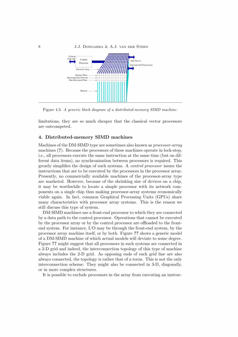

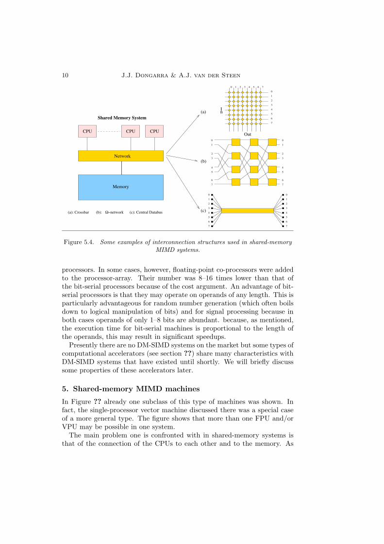


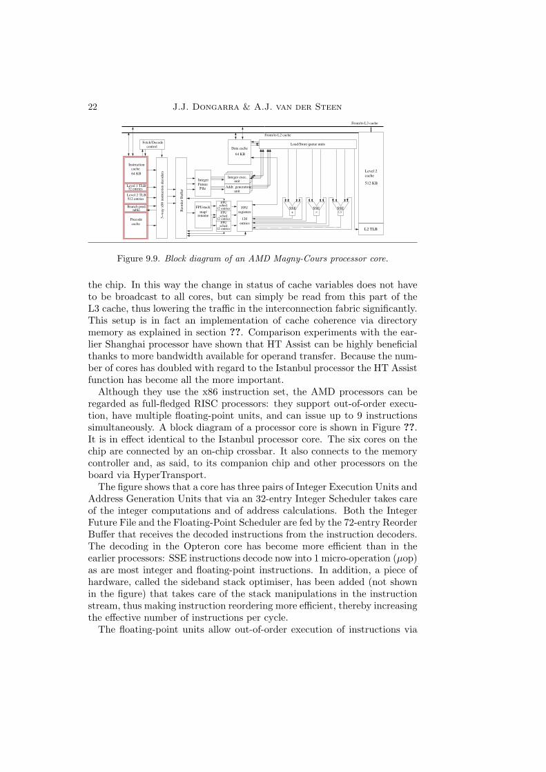

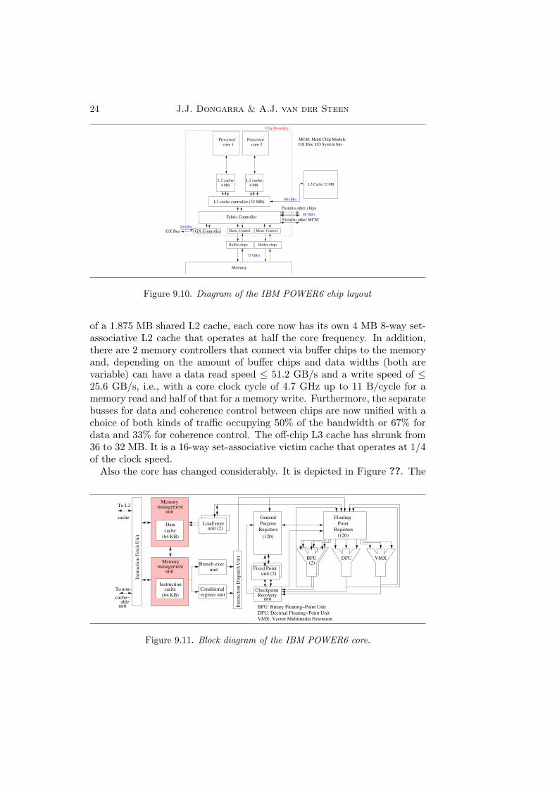


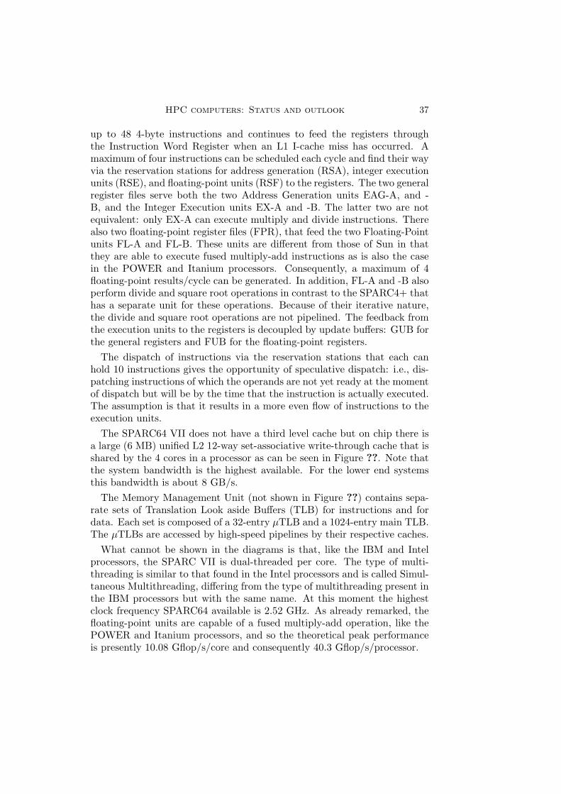
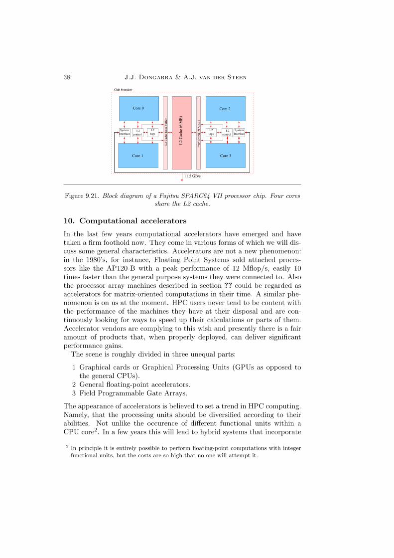


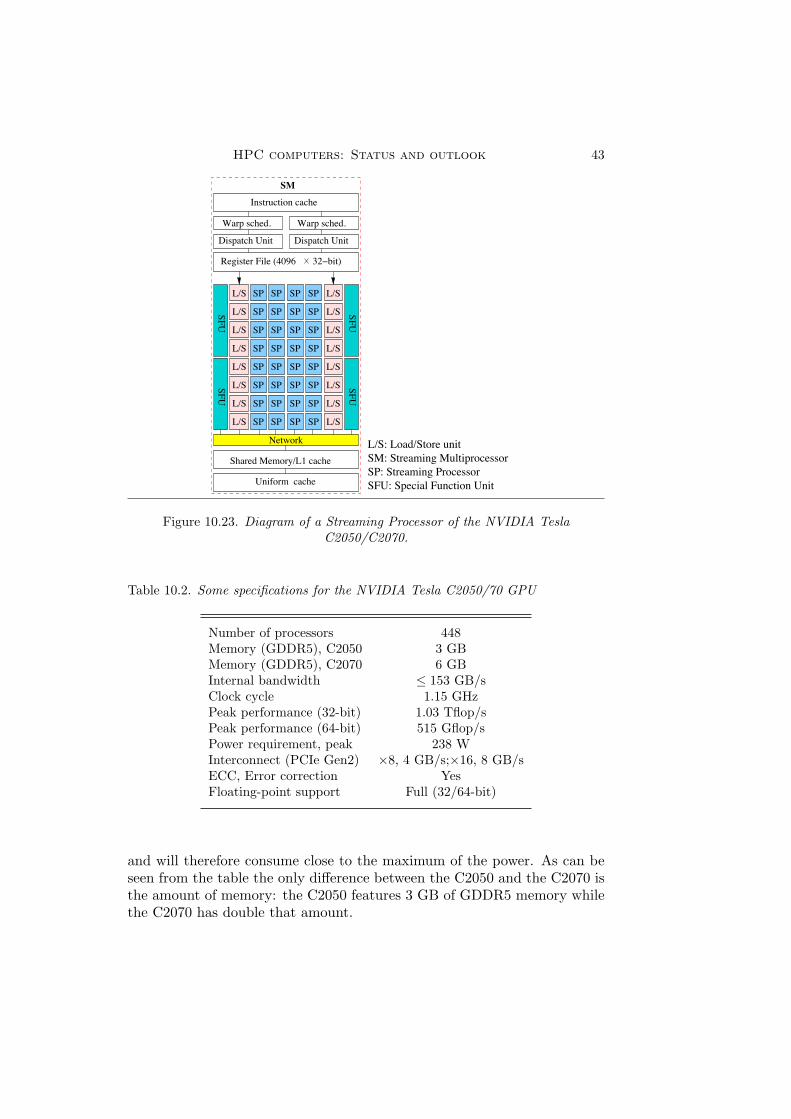


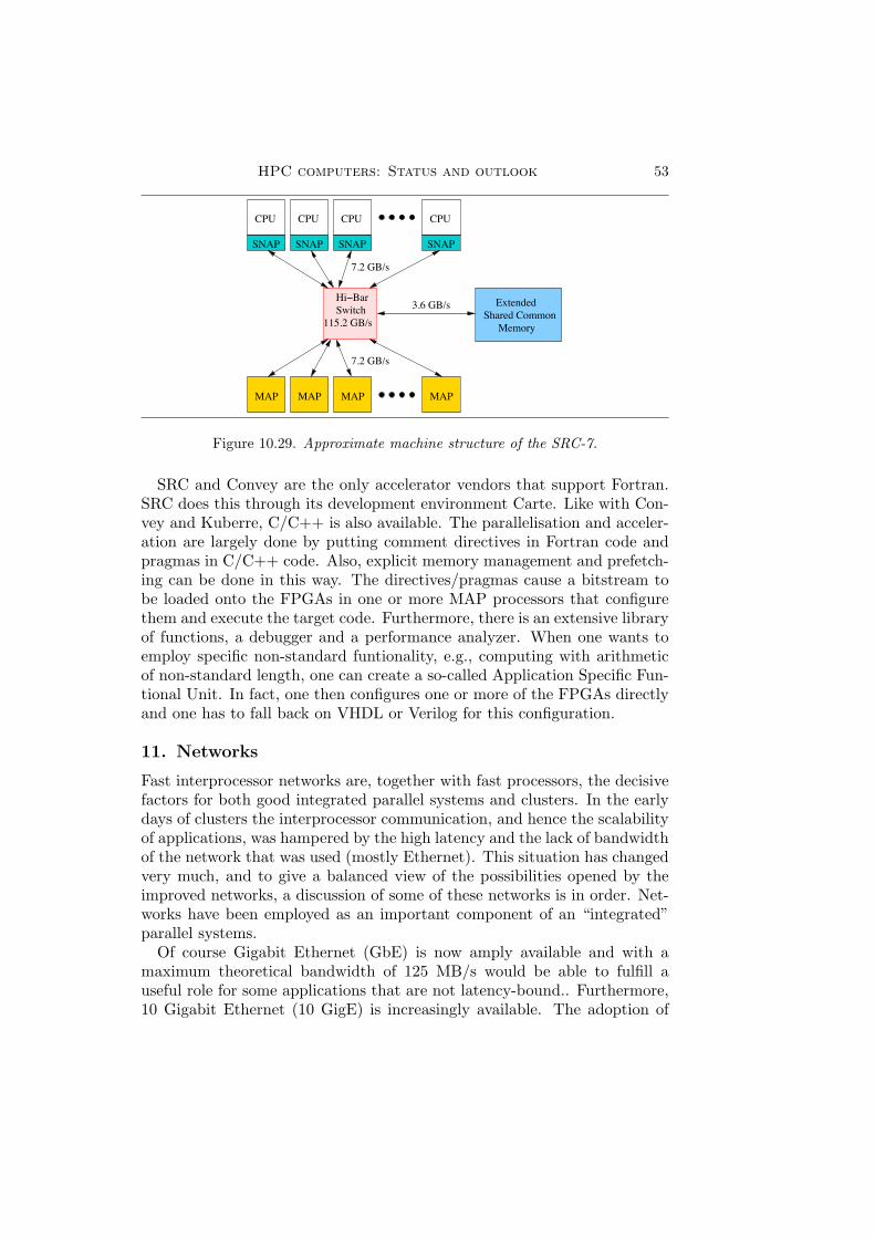


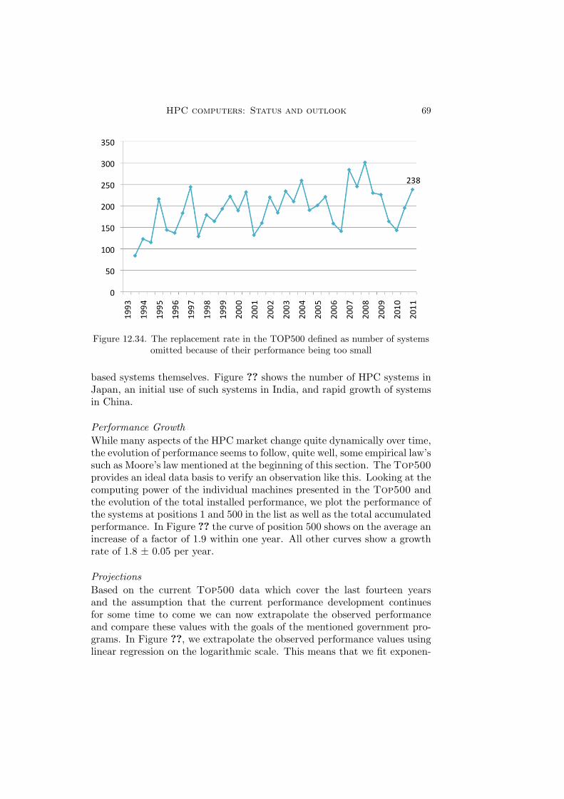
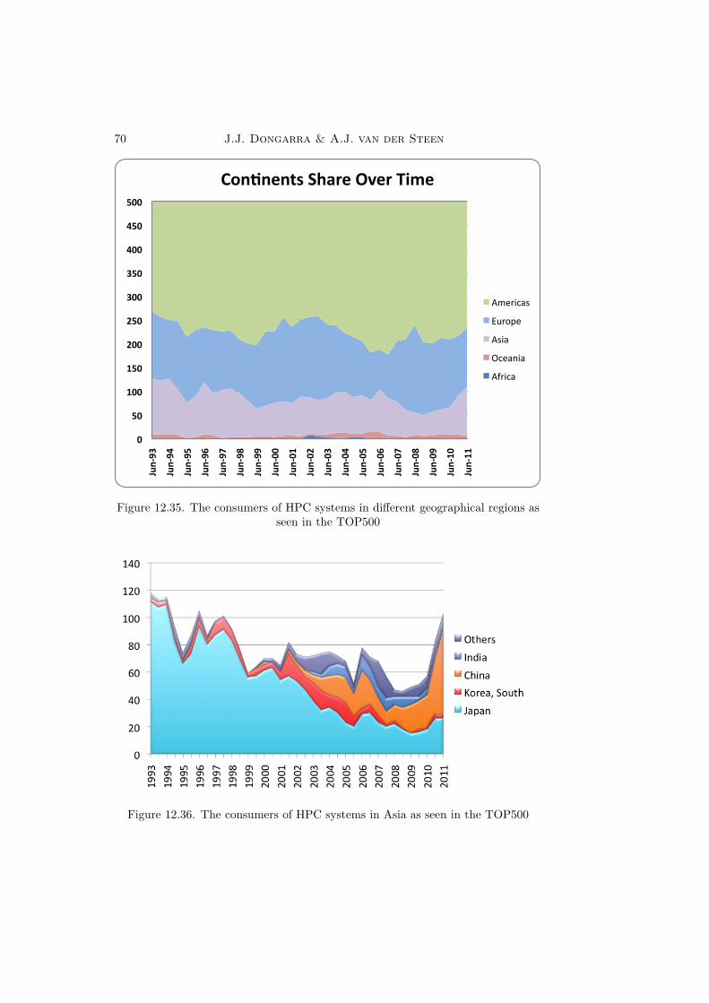


![Moore's Law - The Netlib · v e b een called the `sup ercomputers' of there time [4,2] w e indeed see ho ww ell this la w holds for almost the complete lifespan of mo dern computing.](https://static.documents.pub/doc/80x56/5fd8f72d608be5432003ed28/moores-law-the-v-e-b-een-called-the-sup-ercomputers-of-there-time-42-w-e.jpg)
![Self Adaptivity in Grid Computing - Netlib · v2.02] Self Adaptivity in Grid Computing Sathish S. Vadhiyar1, and Jack J. Dongarra2,3 1 Supercomputer Education and Research Centre](https://static.documents.pub/doc/80x56/5fa700c0531bda55915b73a0/self-adaptivity-in-grid-computing-v202-self-adaptivity-in-grid-computing-sathish.jpg)