32
High-Performance SRAM Design Rahul Rao IBM Systems and Technology Group

High-Performance SRAM Design
Rahul Rao
IBM Systems and Technology Group

Exercise
READ Path
WWL
WBL WBLb
RWL
RBL READ Path
WWL
WBL WBLb
RWL
RBL
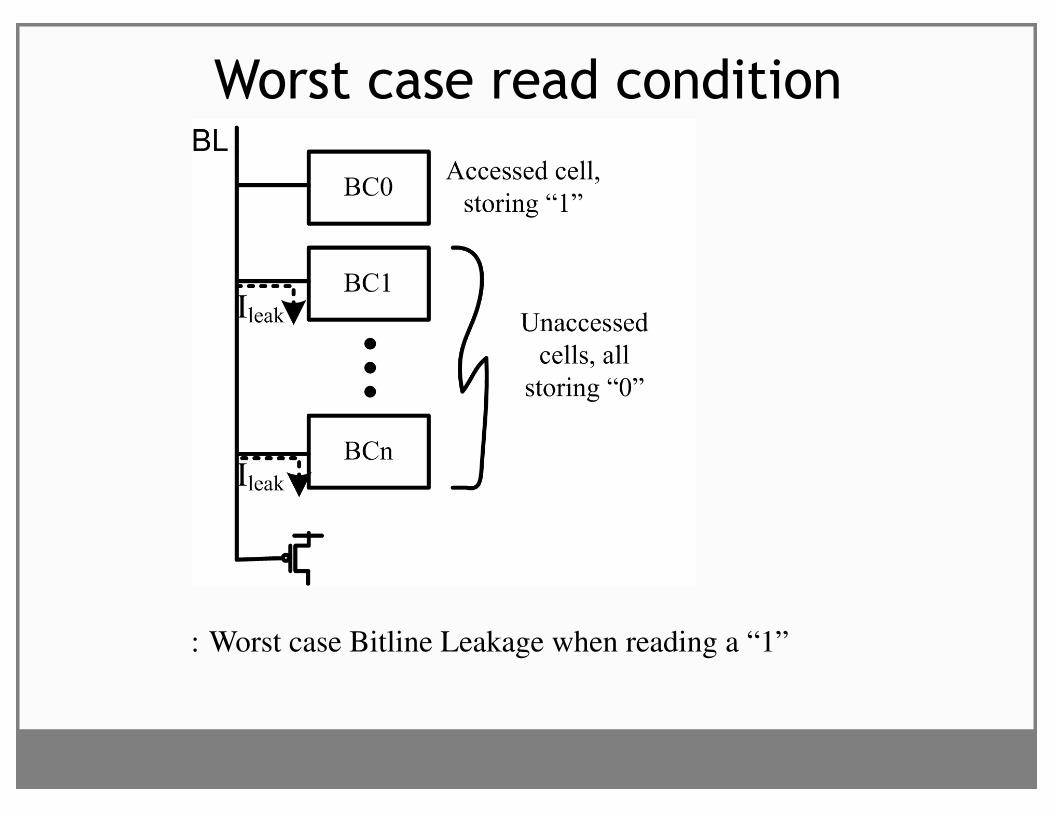
Worst case read conditionChapter 3. 5T Basics 17
Figure 3.6: Worst case Bitline Leakage when reading a “1”
This problem worsens in the presence of variations in BL leakage and in the threshold voltage
of the dynamic inverter’s PFET. Figure 3.7 shows the ideal scenario for the BL and V
T
variations
to not affect the read. As shown, ideally the variation in V
DD
�V
T P
lies in between the possible
variation of the BL voltage when either a “1” or “0” is being read. If the variation of the BL voltage
overlaps with the variation of V
DD
�V
T
, the need to design for the worst case will lead to increasing
device sizes to reduce variation. For example, V
T
variation can be reduced by widening up the PU
device in the dynamic inverter. This reduces the probability of overlap between the two variations.
However, this increases area and power dissipation.
Figure 3.7: BL voltage and V
T
variations: ideal scenario

Data Independent Leakage Cell25
M4
M3M1
M2
M6M5
WLVDD
M10
M7
M8M9
BL BLRdWL RdBL
VDD
Figure 9 (c): Schematic of Ten transistors with M9 and M10 added to schematic of eight transistor to lower leakage power
(Calhoun, 2010)
4
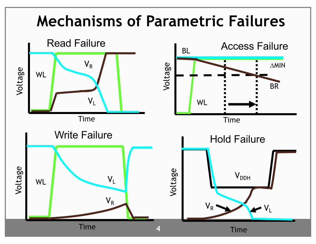
Mechanisms of Parametric Failures
WL
Volt
age
Time Time
Volt
age
VDDH
WLVR
VL
Volt
age
Time
Read Failure
VR
VL
Write Failure Hold Failure
VR VL
Time
DMIN
WL
BL
BR
Access Failure
Volt
age
q Which of the following are true for the 6-T SRAM cell
a) A cell with poor READ margin is unlikely to have access
failure
b) Differential read means there is no worst case data
condition for read
c) The worst case write condition is having cells with alternate
0s and 1 along the column
d) Access fails can be minimized by running the array at a
slower frequency
Question
Slide 5

q Introduction to memory
q SRAM basics and bitcell array (refresher)
q Current Challenges
q Alternative Cell Types (6 to 10T), Asymmetric Cells, Sub-
threshold Cells, Low – leakage cells
q Impact of Variation, Assist Circuits
q BTI and impact on SRAMs
q Power
Topics
Slide 6

7
Sources of Manufacturing Variations

8
Impact of Manufacturing Variations
Location of Identical Ring Oscillators on a Die
Frequency Correlation(averaged over 300 die)
Manjul Bhushan, ICMTS, 2005
9
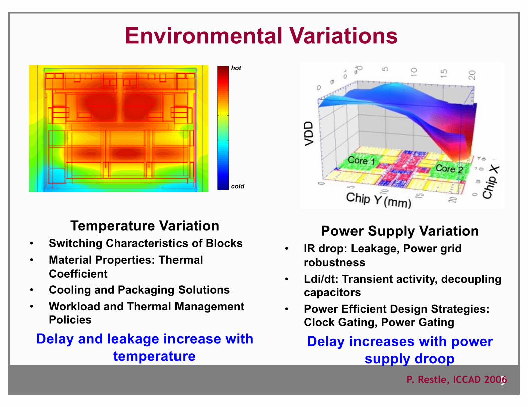
Environmental Variations
cold
hot
Temperature Variation• Switching Characteristics of Blocks• Material Properties: Thermal
Coefficient• Cooling and Packaging Solutions• Workload and Thermal Management
PoliciesDelay and leakage increase with
temperature
Power Supply Variation• IR drop: Leakage, Power grid
robustness• Ldi/dt: Transient activity, decoupling
capacitors• Power Efficient Design Strategies:
Clock Gating, Power GatingDelay increases with power
supply droopP. Restle, ICCAD 2006
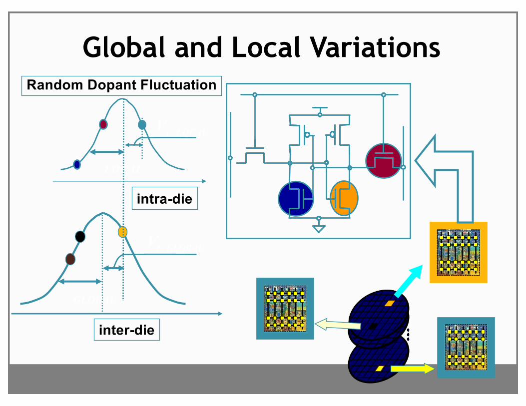
Global and Local Variations
inter-die
GLOBAL
t GLOBALV
intra-die
LOCAL
t LOCALV
Random Dopant Fluctuation

Hold Failure
AXR
BL BR
WL=0
L=‘1’
R=‘0’NR
PR
NL
PLAXL
VDDH
Time ->
WL VR
VLVo
ltage VDDH
Time ->
VR
VLWL
Volta
ge
VDDH
S. Mukhopadhyay, ITC 2010
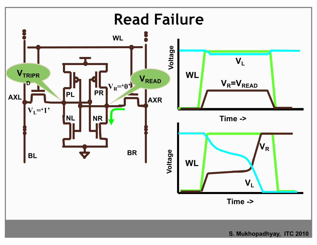
Read Failure
BL BR
WL
VL=‘1’
VR=‘0’VREAD
NR
PR
NL
PLAXRAXL
VTRIPRD VR=VREAD
VL
WL
Volta
ge
Time ->
WL
VR
VL
Volta
ge
Time ->
S. Mukhopadhyay, ITC 2010
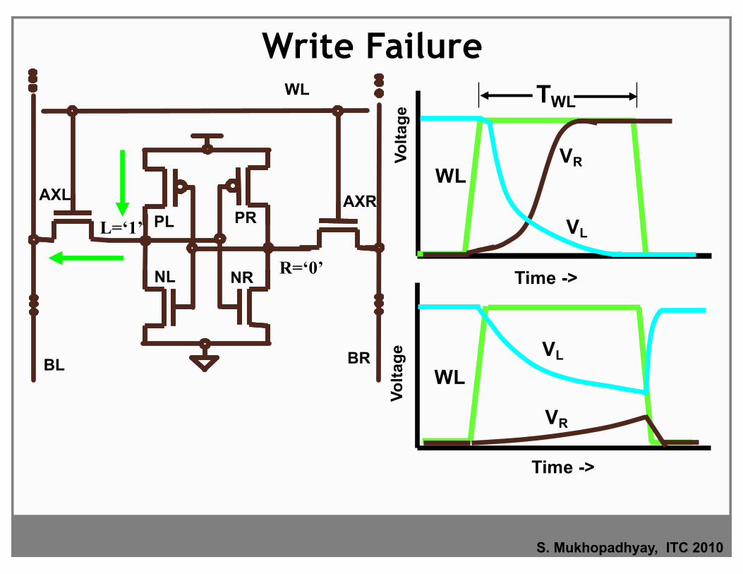
Write Failure
AXR
BL BR
WL
L=‘1’
R=‘0’NR
PR
NL
PLAXL
VR
VL
WL
Volta
ge
Time ->
WL
VR
VL
Volta
ge
Time ->
TWL
S. Mukhopadhyay, ITC 2010
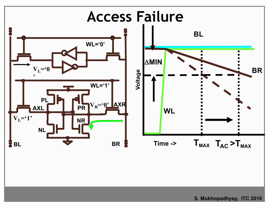
Access Failure
BL BR
WL=‘1’
VL=‘1’
VR=‘0’
NR
PR
NL
PLAXRAXL
VL=‘0’
WL=‘0’
TMAX
WL
BL
BRDMIN
TAC >TMAXVo
ltage
Time ->
S. Mukhopadhyay, ITC 2010
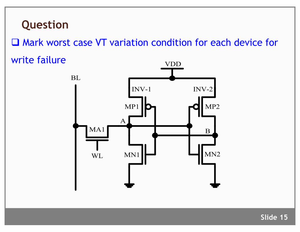
q Mark worst case VT variation condition for each device for
write failure
Question
Slide 15
2. Existing 6T and 5T SRAM Cell Topologies
The standard 6T SRAM is built up of two cross-coupled inverters (INV-1 and INV-2) and two access transistors (MA1 and MA2), connecting the cell to the bit lines (BL and BLB), as shown in Fig. 1 [7]. The pair of cross-coupled inverters is formed by a pair of load transistors (MP1 and MP2) and a pair of driver transistors (MN1 and MN2) that are stronger than the access transistors. More specifically, the cross-coupled inverters of the memory cell have two storage nodes A and B functioning to store either logic ‘1’ or logic ‘0’. The gates of access transistors are connected to a word line WL, and a rising transition on the word line to assert the access transistors during a read or a write operation. At the end of the read and write operations, the word line WL is de-asserted to allow the cross-coupled inverters to function normally and hold the logic state of the storage nodes. A concern associated with the read operation is that because of the back-to-back connection of cross-coupled inverters, a regenerative action develops and node A is pulled high resulting in the destruction of contents in the bit cell. Especially, when a logic ‘0’ stored initially, the voltage rise in the cell may corrupt the data stored. Therefore, it is desirable to keep the voltage at the storage node which has a logic ‘0’ stored from rising above the trip-voltage of the inverter. To provide a non-destructive read operation, the cell ratio (CR) was conventionally varied from 1 to 2.5 [2], where the W/L ratio of the driver transistor to the access transistor is referred to as the cell ratio. Similarly, for a successful write operation, both access transistors must be stronger than the load transistors. The ratio of the load transistor to the access transistor is referred to as the pull-up ratio (PR). To improve the read-ability of an SRAM cell, cell ratio can be increased, while a lower pull-up ratio is desirable to improve the cell write-ability. Figure 2 is a circuit diagram of a traditional 5T SRAM cell [8]. As shown in Fig. 2, the access transistor MA2 and bit line BLB in Fig. 1 have been removed to provide a five-transistor configuration. The removal of such access transistor allows for an area savings up to 20-30% compared to the standard 6T SRAM cell, while its power consumption is substantially reduced by one half [9]. Although the traditional 5T SRAM cells offer such significant reductions in power consumption, a serious drawback is presented in that it is difficult to write ‘1’ to the cells. In detail, when the bit line BL is set high and the word line WL is asserted, the transistors MA1 and MN1 fight one another. To guarantee a correct write operation will occur, it is important to note that the storage node A must be pulled up (or down) above (or below) the trip-voltage of INV-2 within the word line WL is logic high, otherwise a write failure will occur. In more detail, writing
a logic ‘1’ to a cell when initially a logic ‘0’ is stored, the low storage node A of the cell must be pulled up by the pre-charged bit line BL above the trip-voltage of INV-2. Undoubtedly, to properly write the wanted bit in the cell, it may be necessary that the access transistor should be very conductive to force the cross-coupled inverters to change its equilibrium condition. However, the access transistor should have a reduced conductivity for good stability in reading and standby operations. These two requirements impose contradicting requirements on cell transistor sizing.
MP1
MN2MN1
VDD
MP2
MA1
WL
BL
AB
MA2
BLB
INV-1 INV-2
Fig. 1. Circuit diagram of standard 6T SRAM cell.
MP1
MN2MN1
MP2
MA1
WL
AB
BL
VDD
INV-1 INV-2
Fig. 2 Circuit diagram of traditional 5T SRAM cell.
As mentioned above, it is difficult to write ‘1’ to a memory cell that is storing a ‘0’. In order to resolve the write ‘1’ issue of the traditional 5T SRAM cells, several techniques have been developed. Some of these techniques rely on boosted word line voltage [10-12], reducing the supply voltage VDD [8-9], [13-14], sizing cell transistors [15-17], reduced bit line voltage [18-19], and raising the source voltage VSS [20-22]. However, each of these techniques may cause a reduction in the drive current of the transistors and in the operating speed of the cell, or has increased memory cell area and a degradation in the manufacturing accuracy, or requires generation of a voltage above the operating voltage, or requires a more complicated circuit design and more complicated device process. Hence, there is a need for an effective technique to improve the write-ability of 5T SRAM cells which suffer from inability to write ‘1’.
IJCSI International Journal of Computer Science Issues, Volume 13, Issue 5, September 2016 ISSN (Print): 1694-0814 | ISSN (Online): 1694-0784 www.IJCSI.org https://doi.org/10.20943/01201605.2835 29
2016 International Journal of Computer Science Issues
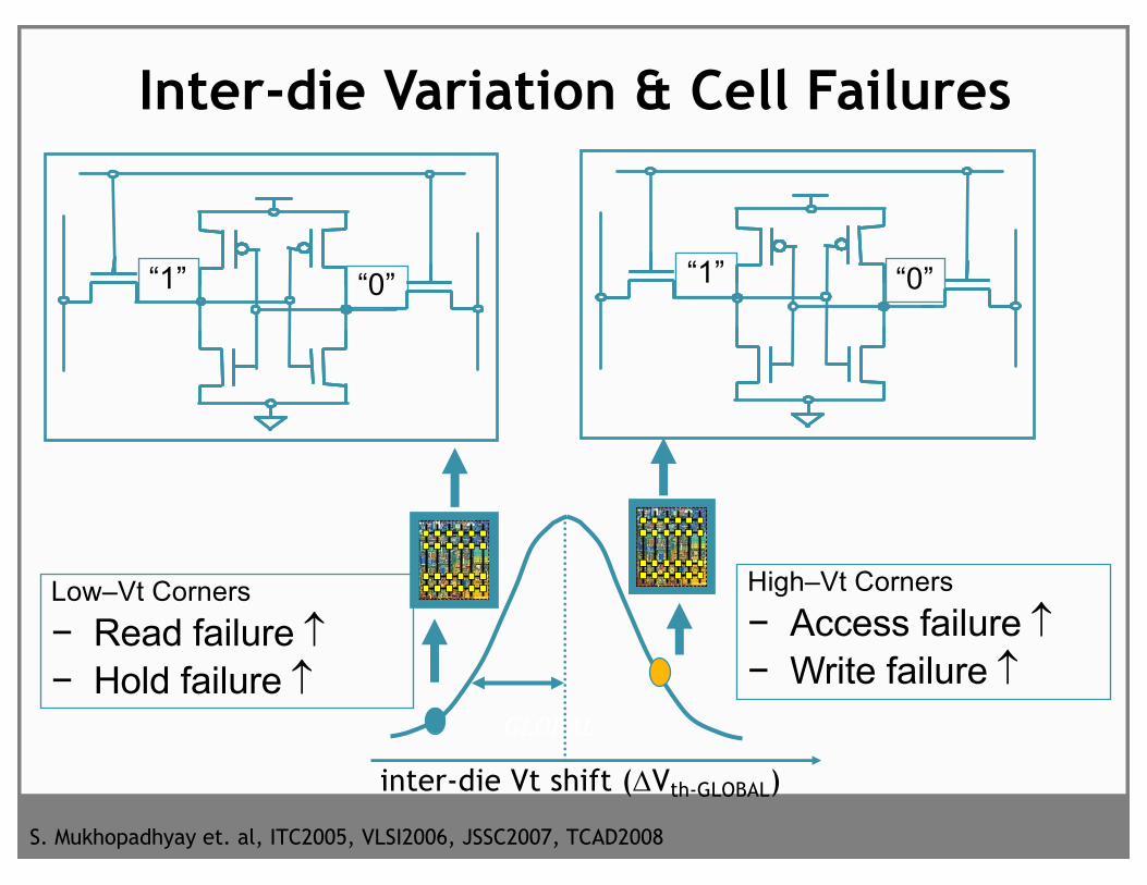
Inter-die Variation & Cell Failures
inter-die Vt shift (DVth-GLOBAL)
GLOBAL
“1” “0”
High–Vt Corners− Access failure − Write failure
“1” “0”
Low–Vt Corners− Read failure − Hold failure
S. Mukhopadhyay et. al, ITC2005, VLSI2006, JSSC2007, TCAD2008
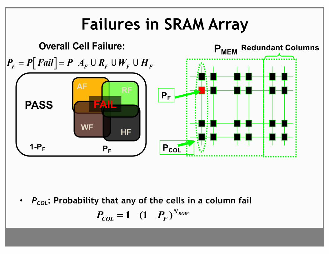
Failures in SRAM Array
• PCOL: Probability that any of the cells in a column fail
1 (1 ) ROWNCOL FP P=
PMEM
PF
PCOL
Redundant Columns
AF
WF
RF
HF
PASS FAIL
PF1-PF
[ ]F F F F FP P Fail P A R W H= = U U U
Overall Cell Failure:

Impact of Redundancy on Memory Failure
PMEM
Cell Failure
sVt
sVtFa
ilure
Pro
babi
lity
Redundant Col / Total Col. [%] Larger redundancy (1) more column to replace (less memory failure). (2) smaller cell area (larger cell failure).
Actual Col.Red. Col.
Total Area=Const.
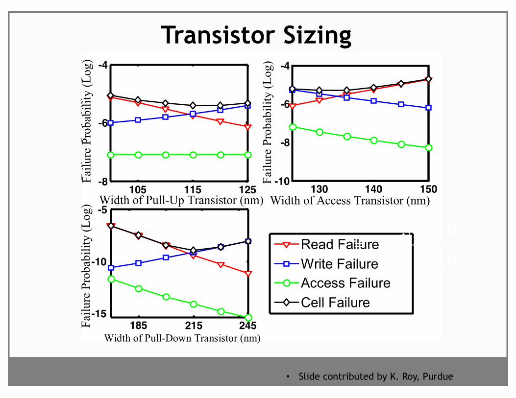
Transistor Sizing
Failu
re P
roba
bilit
y (L
og)
130 140 150 -10
-8
-6
-4
Width of Access Transistor (nm)
Read Failure Write Failure Access Failure Cell Failure
105 115 125 -8
-6
-4
Width of Pull-Up Transistor (nm)
185 215 245 -15
-10
-5
Width of Pull-Down Transistor (nm)
Failu
re P
roba
bilit
y (L
og)
Failu
re P
roba
bilit
y (L
og)
Failu
re P
roba
bilit
y (L
og)
• Slide contributed by K. Roy, Purdue
0i
MIN MINVt Vt
i i
L WLW
=

q Array redundancy
a) Improves cell stability
b) Degrades cell performance (i.e increases read and write
times)
c) Does not require any change to cell peripheral circuits
d) Row redundancy is better than column redundancy
Question
Slide 20
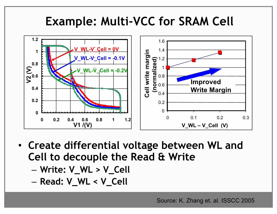
Example: Multi-VCC for SRAM Cell
• Create differential voltage between WL and Cell to decouple the Read & Write– Write: V_WL > V_Cell– Read: V_WL < V_Cell
0
0.2
0.4
0.6
0.8
1
1.2
0 0.2 0.4 0.6 0.8 1 1.2V1 /(V)
V2 (V
)
-V_WL-V_Cell = 0V-V_WL-V_Cell = -0.1V-V_WL-V_Cell = -0.2V
0
0.2
0.4
0.6
0.8
1
1.2
1.4
1.6
0 0.1 0.2 0.3
V_WL – V_Cell (V)
Cel
l writ
e m
argi
n (n
orm
aliz
ed)
Improved Write Margin
Source: K. Zhang et. al. ISSCC 2005
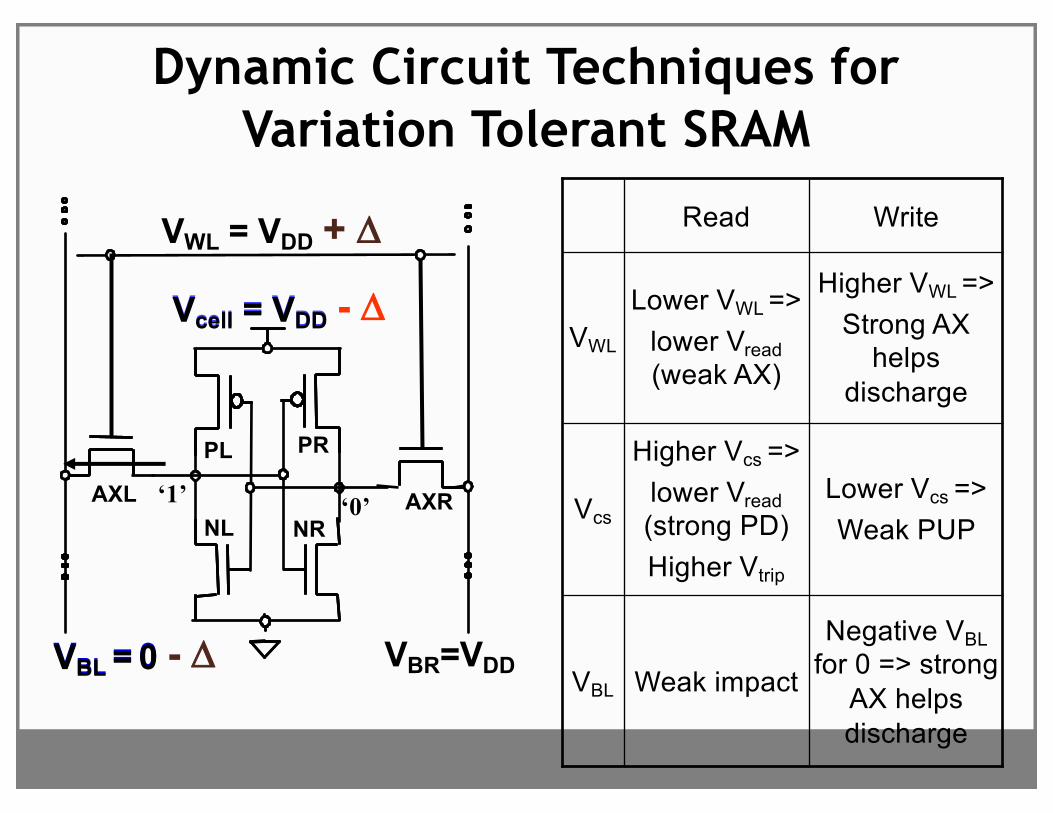
Dynamic Circuit Techniques for Variation Tolerant SRAM
VBL = 0 - D
VWL = VDD + D
‘1’ ‘0’NR
PR
NL
PL
AXRAXL
Vcell = VDD - D
VBR=VDDVBL = 0
Vcell = VDDHigher VWL =>
Strong AX helps
discharge
Lower VWL => lower Vread(weak AX)
VWL
Negative VBL for 0 => strong
AX helps discharge
Weak impactVBL
Lower Vcs => Weak PUP
Higher Vcs => lower Vread(strong PD) Higher Vtrip
Vcs
WriteRead
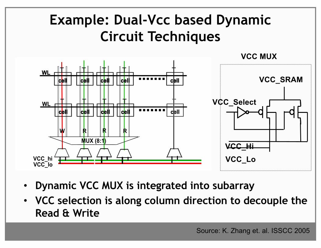
Example: Dual-Vcc based Dynamic Circuit Techniques
• Dynamic VCC MUX is integrated into subarray• VCC selection is along column direction to decouple the
Read & Write
VCC_HiVCC_Lo
VCC_Select
VCC_SRAM
VCC MUX
VCC_lo
cell cell cell cell cellWL
cell cell cell cell cellWL
MUX (8:1)W R R R
cellcell cellcell cellcell cellcell cellcellWL
cellcell cellcell cellcell cellcell
VCC_hiMUX MUX MUX MUX MUX
BI MUX
VCC MUX
VCC_lo
cellcell cellcell cellcell cellcell cellcellWL
cellcell cellcell cellcell cellcell cellcellWL
MUX (8:1)W R R R
cellcell cellcell cellcell cellcell cellcellWL
cellcell cellcell cellcell cellcell
VCC_hiMUX MUXMUX MUXMUX MUXMUX MUXMUX
BI MUX
VCC MUX
Source: K. Zhang et. al. ISSCC 2005
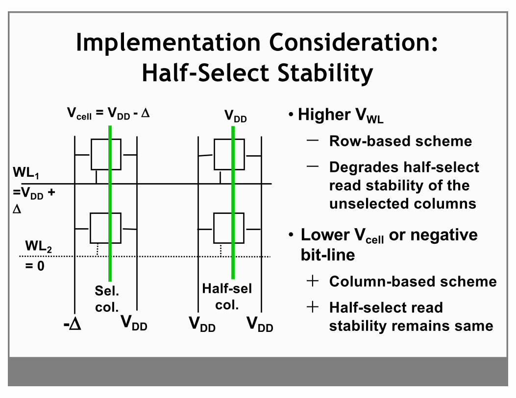
Implementation Consideration: Half-Select Stability
WL2
= 0
Vcell = VDD - D VDD
Sel. col.
Half-sel col.
WL1
=VDD + D
-D VDD VDD VDD
• Higher VWL
- Row-based scheme - Degrades half-select
read stability of the unselected columns
• Lower Vcell or negative bit-line+ Column-based scheme+ Half-select read
stability remains same

Negative Bit Line Scheme
Source: S. Mukhopadhyay, R. Rao et. al, TVLSI 2009
> REPLACE THIS LINE WITH YOUR PAPER IDENTIFICATION NUMBER (DOUBLE-CLICK HERE TO EDIT) <
3
C. Effect on Data-Retention Although a column-based scheme eliminates the degradation
in the half-select Read disturb failures, it can degrade the data
retention ability of the unselected cells in the selected column
(i.e. the data stored in the unselected cells can flip, resulting in a
data retention failure). For dynamic supply control, the data
retention failure probability can increase due to lower supply
voltage of the unselected cells. On the other hand, data
retention failures can occur in the negative bit-line scheme due
to increased leakage through the access transistor (Vgs = ∆BL >
0) in the unselected cells in the selected column.
We have estimated the data retention failure probability
considering similar reduction in the cell supply and (DC
negative) bit-line voltages. Fig. 3(a) plots the data retention
failure probability considering similar reduction in the cell
supply and bit-line voltage. The failure probability increases at
a greater rate for the DC negative bit-line scenario, as compared
to the reduced supply voltage scenario. This places a constraint
on the maximum DC negative bit-line voltage that can be used
to enhance the write-ability of the cell.
This was further verified by measuring the static noise
margin for an array of 120 cells. The cells were manufactured
in a 45nm SOI technology, and the mean hold noise margin for
various reductions in cell and bit-line voltages is plotted in Fig.
3(b). As expected, a similar trend can be observed, with the
hold noise margin decreasing rapidly with DC negative bit-line
voltages. In fact, it reduces to 0 at a negative bit line voltage of
200mV, indicating a data retention failure in all cells.
III. TRANSIENT NEGATIVE BIT-LINE TECHNIQUE A DC negative bit-line voltage level requires a negative
voltage source (on-chip or off-chip) and level converters at the
drivers. Both these requirements increase the design
complexity. On-chip generation of a DC negative bias requires
a charge-pump which increases the power dissipation. In
addition, the application of a static negative bias is likely to
result in reliability concerns due to the increased electric field
across the devices. The DC negative bit line voltage also
degrades the hold stability as shown in the section II. C. To
eliminate these issues while preserving the benefit of the
negative bit-line voltage, we propose a capacitive coupling
based technique (Tran-NBL) for generating a transient negative
pulse on the appropriate bit-line.
A. Basic Concept A Write operation is essentially composed of two parts:
(a) Node storing ‘1’ (i.e. L in Fig. 1) is discharged till the
node voltage becomes equal to the voltage at the node storing
‘0’ (i.e. R in Fig. 1); and
(b) After voltage at the node L becomes lower than that at the
node R, the cross-coupled inverters ensures that node L reaches ‘0’ and node R reaches ‘1’ (Fig. 1).
The discharging time of part (a) is denoted as T1 and the
cross-coupled inverter action time in part (b) is T2. Normally T2
is much smaller than T1. The majority of the Write failures are
due to the effect of variations on T1. Variations delay the
discharge of the node L and T1 becomes larger than the
word-line turn-on time (TWL). If the node L is pulled down
below node R within the word-line turn-on time, the
cross-coupled inverter action will most likely ensure the write
operations.
1.0E+00
1.0E+02
1.0E+04
1.0E+06
1.0E+08
1.0E+10
0 0.05 0.1 0.15 0.2
Change in bit line or cell supply voltage [V]
Failu
re P
roba
bilit
y (S
imul
atio
n)
DC Negative Bit Line
Reduced Supply Voltage
(a) Reduction in Data Retention Failure Probability (Monte Carlo Simulation [7])
0.0
0.2
0.4
0.6
0.8
1.0
0 0.05 0.1 0.15 0.2
Change in bit line or cell supply voltage [V]
Hol
d N
oise
Mar
gin
(Mea
sure
d)
DC Negative Bit Line
Reduced Supply Voltage
(b) Reduction in Hold Noise Margin (Measured) Fig. 3: Date-retention failures and noise margin for voltage
changes at cell terminals
CBL
VBLVinCboost
cell
DB=“1”
BIT_EN
D=“0”
BL BR
Cboost
NSEL
BIT_EN generating
block
WR
CS
PCHG
NBL,PBL NBR,PBR
P1 P2
NSEL
Conventional
WL,PCHG
BL BRBIT_EN
&NSEL
∆ ~ Cboost/CBL
WL,PCHG
BL BR
This SchemeConventional
WL,PCHG
BL BRBIT_EN
&NSEL
∆ ~ Cboost/CBL
WL,PCHG
BL BR
This Scheme
CBL
VBLVinCboost
CBLCBLCBL
VBLVinCboost
cell
DB=“1”
BIT_EN
D=“0”
BL BR
Cboost
NSELNSEL
BIT_EN generating
block
WR
CS
PCHG
NBL,PBL NBR,PBR
P1 P2
NSEL
Conventional
WL,PCHG
BL BRBIT_EN
&NSEL
∆ ~ Cboost/CBL
WL,PCHG
BL BR
This SchemeConventional
WL,PCHG
BL BRBIT_EN
&NSEL
∆ ~ Cboost/CBL
WL,PCHG
BL BR
This Scheme
Fig. 4. The proposed Tran-NBL scheme.

Effectiveness Considerations: Writability improvement
• Various dynamic schemes have different effectiveness in improving writability for similar read stability
– Higher VWL is most effective
100
10-5
10-10
10-15
Nor
m. w
rite
fail
prob
0 50 100 150 200change in terminal voltage (D) [mV]
VWL = VDD + D
VBL = - D
Vcell = VDD - D
Fast Monte-Carlo simulations for 45nm PD/SOI
VBL = - D
Vcell = VDD - D
Source: S. Mukhopadhyay, R. Rao et. al, TVLSI 2009

Impact on Active Data-Retention
• Column based read-write control adversely impact the active data-retention failures
– DC negative bitline has higher active data-retention failures– Tran-NBL and lower Vcs have comparable failure rates
WL2
= 0
Vcell = VDD - D
Sel. col.-D VDD
Active data-retention fails
Fail probabilities are normalized to write fail prob. at nominal condition
DC-NBL
Lower Vcell
Source: S. Mukhopadhyay, R. Rao et. al, TVLSI 2009

Assist Methods
q Of the various assist methods
a) Negative bit line scheme does not help 8-T sram cell
b) Word line under drive does not help 8-T sram cell
c) Word line over drive does not help 7-T conditionally
decoupled sram cell
d) VCDL does not help any kind of assymetric sram cell
Question
Slide 30
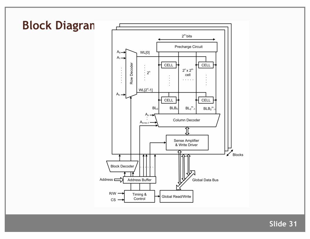
Block Diagram
Slide 31
13
Figure 2.1 SRAM architecture
CELL
WL[0]
WL[2n-1]
BL0
Row
Dec
oder
A0
A1
An
2n 2n x 2m
cell
CELL
CELL
CELL
Column Decoder
Precharge Circuit
BLB2m
-1BL2m
-1BLB0
An
An+m-1
Sense Amplifier & Write Driver
Timing & ControlCS
R/WGlobal Read/Write
Global Data Bus
2m bits
Address BufferAddress
Blocks
Block Decoder
signals is used for the determination of read or write operation and the chip set (CS)
signal is usually employed in multi-chip designs.
During the read operation the integrated SA on each column (sometimes shared
between more columns) will be employed to read the data. In write operation, the write
drivers will force the BL and BLB of selected column to ‘0’ or ‘1’ and the input data will
be written into the internal nodes of the selected cell.
Hence, a typical column of SRAM consists of the following blocks:


