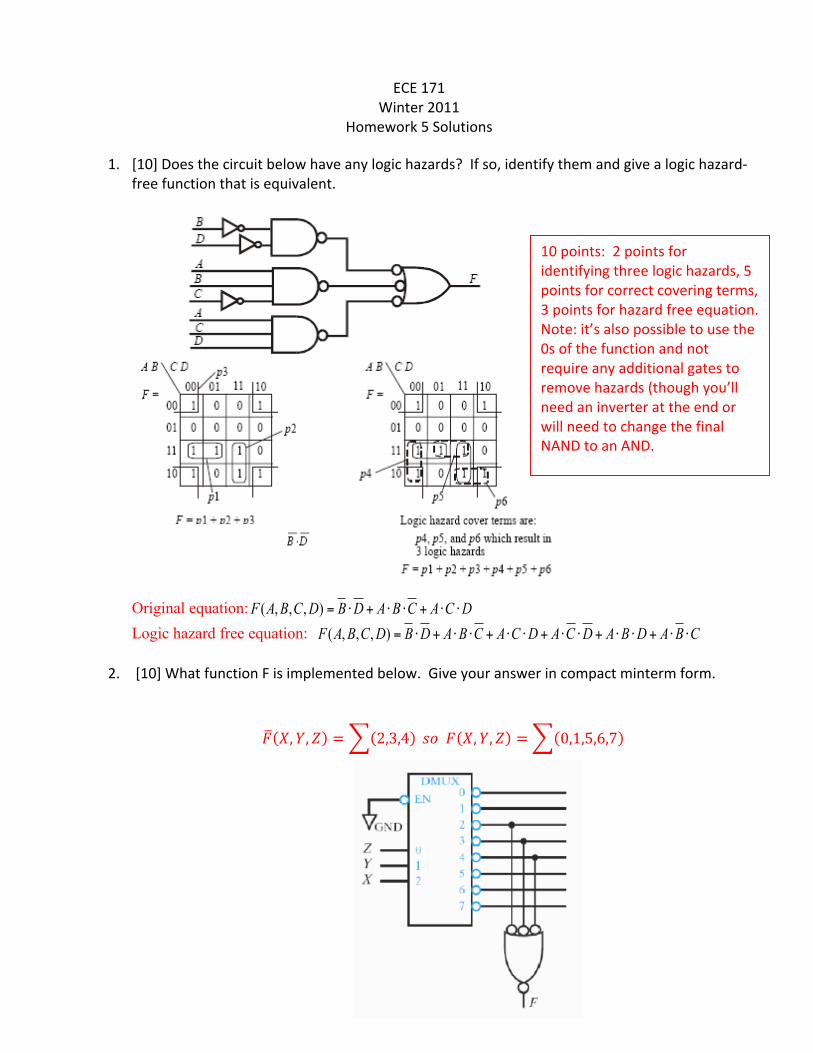
ECE 171 Winter 2011 Homework 5 Solutions 1. [10] Does the circuit below have any logic hazards? If so, identify them and give a logic hazard free function that is equivalent. Original equation: ( , , , ) FABCD BD ABC ACD = ⋅ + ⋅ ⋅ + ⋅ ⋅ Logic hazard free equation: ( , , , ) FABCD BD ABC ACD ACD ABD ABC = ⋅ + ⋅ ⋅ + ⋅ ⋅ + ⋅ ⋅ + ⋅ ⋅ + ⋅ ⋅ 2. [10] What function F is implemented below. Give your answer in compact minterm form. ! !, !, ! = 2,3,4 !" ! !, !, ! = 0,1,5,6,7 10 points: 2 points for identifying three logic hazards, 5 points for correct covering terms, 3 points for hazard free equation. Note: it’s also possible to use the 0s of the function and not require any additional gates to remove hazards (though you’ll need an inverter at the end or will need to change the final NAND to an AND.
Transcript
ECE 171 Winter 2011
Homework 5 Solutions
1. [10] Does the circuit below have any logic hazards? If so, identify them and give a logic hazard-‐free function that is equivalent.
Original equation: ( , , , )F A B C D B D A B C A C D= ⋅ + ⋅ ⋅ + ⋅ ⋅ Logic hazard free equation: ( , , , )F A B C D B D A B C A C D A C D A B D A B C= ⋅ + ⋅ ⋅ + ⋅ ⋅ + ⋅ ⋅ + ⋅ ⋅ + ⋅ ⋅
2. [10] What function F is implemented below. Give your answer in compact minterm form.
! !,!,! = 2,3,4 !" ! !,!,! = 0,1,5,6,7
10 points: 2 points for identifying three logic hazards, 5 points for correct covering terms, 3 points for hazard free equation. Note: it’s also possible to use the 0s of the function and not require any additional gates to remove hazards (though you’ll need an inverter at the end or will need to change the final NAND to an AND.
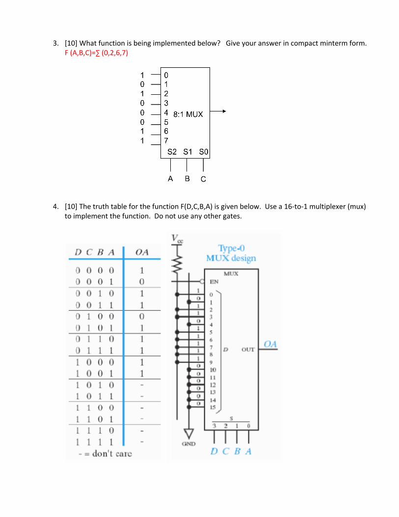
3. [10] What function is being implemented below? Give your answer in compact minterm form. F (A,B,C)=∑ (0,2,6,7)
4. [10] The truth table for the function F(D,C,B,A) is given below. Use a 16-‐to-‐1 multiplexer (mux) to implement the function. Do not use any other gates.
5. [10] Implement the same function from problem 4 using an 8-‐to-‐1 mux. You may also use an
inverter.
6. [10] What function is being implemented by the circuit below? Give your answer in compact
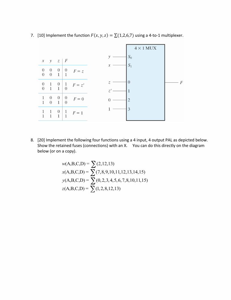
7. [10] Implement the function ! !,!, ! = (1,2,6,7) using a 4-‐to-‐1 multiplexer.
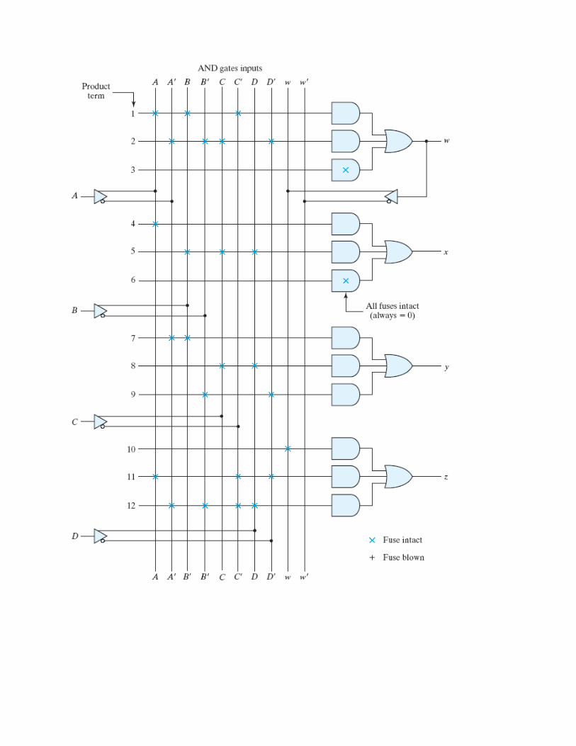
8. [20] Implement the following four functions using a 4 input, 4 output PAL as depicted below. Show the retained fuses (connections) with an X. You can do this directly on the diagram below (or on a copy).
(A,B,C,D) = (2,12,13)
(A,B,C,D) = (7,8,9,10,11,12,13,14,15)
(A,B,C,D) = (0,2,3,4,5,6,7,8,10,11,15)
(A,B,C,D) = (1,2,8,12,13)
w
x
y
z
∑∑∑∑
Simplifying with K-‐maps, we obtain the following minimal equations:
(A,B,C,D) = (2,12,13)
A B C + A B C D(A,B,C,D) = (7,8,9,10,11,12,13,14,15)
A + B C D(A,B,C,D) = (0,2,3,4,5,6,7,8,10,11,15)
A B + C D + B D(A,B,C,D) = (1,2,8,12,13)
A B C + A B C D + A C D + A
w
x
y
z
= ⋅ ⋅ ⋅ ⋅ ⋅
= ⋅ ⋅
= ⋅ ⋅ ⋅
= ⋅ ⋅ ⋅ ⋅ ⋅ ⋅ ⋅ ⋅
∑
∑
∑
∑B C D
= + A C D + A B C Dw
⋅ ⋅
⋅ ⋅ ⋅ ⋅ ⋅
20 points: 5 for correct equation and PAL layout for each function w,x,y,z . Must either put X inside unused gate or on all inputs of the unused gates.
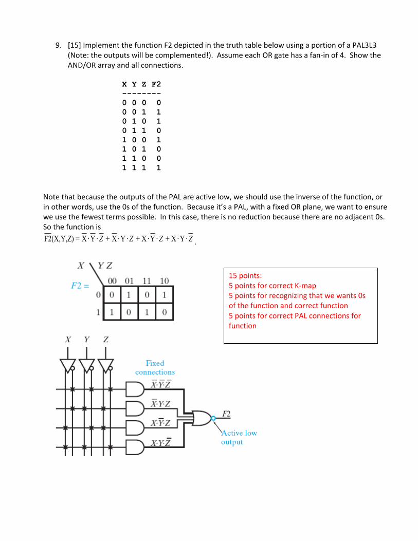
9. [15] Implement the function F2 depicted in the truth table below using a portion of a PAL3L3 (Note: the outputs will be complemented!). Assume each OR gate has a fan-‐in of 4. Show the AND/OR array and all connections.
Note that because the outputs of the PAL are active low, we should use the inverse of the function, or in other words, use the 0s of the function. Because it’s a PAL, with a fixed OR plane, we want to ensure we use the fewest terms possible. In this case, there is no reduction because there are no adjacent 0s. So the function is F2(X,Y,Z) = X Y + X Y + X Y + X YZ Z Z Z⋅ ⋅ ⋅ ⋅ ⋅ ⋅ ⋅ ⋅ .
15 points: 5 points for correct K-‐map 5 points for recognizing that we wants 0s of the function and correct function 5 points for correct PAL connections for function
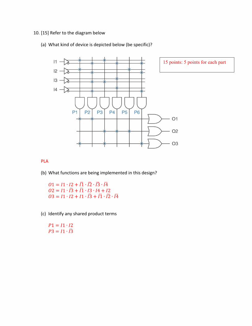
10. [15] Refer to the diagram below
(a) What kind of device is depicted below (be specific)?
PLA
(b) What functions are being implemented in this design?