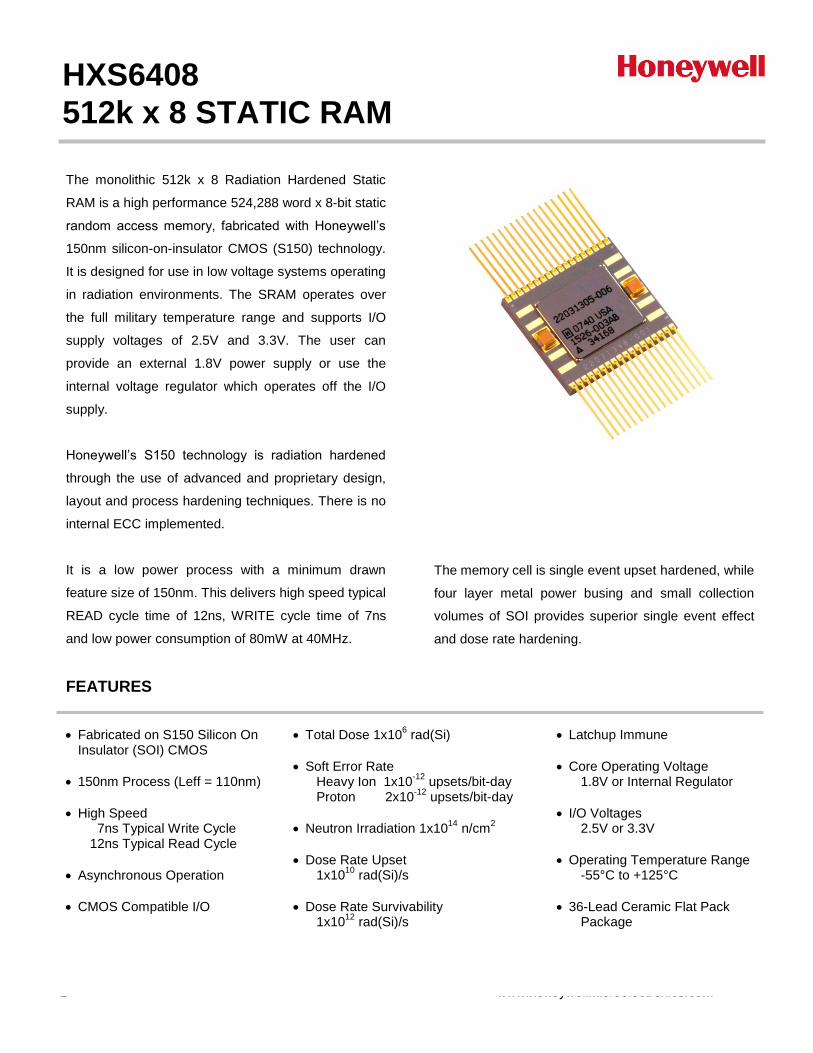
The monolithic 512k x 8 Radiation Hardened Static RAM is a high performance 524,288 word x 8-bit static random access memory, fabricated with Honeywell’s 150nm silicon-on-insulator CMOS (S150) technology. It is designed for use in low voltage systems operating in radiation environments. The SRAM operates over the full military temperature range and supports I/O supply voltages of 2.5V and 3.3V. The user can provide an external 1.8V power supply or use the internal voltage regulator which operates off the I/O supply. Honeywell’s S150 technology is radiation hardened through the use of advanced and proprietary design, layout and process hardening techniques. There is no internal ECC implemented. It is a low power process with a minimum drawn feature size of 150nm. This delivers high speed typical READ cycle time of 12ns, WRITE cycle time of 7ns and low power consumption of 80mW at 40MHz. The memory cell is single event upset hardened, while four layer metal power busing and small collection volumes of SOI provides superior single event effect and dose rate hardening. FEATURES Fabricated on S150 Silicon On Insulator (SOI) CMOS 150nm Process (Leff = 110nm) High Speed 7ns Typical Write Cycle 12ns Typical Read Cycle Asynchronous Operation CMOS Compatible I/O Total Dose 1x10 6 rad(Si) Soft Error Rate Heavy Ion 1x10 -12 upsets/bit-day Proton 2x10 -12 upsets/bit-day Neutron Irradiation 1x10 14 n/cm 2 Dose Rate Upset 1x10 10 rad(Si)/s Dose Rate Survivability 1x10 12 rad(Si)/s Latchup Immune Core Operating Voltage 1.8V or Internal Regulator I/O Voltages 2.5V or 3.3V Operating Temperature Range -55°C to +125°C 36-Lead Ceramic Flat Pack Package HXS6408 512k x 8 STATIC RAM
Transcript
HXS6408
1 www.honeywellmicroelectronics.com
The monolithic 512k x 8 Radiation Hardened Static
RAM is a high performance 524,288 word x 8-bit static
It is designed for use in low voltage systems operating
in radiation environments. The SRAM operates over
the full military temperature range and supports I/O
supply voltages of 2.5V and 3.3V. The user can
provide an external 1.8V power supply or use the
internal voltage regulator which operates off the I/O
supply.
Honeywell’s S150 technology is radiation hardened
through the use of advanced and proprietary design,
layout and process hardening techniques. There is no
internal ECC implemented.
It is a low power process with a minimum drawn
feature size of 150nm. This delivers high speed typical
READ cycle time of 12ns, WRITE cycle time of 7ns
and low power consumption of 80mW at 40MHz.
The memory cell is single event upset hardened, while
four layer metal power busing and small collection
volumes of SOI provides superior single event effect
and dose rate hardening.
FEATURES
Fabricated on S150 Silicon On Insulator (SOI) CMOS
150nm Process (Leff = 110nm)
High Speed 7ns Typical Write Cycle 12ns Typical Read Cycle
Asynchronous Operation
CMOS Compatible I/O
Total Dose 1x10⁶ rad(Si)
Soft Error Rate Heavy Ion 1x10
-12 upsets/bit-day
Proton 2x10-12
upsets/bit-day
Neutron Irradiation 1x10¹⁴
n/cm2
Dose Rate Upset 1x10
10 rad(Si)/s
Dose Rate Survivability 1x10
12 rad(Si)/s
Latchup Immune
Core Operating Voltage 1.8V or Internal Regulator
I/O Voltages 2.5V or 3.3V
Operating Temperature Range -55°C to +125°C
36-Lead Ceramic Flat Pack Package
HXS6408
512k x 8 STATIC RAM
HXS6408
2 www.honeywellmicroelectronics.com
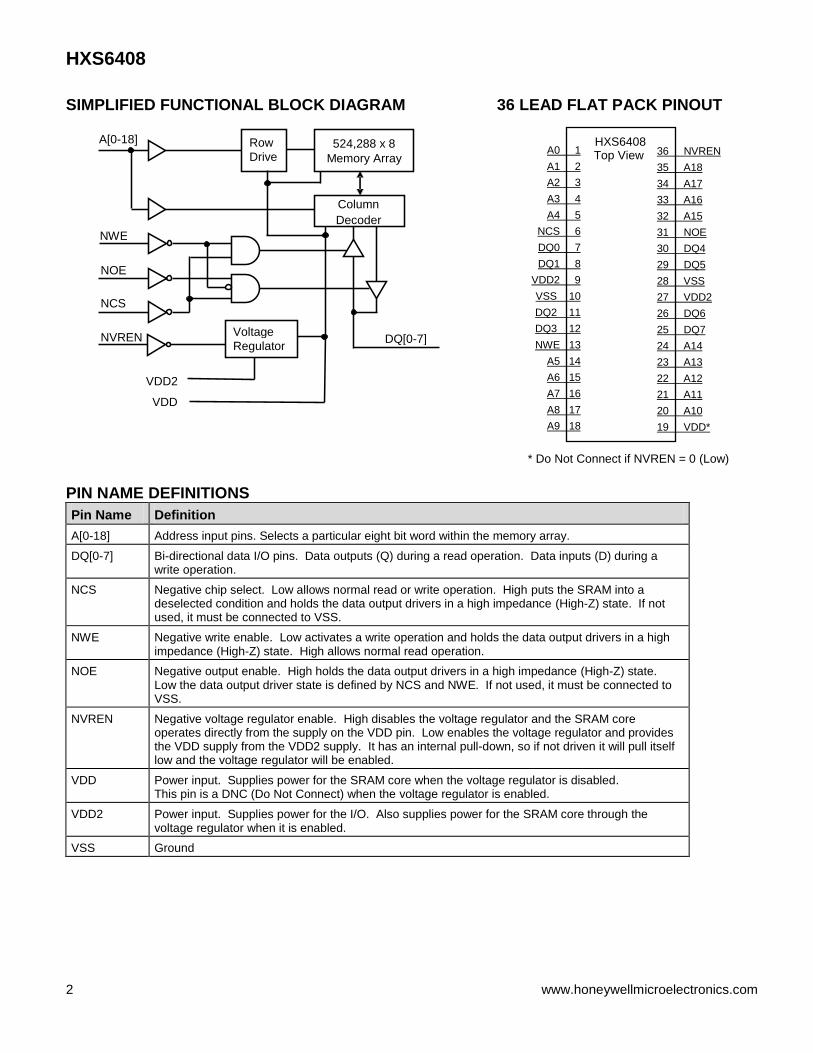
SIMPLIFIED FUNCTIONAL BLOCK DIAGRAM 36 LEAD FLAT PACK PINOUT
PIN NAME DEFINITIONS
Pin Name Definition
A[0-18] Address input pins. Selects a particular eight bit word within the memory array.
DQ[0-7] Bi-directional data I/O pins. Data outputs (Q) during a read operation. Data inputs (D) during a write operation.
NCS Negative chip select. Low allows normal read or write operation. High puts the SRAM into a deselected condition and holds the data output drivers in a high impedance (High-Z) state. If not used, it must be connected to VSS.
NWE Negative write enable. Low activates a write operation and holds the data output drivers in a high impedance (High-Z) state. High allows normal read operation.
NOE Negative output enable. High holds the data output drivers in a high impedance (High-Z) state. Low the data output driver state is defined by NCS and NWE. If not used, it must be connected to VSS.
NVREN Negative voltage regulator enable. High disables the voltage regulator and the SRAM core operates directly from the supply on the VDD pin. Low enables the voltage regulator and provides the VDD supply from the VDD2 supply. It has an internal pull-down, so if not driven it will pull itself low and the voltage regulator will be enabled.
VDD Power input. Supplies power for the SRAM core when the voltage regulator is disabled. This pin is a DNC (Do Not Connect) when the voltage regulator is enabled.
VDD2 Power input. Supplies power for the I/O. Also supplies power for the SRAM core through the voltage regulator when it is enabled.
VSS Ground
524,288 x 8 Memory Array
Column
Decoder
Row Drive
A[0-18]
DQ[0-7]
NWE
NOE
NCS
Voltage Regulator
VDD
VDD2
NVREN
A0 1
A1 2
A2 3
A3 4
A4 5
NCS 6
DQ0 7
DQ1 8
VDD2 9
VSS 10
DQ2 11
DQ3 12
NWE 13
A5 14
A6 15
A7 16
A8 17
A9 18
36 NVREN
35 A18
34 A17
33 A16
32 A15
31 NOE
30 DQ4
29 DQ5
28 VSS
27 VDD2
26 DQ6
25 DQ7
24 A14
23 A13
22 A12
21 A11
20 A10
19 VDD*
HXS6408 Top View
* Do Not Connect if NVREN = 0 (Low)
HXS6408
www.honeywellmicroelectronics.com 3
TRUTH TABLE
NCS NVREN NWE NOE VOLTAGE REGULATOR MODE DQ MODE
L L H L Enabled Read Data Out
L L L X Enabled Write Data In
L L H H Enabled Read Standby High-Z
X L X H Enabled Output Disabled High-Z
H L X X Enabled Deselected High-Z
L H H L Disabled Read Data Out
L H L X Disabled Write Data In
L H H H Disabled Read Standby High-Z
X H X H Disabled Output Disabled High-Z
H H X X Disabled Deselected High-Z
ABSOLUTE MAXIMUM RATINGS (1)
Symbol Parameter Ratings Unit
Min Max
VDD2 Positive Supply Voltage (I/O) Referenced to VSS -0.5 4.4 V
VDD Positive Supply Voltage (core) Referenced to VSS -0.5 2.4 V
VIO Voltage on Any Input or Output Pin Referenced to VSS -0.5 VDD2 + 0.5 V
IOUT Average Output Current 15 mA
TSTORE Storage Temperature -65 150 C
TSOLDER (2) Soldering Temperature 270 C
PD (3) Package Power Dissipation 0.7 W
PJC Package Thermal Resistance (Junction to Case) 2.0 C/W
VPROT Electrostatic Discharge Protection Voltage (Human Body Model) 2000 V
TJ Junction Temperature 175 C
(1) Stresses in excess of those listed above may result in immediate permanent damage to the device. These are stress ratings only and operation at these levels is not implied. Frequent or extended exposure to absolute maximum conditions may affect device reliability.
(2) Maximum soldering temperature can be maintained for no more than 5 seconds.
(3) IDDSB power + IDDOP power + Output driver power due to external loading must not exceed this specification.
RECOMMENDED OPERATING CONDITIONS (1) Symbol Parameter Limits Unit
Min Typ Max
VDD2 (2) Positive Supply Voltage (3.3V I/O) Referenced to VSS 3.0 3.3 3.6 V
Positive Supply Voltage (2.5V I/O) Referenced to VSS 2.3 2.5 2.7 V
VDD (2)(3) Positive Supply Voltage (core) Referenced to VSS 1.65 1.80 1.95 V
TC Case Temperature -55 25 125 C
VIO Voltage on Any Input or Output Pin Referenced to VSS -0.3 VDD2 + 0.3 V
TRAMP VDD and VDD2 Power Supply Ramp Rate 1 s
TREG (4) Voltage Regulator Settling Time after VDD2 power up 100 us
(1) Specifications listed in datasheet apply when operated under the Recommended Operating Conditions unless otherwise specified. (2) Power Sequencing: When the voltage regulator is disabled, VDD2 must always be ≥(VDD - 0.3V) during both power up and power down.
(3) The VDD supply is generated internally by the voltage regulator when NVREN is low or can be driven externally.
VDD (Pin 19) is required to be a DNC (Do Not Connect) when NVREN is low or left undriven (NVREN has an internal pull-down).
(4) Guaranteed, but not tested.
HXS6408
4 www.honeywellmicroelectronics.com
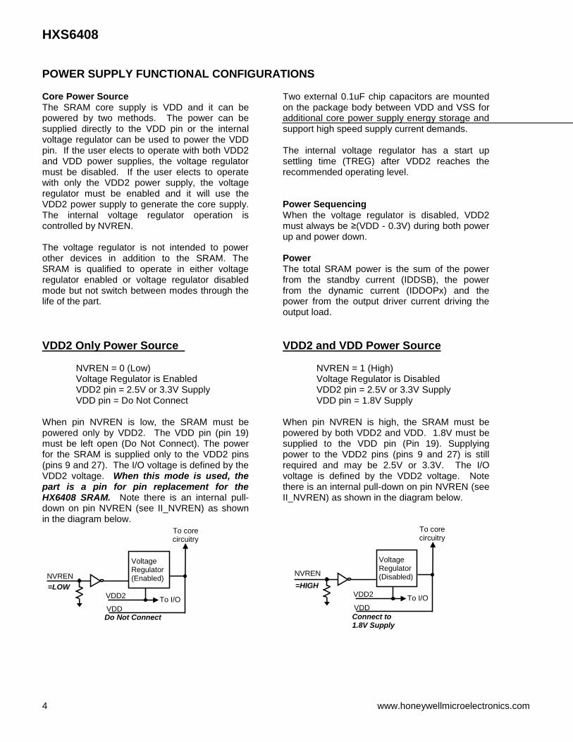
POWER SUPPLY FUNCTIONAL CONFIGURATIONS Core Power Source The SRAM core supply is VDD and it can be powered by two methods. The power can be supplied directly to the VDD pin or the internal voltage regulator can be used to power the VDD pin. If the user elects to operate with both VDD2 and VDD power supplies, the voltage regulator must be disabled. If the user elects to operate with only the VDD2 power supply, the voltage regulator must be enabled and it will use the VDD2 power supply to generate the core supply. The internal voltage regulator operation is controlled by NVREN. The voltage regulator is not intended to power other devices in addition to the SRAM. The SRAM is qualified to operate in either voltage regulator enabled or voltage regulator disabled mode but not switch between modes through the life of the part.
Two external 0.1uF chip capacitors are mounted on the package body between VDD and VSS for additional core power supply energy storage and support high speed supply current demands. The internal voltage regulator has a start up settling time (TREG) after VDD2 reaches the recommended operating level. Power Sequencing When the voltage regulator is disabled, VDD2 must always be ≥(VDD - 0.3V) during both power up and power down. Power The total SRAM power is the sum of the power from the standby current (IDDSB), the power from the dynamic current (IDDOPx) and the power from the output driver current driving the output load.
VDD2 Only Power Source NVREN = 0 (Low)
Voltage Regulator is Enabled VDD2 pin = 2.5V or 3.3V Supply VDD pin = Do Not Connect
When pin NVREN is low, the SRAM must be powered only by VDD2. The VDD pin (pin 19) must be left open (Do Not Connect). The power for the SRAM is supplied only to the VDD2 pins (pins 9 and 27). The I/O voltage is defined by the VDD2 voltage. When this mode is used, the part is a pin for pin replacement for the HX6408 SRAM. Note there is an internal pull-down on pin NVREN (see II_NVREN) as shown in the diagram below.
VDD2 and VDD Power Source NVREN = 1 (High) Voltage Regulator is Disabled VDD2 pin = 2.5V or 3.3V Supply VDD pin = 1.8V Supply
When pin NVREN is high, the SRAM must be powered by both VDD2 and VDD. 1.8V must be supplied to the VDD pin (Pin 19). Supplying power to the VDD2 pins (pins 9 and 27) is still required and may be 2.5V or 3.3V. The I/O voltage is defined by the VDD2 voltage. Note there is an internal pull-down on pin NVREN (see II_NVREN) as shown in the diagram below.
Voltage Regulator (Disabled)
VDD
VDD2
NVREN
=HIGH
To core circuitry
To I/O
Connect to 1.8V Supply
Voltage Regulator (Enabled)
VDD
VDD2
NVREN
Do Not Connect
=LOW
To core circuitry
To I/O
HXS6408
www.honeywellmicroelectronics.com 5
RADIATION HARDNESS RATINGS (1)
Symbol Parameter Environment Conditions Limits Unit
Neutron Irradiation Damage 1 MeV equivalent energy 1x10¹⁴
n/cm2
(1) Device will not latchup when exposed to any of the specified radiation environments.
(2) Calculated using CREME96.
RADIATION CHARACTERISTICS Total Ionizing Dose Radiation The S150 SRAM radiation hardness assurance TID level was qualified by
60Co testing, including
overdose and accelerated annealing, per MIL-STD-883 Method 1019. Ongoing assurance is provided by wafer level X-ray testing during manufacturing. Single Event Soft Error Rate Special process, memory cell, circuit and layout design considerations are included in the SRAM to minimize the impact of heavy ion and proton radiation and achieve small projected SER. These techniques sufficiently harden the SRAM such that cell redundancy and scrubbing are not required to achieve the projected SER. Transient Dose Rate Ionizing Radiation Many aspects of product design are addressed to handle the high energy levels associated with the transient dose rate events. This allows the SRAM to be capable of writing, reading, and retaining stored
data during and after exposure to a transient dose rate ionizing radiation pulse, up to the DRU specification. The SRAM will also meet functional and timing specifications after exposure to a transient dose rate ionizing radiation pulse up to the DRS specification. Neutron Irradiation Damage SOI CMOS is inherently tolerant to damage from neutron irradiation. The SRAM meets functional and timing specifications after exposure to the specified neutron fluence. Latchup The SRAM will not latchup when exposed to any of the above radiation environments when applied under recommended operating conditions. SOI CMOS provides oxide isolation between adjacent PMOS and NMOS transistors and eliminates any potential SCR latchup structures.
PIN CAPACITANCE (1)
Symbol Parameter Max Unit
CA Address Pin Capacitance 7 pF
CNOE NOE Pin Capacitance 17 pF
CNWE NWE Pin Capacitance 17 pF
CNCS NCS Pin Capacitance 20 pF
CDQ Data I/O Pin Capacitance 7 pF
(1) Maximum capacitance is verified as part of initial qualification only.
HXS6408
6 www.honeywellmicroelectronics.com
POWER PIN ELECTRICAL CHARACTERISTICS
Symbol Parameter Conditions Max Unit
Voltage Regulator Disabled
Voltage Regulator Enabled
VDD VDD2 VDD VDD2
IDDSB (1) Static
Supply Current
VIH = VDD2,
VIL = VSS,
DQ = High-Z
TA=25°C,
pre-TID 2 0.2 NA 2 mA
12 0.2 NA 12 mA
IDDOPW (2)(3) Dynamic
Supply Current
Selected, Write
VIH = VDD2,
VIL = VSS,
DQ = High-Z
1MHz 1.25 0.15 NA 1.25 mA
2MHz 2.5 0.3 NA 2.5 mA
10MHz 10 1.5 NA 10 mA
25MHz 25 3.8 NA 25 mA
40MHz 40 6.0 NA 40 mA
50MHz 50 7.5 NA 50 mA
IDDOPR (2)(3) Dynamic
Supply Current
Selected, Read
VIH = VDD2,
VIL = VSS,
DQ = High-Z
1MHz 0.75 0.125 NA 0.75 mA
2MHz 1.5 0.25 NA 1.5 mA
10MHz 6.0 1.25 NA 6.0 mA
25MHz 15 3.13 NA 15 mA
40MHz 24 5.0 NA 24 mA
50MHz 30 6.25 NA 30 mA
IDDOPD (2)(3) Dynamic
Supply Current
Deselected
VIH = VDD2,
VIL = VSS,
DQ = High-Z
1 MHz 0.1 0.1 NA 0.1 mA
40MHz 1 4 NA 5 mA
IDRRD Data Retention Supply
Current, Voltage
Regulator Disabled
VDD = 1V,
VDD2 = 2V
TA=25°C,
pre-TID 1 1 NA NA mA
10 1 NA NA mA
IDRRE (4) Data Retention Supply
Current, Voltage
Regulator Enabled
VDD2 = 2V TA=25°C,
pre-TID NA NA NA 2 mA
NA NA NA 11 mA
(1) See figure “ Typical IDD Standby Current, Pre-TID” for typical pre-TID current values. This is provided for information only.
(2) All inputs switching. DC average current.
(3) All dynamic operating mode current measurements (IDDOPx) exclude standby mode current (IDDSB).
(4) Guaranteed, but not tested.
SIGNAL PIN ELECTRICAL CHARACTERISTICS (1)
Symbol Parameter Conditions Min Max Unit
IIN (2) Input Leakage Current VSS ≤ VIN ≤ VDD2 -5 5 uA
IIH_NVREN NVREN Input Pull-Down Current NVREN = VDD2 200 700 uA
IOZ Output Leakage Current DQ = High-Z -10 10 uA
VIL Low-Level Input Voltage 0.3 x VDD2 V
VIH High-Level Input Voltage 0.7 x VDD2 V
VOL1 Low-Level Output Voltage for 3.3V I/O IOL = 10mA 0.4 V
VOH1 High-Level Output Voltage for 3.3V I/O IOH = -5mA 2.7 V
VOL2 (3) Low-Level Output Voltage for 2.5V I/O IOL = 10mA 0.4 V
VOH2 (3) High-Level Output Voltage for 2.5V I/O IOH = -5mA 2.0 V
(1) Voltages referenced to VSS.
(2) Excluding the NVREN pin.
(3) Guaranteed, but not tested.
HXS6408
www.honeywellmicroelectronics.com 7
READ CYCLE AC TIMING CHARACTERISTICS (1)(2)
Symbol Parameter Limits
2.5V I/O
Limits
3.3V I/O
Unit
Min Max Min Max
TAVAVR Read Cycle Time 16.5 15 ns
TAVQV Address Valid to Output Valid Access Time 16.5 15 ns
TAXQX Address Change to Output Invalid Time 5 5 ns
TSLQV Chip Select to Output Valid Access Time 16.5 15 ns
TSLQX Chip Select to Output Low-Z Time 0 0 ns
TSHQZ Chip Select to Output High-Z Time 2 2 ns
TGLQV Output Enable to Output Valid Access Time 5 4 ns
TGLQX Output Enable to Output Low-Z Time 0.5 0.5 ns
TGHQZ Output Enable to Output High-Z Time 3 3 ns
(1) The AC timing specifications are referenced to the AC Timing Input and Output References diagram and the Reference Load Circuit diagram. IBIS models should be used to evaluate timing under application load circuits.
(2) NWE = High
READ CYCLE AC TIMING WAVEFORMS
0
1
2
3
4
5
6
7
8
9
10
0 20 40 60 80 100 120 140
Cu
rre
nt (m
A)
Temperature (Degrees C)
Typical IDD Standby Current , Pre-TID
A
Q
T AVAVR
T AVQV T SLQV
T SLQX
NCS
T SHQZ
DATA VALID
T AXQX
HIGH-Z
NOE
T GHQZ T GLQX T GLQV
HXS6408
8 www.honeywellmicroelectronics.com
WRITE CYCLE AC TIMING CHARACTERISTICS (1)(2)(3)
Symbol Parameter Limits
2.5V I/O
Limits
3.3V I/O
Unit
Min Max Min Max
TAVAVW Write Cycle Time 10 10 ns
TWLWH Start of Write to End of Write Pulse Width 6 6 ns
TSLWH Chip Select to End of Write Time 7 7 ns
TDVWH Data Input Valid to End of Write Time 5 5 ns
TAVWH Address Valid to End of Write Time 7 7 ns
TWHDX Data Input Hold after End of Write Time 0 0 ns
TAVWL Address Valid Setup to Start of Write Time 0 0 ns
TWHAX Address Valid Hold after End of Write Time 0 0 ns
TWLQZ Start of Write to Output High-Z Time 2.5 2 ns
TWHQX End of Write to Output Low-Z Time 1 1 ns
TWHWL End of Write to Start of Write Pulse Width 4 4 ns
(1) The AC timing specifications are referenced to the AC Timing Input and Output References diagram and the
Reference Load Circuit diagram. IBIS models should be used to evaluate timing under application load circuits.
(2) For an NWE controlled write, NCS must be Low when NWE is Low.
(3) Can use NOE = High to hold Q in a High-Z state when NWE = High and NCS = Low.
WRITE CYCLE AC TIMING WAVEFORMS
T WHAX
HIGH-Z
T AVWL
T WHWL
T WHQX
D
T DVWH
T
A
Q
T AVWH
T WLQZ
T WHDX
DATA VALID
NWE
T WLWH
SLWH
T AVAVW
NCS
HIGH-Z
T SLQX T SHQZ
HXS6408
www.honeywellmicroelectronics.com 9
FUNCTIONAL DESCRIPTION SRAM Operation SRAM operation is asynchronous. Operating modes are defined in the Truth Table. Read operations can be controlled by Address (A(0-18)) or Chip Select (NCS). Write operations can be controlled by Write Enable (NWE) or Chip Select (NCS). Read Operation A read operation occurs when Chip Select (NCS) is low and Write Enable (NWE) is high. The output drivers are controlled independently by the Output Enable (NOE) signal. To control a read cycle with NCS where TSLQV is the access time, all addresses must be valid TAVQV minus TSLQV prior to the enabling NCS transition. Address transitions can occur later; however, the valid Data Output (Q) access time will then be defined by TAVQV instead of TSLQV. NCS can disable the read at any time; however, Data Output drivers will enter a High-Z state TSHQZ later. To control a read cycle with Address where TAVQV is the access time, NCS must transition low TSLQV minus TAVQV prior to the last Address transition. The NCS transition low can occur later; however, the valid Data Output (Q) access time will then be defined by TSLQV instead of TAVQV. To perform consecutive read cycles, NCS is held continuously low, and the toggling of any Address will start a new read cycle. Any amount of toggling or skew between Address transitions is permissible; however, Data Output will not become valid until TAVQV following the last occurring Address transition. The minimum Address activated read cycle time is TAVAVR which is the time between the last Address transition of the previous cycle and the first Address transition of the next cycle. The valid Data Output from a previous cycle will remain valid until TAXQX following the first Address transition of the next cycle. Write Operation A write operation occurs when Write Enable (NWE) is low and Chip Select (NCS) is low. Either NWE or NCS can start the write mode and either can end the write mode, but the write operation itself is defined by the overlap of NCS low and NWE low. Both modes of control are similar, except the NCS controlled mode disables the SRAM when NCS is high between writes. NWE/NCS controls the start of write when NCS/NWE transitions low before NWE/NCS transitions low. NWE/NCS controls the end of write when NCS/NWE transitions high after NWE/NCS transitions high.
To write Data (D) into the SRAM, NWE and NCS must be held low for at least TWLWH and TSLSH respectively. Any amount of skew between these signal transitions can be tolerated, and either one of these control signals can start or end the write operation as long as TSLWH and TWLSH are met. Address inputs must be valid at least TAVWL/TAVSL before the start of write from an NWE/NCS transition low and TAVWH/TAVSH before the end of write from an NWE/NCS transition high and must remain valid during the write operation. Hold times for address inputs with respect to the end of write from a NWE/NCS transition high must be a minimum of TWHAX/TSHAX. A Data Input (D) valid to the end of write time from an NWE/NCS transition high of TDVWH/TDVSH must be provided during the write operation. Hold times for Data Input with respect to the disabling NWE/NCS transition high must be at least TWHDX/TSHDX. To avoid Data Input driver contention with the SRAM output driver, the Data Input (D) must not be applied until TWLQZ/TGHQZ after the output drive (Q) is put into a High-Z condition by NWE/NOE. Consecutive write cycles are performed by toggling at least one of the NCS or NWE control signals high for TWHWL/TSHSL. If only one of these signals is used, the other must be in its write enable state (NWE or NCS held low). The minimum NWE/NCS write cycle time is TAVAVW/TAVAVS. Signal Integrity As a general design practice, one should have good signal integrity which means input signals that are free of noise, glitches and ringing with rising and falling edges of ≤10ns. More specifically, an input is considered to have good signal integrity when the input voltage monotonically traverses the region between VIL and VIH in ≤10ns. This is especially important in a selected and enabled state. When the device is selected and enabled, the last transitioning input for the desired operation must have good signal integrity to maintain valid operation. The transitioning inputs that bring the device into and out of a selected and enabled state must also have good signal integrity to maintain valid operation. When the device is deselected and/or disabled, inputs can have poor signal integrity and even float as long as the inputs that are defining the deselected and/or disabled state stay within valid VIL and VIH voltage levels. However, floating inputs for an extended period of time is not recommended.
HXS6408
10 www.honeywellmicroelectronics.com
RELIABILITY
For many years Honeywell has been producing integrated circuits that meet the stringent reliability requirements of space and defense systems. Honeywell has delivered hundreds of thousands of QML parts since first becoming QML qualified in 1990. Using this proven approach Honeywell will assure the reliability of the products manufactured with the SOI CMOS process technology. This approach includes adhering to Honeywell’s Quality Management Plan for:
• Designing in reliability by establishing electrical rules based on wear out mechanism characterization performed on specially designed test structures (electromigration, TDDB, hot carriers, bias temperature instability and radiation).
• Utilizing a structured and controlled design process.
• Statistically controlling wafer fabrication process with a continuous defect reduction process.
• Performing individual wafer lot acceptance through process monitor testing (includes radiation testing).
• Using characterized and qualified packages.
• Performing thorough product testing program based on MIL-PRF-38535 and MIL-STD 883.
SCREENING AND CONFORMANCE INSPECTION
The product test flow includes screening units with the applicable flow (Engineering Model, QML V, QML Q, Class V and Q equivalent) and the appropriate periodic or lot conformance testing (Groups A, B, C, D, and E). Both the wafer process and the products are subject to periodic or lot based Technology Conformance Inspection (TCI) and Quality Conformance Inspection (QCI) tests as defined by Honeywell’s Quality Management Plan.
Conformance Summary
Group A General Electrical Tests
Group B Mechanical – Resistance to Solvents, Bond Strength, Die Shear, Solderability
Group C Life Tests - 1000 hours at 125C or equivalent
Group D Package Related Mechanical Tests – Physical Dimensions, Lead Integrity, Thermal Shock, Temp Cycle, Moisture Resistance, Seal, Mechanical Shock, Vibration, Acceleration, Salt Atmosphere, Internal Water Vapor, Adhesion of Lead Finish
Group E Radiation Tests
REFERENCE LOAD CIRCUIT
DUT Output
30pF (1)
50ohm
Zo = 50ohm
VDD2/2
AC TIMING INPUT AND OUTPUT REFERENCES
Input Levels (1)
Output Levels
VDD2/2 (2)
High-Z (4)
High-Z (4)
VDD2
VSS
90%
10%
90%
10%
VOHss - 0.1V (2)(3)
VOLss + 0.1V (2)(3)
VDD2/2 (2)
VOHss - 0.1V (2)(3)
VOLss + 0.1V (2)(3)
Notes
(1) Input rise and fall times = 1ns between the 90% and 10% levels.
(2) Timing parameter reference voltage level.
(3) ss: Low-Z VOH and VOL steady-state output voltage.
(4) High-Z output pin pulled to VDD2/2 by Reference Load Circuit.
Notes (1) Set to 5pF for T*QZ (Low-Z to High-Z)
timing parameters.
HXS6408
11 www.honeywellmicroelectronics.com
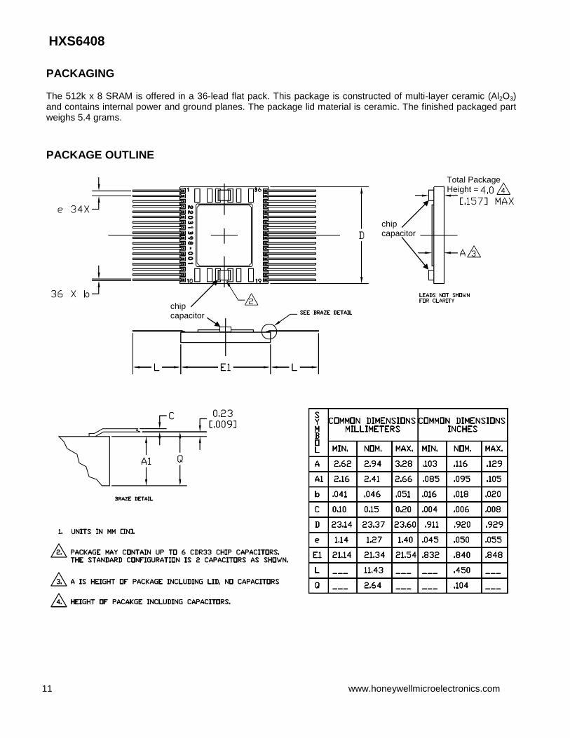
PACKAGING The 512k x 8 SRAM is offered in a 36-lead flat pack. This package is constructed of multi-layer ceramic (Al2O3) and contains internal power and ground planes. The package lid material is ceramic. The finished packaged part weighs 5.4 grams. PACKAGE OUTLINE
chip capacitor
Total Package Height =
chip capacitor
HXS6408
12
ORDERING INFORMATION (1) Standard Microcircuit Drawing The HXSR6408 SRAM can be ordered under the SMD drawing 5962-08215.
(1) Orders may be faxed to 763-954-2051. Please contact our Customer Service Representative at 1-800-323-8295 for further information.
(2) Engineering Model Description: Engineering Model suffix for Screening Level and Total Dose Hardness shall be “EN”. Parameters are tested -55°C to 125°C, 24 hour burn-in, no radiation hardness guaranteed.
(3) Contact Honeywell regarding details of bare die deliverables. For more information about Honeywell’s family of radiation hardened integrated circuit products and services, visit www.honeywellmicroelectronics.com.
This product and related technical data is subject to the U.S. Department of State International Traffic in Arms Regulations (ITAR) 22 CFR 120-130 and may not be exported, as defined by the ITAR, without the appropriate prior authorization from the Directorate of Defense Trade Controls, United States Department of State. Diversion contrary to U.S. export laws and regulations is prohibited. This datasheet includes only basic marketing information on the function of the product and therefore is not considered technical data as defined in 22CFR 120.10. Honeywell reserves the right to make changes of any sort without notice to any and all products, technology and testing identified herein. You are advised to consult Honeywell or an authorized sales representative to verify that the information in this data sheet is current before ordering this product. Absent express contract terms to the contrary, Honeywell does not assume any liability of any sort arising out of the application or use of any product or circuit described herein; nor does it convey any license or other intellectual property rights of Honeywell or of third parties.