JNTU SYLLABUS JAWAHARLAL NEHRU TECHNOLOGICAL UNIVERSITY HYDERABAD III Year B.Tech. ECE I - Sem L T/P/D C - -/3/- 2 (A50488) IC APPLICATIONS AND HDL SIMULATION LAB Note: To perform any sixteen experiments (choosing at least seven from each part). Part - I: Linear IC Experiments 1. OP AMP Applications – Adder, Subtractor, Comparators. 2. Integrator and Differentiator Circuits using IC 741. 3. Active Filter Applications – LPF, HPF (first order) 4. IC 741 Waveform Generators - Sine, Square wave and Triangular waves. 5. IC 555 Timer - Monostable and Astable Multivibrator Circuits. 6. Schmitt Trigger Circuits - Using IC 741 7. IC 565 - PLL Applications. 8. Voltage Regulator using IC 723, Three Terminal Voltage Regulators - 7805, 7809, 7912. EQUIPMENT REQUIRED: 1. 20 MHz / 40 MHz / 60 MHz Oscilloscope. 2. 1 MHz Function Generator (Sine, Square, Triangular and TTL). 3. Regulated Power Supply. 4. Multimeter / Volt Meter. Part - II: HDL Simulation programs: Programming can be done using any compiler. Download the programs on FPGA / CPLD boards and performance testing may be
Transcript
JNTU SYLLABUS
JAWAHARLAL NEHRU TECHNOLOGICAL UNIVERSITY HYDERABAD III Year B.Tech. ECE I - Sem L T/P/D C
- -/3/- 2(A50488) IC APPLICATIONS AND HDL SIMULATION LAB
Note: To perform any sixteen experiments (choosing at least seven from each part).
Part - I: Linear IC Experiments
1. OP AMP Applications – Adder, Subtractor, Comparators. 2. Integrator and Differentiator Circuits using IC 741.
3. Active Filter Applications – LPF, HPF (first order)
4. IC 741 Waveform Generators - Sine, Square wave and Triangular waves.
5. IC 555 Timer - Monostable and Astable Multivibrator Circuits.
6. Schmitt Trigger Circuits - Using IC 741
7. IC 565 - PLL Applications.
8. Voltage Regulator using IC 723, Three Terminal Voltage Regulators - 7805, 7809, 7912.
EQUIPMENT REQUIRED:
1. 20 MHz / 40 MHz / 60 MHz Oscilloscope.2. 1 MHz Function Generator (Sine, Square, Triangular and TTL).
3. Regulated Power Supply.
4. Multimeter / Volt Meter.
Part - II: HDL Simulation programs:
Programming can be done using any compiler. Download the programs on FPGA / CPLD boards and performance testing may be done using pattern generator / logic analyzer apart from verification by simulation using Cadence / Mentor Graphics / Synopsys / Equivalent front end CAD tools.
1. HDL code to realize all the logic gates2. Design of 2-to-4 decoder
3. Design of 8-to-3 encoder (without and with Priority)
4. Design of 8-to-1 multiplexer and 1 x 8 de multiplexer.
5. Design of 4 bit binary to gray code converter
6. Design of 4 bit comparator
IC APPLICATIONS AND HDL SIMULATION LAB
7. Design of Full adder using 3 modeling styles
8. Design of flip flops: SR, JK, T
9. Design of 4-bit binary, BCD counters (synchronous/ asynchronous reset)
10. Finite State Machine Design
LIST OF EXPERIMENTS:
Part - I: Linear IC Experiments
1. OP AMP Applications – Adder, Subtractor, Comparators. 2. Integrator and Differentiator Circuits using IC 741.3. Active Filter Applications – LPF, HPF (first order) 4. IC 741 Waveform Generators - Sine, Square wave and Triangular waves.5. IC 555 Timer - Monostable and Astable Multivibrator Circuits.6. Schmitt Trigger Circuits - Using IC 7417. IC 565 - PLL Applications.8. Voltage Regulator using IC 723, Three Terminal Voltage Regulators - 7805, 7809, 7912.
Part - II: HDL Simulation programs:
Programming can be done using any compiler. Download the programs on FPGA / CPLD boards and performance testing may be done using pattern generator / logic analyzer apart from verification by simulation using Cadence / Mentor Graphics / Synopsys / Equivalent front end CAD tools.
1. HDL code to realize all the logic gates2. Design of 2-to-4 decoder
3. Design of 8-to-3 encoder (without and with Priority)
4. Design of 8-to-1 multiplexer and 1 x 8 de-multiplexer.
5. Design of 4 bit binary to gray code converter
6. Design of 4 bit comparator
7. Design of Full adder using 3 modeling styles
8. Design of flip flops: SR, JK, T
9. Design of 4-bit binary, BCD counters (synchronous/ asynchronous reset)
10. Finite State Machine Design
Part - III: Additional Experiments
Department of ECE Page | 2
IC APPLICATIONS AND HDL SIMULATION LAB
1. 16x1 Multiplexer 74150 2. 4 bit DAC using op amp IC 741
Part - IV: Design Experiment
1. Band pass filter using 741 IC. 2. Johnson / Ring counter using IC 7495.
Part - V: Open Experiment.
1. Application of op-amp 741 IC. 2. Design the 8 bit data transfer using MUX, DEMUX and other ICs.
LABORATOURY RULESDO’S DO’S NOT1.Be regular to the lab. 1. Do not exceed the voltage Rating.
2. Do not inter change the IC’s while doing the experiment.
2. Follow proper Dress Code. 3. Avoid loose connections and short circuits.
3. Maintain Silence. 4. Do not throw the connecting wires to floor.
4. Know the theory behind the experiment before coming to the lab.
5. Do not come late to the lab.
5. Identify the different leads or terminals or pins of the IC before making connection.
6. Do not panic if you don’t get the output.
6. Know the Biasing Voltage required for different families of IC’s and connect the power supply voltage and ground terminals to the respective pins of the IC’s.7. Know the Current and Voltage rating of the IC’s before using them in the experiment.8. Avoid unnecessary talking while doing the experiment.9. Handle the IC Trainer Kit properly.10. Mount the IC Properly on the IC Zif Socket.11. Keep the Table clean.12. Take a signature of the in charge before taking the kit/components.13. After the completion of the experiments switch off the power supply
Department of ECE Page | 3
IC APPLICATIONS AND HDL SIMULATION LAB
and return the apparatus.14. Arrange the chairs/stools and equipment properly before leaving the lab
Part - I: IC Applications - Experiments
Department of ECE Page | 4
IC APPLICATIONS AND HDL SIMULATION LAB
EXPERIMENT 1 :
OP AMP APPLICATIONS – ADDER, SUBTRACTOR, COMPARATORS.
Objective: To study the working of op- amp as adder, subtractor and comparator.
Apparatus: -
Bread board - 1.
Regulated power supply - 2
CRO - 1.
IC 741 - 1.
Resistors
1KΩ - 2.
10KΩ - 4.
3.3KΩ - 1
2.2KΩ - 1.
RPS - 1.
Connecting wires.
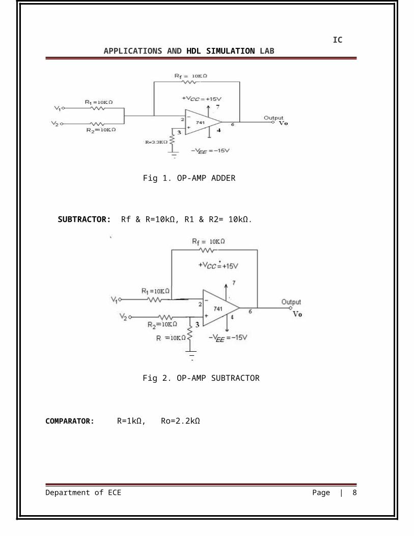
CIRCUIT DIAGRAMS:-
Department of ECE Page | 5
IC APPLICATIONS AND HDL SIMULATION LAB
ADDER Rf=10kΩ. R1=R2=10kΩ. R=3.3kΩ.
Fig 1. OP-AMP ADDER
SUBTRACTOR: Rf & R=10kΩ, R1 & R2= 10kΩ.
Fig 2. OP-AMP SUBTRACTOR
COMPARATOR: R=1kΩ, Ro=2.2kΩ
Department of ECE Page | 6
IC APPLICATIONS AND HDL SIMULATION LAB
Fig 3 comparator
PROCEDURE:-
ADDER
1. Connect the circuit as shown in the adder circuit diagram(fig 1).
2. . Apply the supply voltages of +15V to pin7 and -15V to pin4 of IC 741 respectively
3. Apply DC voltage from regulated power supply to inputs V1 and V2 .
4. Increase input voltages from 1V to 5V in steps of 1V for V1 and V2.
5. Note down the Vo corresponding inputs in CRO (DC mode).
6. Compare theoretical and practical values.
SUBTRACTOR
1. Connect the circuit as shown in the subtractor circuit diagram(fig 2).
2. . Apply the supply voltages of +15V to pin7 and -15V to pin4 of IC 741 respectively
3. Apply DC voltage from regulated power supply to inputs V1 and V2.Department of ECE Page | 7
IC APPLICATIONS AND HDL SIMULATION LAB
4. Keep the 5V at V1& slowly decrease V2 from 5V to 0V with six readings
5. Note down the Vo corresponding to different inputs in CRO( DC mode).
6. Compare theoretical and practical values.
COMPARATOR
1. Connect the circuit as shown in the figure 3.
2. . Apply the supply voltages of +15V to pin7 and -15V to pin4 of IC 741 respectively
3. Set the reference voltage as 1V DC.
4. Apply sine wave of 10Vp-p with1KHz frequency from the function generator as Vi.
5. Check the output on CRO and calculate the amplitude of the output wave form.
6. Plot the waveforms on graph sheets as shown in fig 4.
7. Compare the output wave form amplitude with input signal amplitude.
TABULAR FORMAT
ADDER
S.NO D.C Voltage at
input V1 (V)
D.C Voltage at
input V2 (V)
D.C Voltage at
Output VO (V)
1
2
3
4
5
6
7
Department of ECE Page | 8
IC APPLICATIONS AND HDL SIMULATION LAB
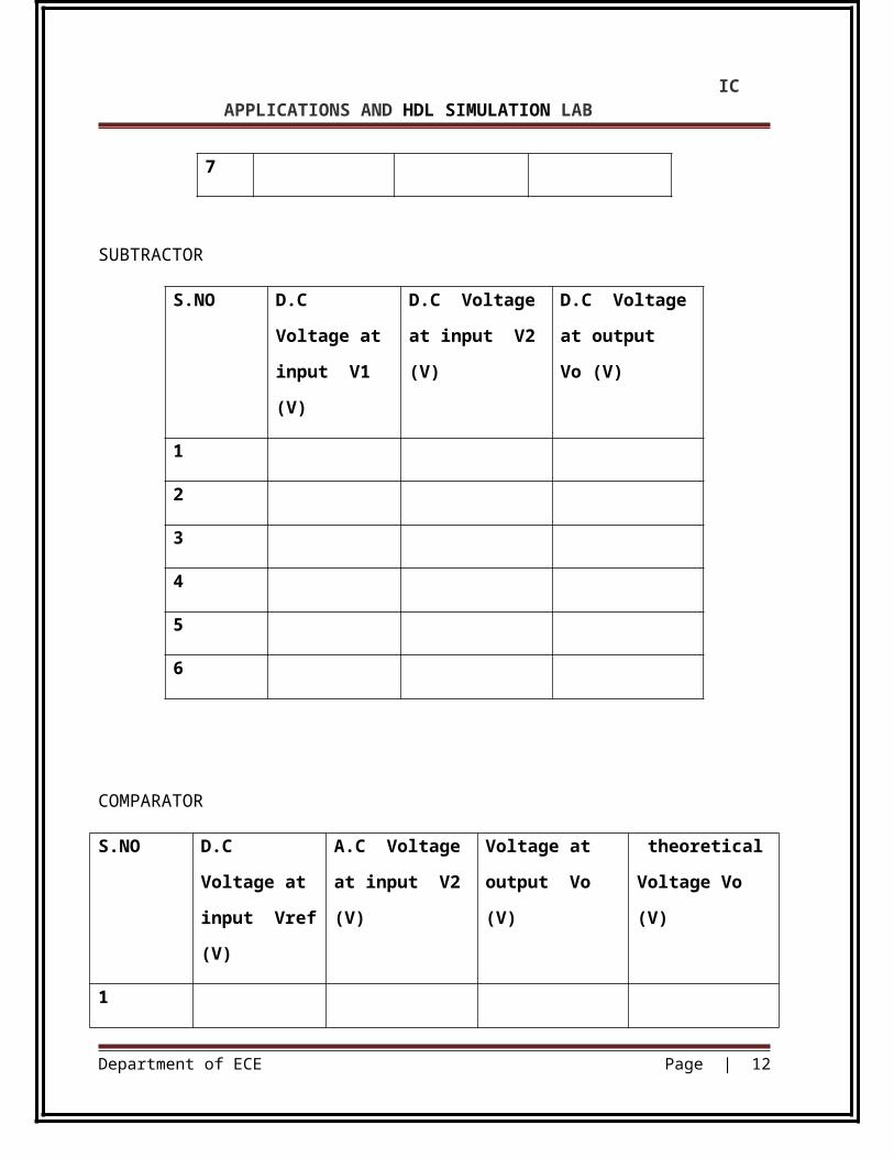
SUBTRACTOR
S.NO D.C Voltage at
input V1 (V)
D.C Voltage at
input V2 (V)
D.C Voltage at
output Vo (V)
1
2
3
4
5
6
COMPARATOR
S.NO D.C Voltage at
input Vref (V)
A.C Voltage at
input V2 (V)
Voltage at output
Vo (V)
theoretical
Voltage Vo (V)
1
2
EXPECTED WAVEFORMS
COMPARATOR
Department of ECE Page | 9
IC APPLICATIONS AND HDL SIMULATION LAB
Fig 4
RESULT: - Successfully constructed and studied the adder, subtractor and comparator circuits
using Op-Amp 741.
Outcome: After conducting this experiment students are able to design the circuits using op-
amps to perform addition, subtraction and comparison operations
Viva Questions:
1. Mention some of the linear applications of op – amps?
Adder, subtractor, voltage –to- current converter, current –to- voltage converters,
instrumentation amplifier, analog computation, power amplifier.
2. Mention some of the non – linear applications of op-amps? Rectifier, peak detector, clipper, clamper, sample and hold circuit, log amplifier, anti –
log amplifier, multiplier. 3. What happens when the common terminal of V+ and V- sources is not grounded?
Department of ECE Page | 10
IC APPLICATIONS AND HDL SIMULATION LAB
If the common point of the two supplies is not grounded, twice the supply voltage will
get applied and it may damage the op-amp.
4. What are ideal characteristics of an ideal op-amp?
Ideal characteristics of op-amp are
i. Open loop gain infinite ii. Input impedance infinite
iii. Output impedance lowiv. Bandwidth infinite
5. What is a comparator?
A comparator is a circuit which compares a signal voltage applied at one input of an op-amp with a known reference voltage at the other input. It is an open loop op - amp with output + Vsat.
6. Why IC 741 is not used for high frequency applications?
IC741 has a low slew rate because of the predominance of capacitance present in the circuit at higher frequencies. As frequency increases the output gets distorted due to limited slew rate.
EXPERIMENT 2 :
INTEGRATOR AND DIFFERENTIATOR USING IC 741 OP-AMP
OBJECTIVE: : -To study the working of op amp as differentiator and integrator.
2. Apply a bipolar symmetrical square wave of 2Vp-p amplitude and 1ms time period.
3. Connect the input and output of the circuit to channel 1and channel 2 of the CRO
respectively and observe the waveforms.
4. Draw the waveforms along with the levels on a graph.
5. Compare the practical values with theoretical values.
DIFFERENTIATOR
1. Connect the circuit as shown in fig 2.
2. Apply a bipolar symmetrical square wave of 2Vp-p amplitude and 1ms time period.
3. Connect the input and output of the circuit to channel 1and channel 2 of the CRO
respectively and observe the waveforms.
4. Draw the waveforms along with the levels on a graph.
5. Compare the practical values with theoretical values.
TABULER FORM
Integrator
sl.no
Input WaveformTime period
Amplitude Output waveform
amplitude Time period
1 Square wave (1KHz)
1ms 2Vp-p
2 Sine wave (1KHz)
1ms 2Vp-p
Differentiator Department of ECE Page | 13
IC APPLICATIONS AND HDL SIMULATION LAB
sl.no
Input WaveformTime period Amplitude Output
waveformamplitude Time
period
1 Square wave 1ms 2Vp-p Spike wave 0.19
MODEL WAVEFORMS:-
Integrating square wave
Integrating sine wave waveform
Department of ECE Page | 14
IC APPLICATIONS AND HDL SIMULATION LAB
Differentiator square wave
RESULT: - Successfully studied and observed differentiator and integrator circuits using
Op-Amp 741.
Outcome: After conducting this experiment students are able to design the circuits using op-
amps to perform integration and differentiation operations for different waveforms.
Viva:-
1. Define integrator.
Ans: An integrator is a device to perform the mathematical operation known as integration, a fundamental operation in calculus. The integration function is often part of engineering and scientific calculations. Mechanical integrators are used in such applications as metering of water flow or electric power. Electronic analog integrators were the basis of analog computers
1. Connect the circuit as shown in the lowpass filter circuit diagram (fig.1).
2. Apply 2V p-p sine wave input to the resistor R2 at Vin.
3. Keep the input constant and take any 10 readings of output voltage with 10 different
frequencies.
4. Observe the theoretical and practical voltage gains.
5. Draw the graph between voltage gain and frequency.
Department of ECE Page | 18
IC APPLICATIONS AND HDL SIMULATION LAB
TABULAR FORM:
S.No.
Input
frequency
(Hz)
Input
Amplitude
Vin (Vp-p)
Output
Amplitude
Vo (Vp-p)
Gain
Vo/Vin
Gain in
dB=20log (A)
1.
2.
3.
4.
5.
6.
7
8
9
10
HIGHPASS FILTER:
1. Connect the circuit as shown in the high pass filter circuit diagram(fig 2).
2. Apply 2V p-p sine wave input to the capacitor C2 at Vin.
3. Keep the input voltage constant and take any 10 readings of output voltage with 10
different frequencies.
4. Observe the theoretical and practical voltage gains.
5. Draw the graph between voltage gain and frequency.
TABLE:-
Department of ECE Page | 19
IC APPLICATIONS AND HDL SIMULATION LAB
S.No.
Input
frequency
(KHz)
Input
Amplitude
Vin (Vp-p)
Output
Amplitude
Vo(Vp-p)
Gain =Vo/Vin Gain in dB=20log
(A)
1.
2.
3.
4.
5.
6.
7
8
FREQUENCY RESPONSE PLOT :-
LOW PASS FILTER
HIGHPASS FILTER
Department of ECE Page | 20
IC APPLICATIONS AND HDL SIMULATION LAB
RESULT:-
Designed and observed the second order high pass and low pass filters for the given
specifications.
Outcome: After conducting these experiment students are able to design the Active filters understand the principles of filters and the difference between active and passive filters
VIVA :-
1.What are the different types of filters?
Ans: Based on functions: Lowpass filter, Highpass filter, Bandpass filter ,Bandreject filter.
Based on order of transfer function: first ,second, third higher order filters.
Based on configuration: Bessel, Chebychev, Butterworth filters.
2.Discuss the differences between Butterworth and Chebyshev filters?
Ans: Butterworth filter has flat frequency response in pass band where as chebyshev filter has
ripples in the pass band.
3.Give high cutoff frequency formula for the low pass filter?
Ans: Fh = 1/ 2π RC.
Department of ECE Page | 21
IC APPLICATIONS AND HDL SIMULATION LAB
4.What is the difference between analog filter and digital filter?
Ans: Analog filter has less performances whereas digital filters have good performances
5. Give low cutoff frequency formula for the high pass filter?
Ans: FL = 1/ 2π RC.
EXPERIMENT : 5
IC 555 TIMER - MONOSTABLE AND ASTABLE MULTIVIBRATOR CIRCUITS
OBJECTIVE: To design a monostable multivibrator having an output pulse width using
555 timer.
APPARATUS: -
Bread board - 1.
CRO - 1 .
IC 555 - 1.
Resistor
47KΩ - 2 .
Capacitors 0.01μF - 2.
RPS - 1
CIRCUIT DIAGRAM:-
R1=47K Ω, C1=0.01µF, C2=0.01µF
Department of ECE Page | 22
IC APPLICATIONS AND HDL SIMULATION LAB
Fig 1. Monostable multivibrator
Designing part:-
T = 1.1R1C1
Let C1=0.01µF & R1=47K Ω then T=0.5ms(approx)
PROCEDURE:-
Monostable multivibrator:-
1. Connect the circuit as shown in the circuit diagram Fig 1.
2. Apply Negative triggering pulses of frequency 1 KHz at pin 2.
3. Observe the output waveform at pin 3 and measure capacitor voltage across it at pin 6
4. Theoretically calculate the pulse duration as T=1.1. R1C1
5. Compare it with experimental values.
MODEL WAVEFORMS:-
Monostable multivibrator:-
Trigger input:-
Department of ECE Page | 23
IC APPLICATIONS AND HDL SIMULATION LAB
Capacitor and monostable output
RESULT:-
Successfully designed and verified the waveforms of monostable multivibrator
using 555 timer.
Outcome: After conducting these experiment students are able to design the monostable
multivibrator using IC 555 timer and understand the operation IC 555 timer
VIVA :-
1.Define duty cycle.
Ans: The ratio of high output and low output period is given by a mathematical parameter called duty cycle. It is defined as the ratio of ON Time to total time
2.Draw the pin diagram of 555 timers?
Ans:
Department of ECE Page | 24
IC APPLICATIONS AND HDL SIMULATION LAB
3.Explain the function of reset?
Ans: This pin is used to make the OUTPUT PIN (Pin 3) LOW. The reset pin must go below 0.7 volt and it needs 0.1mA to reset the chip. The RESET PIN is an overriding function. It will force the OUTPUT PIN to go LOW regardless of the state of the TRIGGER PIN (Pin 2). It can be used to terminate an output pulse prematurely, to gate oscillations from "on" to "off." The pin is active when a voltage level between 0v and 0.4 volt is applied to it. When not used, it is recommended that the RESET PIN is to be tied to the positive rail to avoid the possibility of false resetting.
4.What are the applications of 555 timers in monostable mode?
Ans: missing pulse detector, frequency divider, pulse width modulation.
5.What is the expression of %duty cycle in monostable mode?
Ans: %
6.Explain capacitor output waveform in monostable mode?
Ans: the capacitor gets charged upto maximum value of given signal whenever the input
changes suddenly from high to low level the capacitor slowly decrease, again for second pulse
input the capacitor charges from that value to the maximum value i.e 2/3 Vcc
7.Write down the expression for output pulse width in monostable mode?Ans: T = 1.1R1C1
Department of ECE Page | 25
IC APPLICATIONS AND HDL SIMULATION LAB
EXPERIMENT : 6
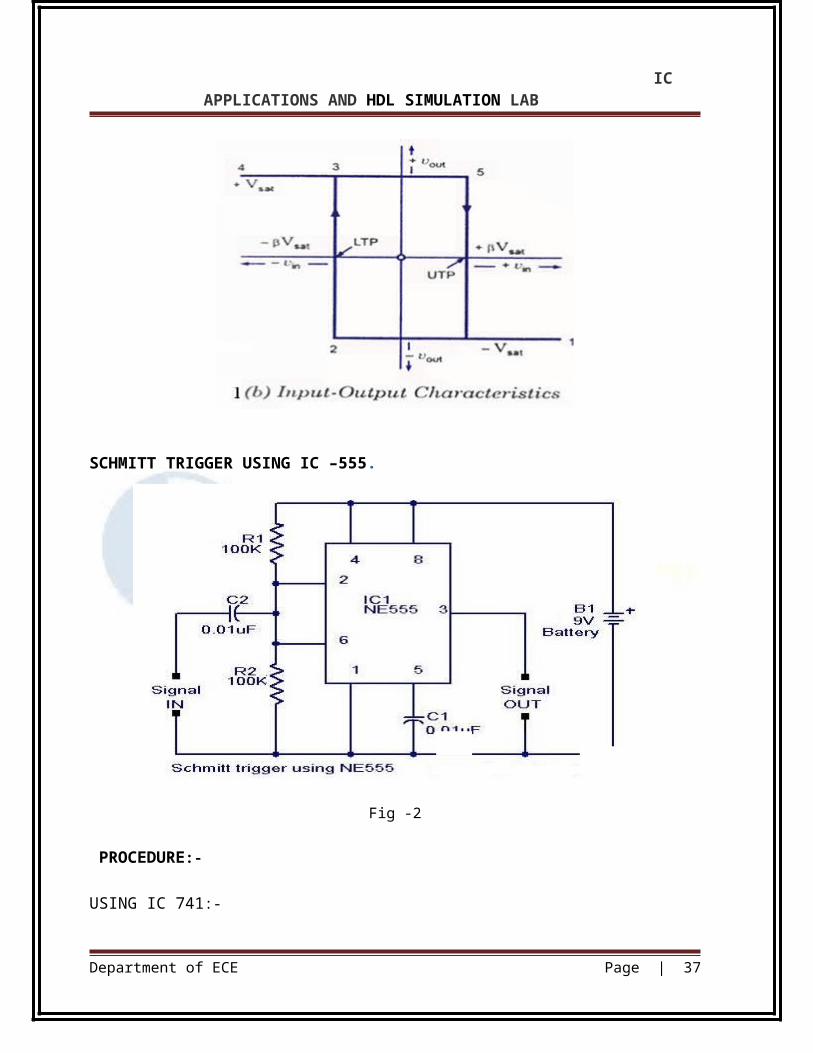
Schmitt Trigger Circuits - Using IC 741
OBJECTIVE: - To construct a Schmitt trigger circuit using IC 741 and IC 555,
verify the output wave forms
APPARATUS
Bread board - 1 No.
Regulated power supply - 1 No.
Function generator - 1 No.
CRO - 1 No.
IC 741 - 1 No.
Department of ECE Page | 26
IC APPLICATIONS AND HDL SIMULATION LAB
Resistors 100KΩ - 2 No.
1KΩ - 2 No.
10K Ω (pot) - 1 No
Capacitor 0.01μF - 2 No.
CIRCUIT DIAGRAM:-
FOR 741 IC
Fig 1(a). Schmitt trigger using IC 741
Department of ECE Page | 27
IC APPLICATIONS AND HDL SIMULATION LAB
SCHMITT TRIGGER USING IC –555.
Fig -2
PROCEDURE:-
USING IC 741:-
1. Connect the circuit as shown in fig 1(a) as Schmitt trigger using IC 741.
2. Give a 2V p-p sine wave of 1 kHz as input.
3. Observe the wave form on CRO and measure UTP and LTP.
4. Use x-y mode in CRO and observe hysteresis curve on CRO.
USING IC 555:-
1. Connect the circuit as shown in fig 2
2. Apply a sine wave of 1 KHz frequency of 2 V peak to peak at signal IN.
3. The output changes from - V sat to + V sat when the input crosses 2/3 Vcc it is the Upper
Trigger Point (UTP).
4. The output changes from +V sat to - Vsat when the input crosses 1/3 Vcc it is the Lower
Trigger Point (LTP).
5. Observe the output waveform on CRO and draw the relevant waveforms on graph
Sheet and note down the UTP and LTP values.
Department of ECE Page | 28
IC APPLICATIONS AND HDL SIMULATION LAB
MODEL WAVEFORMS:-
(a) input wave form , (b) output wave form
OBSERVATIONS:-
IC 741 IC 555
Parameter
Input Output
Input Output
Voltage( Vp-p),V
Time period(ms)
Parameter IC 741 IC 555Vutp
Vltp
RESULT: Constructed a Schmitt trigger circuits using IC 741 and IC 555 and verified the
output waveforms.
Department of ECE Page | 29
IC APPLICATIONS AND HDL SIMULATION LAB
Outcome: After conducting this experiment students are able to design the Schmitt trigger using IC 741 op amp and IC 555 timer.
VIVA:-
1. What are the circuits we used to generate square wave?
Ans: Schmitt trigger is a regenerative comparator. It converts sinusoidal input into a square wave output. The output of Schmitt trigger swings between upper and lower threshold voltages, which are the reference voltages of the input waveform.
9. What is the main application of schmitt trigger?Ans: When two levels are to be compared the may be oscillation at the border. Having hysteresis this problem is solved.
EXPERIMENT .7
IC 565-PLL APPLICATIONS
OBJECTIVE: - To study the operation of NE565 PLL.
APPARATUSES:-
Department of ECE Page | 31
IC APPLICATIONS AND HDL SIMULATION LAB
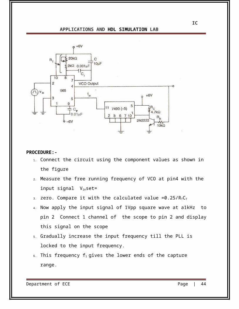
DC power supplyCROBread BoardFunction GeneratorResistor 6.8 kΩ – 1 No.Capacitor 0.1 µ F – 1 NoCapacitor 0.001 µ F – 2 NosIC565 - 1 No
THEO R Y : The 565 is available as a14-pin DIP package. It is produced by signatic corporation. The output frequency of the VCO can be rewritten as
Where RT and CT are the external resistor and capacitor connected to pin8 and pin9. A value between 2k and 20k is recommended for RT . The VCO free running frequency is adjusted with RT and CT to be at the centre for the input frequency range.
CIRCUIT DIAGRAM:
Department of ECE Page | 32
IC APPLICATIONS AND HDL SIMULATION LAB
PROCEDURE:-1. Connect the circuit using the component values as shown in the figure
2. Measure the free running frequency of VCO at pin4 with the input signal Vinset=
3. zero. Compare it with the calculated value =0.25/RTCT
4. Now apply the input signal of 1Vpp square wave at a1kHz to pin 2 Connect 1 channel
of the scope to pin 2 and display this signal on the scope
5. Gradually increase the input frequency till the PLL is locked to the input frequency.
6. This frequency f1 gives the lower ends of the capture range.
7. Go on increase the input frequency, till PLL tracks the input signal, say to a frequency
f2.
8. This frequency f2 gives the upper end of the lock range.
9. If the input frequency is increased further the loop will get unlocked.
10. Now gradually decrease the input frequency till the PLL is again locked. This is the
frequency f3, the upper end of the capture range . Keep on decreasing the input
frequency until the loop is unlocked. This frequency f4 gives the lower end of the lock
range
The lock range fL=(f2– f4) compare it with the calculated value of 0.78 Fo/ 12
Department of ECE Page | 33
IC APPLICATIONS AND HDL SIMULATION LAB
Also the capture range is fc=(f3– f1). Compare it with the calculated value of capture range
To use PLL as a multiplie5r, make connections as show in fig. The circuit uses a 4-bit binary
counter7490 used as a divide-by-5circuit.
Set the input signal at 1Vpp square wave at 500Hz
Vary the VCO frequency by adjusting the 20K potentiometer till the PLL is locked.
Measure the output frequency
Repeat step 9 and10 for input frequency of 1kHz and 1.5kHz.
GRAPH:
RESULT:
fo=
fL=
fC=
Department of ECE Page | 34
IC APPLICATIONS AND HDL SIMULATION LAB
Outcome: After conducting this experiment students are able to understand the applications of PLL.
QUESTIONS:
1.Define VCO?Ans: A voltage controlled oscillator is an oscillator circuit in which the frequency of oscillations can be controlled by an externally applied voltage.
2.List the features of 566 VCO?Ans: Wide supply voltage range(10-24V). Very linear modulation characteristics. High temperature stability.
3.What do u mean by PLL?Ans: A PLL is a basically a closed loop system designed to lock output frequency and phase to the frequency and phase of an input signal.
4.Define lock rangeAns: When PLL is in lock, it can trap freq changes in the incoming signal. The range of frequencies over which the PLL can maintain lock with the incoming signal is called as lock range.
5.Define pull-in time?Ans: The total time taken by the PLL to establish lock is called pull-in time.
6.Define capture range ?Ans: The range of frequencies over which the PLL can acquire lock with the input signal is called as capture range.
Department of ECE Page | 35
IC APPLICATIONS AND HDL SIMULATION LAB
EXPERIMENT. 8:-
Voltage Regulator using IC 723, Three Terminal Voltage Regulators - 7805, 7809, 7912
OBJECTIVE : - To study the voltage regulation characteristics and plot the response curve for line regulation and load regulation using 723 IC.
1. Connections are made as per the circuit diagram.2. Power supply is connected to12 and 7 terminals.3. Volt meter is connected to10 and 7 terminals.4. By increasing the input voltage corresponding volt meter reading is noted.
II. LOAD REGULATION
1. Connect the load to the terminals 10 and GND.2. Keep the input voltage constant at which line regulation is obtained3. The maximum load value is calculated from IC ratings.4. Now, we decrease the load resistance and note down the corresponding Of the output in volt meter.5.Plot the graph for load verses load regulation.
OBSERVATIONS:
Line regulation
Vnl=
Line voltage (V) Output voltage(V)
Department of ECE Page | 37
IC APPLICATIONS AND HDL SIMULATION LAB
Load regulation
Regulated output(V)
Load current(mA)
Load resistance(KΩ)
Load regulation
% REGULATION=[(Vnl-Vfl)/Vfl]*100
MODEL GRAPH
PRECAUTIONS:
1. While taking the readings of regulated output voltage load regulation ,keep the input voltage constant at15V.
2. Do not increase the input voltage more than 30 V while taking the reading for no load
condition?
RESULT: The load regulations and line regulations are observed by the IC 723.
Department of ECE Page | 38
IC APPLICATIONS AND HDL SIMULATION LAB
Outcome: After conducting this experiment students are able to use IC 723 as voltage regulator and understand its operation.
VIVA :-
1.What is meant by line regulation?
Ans: Line regulation is expressed as percent of change in the output voltage relative to the change in the input line voltage.
2.What is meant by load regulation ?
Ans: Load regulation is the capability to maintain a constant voltage (or current) level on the
output channel of a power supply despite changes in the resistor's load.
3.What is the % of load regulation?
Ans: Load Regulation can be defined as a percentage by the equation:
4.What is a voltage regulator?
Ans: A voltage regulator is an electronic circuit that provides a stable dc voltage independent of the load current, temperature, and ac line voltage variations .
5.What is a switching regulator?Ans: Switching regulators are those which operate the power transistor as a high frequency on/off switch, so that the power transistor does not conduct current continuously. This gives improved efficiency over series regulators.
6.What are the advantages of IC voltage regulators?Ans: Low cost , high reliability , reduction in size , excellent performance.
7.What is meant by current limiting?Ans: Current limiting refers to the ability of a regulator to prevent the load current from increasing above a preset value.
8.Give the drawbacks of linear regulatorsAns: The input step down transformer is bulky and expensive because of low line frequency Because of low line frequency, large values of filter capacitors are required to decrease the ripple. Efficiency is reduced due to the continuous power dissipation by the transistor as it operates in the linear region. 10. What is the advantage of switching regulators?Ans: Greater efficiency is achieved as the power transistor is made to operate as low impedance switch. Power transmitted across the transistor is in discrete pulses rather than as a steady current flow By using suitable switching loss reduction technique, the switching
frequency can be increased so as to reduce the size and weight of the inductors and capacitors.
Department of ECE Page | 40
GCET IC APPLICATIONS LAB MANUAL
OPEN EXPERIMENTS
EXPERIMENT:1
APPLICATIONS OF OP-AMPAIM: To study the application of op-amp.
APPARATUS:
IC 741 -1
Connecting wire.
Resistor 1kΩ -3
Ammeter -1
Voltmeter -1
THEORY:
The voltage-to-current converter, as shown in Figure 1 , produces an output current that depends on the input voltage and the resistor R. In particular, the output current Iout = Vi/R independent of the loading resistance RL.
The current-to-voltage converter, as shown in Figure 8-3, produces an output voltage that depends on the input current and the resistor R. In particular, the output voltage Vo = -IinR independent of the size of the loading resistance RL.
CIRCUITS DIAGRAM:
Department of ECE Page 41
GCET IC APPLICATIONS LAB MANUAL
Fig: 1 voltage to current converter
Fig: 2 current to voltage converter
PROCEDURE:
Part A: Op amp converter
i) Voltage-to-current converter
1. Connect the circuit of Figure 1
2. Adjust voltage supply Vin according to the value listed in Table1.
3. Record the result, iout correspondingly.
ii) Current-to-voltage converter
1. Connect the circuit of Figure 2.
2. Adjust the voltage supply Vin such that the current iin according to Table 2 is obtained.
3. Measure Vout and record the result in Table 8-2.
Department of ECE Page 42
GCET IC APPLICATIONS LAB MANUAL
TABLE 1: Voltage-to-current converter
s.no Voltage(Vi) Current(Io)
TABLE 2: Current-to-voltage converter
s.no Current(Ii) Voltage(Vo)
RESULT : The output to input values of current and voltage is observed and verified.
Department of ECE Page 43
GCET IC APPLICATIONS LAB MANUAL
EXPERIMENT:2
ENCODER AND DECODER
AIM:-To convert a given octal input to the binary output and to study the LED
display using 7447 7-segment decoder/ driver.
APPARATUS REQUIRED: -
IC 74148, IC 7447, 7-segment display, etc.
CIRCUIT DIAGRAM:
PROCEDURE : - (Encoder)
1. Connections are made as per circuit diagram.
2. The octal inputs are given at the corresponding pins.
3. The outputs are verified at the corresponding output pins.
Department of ECE Page 44
GCET IC APPLICATIONS LAB MANUAL
PROCEDURE: - (Decoder)
1. Connections are made as per the circuit diagram.
2. Connect the pins of IC 7447 to the respective pins of the LED display board.
3. Give different combinations of the inputs and observe the
decimal numbers displayed on the board.
RESULT: The given octal numbers are converted into binary numbers.
The given data is displayed using &-segment LED decoder
Department of ECE Page 45
GCET IC APPLICATIONS LAB MANUAL
APPENDIX -A
Pin Configuration:
Specifications:
1. Voltage gain A = α typically 2, 00,000
2. I/P resistance RL = α , practically 2M
3. O/P resistance R1 =0, practically 75
4. Bandwidth = α Hz. It can be operated at any frequency
5. Common mode rejection ratio = α (Ability of op amp to reject noise voltage)
6. Slew rate + α V/µsec(Rate of change of O/P voltage)
7. When V1 = V2, VD=0
8. Input offset voltage (Rs ≤ 10K) max 6 mv
Department of ECE Page 46
GCET IC APPLICATIONS LAB MANUAL
9. Input offset current = max 200nA
10. Input bias current: 500nA
11. Input capacitance: type value 1.4PF
12. Offset voltage adjustment range: ± 15mV
13. Input voltage range: ± 13V
14. Supply voltage rejection ratio : 150 µr/V
15. Output voltage swing: + 13V and - 13V for RL > 2K
16. Output short-circuit current: 25mA
17. Supply current: 28mA
18. Power consumption: 85MW
19. Transient response: rise time= 0.3 µs
20. Overshoot= 5%
APPENDIX - B
IC 555
Department of ECE Page 47
GCET IC APPLICATIONS LAB MANUAL
Specifications:
1. Operating temperature : SE 555 -55oC to 125oC
NE 555 0o to 70oC2. Supply voltage : +5V to +18V3. Timing : µSec to Hours4. Sink current : 200mA5. Temperature stability : 50 PPM/oC change in temp or 0-005% /oC
APPENDIX - C IC723 Pin Configuration
Specifications of 723:
Power dissipation : 1W
Input Voltage : 9.5 to 40V
Output Voltage : 2 to 37V
Output Current : 150mA for Vin-Vo = 3V
Department of ECE Page 48
GCET IC APPLICATIONS LAB MANUAL
10mA for Vin-Vo = 38V
Load regulation : 0.6% Vo
Line regulation : 0.5% Vo
REFERENCES
1. D. Roy Choudhury and Shail B.Jain, Linear Integrated Circuits, 2nd edition, New Age International .
2. Ramakant A. Gayakwad, Operational and Linear Integrated Circuits, 4th edition, PHI
3. S. Franco, Design with Operational Amplifiers and Analog Integrated Circuits, 3rd edition, TMH.
4. James M. Fiore, Operational Amplifiers and Linear Integrated Circuits: Theory and Application, WEST.
5. J.Milliman and H.Taub, Pulse and digital circuits, McGraw-Hill.
6. David A. Bell, Solid State Pulse circuits, PHI .
7. Roy Mancini, OPAMPs for Everyone, 2nd edition, Newnes.
8. Anand Kumar, Pulse and Digital Circuits, PHI .
9. William D. Stanley, Operational Amplifiers with Linear Integrated Circuits, 4th edition, Pearson.


![ECE 4514 Digital Design II Spring 2008 How HDL simulation ... cu FPGA CURS/lecture5[1].pdfa PC. HDL simulation is different from C execution Need to express concurrency (things happening](https://static.documents.pub/doc/80x56/5e2c01561daefc315a0e8847/ece-4514-digital-design-ii-spring-2008-how-hdl-simulation-cu-fpga-curslecture51pdf.jpg)


