ICM-20789 7-Axis, High Performance Integrated 6-Axis Inertial and Barometric Pressure Sensor InvenSense reserves the right to change the detail specifications as may be required to permit improvements in the design of its products. TDK Corporation 1745 Technology Drive, San Jose, CA 95110 U.S.A +1(408) 988–7339 www.invensense.com Document Number: DS-000169 Revision: 1.3 Revision Date: 10/31/2017 GENERAL DESCRIPTION The 7-Axis ICM-20789 is an integrated 6-axis inertial device that combines a 3-axis gyroscope, 3-axis accelerometer, and an ultra-low noise MEMS capacitive pressure sensor in a 24- pin LGA package. This unique 7-Axis device offers performance of discrete components in a single small footprint for tracking rotational and linear motion as well as pressure differences with an accuracy of ±1 Pa, an accuracy enabling altitude measurement differentials as small as 8.5 cm. The pressure sensor’s MEMS capacitive architecture provides the industry’s lowest noise at the lowest power, high sensor throughput, and temperature coefficient offset of ±0.5 Pa/°C. The pressure sensor’s combination of high accuracy elevation measurements, low power, and temperature stability complemented by the motion tracking 6-axis inertial sensor in a small footprint, make it ideal for a wide range of motion tracking applications. The embedded 6-axis MotionTracking device combines a 3- axis gyroscope, 3-axis accelerometer, and a Digital Motion Processor™ (DMP). An available large 4 kB FIFO reduces traffic on the serial bus interface, and power consumption through burst sensor data transmission. The Gyroscope has programmable FSR of ±250 dps, ±500 dps, ±1000 dps and ±2000 dps. The Accelerometer FSR is programmable to ±2g, ±4g, ±8g and ±16g ICM-20789 has 16-bit ADC for the 6-axis inertial sensor and 24-bit ADC for the pressure Sensor, programmable digital filters, two temperature sensors – one each in 6-axis Inertial and Pressure sensor. The device features an operating voltage of 1.8V. Communication port includes I 2 C at 400 kHz (6-axis and Pressure) and 8 MHz SPI (6-axis only). The package is 4x4x1.365 mm 24-pin to minimize board area requirements. BLOCK DIAGRAM APPLICATIONS • Drones and Flying Toys • Motion-based gaming controllers • Virtual Reality headsets and controllers • Indoor/Outdoor Navigation (dead-reckoning, floor/elevator/step detection) FEATURES • Pressure operating range: 30 to 110 kPa • Noise and current consumption o 3.2 Pa @ 1.3 µA (LP mode) o 0.8 Pa @ 5.2 µA (LN mode) o 0.4 Pa @ 10.4 µA (ULN mode) • Pressure Sensor Relative Accuracy: ±1 Pa for any 10 hPa change over 950 hPa-1050 hPa at 25°C • Pressure Sensor Absolute Accuracy: ±1 hPa over 950 hPa-1050 hPa, 0°C to 65°C • Pressure Sensor Temperature Coefficient Offset: ±0.5 Pa/°C over 25°C to 45°C at 100 kPa • Gyroscope programmable FSR of ±250 dps, ±500 dps, ±1000 dps, and ±2000 dps • Accelerometer with Programmable FSR of ±2g, ±4g, ±8g, and ±16g • Large 4 kB FIFO reduces traffic on the serial bus interface • EIS FSYNC support • User-programmable interrupts • Wake-on-motion interrupt for low power operation of applications processor • Host interface: 400 kHz Fast Mode I 2 C & 8 MHz SPI (see datasheet for ICM-20689) • Digital-output temperature sensor (x2) • Nominal VDD operation at 1.8V • RoHS and Green compliant ORDERING INFORMATION PART TEMP RANGE PACKAGE ICM-20789† −40°C to +85°C 24-Pin LGA †Denotes RoHS and Green-Compliant Package I 2 C AP/HUB ICM-20789 SPI (6-Axis only) 6-Axis Motion Pressure Sensor I 2 C I 2 C
Transcript
ICM-20789
7-Axis, High Performance Integrated 6-Axis Inertial and Barometric Pressure Sensor
InvenSense reserves the right to change the detail specifications as may be required to permit improvements in the design of its products.
TDK Corporation 1745 Technology Drive, San Jose, CA 95110 U.S.A
GENERAL DESCRIPTION The 7-Axis ICM-20789 is an integrated 6-axis inertial device that combines a 3-axis gyroscope, 3-axis accelerometer, and an ultra-low noise MEMS capacitive pressure sensor in a 24-pin LGA package. This unique 7-Axis device offers performance of discrete components in a single small footprint for tracking rotational and linear motion as well as pressure differences with an accuracy of ±1 Pa, an accuracy enabling altitude measurement differentials as small as 8.5 cm.
The pressure sensor’s MEMS capacitive architecture provides the industry’s lowest noise at the lowest power, high sensor throughput, and temperature coefficient offset of ±0.5 Pa/°C. The pressure sensor’s combination of high accuracy elevation measurements, low power, and temperature stability complemented by the motion tracking 6-axis inertial sensor in a small footprint, make it ideal for a wide range of motion tracking applications.
The embedded 6-axis MotionTracking device combines a 3-axis gyroscope, 3-axis accelerometer, and a Digital Motion Processor™ (DMP). An available large 4 kB FIFO reduces traffic on the serial bus interface, and power consumption through burst sensor data transmission. The Gyroscope has programmable FSR of ±250 dps, ±500 dps, ±1000 dps and ±2000 dps. The Accelerometer FSR is programmable to ±2g, ±4g, ±8g and ±16g
ICM-20789 has 16-bit ADC for the 6-axis inertial sensor and 24-bit ADC for the pressure Sensor, programmable digital filters, two temperature sensors – one each in 6-axis Inertial and Pressure sensor. The device features an operating voltage of 1.8V. Communication port includes I2C at 400 kHz (6-axis and Pressure) and 8 MHz SPI (6-axis only). The package is 4x4x1.365 mm 24-pin to minimize board area requirements.
BLOCK DIAGRAM
APPLICATIONS
• Drones and Flying Toys • Motion-based gaming controllers • Virtual Reality headsets and controllers • Indoor/Outdoor Navigation (dead-reckoning,
floor/elevator/step detection)
FEATURES
• Pressure operating range: 30 to 110 kPa • Noise and current consumption
o 3.2 Pa @ 1.3 µA (LP mode) o 0.8 Pa @ 5.2 µA (LN mode) o 0.4 Pa @ 10.4 µA (ULN mode)
• Pressure Sensor Relative Accuracy: ±1 Pa for any 10 hPa change over 950 hPa-1050 hPa at 25°C
• Pressure Sensor Absolute Accuracy: ±1 hPa over 950 hPa-1050 hPa, 0°C to 65°C
• Pressure Sensor Temperature Coefficient Offset: ±0.5 Pa/°C over 25°C to 45°C at 100 kPa
• Gyroscope programmable FSR of ±250 dps, ±500 dps, ±1000 dps, and ±2000 dps
• Accelerometer with Programmable FSR of ±2g, ±4g, ±8g, and ±16g
• Large 4 kB FIFO reduces traffic on the serial bus interface
• EIS FSYNC support • User-programmable interrupts • Wake-on-motion interrupt for low power operation
of applications processor • Host interface: 400 kHz Fast Mode I2C & 8 MHz SPI
(see datasheet for ICM-20689) • Digital-output temperature sensor (x2) • Nominal VDD operation at 1.8V • RoHS and Green compliant
ORDERING INFORMATION
PART TEMP RANGE PACKAGE ICM-20789† −40°C to +85°C 24-Pin LGA
†Denotes RoHS and Green-Compliant Package
I2C
AP/HUB
ICM-20789
SPI (6-Axis only)
6-Axis Motion Pressure
Sensor I2C
I2C
ICM-20789
Document Number: DS-000169 Page 2 of 62 Revision: 1.3
TABLE OF CONTENTS General Description ............................................................................................................................................. 1 Block Diagram ...................................................................................................................................................... 1 Applications ......................................................................................................................................................... 1 Features ............................................................................................................................................................... 1 Ordering Information ........................................................................................................................................... 1
4 Applications Information ................................................................................................................................... 17 4.1 Pin Out Diagram and Signal Description ................................................................................................. 17 4.2 Typical Operating Circuit ......................................................................................................................... 18 4.3 Bill of Materials for External Components .............................................................................................. 21 4.4 Block Diagram ......................................................................................................................................... 22 4.5 Overview ................................................................................................................................................. 23 4.6 Three-Axis MEMS Gyroscope with 16-bit ADCs and Signal Conditioning ............................................... 24 4.7 Three-Axis MEMS Accelerometer with 16-bit ADCs and Signal Conditioning ......................................... 24 4.8 Digital Motion Processor ......................................................................................................................... 24 4.9 Pressure Sensor ....................................................................................................................................... 24 4.10 I2C Serial Communications Interface .................................................................................................. 24 4.11 Self-Test .............................................................................................................................................. 25 4.12 Clocking ............................................................................................................................................... 26 4.13 Sensor Data Registers ......................................................................................................................... 26 4.14 FIFO ..................................................................................................................................................... 26 4.15 Interrupts ............................................................................................................................................ 26 4.16 Digital-Output Temperature Sensor ................................................................................................... 26
ICM-20789
Document Number: DS-000169 Page 3 of 62 Revision: 1.3
4.17 Bias and LDOs ..................................................................................................................................... 26 4.18 Charge Pump ...................................................................................................................................... 26 4.19 Standard Power Modes – Update the power modes ......................................................................... 27
10 Pressure sensor – How to Read ......................................................................................................................... 50 10.1 I2C Operation And Communication .................................................................................................... 50
12 Part Number Package Marking .......................................................................................................................... 58 13 Ordering Guide .................................................................................................................................................. 59 14 Reference ........................................................................................................................................................... 60 15 Revision History ................................................................................................................................................. 61
ICM-20789
Document Number: DS-000169 Page 5 of 62 Revision: 1.3
LIST OF FIGURES Figure 1. I2C Bus Timing Diagram ............................................................................................................................................................. 15 Figure 2. Pin out Diagram for ICM-20789 ................................................................................................................................................ 17 Figure 3. I2C Communication – 1.8V Supply Schematic ........................................................................................................................... 18 Figure 4. I2C Communication MCU Interface at 3V or 1.8V Schematic .................................................................................................... 19 Figure 5. SPI Communication for Gyro/Accel; I2C for Pressure Schematic .............................................................................................. 20 Figure 6. SPI Communication for Gyro/Accel; I2C Pressure; MCU Digital Interface: 1.8V Schematic ...................................................... 20 Figure 7. SPI Communication for Gyro/Accel; I2C for Pressure; MCU Digital Interface: 3.0V Schematic................................................. 21 Figure 8. ICM-20789 Block Diagram (I2C interface).................................................................................................................................. 22 Figure 9. ICM-20789 Block Diagram (SPI/ I2C interface) .......................................................................................................................... 23 Figure 10. ICM-20789 Solution Using I2C Interface .................................................................................................................................. 25 Figure 11. START and STOP Conditions .................................................................................................................................................... 29 Figure 12. Acknowledge on the I2C Bus ................................................................................................................................................... 30 Figure 13. Complete I2C Data Transfer ..................................................................................................................................................... 30 Figure 14. I/O Levels and Connections ..................................................................................................................................................... 33 Figure 15. Communication Sequence for starting a measurement and reading measurement results .................................................. 54 Figure 16. Orientation of Axes of Sensitivity and Polarity of Rotation .................................................................................................... 55 Figure 17. Package Dimensions................................................................................................................................................................ 56 Figure 18. ICM-20789 recommended PCB land pattern .......................................................................................................................... 57 Figure 19. Part Number Package Marking ............................................................................................................................................... 58
ICM-20789
Document Number: DS-000169 Page 6 of 62 Revision: 1.3
LIST OF TABLES Table 1. Gyroscope Specifications ............................................................................................................................................................. 9 Table 2. Accelerometer Specifications ..................................................................................................................................................... 10 Table 3. Operation Ranges ....................................................................................................................................................................... 11 Table 4. Operation Modes ....................................................................................................................................................................... 11 Table 5. Pressure Sensor Specifications ................................................................................................................................................... 11 Table 6. Temperature Sensor Specifications ............................................................................................................................................ 12 Table 7. D.C. Electrical Characteristics ..................................................................................................................................................... 12 Table 8. A.C. Electrical Characteristics (6-Axis) ........................................................................................................................................ 13 Table 9. Electrical Characteristics (Pressure sensor) ................................................................................................................................ 14 Table 10. Other Electrical Specifications .................................................................................................................................................. 14 Table 11. I2C Timing Characteristics ......................................................................................................................................................... 15 Table 12. Absolute Maximum Ratings (6-Axis) ........................................................................................................................................ 16 Table 13. Absolute Maximum Ratings (pressure sensor)......................................................................................................................... 16 Table 14. Signal Descriptions ................................................................................................................................................................... 17 Table 15. Bill of Materials ........................................................................................................................................................................ 21 Table 16. Standard Power Modes for ICM-20789.................................................................................................................................... 27 Table 17. Table of Interrupt Sources ........................................................................................................................................................ 28 Table 18. Serial Interface ......................................................................................................................................................................... 29 Table 19. I2C Term SPI Interface ............................................................................................................................................................... 31 Table 20. Register Map ............................................................................................................................................................................ 35 Table 21. Accelerometer Data Rates and Bandwidths (Low Noise Mode) .............................................................................................. 39 Table 22. Accelerometer Data Rates and Bandwidths (Low-Power Mode) ............................................................................................. 40 Table 23. ICM-20789 I2C Device Address ................................................................................................................................................. 50 Table 24. Measurement Commands ........................................................................................................................................................ 50 Table 25. Soft Reset Command ................................................................................................................................................................ 51 Table 26. Read-Out Command of ID Register .......................................................................................................................................... 51 Table 27. Structure of the 16-bit ID ......................................................................................................................................................... 51 Table 28. ICM-20789 I2C CRC Properties .................................................................................................................................................. 51 Table 29. Package Dimensions Table ....................................................................................................................................................... 56
ICM-20789
Document Number: DS-000169 Page 7 of 62 Revision: 1.3
1 INTRODUCTION 1.1 PURPOSE AND SCOPE This document is a product specification, providing a description, specifications, and design related information on the ICM-20789, a 6-axis inertial and pressure sensor device. The device is packaged in a 4 mm x 4 mm x 1.365 mm 24-pin LGA package.
1.2 PRODUCT OVERVIEW The ICM-20789 is a 6-axis inertial sensor, 3-axis gyroscope and a 3-axis accelerometer, ultra-low noise MEMS capacitive barometric pressure sensor in a 4 mm x 4 mm x 1.365 mm (24-pin LGA) package. It features a 4 KB FIFO that can lower the traffic on the serial bus interface.
The digital output barometric pressure sensor is based on an ultra-low noise innovative MEMS capacitive technology that can measure pressure differences with an accuracy of ±1 Pa, an accuracy enabling altitude measurement differentials as small as 8.5 cm without the penalty of increased power consumption or reduced sensor throughput. The capacitive pressure sensor has a ±1 hPa absolute accuracy over its full range of 300 hPa -1100 hPa. The pressure sensor offers industry leading temperature stability of the pressure sensor with a temperature coefficient offset of ±0.5 Pa/°C, embedded temperature sensor and 400 kHz I2C bus for communication.
The gyroscope has a programmable full-scale range of ±250 dps, ±500 dps, ±1000 dps, and ±2000 dps. The accelerometer has a user-programmable full-scale range of ±2g, ±4g, ±8g, and ±16g. Factory-calibrated initial sensitivity of both sensors reduces production-line calibration requirements. Other features include on-chip 16-bit ADCs, programmable digital filters, another embedded temperature sensor, and programmable interrupts. The device features I2C serial interface to access its registers at 400 kHz as well as at 8 MHz SPI.
By leveraging its patented and volume-proven CMOS-MEMS fabrication platform, which integrates MEMS wafers with companion CMOS electronics through wafer-level bonding, TDK has driven the package size down to a footprint and thickness of 4 mm x 4 mm x 1.365 mm (24-pin LGA), to provide an integrated high-performance package. The device provides high robustness by supporting 10,000g shock reliability.
Document Number: DS-000169 Page 8 of 62 Revision: 1.3
2 FEATURES 2.1 GYROSCOPE FEATURES
• Digital-output X-, Y-, and Z-axis angular rate sensors (gyroscopes) with a user-programmable full-scale range of ±250 dps, ±500 dps, ±1000 dps, and ±2000 dps and integrated 16-bit ADCs
• Digital-output X-, Y-, and Z-axis accelerometer with a programmable full scale range of ±2g, ±4g, ±8g, and ±16g and integrated 16-bit ADCs
• User-programmable interrupts • Wake-on-motion interrupt for low power operation of applications processor • Self-test
2.3 PRESSURE SENSOR FEATURES
• Pressure operating range: 30 kPa to 110 kPa • 4 operating modes to optimize noise and power, 3 example modes:
o 3.2 Pa @ 1.3 µA (LP mode) o 0.8 Pa @ 5.2 µA (LN mode) o 0.4 Pa @ 10.4 µA (ULN mode)
• Relative accuracy: ±1 Pa for any 10 hPa change over 950 hPa-1050 hPa at 25°C • Absolute accuracy: ±1 hPa over 950 hPa-1050 hPa, 0°C to 65°C • Temperature Coefficient Offset: ±0.5 Pa/°C over 25°C to 45°C at 100 kPa • I2C at 400 kHz • Temperature sensor accuracy: ±0.4°C
2.4 ADDITIONAL FEATURES
• Minimal cross-axis sensitivity between the accelerometer and gyroscope axes • 4 kB FIFO buffer enables the applications processor to read the data in bursts • Digital-output temperature sensor • User-programmable digital filters for gyroscope, accelerometer, and temp sensor • 10,000g shock tolerant • 400 kHz Fast Mode I2C for communicating with all registers • RoHS and Green compliant
2.5 MOTION PROCESSING
• Internal Digital Motion Processing™ (DMP™) engine supports advanced MotionProcessing and low power functions • DMP operation is possible in low-power gyroscope and low-power accelerometer modes
ICM-20789
Document Number: DS-000169 Page 9 of 62 Revision: 1.3
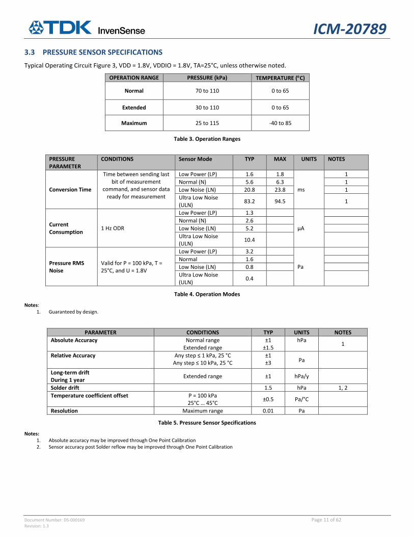
Relative Accuracy Any step ≤ 1 kPa, 25 °C Any step ≤ 10 kPa, 25 °C
±1 ±3 Pa
Long-term drift During 1 year Extended range ±1 hPa/y
Solder drift 1.5 hPa 1, 2 Temperature coefficient offset P = 100 kPa
25°C … 45°C ±0.5 Pa/°C
Resolution Maximum range 0.01 Pa
Table 5. Pressure Sensor Specifications
Notes: 1. Absolute accuracy may be improved through One Point Calibration 2. Sensor accuracy post Solder reflow may be improved through One Point Calibration
ICM-20789
Document Number: DS-000169 Page 12 of 62 Revision: 1.3
Temperature PARAMETER CONDITIONS TYP MAX UNITS NOTES
Absolute Accuracy Extended range ±0.4 °C Repeatability Extended range ±0.1 °C
Resolution Maximum range 0.01 °C Long-term drift Normal range <0.04 °C/y
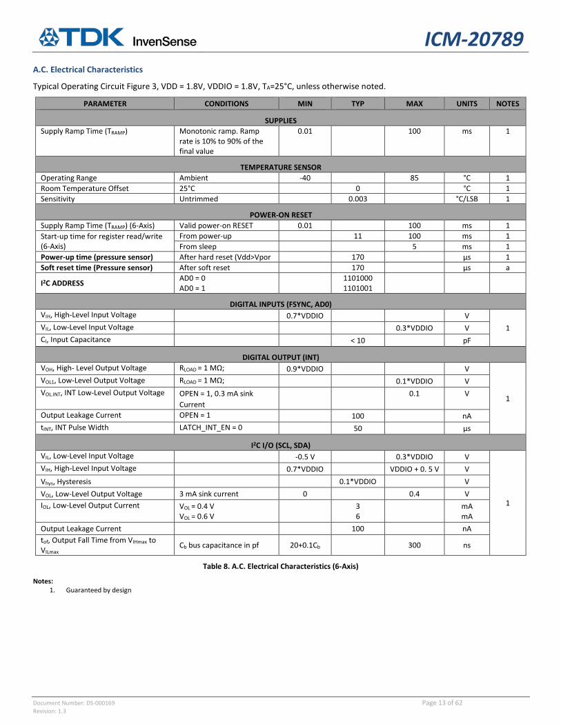
SUPPLIES Supply Ramp Time (TRAMP) Monotonic ramp. Ramp
rate is 10% to 90% of the final value
0.01 100 ms 1
TEMPERATURE SENSOR Operating Range Ambient -40 85 °C 1 Room Temperature Offset 25°C 0 °C 1 Sensitivity Untrimmed 0.003 °C/LSB 1
POWER-ON RESET Supply Ramp Time (TRAMP) (6-Axis) Valid power-on RESET 0.01 100 ms 1 Start-up time for register read/write (6-Axis)
From power-up 11 100 ms 1 From sleep 5 ms 1
Power-up time (pressure sensor) After hard reset (Vdd>Vpor 170 µs 1 Soft reset time (Pressure sensor) After soft reset 170 µs a
I2C ADDRESS AD0 = 0 AD0 = 1 1101000
1101001
DIGITAL INPUTS (FSYNC, AD0) VIH, High-Level Input Voltage 0.7*VDDIO V
1 VIL, Low-Level Input Voltage 0.3*VDDIO V CI, Input Capacitance < 10 pF
DIGITAL OUTPUT (INT) VOH, High- Level Output Voltage RLOAD = 1 MΩ; 0.9*VDDIO V
1
VOL1, Low-Level Output Voltage RLOAD = 1 MΩ; 0.1*VDDIO V VOL.INT, INT Low-Level Output Voltage OPEN = 1, 0.3 mA sink
Current 0.1 V
Output Leakage Current OPEN = 1 100 nA tINT, INT Pulse Width LATCH_INT_EN = 0 50 µs
I2C I/O (SCL, SDA) VIL, Low-Level Input Voltage -0.5 V 0.3*VDDIO V
1
VIH, High-Level Input Voltage 0.7*VDDIO VDDIO + 0. 5 V V Vhys, Hysteresis 0.1*VDDIO V VOL, Low-Level Output Voltage 3 mA sink current 0 0.4 V IOL, Low-Level Output Current VOL = 0.4 V
VOL = 0.6 V 3 6 mA
mA Output Leakage Current 100 nA tof, Output Fall Time from VIHmax to VILmax
Cb bus capacitance in pf 20+0.1Cb 300 ns
Table 8. A.C. Electrical Characteristics (6-Axis)
Notes: 1. Guaranteed by design
ICM-20789
Document Number: DS-000169 Page 14 of 62 Revision: 1.3
PARAMETER SYMBOL CONDITIONS MIN TYP MAX UNITS COMMENTS
Supply voltage VDD 1.71 1.8 1.89 V
Power-up/down level VPOR Static power supply 1.0 1.25 1.5 V
Supply current IDD
Idle state - 1.0 2.5 µA
Measurement - 210 300 µA Current consumption while sensor is measuring.
Average
- 1.3 - µA Current consumption in continuous operation @ 1 Hz ODR in LP Mode
- 5.2 - µA Current consumption in continuous operation @1 Hz ODR in LN Mode
Low level input voltage VIL 0 - 0.3 VDD V
High level input voltage VIH 0.7 VDD - VDD V
Low level output voltage VOL 0 < IOL < 3 mA - - 0.2 VDD V
PARAMETERS CONDITIONS MIN TYP MAX UNITS NOTES I2C TIMING I2C FAST-MODE fSCL, SCL Clock Frequency
400 kHz 1
tHD.STA, (Repeated) START Condition Hold Time
0.6
µs 1 tLOW, SCL Low Period
1.3
µs 1
tHIGH, SCL High Period
0.6
µs 1 tSU.STA, Repeated START Condition Setup Time
0.6
µs 1
tHD.DAT, SDA Data Hold Time
0
µs 1 tSU.DAT, SDA Data Setup Time
100
ns 1
tr, SDA and SCL Rise Time Cb bus cap. from 10 to 400 pF 20+0.1Cb
300 ns 1 tf, SDA and SCL Fall Time Cb bus cap. from 10 to 400 pF 20+0.1Cb
300 ns 1
tSU.STO, STOP Condition Setup Time
0.6
µs 1 tBUF, Bus Free Time Between STOP and START Condition
1.3
µs 1
Cb, Capacitive Load for each Bus Line
< 400
pF 1
ICM-20789
Document Number: DS-000169 Page 15 of 62 Revision: 1.3
PARAMETERS CONDITIONS MIN TYP MAX UNITS NOTES I2C TIMING I2C FAST-MODE tVD.DAT, Data Valid Time
0.9 µs 1
tVD.ACK, Data Valid Acknowledge Time
0.9 µs 1
Table 11. I2C Timing Characteristics
Notes: 1. Based on characterization of 5 parts over temperature and voltage as mounted on evaluation board or in sockets
SDA
SCL
SDA
SCL
70%30%
tf
S
70%30%
tr tSU.DAT
trtHD.DAT70%
30%tHD.STA 1/fSCL
1st clock cycle
70%30%
tLOWtHIGH
tVD.DAT
9th clock cycle
continued below at A
A
Sr P S
70%30%
tSU.STA tHD.STA tVD.ACK tSU.STO
tBUF
70%30%
9th clock cycle
tf
Figure 1. I2C Bus Timing Diagram
ICM-20789
Document Number: DS-000169 Page 16 of 62 Revision: 1.3
3.6 ABSOLUTE MAXIMUM RATINGS Stress above those listed as “Absolute Maximum Ratings” may cause permanent damage to the device. These are stress ratings only and functional operation of the device at these conditions is not implied. Exposure to the absolute maximum ratings conditions for extended periods may affect device reliability.
PARAMETER RATING
Supply Voltage, VDD (for 6-axis MEMS) -0.5V to +4V
Supply Voltage, VDDIO (for Pressure Sensor VDD and I/O) -0.5V to +2.16V
REGOUT -0.5V to 2V
Input Voltage Level (AD0, FSYNC, SCL, SDA) -0.5V to VDD + 0.5V
Acceleration (Any Axis, unpowered) 10,000g for 0.2 ms
Table 13. Absolute Maximum Ratings (pressure sensor)
ICM-20789
Document Number: DS-000169 Page 17 of 62 Revision: 1.3
4 APPLICATIONS INFORMATION 4.1 PIN OUT DIAGRAM AND SIGNAL DESCRIPTION
PIN NUMBER PIN NAME PIN DESCRIPTION 6 PR_DA I2C interface data pin for Pressure Sensor access 7 PR_CL I2C interface clock pin for Pressure Sensor access
8 VDDIO Digital I/O supply voltage 9 AD0/SDO I2C slave address LSB (AD0); SPI serial data output (SDO)
10 REGOUT Regulator filter capacitor connection 11 FSYNC Frame synchronization digital input. Connect to GND if unused. 12 INT Interrupt digital output (totem pole or open-drain)
13 VDD Power supply voltage 18 GND Power supply ground 22 nCS SPI chip select 23 SCL/SCLK I2C serial clock (SCL); SPI serial clock (SCLK)
24 SDA/SDI I2C serial data (SDA); SPI serial data input (SDI) 1, 19, 20, 21 NC No Connect
2, 3, 4, 5, 14, 15, 16, 17 GND/VDD/NC Connect to: GND or VDD or No Connection
Table 14. Signal Descriptions
Note: 1. VDD and VDDIO cannot be shorted if VDD > 1.98V 2. VDD & VDDIO should not violate operating range specifications as mentioned in Section 3.4
ICM-20789
+Z
+X
+Y
7 8 9 10 11 12
PR
_CL
VD
DIO
AD
0/SD
O
RE
GO
UT
FSY
NC
INT
13
18
17
16
15
14
VDD
GND
6
1
2
3
4
5
PR_DA
GND/VDD/NC
NC
24 23 22 21 20 19
NC
NC
NC
nCS
SC
L/SC
LK
SD
A/S
DI
ICM-20789
Top View – LGA Package24-pin, 4mm x 4mm x 1.365mm
Orientation of Axes of Sensitivity and Polarity of Rotation
+Z
+Y
+X
GND/VDD/NC
GND/VDD/NC
GND/VDD/NC
GND/VDD/NC
GND/VDD/NC
GND/VDD/NC
GND/VDD/NC
Figure 2. Pin out Diagram for ICM-20789
ICM-20789
Document Number: DS-000169 Page 18 of 62 Revision: 1.3
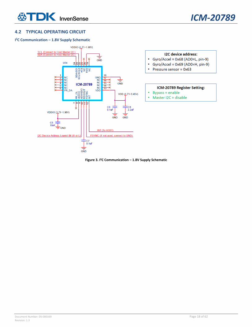
4.2 TYPICAL OPERATING CIRCUIT I2C Communication – 1.8V Supply Schematic
Figure 3. I2C Communication – 1.8V Supply Schematic
ICM-20789
Document Number: DS-000169 Page 19 of 62 Revision: 1.3
I2C Communication MCU Interface at 3V or 1.8V Schematic
Figure 4. I2C Communication MCU Interface at 3V or 1.8V Schematic
ICM-20789
Document Number: DS-000169 Page 20 of 62 Revision: 1.3
SPI Communication for Gyro/Accel; I2C for Pressure Schematic
Figure 5. SPI Communication for Gyro/Accel; I2C for Pressure Schematic
SPI Communication for Gyro/Accel; I2C Pressure; MCU Digital Interface: 1.8V Schematic
Figure 6. SPI Communication for Gyro/Accel; I2C Pressure; MCU Digital Interface: 1.8V Schematic
ICM-20789
Document Number: DS-000169 Page 21 of 62 Revision: 1.3
SPI Communication for Gyro/Accel; I2C for Pressure; MCU Digital Interface: 3.0V Schematic
Figure 7. SPI Communication for Gyro/Accel; I2C for Pressure; MCU Digital Interface: 3.0V Schematic
Note: I2C lines are open drain and pullup resistors (e.g. 10 kΩ) are required.
4.3 BILL OF MATERIALS FOR EXTERNAL COMPONENTS
COMPONENT LABEL SPECIFICATION QUANTITY
REGOUT Capacitor C1 X7R, 0.1 µF ±10% 1
VDD Bypass Capacitors C2 X7R, 0.1 µF ±10% 1
C4 X7R, 2.2 µF ±10% 1
VDDIO Bypass Capacitor C3 X7R, 10 nF ±10% 1
Table 15. Bill of Materials
ICM-20789
Document Number: DS-000169 Page 22 of 62 Revision: 1.3
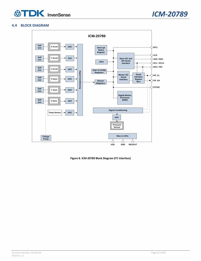
4.4 BLOCK DIAGRAM
ICM-20789
Charge Pump
nCS
AD0 / SDO
SCL / SCLK
SDA / SDI
Temp Sensor ADC
ADCZ Gyro
ADCY Gyro
Digital Motion Processor
(DMP)
FSYNC
Slave I2C and SPI Serial Interface
Master I2C Serial
Interface
Serial Interface Bypass
Mux
PR_CL
PR_DA
INT1Interrupt Status
Register
VDD
Bias & LDOs
GND REGOUT
Z Accel
Y Accel
X Accel ADC
ADC
ADC
ADCX Gyro
Signal Conditioning
FIFO
User & Config Registers
Sensor Registers
Self test
Self test
Self test
Self test
Self test
Self test
PressureSensor
ADC
Signal Conditioning
Figure 8. ICM-20789 Block Diagram (I2C interface)
ICM-20789
Document Number: DS-000169 Page 23 of 62 Revision: 1.3
4.5 OVERVIEW The ICM-20789 is comprised of the following key blocks and functions:
• Three-axis MEMS rate gyroscope sensor with 16-bit ADCs and signal conditioning • Three-axis MEMS accelerometer sensor with 16-bit ADCs and signal conditioning • Digital Motion Processor (DMP) engine • I2C serial communications interfaces • Self-Test • Clocking • Sensor Data Registers • FIFO • Interrupts • Digital-Output Temperature Sensor • Bias and LDOs • Charge Pump • Standard Power Modes • Pressure Sensor
ICM-20789
Document Number: DS-000169 Page 24 of 62 Revision: 1.3
4.6 THREE-AXIS MEMS GYROSCOPE WITH 16-BIT ADCS AND SIGNAL CONDITIONING The ICM-20789 consists of three independent vibratory MEMS rate gyroscopes, which detect rotation about the X-, Y-, and Z- Axes. When the gyros are rotated about any of the sense axes, the Coriolis Effect causes a vibration that is detected by a capacitive pickoff. The resulting signal is amplified, demodulated, and filtered to produce a voltage that is proportional to the angular rate. This voltage is digitized using individual on-chip 16-bit Analog-to-Digital Converters (ADCs) to sample each axis. The full-scale range of the gyro sensors may be digitally programmed to ±250, ±500, ±1000, or ±2000 degrees/sec (dps). The ADC sample rate is programmable from 8,000 samples/sec, to 3.9 samples/sec, and user-selectable low-pass filters enable a wide range of cut-off frequencies.
4.7 THREE-AXIS MEMS ACCELEROMETER WITH 16-BIT ADCS AND SIGNAL CONDITIONING The ICM-20789’s 3-Axis accelerometer uses separate proof masses for each axis. Acceleration along a particular axis induces displacement on the corresponding proof mass, and capacitive sensors detect the displacement differentially. The ICM-20789’s architecture reduces the accelerometers’ susceptibility to fabrication variations as well as to thermal drift. When the device is placed on a flat surface, it will measure 0g on the X- and Y-axes and +1g on the Z-axis. The accelerometers’ scale factor is calibrated at the factory and is nominally independent of supply voltage. Each sensor has a dedicated sigma-delta ADC for providing digital outputs. The full-scale range of the digital output can be adjusted to ±2g, ±4g, ±8g, or ±16g.
4.8 DIGITAL MOTION PROCESSOR The embedded Digital Motion Processor (DMP) offloads computation of motion processing algorithms from the host processor. The DMP acquires data from the accelerometer and gyroscope, processes the data, and the results can be read from the FIFO. The DMP has access to one of the external pins, which can be used for generating interrupts. The purpose of the DMP is to offload both timing requirements and processing power from the host processor. Typically, motion processing algorithms should be run at a high rate, often around 200 Hz, in order to provide accurate results with low latency. This is required even if the application updates at a much lower rate; for example, a low power user interface may update as slowly as 5 Hz, but the motion processing should still run at 200 Hz. The DMP can be used to minimize power, simplify timing, simplify the software architecture, and save valuable MIPS on the host processor for use in applications. DMP operation is possible in low-power gyroscope and low-power accelerometer modes.
4.9 PRESSURE SENSOR The pressure sensor is a capacitive pressure sensor, and has a membrane over a sealed cavity at a reference pressure. External pressure changes relative to the sealed cavity pressure cause the membrane to deflect. The membrane and the floor of the cavity form a capacitor where the capacitance changes in response to changes in external pressure. The capacitance measurement is converted to a voltage proportional to the external pressure by the on-chip electronics. An external algorithm is used to compensate for temperature effects on the pressure accuracy.
4.10 I2C SERIAL COMMUNICATIONS INTERFACE The ICM-20789 communicates to a system processor using a I2C serial interface. The ICM-20789 always acts as a slave when communicating to the system processor. The LSB of the I2C slave address is set by pin 9 (AD0).
ICM-20789
Document Number: DS-000169 Page 25 of 62 Revision: 1.3
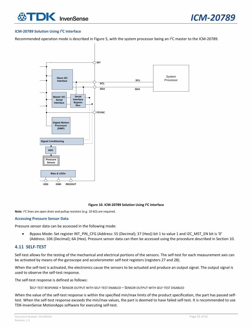
ICM-20789 Solution Using I2C Interface
Recommended operation mode is described in Figure 5, with the system processor being an I2C master to the ICM-20789.
-20948
SCL
SDA
Digital Motion Processor
(DMP)
FSYNC
Slave I2C Interface
Master I2C Serial
Interface
Serial Interface Bypass
Mux
INT
VDD
Bias & LDOs
GND REGOUT
PressureSensor
ADC
Signal Conditioning
SystemProcessorSCL
SDA
Figure 10. ICM-20789 Solution Using I2C Interface
Note: I2C lines are open drain and pullup resistors (e.g. 10 kΩ) are required.
Accessing Pressure Sensor Data
Pressure sensor data can be accessed in the following mode:
• Bypass Mode: Set register INT_PIN_CFG (Address: 55 (Decimal); 37 (Hex)) bit 1 to value 1 and I2C_MST_EN bit is ‘0’ (Address: 106 (Decimal); 6A (Hex). Pressure sensor data can then be accessed using the procedure described in Section 10.
4.11 SELF-TEST Self-test allows for the testing of the mechanical and electrical portions of the sensors. The self-test for each measurement axis can be activated by means of the gyroscope and accelerometer self-test registers (registers 27 and 28).
When the self-test is activated, the electronics cause the sensors to be actuated and produce an output signal. The output signal is used to observe the self-test response.
The self-test response is defined as follows:
SELF-TEST RESPONSE = SENSOR OUTPUT WITH SELF-TEST ENABLED – SENSOR OUTPUT WITH SELF-TEST DISABLED
When the value of the self-test response is within the specified min/max limits of the product specification, the part has passed self-test. When the self-test response exceeds the min/max values, the part is deemed to have failed self-test. It is recommended to use TDK-InvenSense MotionApps software for executing self-test.
ICM-20789
Document Number: DS-000169 Page 26 of 62 Revision: 1.3
4.12 CLOCKING The ICM-20789 has a flexible clocking scheme, allowing a variety of internal clock sources to be used for the internal synchronous circuitry. This synchronous circuitry includes the signal conditioning and ADCs, the DMP, and various control circuits and registers. An on-chip PLL provides flexibility in the allowable inputs for generating this clock.
Allowable internal sources for generating the internal clock are:
a) An internal relaxation oscillator b) Auto-select between internal relaxation oscillator and gyroscope MEMS oscillator to use the best available source
The only setting supporting specified performance in all modes is option b). It is recommended that option b) be used.
4.13 SENSOR DATA REGISTERS The sensor data registers contain the latest gyroscope, accelerometer, and temperature measurement data. They are read-only registers, and are accessed via the serial interface. Data from these registers may be read anytime.
4.14 FIFO The ICM-20789 contains a 4 kB FIFO register that is accessible via the Serial Interface. The FIFO configuration register determines which data is written into the FIFO. Possible choices include gyro data, accelerometer data, temperature readings, and FSYNC input. A FIFO counter keeps track of how many bytes of valid data are contained in the FIFO. The FIFO register supports burst reads. The interrupt function may be used to determine when new data is available.
The ICM-20789 allows FIFO read in low-power accelerometer mode.
4.15 INTERRUPTS Interrupt functionality is configured via the Interrupt Configuration register. Items that are configurable include the INT pin configuration, the interrupt latching and clearing method, and triggers for the interrupt. Items that can trigger an interrupt are (1) Clock generator locked to new reference oscillator (used when switching clock sources); (2) new data is available to be read (from the FIFO and Data registers); (3) accelerometer event interrupts; (4) DMP; (5) FIFO overflow. The interrupt status can be read from the Interrupt Status register.
4.16 DIGITAL-OUTPUT TEMPERATURE SENSOR An on-chip temperature sensor and ADC are used to measure the 6-axis motion die temperature. Another on-chip temperature sensor is present in the pressure sensor die. The readings from the ADC can be read from the FIFO or the Sensor Data registers.
4.17 BIAS AND LDOS The bias and LDO section generates the internal supply and the reference voltages and currents required by the ICM-20789. Its two inputs are an unregulated VDD and a VDDIO logic reference supply voltage. The LDO output is bypassed by a capacitor at REGOUT. For further details on the capacitor, please refer to the Bill of Materials for External Components.
4.18 CHARGE PUMP An on-chip charge pump generates the high voltage required for the MEMS oscillator.
ICM-20789
Document Number: DS-000169 Page 27 of 62 Revision: 1.3
4.19 STANDARD POWER MODES – UPDATE THE POWER MODES The following table lists the user-accessible power modes for ICM-20789.
MODE NAME GYRO ACCEL DMP PRESSURE 1 Sleep Mode Off Off Off Off 2 Standby Mode Drive On Off Off Off 3 Accelerometer Low-Power Mode Off Duty-Cycled On or Off On or Off 4 Accelerometer Low-Noise Mode Off On On or Off On or Off 5 Gyroscope Low-Power Mode Duty-Cycled Off On or Off On or Off 6 Gyroscope Low-Noise Mode On Off On or Off On or Off 7 6-Axis Low-Noise Mode On On On or Off On or Off 8 6-Axis Low-Power Mode Duty-Cycled On On or Off On or Off 9 Pressure sensor Low Noise Mode On On On or Off On
10 Pressure Sensor Low Power Mode Duty-Cycled On On or Off On
Table 16. Standard Power Modes for ICM-20789
ICM-20789
Document Number: DS-000169 Page 28 of 62 Revision: 1.3
5 PROGRAMMABLE INTERRUPTS The ICM-20789 has a programmable interrupt system which can generate an interrupt signal on the INT pin. Status flags indicate the source of an interrupt. Interrupt sources may be enabled and disabled individually.
INTERRUPT NAME MODULE
Motion Detection Motion
FIFO Overflow FIFO
Data Ready Sensor Registers
DMP DMP
Table 17. Table of Interrupt Sources
5.1 PER AXIS WAKE-ON-MOTION INTERRUPT The ICM-20789 provides motion detection capability. A qualifying motion sample is one where the high passed sample from any axis has an absolute value exceeding a user-programmable threshold. The following steps explain how to configure the Wake-on-Motion Interrupt.
Step 1: Ensure that Accelerometer is running
• In PWR_MGMT_1 register (0x6B) set CYCLE = 0, SLEEP = 0, and GYRO_STANDBY = 0 • In PWR_MGMT_2 register (0x6C) set DISABLE_XA = DISABLE_YA = DISABLE_ZA = 0, and DISABLE_XG = DISABLE_YG =
DISABLE_ZG = 1
Step 2: Accelerometer Configuration
1. In ACCEL_CONFIG2 register (0x1D) set ACCEL_FCHOICE_B = 0 and A_DLPF_CFG [2:0] = 1 (b001)
Step 3: Enable Motion Interrupt
2. In INT_ENABLE register (0x38) set WOM_X_INT_EN = WOM_Y_INT_EN = WOM_Z_INT_EN = 1 to enable motion interrupt per axis.
Step 4: Set Motion Threshold
3. Set the motion threshold in ACCEL_WOM_X_THR (0x20), ACCEL_WOM_Y_THR (0x21), ACCEL_WOM_Z_THR (0x22)
Document Number: DS-000169 Page 29 of 62 Revision: 1.3
6 DIGITAL INTERFACE 6.1 I2C SERIAL INTERFACE The internal registers and memory of the ICM-20789 can be accessed using either I2C at 400 kHz.
PIN NUMBER PIN NAME PIN DESCRIPTION
9 AD0 I2C Slave Address LSB (AD0)
23 SCL I2C serial clock (SCL)
24 SDA I2C serial data (SDA)
Table 18. Serial Interface
6.2 I2C INTERFACE I2C is a two-wire interface comprised of the signals serial data (SDA) and serial clock (SCL). In general, the lines are open-drain and bi-directional. In a generalized I2C interface implementation, attached devices can be a master or a slave. The master device puts the slave address on the bus, and the slave device with the matching address acknowledges the master.
The ICM-20789 always operates as a slave device when communicating to the system processor, which thus acts as the master. SDA and SCL lines typically need pull-up resistors to VDDIO. The maximum bus speed is 400 kHz.
The slave address of the ICM-20789 is b110100X which is 7 bits long. The LSB bit of the 7-bit address is determined by the logic level on pin AD0. This allows two ICM-20789s to be connected to the same I2C bus. When used in this configuration, the address of one of the devices should be b1101000 (pin AD0 is logic low) and the address of the other should be b1101001 (pin AD0 is logic high).
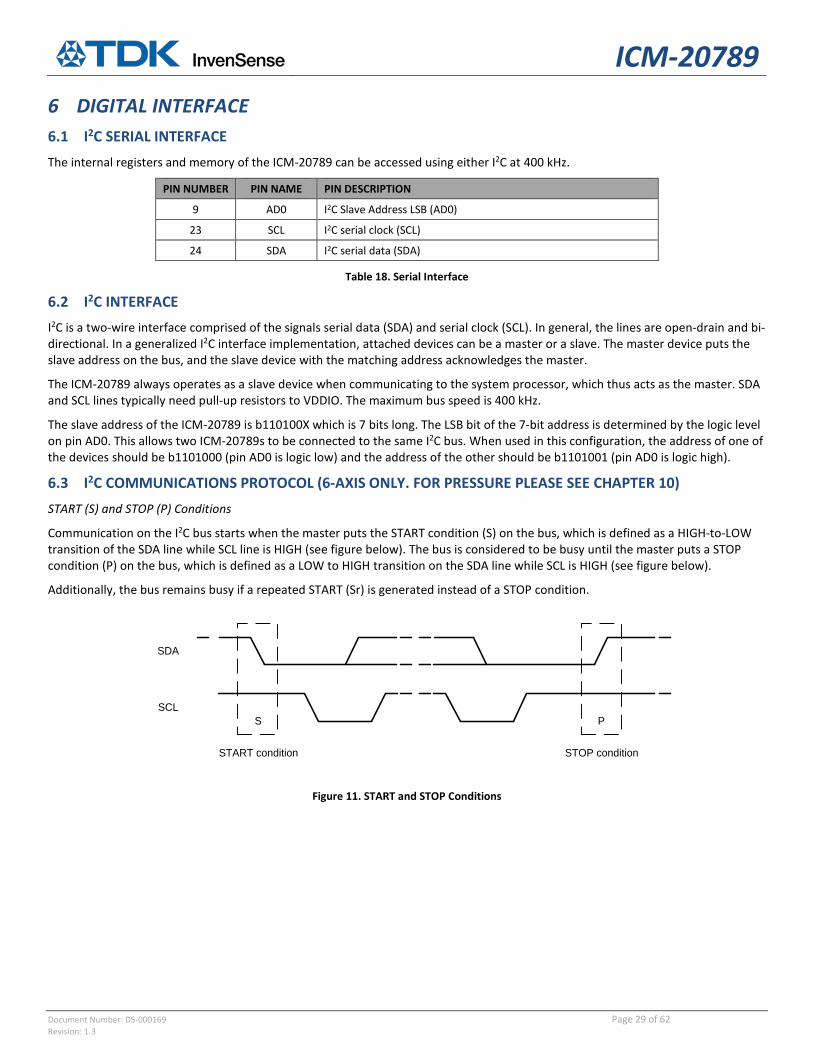
6.3 I2C COMMUNICATIONS PROTOCOL (6-AXIS ONLY. FOR PRESSURE PLEASE SEE CHAPTER 10) START (S) and STOP (P) Conditions
Communication on the I2C bus starts when the master puts the START condition (S) on the bus, which is defined as a HIGH-to-LOW transition of the SDA line while SCL line is HIGH (see figure below). The bus is considered to be busy until the master puts a STOP condition (P) on the bus, which is defined as a LOW to HIGH transition on the SDA line while SCL is HIGH (see figure below).
Additionally, the bus remains busy if a repeated START (Sr) is generated instead of a STOP condition.
SDA
SCLS
START condition STOP condition
P
Figure 11. START and STOP Conditions
ICM-20789
Document Number: DS-000169 Page 30 of 62 Revision: 1.3
Data Format / Acknowledge
I2C data bytes are defined to be 8 bits long. There is no restriction to the number of bytes transmitted per data transfer. Each byte transferred must be followed by an acknowledge (ACK) signal. The clock for the acknowledge signal is generated by the master, while the receiver generates the actual acknowledge signal by pulling down SDA and holding it low during the HIGH portion of the acknowledge clock pulse.
If a slave is busy and cannot transmit or receive another byte of data until some other task has been performed, it can hold SCL LOW, thus forcing the master into a wait state. Normal data transfer resumes when the slave is ready, and releases the clock line (refer to the following figure).
DATA OUTPUT BY TRANSMITTER (SDA)
DATA OUTPUT BY RECEIVER (SDA)
SCL FROM MASTER
START condition
clock pulse for acknowledgement
acknowledge
not acknowledge
1 2 8 9
Figure 12. Acknowledge on the I2C Bus
Communications
After beginning communications with the START condition (S), the master sends a 7-bit slave address followed by an 8th bit, the read/write bit. The read/write bit indicates whether the master is receiving data from or is writing to the slave device. Then, the master releases the SDA line and waits for the acknowledge signal (ACK) from the slave device. Each byte transferred must be followed by an acknowledge bit. To acknowledge, the slave device pulls the SDA line LOW and keeps it LOW for the high period of the SCL line. Data transmission is always terminated by the master with a STOP condition (P), thus freeing the communications line. However, the master can generate a repeated START condition (Sr), and address another slave without first generating a STOP condition (P). A LOW to HIGH transition on the SDA line while SCL is HIGH defines the stop condition. All SDA changes should take place when SCL is low, with the exception of start and stop conditions.
SDA
START condition
SCL
ADDRESS R/W ACK DATA ACK DATA ACK STOP condition
S P
1 – 7 8 9 1 – 7 8 9 1 – 7 8 9
Figure 13. Complete I2C Data Transfer
ICM-20789
Document Number: DS-000169 Page 31 of 62 Revision: 1.3
To write the internal ICM-20789 registers, the master transmits the start condition (S), followed by the I2C address and the write bit (0). At the 9th clock cycle (when the clock is high), the ICM-20789 acknowledges the transfer. Then the master puts the register address (RA) on the bus. After the ICM-20789 acknowledges the reception of the register address, the master puts the register data onto the bus. This is followed by the ACK signal, and data transfer may be concluded by the stop condition (P). To write multiple bytes after the last ACK signal, the master can continue outputting data rather than transmitting a stop signal. In this case, the ICM-20789 automatically increments the register address and loads the data to the appropriate register. The following figures show single and two-byte write sequences.
Single-Byte Write Sequence
Burst Write Sequence
To read the internal ICM-20789 registers, the master sends a start condition, followed by the I2C address and a write bit, and then the register address that is going to be read. Upon receiving the ACK signal from the ICM-20789, the master transmits a start signal followed by the slave address and read bit. As a result, the ICM-20789 sends an ACK signal and the data. The communication ends with a not acknowledge (NACK) signal and a stop bit from master. The NACK condition is defined such that the SDA line remains high at the 9th clock cycle. The following figures show single and two-byte read sequences.
Single-Byte Read Sequence
Burst Read Sequence
6.4 I2C TERMS
SIGNAL DESCRIPTION S Start Condition: SDA goes from high to low while SCL is high
AD Slave I2C address W Write bit (0) R Read bit (1)
ACK Acknowledge: SDA line is low while the SCL line is high at the 9th clock cycle NACK Not-Acknowledge: SDA line stays high at the 9th clock cycle
RA ICM-20789 internal register address DATA Transmit or received data
P Stop condition: SDA going from low to high while SCL is high
Table 19. I2C Term SPI Interface
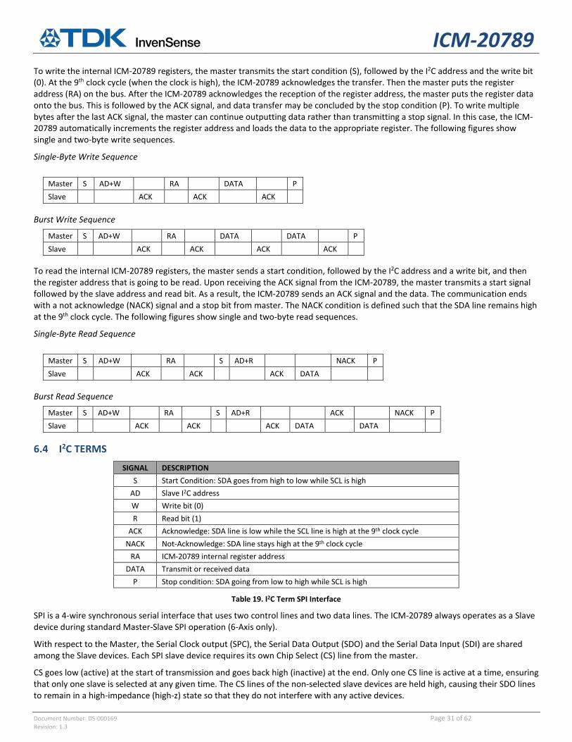
SPI is a 4-wire synchronous serial interface that uses two control lines and two data lines. The ICM-20789 always operates as a Slave device during standard Master-Slave SPI operation (6-Axis only).
With respect to the Master, the Serial Clock output (SPC), the Serial Data Output (SDO) and the Serial Data Input (SDI) are shared among the Slave devices. Each SPI slave device requires its own Chip Select (CS) line from the master.
CS goes low (active) at the start of transmission and goes back high (inactive) at the end. Only one CS line is active at a time, ensuring that only one slave is selected at any given time. The CS lines of the non-selected slave devices are held high, causing their SDO lines to remain in a high-impedance (high-z) state so that they do not interfere with any active devices.
Master S AD+W RA DATA P Slave ACK ACK ACK
Master S AD+W RA DATA DATA P Slave ACK ACK ACK ACK
Master S AD+W RA S AD+R NACK P Slave ACK ACK ACK DATA
Master S AD+W RA S AD+R ACK NACK P Slave ACK ACK ACK DATA DATA
ICM-20789
Document Number: DS-000169 Page 32 of 62 Revision: 1.3
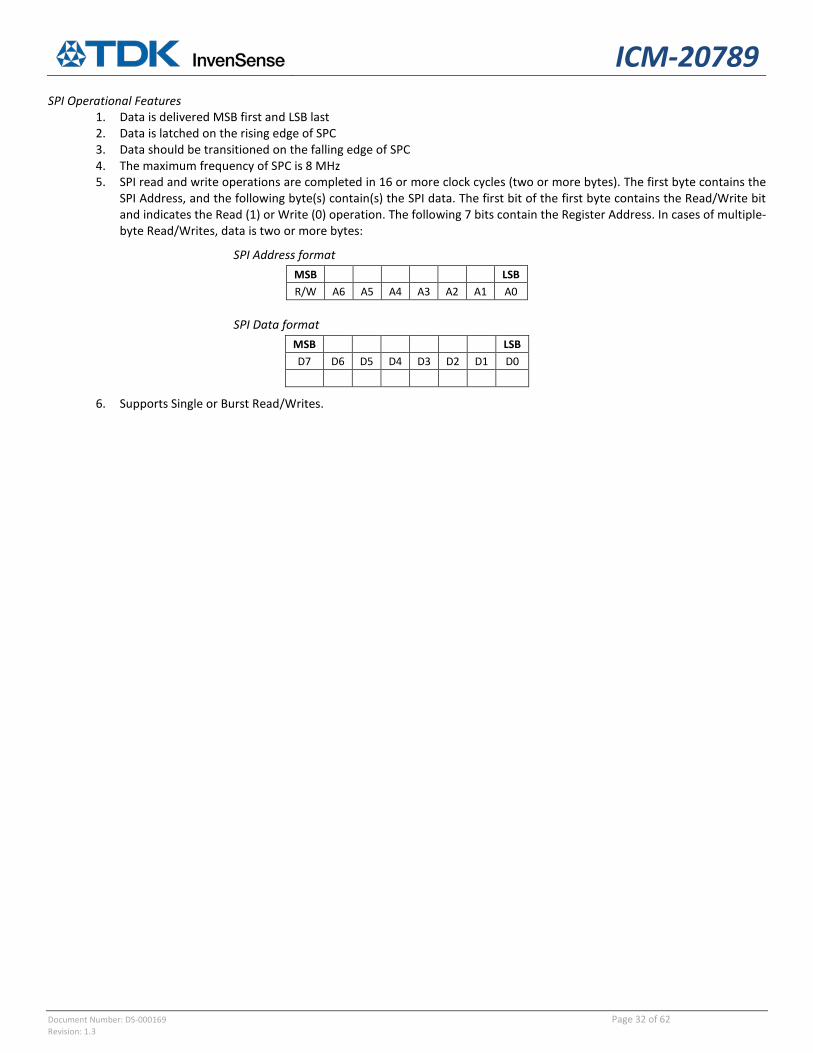
SPI Operational Features 1. Data is delivered MSB first and LSB last 2. Data is latched on the rising edge of SPC 3. Data should be transitioned on the falling edge of SPC 4. The maximum frequency of SPC is 8 MHz 5. SPI read and write operations are completed in 16 or more clock cycles (two or more bytes). The first byte contains the
SPI Address, and the following byte(s) contain(s) the SPI data. The first bit of the first byte contains the Read/Write bit and indicates the Read (1) or Write (0) operation. The following 7 bits contain the Register Address. In cases of multiple-byte Read/Writes, data is two or more bytes:
Document Number: DS-000169 Page 33 of 62 Revision: 1.3
7 SERIAL INTERFACE CONSIDERATIONS 7.1 ICM-20789 SUPPORTED INTERFACES The ICM-20789 supports I2C communications on its serial interface. The ICM-20789’s I/O logic levels are set to be VDDIO.
The figure below depicts a sample circuit of ICM-20789. It shows the relevant logic levels and voltage connections.
ICM-20789
VDD
System Processor IO
SYSTEM BUS
VDDIO
VDDIO
VDD
VDDIO
SCL
SDA
INT
SYNC
VDDIO
AD0
(0V - VDDIO)
(0V - VDDIO)(0V - VDDIO)
(0V - VDDIO)
(0V, VDDIO)
VDD_IO
(0V - VDDIO)
Figure 14. I/O Levels and Connections
ICM-20789
Document Number: DS-000169 Page 34 of 62 Revision: 1.3
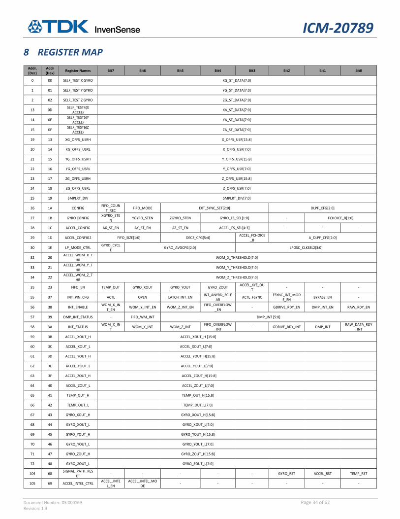
Note: Register Names ending in _H and _L contain the high and low bytes, respectively, of an internal register value.
In the detailed register tables that follow, register names are in capital letters, while register values are in capital letters and italicized. For example, the ACCEL_XOUT_H register (Register 59) contains the 8 most significant bits, ACCEL_XOUT[15:8], of the 16-bit X-Axis accelerometer measurement, ACCEL_XOUT.
The reset value is 0x00 for all registers other than the registers below, also the self-test registers contain pre-programmed values and will not be 0x00 after reset.
• Register 107 (0x40) Power Management 1 • Register 117 (0x03) WHO_AM_I for ICM-20789
ICM-20789
Document Number: DS-000169 Page 36 of 62 Revision: 1.3
9 REGISTER DESCRIPTIONS This section describes the function and contents of each register within the ICM-20789.
Note: The device will come up in sleep mode upon power-up.
9.1 REGISTERS DESCRIPTIONS Reset values are “0” for all registers, unless otherwise specified
9.2 REGISTERS 0 TO 2 – SELF-TEST REGISTERS Register Name: SELF_TEST X GYRO, SELF_TEST Y GYRO, SELF_TEST Z GYRO Type: USR/CFG Register Address: 0, 1, 2 (Decimal); 00, 01, 02 (Hex)
REGISTER BIT NAME FUNCTION
SELF_TEST X GYRO [7:0] XG_ST_DATA The value in this register indicates the self-test output generated during manufacturing tests. This value is to be used to check against subsequent self-test outputs performed by the end user.
SELF_TEST Y GYRO [7:0] YG_ST_DATA The value in this register indicates the self-test output generated during manufacturing tests. This value is to be used to check against subsequent self-test outputs performed by the end user.
SELF_TEST Z GYRO [7:0] ZG_ST_DATA The value in this register indicates the self-test output generated during manufacturing tests. This value is to be used to check against subsequent self-test outputs performed by the end user.
REGISTER BIT NAME FUNCTION SELF_TEST4(X ACCEL) [7:0] XA_ST_DATA[7:0] Contains self-test data for the X Accelerometer SELF_TEST5(Y ACCEL) [7:0] YA_ST_DATA[7:0] Contains self-test data for the Y Accelerometer SELF_TEST6(Z ACCEL) [7:0] ZA_ST_DATA[7:0] Contains self-test data for the Z Accelerometer
[7:0] X_OFFS_USR[15:8] Bits 15 to 8 of the 16-bit offset of X gyroscope (2’s complement). This register is used to remove DC bias from the sensor output. The value in this register is added to the gyroscope sensor value before going into the sensor register.
Bits 7 to 0 of the 16-bit offset of X gyroscope (2’s complement). This register is used to remove DC bias from the sensor output. The value in this register is added to the gyroscope sensor value before going into the sensor register.
ICM-20789
Document Number: DS-000169 Page 37 of 62 Revision: 1.3
Bits 15 to 8 of the 16-bit offset of Y gyroscope (2’s complement). This register is used to remove DC bias from the sensor output. The value in this register is added to the gyroscope sensor value before going into the sensor register.
[7:0] Y_OFFS_USR[7:0] Bits 7 to 0 of the 16-bit offset of Y gyroscope (2’s complement). This register is used to remove DC bias from the sensor output. The value in this register is added to the gyroscope sensor value before going into the sensor register.
[7:0] Z_OFFS_USR[15:8] Bits 15 to 8 of the 16-bit offset of Z gyroscope (2’s complement). This register is used to remove DC bias from the sensor output. The value in this register is added to the gyroscope sensor value before going into the sensor register.
[7:0] Z_OFFS_USR[7:0] Bits 7 to 0 of the 16-bit offset of Z gyroscope (2’s complement). This register is used to remove DC bias from the sensor output. The value in this register is added to the gyroscope sensor value before going into the sensor register.
Divides the internal sample rate (see register CONFIG (0x1A)) to generate the sample rate that controls sensor data output rate, FIFO sample rate. Note: This register is only effective when FCHOICE_B register bits are 2’b00, and (0 < DLPF_CFG < 7). This is the update rate of the sensor register: SAMPLE_RATE = INTERNAL_SAMPLE_RATE / (1 + SMPLRT_DIV) Where INTERNAL_SAMPLE_RATE = 1 kHz
ICM-20789
Document Number: DS-000169 Page 38 of 62 Revision: 1.3
BIT NAME FUNCTION [7] FIFO_COUNT_REC Always set to 0.
[6] FIFO_MODE When set to ‘1’, when the fifo is full, additional writes will not be written to fifo. When set to ‘0’, when the fifo is full, additional writes will be written to the fifo, replacing the oldest data.
[5:3] EXT_SYNC_SET[2:0]
Enables the FSYNC pin data to be sampled. EXT_SYNC_SET FSYNC bit location 0 function disabled 1 TEMP_OUT_L[0] 2 GYRO_XOUT_L[0] 3 GYRO_YOUT_L[0] 4 GYRO_ZOUT_L[0] 5 ACCEL_XOUT_L[0] 6 ACCEL_YOUT_L[0] 7 ACCEL_ZOUT_L[0]
[2:0] DLPF_CFG[2:0] For the DLPF to be used, FCHOICE_B[1:0] is 2’b00. See the table below.
The DLPF is configured by DLPF_CFG, when FCHOICE_B [1:0] = 2b’00. The gyroscope and temperature sensor are filtered according to the value of DLPF_CFG and FCHOICE_B as shown in the table below.
Fifo size control: 0=512bytes, 1=1 KB, 2=2 KB, 3=4 KB NOTE: After the fifo size has been changed, the fifo should be reset.
[5:4] DEC2_CFG
Controls the number of samples averaged in the accel decimator 2: 0 = average 4 samples 1 = average 8 samples 2 = average 16 samples 3 = average 32 samples
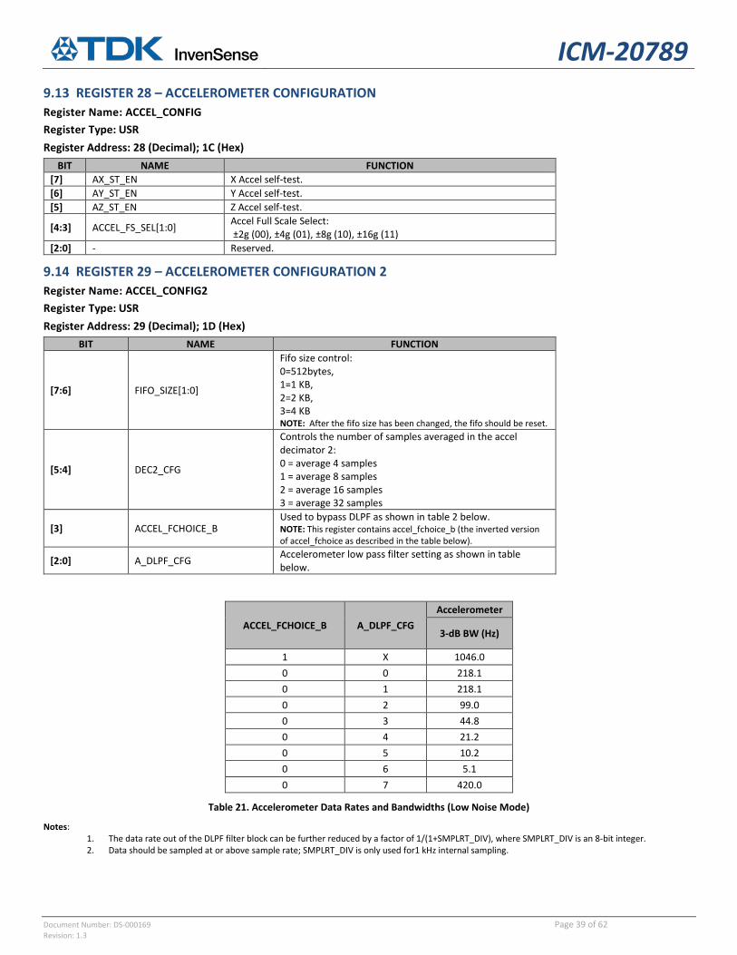
[3] ACCEL_FCHOICE_B Used to bypass DLPF as shown in table 2 below. NOTE: This register contains accel_fchoice_b (the inverted version of accel_fchoice as described in the table below).
[2:0] A_DLPF_CFG Accelerometer low pass filter setting as shown in table below.
Table 21. Accelerometer Data Rates and Bandwidths (Low Noise Mode)
Notes: 1. The data rate out of the DLPF filter block can be further reduced by a factor of 1/(1+SMPLRT_DIV), where SMPLRT_DIV is an 8-bit integer. 2. Data should be sampled at or above sample rate; SMPLRT_DIV is only used for1 kHz internal sampling.
ICM-20789
Document Number: DS-000169 Page 40 of 62 Revision: 1.3
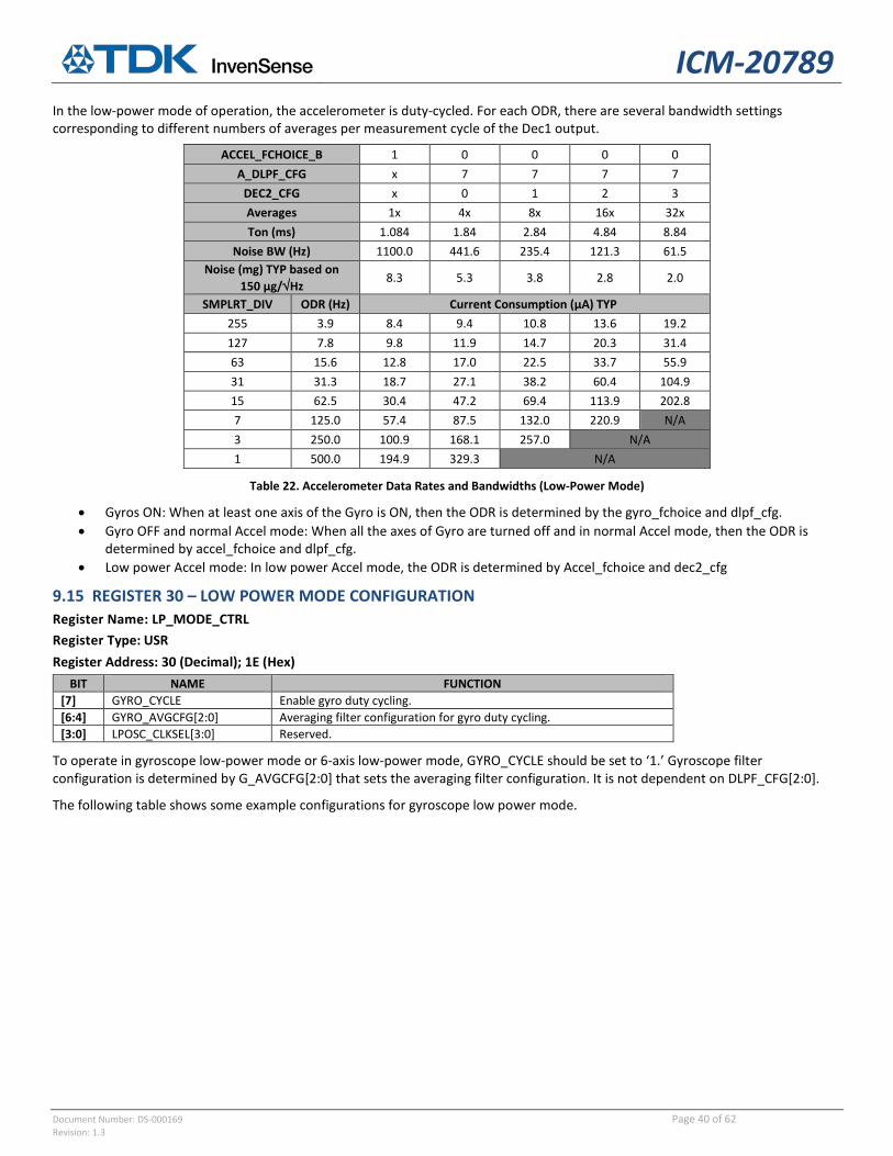
In the low-power mode of operation, the accelerometer is duty-cycled. For each ODR, there are several bandwidth settings corresponding to different numbers of averages per measurement cycle of the Dec1 output.
ACCEL_FCHOICE_B 1 0 0 0 0 A_DLPF_CFG x 7 7 7 7
DEC2_CFG x 0 1 2 3 Averages 1x 4x 8x 16x 32x Ton (ms) 1.084 1.84 2.84 4.84 8.84
Noise BW (Hz) 1100.0 441.6 235.4 121.3 61.5 Noise (mg) TYP based on
Table 22. Accelerometer Data Rates and Bandwidths (Low-Power Mode)
• Gyros ON: When at least one axis of the Gyro is ON, then the ODR is determined by the gyro_fchoice and dlpf_cfg. • Gyro OFF and normal Accel mode: When all the axes of Gyro are turned off and in normal Accel mode, then the ODR is
determined by accel_fchoice and dlpf_cfg. • Low power Accel mode: In low power Accel mode, the ODR is determined by Accel_fchoice and dec2_cfg
9.15 REGISTER 30 – LOW POWER MODE CONFIGURATION Register Name: LP_MODE_CTRL Register Type: USR Register Address: 30 (Decimal); 1E (Hex)
BIT NAME FUNCTION [7] GYRO_CYCLE Enable gyro duty cycling. [6:4] GYRO_AVGCFG[2:0] Averaging filter configuration for gyro duty cycling. [3:0] LPOSC_CLKSEL[3:0] Reserved.
To operate in gyroscope low-power mode or 6-axis low-power mode, GYRO_CYCLE should be set to ‘1.’ Gyroscope filter configuration is determined by G_AVGCFG[2:0] that sets the averaging filter configuration. It is not dependent on DLPF_CFG[2:0].
The following table shows some example configurations for gyroscope low power mode.
ICM-20789
Document Number: DS-000169 Page 41 of 62 Revision: 1.3
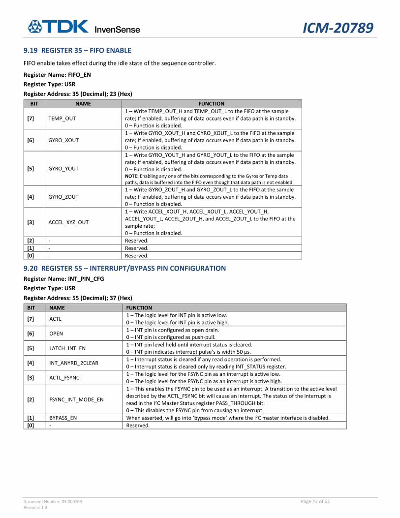
[7] TEMP_OUT 1 – Write TEMP_OUT_H and TEMP_OUT_L to the FIFO at the sample rate; If enabled, buffering of data occurs even if data path is in standby. 0 – Function is disabled.
[6] GYRO_XOUT 1 – Write GYRO_XOUT_H and GYRO_XOUT_L to the FIFO at the sample rate; If enabled, buffering of data occurs even if data path is in standby. 0 – Function is disabled.
[5] GYRO_YOUT
1 – Write GYRO_YOUT_H and GYRO_YOUT_L to the FIFO at the sample rate; If enabled, buffering of data occurs even if data path is in standby. 0 – Function is disabled. NOTE: Enabling any one of the bits corresponding to the Gyros or Temp data paths, data is buffered into the FIFO even though that data path is not enabled.
[4] GYRO_ZOUT 1 – Write GYRO_ZOUT_H and GYRO_ZOUT_L to the FIFO at the sample rate; If enabled, buffering of data occurs even if data path is in standby. 0 – Function is disabled.
[3] ACCEL_XYZ_OUT
1 – Write ACCEL_XOUT_H, ACCEL_XOUT_L, ACCEL_YOUT_H, ACCEL_YOUT_L, ACCEL_ZOUT_H, and ACCEL_ZOUT_L to the FIFO at the sample rate; 0 – Function is disabled.
[7] ACTL 1 – The logic level for INT pin is active low. 0 – The logic level for INT pin is active high.
[6] OPEN 1 – INT pin is configured as open drain. 0 – INT pin is configured as push-pull.
[5] LATCH_INT_EN 1 – INT pin level held until interrupt status is cleared. 0 – INT pin indicates interrupt pulse’s is width 50 µs.
[4] INT_ANYRD_2CLEAR 1 – Interrupt status is cleared if any read operation is performed. 0 – Interrupt status is cleared only by reading INT_STATUS register.
[3] ACTL_FSYNC 1 – The logic level for the FSYNC pin as an interrupt is active low. 0 – The logic level for the FSYNC pin as an interrupt is active high.
[2] FSYNC_INT_MODE_EN
1 – This enables the FSYNC pin to be used as an interrupt. A transition to the active level described by the ACTL_FSYNC bit will cause an interrupt. The status of the interrupt is read in the I2C Master Status register PASS_THROUGH bit. 0 – This disables the FSYNC pin from causing an interrupt.
[1] BYPASS_EN When asserted, will go into ‘bypass mode’ where the I2C master interface is disabled. [0] - Reserved.
ICM-20789
Document Number: DS-000169 Page 43 of 62 Revision: 1.3
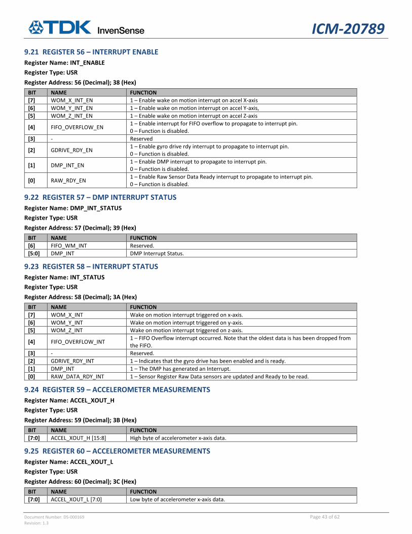
BIT NAME FUNCTION [7] WOM_X_INT_EN 1 – Enable wake on motion interrupt on accel X-axis [6] WOM_Y_INT_EN 1 – Enable wake on motion interrupt on accel Y-axis, [5] WOM_Z_INT_EN 1 – Enable wake on motion interrupt on accel Z-axis
[4] FIFO_OVERFLOW_EN 1 – Enable interrupt for FIFO overflow to propagate to interrupt pin. 0 – Function is disabled.
[3] - Reserved
[2] GDRIVE_RDY_EN 1 – Enable gyro drive rdy interrupt to propagate to interrupt pin. 0 – Function is disabled.
[1] DMP_INT_EN 1 – Enable DMP interrupt to propagate to interrupt pin. 0 – Function is disabled.
[0] RAW_RDY_EN 1 – Enable Raw Sensor Data Ready interrupt to propagate to interrupt pin. 0 – Function is disabled.
BIT NAME FUNCTION [7] WOM_X_INT Wake on motion interrupt triggered on x-axis. [6] WOM_Y_INT Wake on motion interrupt triggered on y-axis. [5] WOM_Z_INT Wake on motion interrupt triggered on z-axis.
[4] FIFO_OVERFLOW_INT 1 – FIFO Overflow interrupt occurred. Note that the oldest data is has been dropped from the FIFO.
[3] - Reserved. [2] GDRIVE_RDY_INT 1 – Indicates that the gyro drive has been enabled and is ready. [1] DMP_INT 1 – The DMP has generated an Interrupt. [0] RAW_DATA_RDY_INT 1 – Sensor Register Raw Data sensors are updated and Ready to be read.
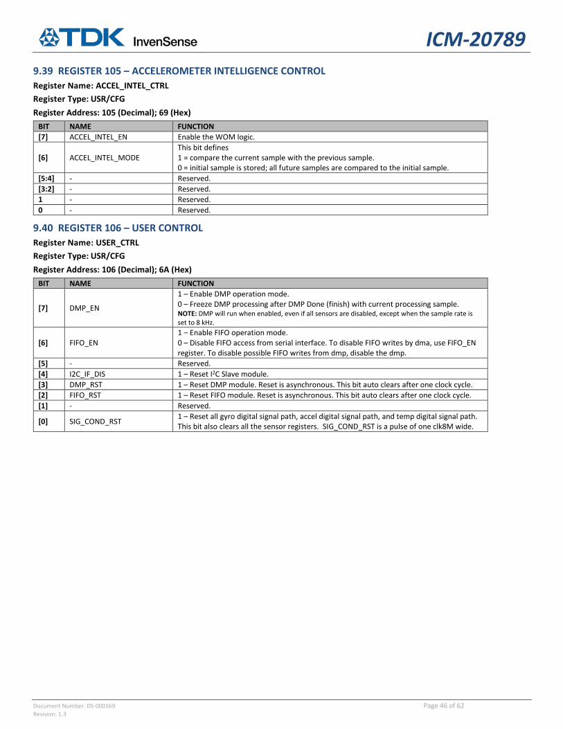
BIT NAME FUNCTION [7] ACCEL_INTEL_EN Enable the WOM logic.
[6] ACCEL_INTEL_MODE This bit defines 1 = compare the current sample with the previous sample. 0 = initial sample is stored; all future samples are compared to the initial sample.
9.40 REGISTER 106 – USER CONTROL Register Name: USER_CTRL Register Type: USR/CFG Register Address: 106 (Decimal); 6A (Hex)
BIT NAME FUNCTION
[7] DMP_EN
1 – Enable DMP operation mode. 0 – Freeze DMP processing after DMP Done (finish) with current processing sample. NOTE: DMP will run when enabled, even if all sensors are disabled, except when the sample rate is set to 8 kHz.
[6] FIFO_EN 1 – Enable FIFO operation mode. 0 – Disable FIFO access from serial interface. To disable FIFO writes by dma, use FIFO_EN register. To disable possible FIFO writes from dmp, disable the dmp.
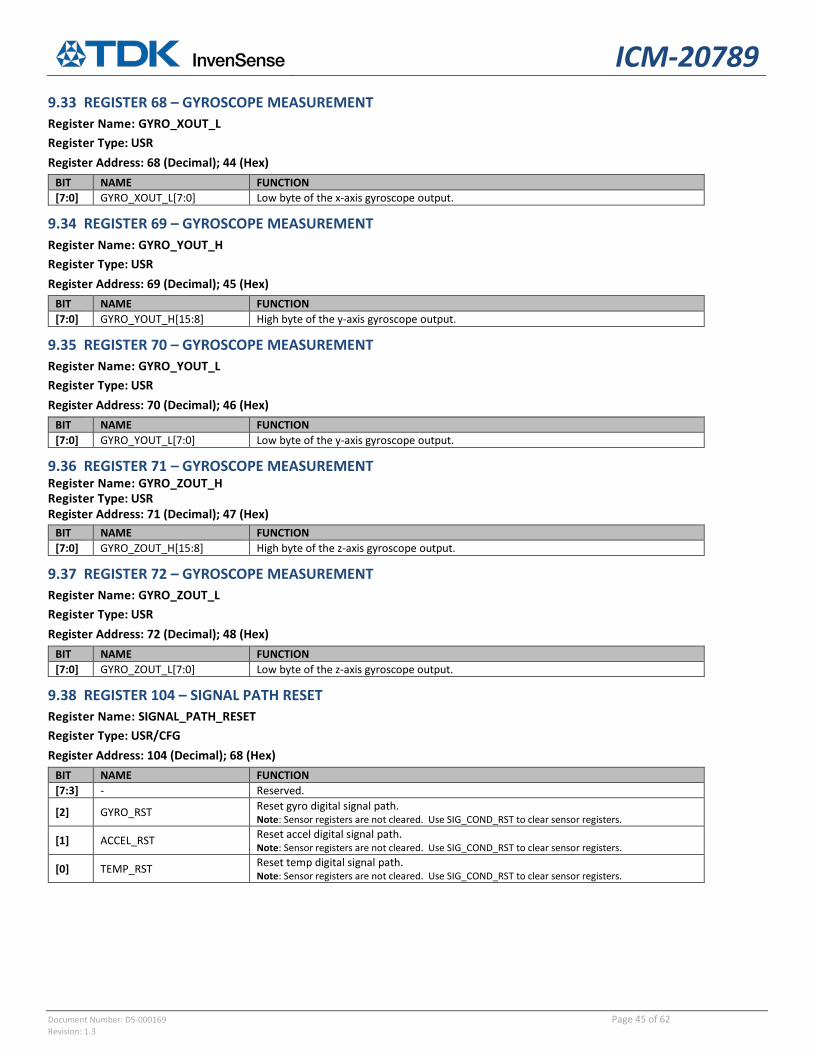
[5] - Reserved. [4] I2C_IF_DIS 1 – Reset I2C Slave module. [3] DMP_RST 1 – Reset DMP module. Reset is asynchronous. This bit auto clears after one clock cycle. [2] FIFO_RST 1 – Reset FIFO module. Reset is asynchronous. This bit auto clears after one clock cycle. [1] - Reserved.
[0] SIG_COND_RST 1 – Reset all gyro digital signal path, accel digital signal path, and temp digital signal path. This bit also clears all the sensor registers. SIG_COND_RST is a pulse of one clk8M wide.
ICM-20789
Document Number: DS-000169 Page 47 of 62 Revision: 1.3
[7] DEVICE_RESET 1 – Reset the internal registers and restores the default settings. The bit automatically clears to 0 once the reset is done.
[6] SLEEP 1 – The chip is set to sleep mode. Note: The default value is 1; the chip comes up in Sleep mode
[5] ACCEL_CYCLE
When set to 1, and SLEEP and STANDBY are not set to 1, the chip will cycle between sleep and taking a single accelerometer sample at a rate determined by SMPLRT_DIV Note: When all accelerometer axes are disabled via PWR_MGMT_2 register bits and cycle is enabled, the chip will wake up at the rate determined by the respective registers above, but will not take any samples.
[4] GYRO_STANDBY When set, the gyro drive and pll circuitry are enabled, but the sense paths are disabled. This is a low power mode that allows quick enabling of the gyros.
[3] TEMP_DIS When set to 1, this bit disables the temperature sensor.
[2:0] CLKSEL[2:0]
Code Clock Source 0 Internal 20 MHz oscillator 1 Auto selects the best available clock source – PLL if ready, else use the Internal oscillator 2 Auto selects the best available clock source – PLL if ready, else use the Internal oscillator 3 Auto selects the best available clock source – PLL if ready, else use the Internal oscillator 4 Auto selects the best available clock source – PLL if ready, else use the Internal oscillator 5 Auto selects the best available clock source – PLL if ready, else use the Internal oscillator 6 Internal 20 MHz oscillator 7 Stops the clock and keeps timing generator in reset
BIT NAME FUNCTION [7:5] NOT IMPLEMENTED Hard coded to ‘000’.
[4:0] FIFO_COUNTH[12:8] High Bits, count indicates the number of written bytes in the FIFO. Reading this byte latches the data for both FIFO_COUNTH, and FIFO_COUNTL.
ICM-20789
Document Number: DS-000169 Page 48 of 62 Revision: 1.3
[7:0] FIFO_COUNTL[7:0] Low Bits, count indicates the number of written bytes in the FIFO. NOTE: Must read FIFO_COUNTH to latch new data for both FIFO_COUNTH and FIFO_COUNTL.
BIT NAME FUNCTION [7:0] FIFO_R_W[7:0] Read/Write command provides Read or Write operation for the FIFO.
Description:
This register is used to read and write data from the FIFO buffer.
Data is written to the FIFO in order of register number (from lowest to highest). If all the FIFO enable flags (see below) are enabled, the contents of registers 59 through 72 will be written in order at the Sample Rate.
The contents of the sensor data registers (Registers 59 to 72) are written into the FIFO buffer when their corresponding FIFO enable flags are set to 1 in FIFO_EN (Register 35).
If the FIFO buffer has overflowed, the status bit FIFO_OFLOW_INT is automatically set to 1. This bit is located in INT_STATUS (Register 58). When the FIFO buffer has overflowed, the oldest data will be lost and new data will be written to the FIFO unless register 26 CONFIG, bit[6] FIFO_MODE = 1.
If the FIFO buffer is empty, reading register FIFO_DATA will return a unique value of 0xFF until new data is available. Normal data is precluded from ever indicating 0xFF, so 0xFF gives a trustworthy indication of FIFO empty.
9.46 REGISTER 117 – WHO AM I Register Name: WHOAMI Register Type: USR/CFG Register Address: 117 (Decimal); 75 (Hex)
BIT NAME FUNCTION [7:0] WHOAMI Register to indicate to user which device is being accessed.
This register is used to verify the identity of the device. The contents of WHOAMI is an 8-bit device ID.
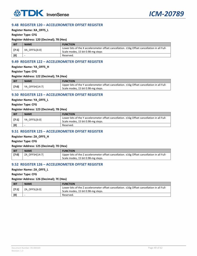
[7:1] ZA_OFFSL[6:0] Lower bits of the Z accelerometer offset cancellation. ±16g Offset cancellation in all Full-Scale modes, 15 bit 0.98-mg steps.
[0] - Reserved.
ICM-20789
Document Number: DS-000169 Page 50 of 62 Revision: 1.3
10 PRESSURE SENSOR – HOW TO READ 10.1 I2C OPERATION AND COMMUNICATION All commands and memory locations of the ICM-20789 are mapped to a 16-bit address space which can be accessed via the I2C protocol.
Upon VDD reaching the power-up voltage level VPOR, the ICM-20789 enters idle state after a duration of tPU. In idle state, the ICM-20789 is ready to receive commands from the master (microcontroller).
Each transmission sequence begins with START condition (S) and ends with an (optional) STOP condition (P) as described in the I2C-bus specification. Whenever the sensor is powered up, but not performing a measurement or communicating, it automatically enters idle state for energy saving.
Measurement Commands
The ICM-20789 provides the possibility to define the sensor behavior during measurement as well as the transmission sequence of measurement results. These characteristics are defined by the appropriate measurement command (see Table 24). Each measurement command triggers both a temperature and a pressure measurement.
OPERATION MODE TRANSMIT T FIRST TRANSMIT P FIRST Low Power (LP) 0x609C 0x401A
Normal (N) 0x6825 0x48A3 Low Noise (LN) 0x70DF 0x5059
Ultra-Low Noise (ULN) 0x7866 0x58E0
Table 24. Measurement Commands
Starting a Measurement
A measurement communication sequence consists of a START condition followed by the I2C header with the 7-bit I2C device address and a write bit (write W: ‘0’, 8-bit word including I2C header: 0xC6). The sensor indicates the proper reception of a byte by pulling the SDA pin low (ACK bit) after the falling edge of the 8th SCL clock. Then the sensor is ready to receive a 16-bit measurement command. Again, the ICM-20789 acknowledges the proper reception of each byte with ACK condition. With the acknowledgement of the measurement command, the ICM-20789 starts measuring pressure and temperature.
Sensor Behavior during Measurement
In general, the sensor does not respond to any I2C activity during measurement, i.e. I2C read and write headers are not acknowledged (NACK).
Readout of Measurement Results
After a measurement command has been issued and the sensor has completed the measurement, the master can read the measurement results by sending a START condition followed by an I2C read header (8-bit word including I2C header: 0xC7). The sensor will acknowledge the reception of the read header and send the measured data in the specified order to the master. The MSB of the corresponding data is always transmitted first. Temperature data is transmitted in two 8-bit words and pressure data is transmitted in four 8-bit words. Regarding the pressure data, only the first three words MMSB, MLSB and LMSB contain information about the ADC pressure value. Therefore, for retrieving the ADC pressure value, LLSB must be disregarded:
pdout = MMSB ≪ 16 | MLSB ≪ 8| LMSB. Two bytes of data are always followed by one byte CRC checksum, for calculation see the Checksum Calculation section. Each byte must be acknowledged by the microcontroller with an ACK condition for the sensor to continue sending data. If the ICM-20789 does not receive an ACK from the master after any byte of data, it will not continue sending data.
ICM-20789
Document Number: DS-000169 Page 51 of 62 Revision: 1.3
Whether the sensor sends out pressure or temperature data first depends on the measurement command that was sent to the sensor to initiate the measurement. The I2C master can abort the read transfer with a NACK condition after any data byte if it is not interested in subsequent data, e.g. the CRC byte or the second measurement result, in order to save time.
Soft Reset
The ICM-20789 provides a soft reset mechanism that forces the system into a well-defined state without removing the power supply. If the system is in idle state (i.e. if no measurement is in progress) the soft reset command will be accepted by ICM-20789. This triggers the sensor to reset all internal state machines and reload calibration data from the memory.
The ICM-20789 has an ID register which contains a specific product code. The read-out of the ID register can be used to verify the presence of the sensor and proper communication. The command to read the ID register is shown in Table 21.
Command Hex Code Binary Code Read ID Register 0xEFC8 1110’1111’1100’1000
Table 26. Read-Out Command of ID Register
It needs to be sent to the ICM-20789 after an I2C write header. After the ICM-20789 has acknowledged the proper reception of the command, the master can send an I2C read header and the ICM-20789 will submit the 16-bit ID followed by 8 bits of CRC. The structure of the ID is described in Table 22.
Table 27. Structure of the 16-bit ID
Bits 15:6 of the ID contain unspecified information (marked as “x”), which may vary from sensor to sensor, while bits 5:0 contain the ICM-20789-specific product code.
Checksum Calculation
The 8-bit CRC checksum transmitted after each data word is generated by a CRC algorithm with the properties displayed in Table 23. The CRC covers the contents of the two previously transmitted data bytes.
Pressure measurement data is always transferred as 4 8-bit words; temperature measurement data is always transferred as two 8-bit words. Please see Readout of Measurement Results (Page 44) for more details.
ICM-20789
Document Number: DS-000169 Page 52 of 62 Revision: 1.3
Temperature measurement values t_dout are linearized by the ICM-20789 and must be calculated to °C by the user via the following formula:
T = - 45°C + (175°C / 216) x t_dout
For retrieving physical pressure values in Pa the following conversion formula has to be used:
P = A + B / (C + pdout)
where pdout is the sensor’s raw pressure output. The converted output is compensated for temperature effects via the temperature dependent functions A, B and C. Besides the raw temperature output t_dout, the calculation of A, B and C requires to access calibration parameters OTP0, OTP1, OTP2, OTP3 stored in the OTP of the sensor.
Full sample code for calculating physical pressure values is given in the Sample Code section. The general workflow of the conversion is done by:
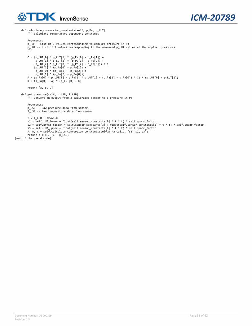
1) Import class Invensense_pressure_conversion 2) Read out values OTP0, …, OTP3 and save to c1, …, c4 3) Create object name for an individual sensor with parameter values c1, …, c4 name = Invensense_pressure_conversion ([c1,c2,c3,c4]) 4) Get raw pressure p_dout and temperature t_dout data from the sensor as described in chapter Readout of Measurement Results. 5) Call function get_pressure: name.get_pressure(p_dout, t_dout)
The Sample Code section gives an example of this workflow.
Read-out of calibration parameters
For converting raw pressure data to physical values, four calibration parameters have to be retrieved from the OTP of the sensor.
Set up of OTP read:
1) Send I2C write header 0xC6 2) Send command 0xC595 (move pointer in address register) 3) Send address parameter together with its CRC 0x00669C
Steps 1) – 3) can be done on many platforms by a single I2C write of the value 0xC59500669C.
Read out parameters:
Repeat the following procedure 4 times:
a. Send I2C write header 0xC6 b. Send command 0xC7F7 (incremental read-out of OTP) c. Send I2C read header 0xC7 d. Read 3Byte (2Byte of data and 1Byte of CRC) e. Decode data as 16-bit big endian signed integer and store result into n-th calibration parameter cn.
Steps a) to d) can be done on many platforms by a single write 0xC7F7 to the chip address followed by a single read of 3 Byte from the chip slave device address.
Sample Pseudo Code: conversion formula (exemplary python syntax) class Invensense_pressur_Conversion: """ Class for conversion of the pressure and temperature output of the Invensense sensor""" def __init__(self, sensor_constants): """ Initialize customer formula Arguments: sensor_constants -- list of 4 integers: [c1, c2, c3, c4] """ self.sensor_constants = sensor_constants # configuration for Pressure Samples self.p_Pa_calib = [45000.0, 80000.0, 105000.0] self.LUT_lower = 3.5 * (2**20) self.LUT_upper = 11.5 * (2**20) self.quadr_factor = 1 / 16777216.0 self.offst_factor = 2048.0
ICM-20789
Document Number: DS-000169 Page 53 of 62 Revision: 1.3
def calculate_conversion_constants(self, p_Pa, p_LUT): """ calculate temperature dependent constants Arguments: p_Pa -- List of 3 values corresponding to applied pressure in Pa p_LUT -- List of 3 values corresponding to the measured p_LUT values at the applied pressures. """ C = (p_LUT[0] * p_LUT[1] * (p_Pa[0] - p_Pa[1]) + p_LUT[1] * p_LUT[2] * (p_Pa[1] - p_Pa[2]) + p_LUT[2] * p_LUT[0] * (p_Pa[2] - p_Pa[0])) / \ (p_LUT[2] * (p_Pa[0] - p_Pa[1]) + p_LUT[0] * (p_Pa[1] - p_Pa[2]) + p_LUT[1] * (p_Pa[2] - p_Pa[0])) A = (p_Pa[0] * p_LUT[0] - p_Pa[1] * p_LUT[1] - (p_Pa[1] - p_Pa[0]) * C) / (p_LUT[0] - p_LUT[1]) B = (p_Pa[0] - A) * (p_LUT[0] + C) return [A, B, C] def get_pressure(self, p_LSB, T_LSB): """ Convert an output from a calibrated sensor to a pressure in Pa. Arguments: p_LSB -- Raw pressure data from sensor T_LSB -- Raw temperature data from sensor """ t = T_LSB - 32768.0 s1 = self.LUT_lower + float(self.sensor_constants[0] * t * t) * self.quadr_factor s2 = self.offst_factor * self.sensor_constants[3] + float(self.sensor_constants[1] * t * t) * self.quadr_factor s3 = self.LUT_upper + float(self.sensor_constants[2] * t * t) * self.quadr_factor A, B, C = self.calculate_conversion_constants(self.p_Pa_calib, [s1, s2, s3]) return A + B / (C + p_LSB) [end of the pseudocode]
ICM-20789
Document Number: DS-000169 Page 54 of 62 Revision: 1.3
Sample code: using conversion formula (exemplary python syntax) def read_otp_from_i2c(): # TODO: implement read from I2C # refer to data sheet for I2C commands to read OTP return 1000, 2000, 3000, 4000 def read_raw_pressure_temp_from_i2c(): # TODO: implement read from I2C # refer to data sheet for I2C commands to read pressure and temperature return 8000000, 32000 # Sample code to read from Invensense_pressure_conversion import Invensense_pressure_conversion # -- initialization c1, c2, c3, c4 = read_otp_from_i2c() conversion = Invensense_pressure_conversion([c1, c2, c3, c4]) # -- read raw pressure and temp data, calculate pressure p, T = read_raw_pressure_temp_from_i2c() pressure = conversion.get_pressure(p, T) print 'Pressure: %f' % pressure [end of the pseudocode]
Communication Data Sequences
Figure 15. Communication Sequence for starting a measurement and reading measurement results
ICM-20789
Document Number: DS-000169 Page 55 of 62 Revision: 1.3
11 ASSEMBLY This section provides general guidelines for assembling TDK-InvenSense Micro Electro-Mechanical Systems (MEMS) gyros packaged in LGA package.
11.1 ORIENTATION OF AXES The diagram below shows the orientation of the axes of sensitivity and the polarity of rotation. Note the pin 1 identifier (•) in the figure.
ICM-20789
+Z
+X
+Y
+Z
+Y
+X
Figure 16. Orientation of Axes of Sensitivity and Polarity of Rotation
11.2 IMPLEMENTATION AND USAGE RECOMMENDATIONS Soldering
When soldering, use the standard soldering profile IPC/JEDEC J-STD-020 with peak temperatures of 260°C. ICM-20789 may exhibit a pressure offset after soldering, some settling time may be required depending on soldering properties, PCB properties, and ambient conditions.
The ICM-20789 is an open cavity package, it is mandatory to use no-clean solder paste and no board wash should be applied. The ICM-20789 should be limited to a single reflow and no rework is recommended.
Chemical Exposure and Sensor Protection
The ICM-20789 is an open cavity package and therefore should not be exposed to particulates or liquids. If any type of protective coating must be applied to the circuit board, the sensor must be protected during the coating process.
ICM-20789
Document Number: DS-000169 Page 56 of 62 Revision: 1.3
11.3 PACKAGE DIMENSIONS 24 Lead LGA (4 mm x 4 mm x 1.365 mm) NiPdAu Lead-frame finish
Figure 17. Package Dimensions
DIMENSIONS IN MILLIMETERS
SYMBOLS MIN NOM MAX A 1.265 1.365 1.465
A3 --- 1.185 REF. --- b 0.20 0.25 0.30 c --- 0.18 REF. --- D 3.90 4.00 4.10 E 3.90 4.00 4.10 e --- 0.50 --- L 0.35 0.45 0.55
L1 0.025 0.075 0.125 L3 0.325 0.375 0.425
Table 29. Package Dimensions Table
Figure 18 shows the recommended PCB land pattern for ICM-20789.
ICM-20789
Document Number: DS-000169 Page 57 of 62 Revision: 1.3
Figure 18. ICM-20789 recommended PCB land pattern
ICM-20789
Document Number: DS-000169 Page 58 of 62 Revision: 1.3
12 PART NUMBER PACKAGE MARKING The part number package marking for ICM-20789 devices is summarized below:
PART NUMBER PART NUMBER PACKAGE MARKING ICM-20789 IC2789
IC2789X X X X X XXX YYWW
Lot Traceability Code
Y Y = Year CodeW W = Work Week
TOP VIEW
Part Number
Figure 19. Part Number Package Marking
ICM-20789
Document Number: DS-000169 Page 59 of 62 Revision: 1.3
13 ORDERING GUIDE PART TEMP RANGE PACKAGE QUANTITY PACKAGING
ICM-20789† −40°C to +85°C 24-Pin LGA 3,000 13” Tape and Reel
†Denotes RoHS and Green-Compliant Package
ICM-20789
Document Number: DS-000169 Page 60 of 62 Revision: 1.3
14 REFERENCE Please refer to “InvenSense MEMS Handling Application Note (AN-IVS-0002A-00)” for the following information:
• Manufacturing Recommendations o Assembly Guidelines and Recommendations o PCB Design Guidelines and Recommendations o MEMS Handling Instructions o ESD Considerations o Reflow Specification o Storage Specifications o Package Marking Specification o Tape & Reel Specification o Reel & Pizza Box Label o Packaging o Representative Shipping Carton Label
• Compliance o Environmental Compliance o DRC Compliance o Compliance Declaration Disclaimer
ICM-20789
Document Number: DS-000169 Page 61 of 62 Revision: 1.3
10/31/17 1.3 Updated Ordering Guide, Clarified Pin Connections as NC, GND, or VDD
ICM-20789
Document Number: DS-000169 Page 62 of 62 Revision: 1.3
This information furnished by InvenSense, Inc. (“InvenSense”) is believed to be accurate and reliable. However, no responsibility is assumed by InvenSense for its use, or for any infringements of patents or other rights of third parties that may result from its use. Specifications are subject to change without notice. InvenSense reserves the right to make changes to this product, including its circuits and software, in order to improve its design and/or performance, without prior notice. InvenSense makes no warranties, neither expressed nor implied, regarding the information and specifications contained in this document. InvenSense assumes no responsibility for any claims or damages arising from information contained in this document, or from the use of products and services detailed therein. This includes, but is not limited to, claims or damages based on the infringement of patents, copyrights, mask work and/or other intellectual property rights.
Certain intellectual property owned by InvenSense and described in this document is patent protected. No license is granted by implication or otherwise under any patent or patent rights of InvenSense. This publication supersedes and replaces all information previously supplied. Trademarks that are registered trademarks are the property of their respective companies. InvenSense sensors should not be used or sold in the development, storage, production or utilization of any conventional or mass-destructive weapons or for any other weapons or life threatening applications, as well as in any other life critical applications such as medical equipment, transportation, aerospace and nuclear instruments, undersea equipment, power plant equipment, disaster prevention and crime prevention equipment.