Infrared Imaging Components for Use in Automotive Safety Applications Confidential Page 1 of 24 DOCUMENT DELIVERABLE NUMBER D3.2 DUE DATE 1.9.2011 TYPE OF DELIVERABLE REPORT ACTUAL DATE 07.09.2011 ISSUED BY SENSONOR PAGES 24 CONTRIBUTING WP / TASK WP3/ TASK 3.2 ANNEXES 0 CONFIDENTIALITY STATUS RESTRICTED TO GROUP (RE) PROJECT GRANT AGREEMENT NO. 223989 ACRONYM ICU TITLE INFRARED IMAGING COMPONENTS FOR USE IN AUTOMOTIVE SAFETY APPLICATIONS PROJECT START 01.05.2008 CALL FP7-ICT-2007.3.5 FUNDING SCHEME STREP PROJECT WEBSITE WWW.ICU-EU.COM ICU PROJECT DELIVERABLE LEAD BENEFICIARY SENSONOR AUTHOR MARTIN BRING PHONE: +47 33035264 E-MAIL: MARTIN.BRING@SENSONOR.NO PROJECT COORDINATOR KTH - ROYAL INSTITUTE OF TECHNOLOGY PROJECT COORDINATOR REPRESENTATIVE DR. FRANK NIKLAUS PHONE: +46-8-790 9332 E-MAIL: FRANK.NIKLAUS@EE.KTH.SE PROJECT OFFICER DR. MICHAEL ZIEGLER EUROPEAN COMMISSION DELIVERABLE D3.2 Process and design concepts for implementation of wafer level packaging of 320x240 pixels on CMOS wafer
Transcript
Infrared Imaging Components for Use in Automotive Safety Applications
Confidential
Page 1 of 24
DOCUMENT DELIVERABLE NUMBER D3.2 DUE DATE 1.9.2011 TYPE OF DELIVERABLE REPORT ACTUAL DATE 07.09.2011 ISSUED BY SENSONOR PAGES 24 CONTRIBUTING WP / TASK WP3/ TASK 3.2 ANNEXES 0 CONFIDENTIALITY STATUS RESTRICTED TO GROUP (RE) PROJECT GRANT AGREEMENT NO. 223989 ACRONYM ICU
TITLE INFRARED IMAGING COMPONENTS FOR USE IN AUTOMOTIVE SAFETY APPLICATIONS
1 Coordinator KTH - Royal Institute of Technology KTH Sweden
2 Acreo AB Acreo Sweden
3 Sensonor Technologies AS SensoNor Norway
4 Autoliv Development AB Autoliv Sweden
5 Umicore nv Umicore Belgium
6 Vrije Universiteit Brussel VUB Belgium
Version: 1.0 Date: 07.09.2011
Deliverable D3.2
Process and design concepts for implementation of wafer level packaging of 320x240 pixels on CMOS wafer
Confidential
Page 3 of 24
TABLE OF CONTENTS
1. Executive summary ................................................................................................................... 4 2. Introduction ............................................................................................................................... 5 2.1 Purpose of this document .................................................................................................. 5 2.2 Statement of the problem and scientific methodology ...................................................... 5 2.3 Related work packages and tasks ...................................................................................... 6 3. Wafer level vacuum package and cap design ........................................................................... 7 3.1 Cap wafer design ............................................................................................................... 7 3.2 Preparation of the FPA wafer ............................................................................................ 8 3.3 Fabrication of the cap wafer .............................................................................................. 9 3.4 Cap wafer bonding ........................................................................................................... 10 3.5 Process compatibility ....................................................................................................... 11 3.6 Cap wafer resizing ........................................................................................................... 13 3.7 Getter definition ............................................................................................................... 15 3.8 Wafer level vacuum encapsulation and dicing ................................................................ 17 3.9 Residual gas analysis and Ar outgassing ......................................................................... 18 4. Collaborations within the consortium ..................................................................................... 20 5. Conclusions ............................................................................................................................. 20 6. List of references ..................................................................................................................... 21 7. List of Figures ......................................................................................................................... 22 8. List of tables ............................................................................................................................ 23 9. List of acrynoms...................................................................................................................... 24
Version: 1.0 Date: 07.09.2011
Deliverable D3.2
Process and design concepts for implementation of wafer level packaging of 320x240 pixels on CMOS wafer
Confidential
Page 4 of 24
1. Executive summary The activities in task 3.2 started in month 9 of the project and have recently been finalized. Conclusions from experimental and theoretical work presented in D3.1 of the ICU project [1] show that the viability of the Cu/Sn SLID wafer bonding technology can be motivated and it is fully aligned with the most suitable strategy for assembly of lens modules. Hence, the pursued and herein presented wafer level vacuum encapsulation technology is based on Cu/Sn SLID bonding. Both the CMOS wafer containing the bolometers and the cap wafer need to be prepared for the Cu/Sn SLID bonding. Process concepts for both wafers have been developed and experimentally verified. Apart from the Cu/Sn bond frames, the cap wafer also features recesses, patterned multi-layer anti-reflective coatings (ARC) and thin film getters. The ARC significantly increases the IR transmittance while the getter is needed to maintain vacuum throughout the lifetime of the product. In order to accommodate the ARC, getter and cap deflection due to vacuum the cap wafer is recessed. The process compatibility of the different materials has been carefully investigated and a process concept with virtually no effect on the getter’s and ARC’s performance has been developed. The developed process concept reduces the number of photolithographic steps by utilizing the getter as optical shield for the blind pixels, used as e.g. reference or pressure sensor pixels. The dual functionality getter design has been finalized and successfully implemented on the cap wafers. It has been experimentally verified that the getter complies with the design rules laid out in D3.1 [1]. The Ar outgassing from the ROIC has been quantified and it is higher than what can be allowed. Different ways to reduce the outgassing have been investigated. It was found that depositing an Ar diffusion barrier in the form of an Al2O3 layer is sufficient to lower the Ar outgassing to an acceptable level. Cap wafers featuring recesses, patterned multi-layer anti-reflective coatings, thin film getters, and Cu/Sn bond frames have been successfully fabricated and bonded to CMOS wafers containing bolometers. The integrated pressure sensor indicated that the pressure was too high. To learn more about the composition of the gas in the cavity residual gas analysis (RGA) was performed on some devices. The RGA showed that the main component was Ar. The results from the RGA combined with additional outgassing measurements have been used to find the source of the Ar and it can be eliminated. The expected Ar partial pressure is within the target pressure of 1Pa once it is eliminated. ICU Project Website: www.icu-eu.com
Version: 1.0 Date: 07.09.2011
Deliverable D3.2
Process and design concepts for implementation of wafer level packaging of 320x240 pixels on CMOS wafer
Confidential
Page 5 of 24
2. Introduction
2.1 Purpose of this document This D3.2 deliverable report summarizes the development work performed on wafer level vacuum encapsulation of the FPAs on CMOS wafer.
2.2 Statement of the problem and scientific methodology The performance of uncooled bolometer FIR detectors is strongly related to a well-controlled heat transfer from each pixel. The transport of heat determines the thermal time constant of the bolometer which must be carefully tuned. A very small time constant increases the pixel NETD while a large time constant results in an image which fall behinds. The aim is to design the pixels in such a way that the heat is transported essentially only through the support legs. As a result, the bolometer pixels must be surrounded with vacuum. For present uncooled FIR thermal imagers, hermetic vacuum cavities are achieved by a sealing process in the BE line. Either is the process performed in vacuum followed by a getter activation annealing step, or is the assembling performed in atmospheric ambient followed by vacuum pumping through a metal tube which is subsequentially hermetically sealed. These processes are in most cases accomplished on chip level and contribute therefore substantially to the overall cost. Consequently, it is a considerable interest in wafer level packaging of FPAs in vacuum, thereby reducing process times and costs. Today only L3 Communications and FLIR have presented thermal imaging products assembled at the wafer level [2], but LETI together with ULIS have announced that they are developing novel methods for wafer level packaging of FIR detector arrays [3]. Except from the fact that the encapsulation process used for the ICU demonstrator must be compatible with the most viable concept for 1st level camera optics (developed in WP5 and WP6), high bond strength, hermeticity and low temperature processes are three important requirements which limit the number of potential technologies for packaging of the FPAs. For example, anodic bonding between glass and Si is a low-temperature technology and well-established in Sensonor’s production line. Glass is however not transparent for FIR wavelengths, and can therefore not be used as a window. Glass frit bonding requires relatively wide bonded regions in order to fulfill the hermeticity requirements while adhesive bonding is not hermetic. Direct bonding, e.g. SiO2/SiO2 bonding, requires extremely well-prepared and flat surfaces as well as wide bonding regions to be hermetic. Low temperature metal bonding is hermetic and is therefore the most promising bonding technology for FPA vacuum encapsulation. Technologies based on soldering have been evaluated and tested thoroughly in the FNIR project. Au/Sn or Cu/Sn are two material systems that have attracted our attention. Even though Au/Sn eutectic bonding is a well-known technology, it is more commonly used as solder bumps in chip-to-wafer processes [4]-[6]. The Cu/Sn SLID technology is also mostly investigated on chip level for interconnect formation in 3D integration [7], but has been found to be the most suitable process for encapsulation of IR microbolometer arrays [8]. Previous limited small-scale laboratory experiments related to hermetic sealing at the wafer level shows an unacceptably high leak rate compared to the requirements for FIR automotive systems [9]. Therefore, there is an extensive demand for development of the Cu/Sn SLID technology from being a typical chip-to-wafer process to be an industrial technology for high volume production while at
Version: 1.0 Date: 07.09.2011
Deliverable D3.2
Process and design concepts for implementation of wafer level packaging of 320x240 pixels on CMOS wafer
Confidential
Page 6 of 24
the same time accomplishing hermetic sealing with leak rates down to ∼10-14 mbar /s range. In this project, the maximum pressure after wafer level packaging is set to 1Pa. Simulations have confirmed that the heat conduction in gas is negligible compared to the transport through the bolometer support legs for lower pressures. The low pressure requires thin film getters to guarantee the vacuum conditions throughout the lifetime of the product. The feasibility of thermo-compression bonding has been studied in parallel in this project. State-of-the-art wafer bonding equipment can apply a high force to the wafers, thus enabling hermetic sealing. The degree of success is however depending on the design of the bond frames. Conclusions from experimental and theoretical work presented in D3.1 of the ICU project [1] show that the viability of the Cu/Sn SLID wafer bonding technology can be motivated and it is fully aligned with the most suitable strategy for assembling of lens modules. Hence, the pursued and herein presented wafer level vacuum encapsulation technology is based on Cu/Sn SLID bonding. In addition, results from experimental work regarding the Si cap wafer including getter and ARC are compared to the design rules laid out in D.3.1 in the ICU project [1].
2.3 Related work packages and tasks The concept for integration of the bond frames on the CMOS wafer has been developed in cooperation with Acreo, which is responsible for fabricating the bolometers on the CMOS wafer in WP4. The concepts for the integrated FIR camera optics in WP5 have been analyzed with respect to vacuum encapsulation. The concepts were proposed in cooperation with Umicore, which develop the lens materials in WP6 [10].
Version: 1.0 Date: 07.09.2011
Deliverable D3.2
Process and design concepts for implementation of wafer level packaging of 320x240 pixels on CMOS wafer
Confidential
Page 7 of 24
3. Wafer level vacuum package and cap design In this work package, studies on wafer level vacuum bonding technologies and designs that are compatible with concepts for integrated optics have been conducted. Conclusions from experimental and theoretical work presented in D3.1 of the ICU project [1] show that the viability of the Cu/Sn SLID wafer bonding technology can be motivated and it is fully aligned with the most suitable strategy for assembling of lens modules. Hence, the pursued and herein presented wafer level vacuum encapsulation technology is based on Cu/Sn SLID bonding. In addition, results from experimental work regarding the Si cap wafer including getter and ARC are compared to the design rules laid out in D.3.1 in the ICU project [1].
3.1 Cap wafer design The performance of uncooled microbolometers depends on a range of factors [11]. Some of those factors are directly influenced by the capping technology and need to be considered when designing the cap. One of those factors is the pressure in the package. From a performance point of views it is desirable to minimize the heat transfer through residual gas in the cavity. At pressures below 1Pa the heat transfer through residual gas is negligible and the pixel’s total heat transfer is dominated by the contribution from the legs. To tackle the challenge of maintaining such a low pressure during the lifetime of the device a high performance getter is essential. In principle there are two main groups of getters, evaporable getters (EG) and non-evaporable getters (NEG). For this technology a thin film NEG has been chosen due to its simplified integration scheme. The performance of a NEG is closely related to the activation temperature. A higher activation temperature gives better performance. On the other hand, outgassing from e.g. the ROIC increases with elevated temperatures. This implies that there may be an optimum activation temperature that lies below the maximum allowed temperature that is typically limited by the ROIC. Another factor that is relevant to consider when designing the cap wafer is the transmission of infrared radiation. To reduce the absorption in the silicon, a high purity material with low oxygen concentration is needed. FZ silicon is the typical material of choice for this application, but magnetic CZ can also be considered since it can achieve significantly lower oxygen concentrations than standard CZ. The thickness of the cap wafer is a tradeoff between the need to minimize the absorption of the incoming IR radiation, wherein the thinner the wafer the better, and the requirements for low wafer bow introduced by the stress in deposited films and for safe handling in production. To further increase the transmission an anti-reflective coating (ARC) is added. In order to avoid excessive heating from solar radiation which would otherwise damage the FPA, the ARC is designed to block wavelengths below 6µm. For this purpose a multilayer ARC has been chosen. A high IR transmittance through the cap is required to have a strong signal reaching the active pixels. On the other hand the reference pixels need to be shielded from all incident IR radiation. This can be achieved by placing a metal film on the correct location on the cap. To reduce the number of masks and process steps it is possible to use the getter for this purpose if the design is made properly. Figure 1 shows the getter design used for the cap wafers. This getter is designed according to the design rules laid out in D.3.1 in the ICU project [1] allowing for a >100µm overlap over the blind pixels while at the same time not overlapping with the active pixels.
Version: 1.0 Date: 07.09.2011
Deliverable D3.2
Process and design concepts for implementation of wafer level packaging of 320x240 pixels on CMOS wafer
Confidential
Page 8 of 24
Figure 1. Getter design used for the cap wafer. All values are in mm.
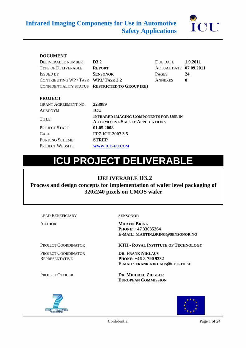
3.2 Preparation of the FPA wafer The FPA wafer realized in WP4 consists of a ROIC substrate on which a bolometer superstructure is integrated. As illustrated in Figure 2a) the FPA pixels are completely embedded in a sacrificial layer before starting the fabrication of the bond frames. This protects the sensitive FPA pixels from mechanical and chemical effects during the processing. One of the major concerns when dealing with vacuum encapsulation on ROIC wafers is outgassing of Ar. Because Ar is not captured by the getter any Ar that gasses out into the cavity will inevitably increase the pressure. The Ar originates from the fabrication of the ROIC where Ar is a very common process gas. Since Ar outgassing from the ROIC is a known problem, different methods that can be used to reduce it were investigated at an early stage. The experiments and results are described more in detail below but it was found that Al2O3 was an effective barrier preventing Ar from reaching the cavity. In order to reduce the Ar outgassing, an Ar diffusion barrier is deposited on top of the ROIC early in the process before depositing the sacrificial layer. In order not to place the bond frames directly on the sacrificial layer, this is removed in regions around the FPA as illustrated in Figure 2a). The FPA pixels are at this stage still fully embedded in the remaining sacrificial layer.
Version: 1.0 Date: 07.09.2011
Deliverable D3.2
Process and design concepts for implementation of wafer level packaging of 320x240 pixels on CMOS wafer
Confidential
Page 9 of 24
Next the Cu-Sn bond frames are electroplated to a nominal thickness of 5µm Cu and 1.5µm Sn [4], as illustrated in Figure 2b). The seed layer used during the electroplating of the bond frames is deposited and patterned on the FPA wafer before the formation of the bolometers. The sacrificial layer etching illustrated in Figure 2c) releases the bolometers and clears the wire bond pads. The FPA wafer is now ready for cap wafer bonding. The fabrication of the cap wafer is described in the following section.
Figure 2. Illustration of the process flow for the formation of bond frames on the FPA wafer. a) Etching of openings in sacrificial layer down to ROIC, b) Electro plating of bond frames, and c) Etching of sacrificial layer to release bolometers.
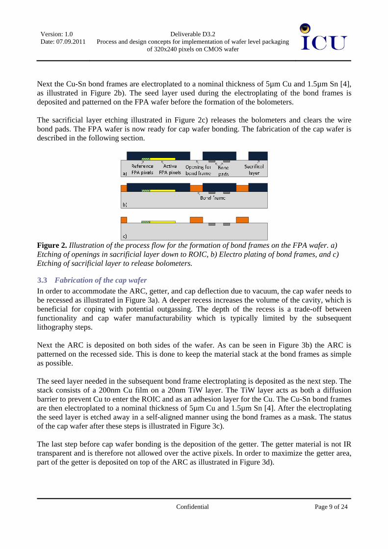
3.3 Fabrication of the cap wafer In order to accommodate the ARC, getter, and cap deflection due to vacuum, the cap wafer needs to be recessed as illustrated in Figure 3a). A deeper recess increases the volume of the cavity, which is beneficial for coping with potential outgassing. The depth of the recess is a trade-off between functionality and cap wafer manufacturability which is typically limited by the subsequent lithography steps. Next the ARC is deposited on both sides of the wafer. As can be seen in Figure 3b) the ARC is patterned on the recessed side. This is done to keep the material stack at the bond frames as simple as possible. The seed layer needed in the subsequent bond frame electroplating is deposited as the next step. The stack consists of a 200nm Cu film on a 20nm TiW layer. The TiW layer acts as both a diffusion barrier to prevent Cu to enter the ROIC and as an adhesion layer for the Cu. The Cu-Sn bond frames are then electroplated to a nominal thickness of 5µm Cu and 1.5µm Sn [4]. After the electroplating the seed layer is etched away in a self-aligned manner using the bond frames as a mask. The status of the cap wafer after these steps is illustrated in Figure 3c). The last step before cap wafer bonding is the deposition of the getter. The getter material is not IR transparent and is therefore not allowed over the active pixels. In order to maximize the getter area, part of the getter is deposited on top of the ARC as illustrated in Figure 3d).
Version: 1.0 Date: 07.09.2011
Deliverable D3.2
Process and design concepts for implementation of wafer level packaging of 320x240 pixels on CMOS wafer
Confidential
Page 10 of 24
Figure 3. Illustration of the cap wafer process flow. a) Recess etching, b) deposition of ARC, c) Seed layer deposition and electro plating of bond frames with subsequent removal of seed layer,
and d) Deposition of getter.
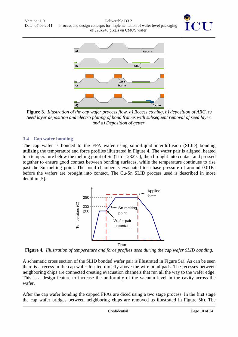
3.4 Cap wafer bonding The cap wafer is bonded to the FPA wafer using solid-liquid interdiffusion (SLID) bonding utilizing the temperature and force profiles illustrated in Figure 4. The wafer pair is aligned, heated to a temperature below the melting point of Sn (Tm = 232°C), then brought into contact and pressed together to ensure good contact between bonding surfaces, while the temperature continues to rise past the Sn melting point. The bond chamber is evacuated to a base pressure of around 0.01Pa before the wafers are brought into contact. The Cu-Sn SLID process used is described in more detail in [5].
Time
Tem
pera
ture
(C)
Appliedforce280
200
Wafer pairin contact
Sn meltingpoint
232
Figure 4. Illustration of temperature and force profiles used during the cap wafer SLID bonding.
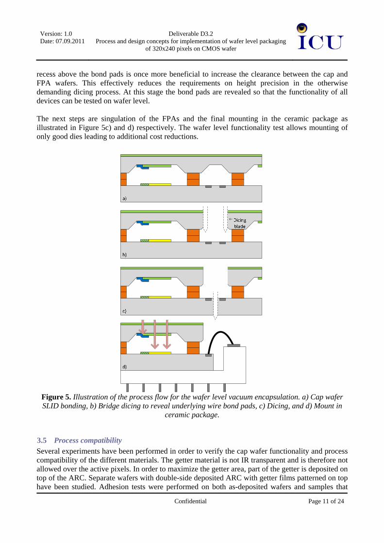
A schematic cross section of the SLID bonded wafer pair is illustrated in Figure 5a). As can be seen there is a recess in the cap wafer located directly above the wire bond pads. The recesses between neighboring chips are connected creating evacuation channels that run all the way to the wafer edge. This is a design feature to increase the uniformity of the vacuum level in the cavity across the wafer. After the cap wafer bonding the capped FPAs are diced using a two stage process. In the first stage the cap wafer bridges between neighboring chips are removed as illustrated in Figure 5b). The
Version: 1.0 Date: 07.09.2011
Deliverable D3.2
Process and design concepts for implementation of wafer level packaging of 320x240 pixels on CMOS wafer
Confidential
Page 11 of 24
recess above the bond pads is once more beneficial to increase the clearance between the cap and FPA wafers. This effectively reduces the requirements on height precision in the otherwise demanding dicing process. At this stage the bond pads are revealed so that the functionality of all devices can be tested on wafer level. The next steps are singulation of the FPAs and the final mounting in the ceramic package as illustrated in Figure 5c) and d) respectively. The wafer level functionality test allows mounting of only good dies leading to additional cost reductions.
Figure 5. Illustration of the process flow for the wafer level vacuum encapsulation. a) Cap wafer SLID bonding, b) Bridge dicing to reveal underlying wire bond pads, c) Dicing, and d) Mount in
ceramic package.
3.5 Process compatibility Several experiments have been performed in order to verify the cap wafer functionality and process compatibility of the different materials. The getter material is not IR transparent and is therefore not allowed over the active pixels. In order to maximize the getter area, part of the getter is deposited on top of the ARC. Separate wafers with double-side deposited ARC with getter films patterned on top have been studied. Adhesion tests were performed on both as-deposited wafers and samples that
Version: 1.0 Date: 07.09.2011
Deliverable D3.2
Process and design concepts for implementation of wafer level packaging of 320x240 pixels on CMOS wafer
Confidential
Page 12 of 24
were treated using the typical getter activation process, i.e. 350°C for 30 minutes. All results did show good adhesion between getter and ARC, confirming the material and process compatibility. Process compatibility experiments concerning the integration order of the getter has also been performed. It is not obvious that the getter should be integrated as the last step before bonding. An alternative approach where the getter is integrated before the bond frames has been considered. The benefit with that approach would be that the bond frames are not exposed to other processes before bonding. However the performance of the getter is reduced by almost one order of magnitude due to compatibility issues with the TiW used in the seed layer. But since the bond process is robust enough to allow for getter deposition after bond frame formation this is not a limiting factor. The influence from the cap wafer processing on the average IR transmittance in the 8µm-14µm wavelengths interval is summarized in Table 1. None of the processes lowers the average transmittance with more than 1.6 percentage points as can be seen in Table 1. Hence the ARC is compatible with the cap wafer processing.
Table 1. Influence on cap wafer IR transmittance from process integration. Sample # #1 #2 #3 #4 #5 #6
Processhistory*
Han
dlin
g
Seed
Etch
Seed
Etch
+35
0C
Seed
+Se
edEt
ch
Seed
+Se
edEt
ch+
350C
350C
Change in average
transmittance 8µm-14µm
[pp]
-0,4 0,3 0,8 -0,4 -1,6 -1,0
*Handling: Reference sample not exposed to chemicals.
SeedEtch: Sample etched in seed layer etch.
Seed: Sample coated with bond frame seed layer.
350C: Sample exposed to 350C for 30min.
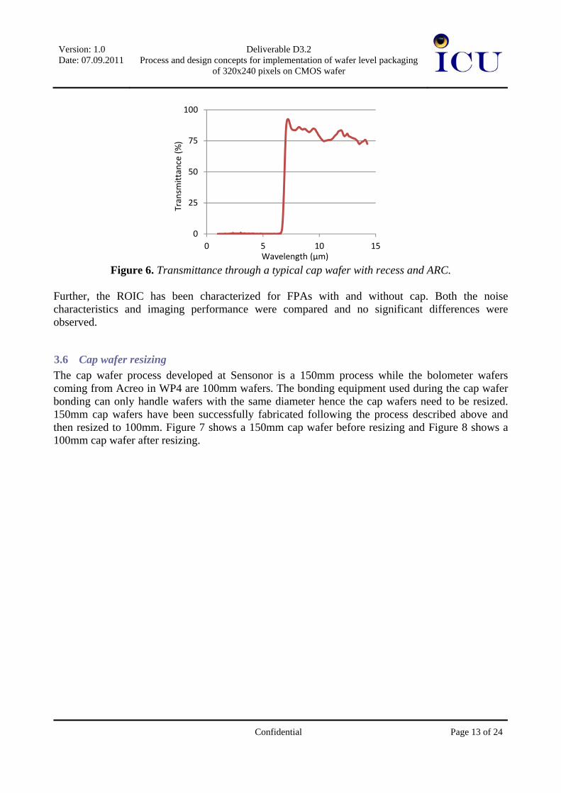
Figure 6 shows the transmittance through a typical cap wafer with recess and ARC from 1µm-14µm. As can be seen the cut on wavelength is around 7µm and the transmittance is high for the relevant wavelengths. The ARC is designed to block shorter wavelengths to avoid excessive heating from solar radiation which would damage the FPA.
Version: 1.0 Date: 07.09.2011
Deliverable D3.2
Process and design concepts for implementation of wafer level packaging of 320x240 pixels on CMOS wafer
Confidential
Page 13 of 24
0
25
50
75
100
0 5 10 15
Tran
smitt
ance
(%)
Wavelength (µm) Figure 6. Transmittance through a typical cap wafer with recess and ARC.
Further, the ROIC has been characterized for FPAs with and without cap. Both the noise characteristics and imaging performance were compared and no significant differences were observed.
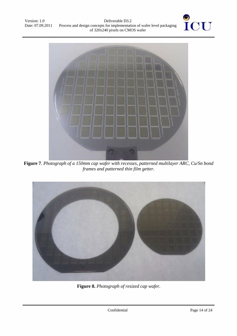
3.6 Cap wafer resizing The cap wafer process developed at Sensonor is a 150mm process while the bolometer wafers coming from Acreo in WP4 are 100mm wafers. The bonding equipment used during the cap wafer bonding can only handle wafers with the same diameter hence the cap wafers need to be resized. 150mm cap wafers have been successfully fabricated following the process described above and then resized to 100mm. Figure 7 shows a 150mm cap wafer before resizing and Figure 8 shows a 100mm cap wafer after resizing.
Version: 1.0 Date: 07.09.2011
Deliverable D3.2
Process and design concepts for implementation of wafer level packaging of 320x240 pixels on CMOS wafer
Confidential
Page 14 of 24
Figure 7. Photograph of a 150mm cap wafer with recesses, patterned multilayer ARC, Cu/Sn bond
frames and patterned thin film getter.
Figure 8. Photograph of resized cap wafer.
Version: 1.0 Date: 07.09.2011
Deliverable D3.2
Process and design concepts for implementation of wafer level packaging of 320x240 pixels on CMOS wafer
Confidential
Page 15 of 24
3.7 Getter definition Figure 9 shows a photograph of a device corner on a cap wafer ready for bonding. The overlay shows the different features on the cap wafer along with nominal dimensions. The areas where the active and blind pixels will be located after cap wafer bonding are also indicated. As can be seen the getter covers the blind pixels with a large overlap and is clearly separated from the active pixels.
Active areaIR transparentGetter not allowed
Bond areaGetter not allowed
Getter(inside recess)
RecessARC(inside recess)
Reference areaNot IR transparentGetter requiredDistance to getter edge >100µm
250µm
1075µm
310µm
300µm
200µm
Figure 9. Photo of a cap wafer prior to bonding. The different features on the wafer are
indicated as well as the positions of the active and blind pixels.
The alignment and definition of the getter are critical parameters for the device performance. The data presented in Table 2 is measured at two chips, i.e. at 3o’clock and 9o’clock with the wafer flat at 6o’clock. The distance to the getter from the bond frames and the width of the getter were measured for all corners of both chips. As can be seen all measured data are within 50µm of the nominal values. Table 2. Measured and nominal dimensions indicating the overlay and definition of the getter. All
values are in µm.
Version: 1.0 Date: 07.09.2011
Deliverable D3.2
Process and design concepts for implementation of wafer level packaging of 320x240 pixels on CMOS wafer
Confidential
Page 16 of 24
Corner x y x y x y
NW 195 95 154 102 200 140
NE 117 97 147 102 140 140
SE 107 147 146 139 140 140
SW 194 147 165 141 200 140
Width of getter SE 743 690 744 699 760 700
Distance to getter from bondframe
Nominal3oclock 9oclock
Since the getter is not IR transparent it is not allowed above the active area. Table 3 presents the data in Table 2 from an active pixel point of view using nominal values to estimate the separation between the getter and the active pixels. It is evident that getter overlapping the active area is not an issue.
Table 3. Estimated and nominal dimensions for the separation between getter and active pixels. The values are estimated from nominal values and values from Table 2. All values are in µm.
Corner x y x y x y
NW - 75 - 59 - 80
NE 215 73 184 59 180 80
SE 225 73 185 72 180 80
SW - 73 - 70 - 80
Nominal
Separation between getter and active area
3oclock 9oclock
Apart from being a critical part in achieving low and stable pressure the getter is also used to block incident IR radiation above the blind pixels, e.g. reference pixels. To avoid diffracted light reaching the blind pixels the overlap should be at least 100µm [1]. Table 4 presents the data in Table 2 from a blind pixel point of view using nominal values to estimate the overlap of the getter over the blind pixels. It is evident that overlap is well above the 100µm limit and hence not an issue. Table 4. Estimated and nominal dimensions for the overlap of the getter over the blind pixels. The overlaps toward the active pixels and bond frame are labeled as yactice and ybondframe respectively.
The values are estimated from nominal values and values from Table 2. All values are in µm.
Corner x yactive ybondframe x yactive ybonframe x yactive ybondframe
NW 325 175 215 366 191 208 380 170 180
NE 958 177 213 928 191 208 875 170 180
SE 968 177 363 929 178 371 875 170 380
SW 326 177 363 355 180 369 380 170 380
9oclock
Overlapping of reference
area
Nominal3oclock
Version: 1.0 Date: 07.09.2011
Deliverable D3.2
Process and design concepts for implementation of wafer level packaging of 320x240 pixels on CMOS wafer
Confidential
Page 17 of 24
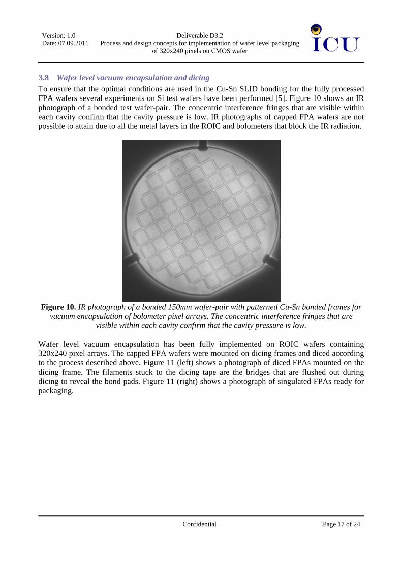
3.8 Wafer level vacuum encapsulation and dicing To ensure that the optimal conditions are used in the Cu-Sn SLID bonding for the fully processed FPA wafers several experiments on Si test wafers have been performed [5]. Figure 10 shows an IR photograph of a bonded test wafer-pair. The concentric interference fringes that are visible within each cavity confirm that the cavity pressure is low. IR photographs of capped FPA wafers are not possible to attain due to all the metal layers in the ROIC and bolometers that block the IR radiation.
Figure 10. IR photograph of a bonded 150mm wafer-pair with patterned Cu-Sn bonded frames for
vacuum encapsulation of bolometer pixel arrays. The concentric interference fringes that are visible within each cavity confirm that the cavity pressure is low.
Wafer level vacuum encapsulation has been fully implemented on ROIC wafers containing 320x240 pixel arrays. The capped FPA wafers were mounted on dicing frames and diced according to the process described above. Figure 11 (left) shows a photograph of diced FPAs mounted on the dicing frame. The filaments stuck to the dicing tape are the bridges that are flushed out during dicing to reveal the bond pads. Figure 11 (right) shows a photograph of singulated FPAs ready for packaging.
Version: 1.0 Date: 07.09.2011
Deliverable D3.2
Process and design concepts for implementation of wafer level packaging of 320x240 pixels on CMOS wafer
Confidential
Page 18 of 24
Figure 11. Photographs of wafer level vacuum encapsulated and diced FPAs mounted on dicing frame The filaments stuck to the dicing tape are the bridges that are flushed out during dicing.
After cap wafer bonding it was possible to see the deflection of the cap wafer due to the low pressure inside the cavity with the naked eye. However, the integrated pressure sensor indicated that the pressure was too high, i.e. >5Pa. Residual gas analyzes (RGA) have been performed to learn more about the composition of the gas inside the cavity.
3.9 Residual gas analysis and Ar outgassing All implementation of wafer level vacuum encapsulation on CMOS wafers with bolometer arrays has to this point been using Sensonor’s 150mm FPA technology [12] due to the delays in WP4. The ICU and the Sensonor FPAs are conceptually identical but they are fabricated in different ways, e.g. different materials, different equipment, etc., and a direct comparison of the RGA results is not relevant at this stage. However, all pre-tests show that the main source of Ar is the ROIC, which is identical for both ICU and Sensonor. The RGAs were performed on two groups of devices. The groups were from the same FPA wafer but were getter activated at two different temperatures. The first group was activated at 350°C while the other was activated at 390°C. The RGA revealed that increasing the getter activation temperature has no significant influence on the amount or composition of the residual gas. No leaky samples were found during the RGA. As expected the main component in the residual gas was found to be Ar but the amount was higher than anticipated. Ar partial pressures of up to 80Pa were observed. Several outgassing experiments have been performed to find the potential Ar sources. Since Ar outgassing from the ROIC is a known problem, two different methods that can be used to reduce it were investigated at an early stage. One was to degas the ROIC at an elevated temperature at some point before cap wafer bonding. Another approach was to coat the ROIC with an Al2O3 diffusion barrier that prevents the Ar from reaching the cavity. The investigated Al2O3 barrier material was deposited by atomic layer deposition which is a deposition method giving very conformal and high quality films.
Kerf
Cap
Cap
Bond pads
Version: 1.0 Date: 07.09.2011
Deliverable D3.2
Process and design concepts for implementation of wafer level packaging of 320x240 pixels on CMOS wafer
Confidential
Page 19 of 24
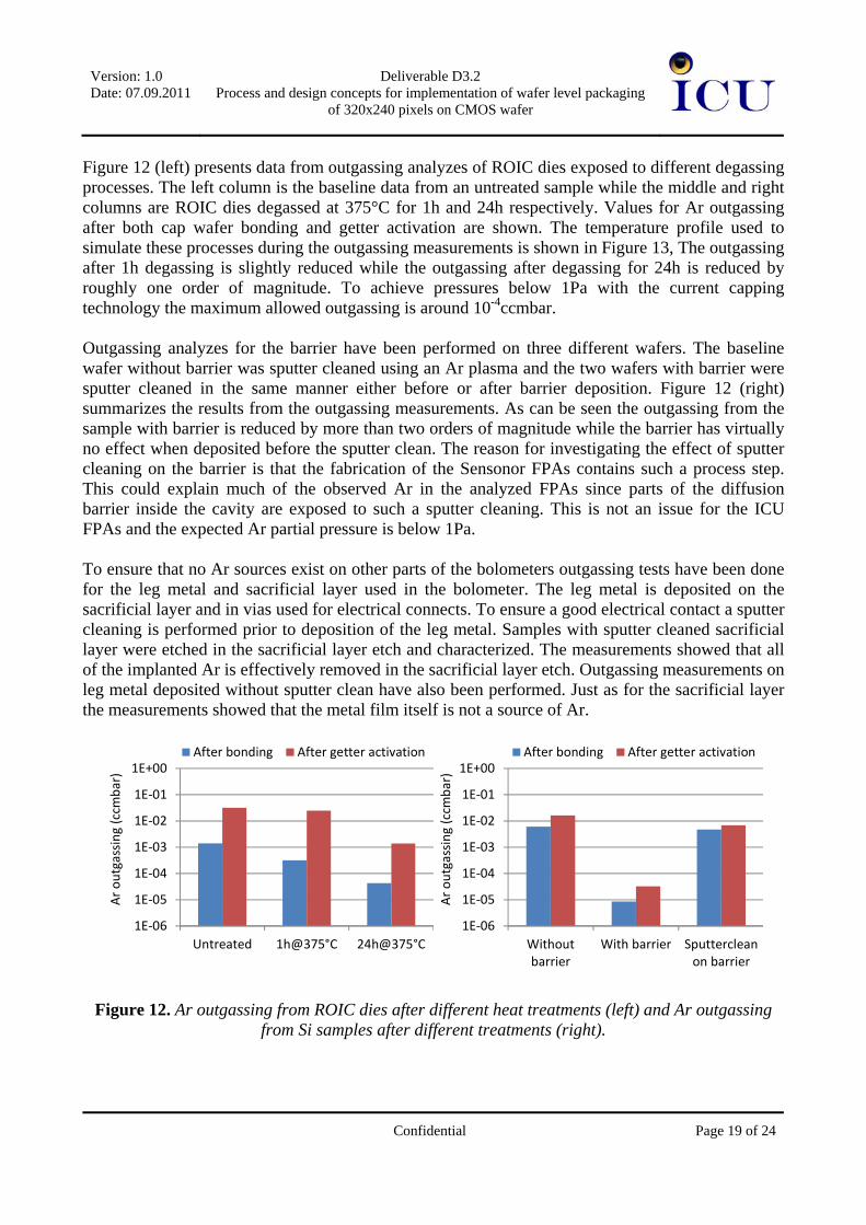
Figure 12 (left) presents data from outgassing analyzes of ROIC dies exposed to different degassing processes. The left column is the baseline data from an untreated sample while the middle and right columns are ROIC dies degassed at 375°C for 1h and 24h respectively. Values for Ar outgassing after both cap wafer bonding and getter activation are shown. The temperature profile used to simulate these processes during the outgassing measurements is shown in Figure 13, The outgassing after 1h degassing is slightly reduced while the outgassing after degassing for 24h is reduced by roughly one order of magnitude. To achieve pressures below 1Pa with the current capping technology the maximum allowed outgassing is around 10-4ccmbar. Outgassing analyzes for the barrier have been performed on three different wafers. The baseline wafer without barrier was sputter cleaned using an Ar plasma and the two wafers with barrier were sputter cleaned in the same manner either before or after barrier deposition. Figure 12 (right) summarizes the results from the outgassing measurements. As can be seen the outgassing from the sample with barrier is reduced by more than two orders of magnitude while the barrier has virtually no effect when deposited before the sputter clean. The reason for investigating the effect of sputter cleaning on the barrier is that the fabrication of the Sensonor FPAs contains such a process step. This could explain much of the observed Ar in the analyzed FPAs since parts of the diffusion barrier inside the cavity are exposed to such a sputter cleaning. This is not an issue for the ICU FPAs and the expected Ar partial pressure is below 1Pa. To ensure that no Ar sources exist on other parts of the bolometers outgassing tests have been done for the leg metal and sacrificial layer used in the bolometer. The leg metal is deposited on the sacrificial layer and in vias used for electrical connects. To ensure a good electrical contact a sputter cleaning is performed prior to deposition of the leg metal. Samples with sputter cleaned sacrificial layer were etched in the sacrificial layer etch and characterized. The measurements showed that all of the implanted Ar is effectively removed in the sacrificial layer etch. Outgassing measurements on leg metal deposited without sputter clean have also been performed. Just as for the sacrificial layer the measurements showed that the metal film itself is not a source of Ar.
1E-06
1E-05
1E-04
1E-03
1E-02
1E-01
1E+00
Untreated 1h@375°C 24h@375°C
Ar
outg
assi
ng (c
cmba
r)
After bonding After getter activation
1E-06
1E-05
1E-04
1E-03
1E-02
1E-01
1E+00
Withoutbarrier
With barrier Sputtercleanon barrier
Ar
outg
assi
ng (c
cmba
r)
After bonding After getter activation
Figure 12. Ar outgassing from ROIC dies after different heat treatments (left) and Ar outgassing
from Si samples after different treatments (right).
Version: 1.0 Date: 07.09.2011
Deliverable D3.2
Process and design concepts for implementation of wafer level packaging of 320x240 pixels on CMOS wafer
Confidential
Page 20 of 24
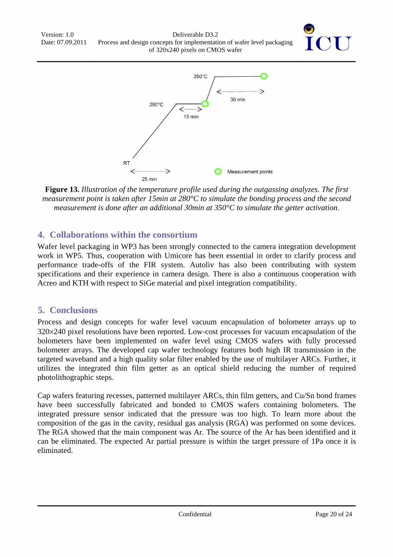
Figure 13. Illustration of the temperature profile used during the outgassing analyzes. The first
measurement point is taken after 15min at 280°C to simulate the bonding process and the second measurement is done after an additional 30min at 350°C to simulate the getter activation.
4. Collaborations within the consortium Wafer level packaging in WP3 has been strongly connected to the camera integration development work in WP5. Thus, cooperation with Umicore has been essential in order to clarify process and performance trade-offs of the FIR system. Autoliv has also been contributing with system specifications and their experience in camera design. There is also a continuous cooperation with Acreo and KTH with respect to SiGe material and pixel integration compatibility.
5. Conclusions Process and design concepts for wafer level vacuum encapsulation of bolometer arrays up to 320×240 pixel resolutions have been reported. Low-cost processes for vacuum encapsulation of the bolometers have been implemented on wafer level using CMOS wafers with fully processed bolometer arrays. The developed cap wafer technology features both high IR transmission in the targeted waveband and a high quality solar filter enabled by the use of multilayer ARCs. Further, it utilizes the integrated thin film getter as an optical shield reducing the number of required photolithographic steps. Cap wafers featuring recesses, patterned multilayer ARCs, thin film getters, and Cu/Sn bond frames have been successfully fabricated and bonded to CMOS wafers containing bolometers. The integrated pressure sensor indicated that the pressure was too high. To learn more about the composition of the gas in the cavity, residual gas analysis (RGA) was performed on some devices. The RGA showed that the main component was Ar. The source of the Ar has been identified and it can be eliminated. The expected Ar partial pressure is within the target pressure of 1Pa once it is eliminated.
Version: 1.0 Date: 07.09.2011
Deliverable D3.2
Process and design concepts for implementation of wafer level packaging of 320x240 pixels on CMOS wafer
Confidential
Page 21 of 24
6. List of references [1] Deliverable report D3.1 in ICU [2] T. Schimert, J. Brady, T. Fagan, M. Taylor, W. McCardel, R. Gooch, S. Ajmera, C. Hanson,
Proceedings of SPIE, Vol.6940, part II, pp.694023-1, 2008. [3] G. Dumont, A. Arnaud, P. Impérinetti, C. Vialle, W. Rabaud, V. Goudon, J-J. Yon,
Proceedings of SPIE, Vol.6940, part II, pp.69401Y-1, 2008. [4] L. Dietrich, G. Engelmann, O. Ehrmann, H. Reichl, “Gold and Gold-Tin Wafer Bumping by
Electrochemical Deposition for Flip Chip and TAB,” 3rd European Conference on Electronic Packaging Technology (EuPac’98), Nuremberg, Germany, June 15-17, 1998.
[5] H. Oppermann, E. Zakel, G. Engelmann, H. Reichl, H.: “Investigation of Self-Alignment
During Flip-Chip Assembly Using Eutectic Gold-Tin Metallurgy”, 4th Int. Conf. and Exhibition on Micro Electro, Opto and Mechanical Systems and Components, MST ‘94.
[6] M. Hutter, H. Oppermann, G. Engelmann, J. Wolf, O. Ehrmann, R. Aschenbrenner, H. Reichl,
“Calculation of Shape and Experimental Creation of AuSn Solder Bumps for Flip Chip Applications,” Proc 52nd Electronic Components and Technology Conf, San Diego, 2002.
[7] H. Huebner, S. Penka, B. Barchmann, M. Eigner, W. Gruber, M. Nobis, S. Janka, G. Kristen,
M. Schneegans, Microelectronic Engineering, Vol. 83, pp.2155 2006 [8] Deliverable report D5.1 in the FNIR project, seventh framework program, GA nr. 216384. [9] Li Li, Jiwei Jiao, Le Luo, Yuelin Wang, Proceedings of the 1st IEEE International Conference
on Nano/Micro Engineered and Molecular Systems, pp.1133, 2006 [10] Deliverable report D5.1 in ICU [11] P.W. Kruse, Uncooled Thermal Imaging. Arrays, Systems, and Applications, SPIE Press,
Bellingham, USA, 2001. [12] Lapadatu, A., Kittilsland, G., Elfving, A., Hohler, E., Kvisterøy, T., Bakke, T., Ericsson, P.,
“High-performance long wave infrared bolometer fabricated by wafer bonding”, Proceedings of SPIE, Vol. 7726, 7726-35 (2010).
Version: 1.0 Date: 07.09.2011
Deliverable D3.2
Process and design concepts for implementation of wafer level packaging of 320x240 pixels on CMOS wafer
Confidential
Page 22 of 24
7. List of Figures
LIST OF FIGURES
FIGURE NO. FIGURE CAPTIONS
Figure 1 Getter design used for the cap wafer. All values are in mm.
Figure 2 Illustration of the process flow for the formation of bond frames on the FPA wafer. a) Etching of openings in sacrificial layer down to ROIC, b) Electro plating of bond frames, and c) Etching of sacrificial layer to release bolometers.
Figure 3 Illustration of the cap wafer process flow. a) Recess etching, b) deposition of ARC, c) Seed layer deposition and electro plating of bond frames with subsequent removal of seed layer, and d) Deposition of getter.
Figure 4 Illustration of temperature and force profiles used during the cap wafer SLID bonding.
Figure 5 Illustration of the process flow for the wafer level vacuum encapsulation. a) Cap wafer SLID bonding, b) Bridge dicing to reveal underlying wire bond pads, c) Dicing, and d) Mount in ceramic package.
Figure 6 Transmittance through a typical cap wafer with recess and ARC.
Figure 7 Photograph of a 150mm cap wafer with recesses, patterned multilayer ARC, Cu/Sn bond frames and patterned thin film getter.
Figure 8 Photograph of resized cap wafer.
Figure 9 Photo of a cap wafer prior to bonding. The different features on the wafer are indicated as well as the positions of the active and blind pixels.
Figure 10 IR photograph of a bonded 150mm wafer-pair with patterned Cu-Sn bonded frames for vacuum encapsulation of bolometer pixel arrays. The concentric interference fringes that are visible within each cavity confirm that the cavity pressure is low.
Figure 11 Photographs of wafer level vacuum encapsulated and diced FPAs mounted on dicing frame The filaments stuck to the dicing tape are the bridges that are flushed out during dicing.
Figure 12 Ar outgassing from ROIC dies after different heat treatments (left) and Ar outgassing from Si samples after different treatments (right).
Figure 13 Illustration of the temperature profile used during the outgassing analyzes. The first measurement point is taken after 15min at 280°C to simulate the bonding process and the second measurement is done after an additional 30min at 350°C to simulate the getter activation.
Version: 1.0 Date: 07.09.2011
Deliverable D3.2
Process and design concepts for implementation of wafer level packaging of 320x240 pixels on CMOS wafer
Confidential
Page 23 of 24
8. List of tables
LIST OF TABLES
TABLE NO. TABLE CAPTIONS
Table 1 Influence on cap wafer IR transmittance from process integration.
Table 2 Measured and nominal dimensions indicating the overlay and definition of the getter. All values are in µm.
Table 3 Estimated and nominal dimensions for the separation between getter and active pixels. The values are estimated from nominal values and values from Table 2. All values are in µm.
Table 4 Estimated and nominal dimensions for the overlap of the getter over the blind pixels. The overlaps toward the active pixels and bond frame are labeled as yactice and ybondframe respectively. The values are estimated from nominal values and values from Table 2. All values are in µm.
Version: 1.0 Date: 07.09.2011
Deliverable D3.2
Process and design concepts for implementation of wafer level packaging of 320x240 pixels on CMOS wafer