This article has been accepted for inclusion in a future issue of this journal. Content is final as presented, with the exception of pagination.
IEEE TRANSACTIONS ON COMPONENTS, PACKAGING AND MANUFACTURING TECHNOLOGY 1
Design, Modeling, Fabrication and Characterizationof 2–5-μm Redistribution Layer Traces by
Advanced Semiadditive Processes on Low-CostPanel-Based Glass Interposers
Hao Lu, Ryuta Furuya, Brett M. D. Sawyer, Chandrasekharan Nair, Fuhan Liu,Venky Sundaram, and Rao R. Tummala, Fellow, IEEE
Abstract— This paper presents the latest advances in extendingsemiadditive process (SAP) methods to 2–5 µm lines and spaces,achieved using dry film photoresists on thin glass substrates,toward meeting the routing requirements for 20-µm bumppitch interposers. High-density chip-to-chip interconnectionson 2.5-D interposers are a key enabler to meet the highlogic to memory bandwidth needs of next-generation electronicsystems. Such 2.5-D interposers require ultrafine redistributionlayer (RDL) traces with line widths and spacing below 5 µm.This paper reports on the extension of panel scale and lowercost SAPs to achieve less than 5 µm lines and spaces, basedon the ultrasmooth surface and improved dimensional stabilityof thin glass panels. A modified low-cost SAP method withnewly developed differential seed layer etching was employedto fabricate the fine line and space patterns and coplanarwaveguide (CPW) transmission on thin glass panels. Fine linesdown to 2-µm lines and spaces and CPW lines with signal lengthsup to 5 mm and ground-to-signal gaps down to 5.5 µm at 15-µmsignal widths were successfully fabricated on ultra-thin glasspanels. For comparison, the same processes were also appliedto a silicon wafer. The signal insertion losses of CPW lineson the glass were 0.024 dB/mm better at 15 GHz than thoseon the silicon, as confirmed by simulations as well as VNAmeasurements. The measured insertion loss of 5-mm long CPWlines on glass interposer was 0.7 dB at 10 GHz and matched wellto the simulated values.
Index Terms— 2.5-D interposer, glass interposer, redistributionlayer (RDL), semiadditive process (SAP).
I. INTRODUCTION
2.5 -D INTERPOSERS integrate logic and memorydevices at close proximity and achieve high
bandwidths by increasing the density of chip-to-chipinterconnections. The 2.5-D architecture has become acompelling alternative to 3-D IC stacking for the scaling of
Manuscript received December 29, 2015; revised March 26, 2016; acceptedApril 3, 2016. Recommended for publication by Associate Editor B. Dangupon evaluation of reviewers’ comments.
Color versions of one or more of the figures in this paper are availableonline at http://ieeexplore.ieee.org.
Digital Object Identifier 10.1109/TCPMT.2016.2556641
smart mobile and cloud computing systems. Traditional 2-Dpackaging of individual devices and connecting them at boardlevel cannot achieve high bandwidths due to the limited pitchscaling of board-level interconnections.
The current approaches for high-density 2.5-D interposersare based on either incrementally extending organic substratesor silicon carriers with through-silicon vias (TSVs), whichutilize back-end of line (BEOL) tools and processes toform multiple redistribution layers (RDLs) at ultrafine pitch.Organic substrates are limited in scaling to fine pitch by thelarge via capture pads due to higher dimensional instabilityand also by lithographic accuracy due to their nonplanarand rough surface. Recent advances in thin-film wiringprocesses have pushed the limits of SAP processes on organicinterposers to less than 10 μm lines and spaces. Kyocera hasdemonstrated 6-μm lines and spaces wiring on low coefficientof thermal expansion (CTE) organic substrates at a 50-μmbump pitch [1]. Organic substrates, however, are ultimatelylimited by their low modulus and high warpage that decreaseschip-level interconnect reliability at decreased bump pitch.To achieve higher wiring density, silicon interposers havebeen developed. Compared with organic substrates, siliconhas excellent dimensional and thermal stability, as well aslow surface roughness for submicrometer wiring. Xilinx useda 65-nm node BEOL processes to demonstrate the first2.5-D silicon interposers with a 45-μm interconnection bumppitch [2], [3]. Shinko has developed a thin-film processtechnology using liquid dielectrics, sputtered metal layer, andchemical–mechanical polish (CMP) processes for fine copperwiring on silicon interposers, to achieve 1.6-μm pitch Cutraces using the SAP method [4]. Shinko also applied siliconwafer processes such as chemical–mechanical polishing andthin film wiring formation to achieve 2-μm lines and spaceson thick organic laminate substrates [5]. The main challengesassociated with such wafer-based interposers are the high costdue to small wafer size (200–300 mm) and RDL fabricationcosts. Silicon interposers also suffer from high electrical signalloss due to the lower resistivity of silicon.
Panel-based glass interposers have been demonstrated asa lower cost and higher performance alternative to address
This article has been accepted for inclusion in a future issue of this journal. Content is final as presented, with the exception of pagination.
2 IEEE TRANSACTIONS ON COMPONENTS, PACKAGING AND MANUFACTURING TECHNOLOGY
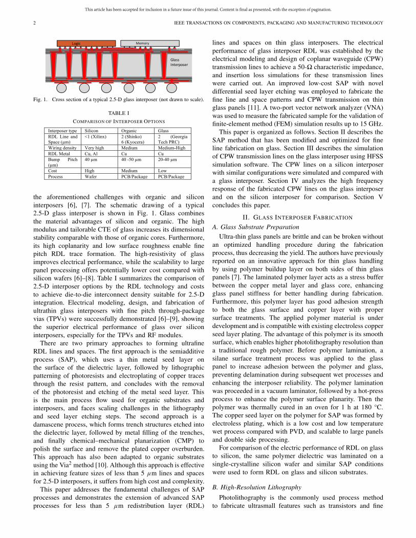
Fig. 1. Cross section of a typical 2.5-D glass interposer (not drawn to scale).
TABLE I
COMPARISON OF INTERPOSER OPTIONS
the aforementioned challenges with organic and siliconinterposers [6], [7]. The schematic drawing of a typical2.5-D glass interposer is shown in Fig. 1. Glass combinesthe material advantages of silicon and organic. The highmodulus and tailorable CTE of glass increases its dimensionalstability comparable with those of organic cores. Furthermore,its high coplanarity and low surface roughness enable finepitch RDL trace formation. The high-resistivity of glassimproves electrical performance, while the scalability to largepanel processing offers potentially lower cost compared withsilicon wafers [6]–[8]. Table I summarizes the comparison of2.5-D interposer options by the RDL technology and coststo achieve die-to-die interconnect density suitable for 2.5-Dintegration. Electrical modeling, design, and fabrication ofultrathin glass interposers with fine pitch through-packagevias (TPVs) were successfully demonstrated [6]–[9], showingthe superior electrical performance of glass over siliconinterposers, especially for the TPVs and RF modules.
There are two primary approaches to forming ultrafineRDL lines and spaces. The first approach is the semiadditiveprocess (SAP), which uses a thin metal seed layer onthe surface of the dielectric layer, followed by lithographicpatterning of photoresists and electroplating of copper tracesthrough the resist pattern, and concludes with the removalof the photoresist and etching of the metal seed layer. Thisis the main process flow used for organic substrates andinterposers, and faces scaling challenges in the lithographyand seed layer etching steps. The second approach is adamascene process, which forms trench structures etched intothe dielectric layer, followed by metal filling of the trenches,and finally chemical–mechanical planarization (CMP) topolish the surface and remove the plated copper overburden.This approach has also been adapted to organic substratesusing the Via2 method [10]. Although this approach is effectivein achieving feature sizes of less than 5 μm lines and spacesfor 2.5-D interposers, it suffers from high cost and complexity.
This paper addresses the fundamental challenges of SAPprocesses and demonstrates the extension of advanced SAPprocesses for less than 5 μm redistribution layer (RDL)
lines and spaces on thin glass interposers. The electricalperformance of glass interposer RDL was established by theelectrical modeling and design of coplanar waveguide (CPW)transmission lines to achieve a 50-� characteristic impedance,and insertion loss simulations for these transmission lineswere carried out. An improved low-cost SAP with noveldifferential seed layer etching was employed to fabricate thefine line and space patterns and CPW transmission on thinglass panels [11]. A two-port vector network analyzer (VNA)was used to measure the fabricated sample for the validation offinite-element method (FEM) simulation results up to 15 GHz.
This paper is organized as follows. Section II describes theSAP method that has been modified and optimized for fineline fabrication on glass. Section III describes the simulationof CPW transmission lines on the glass interposer using HFSSsimulation software. The CPW lines on a silicon interposerwith similar configurations were simulated and compared witha glass interposer. Section IV analyzes the high frequencyresponse of the fabricated CPW lines on the glass interposerand on the silicon interposer for comparison. Section Vconcludes this paper.
II. GLASS INTERPOSER FABRICATION
A. Glass Substrate Preparation
Ultra-thin glass panels are brittle and can be broken withoutan optimized handling procedure during the fabricationprocess, thus decreasing the yield. The authors have previouslyreported on an innovative approach for thin glass handlingby using polymer buildup layer on both sides of thin glasspanels [7]. The laminated polymer layer acts as a stress bufferbetween the copper metal layer and glass core, enhancingglass panel stiffness for better handling during fabrication.Furthermore, this polymer layer has good adhesion strengthto both the glass surface and copper layer with propersurface treatments. The applied polymer material is underdevelopment and is compatible with existing electroless copperseed layer plating. The advantage of this polymer is its smoothsurface, which enables higher photolithography resolution thana traditional rough polymer. Before polymer lamination, asilane surface treatment process was applied to the glasspanel to increase adhesion between the polymer and glass,preventing delamination during subsequent wet processes andenhancing the interposer reliability. The polymer laminationwas proceeded in a vacuum laminator, followed by a hot-pressprocess to enhance the polymer surface planarity. Then thepolymer was thermally cured in an oven for 1 h at 180 °C.The copper seed layer on the polymer for SAP was formed byelectroless plating, which is a low cost and low temperaturewet process compared with PVD, and scalable to large panelsand double side processing.
For comparison of the electric performance of RDL on glassto silicon, the same polymer dielectric was laminated on asingle-crystalline silicon wafer and similar SAP conditionswere used to form RDL on glass and silicon substrates.
B. High-Resolution Lithography
Photolithography is the commonly used process methodto fabricate ultrasmall features such as transistors and fine
This article has been accepted for inclusion in a future issue of this journal. Content is final as presented, with the exception of pagination.
LU et al.: DESIGN, MODELING, FABRICATION, AND CHARACTERIZATION OF 2–5-μm RDL TRACES 3
Fig. 2. High-resolution lithography process flow chart.
line wiring on transistor wafers and on interposers andpackage substrates. Most of the current package substrateprocesses utilize I-line UV lithography in large field sizeexposure mode or in stepper mode for higher resolution butlower throughput. The resolution of the lithography processis one of the key aspects that limit the minimum featuresize of the SAP. This resolution is limited by two typesof factors: 1) photoresist materials, the adhesion strengthof the photoresist to the substrate, and the lithographytools, and 2) substrate properties such as the planarity androughness of the substrate core. A rough and nonplanar surfacewill negatively impact the lithography resolution. Organicsubstrates have larger thickness variation and a rougher surfacecompared with glass substrates, due to the glass fabric woveninside the organic core. Therefore, lithography on glass isexpected to have better yields than on organic substratesat 2–5-μm feature sizes for the same lithography processconditions.
Two forms of photoresist are commonly used forlithography, namely, liquid photoresists, and dry filmresists (DFR). In general, DFRs have lower cost and isbetter suited for double-side processing on large panels thanliquid photoresists. High-resolution DFRs with thickness of7, 10, and 15 μm provided by Hitachi Chemical [12] wereused in this study. To enhance the adhesion between DFRand the copper seed layer surface, an adhesion promotertreatment called Novalink from Atotech was applied. Thissurface treatment process has been proved to significantlyincrease the lithography process yield at the 5-μm featuresize [11], and enables higher lithography resolution below5 μm.
A glass photomask consisting of comb structures, escaperouting structures, and CPW lines was applied in thelithography process. The lithography process flow issummarized in Fig. 2. Fine line patterns with a feature size of2–5 μm were achieved with the appropriate lithography tool,high-resolution DFR, and adhesion promoter treatment.
Ushio’s new advanced projection lithography tool UshioUX-44101 [13] was set up at Georgia Tech PRC. This machinealong with a high-resolution DFR and proper surface treatment
Fig. 3. SEM image of patterned DFR trenches from the 2-μm line and spaceto the 5-μm line and space.
can support the lithography resolution down to 2 μm.The DFR applied in this experiment is 7 μm and the exposuredose is 180 mJ/cm2. The development was done in a spraydeveloping tool with spray nozzles located on both sides of theconveyer. The development chemistry is the sodium carbonatesolution, and the conveyer speed for DFR development was setto 40 inch/min. The SEM image of developed DFR structureswith the 2-μm line and space pattern is shown in Fig. 3. Fig. 3also shows the limitation of the lithography process shownin Fig. 2, as the 1.5 μm trench structure did not yield. For7-μm-thick DFR, the aspect ratio of 1.5-μm line and spacepattern is 4.67, and the stiffness of this DFR is not highenough to support such a high aspect ratio structure. To furtherimprove the lithography resolution, the thickness of the DFRneeds to be reduced or the stiffness needs to be increased.
C. Fine Line Metallization
The copper RDL structures for glass interposer weremetallized by electrolytic plating. The samples were subjectedto a 10-min plasma etching by CF4 and O2 gases with aflow ratio of 1:4, removing any DFR residue in the trenchand improving the wettability of copper surface for betterplating quality. The plating tank chemistry is from Atotech,called Cupracid TP [14]. It contains Electropure copper sulfatesolution, sulfuric acid, sodium chloride, Cupracid TP Leveller,Cupracid Brightener, and Cupracid Starter. To maintain a goodcopper thickness uniformity and smooth surface, the ratio ofinorganic and organic additives in the plating tank needs to becontrolled at an optimal value which Atotech recommended.The copper layer thickness was determined by the electrolyticplating time and current density, which can be calculatedtheoretically using the following equation:
T = Mw I t
2F Aρ
where T is the copper deposit thickness in centimeters, Mwis the copper moler mass (63.546 g/mol), I is the platingcurrent (A), t is the deposit time (s), F is the Faradayconstant (96485.3329 c/mol), A is the area of the deposit incm2, and ρ is the copper density (8.96 g/cm3). The current
This article has been accepted for inclusion in a future issue of this journal. Content is final as presented, with the exception of pagination.
4 IEEE TRANSACTIONS ON COMPONENTS, PACKAGING AND MANUFACTURING TECHNOLOGY
Fig. 4. Standard immersion seed layer wet etching. Etching speedindependent of direction and copper type.
applied for fine line metallization was 1.5 or 0.015 A/cm2,which is I/A in the above equation. It is worth noting that inpractice, the deposited copper thickness is around 75%–80%of the theoretical value or even lower. A stripping solventwas used to remove the DFR following the electrolytic copperplating process.
The copper seed layer etching was the last step to obtain thedesigned one metal layer RDL patterns. This critical processdetermines the limitation and the yield of the SAP methodfor the fine line RDL. The standard immersion wet etchingprocess is isotropic, which is not ideal for the fine line SAP,as depicted in Fig. 4. For a single line structure, the coppertrace side wall and top are etched at the same rate as the seedlayer, resulting in narrower and lower line profiles as wellas undercut. In practice, particularly for 2.5-D interposers,high-density multiline structures are required. For line andspace patterns below 8 μm, the ability of the etching solutionto penetrate the narrow and high aspect ratio trenches betweencopper traces becomes a challenging aspect. As a result, theetching speed of the copper traces is faster than the seed layer,causing over etch and undercut of copper traces. This leadsto trapezoidal shaped lines, rough copper surface, and evendelamination of ultrafine copper traces. Therefore, this etchingmethod is suitable for large copper patterns, but not for fineline interposer fabrication.
A seed layer etching process with adequate selectivity isrequired to fabricate 2 μm features and enable line densitiesrequired for 2.5-D integration. A spray etching methodincreases the selectivity of etching direction, causing highervertical etching speed than lateral etching speed (Fig. 5).Similar to the immersion seed layer etching process, thecopper surface is attacked by the etchant, resulting in a
Fig. 6. Spray etching with differential etchants. Etching speed dependent ondirection and copper type.
Fig. 7. Cross-sectional image of the 5 μm line and space pattern afterimmerge seed layer etching (top) and differential etching (bottom).
rough copper surface. To further improve the anisotropy ofthe seed layer etching process, differential etchant chemistrieshave been developed by Atotech called CupraEtch DE [15].Such chemistries have special additives that passivate theelectroplated copper sidewall during etching, and also createa differential etch rate with the copper seed layer etching attwice the rate of the electrolytic plated copper, driven by thedifferent grain structures. This etchant also yields smoothercopper surfaces after seed layer removal. By combining thespray etching method with the differential etchant, a novelhigh selectivity etching approach was developed for fine lineRDL fabrication as shown in Fig. 6.
All three different etching methods were tested andcompared. Fig. 7 shows the 5 μm line and space pattern afterimmersion seed layer etching and Atotech differential etching.The copper traces were badly deformed after immersion seedlayer etching. Using differential etching, however, the lineshape integrity was improved. Fig. 8 shows the comparisonbetween the two copper etchants. The copper surface becamerougher and matte after applying a standard copper etchant,but the differential etchant was capable of yielding a shiny andsmooth copper surface due to the increased etched selectivitybetween electroless and electrolytic plated copper.
For the glass interposer fabrication, the differential etchmethod was selected and optimized to obtain high quality RDLtraces with improved yield. Fig. 9 shows the escape routingtest pattern with 5 μm line and space on glass interposer beforeseed layer etching and after DFR strip, and Fig. 10 shows thesame structure after differential seed layer etching. No seedlayer residue is observed from the image, and the etchingprocess did not deform or alter the line shape significantly.Following SAP, open/short tests of this escape routing patternconfirmed that the improved seed layer etch process resulted
This article has been accepted for inclusion in a future issue of this journal. Content is final as presented, with the exception of pagination.
LU et al.: DESIGN, MODELING, FABRICATION, AND CHARACTERIZATION OF 2–5-μm RDL TRACES 5
Fig. 8. CPW transmission line on the glass interposer etched by standardspray etch (top) and differential etch (bottom).
Fig. 9. Optical microscope and SEM image of the 5-μm line and spaceescape routing test patterns before copper seed layer etching.
in no seed layer residues. Test structures with 2 μm lineand space escape routing patterns at 40 μm pad pitch werealso fabricated on glass substrates using the same process, asshown in Fig. 11. Optical inspection of this structure revealedapproximately 0.5 μm side wall etch, resulting in 1 μmline width reduction. This demonstrates the limitation of etchselectivity of the improved SAP process at 2 μm line and spaceand must be considered during interposer design to improveprocess yield. The actual line and space for 2 μm designedpattern was 0.8 μm line and 3.2 μm space. (Fig. 11) The causeof the side wall is discussed in the following paragraph.
Optimizing electroless copper plating and seed layer etchconditions can improve fine line yield using the proposed
Fig. 10. Optical microscope and SEM image of the 5-μm line and spaceescape routing test patterns after copper seed layer etching.
Fig. 11. SEM image of the 3-μm line and space (top) and the 2-μm lineand space (bottom) escape routing patterns at a 40-μm pad pitch.
Fig. 12. AFM image of dielectric polymer surface before (left) andafter (right) desmear process.
SAP method. The copper seed layer was electroless platedon the polymer surface. Strong adhesion is required to ensurethat the fine copper traces do not delaminate from the polymer.Therefore, a desmear process was applied on the polymer
This article has been accepted for inclusion in a future issue of this journal. Content is final as presented, with the exception of pagination.
6 IEEE TRANSACTIONS ON COMPONENTS, PACKAGING AND MANUFACTURING TECHNOLOGY
Fig. 13. Copper traces side wall etch due to roughened polymer surface.
surface before electroless copper plating. This process etchesthe polymer surface, increasing the surface roughness. Thus,the copper seed layer can be anchored on the polymer surfacewith strong mechanical adhesion and electrolytic plated finecopper traces do not delaminate after seed layer etch process.The surface roughness of polymer before and after desmearprocess is shown in Fig. 12. The increased Rz , however, iscritical for the copper seed layer etch process. The copper seedon larger Rz surface has stronger adhesion but suffers from arelatively lower copper etch rate. The seed layer etch on theroughened polymer surface is shown in Fig. 13. The initialseed layer etch rate is fast and independent of the polymerroughness. However, it is difficult to fully etch the copperseed layer residue that is embedded in the rough polymersubsurface, thus requiring extended etching times. This causesa decrease in the overall seed layer etch rate and increases theamount of copper trace side wall lateral etch, resulting in loweryield of the fine copper traces. Therefore, proper optimizationof copper to polymer adhesion using desmear and mask designcompensation are needed to improve fine line yield.
III. ELECTRICAL SIMULATION OF RDL TRACES FOR
GLASS AND SILICON INTERPOSER
This section describes the electrical modeling of CPWtest structures as RDL traces for glass interposers andsilicon interposer for comparison. For minimum insertionloss, the transmission lines were designed to achieve a 50-�characteristic impedance. Ansoft HFSS, a 3-D FEM solverfor electromagnetic structures, was used to simulate thetransmission lines on glass and silicon interposers.
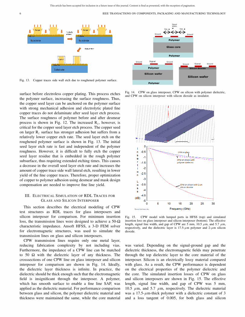
CPW transmission lines require only one metal layer,reducing fabrication complexity by not including vias.Furthermore, the impedance of a CPW line can be matchedto 50 � with the dielectric layer of any thickness. Thecrosssections of one CPW line on glass interposer and siliconinterposer for comparison are shown in Fig. 14. Ideally,the dielectric layer thickness is infinite. In practice, thedielectric should be thick enough such that the electromagneticfield is insignificant through the interposer. A polymer,which has smooth surface to enable a fine line SAP, wasapplied as the dielectric material. For performance comparisonbetween glass and silicon, the polymer dielectric material andthickness were maintained the same, while the core material
Fig. 14. CPW on glass interposer, CPW on silicon with polymer dielectric,and CPW on silicon interposer with silicon dioxide as insulator.
Fig. 15. CPW model with lumped ports in HFSS (top) and simulatedinsertion loss on glass interposer and silicon interposer (bottom). The effectivelength, signal line width, and gap of CPW are 5 mm, 10.5 μm, and 5.7 μm,respectively, and the dielectric layer is 17.5-μm polymer and 2-μm silicondioxide.
was varied. Depending on the signal-ground gap and thedielectric thickness, the electromagnetic fields may penetratethrough the top dielectric layer to the core material of theinterposer. Silicon is an electrically lossy material comparedwith glass. As a result, the CPW performance is dependenton the electrical properties of the polymer dielectric andthe core. The simulated insertion losses of CPW on glassand silicon interposers are shown in Fig. 15. The effectivelength, signal line width, and gap of CPW was 5 mm,10.5 μm, and 5.7 μm, respectively. The dielectric materialwas a 17.5-μm-thick polymer with a dielectric constant of 3and a loss tangent of 0.005, for both glass and silicon
This article has been accepted for inclusion in a future issue of this journal. Content is final as presented, with the exception of pagination.
LU et al.: DESIGN, MODELING, FABRICATION, AND CHARACTERIZATION OF 2–5-μm RDL TRACES 7
Fig. 16. Cross-sectional image of VNA measured CPW line (top) andthe cross-sectional image of the modified CPW model in HFSS with waveports (bottom).
substrate, and 2-μm-thick silicon dioxide for the traditionalsilicon interposer. The dielectric constant of the glass substratewas 5.3, and the silicon substrate had a dielectric constantof 11.9, with an electrical conductivity of 10 S/m. To matchthe CPW characteristic impedance to 50 �, the thicknessof the copper was adjusted for different configurations. TheCPW on the traditional silicon interposer is thinner than onglass interposer because of the high dielectric constant ofsilicon. The simulation results showed that the insertion lossof CPW traces on the polymer laminated silicon interposerwas higher than on glass interposer, and the thinner CPW onthe traditional silicon interposer has much higher insertion lossthan the other two. This is consistent with the fact that siliconhas higher electrical loss than glass. The higher conductivity ofsilicon causes the observed higher loss of the electromagneticwave energy in the simulation results.
IV. ELECTRICAL CHARACTERIZATION OF RDL TRACES
ON GLASS AND SILICON INTERPOSER
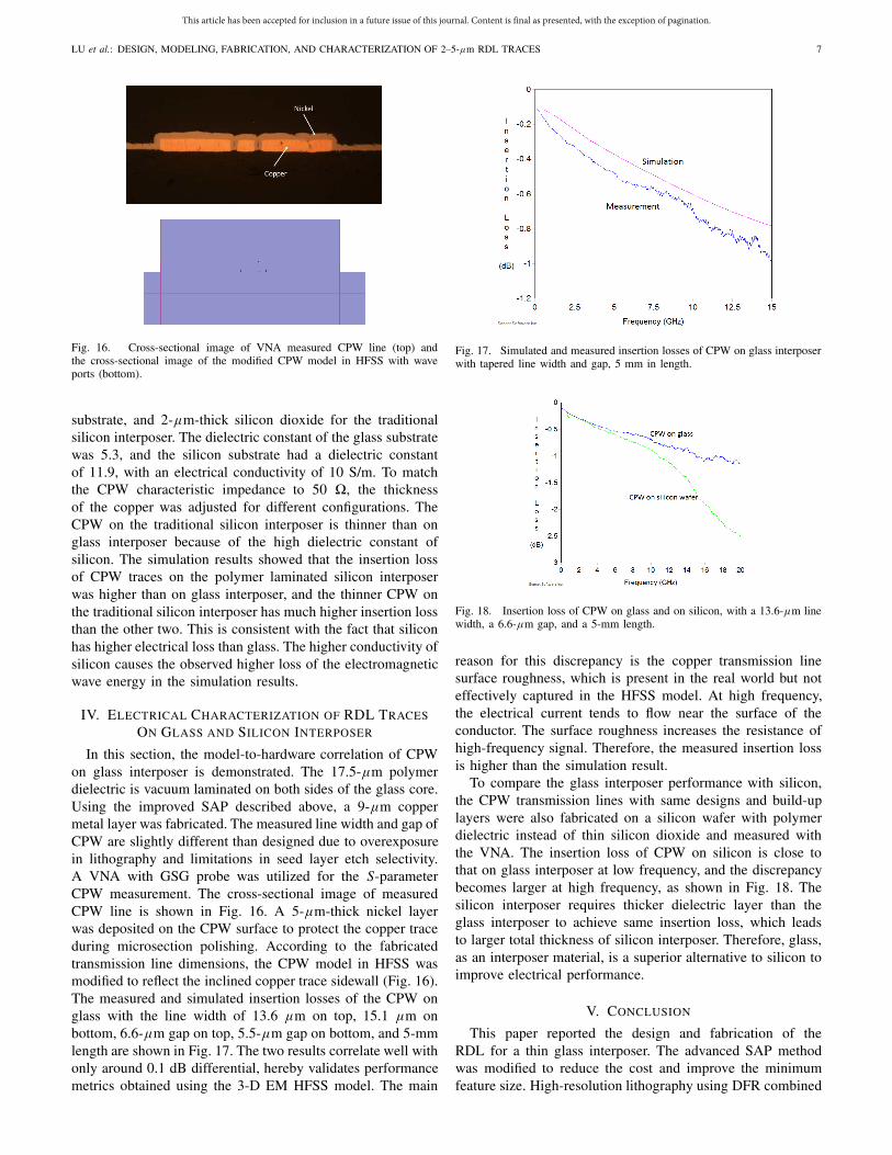
In this section, the model-to-hardware correlation of CPWon glass interposer is demonstrated. The 17.5-μm polymerdielectric is vacuum laminated on both sides of the glass core.Using the improved SAP described above, a 9-μm coppermetal layer was fabricated. The measured line width and gap ofCPW are slightly different than designed due to overexposurein lithography and limitations in seed layer etch selectivity.A VNA with GSG probe was utilized for the S-parameterCPW measurement. The cross-sectional image of measuredCPW line is shown in Fig. 16. A 5-μm-thick nickel layerwas deposited on the CPW surface to protect the copper traceduring microsection polishing. According to the fabricatedtransmission line dimensions, the CPW model in HFSS wasmodified to reflect the inclined copper trace sidewall (Fig. 16).The measured and simulated insertion losses of the CPW onglass with the line width of 13.6 μm on top, 15.1 μm onbottom, 6.6-μm gap on top, 5.5-μm gap on bottom, and 5-mmlength are shown in Fig. 17. The two results correlate well withonly around 0.1 dB differential, hereby validates performancemetrics obtained using the 3-D EM HFSS model. The main
Fig. 17. Simulated and measured insertion losses of CPW on glass interposerwith tapered line width and gap, 5 mm in length.
Fig. 18. Insertion loss of CPW on glass and on silicon, with a 13.6-μm linewidth, a 6.6-μm gap, and a 5-mm length.
reason for this discrepancy is the copper transmission linesurface roughness, which is present in the real world but noteffectively captured in the HFSS model. At high frequency,the electrical current tends to flow near the surface of theconductor. The surface roughness increases the resistance ofhigh-frequency signal. Therefore, the measured insertion lossis higher than the simulation result.
To compare the glass interposer performance with silicon,the CPW transmission lines with same designs and build-uplayers were also fabricated on a silicon wafer with polymerdielectric instead of thin silicon dioxide and measured withthe VNA. The insertion loss of CPW on silicon is close tothat on glass interposer at low frequency, and the discrepancybecomes larger at high frequency, as shown in Fig. 18. Thesilicon interposer requires thicker dielectric layer than theglass interposer to achieve same insertion loss, which leadsto larger total thickness of silicon interposer. Therefore, glass,as an interposer material, is a superior alternative to silicon toimprove electrical performance.
V. CONCLUSION
This paper reported the design and fabrication of theRDL for a thin glass interposer. The advanced SAP methodwas modified to reduce the cost and improve the minimumfeature size. High-resolution lithography using DFR combined
This article has been accepted for inclusion in a future issue of this journal. Content is final as presented, with the exception of pagination.
8 IEEE TRANSACTIONS ON COMPONENTS, PACKAGING AND MANUFACTURING TECHNOLOGY
with differential copper seed layer etching advances thelimit of SAP method to 2 μm while maintaining low cost.Assisted by a novel differential seed layer etching method,this advanced SAP for panel-based ultrathin glass interposerfabrication has a great potential for low-cost applicationsthat require high I/O density comparable to conventionalsilicon interposers with wafer-level process. The simulatedCPW line frequency response in HFSS shows that theelectrical performance of the glass interposer has lowerinsertion loss compared with that of the silicon interposer.This was validated by the VNA measurement up to 20 GHz.Further improvements to the SAP process on glass as wellas multilayer RDL processes with ultrafine wiring for 2.5-Dglass interposer packages will be reported in the future.
REFERENCES
[1] M. Ishida, “APX (advanced package X)—Advanced organic technologyfor 2.5D interposer,” in Proc. CPMT Seminar, Latest Adv. OrganicInterposers (ECTC), Lake Buena Vista, FL, USA, May 2014. [Online].Available: https://www.ectc.net/files/64/5%20Thursday%20PM%20Orga-nic%20Substrates%20Session/4%20CPMT%20Seminar%20140529%20M.%20Ishida,%20Kyocera%20WEB%20UP.pdf
[2] P. Dorsey, “Xilinx stacked silicon interconnect technology deliversbreakthrough FPGA capacity, bandwidth, and power efficiency,” Xilinx,San Jose, CA, USA, White Paper Virtex-7 FPGAs, WP380 (v1.2),Dec. 2012.
[3] B. Banijamali, S. Ramalingam, H. Liu, and M. Kim, “Outstanding andinnovative reliability study of 3D TSV interposer and fine pitch soldermicro-bumps,” in Proc. 62nd Electron. Compon. Technol. Conf. (ECTC),May/Jun. 2012, pp. 309–314.
[4] M. Sunohara, A. Shiraishi, Y. Taguchi, K. Murayama, M. Higashi, andM. Shimizu, “Development of silicon module with TSVs and globalwiring (L/S = 0.8/0.8 μm),” in Proc. 59th Electron. Compon. Technol.Conf., May 2009, pp. 25–31.
[5] K. Oi et al., “Development of new 2.5D package with novel integratedorganic interposer substrate with ultra-fine wiring and high densitybumps,” in Proc. IEEE 64th Electron. Compon. Technol. Conf.,May 2014, pp. 348–353.
[6] V. Sukumaran et al., “Through-package-via formation and metallizationof glass interposers,” in Proc. 61st Electron. Compon. Technol.Conf. (ECTC), Jun. 2011, pp. 557–563.
[7] V. Sukumaran, T. Bandyopadhyay, V. Sundaram, and R. Tummala,“Low-cost thin glass interposers as a superior alternative to silicon andorganic interposers for packaging of 3-D ICs,” IEEE Trans. Compon.,Packag., Manuf. Technol., vol. 2, no. 9, pp. 1426–1433, Sep. 2012.
[8] V. Sridharan et al., “Design and fabrication of bandpass filters in glassinterposer with through-package-vias (TPV),” in Proc. 60th Electron.Compon. Technol. Conf. (ECTC), Jun. 2010, pp. 530–535.
[9] V. Sukumaran et al., “Design, fabrication and characterizationof low-cost glass interposers with fine-pitch through-package-vias,”in Proc. IEEE 61st Electron. Compon. Technol. Conf. (ECTC),May/Jun. 2011, pp. 583–588.
[10] Atotech Inc. Via2 Technology—Copper Trench Filling for Ultra FineLines. accessed on 2015. [Online]. Available: http://www.atotech.com/products/electronics/panel-pattern-plating/horizontal-systems/via2-technology.html
[11] H. Lu et al., “Demonstration of 3–5 μm RDL line lithography onpanel-based glass interposers,” in Proc. IEEE 64th Electron. Compon.Technol. Conf., May 2014, pp. 1416–1420.
[12] Hitachi Chemical Co., Ltd. (2013). RY Series for PKG Board. [Online].Available: http://www.hitachi-chem.co.jp/english/products/pm/017.html
[13] USHIO Inc. (2013). Lighting Edge Technologies. [Online]. Available:http://www.ushio.co.jp/en/index.html
[14] Atotech Inc. (2004). Cupracid TP, accessed on 2004. [Online].Available: http://www.atotech.com/products/electronics/panel-pattern-plating/vertical-systems/dc-plating-with-soluble-anodes.html
[15] N. Lützow, G. Schmidt, Ö. Erdogan, and W. Wong, “CupraEtchDE—Recyclable anisotropic etchant for advanced flip chipmanufacturing,” in Proc. 7th Int. Microsyst., Packag., Assembly CircuitsTechnol. Conf. (IMPACT), 2012, pp. 110–113. [Online]. Available: http://www.atotech.com/fileadmin/pdf/papers/el/CupraEtch-DE_Recyclable_anisotropic_Etchant_for_Advanced_Flip_Chip_Manufacturing.pdf
Hao Lu received the B.S. and M.S. degreesin mechanical engineering from the HuazhongUniversity of Science and Technology, Wuhan,China. He is currently pursuing the Ph.D. degreewith the School of Electrical and ComputerEngineering, Georgia Institute of Technology(Georgia Tech), Atlanta, GA, USA.
He is also a Graduate Research Assistant with the3-D Systems Packaging Research Center, GeorgiaTech. His current research interests include themultilayer redistribution layer design, fabrication,
and signal integrity analysis for cost driven panel-based glass interposer.
Ryuta Furuya received the B.S. and M.S. degreesin physics from the University of Tokyo, Tokyo,Japan, in 2010 and 2012, respectively.
He joined USHIO Inc., Tokyo, Japan, in 2012.He is currently with the 3-D Packaging ResearchCenter, Georgia Institute of Technology, Atlanta,GA, USA, as a Visiting Engineer. His recent researchis the development of high density panel-based2.5-D glass interposer and photonic package. Hiscurrent research interests include functional device,energy harvesting, and microelectromechanical
systems package.
Brett M. D. Sawyer received the B.S. degreein electrical engineering from Old DominionUniversity, Norfolk, VA, USA, in 2011, and theM.S. degree in electrical engineering from theGeorgia Institute of Technology (Georgia Tech),Atlanta, GA, USA, in 2014, where he is currentlypursuing the Ph.D. degree in electrical engineering.
He joined the 3-D Systems Packaging ResearchCenter, Georgia Tech, in 2013. His current researchinterests include the design and demonstration ofa 2.5-D glass interposer package to achieve Tb/s
die-to-die and 400 Gb/s off-interposer bandwidths.
Chandrasekharan Nair received the bachelor’sdegree in polymer engineering and technology witha minor in chemical engineering from the Instituteof Chemical Technology, Mumbai, India, in 2013.He is currently pursuing the Ph.D. degree inmaterials science and engineering with the 3-DPackaging Research Center, Georgia Institute ofTechnology, Atlanta, GA, USA, under the guidanceof Prof. R. Tummala.
His recent research is the reliability evaluation ofnovel polymer dielectric materials and processes to
build next generation redistribution layer for panel scale interposers/highdensity packages as a Graduate Research Assistant in the Low Cost GlassInterposer Program. His current research interests include polymer-metalinterfaces, package substrate reliability studies, and polymer characterization.
This article has been accepted for inclusion in a future issue of this journal. Content is final as presented, with the exception of pagination.
LU et al.: DESIGN, MODELING, FABRICATION, AND CHARACTERIZATION OF 2–5-μm RDL TRACES 9
Fuhan Liu Graduated from the Department ofPhysics, Fudan University, Shanghai, China.
He is currently a Program Manager of 3-DGlass Photonics and Next Generation RedistributionLayer (RDL) with the 3-D Systems PackagingResearch Center, Georgia Institute of Technology,Atlanta, GA, USA. He is focused on research anddevelopment of system-on-package, integration ofhigh density and high speed optoelectronics, singlemode/multimode fiber to waveguide and photonicIC integration, ultrahigh-density RDL with extended
semi-additive process, and embedded trench approaches. He has developed anovel via-in-trench RDL configuration with 2/2/2/20 μm (line/space/via/pitch)on thin glass panel for 20–40 μm ultrafine pitch 2.5-D interposers and fan-outpackages. He developed and demonstrated 1-2 layer ultralow cost thin organicpackage for I/Os >500 flip chip, chip-last embedded ICs in high performanceorganic package for 1–110 GHz multiband applications, 10–40 GB high speedoptical interconnect integration systems, and multispectral imaging CMOSimager with mosaic filter for bioapplication. He has been involved in thepackaging research for more than 20 years. He has authored or co-authoredover 100 papers.
Venky Sundaram received the B.S. degree fromIIT Mumbai, Mumbai, India, and the M.S. andPh.D. degrees in materials science and engineeringfrom the Georgia Institute of Technology (GeorgiaTech), Atlanta, GA, USA.
He is currently the Director of Research andIndustry Relations with the 3-D Systems PackagingResearch Center, Georgia Tech. He is the ProgramDirector of the Low-Cost Interposer and PackagesIndustry Consortium with over 25 active globalindustry members. He is a Globally Recognized
Expert in packaging technology, and the Co-Founder of Jacket MicroDevices, Livonia, MI, USA, and a RF/wireless startup acquired by AVXCorporation, Fountain Inn, SC, USA. He has authored over 100 publicationsand holds 15 patents. His current research interests include system-on-packagetechnology, 3-D packaging and integration, ultrahigh-density interposers,embedded components, and systems integration research.
Dr. Sundaram has received several best paper awards. He is the Co-Chairmanof the IEEE Components, Packaging and Manufacturing Technology TechnicalCommittee on High Density Substrates and the Director of EducationPrograms with the Executive Council of the International Microelectronicsand Packaging Society.
Rao R. Tummala (F’93) received the B.S. degreefrom the Indian Institute of Science (IIS), Bangalore,India, and the Ph.D. degree from the Universityof Illinois at Urbana–Champaign, Champaign,IL, USA.
He was an IBM Fellow, pioneering the first plasmadisplay and multichip electronics for mainframesand servers. He is currently a Distinguished andEndowed Chair Professor and the Founding Directorof the National Science Foundation’s EngineeringResearch Center with the Georgia Institute of
Technology (Georgia Tech), Atlanta, GA, USA, pioneering Moore’s lawfor system integration. He has authored over 500 technical papers, thefirst modern book entitled Microelectronics Packaging Handbook, the firstundergrad textbook entitled Fundamentals of Microsystems Packaging, and thefirst book introducing the system-on-package technology, and holds 74 patentsand inventions.
Prof. Tummala is a member of the National Academy of Engineering.He has received many industry, academic, and professional society awards,including the Industry Week’s Award for improving the U.S. competitiveness,the IEEE David Sarnoff and Dan Hughes Awards from the InternationalMicroelectronics and Packaging Society, the Engineering Materials Awardfrom ASM, and the Total Excellence in Manufacturing Award from theSociety of Manufacturing Engineers. He was a recipient of the DistinguishedAlumni Awards from the University of Illinois at Urbana–Champaign, IIS, andGeorgia Tech, the Technovisionary Award from the Indian SemiconductorAssociation, and the IEEE Field Award for his contributions in electronicssystems integration and cross-disciplinary education in 2011. He was thePresident of the IEEE Components, Packaging and Manufacturing Technologyand the International Microelectronics and Packaging Society.