IEEE TRANSACTIONS ON MICROWAVE THEORY AND TECHNIQUES, VOL. 64, NO. 11, NOVEMBER 2016 4063
Wideband Conducted Electromagnetic EmissionMeasurements Using IPD Chip Probes
Yin-Cheng Chang, Ping-Yi Wang, Da-Chiang Chang, and Shawn S. H. Hsu, Member, IEEE
Abstract— A novel on-chip measurement technique for charac-terizing conducted electromagnetic emission of integrated circuitsin the gigahertz frequency range is proposed. The InternationalElectrotechnical Commission (IEC) direct coupling method isreviewed, and the considerations on improving the applicablebandwidth of the testing probes are discussed. Design of themost critical resistive components for the probes is elaborated toachieve the required accuracy and bandwidth. With the compactchip probes realized by the integrated passive device (IPD)technology, the measurement bandwidth can be significantlyextended compared with the conventionally used surface mounteddevice resistors. The probes are verified to comply with the IEC61967-4 standard, and an excellent bandwidth up to 15 GHzcan be achieved. By connecting the flipped die under test withthe probes embedded in IPD substrate (core sizes of the 1-�current probe and 150-� voltage probe are 0.55 mm × 0.77 mmand 0.83 mm × 1.49 mm, respectively), the conducted emissionmeasurement of a 58-MHz oscillator integrated circuit is demon-strated up to 3 GHz.
Index Terms— 1-/150-� probe, conducted electromag-netic (EM) emission, EM compatibility (EMC), integratedpassive device (IPD), on-chip measurements.
I. INTRODUCTION
ELECTROMAGNETIC compatibility (EMC) becomes anincreasingly important issue for integrated circuits (ICs)
owing to the rapid scaling of transistor feature size with ahigh integration level. The advanced technology allows ICs toachieve high-speed performance under low power dissipation.However, the circuits also generate more noise and becomemore vulnerable to interference. As a result, understanding andcharacterizing the behaviors of electromagnetic (EM) emis-sion and immunity of ICs, especially at increased operatingfrequencies, become a crucial topic for system integration.
A set of IC level test methods on EM interference [Interna-tional Electrotechnical Commission (IEC) 61967] [1] and EMsusceptibility (IEC 62132) [2] was released by the technologysubcommittee 47A of IEC to investigate EMC problems.Depending on the transfer types of EM wave, the test methods
Manuscript received April 30, 2016; revised July 18, 2016 andAugust 29, 2016; accepted August 31, 2016. Date of publicationSeptember 22, 2016; date of current version November 3, 2016. This workwas supported under Contract MOST 103-2221-E-007-115-MY3.
Y.-C. Chang, P.-Y. Wang, and S. S. H. Hsu are with the Department ofElectrical Engineering, National Tsing Hua University, Hsinchu 300, Taiwan(e-mail: [email protected]).
D.-C. Chang is with the National Chip Implementation Center,National Applied Research Laboratories, Hsinchu 300, Taiwan (e-mail:[email protected]).
Color versions of one or more of the figures in this paper are availableonline at http://ieeexplore.ieee.org.
Digital Object Identifier 10.1109/TMTT.2016.2606387
can be classified into radiated or conducted ones. Investigationof the EM emission issue mainly relies on the measurementsowing to the complexity of analytical equations and modeling.The radiated emission measurements typically used include thetransverse EM (TEM) cell method [3]–[5] and the surface scanmethod [6], [7]. With the advantage of contactless nature, theTEM cell utilizes the shielded enclosure to receive the coupledsignal from a device under test (DUT). On the other hand, thesurface scan method relies on the electric (E)/magnetic (H)probes to evaluate the near-field E/H components at thesurface of the DUT. Compared with the radiated measurementapproach, the conducted method allows the physical linkbetween probes and the DUT to guarantee the results withbetter repeatability and correlation [8], [9].
The ICEM model [10] is considered to be relatively accuratefor describing the EMC behavior of ICs. Built from bothsimulated and measured results, the ICEM is composed oftwo main macromodels including the internal activity (IA)and power distribution network (PDN). The IA is consideredas the source of noise, whereas the PDN represents thetransmission media. The PDN modeling techniques are quitemature nowadays, while modeling of IA remains challenging.In general, the IA modeling by transistor level simulation is notpractical due to tedious data processing. The most commonlyused solution for IA modeling is to convert the measuredwaveform back to an equivalent noise current source. Thisblack box approach uses piecewise linear description to serveas the current generator in the simulator directly [11]. Someworks also use the transfer function of testing facility withthe known PDN to obtain an equivalent current source fromthe measured data in either frequency or time domain [12].As can be seen, measurements play an essential role inthe characterization and modeling of the EM emissionbehavior.
With the EM emission caused by the fast changes ofcurrents/voltages in the ICs, the resulting interference in theradio frequency (RF) range could distribute via the on-chippassive PDN, interconnection of package (solder bump, bondwire, and IC pins), and the off-chip PDN (traces on PCB andcable harness). The EMC strategies [13]–[15] are essential tosuppress the noise and ensure the reliability of the circuit andsystem operation. The measurements using the 1-� currentprobe and 150-� voltage probe are standardized asIEC 61967-4 [16], as known as the direct coupling method toinvestigate the conducted EM emission in the RF range. Usingprobes typically built by lumped components with PCB, theEM emission characteristics of ICs can be observed.
4064 IEEE TRANSACTIONS ON MICROWAVE THEORY AND TECHNIQUES, VOL. 64, NO. 11, NOVEMBER 2016
The direct coupling method is concise and popular amongvarious testing techniques of EM emission. Although accuracyconcern of the 150-� method was reported with some com-parative experiments [17], [18] in the early period, the issuehas been improved and this method is widely used nowadays.In contrast, even with the details depicted in the standard, veryfew works were reported based on the measurement methodwith the 1-� current probe [19], [20]. The main challengeis to meet the specifications of the 1-� current probe inpractice [21]. It should be emphasized that the specification ofthe 1-� current probe in most of the published papers was notverified, which may lead to a measurement error, especially athigh frequencies.
Most released standards such as the IEC series have thefrequency range below 1 GHz, which becomes insufficient toevaluate the EM emission behaviors for modern high-speedICs operating in the gigahertz or even up to tens of gigahertzrange. A model for predicting the conducted emission hasbeen validated by means of measurement up to 3 GHz [22].Based on the radiated emission measurement, the gigahertzTEM cell [23] method was proposed with a frequency rangeup to 18 GHz. Similarly, the measurement bandwidth of thedirect RF power injection method [24] had been extendedup to 18 GHz for evaluating IC immunity [25]. As a trend,the conducted EM emission measurement is also expected tohave the capability of a much wider bandwidth with the newstandards under development.
In this paper, an aggressive testing technique is demon-strated for the conducted EM emission at the bare dielevel based on the direct coupling method. The miniaturechip probes realized by the integrated passive device (IPD)technology are employed for the test. By embedding the1-/150-� network for the chip probes in IPD substrate withthe flipped DUT connected, the intrinsic noise from the ICcan be collected directly without the parasitic effects intro-duced by the package, PCB traces, and testing facilities. Themeasurement bandwidth can be expanded up to 15 GHz. Thispaper is organized as follows. Section II reviews the directcoupling method briefly with the principles emphasized. Also,the proposed on-chip testing method is described. Section IIIdiscusses the challenge of obtaining the chip probes with highprecision resistance in microfabrication process. The IPD chipprobes of both 1 and 150 � are verified to comply with thespecification in Section IV. Also, the measured results of anoscillator IC prove that the proposed methodology can performthe conducted emission measurement with a bandwidth wellabove the IEC standard of 1 GHz for the need of modern andfuture high-speed ICs.
II. ON-CHIP CONDUCTED EM EMISSION MEASUREMENTS
A. IEC 61967-4 Direct Coupling Method
Fig. 1 illustrates the measurement setup using the direct cou-pling method with 1- and 150-� probes for the conducted EMemission of the IC. The1-� probe provides a low impedancepath, which is inserted between the VSS pin of the IC andthe ground of PCB to measure the RF voltage across the1-� resistance, resulting from all the RF currents return to
Fig. 1. Direct coupling method using 1- and 150-� probes to measure theconducted EM emission of IC.
Fig. 2. Configuration of the conducted EM emission probes. (a) 1-� currentprobe. (b) 150-� voltage probe.
Fig. 3. Equivalent circuit model of an SMD resistor at high frequencies.
the IC. Note the return paths in ICs are mostly via the groundor the power plane, which makes the VSS pin of IC suitable formeasuring the RF return current. Details of the two-port 1-�probe are shown in Fig. 2(a), which is composed of1 and 49-� resistors. The 49-� resistor is placed betweenVSS and the test receiver to provide 50-� impedance matching.On the other hand, the 150-� probe is inserted between theI/O ports and test receiver as also shown in Fig. 1. TheI/O port of the IC could be linked to a long path throughthe PCB trace, interconnects, cable harness, and the receiver.According to IEC 61000-4-6, these networks show a typicalimpedance of 150 �. Similarly, a matching network as shownin Fig. 2(b) is needed for impedance conversion for the50-� test receiver. The series capacitor blocks dc currentand couples the disturbance to the test receiver. A capacitorof 6.8 nF is chosen as the example in the standard, but is notlimited to this value. The increased capacitance allows a lower3-dB bandwidth of transmission.
B. Proposed On-Chip Testing TechniqueWith Bandwidth Extension
Testing of a specific pin is typically performed with thepackaged IC on a PCB for the methods currently avail-able for EM emission measurements. The surface mounteddevice (SMD) is a good choice to realize the PCB levelresistive probes with a relatively small size. The SMD resistorcan be modeled as shown in Fig. 3 at high frequencies, wherethe inductance is formed by the finite length of the resistor and
CHANG et al.: WIDEBAND CONDUCTED EM EMISSION MEASUREMENTS USING IPD CHIP PROBES 4065
contacting pads, and the capacitance results from the couplingof the pads and substrate. Although the leadless property ofSMD reduces the unwanted parasitics compared with the axialleaded devices, the parasitic effects are still a serious issuefor high-frequency applications, which makes the PCB levelrealization of probes difficult to be complied with the IECspecifications even for the IEC standard of only 1 GHz.
Another challenge to be overcome for the EM emissionmeasurements is the undesired effect introduced from theIC package. The RF interference emitted from a packagedIC could be either distributed through the conducted pathor radiated from the package itself. The uncertainty of noiseorigin could mislead the strategies for solving the EMI prob-lem. Although the package could be considered as a partof the IC, various types of packages could exhibit differentcharacteristics regarding noise propagation, which makes themodeling of EM emission of the intrinsic circuit a verydifficult task. Also, the impact of parasitic effect introducedby packaging becomes more severe as the operating frequencyincreases. A better approach is to consider the EM emissionbehavior separately for the intrinsic IC and package to fullyunderstand the root cause of noise and interference.
In this paper, a solution to the issues of both SMD resistorand IC package for the conducted EM emission measure-ment is proposed at high-frequency bands. Based on theIPD technology, high precision microfabricated chip probeswith 1-/150-� network built therein are realized to measure thehigh-frequency EM emission from the IC by on-chip probing.Fig. 4(a) depicts the proposed solution, where the DUT is flip-chip connected on the carrier IPD substrate with the embedded1-/150-� chip probes. The dc probe (GGB picoprobe) is usedfor dc power supply. The microwave probe (Cascade ACP-40)collects the emitted EM signal from DUT, and is connected toa spectrum analyzer (Agilent E4440A) as the test receiver viathe high-frequency coaxial cable (Astrolab32027) and SMAadaptors, as shown in Fig. 4(b). Fig. 4(c) shows a photographof the complete measurement setup. The proposed on-chiptesting method features high reliability, high stability, andhigh confidence of the measured results with a significantlyimproved measurement bandwidth and a very compact size ofprobe.
III. REALIZATION OF EMBEDDED CHIP PROBES ON IPD
The IPD technology is used to realize the EM emissionprobe, which is a passive device only process developedmainly for RF applications. With the high-resistivity sili-con substrate, passive components such as filter [26], [28],coupler [29], [30], phase shifter, and power divider [31]/com-biner [32] can be realized using the IPD process for low costand high volume production. This technology also allows inte-grating the passive only circuits with active devices/circuits formultichip module applications [33], [34]. The IPD technologyadopted here has three metal layers with a low loss tangentdielectric material of benzocyclobutene (BCB), as shownin Fig. 5. The metallic Cu layers from the bottom to thetop are denoted by Metal 1, Metal 2, and Metal 3 with thethicknesses of 1, 0.65, and 10 μm, respectively. The topmetal layer (M3) is mainly for low-loss interconnects and
Fig. 4. Proposed wideband on-chip conducted EM emission measurement.(a) IPD chip probes embedded in the substrate with the flipped DUT.(b) Details of measurement setup. (c) Photograph of the complete measure-ment setup.
Fig. 5. Cross section of the IPD for RF applications.
high-Q inductors. Note that the thickness of the silicon sub-strate is 650 μm with a resistivity over 3 k� cm and that ofthe BCB layer on top (εr = 2.65 and tan δ = 0.0008–0.002)is 13 μm. A 0.05-μm NiCr layer is deposited for resistors.Also, a thin-film SiN dielectric interlayer (εr = 6.7 and tanδ = 0.0002) with a thickness of 0.2 μm is used to form metal-insulator-metal capacitors.
As the key component of the probe, the resistors usedfor the design could suffer from process variation, resultingin deviation from the desired value. Several layout tech-niques were proposed to minimize the process variation inIC design [35], such as size expansion, close placement,interdigitation, common centroid, and dummy devices. Someof the approaches may not be effective for RF design owing to
4066 IEEE TRANSACTIONS ON MICROWAVE THEORY AND TECHNIQUES, VOL. 64, NO. 11, NOVEMBER 2016
Fig. 6. Chip micrograph showing the layout of a 100-� IPD resistor(W = 5 μm and L = 25 μm).
TABLE I
MEASURED RESISTANCE WITH DIFFERENT EXPANSION RATIOS
Fig. 7. Micrographs of the chip probes realized in IPD technology.(a) 1-� current probe. (b) 150-� voltage probe.
the parasitic effects, and therefore the size expansion techniqueis adopted in this design for achieving accurate resistance [36].Fig. 6 shows the chip micrograph of a 100-� resistor, wherethe resistor has a nominal sheet resistance Rsh of 20 �/squarewith a minimum layout rule of 5 μm in the IPD process. Thefabricated resistance suffers a process variation, which can bemainly attributed to the lift-off process of the deposited NiCrlayer. Note that the process induces a width variation �W ,whereas the length L can be well controlled by the via orinterconnect formation. With the increased W (L scales up bythe same factor to keep a constant R), the effect of �W tothe overall width becomes relatively small, and a very preciseresistance can be obtained. In this paper, several resistancevalues in different sizes for the chip probes are examined.Table I lists the measured results of some required resistances.A clear trend shows that the resistance approaches the desiredvalue as the expansion ratio increases. It should be emphasizedthat although the size is increased for improved accuracy, theparasitic effect of chip resistor is still much smaller comparedwith that of the SMD resistor. Also, the resistances neededfor our application are relatively small, and thus the chipdimension is not a problem.
The coplanar waveguide (CPW) of G-S-G type structureis utilized for the chip probes. The ground planes locatedat both sides of the signal path make the shunt connectionrelatively simple. This also shortens the return path com-pared with the microstrip type design that may contributeadditional parasitic inductances from the through substratevia to the ground. Fig. 7(a) shows the chip photo for the
TABLE II
IEC SPECIFICATIONS OF THE 1-� CURRENT PROBE
TABLE III
IEC SPECIFICATIONS OF THE 150-� VOLTAGE PROBE
Fig. 8. Measurement configuration for sensitivity and decoupling character-istics by connecting the 1-� probe to the calibration kit.
current probe illustrated in Fig. 2(a), where the 1-� resistoris realized by two 2-� resistors connected in parallel to beconsistent with the CPW configuration and also for a reducedsize, and the 49-� resistor is connected in series. For the150-� voltage probe as shown in Fig. 2(b), the 120-� resistoris connected in series to the 100-pF capacitor, and the shuntresistor of 51 � is realized by two 102-� resistors connected inparallel, as shown in Fig. 7(b). With the IPD technology, bothmicrofabricated chip probes have extremely compact sizes ofonly 0.55 mm × 0.77 mm (1 �) and 0.83 mm × 1.49 mm(150 �), respectively.
IV. PROBE VERIFICATION AND EXPERIMENTAL RESULTS
A. Probe Verification by IEC Standard
The IEC standard specifies the characteristics of directcoupling method in detail with a measurement band-width of 1 GHz, as listed in Tables II and III for the1- and 150-� probes, respectively. The most critical item forachieving reliable measurements using the 1-� probe is theinsertion loss with the calibration kit connected. The detailedprocedure and test setup are depicted as follows. First, thecalibration kit, current probe, and test receiver are connected asillustrated in Fig. 8, where the test receiver is a vector networkanalyzer in our study. With the calibration kit switched to theshort or open status, two measurements have to be performed.Note that the calibration kits are realized by two individualchips integrated with the current probe directly to minimizethe undesired parasitic effects. The short status is built by
CHANG et al.: WIDEBAND CONDUCTED EM EMISSION MEASUREMENTS USING IPD CHIP PROBES 4067
Fig. 9. Implemented calibration kits with the 1-� current probe. (a) Shortstatus. (b) Open status.
Fig. 10. Sensitivity of the 1-� probe with the calibration kit.
connecting the shunt 50-� resistor to the current probe directlyas shown in Fig. 9(a). On the other hand, a gap between the50-� resistor and the current probe is intentionally left for theopen status as shown in Fig. 9(b). The measured insertion lossin the short status is referred to the sensitivity of the probe.A flat frequency response is desired over the test bandwidth,and the IEC specification of insertion loss requires ±2 dBfrom 34 dB, which is difficult to be obtained using the con-ventional SMD probe and PCB even with a 1-GHz bandwidth.As shown in Fig. 10, the IPD current probe achieves asignificant bandwidth enhancement up to 13 GHz, whichis much wider than the specification in the IEC standard.An interesting experiment was conducted to investigate theimpact of the calibration kit design on the measurement.We measured the S-parameters of the current probe onlyfirst, which were then imported into the simulator. With avirtual calibration kit of an ideal 50 � connected, the graydotted curve in Fig. 10 shows that the applicable bandwidthof sensitivity can be further expanded up to 15 GHz.
Another insertion loss measurement was also performed inthe open status. By subtracting these data from the previouslymeasured sensitivity, the difference is referred to as decou-pling. The result represents the shielding capability of theprobe, as shown in Fig. 11 with a limit curve (dotted line)versus frequency provided in the IEC standard. The lastitem to be checked is the output impedance of the probeas shown in Fig. 12, which should be near 50 � to ensurethat the disturbance can be collected with small reflection.The measured result shows that Zout complies well with thespecification over the entire measured frequency range.
Table III lists the specification of 150-� voltage probeindirect coupling method. The series capacitor dominates thelower 3-dB bandwidth, and different capacitances are allowedin the standard. In this paper, the single maximum capacitor
Fig. 11. Decoupling characteristics of the 1-� probe.
Fig. 12. Measured output impedance of the 1-� probe.
Fig. 13. Measured insertion loss of the 150-� probe.
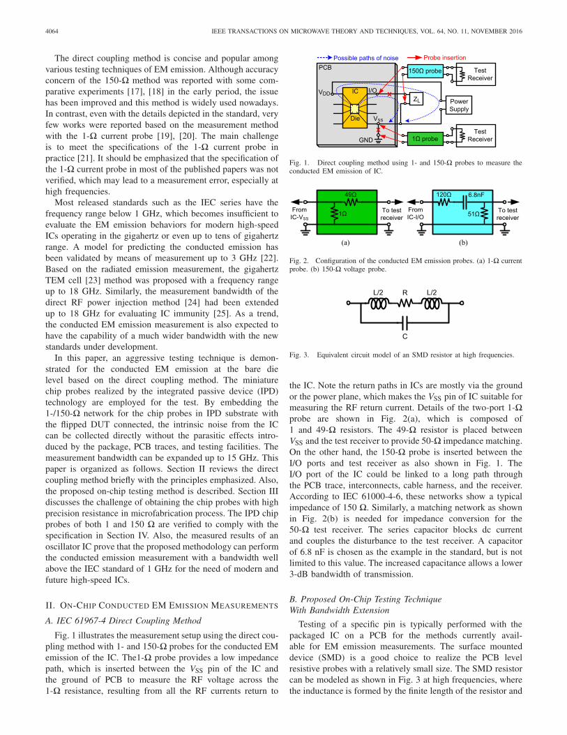
of 100 pF in the IPD design rule is employed. The resultingcorner frequency is at around 12 MHz, which is sufficientlylow, and therefore will not affect the frequency response athigh frequencies. Fig. 13 shows the measured insertion lossof the 150-� voltage probe. The result meets the specificationof 11.75 ± 2 dB with a good flatness over the measured fre-quency range. Fig. 14 shows the measured input impedance ofthe 150-� probe that also complies with the specification listedin the standard.
B. Probe Verification by IC
The experimental results verify that both probes can meetthe standard of IEC 61967-4 direct coupling method but witha much enhanced bandwidth. To further demonstrate the capa-bility of the proposed probes for the conducted EM emission
4068 IEEE TRANSACTIONS ON MICROWAVE THEORY AND TECHNIQUES, VOL. 64, NO. 11, NOVEMBER 2016
Fig. 14. Measured input impedance of the 150-� probe.
Fig. 15. Micrographs of the implemented test structures. (a) DUT (ring VCOin CMOS) and (b) flipped DUT with the 1- and 150-� probes on the IPDsubstrate.
for ICs, a ring voltage-controlled oscillator (VCO) imple-mented in the standard TSMC 1P6M 0.18-μm CMOS processis employed as the DUT, as shown in Fig. 15(a). Note that theunlabeled pads are dummy pads, which are used for additionalbonding to support the flipped IC and to ensure the connectionbetween IPD carrier and the IC. The VCO was operated undera supply voltage of 1.8 V with a power dissipation of 4.18 mW,which was then tuned to oscillate at 58 MHz for the followingexperiments. Note that the oscillator used here can emulatethe noise generators in a large-scale IC. With the largeON–OFF swings, the oscillator acts like the latent aggressor thatcould affect the normal operation of either analog or digitalcircuits. Also, the reference clock in the range of several tensof megahertz is commonly used for different applications, andthe harmonics could spread at the entire spectrum over 1 GHz.
With the test setup shown in Fig. 4, the VCO was flip-chip bonded on the IPD carrier with the 1- and 150-� probesembedded in the substrate, respectively, as shown in Fig. 15(b).The 1-� probe is connected to the VSS pin of VCO tomeasure the disturbance of EM emission, and the150-� probeis connected to the output port VOUT of the oscillator. Thematerial of the interconnection between the flipped DUT andIPD probes is gold with negligible effect on the probes at thefrequencies of interest [37]. As shown in Fig. 16(a) and (b),the measured spectra up to 3 GHz in both cases showgood agreements with the simulated results. Compared withFig. 16(b), the relatively larger discrepancy between the mea-sured and simulated results of Fig. 16(a) can be attributed to
Fig. 16. Measured spectra of (a) VSS pin of VCO using 1-� probe and(b) VOUT port of VCO using 150-� probe.
the much lower power level of the signal, which definitelyintroduces more uncertainty to the measurements. An averageuncertainty of 3-5 dB is observed during measurements forhigh-order harmonics with the power level below −60 dBm,and the worst case could be up to 8-dB variation. Also, theinaccuracy of transistor level simulation could come fromthe uncertainty of transistor compact model, since modelingof device nonlinearity (appears to be the harmonics in thespectrum) is very challenging, especially when the signal levelis low. Note that the variation of resistance of the current probecan also affect the measured spectrum, which can be verifiedby the simulation. However, using the measured S-parametersof the proposed probe for simulation shows an almost identicalspectrum compared with that using an ideal 1-� probe, whichconfirms that our probe is sufficiently accurate for widebandEM emission measurements.
It should be emphasized that the proposed method canalso work in the practical cases for specific ICs, such asan IC with several VDD-VSS pins or a complex IC madeup of building blocks with isolated power domains. Withthe customized configuration of user-defined test points, thelayout can be arranged based on the unit G-S-G probe cellon the IPD substrate to fulfill various testing requirements.Also, the layout of the unit probe cell is kept identical, andthus the measurement bandwidth will not be affected. This isvery similar with the cases for the PCB level testing, whichalso needs to have customized PCB layout for a specific ICpin configuration. Furthermore, with the rearranged pads, theproposed IPD chip probe can be used to test a packaged IC.The IC can be bonded by the solder bump on the chip probe,
CHANG et al.: WIDEBAND CONDUCTED EM EMISSION MEASUREMENTS USING IPD CHIP PROBES 4069
and the measurement bandwidth would be much better thanthe conventional probe built in the PCB level.
V. CONCLUSION
For achieving wideband measurement of conductedEM emission, we proposed a novel on-chip characterizationtechnique using IPD chip probes up to the gigahertz rangefor ICs. The size expansion technique was adopted to achievehigh precision resistance to meet the required probe specifi-cations. With the microfabrication process, the 1- and 150-�probes were demonstrated to occupy only 0.55 mm×0.77 mmand 0.83 mm × 1.49 mm, respectively. The probes wereexperimentally verified to comply with the specification ofIEC 61967-4 direct coupling method. Compared with theprobes realized by the conventional SMD with PCB, the resultsindicated that the applicable measurement frequency range canbe significantly extended up to 15 GHz. Also, a ring VCOrealized in 0.18-μm CMOS was used as the DUT for theon-chip test. The results proved that the probes can be used toperform the conducted EM emission measurement at higherfrequency bands.
[3] Integrated Circuits—Measurement of Electromagnetic Emissions, 150kHz to 1 GHz—Part 2: Measurement of Radiated Emissions—TEMCell and Wideband TEM-Cell Method, IEC 61967-2, Int. Electrotech.Commission, 2005.
[4] F. Fiori and F. Musolino, “Investigation on the effectiveness of the ICsusceptibility TEM cell method,” IEEE Trans. Electromagn. Compat.,vol. 46, no. 1, pp. 110–115, Feb. 2004.
[5] S. Deng, D. Pommerenke, T. Hubing, and D. Shin, “An experimentalinvestigation of higher order mode suppression in TEM cells,” IEEETrans. Electromagn. Compat., vol. 50, no. 2, pp. 416–419, May 2008.
[6] Integrated Circuits—Measurement of Electromagnetic Emissions, 150kHz to 1 GHz—Part 3: Measurement of Radiated Emissions—SurfaceScan Method, IEC 61967-3, Int. Electrotech. Commission, 2005.
[7] X. Dong, S. Deng, D. Beetner, and T. Hubing, “Analysis of chip-levelEMI using near-field magnetic scanning,” in Proc. IEEE Int. Symp.Electromagn. Compat., Aug. 2004, pp. 174–177.
[8] G. Langer, “Methods for precise acquisition of IC EMC characteristics,”ECE Mag., pp. 42–45, Jun. 2005.
[9] B. Minnaert, N. Stevens, and D. Pissoort, “Experimental characterizationmethods for the electromagnetic emission of inductive wireless powercircuits,” in Proc. IEEE Int. Symp. Wireless Power Transf., May 2015,pp. 1–4.
[10] C. Lochot and J.-L. Levant, “ICEM: A new standard for EMC ofIC definition and examples,” in Proc. IEEE Int. Symp. Electromagn.Compat., Aug. 2003, pp. 892–897.
[11] C. Labussiýre-Dorgan et al., “Modeling the electromagnetic emissionof a microcontroller using a single model,” IEEE Trans. Electromagn.Compat., vol. 50, no. 1, pp. 22–34, Feb. 2008.
[12] M. Ramdani, J.-L. Levant, and R. Perdriau, “ICEM model extrac-tion: A case study,” in Proc. IEEE Int. Symp. Electromagn. Compat.,Aug. 2004, pp. 969–973.
[13] K. H. Kim and J. E. Schutt-Ainé, “Analysis and modeling of hybridplanar-type electromagnetic-bandgap structures and feasibility study onpower distribution network applications,” IEEE Trans. Microw. TheoryTechn., vol. 56, no. 1, pp. 178–186, Jan. 2008.
[14] T.-K. Wang, T.-W. Han, and T.-L. Wu, “A novel power/ground layerusing artificial substrate EBG for simultaneously switching noisesuppression,” IEEE Trans. Microw. Theory Techn., vol. 56, no. 5,pp. 1164–1171, May 2008.
[15] T.-K. Wang, C.-Y. Hsieh, H.-H. Chuang, and T.-L. Wu, “Design andmodeling of a stopband-enhanced EBG structure using ground surfaceperturbation lattice for power/ground noise suppression,” IEEE Trans.Microw. Theory Techn., vol. 57, no. 8, pp. 2047–2054, Aug. 2009.
[16] Integrated Circuits—-Measurement of Electromagnetic Emissions, 150kHz to 1 GHz—Part 4: Measurement of Conducted Emissions—1/150Direct Coupling Method, IEC 61967-4, Int. Electrotech. Commission,2006.
[17] F. Fiori and S. Pignari, “Analysis of a test setup for the characterizationof integrated circuits electromagnetic emissions,” in Proc. IEEE Int.Symp. Electromagn. Compat., Aug. 2000, pp. 375–378.
[18] B. Deutschmann, G. Winkler, and R. Jungreithmair, “Measuring theelectromagnetic emissions of integrated circuits with IEC 61967-4 (themeasuring method and its weaknesses),” in Proc. IEEE Int. Symp.Electromagn. Compat., Aug. 2002, pp. 407–412.
[19] F. Fiori and F. Musolino, “Comparison of IC conducted emissionmeasurement methods,” IEEE Trans. Instrum. Meas., vol. 52, no. 3,pp. 839–845, Jun. 2003.
[20] I. S. Stievano et al., “Behavioral modeling of IC memories frommeasured data,” IEEE Trans. Instrum. Meas., vol. 60, no. 10,pp. 3471–3479, Oct. 2011.
[21] Y.-C. Chang et al., “Investigation on realizing 1 � current probecomplied with IEC 61967-4 direct coupling method,” in Proc. Int. Symp.Electromagn. Compat., May 2014, pp. 573–576.
[22] N. Berbel, R. Fernandez-Garcia, and I. Gil, “Characterization andmodeling of the conducted emission of integrated circuits up to 3 GHz,”IEEE Trans. Electromagn. Compat., vol. 56, no. 4, pp. 878–884,Aug. 2014.
[23] D. Konigstein and D. Hansen, “A new family of TEM-cells with enlargedbandwidth and optimized working volume,” in Proc. 7th Int. ZurichSymp. Tech. Exhibit. Electromagn. Compat., Mar. 1987, pp. 127–132.
[24] Integrated Circuits—Measurement of Electromagnetic Immunity, 150kHz to 1 GHz—Part 4: Direct RF Power Injection Method, IEC 62132-4,Int. Electrotech. Commission, 2006.
[25] Y.-C. Chang, S. S. H. Hsu, Y.-T. Chang, C.-K. Chen, H.-C. Cheng, andD.-C. Chang, “The direct RF power injection method up to 18 GHz forinvestigating IC’s susceptibility,” in Proc. Int. Workshop Electromagn.Compat. Integr. Circuits (EMC Compo), Dec. 2013, pp. 167–170.
[26] C.-Y. Hsiao, S. S. H. Hsu, and D.-C. Chang, “A compact V-bandbandpass filter in IPD technology,” IEEE Microw. Wireless Compon.Lett., vol. 21, no. 10, pp. 531–533, Oct. 2011.
[27] C.-Y. Hsiao, Y.-C. Huang, and T.-L. Wu, “An ultra-compact common-mode bandstop filter with modified-T circuits in integrated passivedevice (IPD) process,” IEEE Trans. Microw. Theory Techn., vol. 63,no. 11, pp. 3624–3631, Nov. 2015.
[28] C.-Y. Hsiao, C.-H. Cheng, and T.-L. Wu, “A new broadbandcommon-mode noise absorption circuit for high-speed differential dig-ital systems,” IEEE Trans. Microw. Theory Techn., vol. 63, no. 6,pp. 1894–1901, Jun. 2015.
[29] S. Shim and S. Hong, “A CMOS power amplifier with integrated-passive-device spiral-shaped directional coupler for mobile UHFRFID reader,” IEEE Trans. Microw. Theory Techn., vol. 59, no. 11,pp. 2888–2897, Nov. 2011.
[30] Y.-S. Lin and J.-H. Lee, “Miniature Butler matrix design using glass-based thin-film integrated passive device technology for 2.5-GHzapplications,” IEEE Trans. Microw. Theory Techn., vol. 61, no. 7,pp. 2594–2602, Jul. 2013.
[31] L.-C. Hsu, Y.-L. Wu, J.-Y. Zou, H. N. Chu, and T.-G. Ma, “Periodicsynthesized transmission lines with 2-D routing capability and itsapplications to power divider and couplers using integrated passivedevice process,” IEEE Trans. Microw. Theory Techn., vol. 64, no. 2,pp. 493–501, Feb. 2016.
[32] H.-S. Yang, J.-H. Chen, and Y.-J. E. Chen, “A wideband and highlysymmetric multi-port parallel combining transformer technology,” IEEETrans. Microw. Theory Techn., vol. 63, no. 11, pp. 3671–3680,Nov. 2015.
[33] H. Lee, C. Park, and S. Hong, “A quasi-four-pair class-E CMOSRF power amplifier with an integrated passive device transformer,”IEEE Trans. Microw. Theory Techn., vol. 57, no. 4, pp. 752–759,Apr. 2009.
[34] S. Wang and W.-J. Lin, “A 10/24-GHz CMOS/IPD monopulse receiverfor angle-discrimination radars,” IEEE Trans. Circuits Syst. I, Reg.Papers, vol. 61, no. 10, pp. 2999–3006, Oct. 2014.
[35] A. Hastings, The Art of Analog Layout, 2nd ed. Englewood Cliffs, NJ,USA: Prentice-Hall, 2005.
4070 IEEE TRANSACTIONS ON MICROWAVE THEORY AND TECHNIQUES, VOL. 64, NO. 11, NOVEMBER 2016
[36] Y.-C. Chang, P.-Y. Wang, S. S. H. Hsu, Y.-T. Chang, C.-K. Chen, andD.-C. Chang, “Impact and improvement of resistor process variationon RF passive circuit design in integrated passive devices (IPD) tech-nology,” in Proc. Int. Conf. Solid State Devices Mater., Sep. 2015,pp. 74–75.
[37] Y.-C. Chang, D.-C. Chang, S. S. H. Hsu, J.-H. Lee, S.-G. Lin, andY.-Z. Juang, “A matrix-computation based methodology for extractingthe S-parameters of interconnects in advanced packaging technologies,”in Proc. IEEE Asia–Pacific Microw. Conf., Dec. 2011, pp. 1909–1912.
Yin-Cheng Chang received the B.S. degree inelectronics engineering and the M.S. degree in com-munication engineering from Feng Chia University,Taichung, Taiwan, in 2003 and 2005, respectively.He is currently pursuing the Ph.D. degree in elec-tronics engineering at National Tsing Hua Univer-sity, Hsinchu, Taiwan.
From 2005 to 2009, he was an Assistant ResearchFellow with the National Chip Implementation Cen-ter, Hsinchu, where he was responsible for high fre-quency measurement technology development and
system-in-package (SiP) design. Since 2010, he has been an AssociateResearch Fellow. His current research interests include RF/MW circuit designand measurement, SiP application, signal integrity, power integrity, andelectromagnetic compatibility.
Mr. Chang is a member of the Phi-Tau-Phi honorary Scholar Society.
Ping-Yi Wang was born in Kinmen, Taiwan,in 1984. He received the B.S. degree in electronicengineering from Chung Yuan Christian University,Taoyuan, Taiwan, in 2007, and the M.S. degreein electronic engineering from National Tsing HuaUniversity, Hsinchu, Taiwan, in 2009, where he iscurrently pursuing the Ph.D. degree in electronicsengineering.
His current research interests include frequencysynthesizers, low power RF front-end circuits, andmixed-signal circuits.
Da-Chiang Chang was born in Taipei, Taiwan,in 1966. He received the B.S. and M.S. degreesin electrical engineering from National Tsing-HuaUniversity, Hsinchu, Taiwan, in 1989 and 1991,respectively, and the Ph.D. degree in electronicengineering from the National Taiwan University ofScience and Technology, Taipei, in 2001.
From 1991 to 1993, he was an Officer at theRepublic of China Air Force, Kaohsiung, Taiwan.In 1993, he joined as an Instructor with the Depart-ment of Electronic Engineering, Chinese Institute
of Technology, Taipei, and became an Associate Professor in 2001. From2002 to 2003, he was with the United Microelectronics Cooperation, Hsinchu.From 2003 to 2005, he was with the Acer Laboratories Inc., Taipei. In2005, he joined the National Chip Implementation Center, Hsinchu, wherehe is currently a Research Fellow and the Division Director in charge of thechip implementation services, and the development of RF system-in-package,millimeter wave circuit, high-speed data link, and the signal integrity designenvironment and measurement technologies.
Shawn S. H. Hsu (M’04) was born in Tainan,Taiwan. He received the B.S. degree from NationalTsing Hua University, Hsinchu, Taiwan, in 1992, andthe M.S. and Ph.D. degrees from the University ofMichigan, Ann Arbor, MI, USA, in 1997 and 2003,respectively.
In 2014, he was a Distinguished Professor withNational Tsing Hua University. He is currentlya Professor with the Department of ElectricalEngineering, Institute of Electronics Engineering,National Tsing Hua University. He is involved in
the design, fabrication, and the modeling of high-frequency transistors andinterconnects. His current research interests include the design of monolithicmicrowave integrated circuits and RF integrated circuits using Si/III-V-basedtechnologies, heterogeneous integration using system-in-package, and 3-Dintegrated circuit technology for high-speed wireless/optical communications.