IEEE TRANSACTIONS ON NUCLEAR SCIENCE, VOL. 54, NO. 4, AUGUST 2007 843
A Prototype Three-Dimensional Position SensitiveCdZnTe Detector Array
Feng Zhang, Zhong He, Senior Member, IEEE, and Carolyn E. Seifert, Member, IEEE
Abstract—A new CdZnTe gamma-ray spectrometer system thatemploys two layers of modular detector arrays is being developedunder the collaboration between the University of Michigan andthe Pacific Northwest National Labaratory (PNNL). Each layercan accommodate up to three by three 3-dimensional positionsensitive CdZnTe gamma-ray spectrometers. This array system isbased on the newly developed VAS_UM/TAT4 ASIC readout elec-tronics. Each of the nine detector modules consists of a pixellatedCdZnTe detector and a VAS_UM/TAT4 ASIC front-end board.Each 1.5 1.5 1.0 cm3 CdZnTe detector employs an arrayof 11 by 11 pixellated anodes and a planar cathode. The energydepositions and 3-dimensional positions of individual interactionsof each incident gamma ray can be obtained from pulse ampli-tude, location of each pixel anode and the drift time of electrons.Ten detectors were tested individually and half of them achievedresolution of 1 0% FWHM at 662 keV for single-pixel events( 30% of all 662 keV full energy deposition events). Two of themwere tested in a simple array to verify that the upgrade to an arraysystem does not sacrifice the performance of individual detectors.Experimental results of individual detectors and a two-detectorarray system are presented, and possible causes for several worseperforming detectors are discussed.
Index Terms—CdZnTe, detector array, gamma-ray spectrom-eter, position sensitive, three-dimensional (3-D).
I. INTRODUCTION
TRULY HAND-HELD gamma-ray detectors with excellentenergy resolution ( FWHM at 662 keV), high
efficiency and imaging capability are urgently needed forhomeland security and nuclear non-proliferation applications.Mechanically cooled HPGe detectors are commercially avail-able but are still too bulky to be called a “hand-held” device [1].To date, the most promising candidates are still wide band-gapsemiconductors, such as CdZnTe and . In the past tenyears, several single-polarity charge-sensing techniques, suchas coplanar-grid [2], Frisch-grid [3]–[5], or simple pixellatedanodes [6], [7], have been developed successfully to mitigatethe hole trapping problem and to improve energy resolution onlarger volume CdZnTe and detectors. However, materialnon-uniformity and electron trapping problems in these mate-rials still limit the energy resolution of large volume (with an
Manuscript received January 15, 2007; revised May 21, 2007. This work wassupported by the Department of Energy (DOE) NA-22 Office through the Pa-cific Northwest National Laboratory (PNNL), and the Department of Defense,Defense Threat Reduction Agency (DoD, DTRA).
F. Zhang and Z. He are with the Department of Nuclear Engineering and Radi-ological Sciences, University of Michigan, Ann Arbor, MI 48109 USA (e-mail:[email protected]).
C. E. Seifert is with the Pacific Northwest National Laboratory, Richland, WA99352 USA (e-mail: [email protected]).
Digital Object Identifier 10.1109/TNS.2007.902354
area about 2 and a thickness about 1 cm) CdZnTe detectorsto be worse than 2% FWHM at 662 keV.
Our approach to overcome the non-uniform detector responseis the three-dimensional (3-D) position-sensing technique [8].We read out signals from both the pixellated anodes and thecathode from which we can derive the deposited energy and 3-Dcoordinates of each individual gamma-ray interaction. Havingthe 3-D coordinates of each interaction, a correction for mate-rial non-uniformity and electron trapping in 3-dimensions be-comes feasible. The first two generations of 3-D position-sen-sitive CdZnTe spectrometers were developed and reported in1998 [9] and 2003 [10]. In 2004, we reported two 3-D posi-tion sensitive CdZnTe spectrometers coupled with the 3rd gen-eration VAS3.1/TAT3 ASIC readout systems [11]. The CdZnTedetectors used in these two systems were 1.5 1.5 1.0single crystals employing 11 by 11 pixellated anodes. Both sys-tems achieved better than 1% FWHM resolution at 662 keV forsingle-pixel events and one system was even better than 0.8%FWHM. Other researchers are also exploring similar position-sensitive correction techniques [12], [13] for single-pixel events.The unique advantage of our device is its ability to fully recon-struct multiple gamma-ray interaction events (energies and 3-Dcoordinates) by measuring the electron drift times, which makesit possible to perform intelligent gamma-ray spectroscopy [14]and Compton imaging [15]. However, low efficiency due to thesmall sensitive volume (2.25 ) limited their usage to labo-ratory demonstrations.
We are now developing the first truly hand-held 3-D posi-tion sensitive CdZnTe detector array. The upgrade in the ASICand readout electronics from a single detector system to an ex-pandable array system was done by Gamma-Medica-Ideas Inc.and was reported last year [16]. The most significant improve-ment from the previous single detector system is that the ASICchip and the front-end board are miniaturized to closely matchthe size of the detector, thus multiple detector modules can beplugged on the motherboard to form an expandable detectorarray.
The goal of this project is to build a system in which multiple3-D CdZnTe detector modules can be tiled together to achievedetection volume greater than 40 . This configuration al-lows the expansion of detector area to achieve higher detec-tion efficiency while maintaining the excellent energy resolu-tion ( FWHM at 662 keV for single-pixel events).
II. SYSTEM DESCRIPTION
A. Detector Module
The fundamental element of the array system is the detectormodule, which consists of an ASIC front-end board and a
844 IEEE TRANSACTIONS ON NUCLEAR SCIENCE, VOL. 54, NO. 4, AUGUST 2007
TABLE IAVERAGE AND PIXEL MAP OF ENERGY RESOLUTION AND ELECTRON MOBILITY-LIFETIME PRODUCTS FOR TEN INDIVIDUAL DETECTORS
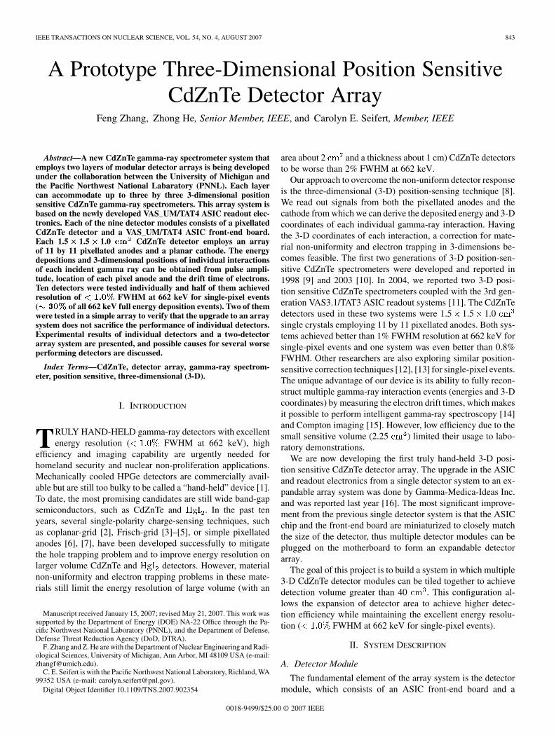
Fig. 1. Photos of the CdZnTe detector, the VAS_UM/TAT4 ASIC front-endboards and the detector array with four detector modules installed. (A)1.5� 1.5� 1.0 cm CdZnTe crystal bonded on a ceramic substrate withthree 42-pin 0.8 mm pitch pin connectors (from eV-PRODUCTS). (B) ASICfront-end board, three 42-pin 0.8 mm pitch socket connectors are used on theside facing the detector substrate, one 40-pin 1.0 mm pitch connector is onthe side facing the motherboard, the 129 channel VAS_UM/TAT4 ASIC isenclosed inside the heat-sink. The area of each frond-end board is 2.2 by 2.2cm . (C) Four detector modules are installed on the motherboard.
1.5 1.5 1.0 pixellated CdZnTe detector. The integra-tion of 129 channels of energy-timing circuitries into one ASICchip, which we named VAS_UM/TAT4, has made it possible toreduce the dimensions of the front-end board from about 4 by 6inches in the old single detector system to 2.2 2.2 in thenew array system. Fine pitch connectors are used to couple theCdZnTe detector with the front-end board to form the detectormodule, and to connect the detector module to the motherboard.Pictures from the actual detector modules can be seen in Fig. 1.
B. Array Readout System
The array readout system mainly consists of a motherboardand a digital readout board. A FPGA on the motherboard con-trols all the ASICs. One digital readout board can synchronizesignals read out from up to four motherboards for multi-layer
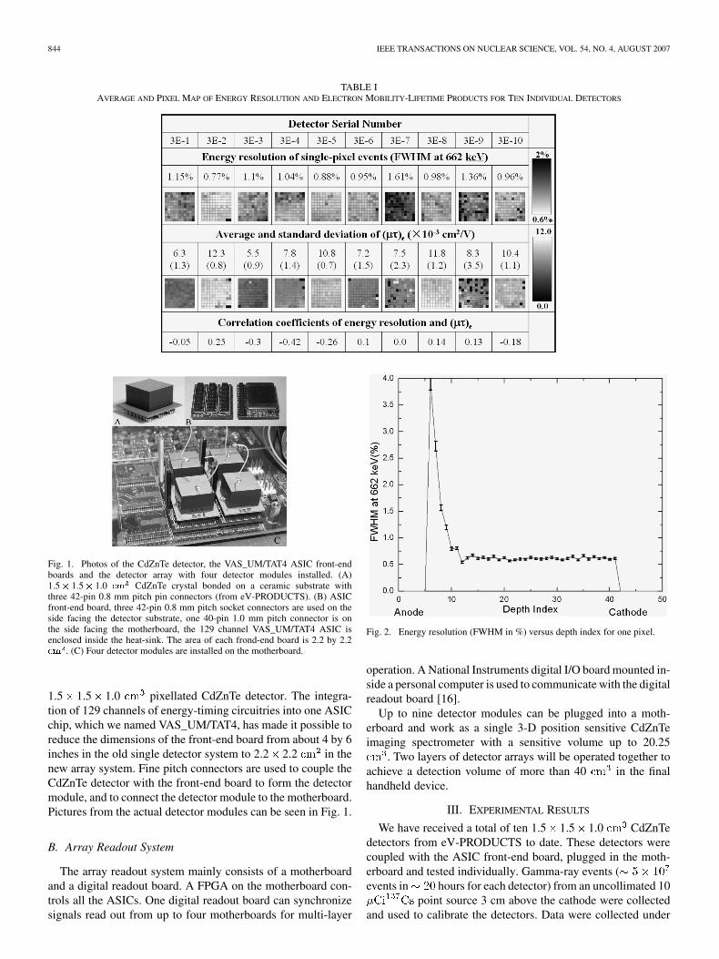
Fig. 2. Energy resolution (FWHM in %) versus depth index for one pixel.
operation. A National Instruments digital I/O board mounted in-side a personal computer is used to communicate with the digitalreadout board [16].
Up to nine detector modules can be plugged into a moth-erboard and work as a single 3-D position sensitive CdZnTeimaging spectrometer with a sensitive volume up to 20.25
. Two layers of detector arrays will be operated together toachieve a detection volume of more than 40 in the finalhandheld device.
III. EXPERIMENTAL RESULTS
We have received a total of ten 1.5 1.5 1.0 CdZnTedetectors from eV-PRODUCTS to date. These detectors werecoupled with the ASIC front-end board, plugged in the moth-erboard and tested individually. Gamma-ray events (events in hours for each detector) from an uncollimated 10
point source 3 cm above the cathode were collectedand used to calibrate the detectors. Data were collected under
ZHANG et al.: A PROTOTYPE THREE-DIMENSIONAL POSITION SENSITIVE CDZNTE DETECTOR ARRAY 845
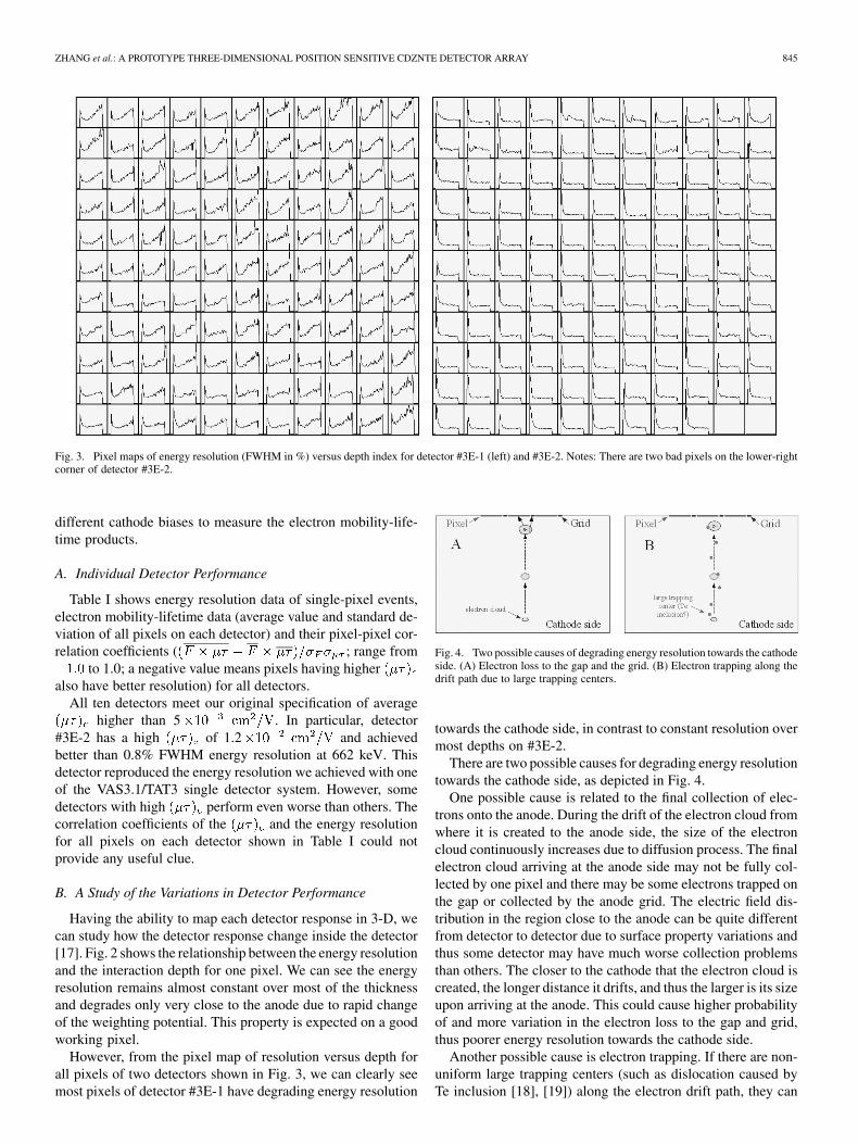
Fig. 3. Pixel maps of energy resolution (FWHM in %) versus depth index for detector #3E-1 (left) and #3E-2. Notes: There are two bad pixels on the lower-rightcorner of detector #3E-2.
different cathode biases to measure the electron mobility-life-time products.
A. Individual Detector Performance
Table I shows energy resolution data of single-pixel events,electron mobility-lifetime data (average value and standard de-viation of all pixels on each detector) and their pixel-pixel cor-relation coefficients ( ; range from
to 1.0; a negative value means pixels having higheralso have better resolution) for all detectors.
All ten detectors meet our original specification of averagehigher than 5 . In particular, detector
#3E-2 has a high of 1.2 and achievedbetter than 0.8% FWHM energy resolution at 662 keV. Thisdetector reproduced the energy resolution we achieved with oneof the VAS3.1/TAT3 single detector system. However, somedetectors with high perform even worse than others. Thecorrelation coefficients of the and the energy resolutionfor all pixels on each detector shown in Table I could notprovide any useful clue.
B. A Study of the Variations in Detector Performance
Having the ability to map each detector response in 3-D, wecan study how the detector response change inside the detector[17]. Fig. 2 shows the relationship between the energy resolutionand the interaction depth for one pixel. We can see the energyresolution remains almost constant over most of the thicknessand degrades only very close to the anode due to rapid changeof the weighting potential. This property is expected on a goodworking pixel.
However, from the pixel map of resolution versus depth forall pixels of two detectors shown in Fig. 3, we can clearly seemost pixels of detector #3E-1 have degrading energy resolution
Fig. 4. Two possible causes of degrading energy resolution towards the cathodeside. (A) Electron loss to the gap and the grid. (B) Electron trapping along thedrift path due to large trapping centers.
towards the cathode side, in contrast to constant resolution overmost depths on #3E-2.
There are two possible causes for degrading energy resolutiontowards the cathode side, as depicted in Fig. 4.
One possible cause is related to the final collection of elec-trons onto the anode. During the drift of the electron cloud fromwhere it is created to the anode side, the size of the electroncloud continuously increases due to diffusion process. The finalelectron cloud arriving at the anode side may not be fully col-lected by one pixel and there may be some electrons trapped onthe gap or collected by the anode grid. The electric field dis-tribution in the region close to the anode can be quite differentfrom detector to detector due to surface property variations andthus some detector may have much worse collection problemsthan others. The closer to the cathode that the electron cloud iscreated, the longer distance it drifts, and thus the larger is its sizeupon arriving at the anode. This could cause higher probabilityof and more variation in the electron loss to the gap and grid,thus poorer energy resolution towards the cathode side.
Another possible cause is electron trapping. If there are non-uniform large trapping centers (such as dislocation caused byTe inclusion [18], [19]) along the electron drift path, they can
846 IEEE TRANSACTIONS ON NUCLEAR SCIENCE, VOL. 54, NO. 4, AUGUST 2007
Fig. 5. (A) Depth separated spectra for a pixel. (B) Depth separated spectra for the cathode signal. (C) Photopeak region of depth separated cathode spectra. (D)Photopeak region of depth separated cathode spectra for all pixels aligned to the same centroid position.
cause larger fluctuation in electron trapping if electrons passmore trapping sites. It is evident that the longer the drift length,the larger the variation in electron loss due to trapping. As dis-cussed in [17], 3-D position sensing and correction cannot im-prove such variations that are in a scale smaller than the pixelpitch.
It is impossible to tell from the anode signal which one of theabove two caused the degrading resolution towards the cathodeside, because the anode signal does not contain any informationwhere the electrons are lost.
But the cathode signal is only affected by the second casesince electrons trapped on the anode surface does not affect thecathode signal. Therefore a study in the cathode signal may re-veal which cause degrades energy resolution.
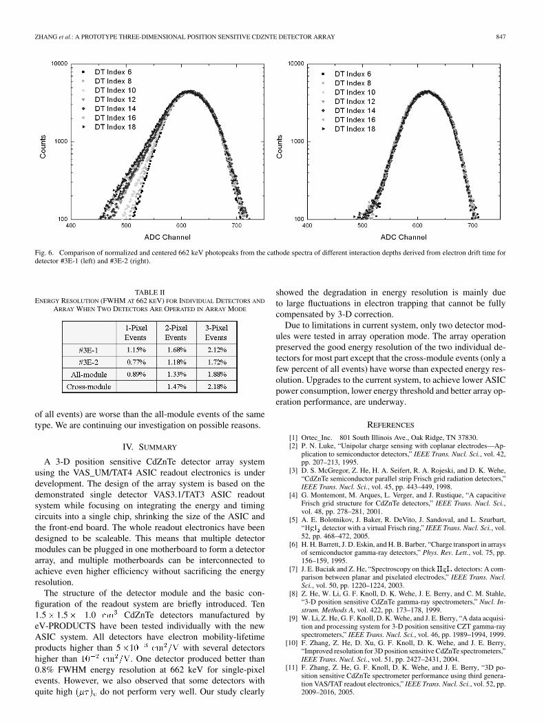
For comparison, Fig. 5(a) shows depth separated spectra ofa source for a pixel, while Fig. 5(b) shows depth sep-arated cathode spectra for this same pixel. We can clearly seethat the 662 keV photopeak position in the cathode spectra hasa linear relationship with the interaction depth due to the linearweighting potential of the cathode. For each depth, we focusonly on the photopeak region (cf. Fig. 5(c). First, align the pho-topeaks at the same depth for all anode pixels to the same cen-troid position (to increase counts in the peak and reduce statis-tical fluctuation), and then align all the photopeaks to the samecentroid position [cf. Fig. 5(d)] to compare their shape from alldepths.
Fig. 6 shows the aligned and normalized cathode spectra(photopeak region) for different depths. We can clearly see thatthe good detector (#3E-2) has consistent peak shape throughoutall depths, while the worse detector (#3E-1) has increasing lowenergy tails towards the cathode side indicating the increased
electron trapping. These results clearly reveal that the degradingenergy resolution is due to fluctuations in electron trapping.
C. Array Performance
Due to higher-than-expected ASIC power consumptioncaused by a design flaw in the ASIC, the system runs hotwith more than two detector modules plugged in. To be safe,we only tested two detectors (#3E-1 and #3E-2) in the arrayoperation mode. The energy resolutions for individual detectormodules and two modules as an array are listed in Table II. The“all-module” events mean the gamma rays interact in either oneof the detector or both, while the “cross-module” events arethose events in which gamma rays interact and deposit energiesin both detectors.
For each individual detector in the two-detector array system,the energy resolutions are almost the same as when they wereoperated individually (only one detector plugged in the moth-erboard) and also similar to the results with the one-detectorVAS3.1/TAT3 system [11]. This response shows that the mi-gration from one-detector system to a multiple-detector arraysystem is successful. As discussed in [11], the energy resolutiondegradation with increasing number of interactions is partly dueto added electronic noise from multiple pixels and worse depthresolution from timing, but these factors cannot fully accountfor the degradation. Undetectable (below threshold) charge lossto the grid, the gap or neighboring pixels is a direction we areinvestigating.
For the array performance, we can see that the resolutionsof all-module events are between the resolutions of each indi-vidual detector for the same type of events, as expected. How-ever, the resolutions of the cross-module events (a few percent
ZHANG et al.: A PROTOTYPE THREE-DIMENSIONAL POSITION SENSITIVE CDZNTE DETECTOR ARRAY 847
Fig. 6. Comparison of normalized and centered 662 keV photopeaks from the cathode spectra of different interaction depths derived from electron drift time fordetector #3E-1 (left) and #3E-2 (right).
TABLE IIENERGY RESOLUTION (FWHM AT 662 KEV) FOR INDIVIDUAL DETECTORS AND
ARRAY WHEN TWO DETECTORS ARE OPERATED IN ARRAY MODE
of all events) are worse than the all-module events of the sametype. We are continuing our investigation on possible reasons.
IV. SUMMARY
A 3-D position sensitive CdZnTe detector array systemusing the VAS_UM/TAT4 ASIC readout electronics is underdevelopment. The design of the array system is based on thedemonstrated single detector VAS3.1/TAT3 ASIC readoutsystem while focusing on integrating the energy and timingcircuits into a single chip, shrinking the size of the ASIC andthe front-end board. The whole readout electronics have beendesigned to be scaleable. This means that multiple detectormodules can be plugged in one motherboard to form a detectorarray, and multiple motherboards can be interconnected toachieve even higher efficiency without sacrificing the energyresolution.
The structure of the detector module and the basic con-figuration of the readout system are briefly introduced. Ten1.5 1.5 1.0 CdZnTe detectors manufactured byeV-PRODUCTS have been tested individually with the newASIC system. All detectors have electron mobility-lifetimeproducts higher than 5 with several detectorshigher than . One detector produced better than0.8% FWHM energy resolution at 662 keV for single-pixelevents. However, we also observed that some detectors withquite high do not perform very well. Our study clearly
showed the degradation in energy resolution is mainly dueto large fluctuations in electron trapping that cannot be fullycompensated by 3-D correction.
Due to limitations in current system, only two detector mod-ules were tested in array operation mode. The array operationpreserved the good energy resolution of the two individual de-tectors for most part except that the cross-module events (only afew percent of all events) have worse than expected energy res-olution. Upgrades to the current system, to achieve lower ASICpower consumption, lower energy threshold and better array op-eration performance, are underway.
REFERENCES
[1] Ortec_Inc. 801 South Illinois Ave., Oak Ridge, TN 37830.[2] P. N. Luke, “Unipolar charge sensing with coplanar electrodes—Ap-
[3] D. S. McGregor, Z. He, H. A. Seifert, R. A. Rojeski, and D. K. Wehe,“CdZnTe semiconductor parallel strip Frisch grid radiation detectors,”IEEE Trans. Nucl. Sci., vol. 45, pp. 443–449, 1998.
[4] G. Montemont, M. Arques, L. Verger, and J. Rustique, “A capacitiveFrisch grid structure for CdZnTe detectors,” IEEE Trans. Nucl. Sci.,vol. 48, pp. 278–281, 2001.
[5] A. E. Bolotnikov, J. Baker, R. DeVito, J. Sandoval, and L. Szurbart,“HgI detector with a virtual Frisch ring,” IEEE Trans. Nucl. Sci., vol.52, pp. 468–472, 2005.
[6] H. H. Barrett, J. D. Eskin, and H. B. Barber, “Charge transport in arraysof semiconductor gamma-ray detectors,” Phys. Rev. Lett., vol. 75, pp.156–159, 1995.
[7] J. E. Baciak and Z. He, “Spectroscopy on thickHgI detectors: A com-parison between planar and pixelated electrodes,” IEEE Trans. Nucl.Sci., vol. 50, pp. 1220–1224, 2003.
[8] Z. He, W. Li, G. F. Knoll, D. K. Wehe, J. E. Berry, and C. M. Stahle,“3-D position sensitive CdZnTe gamma-ray spectrometers,” Nucl. In-strum. Methods A, vol. 422, pp. 173–178, 1999.
[9] W. Li, Z. He, G. F. Knoll, D. K. Wehe, and J. E. Berry, “A data acquisi-tion and processing system for 3-D position sensitive CZT gamma-rayspectrometers,” IEEE Trans. Nucl. Sci., vol. 46, pp. 1989–1994, 1999.
[10] F. Zhang, Z. He, D. Xu, G. F. Knoll, D. K. Wehe, and J. E. Berry,“Improved resolution for 3D position sensitive CdZnTe spectrometers,”IEEE Trans. Nucl. Sci., vol. 51, pp. 2427–2431, 2004.
[11] F. Zhang, Z. He, G. F. Knoll, D. K. Wehe, and J. E. Berry, “3D po-sition sensitive CdZnTe spectrometer performance using third genera-tion VAS/TAT readout electronics,” IEEE Trans. Nucl. Sci., vol. 52, pp.2009–2016, 2005.
848 IEEE TRANSACTIONS ON NUCLEAR SCIENCE, VOL. 54, NO. 4, AUGUST 2007
[12] J. L. Matteson, R. T. Skelton, M. R. Pelling, S. Suchy, V. B. Cajipe, M.Clajus, S. Hayakawa, and T. O. Tumer, “CZT detectors read out withthe RENA-2 ASIC,” presented at the IEEE Nuclear Science Symp.,Puerto Rico, Oct. 23-29, 2005.
[13] A. Shor, Y. Eisen, and I. Mardor, “Spectroscopy for Compton interac-tion in pixelated CdZnTe detectors,” IEEE Trans. Nucl. Sci., vol. 53,pp. 1656–1658, 2006.
[14] C. E. Lehner, Z. He, and G. F. Knoll, “Intelligent gamma-ray spec-troscopy using 3-D position-sensitive detectors,” IEEE Trans. Nucl.Sci., vol. 50, pp. 1090–1097, 2003.
[15] C. E. Lehner, Z. He, and F. Zhang, “4� compton imaging using a 3-Dposition-sensitive CdZnTe detector via weighted list-mode maximumlikelihood,” IEEE Trans. Nucl. Sci., vol. 51, pp. 1618–1624, 2004.
[16] F. Zhang and Z. He, “New readout electronics for 3-D position sensi-tive CdZnTe/HgI2 detector arrays,” IEEE Trans. Nucl. Sci., vol. 53, pp.3021–3027, 2006.
[17] F. Zhang, Z. He, and D. Xu, “Analysis of detector response using 3-Dposition sensitive CZT gamma-ray spectrometers,” IEEE Trans. Nucl.Sci., vol. 51, pp. 3295–3299, 2004.
[18] S. A. Soldner, A. J. Narvett, D. E. Covalt, and C. Szeles, “Charac-terization of the charge transport uniformity of CdZnTe crystals forlarge-volume nuclear detector applications,” IEEE Trans. Nucl. Sci.,vol. 51, pp. 2443–2447, 2004.
[19] M. Amman, J. S. Lee, and P. N. Luke, “Electron trapping nonunifor-mity in high-pressure-Bridgeman-grown CdZnTe,” J. Appl. Phys., vol.92, pp. 3198–3206, 2002.