SANDIA REPORT SAND2012-7548 Unlimited Release Printed September 2012 III-nitride core-shell nanowire arrayed solar cells Jonathan J. Wierer, Jr., Qiming Li, Daniel D. Koleske, Stephen R. Lee, and George T. Wang Prepared by Sandia National Laboratories Albuquerque, New Mexico 87185 and Livermore, California 94550 Sandia National Laboratories is a multi-program laboratory managed and operated by Sandia Corporation, a wholly owned subsidiary of Lockheed Martin Corporation, for the U.S. Department of Energy's National Nuclear Security Administration under contract DE-AC04-94AL85000. Approved for public release; further dissemination unlimited.
Transcript
SANDIA REPORT SAND2012-7548 Unlimited Release Printed September 2012
III-nitride core-shell nanowire arrayed solar cells Jonathan J. Wierer, Jr., Qiming Li, Daniel D. Koleske, Stephen R. Lee, and George T. Wang Prepared by Sandia National Laboratories Albuquerque, New Mexico 87185 and Livermore, California 94550 Sandia National Laboratories is a multi-program laboratory managed and operated by Sandia Corporation, a wholly owned subsidiary of Lockheed Martin Corporation, for the U.S. Department of Energy's National Nuclear Security Administration under contract DE-AC04-94AL85000. Approved for public release; further dissemination unlimited.
2
Issued by Sandia National Laboratories, operated for the United States Department of Energy by Sandia Corporation. NOTICE: This report was prepared as an account of work sponsored by an agency of the United States Government. Neither the United States Government, nor any agency thereof, nor any of their employees, nor any of their contractors, subcontractors, or their employees, make any warranty, express or implied, or assume any legal liability or responsibility for the accuracy, completeness, or usefulness of any information, apparatus, product, or process disclosed, or represent that its use would not infringe privately owned rights. Reference herein to any specific commercial product, process, or service by trade name, trademark, manufacturer, or otherwise, does not necessarily constitute or imply its endorsement, recommendation, or favoring by the United States Government, any agency thereof, or any of their contractors or subcontractors. The views and opinions expressed herein do not necessarily state or reflect those of the United States Government, any agency thereof, or any of their contractors. Printed in the United States of America. This report has been reproduced directly from the best available copy. Available to DOE and DOE contractors from U.S. Department of Energy Office of Scientific and Technical Information P.O. Box 62 Oak Ridge, TN 37831 Telephone: (865) 576-8401 Facsimile: (865) 576-5728 E-Mail: [email protected] Online ordering: http://www.osti.gov/bridge Available to the public from U.S. Department of Commerce National Technical Information Service 5285 Port Royal Rd. Springfield, VA 22161 Telephone: (800) 553-6847 Facsimile: (703) 605-6900 E-Mail: [email protected] Online order: http://www.ntis.gov/help/ordermethods.asp?loc=7-4-0#online
III-nitride core-shell nanowire arrayed solar cells
Jonathan J. Wierer, Jr,* Qiming Li**, Daniel D. Koleske**, Stephen R. Lee*, and George T. Wang**
*Semiconductor and Material and Device Sciences **Advanced Material Sciences
Sandia National Laboratories
P.O. Box 5800 Albuquerque, New Mexico 87185-MS1086
Abstract
A solar cell based on a III-nitride hybrid nanowire-film architecture is demonstrated. It consists of a vertically-aligned array of InGaN/GaN multi-quantum well core-shell nanowires, electrically connected by a coalesced p-type InGaN canopy layer. This hybrid structure allows for standard planar device processing, solving an important challenge with nanowire device integration. It also enables various advantages such as higher indium composition InGaN layers via elastic strain relief, efficient carrier collection through thin layers, and enhanced light trapping. This proof-of-concept nanowire-based device presents a path forward for high-efficiency III-nitride solar cells. Fabricated III-nitride nanowire solar cells exhibit a photoresponse out to 2.1eV and short circuit current density of ~1 mA/cm2 (1 sun AM1.5G).
Distribution [can go on an even or an odd page] .......................................................................... 20
FIGURES Figure 1. Schematic illustrating (a) the steps to form the hybrid nanowire film solar cell, and (b) a cross-section of the final structure……………………………………………………………… 9 Figure 2. Scanning electron microscope images showing (a) the nanowire template, (b) the nanowires after MQW growth, (c) the structure after p-InGaN canopy growth, and (d) the canopy layer from the top……………………………………………………………………………….. 10 Figure 3. STEM images of (a) a row of nanowires, (b) a single nanowire illustrating the MQW, and p-type GaN layers, and (c) a close up of the MQWs on different facets…………………… 11 Figure 4. A (a) top view of a simple solar cell, and (a) a schematic cross-section of the completed device……………………………………………………………………………………………. 12 Figure 5. EQE of the III-nitride nanowire solar cell. Inset is a close-up at lower energies…….. 13 Figure 6. JV characteristic under dark and 1 sun conditions……………………………………. 14
6
NOMENCLATURE Å angstromsm micrometer A amps Al aluminum AM1.5G average solar spectrum on earth Au gold cm centimeters DOE Department of Energy EDS dispersive x-ray spectroscopy EQE external quantum efficiency eV electron volts GaN gallium nitride ICP inductively coupled plasma InGaN indium gallium nitride InxGa1-xN indium gallium nitride IQE internal quantum efficiency JV current density versus voltage Jsc short circuit current density LED light-emitting diode mA milliamps Mg magnesium MOCVD metal-organic chemical vapor deposition mm millimeter MQW multiple quantum well nm nanometers Ni nickel PCE power conversion efficiency PL photoluminescence SEM scanning electron microscope STEM scanning transmission electron microscopy Si silicon SNL Sandia National Laboratories x indium composition
7
1. INTRODUCTION
III-nitride semiconductors are normally used in blue and green light-emitting diodes (LEDs) [1], but
their unique properties also make them interesting for photovoltaics. These properties include the ability
to tune the bandgap of InGaN across nearly the entire solar spectrum (0.7eV-3.4eV) [2], high absorption
coefficient (~105cm-1) [3], and high radiation resistance [4]. In theory these properties, could translate
into solar cells with high efficiency, in thin layers, and with long lifetimes. Tuning the InGaN bandgap to
lower energies has proven difficult, because traditionally InGaN is grown on GaN, and the lattice-
mismatch strain limits the InGaN composition and layer thickness. Thin-films of InxGa1-xN can be grown
over the entire compositional range with traditional growth methods, but InGaN with indium
compositions x>0.1 at a thickness >100 nm are highly defective and are not useful for photovoltaic
devices [5]. Therefore InxGa1-xN-based solar cells have been limited to indium compositions of x~0.1 for
layers 100-200 nm thick [6, 7]. Additionally, InGaN is formed at low growth temperatures to incorporate
sufficient indium. This results in increased incorporation of impurities [8] or other point and V-defect
related non-radiative recombination centers [9]. Instead of thick layers, multiple quantum well (MQW)
absorption layers can be used, leading to increases the indium composition (x~0.25-0.3) [10, 11], and
higher internal quantum efficiencies (>70%) at high energies (~3eV) [11]. These energies though are not
near the optimum bandgap energies necessary for an efficient single gap solar cell in power conversion
efficiencies (PCE) below 3% [10]. If InGaN materials are going to gain serious consideration for
photovoltaics, a new approach is required.
One potential way to overcome lattice-mismatch strain limitations and achieve higher indium
composition InGaN is to use nanowire structures. Nanowires come in many configurations but for
photovoltaics core-shell (or radial) structures [12] consisting of GaN nanowire cores covered by InGaN
shells layers [13, 14] are interesting. The high aspect ratio and the small diameter of the GaN nanowire
core GaN allows for the InGaN shell to partially relax the epitaxial strain through purely elastic
deformation of the nanowire; a relaxation mode not available via planar growth because of the absence of
8
lateral free surfaces within the continuous layer. Because of the elastic strain relief enabled by the
nanowire geometry, InxGa1-xN shells grown on GaN cores have achieved higher indium compositions (up
to x~0.4) in thick shell layers with low defect densities [14]. Other benefits of the nanowire core-shell
architecture are the decoupling of charge collection and light absorption [15], and the enhanced
absorption occurring via nanophotonic light scattering [16, 17]. These benefits should help with the
diffusion limited carriers and thickness limited InGaN layers in III-nitrides.
Nanowire arrayed solar cells constructed from other material systems have been demonstrated [18, 19].
For III-nitrides the only demonstration of a core-shell (coaxial) nanowire solar cell used a single nanowire
[13]. Here, for the first time, a III-nitride nanowire solar cell consisting of a vertically aligned and
integrated array of GaN-InGaN core-shell nanowires is shown. It employs a unique hybrid nanowire-film
architecture. The nanowires are connected at the tops by a continuous p-InGaN “canopy” layer. This
structure allows for standard device fabrication techniques while maintaining the benefits enabled by the
nanowires. The embedded air void structure and a rough entrance surface also aids in light collection and
absorption [16, 17]. The structure is created with standard growth and fabrication technologies that can
be easily scaled to large areas. The III-nitride nanowire solar cell demonstrated here has a PCE of ~0.3%,
a photo-response out to 2.1eV, and a short circuit current density (Jsc) of ~1 mA/cm2. Even though the
performance of this device is modest, this nanowire architecture shows a potential path forward for higher
efficiency III-nitride solar cells.
9
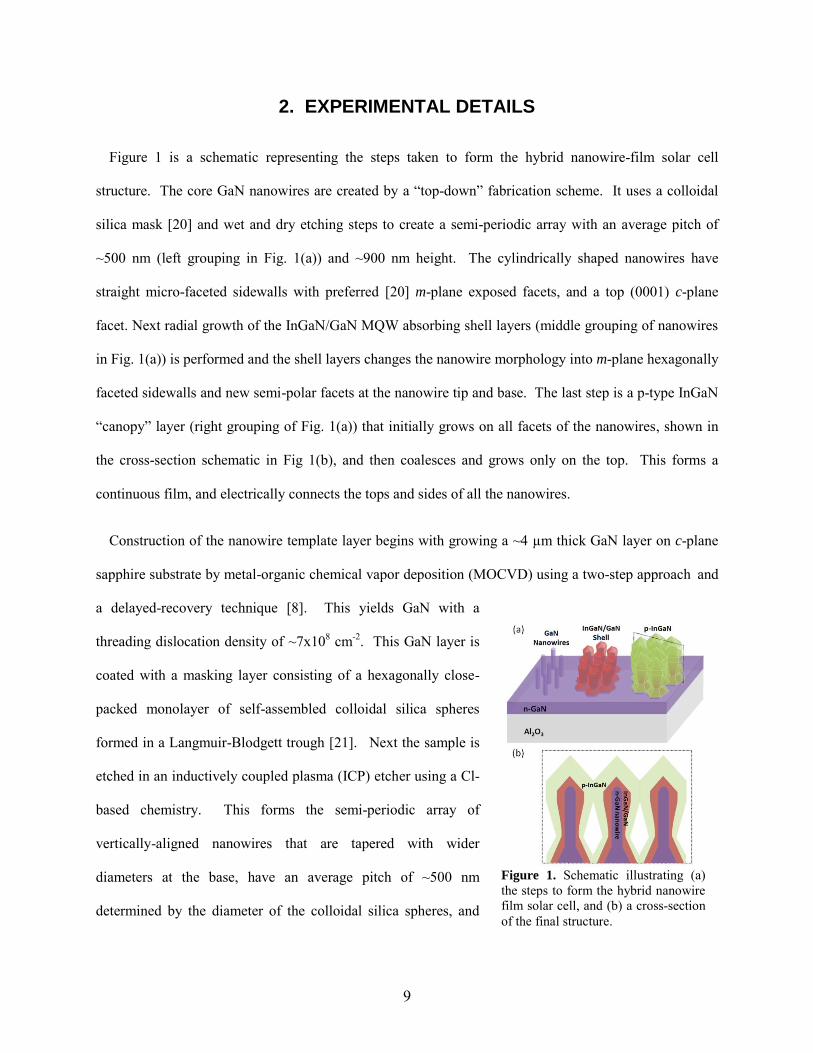
2. EXPERIMENTAL DETAILS
Figure 1 is a schematic representing the steps taken to form the hybrid nanowire-film solar cell
structure. The core GaN nanowires are created by a “top-down” fabrication scheme. It uses a colloidal
silica mask [20] and wet and dry etching steps to create a semi-periodic array with an average pitch of
~500 nm (left grouping in Fig. 1(a)) and ~900 nm height. The cylindrically shaped nanowires have
straight micro-faceted sidewalls with preferred [20] m-plane exposed facets, and a top (0001) c-plane
facet. Next radial growth of the InGaN/GaN MQW absorbing shell layers (middle grouping of nanowires
in Fig. 1(a)) is performed and the shell layers changes the nanowire morphology into m-plane hexagonally
faceted sidewalls and new semi-polar facets at the nanowire tip and base. The last step is a p-type InGaN
“canopy” layer (right grouping of Fig. 1(a)) that initially grows on all facets of the nanowires, shown in
the cross-section schematic in Fig 1(b), and then coalesces and grows only on the top. This forms a
continuous film, and electrically connects the tops and sides of all the nanowires.
Construction of the nanowire template layer begins with growing a ~4 µm thick GaN layer on c-plane
sapphire substrate by metal-organic chemical vapor deposition (MOCVD) using a two-step approach and
a delayed-recovery technique [8]. This yields GaN with a
threading dislocation density of ~7x108 cm-2. This GaN layer is
coated with a masking layer consisting of a hexagonally close-
packed monolayer of self-assembled colloidal silica spheres
formed in a Langmuir-Blodgett trough [21]. Next the sample is
etched in an inductively coupled plasma (ICP) etcher using a Cl-
based chemistry. This forms the semi-periodic array of
vertically-aligned nanowires that are tapered with wider
diameters at the base, have an average pitch of ~500 nm
determined by the diameter of the colloidal silica spheres, and
Figure 1. Schematic illustrating (a) the steps to form the hybrid nanowire film solar cell, and (b) a cross-section of the final structure.
10
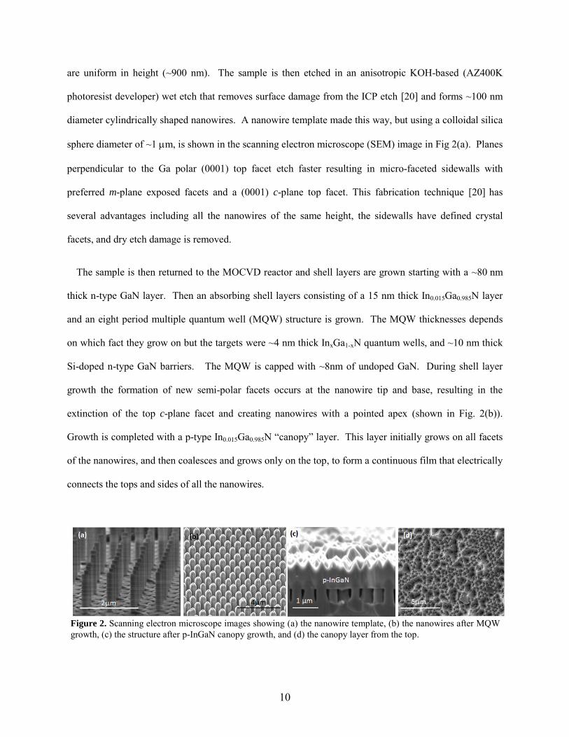
are uniform in height (~900 nm). The sample is then etched in an anisotropic KOH-based (AZ400K
photoresist developer) wet etch that removes surface damage from the ICP etch [20] and forms ~100 nm
diameter cylindrically shaped nanowires. A nanowire template made this way, but using a colloidal silica
sphere diameter of ~1 m, is shown in the scanning electron microscope (SEM) image in Fig 2(a). Planes
perpendicular to the Ga polar (0001) top facet etch faster resulting in micro-faceted sidewalls with
preferred m-plane exposed facets and a (0001) c-plane top facet. This fabrication technique [20] has
several advantages including all the nanowires of the same height, the sidewalls have defined crystal
facets, and dry etch damage is removed.
The sample is then returned to the MOCVD reactor and shell layers are grown starting with a ~80 nm
thick n-type GaN layer. Then an absorbing shell layers consisting of a 15 nm thick In0.015Ga0.985N layer
and an eight period multiple quantum well (MQW) structure is grown. The MQW thicknesses depends
on which fact they grow on but the targets were ~4 nm thick InxGa1-xN quantum wells, and ~10 nm thick
Si-doped n-type GaN barriers. The MQW is capped with ~8nm of undoped GaN. During shell layer
growth the formation of new semi-polar facets occurs at the nanowire tip and base, resulting in the
extinction of the top c-plane facet and creating nanowires with a pointed apex (shown in Fig. 2(b)).
Growth is completed with a p-type In0.015Ga0.985N “canopy” layer. This layer initially grows on all facets
of the nanowires, and then coalesces and grows only on the top, to form a continuous film that electrically
connects the tops and sides of all the nanowires.
Figure 2. Scanning electron microscope images showing (a) the nanowire template, (b) the nanowires after MQW growth, (c) the structure after p-InGaN canopy growth, and (d) the canopy layer from the top.
11
Figure 2(c) shows a cross-sectional SEM image of the completed structure. The p-type InGaN layer
coalesces the structure, leaving embedded air voids between nanowires which enhance light scattering
and absorption within the structure. A top view of the surface is shown in the SEM image of Fig. 2(d).
It is off-white in appearance, consisting of a dense array of V-defects formed by the intersection of the top
{10-11} facets of the nanowires after coalescence. This is typical of thick, lower temperature growth of
III-nitrides [22]. The nanowire array has some short range hexagonal ordering and manifests in the
regular hexagonal shaped features of the surface seen in some areas, most notably at the upper right in
Fig. 2(d). The nanowires are centered below the apexes of the faceted surface.
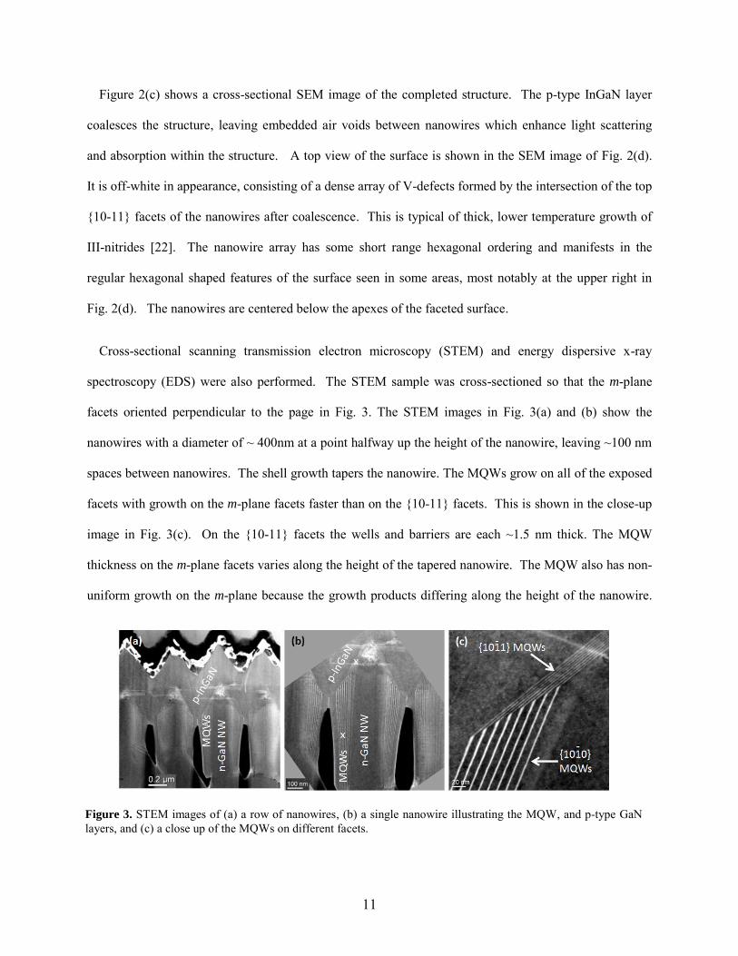
Cross-sectional scanning transmission electron microscopy (STEM) and energy dispersive x-ray
spectroscopy (EDS) were also performed. The STEM sample was cross-sectioned so that the m-plane
facets oriented perpendicular to the page in Fig. 3. The STEM images in Fig. 3(a) and (b) show the
nanowires with a diameter of ~ 400nm at a point halfway up the height of the nanowire, leaving ~100 nm
spaces between nanowires. The shell growth tapers the nanowire. The MQWs grow on all of the exposed
facets with growth on the m-plane facets faster than on the {10-11} facets. This is shown in the close-up
image in Fig. 3(c). On the {10-11} facets the wells and barriers are each ~1.5 nm thick. The MQW
thickness on the m-plane facets varies along the height of the tapered nanowire. The MQW also has non-
uniform growth on the m-plane because the growth products differing along the height of the nanowire.
Figure 3. STEM images of (a) a row of nanowires, (b) a single nanowire illustrating the MQW, and p-type GaN layers, and (c) a close up of the MQWs on different facets.
12
This creates faster growth at the top of the nanowire sidewalls compared to the bottom. At the top the
well and barrier thicknesses are ~2.5nm and ~9nm respectively. At the bottom of the MQW is thinner,
and the innermost wells and barriers are thicker than the outermost wells and barriers. The innermost
well and barrier is ~2.5 nm and ~5.5 nm thick respectively while the outermost well and barrier is ~1.8nm
and ~3nm thick respectively. This change in MQW thickness is due to reduced transport of gas phase
reactants as the opening between nanowires is pinched off during growth. EDS reveals the indium
incorporation in quantum wells is also different on the sidewall and {10-11} facets with x~0.33 (±5%) on
the m-planes compared to x~0.22 (±5%) on the {10-11} planes. The difference in indium composition on
the two different planes has also been observed in planar material [25]. Lastly, the p-type InGaN layer
extends down along the nanowire sidewalls, allowing for the capture carriers generated by light
absorption in the m-plane MQWs.
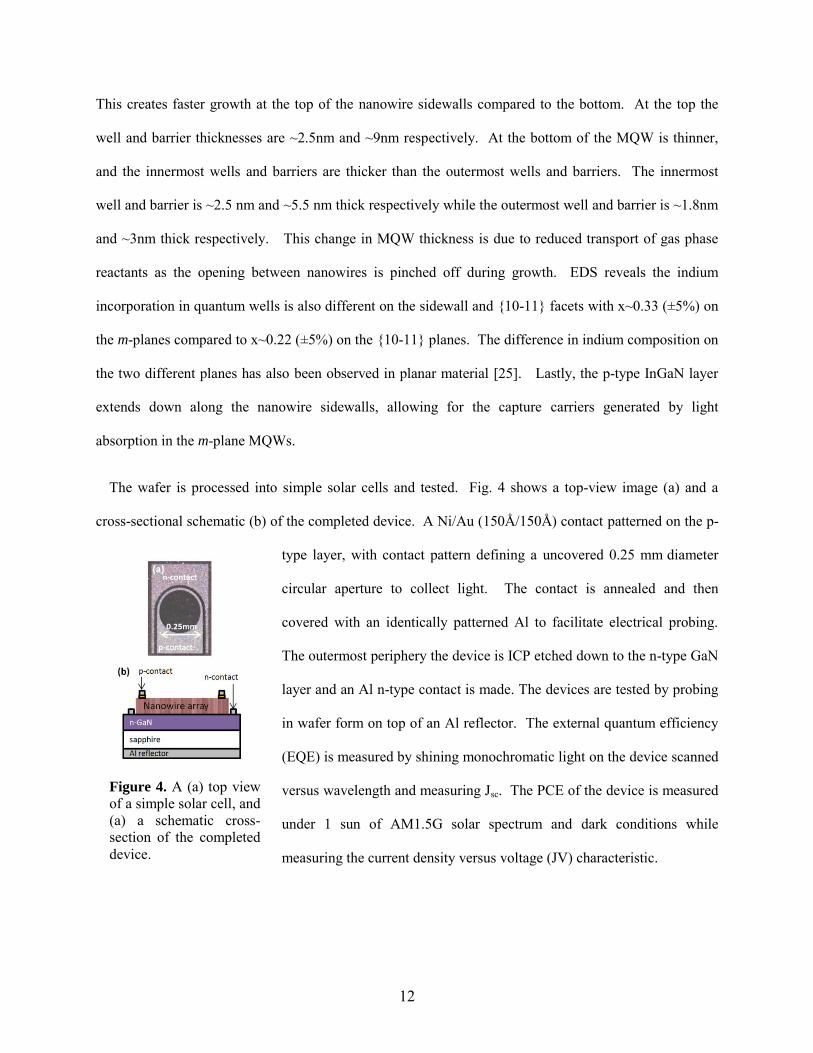
The wafer is processed into simple solar cells and tested. Fig. 4 shows a top-view image (a) and a
cross-sectional schematic (b) of the completed device. A Ni/Au (150Å/150Å) contact patterned on the p-
type layer, with contact pattern defining a uncovered 0.25 mm diameter
circular aperture to collect light. The contact is annealed and then
covered with an identically patterned Al to facilitate electrical probing.
The outermost periphery the device is ICP etched down to the n-type GaN
layer and an Al n-type contact is made. The devices are tested by probing
in wafer form on top of an Al reflector. The external quantum efficiency
(EQE) is measured by shining monochromatic light on the device scanned
versus wavelength and measuring Jsc. The PCE of the device is measured
under 1 sun of AM1.5G solar spectrum and dark conditions while
measuring the current density versus voltage (JV) characteristic.
Figure 4. A (a) top view of a simple solar cell, and (a) a schematic cross-section of the completed device.
13
3. RESULTS AND DISCUSSION
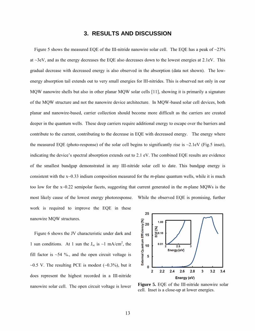
Figure 5 shows the measured EQE of the III-nitride nanowire solar cell. The EQE has a peak of ~23%
at ~3eV, and as the energy decreases the EQE also decreases down to the lowest energies at 2.1eV. This
gradual decrease with decreased energy is also observed in the absorption (data not shown). The low-
energy absorption tail extends out to very small energies for III-nitrides. This is observed not only in our
MQW nanowire shells but also in other planar MQW solar cells [11], showing it is primarily a signature
of the MQW structure and not the nanowire device architecture. In MQW-based solar cell devices, both
planar and nanowire-based, carrier collection should become more difficult as the carriers are created
deeper in the quantum wells. These deep carriers require additional energy to escape over the barriers and
contribute to the current, contributing to the decrease in EQE with decreased energy. The energy where
the measured EQE (photo-response) of the solar cell begins to significantly rise is ~2.1eV (Fig.5 inset),
indicating the device’s spectral absorption extends out to 2.1 eV. The combined EQE results are evidence
of the smallest bandgap demonstrated in any III-nitride solar cell to date. This bandgap energy is
consistent with the x~0.33 indium composition measured for the m-plane quantum wells, while it is much
too low for the x~0.22 semipolar facets, suggesting that current generated in the m-plane MQWs is the
most likely cause of the lowest energy photoresponse. While the observed EQE is promising, further
work is required to improve the EQE in these
nanowire MQW structures.
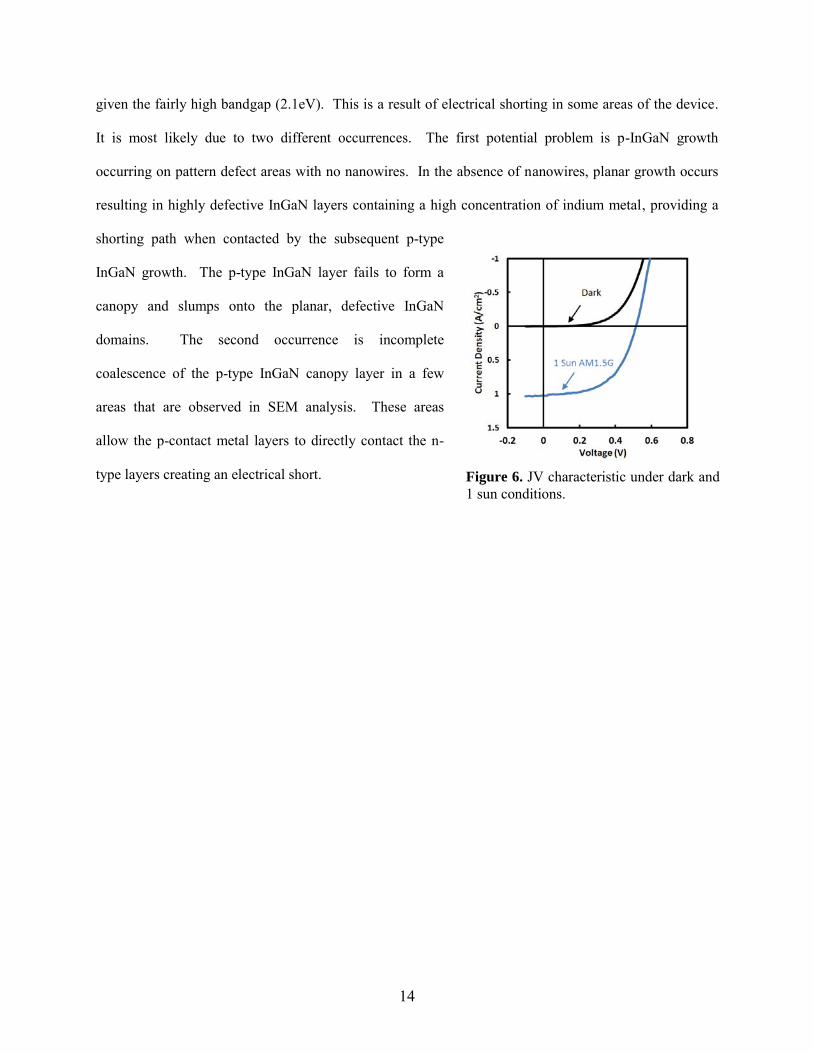
Figure 6 shows the JV characteristic under dark and
1 sun conditions. At 1 sun the Jsc is ~1 mA/cm2, the
fill factor is ~54 %., and the open circuit voltage is
~0.5 V. The resulting PCE is modest (~0.3%), but it
does represent the highest recorded in a III-nitride
nanowire solar cell. The open circuit voltage is lower
Figure 5. EQE of the III-nitride nanowire solar cell. Inset is a close-up at lower energies.
14
given the fairly high bandgap (2.1eV). This is a result of electrical shorting in some areas of the device.
It is most likely due to two different occurrences. The first potential problem is p-InGaN growth
occurring on pattern defect areas with no nanowires. In the absence of nanowires, planar growth occurs
resulting in highly defective InGaN layers containing a high concentration of indium metal, providing a
shorting path when contacted by the subsequent p-type
InGaN growth. The p-type InGaN layer fails to form a
canopy and slumps onto the planar, defective InGaN
domains. The second occurrence is incomplete
coalescence of the p-type InGaN canopy layer in a few
areas that are observed in SEM analysis. These areas
allow the p-contact metal layers to directly contact the n-
type layers creating an electrical short.
Figure 6. JV characteristic under dark and 1 sun conditions.
15
4. CONCLUSION
For the first time solar cells consisting of a vertically integrated array of core-shell III-nitride nanowires
are demonstrated. The novel hybrid nanowire-film structure is created by radial growth on an n-type
array of GaN nanowires formed by simple wet and dry etching. The p-type InGaN canopy layer
electrically connects the nanowires and allows for simple fabrication techniques. The nanowire structure
has benefits such as higher indium composition InGaN layers and more efficient carrier collection and
enhanced light trapping. The solar cell exhibits a photoresponse out to 2.1eV, the lowest bandgap of any
III-nitride solar cell so far, and the power conversion efficiency is the highest recorded for a III-nitride
nanowire solar cell.
16
17
5. REFERENCES 1. Krames, M.R., et al., Status and future of high-power light-emitting diodes for solid-state
lighting. Journal of Display Technology, 2007. 3(2): p. 160-175. 2. Trybus, E., et al., Characteristics of InGaN designed for photovoltaic applications. Physica
Status Solidi C - Current Topics in Solid State Physics, Vol 5, No 6, 2008. 5(6): p. 1843-1845.
3. Wu, J., et al., Superior radiation resistance of In1-xGaxN alloys: Full-solar-spectrum
photovoltaic material system. Journal of Applied Physics, 2003. 94(10): p. 6477-6482. 4. Muth, J.F., et al., Absorption coefficient, energy gap, exciton binding energy, and
recombination lifetime of GaN obtained from transmission measurements. Applied Physics Letters, 1997. 71(18): p. 2572-2574.
5. Ponce, F.A., et al., Microstructure and electronic properties of InGaN alloys. Physica Status Solidi B-Basic Research, 2003. 240(2): p. 273-284.
6. Neufeld, C.J., et al., Effect of doping and polarization on carrier collection in InGaN
quantum well solar cells. Applied Physics Letters, 2011. 98(24). 7. Wierer, J.J., A.J. Fischer, and D.D. Koleske, The impact of piezoelectric polarization and
nonradiative recombination on the performance of (0001) face GaN/InGaN photovoltaic
devices. Applied Physics Letters, 2010. 96(5): p. 051107. 8. Koleske, D.D., et al., GaN decomposition in H-2 and N-2 at MOVPE temperatures and
pressures. Journal of Crystal Growth, 2001. 223(4): p. 466-483. 9. Wu, X.H., et al., Structural origin of V-defects and correlation with localized excitonic
centers in InGaN/GaN multiple quantum wells. Applied Physics Letters, 1998. 72(6): p. 692-694.
10. Dahal, R., et al., InGaN/GaN multiple quantum well concentrator solar cells. Applied Physics Letters, 2010. 97(7).
11. Farrell, R.M., et al., High quantum efficiency InGaN/GaN multiple quantum well solar cells
with spectral response extending out to 520 nm. Applied Physics Letters, 2011. 98(20). 12. Lauhon, L.J., et al., Epitaxial core-shell and core-multishell nanowire heterostructures.
Nature, 2002. 420(6911): p. 57-61. 13. Dong, Y.J., et al., Coaxial Group III-Nitride Nanowire Photovoltaics. Nano Letters, 2009.
9(5): p. 2183-2187. 14. Li, Q.M. and G.T. Wang, Strain influenced indium composition distribution in GaN/InGaN
core-shell nanowires. Applied Physics Letters, 2010. 97(18). 15. Kayes, B.M., et al., Radial PN junction nanorod solar cells: Device physics principles and
routes to fabrication in silicon. Conference Record of the Thirty-First IEEE Photovoltaic Specialists Conference - 2005, 2005: p. 55-58.
16. Kelzenberg, M.D., et al., Enhanced absorption and carrier collection in Si wire arrays for
photovoltaic applications (vol 9, pg 239, 2010). Nature Materials, 2010. 9(4): p. 368-368. 17. Yu, Z.F., A. Raman, and S.H. Fan, Fundamental limit of light trapping in grating structures.
Optics Express, 2010. 18(19): p. A366-A380. 18. Colombo, C., et al., Gallium arsenide p-i-n radial structures for photovoltaic applications.
Applied Physics Letters, 2009. 94(17). 19. Goto, H., et al., Growth of Core-Shell InP Nanowires for Photovoltaic Application by
20. Li, Q.M., et al., Optical performance of top-down fabricated InGaN/GaN nanorod light
emitting diode arrays. Optics Express, 2011. 19(25): p. 25528-25534. 21. Li, Q.M., J.J. Figiel, and G.T. Wang, Dislocation density reduction in GaN by dislocation
filtering through a self-assembled monolayer of silica microspheres. Applied Physics Letters, 2009. 94(23).
22. Scholz, F., et al., In incorporation efficiency and composition fluctuations in MOVPE grown
GaInN/GaN hetero structures and quantum wells. Materials Science and Engineering B-Solid State Materials for Advanced Technology, 1997. 50(1-3): p. 238-244.
19
20
DISTRIBUTION 1 MS1086 Dan Barton 01123(electronic copy) 1 MS1086 Bob Biefeld 01126(electronic copy) 1 MS0899 Technical Library 9536 (electronic copy) 1 MS0359 D. Chavez, LDRD Office 1911