Image Sensor Technology for Beam Instrumentation R. Jung CERN, CH1211 Geneva 23, Switzerland Abstract. Beam monitoring using cameras has evolved from qualitative beam observation to precision measurement. After a description of the two main TV standards, various sensors including TV tubes (Vidicon), solid state sensors (Interline and Frame transfer CCDs, CMOS and CID X-Y matrices), and Fast Shutter/Intensifiers of the MCP type are reviewed. Comparative resolution measurements for the various sensors are given. The two types of sensor acquisition hardware, “frame grabbers” and “digital cameras,” am described Finally, special image processing requirements for beam instrumentation are reviewed, including radiation hardness, spectral sensitivity, fast acquisition, and enlarged dynamic range. INTRODUCTION Television cameras have been used since the early days of accelerators for beam observation. The main application was for a long time the observation of screens for beam steering purposes through transfer lines and for the first turn around circular machines. With the construction of lepton machines producing enough synchrotron radiation, and high intensity proton storage rings, the use of TV based monitors was extended to the measurement of beam dimensions for machine optimization and luminosity estimation. Instruments of this type were developed in several laboratories in the 1970s with tube TV cameras and included some form of digitization and numerical processing for beam size extraction. Despite the usefulness of these instruments, it took a certain number of years to have them accepted as precision instruments. The introduction of the CCD sensor, with its more than 100,000 cells having silicon- engraved precision of a few microns, came to maturity in the early eighties, just in time for LEP. Camera-based beam monitors have now acquired a competitive position in beam instrumentation and are recognized as indispensable instruments in accelerators. The users now have maximum expectations from them. The recent improvements of CMOS sensors and the interest of industry and universities in machine vision have induced enormous progress in the field and there is now a wide variety of hardware and software available, some of which is directly useful for beam instrumentation.
Transcript
Image Sensor Technology for Beam Instrumentation
R. Jung
CERN, CH1211 Geneva 23, Switzerland
Abstract. Beam monitoring using cameras has evolved from qualitative beam observation to precision measurement. After a description of the two main TV standards, various sensors including TV tubes (Vidicon), solid state sensors (Interline and Frame transfer CCDs, CMOS and CID X-Y matrices), and Fast Shutter/Intensifiers of the MCP type are reviewed. Comparative resolution measurements for the various sensors are given. The two types of sensor acquisition hardware, “frame grabbers” and “digital cameras,” am described Finally, special image processing requirements for beam instrumentation are reviewed, including radiation hardness, spectral sensitivity, fast acquisition, and enlarged dynamic range.
INTRODUCTION
Television cameras have been used since the early days of accelerators for beam observation. The main application was for a long time the observation of screens for beam steering purposes through transfer lines and for the first turn around circular machines. With the construction of lepton machines producing enough synchrotron radiation, and high intensity proton storage rings, the use of TV based monitors was extended to the measurement of beam dimensions for machine optimization and luminosity estimation. Instruments of this type were developed in several laboratories in the 1970s with tube TV cameras and included some form of digitization and numerical processing for beam size extraction. Despite the usefulness of these instruments, it took a certain number of years to have them accepted as precision instruments. The introduction of the CCD sensor, with its more than 100,000 cells having silicon- engraved precision of a few microns, came to maturity in the early eighties, just in time for LEP.
Camera-based beam monitors have now acquired a competitive position in beam instrumentation and are recognized as indispensable instruments in accelerators. The users now have maximum expectations from them.
The recent improvements of CMOS sensors and the interest of industry and universities in machine vision have induced enormous progress in the field and there is now a wide variety of hardware and software available, some of which is directly useful for beam instrumentation.
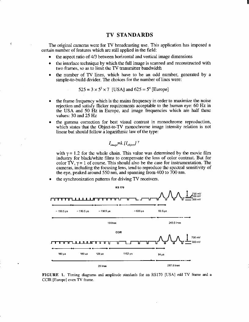
TV STANDARDS
The original cameras were for TV broadcasting use. This application has imposed a certain number of features which are still applied in the field:
l the aspect ratio of 4/3 between horizontal and vertical image dimensions l the interlace technique by which the full image is scanned and reconstructed with
two frames, so as to limit the TV transmitter bandwidth l the number of TV lines, which have to be an odd number, generated by a
simple-to-build divider, The choices for the number of lines were:
525 = 3 x 5* x 7 [USA] and 625 = 54 [Europe]
l the frame frequency which is the mains frequency in order to maximize the noise rejection and satisfy flicker requirements acceptable to the human eye: 60 Hz in the USA and 50 Hz in Europe, and image frequencies which are half these values: 30 and 25 Hz
l the gamma correction for best visual contrast in monochrome reproduction, which states that the Object-to-TV monochrome image intensity relation is not linear but should follow a logarithmic law of the type:
limage=k [‘object] ’
with y = 1.2 for the whole chain. This value was determined by the movie fihn industry for black/white films to compensate the loss of color contrast. But for color TV, y= 1 of course. This should also be the case for instrumentation. The cameras, including the focusing lens, tend to reproduce the spectral sensitivity of the eye, peaked around 550 nm, and spanning from 400 to 700 nm.
l the synchronization patterns for driving TV receivers.
RS 170
- 190.5 ps -19osps -1905p - 635 ps 63.5 ps
. ---
19 lines 243.5 lines
CCIR
700 mv
JIIU-ulIInnnIluu~ UJ u u . . u &&A.$ 300 mV -
. .
160~s 160 ps 128 ps 1152 1s MPS
l --. -,
25 lines 287.5 lines
FIGURE 1. Timing diagrams and amplitude standards for an RS170 [USA] cdd TV frame and a CCIR [Europe] even TV frame.
The previous features were translated into TV standards, RS170 for the USA and CCIR for Europe, similar to which all analog TV cameras comply. As can be seen in Figure 1, these standards are close to each other. The signal delivered by a TV camera is called the composite video signal. Only the so-called digital cameras do not comply to these TV standards.
A typical block diagram for a complete system is given in Figure 2.
. TV Mode TV sequencer
Integrate 8 Scan control
1
Signal Mixer , . TV mode
w Composite Video f I
Image Image , senscf senscf
Signal - Process3 .
NonTVmode . Sereor signal
b Timing
Sequencer Sensor control
FIGURE 2. Block diagram of a complete camera system.
TUBE CAMERAS
The tube cameras were the first available image sensors. The only interest in them nowadays is for their radiation resistance, and hence the whole camera has to be made with tubes, including image sensor, amplifiers, and other active elements. Only the Vidicon (Figure 3), the most popular of them, and the SIT image sensors will be mentioned.
I I I I
Video OUT
FIGURE 3. Schematic view of a Vidicon TV tube with deflection coils and lens.
The Vidicon sensor is an evacuated tube with a photoconductive target on which the scene of interest is imaged. The conductivity of the target is a replica of the scene illumination. The face of the target towards the input window is coated with a transparent metallic layer connected to the signal output of the tube. A low-energy electron beam orthogonally scans the inner surface of the target and the video output signal follows the illumination of the scene. The electron beam is focused with a solenoid coil and its deflection is controlled by magnetic fields generated by the deflection coils. The image is scanned in the usual raster scan every second line. The Vidicon has a sensitivity better than the eye in approximately the same spectral range, a gamma of around 0.7, and a rather long remanence of several frames. It has a very high radiation resistance.
The SIT (Silicon Intensified Target) is a two-stage tube. The first stage is an intensifier using a photocathode onto which the scene is imaged. The electrons emitted by it are accelerated to a silicon target made of tightly spaced p-n diodes where the accelerated electrons create electron-hole pairs. A scanning electron beam neutralizes the holes which are collected on the scanning side of the target and again generates the video signal, which is the replica of the scene. Due to the two stages, a gain of 1000 or more can be achieved with respect to the Vidicon. These tubes have a high sensitivity, a spectral range depending on the photocathode type, in general extended towards the infrared up to 800 nm, a low remanence, and a gamma of 1. The silicon target makes these tubes less radiation-resistant than the Vidicon.
Cameras of this type are used in high radiation areas where the integrated doses go above lo4 Gy (lo6 rad). They suffer from external magnetic fields, which occur in pulsed machines and necessitate magnetic shielding. As for any standard TV cameras, they can be connected to TV monitors for direct observation and the composite video signal can be digitized for further processing by the standard “frame grabbers.” Due to the scanning mechanism, there is a time difference of one mains period between top and bottom of the same frame, and between two adjacent TV lines. This is in general not a severe limitation in usual instrumentation applications where time resolution is not a requirement. Their spatial resolution has been measured and is good (see Figure 15).
SOLID STATE CAMERAS
Solid-state sensors of the CMOS type appeared in the late sixties and CCDs in the early seventies. Despite its later appearance, the CCD sensor developed faster to a mature technology and is presently the leading technology. It is mainly the field of the large solid-state electronics companies and for the moment dominates scientific-type applications. CMOS is catching up rapidly. Because of its simpler technology, similar to that used for producing RAM, it is a field open to many companies, of all sizes, including university laboratory spin-offs. With this technology, it is possible to integrate, on the same chip, the image sensor and signal processing functions, including ADCs and digital processing.
Linear sensors exist mainly in CCD technology. They are a simplified version of the area sensor. They have many commercial applications and can be interesting in beam instrumentation applications where one-dimensional information is of interest and where readout speed is the main concern. Only area sensors will be further considered.
Both CCD and CMOS sensors are based on the photoelectric effect in silicon. When a photon of an appropriate wavelength (in general between 200 and 1000 nm) hits silicon, it generates an electron-hole pair. If an electric field is present, the electron and the hole are separated and charge can accumulate, proportional to the number of incident
photons, and so reproduce the scene imaged onto the detector if a proper X-Y structure is present. Each basic element, defining the granularity of the sensor, is called a pixel (picture element). An image is composed of typically 400 x 300 pixels, with dimensions of the order of 10 to 25 pm. Two types of techniques can generate the pixel structure: a MOS capacitor or a p-n junction (see Figure 4).
Photon Ph
FIGURE 4. MOS capacitor and p-n diode structures for image sensors.
A positive bias applied onto the MOS gate creates a depletion region where the electrons are accumulated, whereas the holes disappear in the substrate. Electrons created in the substrate are either attracted to the depletion region or are lost, if they are created too far from it. This process is characterized by the Quantum Efficiency, having a maximum variance between 40% and 80%, depending on the technology. The electrons are accumulated for a certain length of time, in order to generate enough signal at read-out. In TV type applications, this integration length is limited by the mains frequency. Maximum accumulated charges are typically of the order of 300,000 electrons. As in any semiconductor device, there are also thermally generated electron- hole pairs which add to the signal and generate so-called dark current. In order to improve the sensitivity and reduce the noise, the sensors can be cooled, as the thermal current in silicon is divided by two every 8 K. The cooling ranges from tens of degrees, achieved with Peltier cells, down to cryogenic cooling in extreme cases.
The readout mode of the accumulated charges will define the type of sensor: CCD or X-Y matrix read-out. The solid-state sensors which have been used as examples in this tutorial are presented in Figure 5.
FIGURE 5. Solid state sensor cameras. From left to right: frame transfer and interline CCDs, CID, and CMOS XY sensors. The last one is a complete TV system.
CCD Sensors
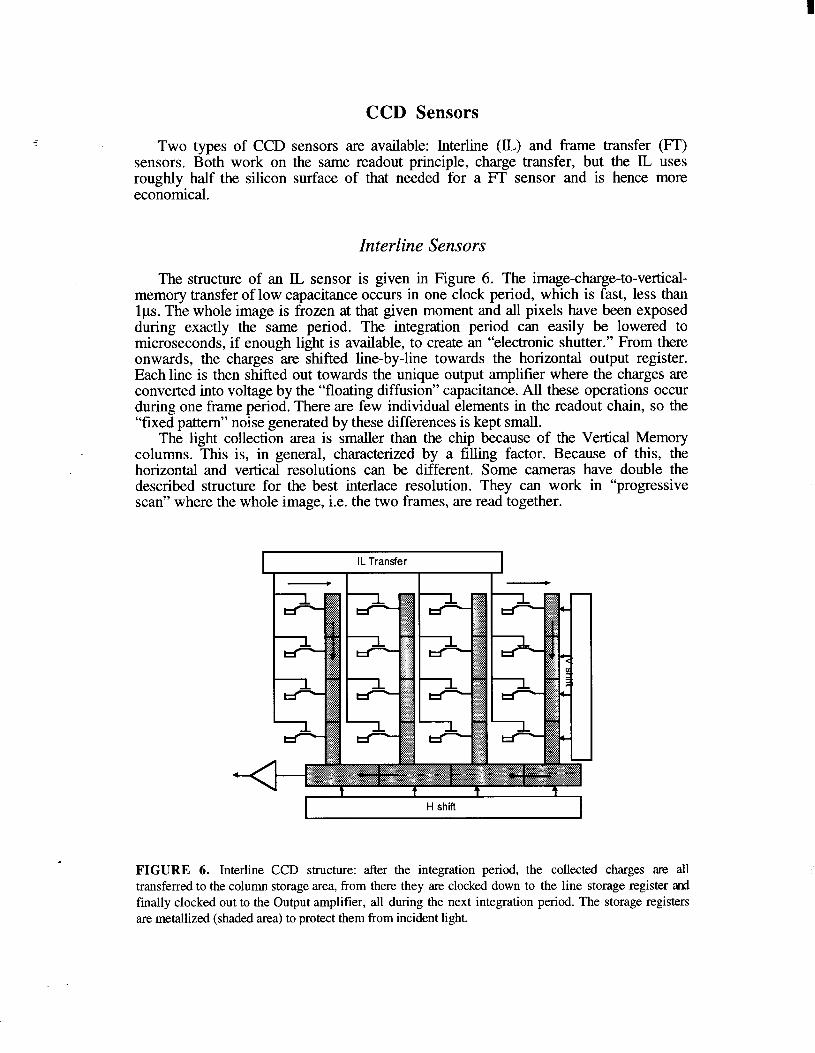
Two types of CCD sensors are available: Interline (IL) and frame transfer (ET) sensors. Both work on the same readout principle, charge transfer, but the IL uses roughly half the silicon surface of that needed for a ET sensor and is hence more economical.
Interline Sensors
The structure of an IL sensor is given in Figure 6. The image-charge-to-vertical- memory transfer of low capacitance occurs in one clock period, which is fast, less than 1~s. The whole image is frozen at that given moment and all pixels have been exposed during exactly the same period. The integration period can easily be lowered to microseconds, if enough light is available, to create an “electronic shutter.” From there onwards, the charges are shifted line-by-line towards the horizontal output register. Each line is then shifted out towards the unique output amplifier where the charges are converted into voltage by the “floating diffusion” capacitance. All these operations occur during one frame period. There are few individual elements in the readout chain, so the “fixed pattern” noise generated by these differences is kept small.
The light collection area is smaller than the chip because of the Vertical Memory columns. This is, in general, characterized by a filling factor. Because of this, the horizontal and vertical resolutions can be different. Some cameras have double the described structure for the best interlace resolution. They can work in “progressive scan” where the whole image, i.e. the two frames, are read-together.
IL Transfer
t I
I I
I
I H shift
FIGURE 6. Interline CCD structure: after the integration period, the collected charges are all transferred to the column storage area, from there they are clocked down to the line storage register and finally clocked out to the Output amplifier, all during the next integration period. The storage registers are metallized (shaded area) to protect them from incident light.
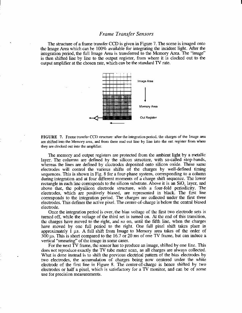
Frame Transfer Sensors
The structure of a frame transfer CCD is given in Figure 7. The scene is imaged onto the Image Area which can be 100% available for integrating the incident light. After the integration period, the full Image Area is transferred to the Memory Area. The “image” is then shifted line by line to the output register, from where it is clocked out to the output amplifier at the chosen rate, which can be the standard TV rate.
4-
mage Area
M emery Area
Out Register
FIGURE 7. Frame transfer CCD structure: after the integration period, the charges of the Image area are shifted into the Memory area, and from there read out line by line into the out register from where they are clocked out into the amplifier.
The memory and output registers are protected from the ambient light by a metallic layer. The columns are defined by the silicon structure, with so-called stop-bands, whereas the lines are defined by electrodes deposited onto silicon oxide. These same electrodes will control the various shifts of the charges by well-defined timing sequences. This is shown in Fig, 8 for a four-phase system, corresponding to a column during integration and at four different moments of a charge shift sequence. The lower rectangle in each line corresponds to the silicon substrate. Above it is an SiO, layer, and above that, the polysilicon electrode structure, with a four-fold periodicity. The electrodes, which are positively biased, are represented in black. The first line corresponds to the integration period. The charges are collected under the first three electrodes. This defines the active pixel. The center-of-charge is below the central biased electrode.
Once the integration period is over, the bias voltage of the first two electrode sets is turned off, while the voltage of the third set is turned on. At the end of this transition, the charges have moved to the right, and so on, until the fifth line, when the charges have moved by one full period to the right. One full pixel shift takes place in approximately 1 us. A full shift from Image to Memory area takes of the order of 300 us. This is short compared to the 16.7 or 20 ms of one TV frame, but can induce a vertical “smearing” of the image in some cases.
For the next TV frame, the sensor has to produce an image, shifted by one line. This does not reproduce exactly the TV tube raster scan, as all charges are always collected. What is done instead is to shift the previous electrical pattern of the bias electrodes by two electrodes, the accumulation of charges being now centered under the white electrode of the first line in Figure 8. The center-of-charge is hence shifted by two electrodes or half a pixel, which is satisfactory for a TV monitor, and can be of some use for precision measurements.
FIGURE 8. CCD structure and timing sequence for a four-phase sensor for the integration period and a complete shift of one pixel. The biased electrodes are in black, and the charge-collection areas are the shaded areas below the biased electrodes. During the integration, one electrode (gray shaded) is biased at a smaller voltage.
Frame transfer CCDs have, in principle, the best sensitivity, as the full silicon area is available for photon-to-charge conversion. They have for the same reason a good resolution for a given pixel size, a high output signal and a good uniformity. Their disadvantage comes from the many charge shifts, typically from 300 to 1000 from the closest to the farthest pixel. Figure 9 depicts a measurement of charge transfer efficiencies (CTE) made at different pixel readout frequencies. It should be pointed out that the individual shifts are very efficient: in this example from 99.97% to 99.99%.
80 -- C 70 -- T E
400 600
Shift [pixel]
I 800 1000
FIGURE 9. Measured Charge Transfer Efficiencies [CTE] as a function of readout frequency. The normal TV readout frequency is close to 7 MHz.
The lower spectral sensitivity of the CCD is limited by the electrode and protection window transmittances to wavelengths longer than 400 nm. To go below these wavelengths, either UV scintillator coatings or back-illuminated CCDs are used. The coated CCDs are a much cheaper solution, but their resolution is limited by the emission angle of the coating. The back-illuminated CCD has a normal CCD structure, illuminated from the back. The silicon has to be thinned so as to avoid the recombination of the photon-generated electrons with holes before reaching the collecting potential well. The efficiency can be the double of an ordinary CCD. This process results of course in a higher cost.
X-Y CMOS and CID sensors
In a CMOS sensor, each pixel is comprised of a photodiode with a MOS switch and is individually addressable in the following way. All gates on one line are connected to a horizontal register and all drains of the MOS transistors in one column are connected to a sense line connected through a transistor to the video output amplifier (see Figure 10). Each pixel is read sequentially once per frame.
Some more elaborate detectors of this type use several MOS transistors. Others, rather than sequentially reading the integrated charge, sequentially integrate the current generated by each photodiode for a given time. The most elaborate use a log amplifier in order to achieve the highest dynamic range.
X select
FIGURE 10. X-Y matrix image sensor: the Y selection register selects a pixel row, of which the X selection register selects a pixel at the intersection of both lines, which is connected to the output amplifier.
The major disadvantages of this architecture are a potential lower sensitivity due to the smaller photo-active surface available and a fixed-pattern noise due to the differences in the individual transistors. These disadvantages are disappearing rapidly as the technology progresses and as more signal processing functions are incorporated on the
sensor chip. Such incorporation is easy in this technology. Recent sensors have a performance comparable to or even better than the best Frame transfer CCDs (see Figure 15). The possibility of integrating signal processing circuits on the silicon of the sensors is a big advantage. The suppression of the fixed-pattern noise by double correlated sampling is one of the important functions which are available. There can also be an automatic integration time adjustment for best dynamic range with fixed- diaphragm optics. This can be a disadvantage in pulsed-light operation, frequent in accelerator environments, unless precautions are taken. Some of the chips also incorporate an ADC, resulting in a true digital image sensor of small dimension. These components will probably be the dominant image sensors in the next generation.
The CID (Charge Injection Device) is also a sensor of the X-Y type. It is comprised of two MOS .photogates._The charges are read non-destructively when they are shifted from one photogate to the other. Integration can be resumed after readout, in principle, for each pixel individually if the signal level is too low. The charges are discarded before a new integration period by “injection” into the substrate. They are the most radiation- resistant sensors. Unfortunately, these devices are single-sourced.
INTENSIFIERS
An intensifier is a vacuum tube optoelectronic device. It is comprised of a photocathode that emits electrons, a gain mechanism, and a screen transforming the electron flux back to photons. In first generation intensifiers, the gain was given by the electrostatic acceleration of the photoelectrons. It was moderate and the image distortions were not negligible. In the second generation, the gain is given by the multiplication of the electrons by secondary emission in a Multi Channel Plate (MCP) made of many little conductive glass tubes, typically 10 pm in diameter. One electron generates many electrons, which gives the amplification but also degrades the resolution of the device. There can be more than one plate. The principle is given in Figure 11.
Photons IN Broad spectal range
Photons OUT 550 “In
Gating HV Accelerating HV
FIGURE 11. Operating principle of a MCP intensifier.
Third-generation intensifiers have a Gallium Arsenide photocathode in place of the usual multi-alkali photocathode of second generation intensifiers in order to increase the infrared response, which is not of concern in beam instrumentation in general. They will not be considered further here.
The intensifier can be used in DC or pulsed mode. Pulsed intensifiers are used to solve three different problems:
0 not enough light available for a good Signal to Noise ratio
l time resolution by gating the intensifier
l wavelength shifting by proper choice of the photocathode and screen materials: the screen material is chosen for the best match with the sensor spectral sensitivity, and for a decay time compatible with the expected time resolution.
The intensifier is coupled to a CCD or another sensor either by lenses or by direct fiber optic coupling. The latter is the most compact and efficient method.
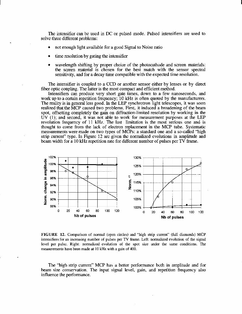
Intensifiers can produce very short gate times, down to a few nanoseconds, and work up to a certain repetition frequency; 10 kHz is often quoted by the manufacturers. The reality is in general less good. In the LEP synchrotron light telescopes, it was soon realized that the MCP caused two problems. First, it induced a broadening of the beam spot, offsetting completely the gain on diffraction-limited resolution by working in the UV (1); and second, it was not able to work for measurement purposes at the LEP revolution frequency of 11 kHz. The last limitation is the most serious one and is thought to come from the lack of electron replacement in the MCP tube. Systematic measurements were made on two types of MCPs: a standard one and a so-called “high strip current” type. In Figure 12 are given the normalized evolutions in amplitude and beam width for a 10 kHz repetition rate for different number of pulses per TV frame.
102% 3 a 100%
.Z E E 98% B .E 96%
El 5
94%
5 92%
G 6 90% z
88%
125%
120% c
E 115% b z
110%
105%
100% +
0 20 40 60 80 100 120 0 20 40 60 80 100 120 Nb of pulses Nb of pulses
FIGURE 12. Comparison of normal (open circles) and “high strip current” (full diamonds) MCP intensifiers for an increasing number of pulses per TV frame. Left: normalized evolution of the signal level per pulse. Right: normalized evolution of the spot size under the same conditions. The measurements have been made at 10 kHz with a gain of 400.
The “high strip current” MCP has a better performance both in amplitude and for beam size conservation. The input signal level, gain, and repetition frequency also influence the performance.
DIGITAL IMAGE ACQUISITION
The direct observation of a beam spot on a TV screen has long been the principal use of camera monitors in beam instrumentation. With the possibility of digitizing the images, a new field was opened for these monitors: the evaluation and monitoring of beam emittances, replacing SEM-Grids in transfer lines and wire scanners in circular machines where light emission was available in sufficient quantity. There are two main ways to digitize an image: either by acquiring the standard TV signal with a “hame grabber,” or by digitizing the pixels individually, which is done by the “digital” or “slow scan” cameras.
Frame Grabbers
A frame grabber takes the standard TV signal (RS170 or CCIR), uses the synchronization signals to start a frame recording and restart a new line, generates (in general) an internal clock, digitizes the video signal with a fast ADC, and stores the result in memory (Figure 13). There is sometimes a synchronization on the actual pixel clock and some pre-processing of the data stored in memory.
Gain
Video IN I Video 8 Sync
b separation
TV standard Sync
extraction & - Clock generation
Flash Frame t ADC Memory
FIGURE 13. Block diagram of a frame grabber.
Most of the frame grabbers use an 8-bit flash ADC, which is adequate for the majority of applications. The digitizing rate is in general half the frame rate, i.e. 30 or 25 Hz. The interface with the digital world is either through a standard bus system or a serial link. The most popular ones are the PC1 bus and the RS 232 or higher performance RS 422 interfaces. A few systems are compatible with the VME standard. The number of available PC1 cards is growing rapidly.
Digital Cameras
A so-called digital camera is comprised of an image sensor and digitizing circuits, delivering to the outside world digital information which is or can be processed further. Being independent of the video standards, the system can be optimized for best performance. As the sensor quality is closer to 12 rather than to 8 bits, these systems start in general at 12 bits and go frequently up to 16 bits, i.e. 65,000 gray levels instead of 256! The price to pay is a slower digitizing frequency or a smaller digitized area, which is particularly well suited to beam instrumentation applications, where the beams are approximate ellipses located in a well known region. For CCD sensors, the digitizer is usually on a different card and takes full control of the sensor, i.e. integration start and stop, image-to-memory transfer and individual pixel read-out. The digitizer can also take a reference dark-level image to subtract from the real image in order to get rid of thermal and fixed pattern noise, and so increase the dynamic range, For CMOS sensors, the pre-processing and ADC can be incorporated on the sensor chip, increasing also the signal-to-noise and dynamic range. The recent progress in this field is remarkable. The data acquisition and bus interface board can contain many processing functions. A typical structure is illustrated in Figure 14.
Clock generation
Gain . . . .
sensor
I
Analog -*e-^^i”” I ADC Frame
.a----.
I I
Video, RGB image 4 Image generator
Digital a Processing
FIGURE 14. Block diagram of a digital camera.
The advantage of these cameras is their better digital data quality, their disadvantage being the lack of a direct video image to follow, in real time, the beam behavior. Some digital systems include image generators for that reason.
SPATIAL RESOLUTION MEASUREMENTS FOR THE VARIOUS SENSOR TYPES
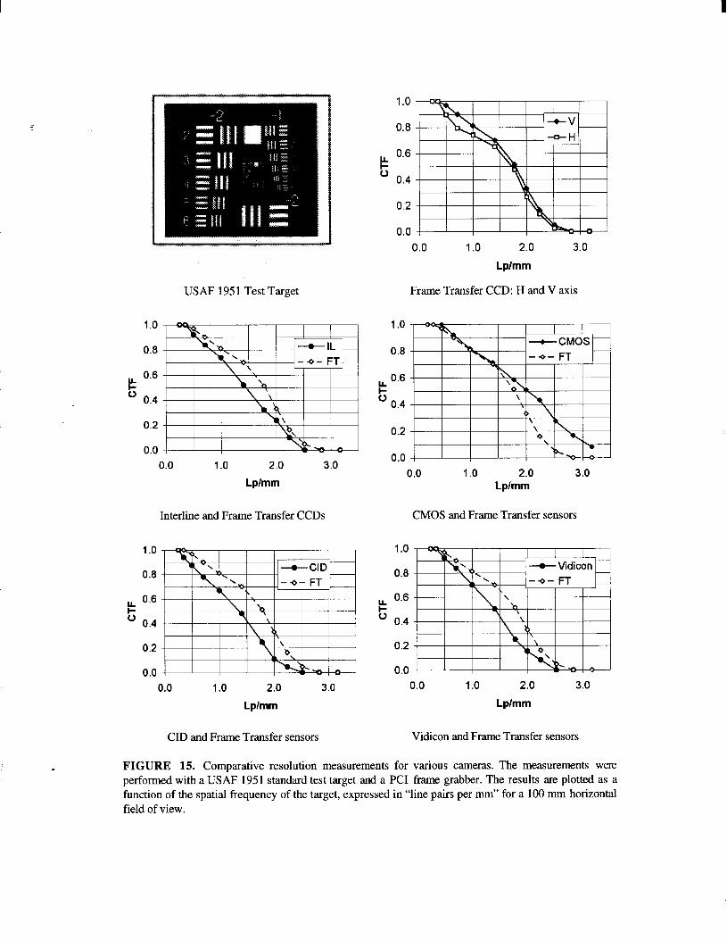
Spatial resolution measurements have been made with a standard test target [USAF 19511 and a target to sensor magnification adjusted to have always a horizontal field of view of 10 cm, typical for screen observations. The images were acquired with a PC1 frame grabber. The contrast C between the black and white bars of the test pattern in Figure 15, and the contrast transfer function (CTF), are defined as:
(1)
Cimage CTF = C testpclte
(2)
The results are summarized in Table 1 and Figure 15. The data for each camera are plotted as a function of the spatial frequency of the test plate, expressed in “line pairs per
“, together with the data of the FT CCD camera for easy comparison. The Eurements have been performed with the sensors used around SPS and LEP. They are representative of the different technologies.
The best resolution is achieved by the modem X-Y CMOS matrix. The performance improvement is enormous compared to a previous sensor tested two years ago (2). The Frame transfer CCD, now ten years old, comes second. The interline camera comes next. The performance of the Vidicon camera is good, probably better than expected by most users, slightly better than the CID camera, and makes this type of camera a good solution for radiation areas.
The performance degradation of the FT CCD camera with MCP intensifiers has to be noticed (see Table 1). This degradation will increase with repetition rate. Nevertheless, the low resistance MCP has an honorable performance and can be used when fast gating is a necessity.
TABLE 1. Spatial Resolution Measurements Normalized to the Full Sensor Size
Sensor Line pairs for 50% CTF Line pairs for 10% CTF
X-Y CMOS 200 310
CCD Frame transfer 180 240
CCD Interline 140 230
X-Y CID 140 200
V&on 140 220
Low resist. MCP [l Hz] 110 210
Normal MCP rl kHz1 40 130
USAF 1951 Test Target
k 0.6
o 0.4
0.2
0.0 j I I I I
0.0 1.0 2.0 3.0
Lplmm
Interline and Frame Transfer CCDs CMOS and Frame Transfer sensors
0.8
k 0.6
* 0.4
1.0 2.0 3.0
Lplmm
CID and Frame Transfer sensors Vidicon and Frame Transfer sensors
0.8
0.2
0.0 0.0 1.0 2.0 3.0
Lplmm
Frame Transfer CCD: H and V axis
1.0
0.8
k 0.6
o 0.4
0.0 1 .o 2.0 3.0 Lplmm
1.0
0.8
k 0.6
o 0.4
1 .o 2.0 3.0
Lplmm
FIGURE 15. Comparative resolution measurements for various cameras. The measurements were performed with a USAF 1951 standard test target and a PC1 frame grabber. The results are plotted as a function of the spatial frequency of the target, expressed in “line pairs per mm” for a 100 mm horizontal field of view.
SPECIAL FEATURES FOR BEAM INSTRUMENTATION
Beam instrumentation is a small field compared to the consumer and machine vision markets. Hence, commercially available devices are not specifically tuned toward this field and the specific demands for beam instrumentation have to be considered when choosing a system.
All of the instruments are in a radiation environment where they have to survive. The radiation dose and the lifetime to be achieved will, in general, determine the choice of sensor to be used: TV tube, CCD, CMOS, or their radiation hardened counterparts. Tubes make, of course, the most resistant cameras. At the CERN SPS such cameras are used in areas with annual doses greater thanlO Gy. Normal CCDs have shown damage at levels of 10 Gy. Radiation-hard CCDs and CIDs are claimed to resist from lo3 to 10” Gy. The radiation causes an increase in dark current resulting in an overall decrease in well capacity, i.e. in contrast, which is clearly visible on the CTF (see Figure 16). The local radiation environment will also influence the location of the processing electronics. In some accelerators, this may mean that the processing takes place hundreds of meters away from the sensor. As a consequence, frame grabber acquisitions can be degraded with respect to pure digital acquisitions. This is visible in Figure 16 with the CTF measured for the same image sensor in video mode and in digital mode. One way to overcome this limitation is maybe to use fiber optic links, as was done at RHIC (3).
1 .o
0.8
1 2 3 Lplmm
FIGURE 16. Contrast Transfer Functions. Left: for new (full diamonds) and irradiated (open figures) CCDs. Right: Digital (full diamonds) and fixme grabber (open circles) acquisitions with 1000 m of cable between sensor and digitizer.
The spectral sensitivity of the sensor has to match the available spectrum or select the best slice for the precision of the instrument. Representative spectral sensitivities are given in Figure 17. Quite a number of cameras for visual applications include infrared filters, simulating the eye sensitivity for the best use of the commercial achromats which have been optimized between 450 and 650 nm. But a popular screen material, AJO, (Cr) has a peak emission around 700 nm, at the limit of the commercial IR filters, which has given surprises in some accelerators! In general, color cameras are of little or no interest in beam instrumentation.
Back illuminated CCD
2w.l 400 600 800 1000 wmi
Screens Csl VI],, ,‘-‘-.x
8 Quartz“\, p\ AI,O, [Cr] / ii
200 4do 6;O 8dO rob0 Unml
FIGURE 17. Relative spectral sensitivities of common image sensors and spectral emission of some widely used screens.
Fast turn-by-turn beam cross-section acquisition (2), beyond the mains frequency, is useful for beam instability or beam matching observations. The latter can be performed by measuring the profile variations over several turns after injection, but before filamentation. They can be made by using the CCD chip as an analog buffer memory. The principle is explained in Figure 18. It makes use of an intensifier used as a fast shutter and a CCD used as memory, It is called the “burst mode”. The number of pulses stored on the chip can be doubled by using the full chip. The main limitation comes from the recovery time of the intensifier, limiting the acquisition frequency to around 10 kHz.
CCD image area /
1st pulse arrives
advance
\
2nd pulse 30 lines
CCD rnemoly area
9th pulse advance 30 lines
readout the - complete
memory area
FIGURE 18. Principle of the “burst mode.”
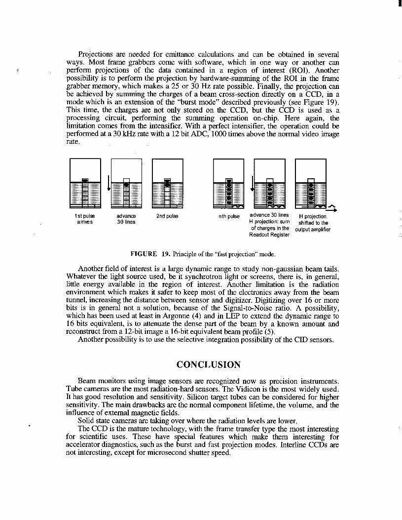
Projections are needed for emittance calculations and can be obtained in several ways. Most frame grabbers come with software, which in one way or another can perform projections of the data contained in a region of interest (ROI). Another possibility is to perform the projection by hardware-summing of the ROI in the frame grabber memory, which makes a 25 or 30 Hz rate possible. Finally, the projection can be achieved by summing the charges of a beam cross-section directly on a CCD, in a mode which is an extension of the “burst mode” described previously (see Figure 19). This time, the charges are not only stored on the CCD, but the CCD is used as a processing circuit, performing the summing operation on-chip. Here again, the limitation comes from the intensifier. With a perfect intensifier, the operation could be performed at a 30 kHz rate with a 12 bit ADC, 1000 times above the normal video image rate.
1 st pulse advance arriws 30 lines
2nd pulse nth pulse advance 30 lines H projection H projection: sum shifted to the of charges in the output amplifier
Readout Register
FIGURE 19. Principle of the “fast projection” mode.
Another field of interest is a large dynamic range to study non-gaussian beam tails. Whatever the light source used, be it synchrotron light or screens, there is, in general, little energy available in the region of interest. Another limitation is the radiation environment which makes it safer to keep most of the electronics away from the beam tunnel, increasing the distance between sensor and digitizer. Digitizing over 16 or more bits is in general not a solution, because of the Signal-to-Noise ratio. A possibility, which has been used at least in Argonne (4) and in LEP to extend the dynamic range to 16 bits equivalent, is to attenuate the dense part of the beam by a known amount and reconstruct from a 12-bit image a 16-bit equivalent beam profile (5).
Another possibility is to use the selective integration possibility of the CID sensors.
CONCLUSION
Beam monitors using image sensors are recognized now as precision instruments. Tube cameras are the most radiation-hard sensors. The Vidicon is the most widely used. It has good resolution and sensitivity. Silicon target tubes can be considered for higher sensitivity. The main drawbacks are the normal component lifetime, the volume, and the influence of external magnetic fields.
Solid state cameras are taking over where the radiation levels are lower. The CCD is the mature technology, with the frame transfer type the most interesting
for scientific uses. These have special features which make them interesting for accelerator diagnostics, such as the burst and fast projection modes. Interline CCDs are not interesting, except for microsecond shutter speed.
CMOS sensors are developing quickly. Their technology, similar to RAM, makes them cheaper to produce than CCDs, while yielding better performance than most CCDs. The machine vision and consumer market will push them to the front of the scene while pushing their prices down. Due to the on-chip processing capabilities, and considering the progress made over the past few years, it seems that they will be the image sensors of the future.
Software was not touched upon in this tutorial. A lot of it is already available commercially. Most of the frame grabbers come with sophisticated software, some of which is of direct interest in the field of beam instrumentation. Here again, it is the consumer and machine vision market which has stimulated development. It is estimated that half of the vision market, which amounts world-wide to hundreds of millions of dollars, is represented by software!
It is now possible to buy complete instruments comprised of sensor, digitizer, and software. But, because of the small market of accelerator beam instrumentation, the items available are not always adequate for these applications. Even worse, their specifications or descriptions are often misleading. One of the aims of this tutorial was to make the potential user aware of the various technologies and their performance. One must also be aware that the field is changing very rapidly.
ACKNOWLEDGMENTS
This tutorial condenses the experience accumulated over the years together with my colleagues on the optical monitors in the ISR, SPS and LEP. It is a pleasure to acknowledge their contributions, with a special mention for L. Robillard for his many sensor qualification measurements.
REFERENCES
[l] Burtin, G., et al., Proc. of the 1993 IEEE Part. Act. ConJ:, 1993, pp. 2495-2497. [2] Colchester, et al., BIW’96, AIP Con& Proc., 390, May 1996, pp. 215-222. [3] Witkover, R. L., Proc. ofthe 199.5 IEEE Part. Act. Conf., 1996, pp. 2589-2591. [4] Lumpkin, A. H., M. D. Wilke, BIW 92, AIP Con. Proc., 281, 1993,
pp. 141-149. [5] Burkhardt, H., et al., SL-MD Note 238, CERN, May 1997.