Impact of N2 Plasma Power Discharge on AlGaN/GaN HEMT Performance M.-Fatima Romero, Ana Jiménez, Fernando González-Posada Flores, Sara Martín-Horcajo, Fernando Calle and Elias Muñoz Abstract—The effects of power and time conditions of in situ N 2 plasma treatment, prior to silicon nitride (SiN) passivation, were investigated on an AlGaN/GaN high-electron mobility transistor (HEMT). These studies reveal that N 2 plasma power is a critical parameter to control the SiN/AlGaN interface quality, which di- rectly affects the 2-D electron gas density. Significant enhancement in the HEMT characteristics was observed by using a low power N 2 plasma pretreatment. In contrast, a marked gradual reduction in the maximum drain-source current density (Ins mux) an d maximum transconductance (g m max)» as well as in fy and / max , was observed as the N 2 plasma power increases (up to 40% decrease for 210 W). Different mechanisms were proposed to be dominant as a function of the discharge power range. A good cor- relation was observed between the device electrical characteristics and the surface assessment by atomic force microscopy and Kelvin force microscopy techniques. Index Terms—AlGaN/GaN high-electron mobility transistors (HEMTs), passivation, plasma treatment, silicon nitride (SiN), surface. I. INTRODUCTION G aN AND related compounds are promising semiconduc- tors for next-generation high-frequency and high-power devices, particularly at high temperature and high voltage op- eration [1], [2]. Their wideband gap allows high breakdown voltage, high saturation current, and strong radiation hardness capabilities in an AlGaN/GaN high-electron mobility transistor (HEMT), which make them potential candidates for many different applications, such as wireless communications [3], future power electronic converters [4], aerospace electronics [5], etc. Although significant progresses have been done lead- ing to record frequency performance with 300-GHz / max [6], there are still several problems to be solved concerning mainly reliability and stability [7]. One key issue is related to the surface electronic states that are strongly responsible for RF dispersion (or current collapse), preventing their widespread use and leading to low reliability [8]. Recently, it was shown that not only a suitable dielectric layer is needed to mitigate RF dispersion in AlGaN/GaN HEMTs, but the use of a plasma surface pretreatment could also play a crucial role. The most employed dielectric for this aim is silicon nitride (SiN), which is used with or without pretreatments. In that case, several pretreatments have been tried such as N 2 [9], [10], NH 3 [10], [11], O2+CF4 [12], and 0 2 + SF 6 [13]. In particular, the use of a N2 plasma pretreatment has been recently reported, although not only to mitigate RF dispersion prior to the SiN passivation layer, but also for different aims such as to reduce gate leakage current in MISHEMT devices [14], prior to ohmic contact metallization to lower contact resistance [15], or to minimize surface recovery after etching damage [16]. The different goals for using a N2 plasma pretreatment and the wide range of plasma techniques and conditions make its effects on the surface properties to be still under discussion. Some reports have shown that a nitride plasma-based surface treatment previ- ous to passivation could improve device performance, probably due to the reduction in carbon and oxides over the AlGaN surfaces [10], [17], [18]. In contrast, other authors observed that plasma produced detrimental effects in an AlGaN/GaN HEMT [13] or the formation of creation of a N 2 -deficient surface [15], suggesting that the plasma discharge conditions should play a critical role in the surface preparation. This work focuses on the in situ N2 plasma treatment prior to the SiN passivation layer, deposited by plasma-enhanced chemical vapor deposition (PE-CVD). In a previous work, we reported the beneficial effects of using a low power N 2 plasma to mitigate current collapse by reducing surface states on AlGaN/GaN HEMTs [9]. This work aims to identify how critical are the power and exposure time used during the N 2 plasma discharge that directly affect the GaN-based surface, in correlation to the AlGaN/GaN HEMT electrical charac- teristics. Therefore, it contributes to clarify the mechanisms that control the GaN-based surface properties, which are the basis for the new generation of GaN-based devices, includ- ing sensors, high-power and high-frequency HEMT devices fabrication.
Transcript
Impact of N2 Plasma Power Discharge on AlGaN/GaN HEMT Performance
M.-Fatima Romero, Ana Jiménez, Fernando González-Posada Flores, Sara Martín-Horcajo, Fernando Calle and Elias Muñoz
Abstract—The effects of power and time conditions of in situ N2
plasma treatment, prior to silicon nitride (SiN) passivation, were investigated on an AlGaN/GaN high-electron mobility transistor (HEMT). These studies reveal that N2 plasma power is a critical parameter to control the SiN/AlGaN interface quality, which directly affects the 2-D electron gas density. Significant enhancement in the HEMT characteristics was observed by using a low power N2 plasma pretreatment. In contrast, a marked gradual reduction in the maximum drain-source current density (Ins mux) a n d maximum transconductance (gm max)» as well as in fy and / m a x , was observed as the N2 plasma power increases (up to 40% decrease for 210 W). Different mechanisms were proposed to be dominant as a function of the discharge power range. A good correlation was observed between the device electrical characteristics and the surface assessment by atomic force microscopy and Kelvin force microscopy techniques.
G aN AND related compounds are promising semiconductors for next-generation high-frequency and high-power
devices, particularly at high temperature and high voltage operation [1], [2]. Their wideband gap allows high breakdown voltage, high saturation current, and strong radiation hardness capabilities in an AlGaN/GaN high-electron mobility transistor (HEMT), which make them potential candidates for many
different applications, such as wireless communications [3], future power electronic converters [4], aerospace electronics [5], etc. Although significant progresses have been done leading to record frequency performance with 300-GHz / m a x [6], there are still several problems to be solved concerning mainly reliability and stability [7]. One key issue is related to the surface electronic states that are strongly responsible for RF dispersion (or current collapse), preventing their widespread use and leading to low reliability [8]. Recently, it was shown that not only a suitable dielectric layer is needed to mitigate RF dispersion in AlGaN/GaN HEMTs, but the use of a plasma surface pretreatment could also play a crucial role. The most employed dielectric for this aim is silicon nitride (SiN), which is used with or without pretreatments. In that case, several pretreatments have been tried such as N2 [9], [10], NH3 [10], [11], O2+CF4 [12], and 0 2 + SF6 [13]. In particular, the use of a N2 plasma pretreatment has been recently reported, although not only to mitigate RF dispersion prior to the SiN passivation layer, but also for different aims such as to reduce gate leakage current in MISHEMT devices [14], prior to ohmic contact metallization to lower contact resistance [15], or to minimize surface recovery after etching damage [16]. The different goals for using a N2 plasma pretreatment and the wide range of plasma techniques and conditions make its effects on the surface properties to be still under discussion. Some reports have shown that a nitride plasma-based surface treatment previous to passivation could improve device performance, probably due to the reduction in carbon and oxides over the AlGaN surfaces [10], [17], [18]. In contrast, other authors observed that plasma produced detrimental effects in an AlGaN/GaN HEMT [13] or the formation of creation of a N2-deficient surface [15], suggesting that the plasma discharge conditions should play a critical role in the surface preparation.
This work focuses on the in situ N2 plasma treatment prior to the SiN passivation layer, deposited by plasma-enhanced chemical vapor deposition (PE-CVD). In a previous work, we reported the beneficial effects of using a low power N2
plasma to mitigate current collapse by reducing surface states on AlGaN/GaN HEMTs [9]. This work aims to identify how critical are the power and exposure time used during the N2
plasma discharge that directly affect the GaN-based surface, in correlation to the AlGaN/GaN HEMT electrical characteristics. Therefore, it contributes to clarify the mechanisms that control the GaN-based surface properties, which are the basis for the new generation of GaN-based devices, including sensors, high-power and high-frequency HEMT devices fabrication.
Fig. 1. DC IDS — VDS — VGS characteristics of the AlGaN/GaN HEMT (solid lines) passivated with SiN and the N2 plasma pretreatment at (a) 60, (b) 150, and (c) 210 W, during 1 min. Devices (open circles) passivated with SiN but without any plasma pretreatment are used as a reference. VQS = —6 to 0 V, AVQS = 1 V. LQ = 1.3 jum.
In the next section, the experimental procedure is described. In Section III, the effects of different power and time parameters during the plasma discharge are discussed in relation to electrical characterization of HEMT devices and surface analysis measurements of AlGaN/GaN heterostructures. Section IV is devoted to describe a model of the dominant mechanisms as a function of the N2 plasma power discharge. Finally, in Section V, the conclusions of this work are summarized.
II. EXPERIMENTAL PROCEDURE
Five AlGaN/GaN structure wafers provided by the same epitaxial source were used in this study. The HEMT structure consisted of (28-30) nm of Alo.2sGao.72N on 1.2 /xm of GaN grown on 4H-SÍC or sapphire substrate by metal-organic vapor phase epitaxy. A nominal carrier concentration varying from 9.3 x 10¹² to 1.1 x 1013 cm - 2 was intended. Drain and source ohmic contacts were made by alloying Ti/Al/Ti/Au. Schottky gates were fabricated by optical Pt/Ti/Au and e-beam Ni/Au lithographies, with a 1.3-/xm length and two widths of 75 and 150 /xm. The standard passivation processing consisted in a SiN layer deposition at 300 °C in a conventional RF PE-CVD system using SÍH4 and NH3 as precursors. A slightly N-rich SiN layer was obtained, with n = 1.83 and er = 7.0 as determined by ellipsometry. In this study, each wafer with HEMT devices was divided into several pieces that followed a different surface pretreatment prior to the standard passivation. After a wet cleaning with NH4OH at 50 °C, each piece was exposed to a N2 plasma discharge at 200 °C followed by the standard SiN deposition in the same reactor without breaking the vacuum. The N2 plasma power was varied from low power (60 W, where a minimum stable plasma is obtained) to medium (150 W) and high power (210 W). The N2 plasma discharge duration was increased from 1 to 20 min for the lowest power. One of the pieces was used as reference without any previous in situ cleaning or plasma pretreatment of the surface before the passivation.
The HEMT devices were characterized by dc and pulsed I—V measurements from VQS = — 6 V (1 V lower than pin-choff) to 0 V (open channel). Gate pulse period was varied from 100 ms to 1 /xs, with a constant 50% duty cycle. Moreover, gate lag measurements were performed by fixing VDS at 5.5 V and applying pulsed VQS excitation from OFF- to ON-state,
as detailed by Meneghesso et al. [19]. Besides, ¿^-parameter measurements were also carried out to evaluate JT and /m a x-
In order to analyze the N2 plasma impact on the device surface morphology and surface potential, AlGaN/GaN heterostructures and GaN (n-type) templates were analyzed by atomic force microscopy (AFM) in tapping mode and Kelvin probe force microscopy (KPFM) after each N2 plasma pretreatment. It is worth mentioning that by using KPFM, in addition to the AFM technique, the electrical effects of the N2 plasma pretreatment were possible to be analyzed even with the in situ SiN passivation film. This provides a significant advantage over other surface analysis techniques, in order to avoid uncontrollable surface oxidations or contamination after the N2 plasma treatment that may induce changes in the surface potential values [20].
III. RESULTS AND DISCUSSION
A. Electrical Characterization
The typical dc output characteristics of AlGaN/GaN HEMTs using the N2 plasma pretreatment for 1 min at 60, 150, and 210 W RF power, compared with an equivalent transistor without any plasma pretreatment, are shown in Fig. 1. Whereas a slight increase in the current and transconductance is observed after a 60-W plasma treatment, a gradual and strong reduction in IDS max and ^ m m a x , up to 33%, was measured as the N2 plasma pretreatment power increased. The drop in the current density and the positive shift in the knee voltage mean that the access resistance increases with the plasma pretreatment power, which seriously affects high-frequency device performance [21]. Electrical measurements using the transfer line method with a passivated surface reveal that the contact resistance values (Rc) hardly change with the plasma pretreatment (Rc = 0.5—0.9 Q • mm), whereas the sheet resistance (Rsheet) value rapidly increases with the N2 plasma power applied. In fact, for the high power (210 W) plasma, Rsheet values reach around 2500 O/sq, which is ^5 times higher than the case with the lower power (60 W) plasma (Rsheet = 480 fl/sq), confirming that the AlGaN surface in the active region is affected by the plasma treatment power [22]. These results highlight a strong and gradual reduction in the 2-D electron gas (2DEG) charge density in the channel and mobility as the N2 plasma power
Fig. 2. GLR versus gate pulse period (constant duty cycle of 50%, VJJS = 5.5 V) of samples (open squares) without plasma pretreatment and with N2 plasma pretreatment at (black triangles) 60, (black circles) 150, and (black squares) 210 W. Solid lines are guidelines for the eye.
increases from low (60 W) to high (250 W) plasma powers. In addition, these gradual reductions are consistent with the drop measured in the dc IDS max and the positive shift of the threshold voltage (Vth) from -4.42, to -4.07, and to -3.82 V, at 60, 150, and 210 W, respectively.
To further investigate the influence of the N2 plasma power in the trapping of charges in HEMT devices, collapse measurements were carried out. Pulsed output characteristics on AlGaN/GaN HEMTs showed similar behavior as in dc performance. IDS'max values increased for low plasma power and decreased as the plasma power was higher. In fact, devices using the lowest power plasma pretreatment (60 W) showed about 12% higher IDS max than those without any plasma pretreatment, which is in good agreement with previous results [9]. In Fig. 2, the gate lag ratio (GLR), which is defined as the ratio of the pulsed IDS value in steady state to the dc IDS value at VDS = 5.5 V, is presented for different pulse periods. For long periods, i.e., long pulse widths (around 1 ms-1 s), the GLR is almost constant for the untreated devices and for the low power N2 plasma pretreatment. Noteworthy, the GLR is almost equal to 1 (minimum current collapse) for the low power N2 plasma pretreatment and remains constant as the pulse width is narrowing. In comparison, the untreated surface device presents a worse GLR with a shorter pulse width (< 1 ms), i.e., a worse high-frequency performance. This result highlights the beneficial effects of the low power N2 plasma pretreatment to mitigate current collapse by reducing surface trap charges in the active region and improve the high-frequency performance HEMT devices [9], [10]. In contrast, in the case of higher plasma power, the GLR rapidly moves away from 1 (minimum current collapse) for pulse period narrower than 500 ms up to the shortest pulses (500 ns). This suggests that the high N2 plasma power induces trap charges generation on the AlGaN surface with charge emission time constants above 250 ns, which is consistent with Meneghesso et al. [19].
The impact of the N2 plasma power was also noticeable in RF characterization. At low plasma power, no degradation in JT and / m a x was shown, and a small (~5%) increase in / m a x
with respect to the case without a N2 plasma pretreatment was
35
30
NT 2 5 I O
o § 15
£ 10
5
HEMT with N2 plasma
- 0 - f T
¿-l_G=1.3nm -O
50 100 150 200 N2 plasma power (W)
250
Fig. 3. (Black triangles) Maximum frequency /max and (open circles) cutoff frequency JT of samples passivated with SiN and N2 plasma pretreatment at 60, 150, and 210 W, respectively. Solid lines are guidelines for the eye.
found. However, a similar 40% degradation in fr and / m a x
for the highest plasma power (210 W), with respect to the lowest power value (60 W), was observed (see Fig. 3). Since the geometry of the gate is a fixed parameter for the measured devices, the similar reduction in both JT and / m a x points out that the power plasma discharge has modified intrinsic characteristics of the heterostructure, likely by changing the surface states in the AlGaN/GaN space region between the gate and the drain/source, which is directly related to the 2DEG density. Moreover, the changes in JT and / m a x are in good agreement with the IDS max and gm m a x values and support that the mobility and charge density in the channel are affected by the plasma pretreatment.
Once established that the low (60 W) power plasma pretreatment showed the best device performance, the time exposure to the plasma was analyzed. However, not significant differences either in dc, pulsed, or RF measurements were observed for 1, 5, 10, and 20 min at the lowest RF power (60 W). These results lead to plasma duration being less critical than plasma power, and therefore, further analysis is basically focused on the effects of plasma power discharge. On the other hand, the different electrical behavior of GaN-based HEMTs as a function of plasma treatment power discharge could partially explain the dispersion from reported studies using the N2 plasma pretreatment, hence showing the importance of using a low power plasma pretreatment on GaN-based surfaces [9], [12], [16].
B. Surface Characterization
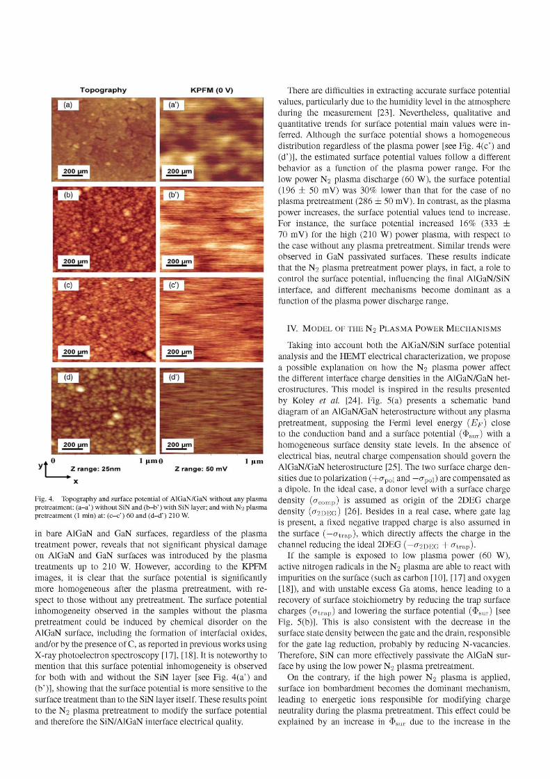
The electric characterization demonstrates that the low power N2 pretreatment makes more effective the effect of the SiN pasivation layer to mitigate collapse, whereas the use of high power plasma increases this undesirable effect. However, how does the plasma act? The topography and the corresponding surface potential are shown in Fig. 4 for different cases: first, without plasma pretreatment [for bare surface (a-a') and with the SiN layer (b-b')] and second, with N2 plasma pretreatment [at 60 W in (c-c') and at 210 W in (d-d'), both with the SiN layer]. The root-mean-square roughness obtained by AFM
Topography
1 200 pm M
KPFM (0 V)
1 200 nm ^
H^H
1 200 ym M
n^n
1 200 ym M
t__zra" ge: 25nm I ¡uiHI
Z range: 50 mV 1 ¡i m
Fig. 4. Topography and surface potential of AlGaN/GaN without any plasma pretreatment: (a-a') without SiN and (b-b') with SiN layer; and with N2 plasma pretreatment (1 min) at: (c—c') 60 and (d-d') 210 W.
in bare AlGaN and GaN surfaces, regardless of the plasma treatment power, reveals that not significant physical damage on AlGaN and GaN surfaces was introduced by the plasma treatments up to 210 W. However, according to the KPFM images, it is clear that the surface potential is significantly more homogeneous after the plasma pretreatment, with respect to those without any pretreatment. The surface potential inhomogeneity observed in the samples without the plasma pretreatment could be induced by chemical disorder on the AlGaN surface, including the formation of interfacial oxides, and/or by the presence of C, as reported in previous works using X-ray photoelectron spectroscopy [17], [18]. It is noteworthy to mention that this surface potential inhomogeneity is observed for both with and without the SiN layer [see Fig. 4(a') and (b')], showing that the surface potential is more sensitive to the surface treatment than to the SiN layer itself. These results point to the N2 plasma pretreatment to modify the surface potential and therefore the SiN/AlGaN interface electrical quality.
There are difficulties in extracting accurate surface potential values, particularly due to the humidity level in the atmosphere during the measurement [23]. Nevertheless, qualitative and quantitative trends for surface potential main values were inferred. Although the surface potential shows a homogeneous distribution regardless of the plasma power [see Fig. 4(c') and (d')], the estimated surface potential values follow a different behavior as a function of the plasma power range. For the low power N2 plasma discharge (60 W), the surface potential (196 ± 50 mV) was 30% lower than that for the case of no plasma pretreatment (286 ± 50 mV). In contrast, as the plasma power increases, the surface potential values tend to increase. For instance, the surface potential increased 16% (333 ± 70 mV) for the high (210 W) power plasma, with respect to the case without any plasma pretreatment. Similar trends were observed in GaN passivated surfaces. These results indicate that the N2 plasma pretreatment power plays, in fact, a role to control the surface potential, influencing the final AlGaN/SiN interface, and different mechanisms become dominant as a function of the plasma power discharge range.
IV. MODEL OF THE N2 PLASMA POWER MECHANISMS
Taking into account both the AlGaN/SiN surface potential analysis and the HEMT electrical characterization, we propose a possible explanation on how the N2 plasma power affect the different interface charge densities in the AlGaN/GaN het-erostructures. This model is inspired in the results presented by Koley et al. [24]. Fig. 5(a) presents a schematic band diagram of an AlGaN/GaN heterostructure without any plasma pretreatment, supposing the Fermi level energy (EF) close to the conduction band and a surface potential ($ su r) with a homogeneous surface density state levels. In the absence of electrical bias, neutral charge compensation should govern the AlGaN/GaN heterostructure [25]. The two surface charge densities due to polarization (+crpoi and —<TPOI) are compensated as a dipole. In the ideal case, a donor level with a surface charge density (<7comp) is assumed as origin of the 2DEG charge density (CT2DEG) [26]. Besides in a real case, where gate lag is present, a fixed negative trapped charge is also assumed in the surface (—otrap), which directly affects the charge in the channel reducing the ideal 2DEG (-O"2DEG + o"trap)-
If the sample is exposed to low plasma power (60 W), active nitrogen radicals in the N2 plasma are able to react with impurities on the surface (such as carbon [10], [17] and oxygen [18]), and with unstable excess Ga atoms, hence leading to a recovery of surface stoichiometry by reducing the trap surface charges (<7trap) and lowering the surface potential ($ su r) [see Fig. 5(b)]. This is also consistent with the decrease in the surface state density between the gate and the drain, responsible for the gate lag reduction, probably by reducing N-vacancies. Therefore, SiN can more effectively passivate the AlGaN surface by using the low power N2 plasma pretreatment.
On the contrary, if the high power N2 plasma is applied, surface ion bombardment becomes the dominant mechanism, leading to energetic ions responsible for modifying charge neutrality during the plasma pretreatment. This effect could be explained by an increase in $ s u r due to the increase in the
(a) w / o N2 Plasma (b) Low power plasma (c) High powe r plasma
AIGaN GaN
<D, <t>.„, - :
AIGaN
t r
i . -
;
GaN
[, Ec
E[
Ga(M
-OjDES+^trap -°ji)i(.
0|ir,
JZDEGTutí¿pJHí'
" ^ p o l " ^Irjp.HP
Fig. 5. Schematic band diagram of the AlGaN/GaN heterostructure (a) without any plasma pretreatment and after (b) low and (c) high N2 plasma power pretreatment. —(Jtrap represents the trap charges on the surface without any plasma pretreatment, and —o"trap,HP is the trap charge after the high power plasma pretreatment. <Jpoi represents the fixed polarization charges, and <JCOm is the compensating charge on the AIGaN surface.
fixed trapped negative charge density (entrap,HP) on the AIGaN surface during the high power plasma exposure [see Fig. 5(c)]. These energetic ions in a N2 discharge could produce efficient preferential loss of the nitrogen from the near-surface AIGaN region [15], which is in good agreement with the increase in trapping effects and the poor electrical characteristics shown in HEMT devices. Moreover, the increase in the surface potential with the plasma power would lead to moving the Fermi level further away from the conduction band, leading to a decrease in the ideal 2DEG charge density (-O"2DEG + o"trap,Hp), which is consistent with the electrical results.
V. CONCLUSION
The effects of power and time of the N2 plasma pretreatment used in GaN and AlGaN/GaN HEMT heterostructures and devices have been investigated. The low power (60 W) plasma treatment prior to SiN passivation was found to improve the electrical properties of surfaces, independently of the time duration up to 20 min. In contrast, the high power (150 and 210 W) plasma pretreatment showed a degradation of the electronic properties, increasing the sheet resistance of the 2DEG and increasing gate lag effects in HEMTs. Besides, a good correlation between electrical and surface characterization was shown, pointing at the N2 plasma treatment to induce different mechanisms that control the surface potential and charges as a function of the power discharge.
These results confirm that the GaN-based surface is strongly sensitive to the N2 plasma power and that the use of a low power (60 W) N2 plasma surface treatment prior to the passivation results to be a key factor in order to mitigate surface trapping effects in AlGaN/GaN HEMTs, hence helping to reduce one of the bottlenecks to improve their high-frequency performance.
ACKNOWLEDGMENT
The authors would like to thank D. López-Romero for his technical assistance and Dr. Barbet, Dr. Theron, Dr. Rius, and Dr. Pérez for the collaboration with KFM measurements.
REFERENCES
[1] F. Benkhelifa, D. Krausse, S. Mueller, R. Quay, and M. Mikulla, "AlGaN/GaN HEMTs for high voltage applications," in Proc. 5th Space Agency—MOD (ESAMOD) Round Table Workshop GaN Component Technol, Noordwijk, Netherlands, 2010.
[2] D. Maier, M. Alomari, N. Grandjean, J.-F Carlin, M.-A. Diforte-Poisson, C. Dua, A. Chuvilin, D. Troadec, C. Gaquiére, U. Kaiser, S. L. Delage, and E. Kohn, "Testing the temperature limits of GaN-based HEMT devices," IEEE Trans. Device Mater. Rel, vol. 10, no. 4, pp. 427-436, Dec. 2010.
[3] R. Vetury, Y. Wei, D. S. Green, S. R. Gibb, T. W. Mercier, K. Leverich, P. M. Garber, M. J. Poulton, and J. B. Shealy, "High power, high efficiency, AlGaN/GaN HEMT technology for wireless base station applications," in Proc. IEEE MIT-S Int. Microw. Symp., 2005, pp. 487-490.
[4] J. Everts, J. Das, J. van den Keybus, M. Germain, and J. Driesen, "GaN based power transistors for future power electronic converters," in Proc. IEEE Benelux Young Res. Symp., Leuven, Belgium, 2010.
[5] K. Son, A. Liao, G. Lung, M. Gallegos, T. Hatake, R. D. Harris, L. Z. Scheick, and W. D. Smythe, "GaN-based high temperature and radiation-hard electronics for harsh environments," Nanosci. Nanotech-nol. Lett., vol. 2, no. 4, pp. 89-95, Dec. 2010.
[6] J. W. Chung, W. E. Hoke, E. M. Chumbes, and T. Palacios, "AlGaN/GaN HEMT with 300-GHz fmax," IEEE Electron Device Lett., vol. 31, no. 3, pp. 195-197, Mar. 2010.
[7] G. Meneghesso, G. Verzellesi, F Danesin, F Rampazzo, F Zanon, A. Tazzoli, M. Meneghini, and E. Zanoni, "Reliability of GaN high electron mobility transistors: State of the art and perspectives," IEEE Trans. Device Mater. Rel, vol. 8, no. 2, pp. 332-343, Jun. 2008.
[8] I. Daumiller, D. Theron, C. Gaquiére, A. Vescan, R. Dietrich, A. Wieszt, H. Leier, R. Vetury, U. K. Mishra, I. P. Smorchkova, S. Keller, C. Nguyen, and E. Kohn, "Current instabilities in GaN-based devices," IEEE Electron Device Lett., vol. 22, no. 2, pp. 62-64, Feb. 2001.
[9] M. F Romero, A. Jiménez, J. Miguel-Sánchez, A. F Braña, F González-Posada, R. Cuerdo, F Calle, and E. Muñoz, "Effects of N2 plasma pretreatment on the SiN passivation of AlGaN/GaN HEMT," IEEE Electron Device Lett., vol. 29, no. 3, pp. 209-211, Mar. 2008.
[10] J. H. Kim, H. G. Choi, M.-W. Ha, H. J. Song, C. H. Roh, J. H. Lee, J. H. Park, and C.-K. Hahn, "Effects of nitride-based plasma pretreatment prior to SiNx passivation in AlGaN/GaN high-electron-mobility transistors on silicon substrates," Jpn. J. Appl. Phys., vol. 49, no. 4, pp. 04DF05-1-04DF05-3, Apr. 2010.
[11] A. P. Edwards, J. A. Mittereder, S. C. Binari, D. S. Katzer, D. F Storm, and J. A. Roussos, "Improved reliability of AlGaN-GaN HEMTs using an NH3 plasma treatment prior to SiN passivation," IEEE Electron Device Lett., vol. 26, no. 4, pp. 225-227, Apr. 2005.
[12] Y. Guhel, B. Boudart, N. Vellas, C. Gaquiére, E. Délos, D. Ducatteau, Z. Bougrioua, and M. Germain, "Impact of plasma pre-treatment before SiNj; passivation on AlGaN/GaN HFETs electrical traps," Solid State Electron., vol. 49, no. 10, pp. 1589-1594, Oct. 2005.
[13] D. J. Meyer, J. R. Flemish, and J. M. Redwing, "Plasma surface pretreatment effects on silicon nitride passivation of AlGaN/GaN HEMTs," in Proc. CSMANTECH Conf., May 14/15, 2007, pp. 305-307.
[14] Q. Feng, Y. Hao, and Y.-Z. Yue, "The reduction of gate leakage of AlGaN/GaN metal-insulator-semiconductor high electron mobility transistors by N2 plasma pretreatment," Semicond. Sci. Technol, vol. 24, no. 2, pp. 025 030-1-025 030-6, Feb. 2009.
[15] A. P. Zhang, G. T. Dang, F Ren, J. M. Van Hove, J. J. Klaassen, P. P. Chow, X. A. Cao, and S. J. Pearton, "Effect of N2 discharge treatment on AlGaN/GaN high electron mobility transistor ohmic contacts using inductively coupled plasma," J. Vac. Sci. Technol. A, Vac. Surf. Films, vol. 18, no. 4, pp. 1149-1152, Jul. 2000.
[16] J.-M. Lee, K.-M. Chang, S.-W. Kim, C. Huh, I.-H. Lee, and S.-J. Park, "Dry etch damage in n-type GaN and its recovery by treatment with an N2 plasma," /. Appl. Phys., vol. 87, no. 11, pp. 7667-7670, Jun. 2000.
[17] F Gonzalez-Posada, J. A. Bardwell, S. Moisa, S. Haffouz, H. Tang, A. F Brana, and E. Muñoz, "Surface cleaning and preparation in AlGaN/GaN-based HEMT processing as assessed by X-ray photoelec-tron spectroscopy," Appl. Surf. Sci, vol. 253, no. 14, pp. 6185-6190, May 2007.
[18] H. Hasegawa, T. Inagaki, T. S. Ootomo, and T. Hashizume, "Mechanisms of current collapse and gate leakage current in AlGaN/GaN het-erostructure field effect transistors," J. Vac. Sci. Technol. B, Microelectron. Process. Phenom., vol. 21, no. 4, pp. 1844-1855, Jul. 2003.
[19] G. Meneghesso, G. Verzellesi, R. Pierobon, F Rampazzo, A. Chini, U. K. Mishra, C. Canali, and E. Zanoni, "Surface-related drain current dispersion effects in AlGaN-GaN HEMTs," IEEE Trans. Electron Devices, vol. 51, no. 10, pp. 1554-1561, Oct. 2004.
[20] E. Ogawa, T. Hashizume, S. Nakazawa, T. Ueda, and T. Tanaka, "Chemical and potential bending characteristics of SiNx/AlGaN interfaces prepared by in situ metal-organic chemical vapor deposition," Jpn. J. Appl. Phys., vol. 46, no. 24, pp. L590-L592, Jun. 2007.
[21] Nidhi, T. Palacios, A. Chakraborty, S. Keller, and U. K. Mishra, "Study of impact of access resistance on high-frequency performance of AlGaN/GaN HEMTs by measurements at low temperatures," IEEE Electron Device Lett., vol. 27, no. 11, pp. 877-880, Nov. 2006.
[22] X. Z. Dang, E. T. Yua, E. J. Piner, and B. T. McDermott, "Influence of surface processing and passivation on carrier concentrations and transport properties in AlGaN/GaN heterostructures," J. Appl. Phys., vol. 90, no. 3, pp. 1357-1361, Aug. 2001.
[23] T. Xie, S. Kishimoto, and T. Mizutani, "Measurement of surface contact potencial of AlGaN/GaN heterostructure and n-GaN by Kelvin probe force microscopy," Phys. Stat. Sol. (C), vol. 0, no. 7, pp. 2372-2375, Dec. 2003.
[24] G. Koley, V. Tilak, L. F Eastman, and M. G. Spencer, "Slow transients observed in AlGaN/GaN HFETs: Effects of SiNx passivation and UV illumination," IEEE Trans. Electron Devices, vol. 51, no. 4, pp. 886-893, Apr. 2003.
[25] J. P. Ibbetson, P. T. Fini, K. D. Ness, S. P. DenBaars, J. S. Speck, and U. K. Mishra, "Polarization effects, surface states, and the source of electrons in AlGaN/GaN heterostructure field effect transistors," Appl. Phys. Lett., vol. 77, no. 2, pp. 250-252, Jul. 2000.
[26] B. Jogai, "Influence of surface states on the two-dimensional electron gas in AlGaN/GaN heterojunction field-effect transistors," J. Appl. Phys., vol. 93, no. 3, pp. 1631-1635, Feb. 2003.
É^ ^ M-Fátima Romero received the bachelor's degree
in Physics (2003) from the Complutense University of Madrid (UCM) and the PhD degree (2010) from the Polytechnic University of Madrid (UPM), Spain. Her research activity during her PhD was mainly focused on the fabrication technology and characterization of AlGaN/GaN high electron mobility transistors for wideband power amplifiers. From 2011 she has joined the department of Experimental Physics/Material Physics at Otto-von-Guericke University in Magdeburg (Germany), as Experienced Researcher within the Marie Curie European Program, where she is currently working in the optical and electrical characterization of InAlN/GaN based heterostructures for optical and electronic applications.
Ana Jiménez studied physics at the Complutense University of Madrid and Material Engineering at the Polytechnic University of Madrid, where obtained the Ph.D. degree in 2003. She has worked in MBE growth, fabrication, and characterization of AlGaN/GaN heterostructures for electronic applications. She joined University of Alcalá (Spain), department of Electrical Engineering, in January 2004 as Assistant Professor. From that her research interests are focused also on ultrasonic transducers, design of acquisition, analysis and processing sys
tems for ultrasonic transducers.
Fernando González-Posada Flores received his bachelor's degree in Physics (2003) in the Autonomic fcUniversity of Madrid and his PhD (2009) in the Telecommunication Engineering School at the Polytechnic University of Madrid, where his main research topic was the design, fabrication and characterisation of high electron mobility transistors based on Ill-nitrides. From 2010, he has joined the Nanophysics and Semiconductors group at CEA-Grenoble, where he is working in the design, fabrication and characterization of GaN nanowires
ultraviolet photodetectors.
Sara Martín-Horcajo, photograph and biography not available at the time of publication.
^^^— Fernando Calle (M'll) is graduated in Physics ^ k (1985) and PhD in Science (1990) at Universidad
Autónoma de Madrid, Spain. He has spent research stays at the Max Planck Institut FKF (Stuttgart, Germany) and Bell Labs (Murray Hill, USA).
He is researcher (1991), assistant professor (1992) and professor (2010) of Electronics at Universidad Politica de Madrid (UPM), Spain, where he contributes to the undergraduate and master programs of Electrical Engineering and Materials Engineering (Electronics, Nanotechnology, Microsystems). He
was Research Director of the Telecomm School of UPM, and Manager of the Central Facilities of the Optoelectronics Systems and Microtechnology Institute (ISOM), for which he is presently Assistant Director. His research activity is related to the physics, technology, and applications of semiconductor devices. He has experience in optical properties of III-V and II-VI heterostructures and optoelectronics applications. His current interests include wide bandgap semiconductor microelectronics for communications, harsh environments and power electronics, as well as grapheme-based devices.
Dr. Calle is author or coauthor of around 120 publications in the JCR database, has led and/or participated in 40 national and international R+D projects, and has organized several international events.
Elias Muñoz (M'80), photograph and biography not available at the time of publication.