Page 1
University of Kentucky University of Kentucky
UKnowledge UKnowledge
Theses and Dissertations--Electrical and Computer Engineering Electrical and Computer Engineering
2012
IMPROVEMENT OF SILICON OXIDE QUALITY USING HEAT IMPROVEMENT OF SILICON OXIDE QUALITY USING HEAT
TREATMENT TREATMENT
Lei Han University of Kentucky, [email protected]
Right click to open a feedback form in a new tab to let us know how this document benefits you. Right click to open a feedback form in a new tab to let us know how this document benefits you.
Recommended Citation Recommended Citation Han, Lei, "IMPROVEMENT OF SILICON OXIDE QUALITY USING HEAT TREATMENT" (2012). Theses and Dissertations--Electrical and Computer Engineering. 5. https://uknowledge.uky.edu/ece_etds/5
This Master's Thesis is brought to you for free and open access by the Electrical and Computer Engineering at UKnowledge. It has been accepted for inclusion in Theses and Dissertations--Electrical and Computer Engineering by an authorized administrator of UKnowledge. For more information, please contact [email protected] .
Page 2
STUDENT AGREEMENT: STUDENT AGREEMENT:
I represent that my thesis or dissertation and abstract are my original work. Proper attribution
has been given to all outside sources. I understand that I am solely responsible for obtaining
any needed copyright permissions. I have obtained and attached hereto needed written
permission statements(s) from the owner(s) of each third-party copyrighted matter to be
included in my work, allowing electronic distribution (if such use is not permitted by the fair use
doctrine).
I hereby grant to The University of Kentucky and its agents the non-exclusive license to archive
and make accessible my work in whole or in part in all forms of media, now or hereafter known.
I agree that the document mentioned above may be made available immediately for worldwide
access unless a preapproved embargo applies.
I retain all other ownership rights to the copyright of my work. I also retain the right to use in
future works (such as articles or books) all or part of my work. I understand that I am free to
register the copyright to my work.
REVIEW, APPROVAL AND ACCEPTANCE REVIEW, APPROVAL AND ACCEPTANCE
The document mentioned above has been reviewed and accepted by the student’s advisor, on
behalf of the advisory committee, and by the Director of Graduate Studies (DGS), on behalf of
the program; we verify that this is the final, approved version of the student’s dissertation
including all changes required by the advisory committee. The undersigned agree to abide by
the statements above.
Lei Han, Student
Dr. Zhi Chen, Major Professor
Dr. Zhi Chen, Director of Graduate Studies
Page 3
THESIS
IMPROVEMENT OF SILICON OXIDE QUALITY USING HEAT TREATMENT
A thesis submitted in partial fulfillment of the
requirements for the degree of Master of Science in Electrical Engineering
in the College of Engineering
at the University of Kentucky
Lei Han
Lexington, Kentucky
Directors: Dr. Zhi Chen, Professor of Electrical Engineering Department
Lexington, Kentucky
2012
Copyright © Lei Han 2012
By
Page 4
In decades, the tremendous development of integrated circuits industry could be mostly
attributed to SiO2, since its satisfactory properties as a gate dielectric candidate. The
effectivity of SiO2 has been challenged since dielectric layer was scaled down below
3nm, when the gate leakage current of SiO2 became unacceptable. Institution to silicon-
based CMOS techniques were proposed, but they have their own limitations. Nowadays,
materials with high dielectric constants are mainstream gate dielectric materials in
industry, but a SiO2 interfacial layer is still necessary to avoid gap between gate dielectric
layer and Si substrate, and to minimize interface trap charges. In this thesis work, by ap-
plying lateral heating process on Si wafer with thermally grown ultrathin SiO2, the gate
leakage current density could be reduced by 3-5 order of magnitude. MOS capacitors
were fabricated, and electrical properties were tested with semiconductor parameter ana-
lyzer and LCR meter. The underlying mechanism of this appealing phenomenon was ex-
plored. Since unacceptable gate leakage current is one of the main reasons which prevent
the scaling trend in semiconductor industry, this technology brings a possibility to post-
pone the end of scaling trend, and pave a way for extensive application in industry.
A new method for fabrication of MOS capacitors metal gate has been developed, and
lift-off process has been replaced by wet etching process. This method provides better
contact between dielectric layer and metal gate, meanwhile much easier operation.
KEYWORDS: Gate Leakage Current, Silicon Oxide, Leatral Heating Process, Silicon
Structure Change, Wet Etching
ABSTRACT OF THESIS
IMPROVEMENT OF SILICON OXIDE QUALITY USING HEAT TREATMENT
Lei Han
June 2, 2012
Page 5
IMPROVEMENT OF SILICON OXIDE QUALITY USING HEAT TREATMENT
By
Lei Han
Director of Thesis
Director of Graduate Studies
Dr. Zhi Chen
Dr. Zhi Chen
June 2, 2012
Page 6
iii
ACKNOWLEDGMENTS
I would like to thank my academic advisor, Dr Zhi David Chen, for the opportunity he
gave me to pursue my degree in the filed of semiconductor devices, and all the guidance
and help I’ve received from him all through these years. This thesis would be impossible
without his extensive knowledge and innovative ideas in this field.
Special thanks should be accorded to Dr Chuck May and Brian Wajdyk for providing
technical assistance at the Center for Nanoscale Science and Technology at University of
Kentucky, and for helping me solving technical problems in my fabrication process.
I would also like to thank Dr. Todd Hastings, Dr. Vijay Singh, and Dr. Fuqian Yang,
for serving as committee members, and for the insightful guidance I’ve received from
them.
Thanks to my labmate, Yichun Wang, for the time and effort she spent on my fabrica-
tion training process. I would also like to thank all my group members, Dr. Youngsik
Song, Dr. Chi Lu, Dr. Shibin Li, Dr. Ibrahim Yucedag, Jun Fang, Chenglin Yi, Mengmei
Liu, Bojie Chen, Riasad Badhan.
Last but not least, I would like to express my deepest gratitude to my parents, for the
endless love and support I have always been with since I was born.
Page 7
iv
TABLE OF CONTENTS
ACKNOWLEDGMENTS ................................................................................................. iii
LIST OF TABLES ...............................................................................................................v
LIST OF FIGURES ........................................................................................................... vi
Chapter 1 Introduction .........................................................................................................1
1.1 History of Device Scaling in Integrated Circuits .......................................................1
1.2 The Benefits of Device Scaling .................................................................................3
1.3 Scaling of the Gate Dielectrics ...................................................................................5
1.4 Moore’s Law Is Approaching an Limitation ..............................................................7
1.5 The Novel Phenomenon of Gate Dielectric Leakage Current Reduction ..................9
1.5.1 Theoretical background: Hydrogen/Deuterium isotope effect ..........................9 1.5.2 Phonon energy coupling enhancement effect ..................................................11
1.6 Motivation ................................................................................................................13
Chapter 2 MOS Capacitors Fabrication .............................................................................18
2.1 RCA Clean ...............................................................................................................18
2.2 Thermal Growth of Silicon Oxide ...........................................................................19
2.3 Introduction and Improvement of Heat Treatment Equipment ................................21
2.4 Lift-off Process for Patterning of MOS Capacitors Gates .......................................22
2.5 Back-side contact and post metallization annealing ................................................24
2.6 Current-Voltage, Capacitance-Voltage characteristics measurement ......................24
Chapter 3 Wet Etch Process for Patterning of MOS Capacitors Gates .............................28
Chapter 4 Rapid Thermal Process with Moisture ..............................................................39
Chapter 5 Lateral Heating Process Experiments and Results ............................................44
5.1 Background ..............................................................................................................44
5.2 Effect of Direct Hanging and Heat Transportation ..................................................45
5.3 Effect of Sandwich Structure ...................................................................................53
Chapter 6 Conclusion and Future Work ............................................................................59
6.1 Conclusion ...............................................................................................................59
6.2 Future Work .............................................................................................................59
Reference... ........................................................................................................................61
Vita……............... ..............................................................................................................65
Page 8
v
LIST OF TABLES
Table 1.1: Performance parameters improvement by constant-field scaling, α is the
scaling factor for dimensions[9][10]
. ....................................................................5
Table 3.1: Thin and thick silicon oxide thickness before and after 6 minutes etching. The
etchant is composed by 150ml DI water and 1g FeCl3. Point 1 and 2 represent
different locations on the same sample. The spectroscopic ellipsometry
measurement error is less than 0.05Å. .............................................................31
Page 9
vi
LIST OF FIGURES
Figure 1.1. Plot of CPU transistor counts against dates of introduction. Note the
logarithmic scale; the fitted line corresponds to exponential growth, with
transistor count doubling every two years. ......................................................15
Figure 1.2. Direct tunneling band diagram for ultra thin SiO2 ..........................................16
Figure 1.3. FTIR spectroscopy of the phonon energy coupling enhancement (PECE)
effect between the Si-O rocking mode and the Si-Si TO phonon mode before
and after RTP and deuterium annealing. Tox=230Å. RTP is carried out in N2
at 1050C for 4 minutes, deuterium anneal is carried out in N2:D2=10:1at
450C for 30 minutes after back side metallization[38]
. ...................................17
Figure 2.1. Improved RTP gas system. O2 analyzer and dew point sensor are applied to
control the O2 concentration and the humidity. ...............................................25
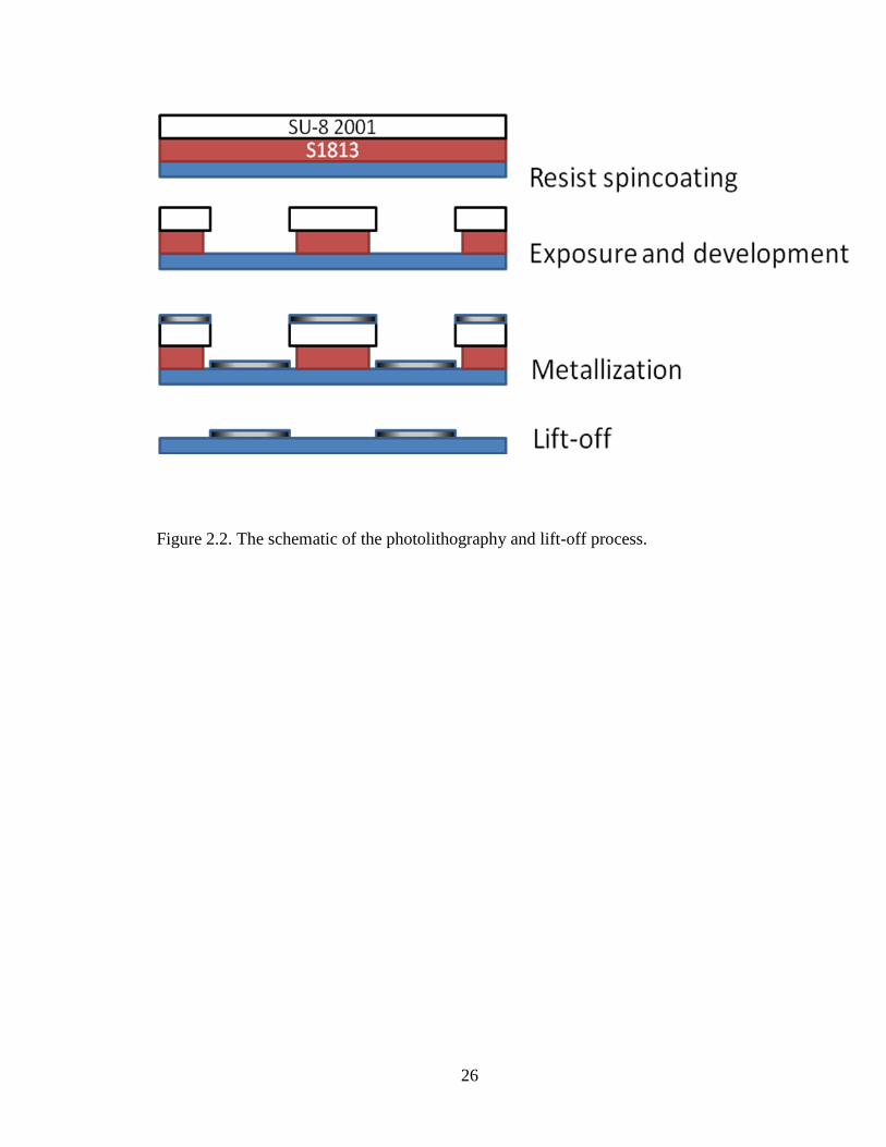
Figure 2.2. The schematic of the photolithography and lift-off process. ...........................26
Figure 2.3. The SEM image of the bilayer resist undercut structure. ................................27
Figure 3.1. Undercut of Ni pattern after FeCl3 etching. Photoresist was hard baked after
photolithography. .............................................................................................33
Figure 3.2. Undercut of Ni pattern after FeCl3 etching. Photoresist was not hard baked
after photolithography. .....................................................................................34
Figure 3.3. Severe damaged Ni gate by undercut in FeCl3 solution etching process. .......35
Figure 3.4. Peel off of Ni sheets after diluted FeCl3 solution etching and ultrasonic. .......36
Figure 3.5. MOS capacitors gates achieved by wet etching process. ................................37
Figure 3.6. The schematic of the wet etch process. Etchant 1: 100ml DI water with 40ml
HCl. Etchant 2: 150ml DI water with 1g FeCl3. ..............................................38
Figure 4.1. Gas route to test moisture effect on heat treatment. ........................................41
Figure 4.2. Capacitance density-voltage characteristics of n-type MOS capacitors before
and after rapid thermal process with moisture exists, flatband voltages and
EOTs extracted from the characteristics are marked. ......................................42
Figure 4.3. Current density-voltage characteristics of n-type MOS capacitors before and
after rapid thermal process with moisture exists. .............................................43
Figure 5.1. Special condition when obvious gate leakage current reduction could be
available. After several times’ RTP, the 4’’ Si substrate became convex, and
the good results are available in the sample’s hanging edges. .........................44
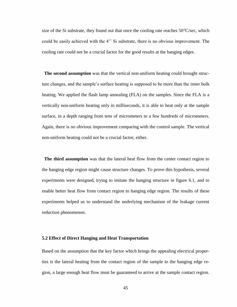
Figure 5.2. The schematic of Si step structure etching by TMAH. ...................................49
Page 10
vii
Figure 5.3. Modification of the existing Modular Process Technology Corp. model RTP-
600S system. Direct hanging and large lateral heat flow could be easily
achieved with this structure. ............................................................................50
Figure 5.4. Capacitance density-voltage characteristics of n-type MOS capacitors before
and after lateral heating process with a substrate step structure, flatband
voltages and EOTs extracted from the characteristics are marked. .................51
Figure 5.5. Current density-voltage characteristics of n-type MOS capacitors before and
after lateral heating process with a substrate step structure, gate leakage
current densities at V=VFB+1 are marked. .......................................................52
Figure 5.6. The top view (above) and the side view (bottom) of the RTP sandwich
structure. MOS capacitors gate leakage current great reduction is observed in
the hanging edge region. ..................................................................................56
Figure 5.7. Capacitance density-voltage characteristics of the n-type MOS capacitors
before and after lateral heating process, flatband voltages and EOTs extracted
from the characteristics are marked. ................................................................57
Figure 5.8. Current density-voltage characteristics of the same MOS capacitors. There is
4 to5-order-of-magnitude gate leakage current reduction after the lateral
heating process. ................................................................................................58
Page 11
1
Chapter 1 Introduction
1.1 History of Device Scaling in Integrated Circuits
Before the invention of semiconductor devices, vacuum tubes and relays were the
dominant circuit functional devices. In the summer of 1945, Kelly, the president of Bell
Laboratories at that time, built a research group. The purpose of that research group was
to explore semiconductor materials, and create solid-state devices. These devices had the
potential of replacing vacuum tubes and relays in circuits[1]
. This is the beginning of the
development of semiconductor devices, and the effect of semiconductor devices has
influenced every aspect of human’s life during the past decades until nowadays. Five
years after the establishment of Kelly’s group, in 1950, transistor was invented[2]
, which
is mainly attributed to W. Shockley, J. Bardeen, and W. Brattain. In 1960s, the metal-
oxide-semiconductor field-effect-transistor (MOSFET) was invented, followed by a
flourishing integrated circuit era[3]
. The complementary metal-oxide-semiconductor
(CMOS) technology has provided a basic element for very-large-scaled integrated circuit
(VLSI), without which the modern computer science essential to almost every aspect of
the society would be impossible.
Originally in 1965[4]
, G. E. Moore, co-founder of Intel Corporation, brought up the
Moore’s Law for the first time, which later became one of the basic principles in
integrated circuits industry. 10 years later, the Moore’s Law was modified into the most
well-known statement[5]
: the number of transistors that can be placed inexpensively on an
integrated circuit will be doubled approximately every two years. This principle is clearly
shown in Figure 1.1[6]
. During the past decades, the Moore’s Law has always been
Page 12
2
successful in elucidating and predicting the integrated circuits industry development path.
One of the key parameters that is applied to illustrate the semiconductor manufacture
processes is the average half-pitch (i.e., half the distance between identical features in an
array) of a memory cell. The International Technology Roadmap for Semiconductors
(ITRS) named these technology nodes and used them as the milestones in the
semiconductor manufacture developing trend, which are summaried as follow: 10 µm
process in around 1971; 3 µm process in around 1975; 1.5 µm process in around 1982; 1
µm process in around 1985; 800 nm process in around 1989; 600 nm process in around
1994; 350 nm process in around 1995; 250 nm process in around 1998; 180 nm process
in around 1999; 130 nm process in around 2000; 90 nm process in around 2002; 65 nm
process in around 2006; 45 nm process in around 2008; 32 nm process in around 2010.
The ITRS also predicted the 22 nm process approximately in 2011, 16 nm process
approximately in 2013, and 11 nm process approximately in 2015[7]
.
The success of integrated circuits industry with early work could be largely attributed to
the success of silicon dioxide (SiO2) as the gate dielectric for MOSFET. The properties
that make SiO2 an outstanding candidate for gate dielectric include high resistivity,
excellent dielectric strength, high melting point, a large band gap and low defect density
at the Si/SiO2 interface. Furthermore, SiO2 could be easily grown on Si substrate at a low
cost, which explains why Si has dominated the semiconductor industry for decades
among other semiconductor materials such as Ge, GaAs, InP etc.
Page 13
3
1.2 The Benefits of Device Scaling
One of the amazing things about the development of semiconductor devices is that, the
MOSFET design today is not fundamentally different from the MOSFET design decades
before, the performance improvement during the period is mainly brought about by
“scaling”, which was discovered in 1972 by Bob Dennard of IBM[8]
. Simply speaking,
scaling means the active dimensions of the integrated circuits components have being
keeping decreasing. It is mainly the scaling process that provides the performance gain of
30% per generation.
The most obvious benefit of continuous scaling is higher packing density. As the MOS
components becoming smaller, less chip area is needed for the same number of
components, or more components could be integrated into the same chip area. The
electronic products could then become smaller, more portable with various functions. A
good example for this point is the increasing laptop memory. Additionally, in modern
semiconductor technology, electronic devices on chips are fabricated using integrated
methods, more components on the same chip means higher production efficiency.
Scaling reduces the RC delay of MOSFETs, providing faster devices with higher
operation frequency. The main physical dimensions of transistors scaled are the channel
length, channel width, and the gate oxide thickness. In this way, the transistor channel
resistance, which is defined as
ALR (1.1)
(ρ is the material’s resistivity, L is the channel length, A is the channel cross area), would
Page 14
4
remain unchanged, while gate capacitance, which is defined as
At
Cox
sox
0 (1.2)
(ε0 is the vacuum dielectric constant (8.85×10⁻¹⁴
F/cm), εs is the relative dielectric con-
stant (3.9 for SiO2), tox is the gate oxide physical thickness, and A is the area of the gate
capacitor), would be cut by the scaling factor α. The time constant of a RC circuit is de-
fined as τ=R×C, hence, the RC delay of the MOSFETs scales with the same scaling fac-
tor α. The operation frequency increases as the circuit delay decreases, as a result, the op-
eration frequency becomes α times of the original value.
The Isat of MOSFETs increases with the MOSFET scaling, which is a desirable property
in high performance MOSFETs. Isat is the source-drain current of MOSFETs when
working in saturation region, that is the “on” mode of MOSFETs, and it acts as the
driving current for the follow-up circuits. Thus, higher ID,sat enables higher speed of the
whole integrated circuits. ID,sat could be written as[9]
:
2
2
,TG
oxsatD
VVC
L
WI
(1.3)
where W and L are the width and length of the MOSFET channel, respectively, μ is the
charge carrier effective mobility, Cox is the gate oxide dielectric capacitance density
(ox
s
oxt
C 0 ), VG and VT are gate voltage and threshold voltage, respectively. While W
and L are scaled by the same scaling factor α, resulting no effect on satDI , , the scaled tox
would result higher Cox, bringing higher satDI , .
Page 15
5
1.3 Scaling of the Gate Dielectrics
Many kinds of scaling concepts and technologeis exist, one of them is named “constant-
field scaling”. This concept proposes a scaling factor α, all of the MOSFET physical
dimensions are reduced by α, the body doping concentration is increased by α, and the
voltage is also reduced by the same α. In this situation, the depletion region of the
MOSFETs would be scaled with the same ratio. The basic working principle is that if a
constant electric field is maintained while shrinking a MOSFET, all other performance
parameters would be improved, which is illustrated in table 1.1[10][11]
.
Table 1.1: Performance parameters improvement by constant-field scaling, α is the scal-
ing factor for dimensions[10][11]
.
Parameter Constant-field scaling
Physical dimensions 1/α
Body doping concentration α
Voltage 1/ α
Circuit density 1/ α2
Capacitance per circuit 1/ α
Circuit speed α
Circuit power 1/ α2
Power density 1
Power-delay product 1/ α3
Based on the principle demonstrated above, all of the MOSFET physical dimensions
Page 16
6
should be scaled together. Plus, in order to maintain a good control of short-channel
effect, the gate oxide thickness of MOSFETs should be scaled nearly in proportion to the
channel length[5]
. For decades, the Intel gate oxides have been following the principle:
tox=L/45[12]
. In a long period, the continuous scaling of SiO2 had been successful until the
channel length L reached 7nm, and the physical thickness of gate oxides reached under
2nm, when the gate leakage current became unacceptable[13]
. For SiO2 gate dielectric
thinner than 3 nm, the gate leakage current mechanism is mainly quantum-mechanical
tunneling, especially direct tunneling[14]
. The direct tunneling band diagram is shown in
Figure 1.2[15]
. It has also been reported that, in this physical thickness region, the gate
leakage current magnitude will be increased by an order for each 0.2 nm decrease of the
gate dielectric thickness[16]
.
Based on the analysis above, a inference was made that in order to keep continuous
improvement of the MOSFETs’ performance, a material which is physically thick, that
could be able to keep electrons from tunneling through, and electrically thin, that could
be able to match the channel length scaling, was desirable. Dielectric materials with high
dielectric constants (high-k) was applied to meet all the requirements, and they are
becoming the dominant dielectric materials in semiconductor field. The electrical
thickness of the high-k materials is decided by the “Equivalent Oxide Thickness” (EOT),
which indicates how thick a SiO2 film should be to produce the same effect as the high-k
material film.
k
k
oxide tEOT
(1.4)
where εoxide is the relative dielectric constant of SiO2 (3.9), εk is the relative dielectric
Page 17
7
constant of the high-k gate dielectric material, and tk is the physical thickness of the high-
k gate dielectric material. A variety of materials exist with higher k value than SiO2,
ranging from Si3N4 with a k value of 7, to Pb-La-Ti (PLT) with a k value of 1,400.
However, a high-k dielectric material being able to substitute SiO2 should meet certain
requirements, in a systematc consideration include permittivity, band gap, band
alignment to silicon, thermodynamic stability, film morphology, interface quality,
compatibility with the materials used in CMOS devices processing, process compatiblity,
and reliability[17]
.
The up-to-date channel length scaling beyond the 22 nm node requires gate dielectrics
EOT < 6 Å to suppress short-channel effects[18]
. Highly scaled high-k based gate
dielectrics with EOTs of 5-6 Å in nMOSFET devices have been reported[18][19]
. Recently,
a record-setting Hf-based high-k gate dielectrics with EOT of 4.2 Å has been achieved
with a “remote interfacial layer scavenging process”[20]
.
1.4 Moore’s Law Is Approaching an Limitation
Questions about the end of scaling have always existed during the scaling process,
although all the limitation predictions raised before have been proved to be failures. One
of such predictions was the “lithography barrier,” which predicted that since
photolithography process was applied in fabrication, people cannot make spatial
resolution smaller than the light wavelength (157 nm for a KrCl Excimer laser) [11][21][22]
.
Another such predictions was the “oxide scaling barrier,” which claimed that since the
gate leakage current becomes unacceptable when the gate oxide thickness is below 3 nm,
Page 18
8
this is the final barrier for scaling[11][23][24]
.
However, the continuous scaling process cannot last forever, an ultimate limitation will
come sooner or later. MOSFETs can only be effective when they can maintain switch
functions[25]
, which means MOSFETs should be able to provide a suffcient drive current
during the “on” state, and a low enough leakage current during the “off” state.
Satisfactory drive current is available with MOSFETs’ scaling as illustrated before, the
main challenge is to maintain low “off” state leakage current, which is mainly consisted
of thermionic emission above the channel potential barrier, band-to-band tunneling
between the body and drain p-n junction, and quantum mechanical tunneling directly
between the source and drain[25]
. Additionally, the gate dielectrics EOT has already been
scaled down to a few angstroms, which is just several atomic layers. In 2003, Intel
claimed that the transistors cannot be scaled below the size achievable at 16 nm process
(5 nm gate dielectrics) due to quantum tunneling, regardless of the materials used, and the
scaling deadline is predicted to lay in between 2013 and 2018[26]
. On April 13rd, 2005, G.
E. Moore also stated in an interview himself that the Moore’s Law cannot be sustained
indefinitely.
In order to prolong the electronic components scaling limitation which is already above
the horizon, innovative materials, techniques and device ideas are continuously desirable,
among which an institution to silicon-based CMOS technique is attracting more and more
research enthusiasm. The non-silicon extension of CMOS, such as III-V materials[27]
and
nanotubes/nanowires based devices[28][29]
, as well as non-CMOS platforms, such as
Page 19
9
molecular electronics[30]
, spin-based computing[31]
, and single-electron devices[32]
, have
been proposed. However, those exotic materials and devices have their own limitations,
especially when they are aimed for large scale manufacturing. Therefore, exploring novel
phenomena for improvement of silicon based MOS devices is still very important.
1.5 The Novel Phenomenon of Gate Dielectric Leakage Current Reduction
1.5.1 Theoretical background: Hydrogen/Deuterium isotope effect
Due to high electric field in the scaling MOSFETs’ channel, some carriers in the channel
are ionized, which obtain larger energy level than the thermal energy in equilibrium.
These carriers are termed as hot carries, and they could achieve an exceedingly high
velocity. Even though these hot carriers could increase the speed of MOSFETs, they
could also have adverse effects on the reliability of devices, especially on the increasing
of Si dangling bonds at the Si/SiO2 interface. The Si dangling bonds are referred to as
interfacial traps, and they degrade the performance of MOSFETs. Post metallization
annealing in hydrogen ambient is carried out to passivate the Si dangling bonds, but the
resulting Si-H bonds are not stable, which could be easily broken by energetic hot
carriers in the channel.
Lyding et al. compared the passivation of the Si dangling bonds with both hydrogen and
deuterium[33]
, and it is proved that the Si-D bonds are more resistive to hot electron deg-
radation than Si-H bonds. This is the hydrogen/deuterium isotope effect: Si-D bonds are
Page 20
10
much stronger than Si-H bonds. By applying deuterium annealing, the hot electron deg-
radation could be improved by ~50 times[33][34][35]
.
Van de Walle et al. explained the hydrogen/deuterium isotope effect with two compet-
ing processes[36]
: (1) the vibrational energy of bonds is accumulated through multiple vi-
brational excitation by energetic hot electrons in the low voltage regime. The energy of
the bonds is increased to a point where the bonds are broken; (2) an opposite de-
excitation process exists, where the vibrational energy of the Si-D bonds are reduced by
energy coupling to the Si-Si TO phonon mode in the substrate. While there is almost no
coupling between the Si-H bending mode (650 cm-1
) and the Si-Si TO phonon mode (463
cm-1
), there is strong coupling between the Si-D bending mode (460 cm-1
) and the Si-Si
TO phonon mode. The de-excitation process is much more efficient with the Si-D bonds
than the Si-H bonds, which leads to the conclusion that the Si-D bonds are more robust to
hot electron degradation than the Si-H bonds.
Page 21
11
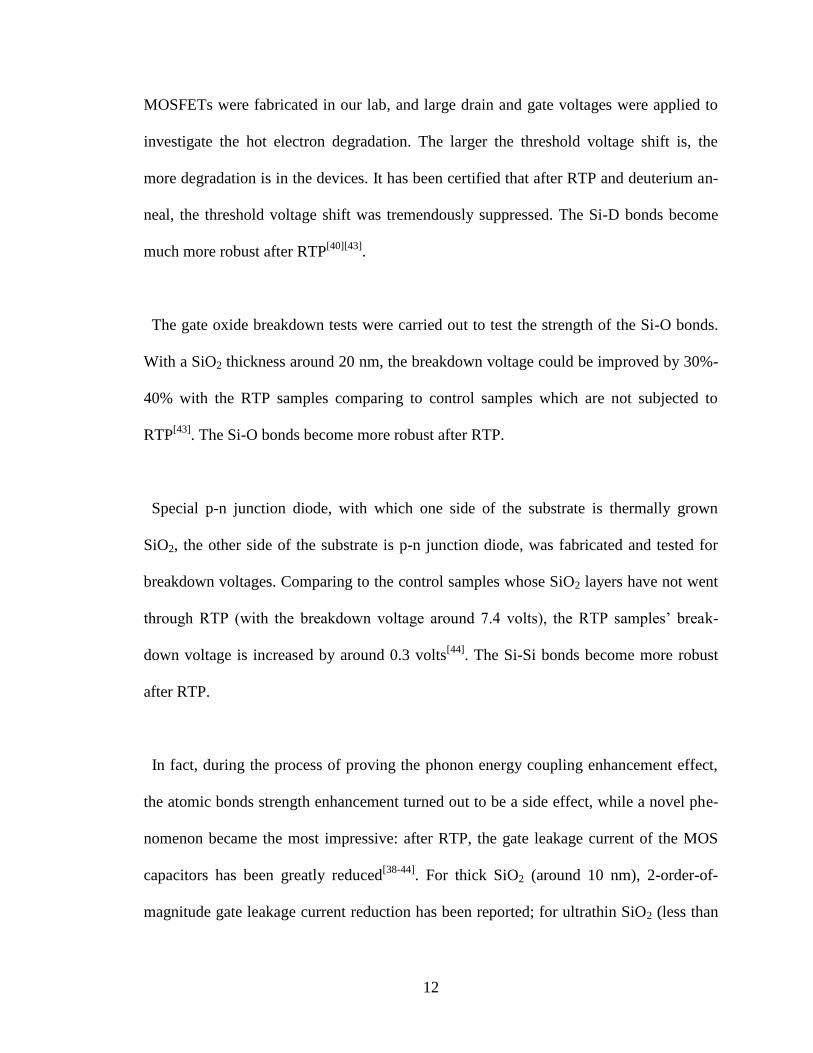
1.5.2 Phonon energy coupling enhancement effect
Certain mismatch has been reported between the Si-D vibrational mode and the Si-Si TO
phonon mode[37]
, and it was also observed in the previous work of our lab[38]
. Dr. Zhi Da-
vid Chen, professor in Department of Electrical and Computer Engineering, University of
Kentucky, made the assumption that in the Si/SiO2 system, if the Si-D vibrational mode
could be shifted toward the Si-Si TO phonon mode, the hydrogen/deuterium isotope ef-
fect might be tremendously enhanced. Rapid Thermal Process (RTP) was used to supply
thermal stress, which is supposed to introduce the atomic bonds vibrational modes shift.
By applying the RTP directly on thermally grown SiO2, phonon energy coupling en-
hancement effect was found by Dr. Chen and his students[39][40][41][42][43]
. Fourier-
Transform-Infrared (FTIR) spectroscopy is applied to prove the assumption, which is
shown in figure 1.3, along with the process parameters of RTP and deuterium anneal.
While there is no obvious shift of the Si-D vibrational mode and the Si-Si TO phonon
mode, which means the coupling between these two modes have not been strengthed,
there is large increase in the FTIR absorption intensity after RTP, the absorbance of the
Si-Si TO phonon mode and the Si-O TO rocking mode are tremendously enhanced. The
phonon energy coupling enhancement happens between the Si-Si TO phonon mode and
the Si-O TO rocking mode, and the Si-Si TO phonon mode intensity is increased by
about 50% after RTP[38]
.
The electrical characteristics of devices are also achieved, which provide more experi-
mental evidences for the phonon energy coupling enhancement effect. Large size
Page 22
12
MOSFETs were fabricated in our lab, and large drain and gate voltages were applied to
investigate the hot electron degradation. The larger the threshold voltage shift is, the
more degradation is in the devices. It has been certified that after RTP and deuterium an-
neal, the threshold voltage shift was tremendously suppressed. The Si-D bonds become
much more robust after RTP[40][43]
.
The gate oxide breakdown tests were carried out to test the strength of the Si-O bonds.
With a SiO2 thickness around 20 nm, the breakdown voltage could be improved by 30%-
40% with the RTP samples comparing to control samples which are not subjected to
RTP[43]
. The Si-O bonds become more robust after RTP.
Special p-n junction diode, with which one side of the substrate is thermally grown
SiO2, the other side of the substrate is p-n junction diode, was fabricated and tested for
breakdown voltages. Comparing to the control samples whose SiO2 layers have not went
through RTP (with the breakdown voltage around 7.4 volts), the RTP samples’ break-
down voltage is increased by around 0.3 volts[44]
. The Si-Si bonds become more robust
after RTP.
In fact, during the process of proving the phonon energy coupling enhancement effect,
the atomic bonds strength enhancement turned out to be a side effect, while a novel phe-
nomenon became the most impressive: after RTP, the gate leakage current of the MOS
capacitors has been greatly reduced[38-44]
. For thick SiO2 (around 10 nm), 2-order-of-
magnitude gate leakage current reduction has been reported; for ultrathin SiO2 (less than
Page 23
13
3.5 nm), 3 to 5-order-of-magnitude gate leakage current reduction has been reported.
1.6 Motivation
Although materials with high dielectric constant are the mainstream dielectric materials
in semiconductor industry nowadays, silicon oxide is still unavoidable. Direct deposition
of high-k dielectric layer cannot avoid gaps between dielectric layer and semiconductor
substrate, and the trap charges exist in the interface, even atomic layer deposition (ALD)
is applied[45]
. In order to get gate dielectric layer with high quality, the native oxide layer
on the Si substrate must be removed; governed by the working principle of ALD, H-
terminated Si (H/Si) substrate is necessary for thin film growth. Both of these purposes
could be easily achieved by RCA cleaning and hydrofluoric acid (HF) etches. However,
the H-terminated Si substrate is thoroughly hydrophobic, which results a large barrier to
HfO2 nucleation process. The ALD growth with this nucleation barrier is characterized
by nonlinear growth rate and discontinuous interior structure, which serves as electric
leakage path. Thus, a SiOx interfacial layer with satisfactory properties is desired.
The underlying mechanism of the phenomenon, impressive gate leakage current reduc-
tion, is still not clear. Is it because of phonon energy coupling enhancement (PECE), or
some unknown material structure changes? The conditions which cause the gate leakage
current reduction are crucial. Without clear understanding, it is very difficult to produce
the gate leakage current reduction effect reproducibly. Because this effect can reduce the
tunneling current of gate oxide, it is of great interest to use this effect to reduce the leak-
age current of high-k gate oxide stacks, which may further improve the properties of the
Page 24
14
silicon MOS devices, and pave a way for extensive applications of this technology in in-
dustry.
Page 25
15
Figure 1.1. Plot of CPU transistor counts against dates of introduction. Note the logarith-
mic scale; the fitted line corresponds to exponential growth, with transistor count dou-
bling every two years[6]
.
Page 26
16
Figure 1.2. Direct tunneling band diagram for ultra thin SiO2[14]
.
Page 27
17
Figure 1.3. FTIR spectroscopy of the phonon energy coupling enhancement (PECE) ef-
fect between the Si-O rocking mode and the Si-Si TO phonon mode before and after RTP
and deuterium annealing. Tox=230Å. RTP is carried out in N2 at 1050C for 4 minutes,
deuterium anneal is carried out in N2:D2=10:1at 450C for 30 minutes after back side
metallization[38]
.
Page 28
18
Chapter 2 MOS Capacitors Fabrication
In order to characterize silicon oxide material properties after heat treatment, simple
MOS capacitors with SiO2 as gate dielectric layer are fabricated, and current-voltage (I-
V), capacitance-voltage (C-V) curves are tested. Key parameters which reflect properties
of MOS capacitors, such as flatband voltage (VFB) and equivalent-oxide-thickness (EOT),
could be extracted from the curves.
2.1 RCA Clean
RCA cleaning is a standard set of silicon wafer cleaning steps in semiconductor manufac-
turing which needs to be performed before any crucial steps, especially high temperature
processing steps.
RCA cleaning was firstly developed by Werner Kern in 1965, while he was working for
RCA, the Radio Corporation of America[46]
. The purposes of the RCA cleaning, listed
according to the cleaning steps, are to remove organic contaminants (such as dust parti-
cles, grease or silica gel) from the wafer surface; then remove any oxide layer that may
have built up during the prior steps; finally remove any ionic or heavy metal contami-
nants[47]
.
The RCA cleaning procedures are listed below:
Step 1: Removal of grease, etc.
(1) Acetone cleaning with ultrasonic machine, 3 minutes.
(2) Isopropyl alcohol cleaning with ultrasonic machine, 3 minutes
Page 29
19
(3) Thoroughly rinse with DI water (deionized water).
Step 2: Removal of native oxide.
(1) Immerse in a (20:1) solution of DI water: HF for 30 seconds.
Check the sample surface is hydrophobic or hydrophilic after this step. Bare Si
surface should be hydrophobic. If the surface is still hydrophilic, there is still SiO2
residual, the sample needs to be etched for longer time.
(2) Thoroughly rinse with running DI water in 30 seconds.
This step should be finished in 30 seconds, otherwise Si oxide layer will grow
agian.
Step 3: RCA 1 (or SC 1), removal of organic (dust particles, grease or silica gel) / metal
ionic (Cu, Ag, etc.) contamination.
(1) Immerse in a (5:1:1) solution of DI water: NH4OH: H2O2 at 75-80°C for 10
minutes.
(2) Thoroughly rinse with DI water.
Step 4: Removal of chemical oxide formed during RCA 1.
(1) Immerse in a (20:1) solution of DI water: HF for 30 seconds.
(2) Thoroughly rinse with running DI water in 30 seconds.
Step 5: RCA 2 (or SC 2), removal of heavy metal contamination and alkali ions.
(1) Immerse in a (5:1:1) solution of DI water: HCl: H2O2 at 75-80°C for 10 minutes.
(2) Thoroughly rinse with DI water.
2.2 Thermal Growth of Silicon Oxide
In the exploration of the leakage current reduction mechanism, both ultrathin and rela-
Page 30
20
tively thick SiO2 have been grown to serve as the gate dielectric layer.
Various techniques are available to grow or deposit silicon oxide/dioxide films. Electro-
chemical anodization, plasma-enhanced chemical vapor deposition (PECVD) and sputter-
ing are some examples. Among all the techniques, thermal oxidation growth of Si dioxide
films provides the highest quality with the lowest interface trap densities. Themal oxida-
tion can be realized in an atmosphere containing dry oxygen gas (dry oxidation) or water
vapor (wet oxidation). In our experiment, we use dry thermal oxidation to get exact con-
trol of oxidation thickness.
For single-crystal Si wafers, the Deal-Grove model describes the SiO2 growth princi-
ple[48]
. However, very thin oxides (less than 25 nanometers) grow much faster than the
model predicts. This is the situation in our experiments.
Ultrathin SiO2 layer (around 20 Å) could be achieved by diluted O2, the high tempera-
ture oxidation furnace is provided by Lindberg Furnace. Based on our experiences, at
temperature 900°C, with the flow rate of N2:O2 equals 5:1, oxidation time ranges from 20
to 40 seconds, we can controllably get SiO2 layer around 20 Å with high quality on the (1
0 0) Si wafer. The thickness and optical properties of the thin film could be measured
with the spectroscopic ellipsometer (J. A. Woollam Co., M-2000V model).
Before oxidation process, native oxide is removed by BOE etching, enabling good inter-
face properties. Post-Oxidation-Annealing (POA) is also executed in order to reduce
Page 31
21
fixed oxide charges.
The referred SiO2 is just “thick” comparing to the ultrathin SiO2, it is still considered as
thin SiO2 in the common sense, and it still follows the growth principle for thin SiO2.
Based on our experiences, at temperature 900°C, with pure O2, after oxidation for 20
minutes, we can controllably get SiO2 layer 90-100 Å thick with high quality on the (1 0
0) Si wafer.
2.3 Introduction and Improvement of Heat Treatment Equipment
Rapid Thermal Process (RTP) system is utilized to realize the heat treatment experi-
ments. RTP refers to a semiconductor manufacturing process which heats silicon wafers
to high temperature (up to 1200°C or greater) on a timescale of several seconds or less.
During cooling, wafer temperature must be brought down relatively slowly so the wafer
does not break due to thermal shock. RTP has been widely used as a standard technique
in semiconductor manufacturing including rapid thermal annealing, dopant activation,
thermal oxidation, metal reflow and chemical vapor deposition. The RTP system used in
our experiments is from Modular Process Technology Corp., model RTP-600S, in which
the light radiation comes from two banks of linear tungsten-halogen lamps, acting as the
energy source.
The processing gas applied in the lateral heating process is N2 or He. Based on our ex-
perience, He provides higher cooling rate than N2. Additionally, trace O2 is needed in N2
or He since without trace O2, SiO2 decomposes at high temperature (>1000°C)[42]
. How-
Page 32
22
ever, O2, plus humidity, can cause thermal oxidation of Si within high temperature, and
precise control of a small amount of O2 (200-500 ppm) and humidity is desirable to avoid
unacceptable SiO2 regrowth.
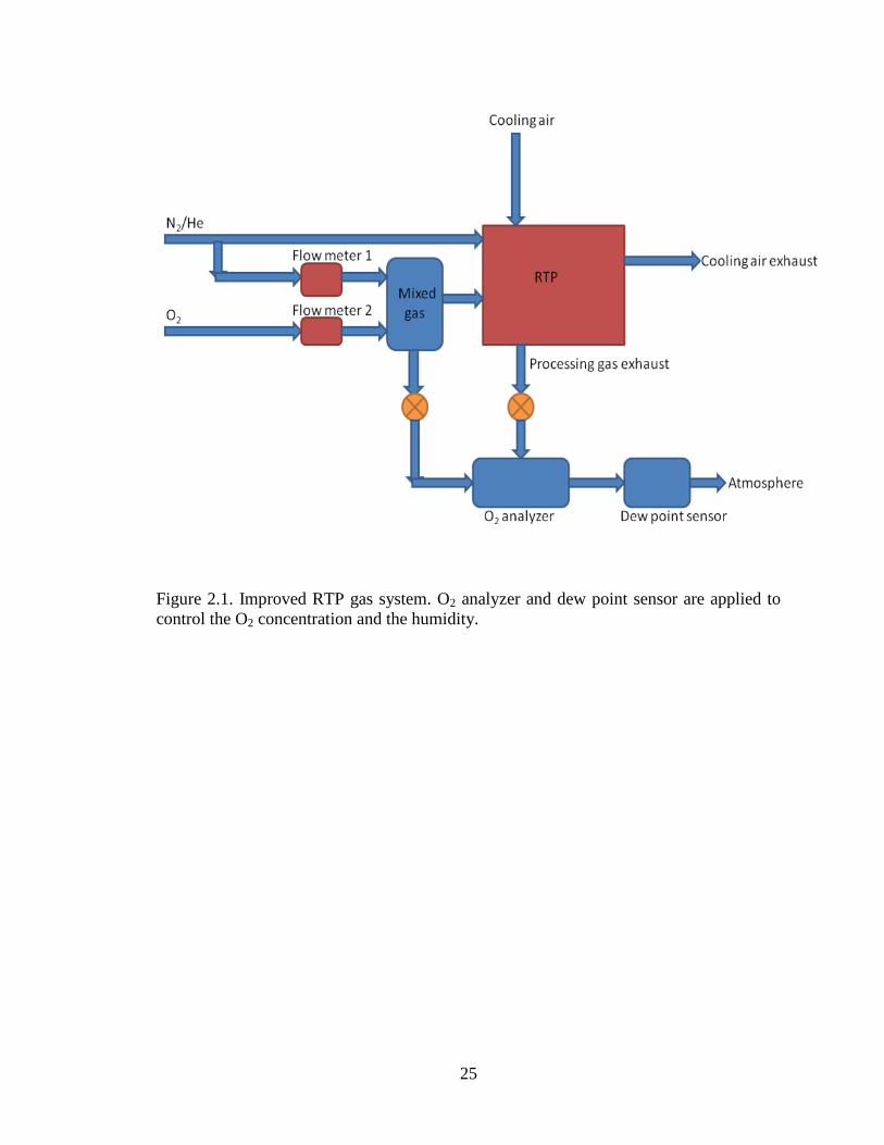
The concentration of O2 is measured using a trace O2 analyzer (Alpha Omega Series
3000, with a measure range of 1-10000 ppm), which can be connected both to the pro-
cessing gas input pipe and the output pipe. By monitoring the O2 concentration in these
pipes, we can exactly tell the O2 concentration in the chamber during the lateral heating
process. The O2 analyzer is followed by a dew point sensor, in order to control the hu-
midity in the chamber during the process. The schematic of the improved RTP gas sys-
tem is shown in figure 2.1.
2.4 Lift-off Process for Patterning of MOS Capacitors Gates
The MOS capacitors fabricated in our experiments are circles with diameter 100 µm. The
bi-layer resist photolithography and the lift-off process have been applied to pattern the
MOS capacitors gate, which have been reported in the publications of our lab be-
fore[49][50]
. The Shipley 1813 and the SU-8 2001 from Microchem serve as the positive
and negative photoresists. Since the SU-8 2001 developer (from Microchem) consists of
98% 1-Methoxy-2-propyl acetate (C6H12O3), which is a solvent for the S1813, no matter
whether the S1813 has went through exposure or not, an undercut structure could be
formed after the development. The schematic of the photolithography and lift-off process
is shown in figure 2.2, and the SEM image of the bilayer resist structure is shown in fig-
ure 2.3.
Page 33
23
In the previous work of our lab[39][40][41][42]
, Al was deposited by thermal evaporation
through shadow masks to form the MOS capacitor gate, in order to get rid of the photore-
sist. Post-metal annealing (PMA) was required to ensure low interface trap density and
good ohmic contact; without PMA, an air gap exists between the Al gate and the SiO2
dielectric, which decreases the accumulation region capacitance of the MOS capacitors.
However, Al is known to diffuse through ultrathin oxides (<30Å) at PMA temperatures
(~450°C), causing short-circuit of the devices.
Ni has excellent thermal stability (low/negligible diffusion through oxides at PMA tem-
perature). However, the melting temperature of Ni is high and it could only be deposited
by either e-beam evaporator or sputtering machine. Plasma in sputtering machine can
damage the ultrathin oxides by energetic ion bombardment, thus, e-beam evaporator is
chosen for Ni gate matallization, and a good metal gate thickness is 1000Å.
This photolithography and lift-off process for the Ni gate patterning has been working
effectively with low price; however, a drawback exists that there has always been the risk
of peeling off. We made the assumption that there are always organic remains after de-
velopment. In order to prove this assumption, samples with prolonged development time
were fabricated, and a phenomenon was observed that, while all samples show satisfacto-
ry undercut structures under microscope after photolithography, the longer the develop-
ment time is, the more severe the peeling off problem shows. Thus, the development pro-
cess must have left certain organic remains.
Page 34
24
2.5 Back-side contact and post metallization annealing
The back-side contact is made by a 1000Å Al film which is also deposited by e-beam
evaporator. During this process, the front-side of the sample is protected by hard baked
S1813.
The post metallization annealing is executed at 450°C in forming gas (N2:H2 = 10:1) for
30 minutes at a pressure of 1 atmosphere.
2.6 Current-Voltage, Capacitance-Voltage characteristics measurement
The capacitance-voltage characteristic is measured using a HP 4284A precision LCR me-
ter at 100 KHz, since the frequency dispersion is negligible, and the equipment is able to
provide measuring frequencies from 1 K to 1 MHz. The current-voltage characteristic is
measured using an Agilent 4155B semiconductor parameter analyzer.
The EOT and the flatband voltage of the capacitors are extracted from the C-V charac-
teristic via UC Berkeley Quantum-Mechanical Simulator (taking quantum correction into
consideration). The ideal C-V characteristic is simulated and used to fit the experimental
C-V characteristic. The current density is compared at the voltage VG=VFB+1.
Page 35
25
Figure 2.1. Improved RTP gas system. O2 analyzer and dew point sensor are applied to
control the O2 concentration and the humidity.
Page 36
26
Figure 2.2. The schematic of the photolithography and lift-off process.
Page 37
27
Figure 2.3. The SEM image of the bilayer resist undercut structure.
Page 38
28
Chapter 3 Wet Etch Process for Patterning of MOS Capacitors Gates
The drawbacks of lift-off process for MOS capacitors patterning is obvious: peeling off
problem requires that the photolithography parameters must be precisely controlled, oth-
erwise, even a tiny experiment condition change can cause severe problem. This intro-
duces unnecessary difficulty into the experiment operation. Plus, the peeling off problem
shows the contact between metal gate and dielectric material is not ideal, organic remains
exist between metal gate and dielectric material, which could affect electrical properties
of MOS capacitors.
Wet etching is another way to pattern MOS capacitors gate. In this situation, metal is
directly deposited onto dielectric layer without touching any organic solutions, so there
would be no gap between metal gate and dielectric material, and the contact is guaran-
teed. Several solutions have been reported as etchant for Ni, such as HCl: HNO3=5:1 so-
lution, HF: HNO3=1:1 solution, ect[51][52]
. However, a solution including acid could cause
damage to silicon oxide, which is unacceptable. FeCl3 solution is a satisfactory candidate
for our purpose, since it has the ability of etching Ni, while does not attack silicon oxide.
I started with 30% FeCl3 solution to work on our 1000Å Ni. S1813 was used to do pho-
tolithography. After exposure and development, the pattern areas are protected with pho-
toresist. Then sample are immersed into FeCl3 solution. The etching rate was so high that
all the Ni was etched away very fast. I started to dilute the FeCl3 solution. Although etch-
ing rate became lower, it was impossible to control the etching, severe undercut always
happened before Ni without photoresist protection is gone. After photoresist spincoating,
Page 39
29
a tiny gap could exist between photoresist and Ni, I assumed that FeCl3 solution could
flow into this gap and make a direct contact with Ni, which is supposed to be under pro-
tection. This gap could be fixed by hard bake of photoresist. Then hard bake was applied
on the sample after development (140°C for 3 minutes). However, this does not improve
this situation at all. The undercut problem is as serious with the hard baked sample as the
non-hard baked sample. If I etched samples until the un-protected part Ni is almost gone,
there is always undercut on the Ni pattern edge. This proves the gap between photoresist
and Ni is not the problem. Both the samples with and without photoresist hard bake are
shown in figure 3.1 and 3.2. After removing photoresist by Remover PG, we could see
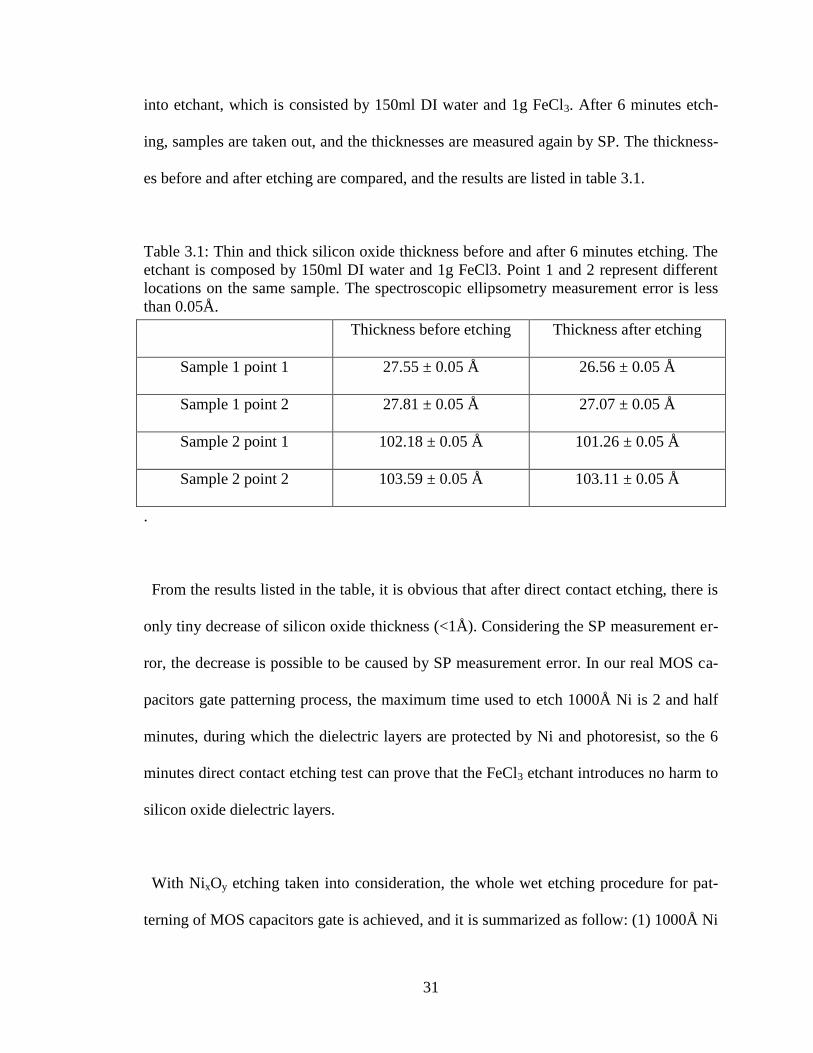
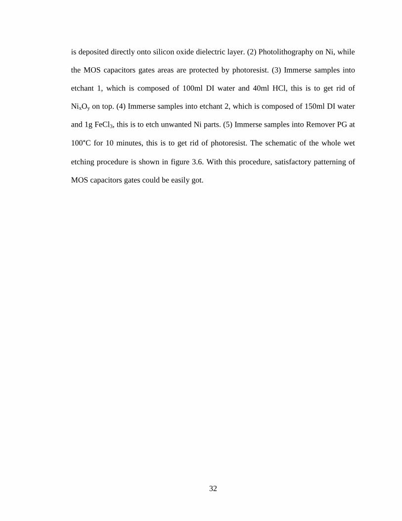
that the patterns are severely damaged, which is shown in figure 3.3.
Since the undercut problem was severe, either the etching rate of Ni by FeCl3 solution
must be still too high, or the etching time must be too long. Since the etching time was
already under 1 minute, the etching rate must be unacceptable. Does further dilution of
FeCl3 help? I immersed sample into further diluted FeCl3 sample, and it started to be very
difficult to get rid of Ni, even on the parts without photoresist protection. Then I used ul-
trasonic to help, and Ni started to peel off with huge sheets, which does not follow the
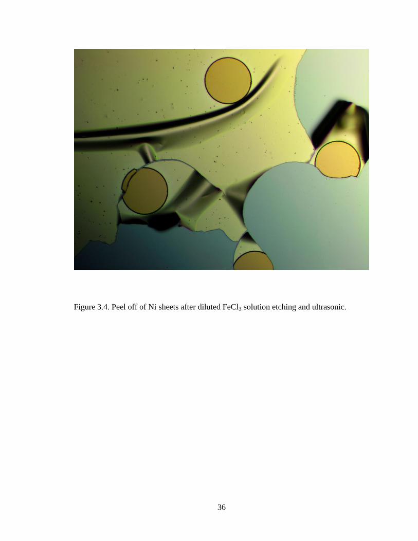
photolithography pattern at all. This is shown in figure 3.4. Thus, diluted FeCl3 solution
cannot provide satisfactory patterns.
Return to the situation with undercut. It is obvious that the Ni etching rate must be too
high, otherwise there cannot be undercut within 1 minute. But why there is always Ni re-
siduals on the parts without photoresist protection? Why Ni could not be etched uniform-
Page 40
30
ly; some areas totally gone, while other areas seem like totally untouched? We assume
this is because Ni is very easy to be oxidized, the top layer Ni directly contacts with oxy-
gen in the atmosphere, so a thin layer of NixOy exists above the metal layer after evapora-
tion. This thin layer of NixOy is not uniform among the whole sample surface, on the are-
as where this layer exists, the FeCl3 solution are blocked from touching Ni underneath;
on the other areas without this block, Ni is etched away fast. In order to prove this as-
sumption and get uniform etching among the whole sample, it is desirable to get rid of
this NixOy layer. Hydrochloric acid (HCl) solution provides an easy way to etch away
NixOy. Since this layer is thin, only low concentration and short time is needed. Based on
our experiment, 100ml DI water with 40ml HCl is able to etch away all NixOy in 1 mi-
nute. This solution has a really low etching rate on Ni, so over-etching does not need to
be worried.
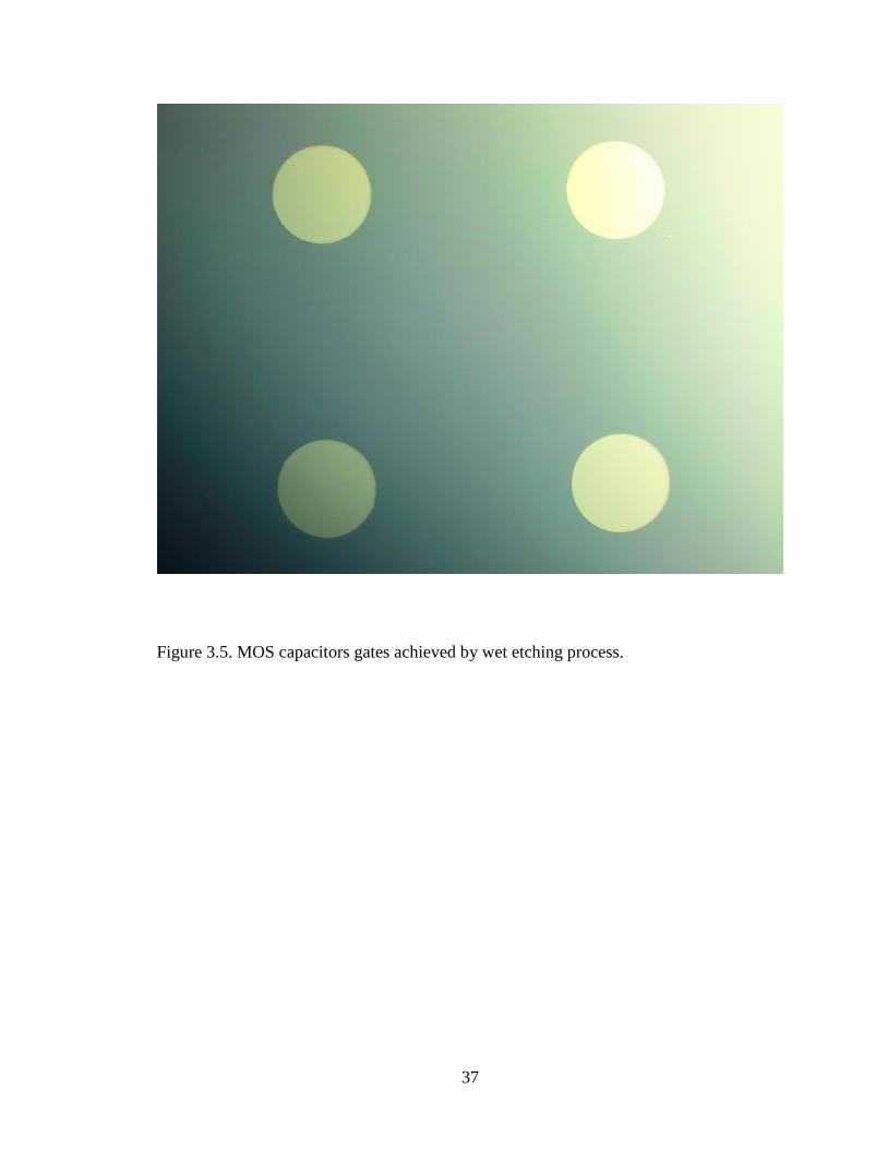
With HCl solution etching added before FeCl3 solution etching, satisfactory patterns are
achieved. The Ni under photoresist could maintain almost untouched, while the other Ni
are all gone. This is shown in figure 3.5, and the FeCl3 solution concentration which pro-
vides best result is 150ml DI water with 1g FeCl3. Higher concentration can result in a
little undercut.
Damage of silicon oxide is not acceptable, so experiment was done to prove that this
etchant does not affect silicon oxide. Both thin and thick silicon oxide are tested. Growth
of thin and think silicon oxide are demonstrated in 2.2. The original silicon oxide thick-
nesses are measured by spectroscopic ellipsometry (SP), and then samples are immersed
Page 41
31
into etchant, which is consisted by 150ml DI water and 1g FeCl3. After 6 minutes etch-
ing, samples are taken out, and the thicknesses are measured again by SP. The thickness-
es before and after etching are compared, and the results are listed in table 3.1.
Table 3.1: Thin and thick silicon oxide thickness before and after 6 minutes etching. The
etchant is composed by 150ml DI water and 1g FeCl3. Point 1 and 2 represent different
locations on the same sample. The spectroscopic ellipsometry measurement error is less
than 0.05Å.
Thickness before etching Thickness after etching
Sample 1 point 1 27.55 ± 0.05 Å 26.56 ± 0.05 Å
Sample 1 point 2 27.81 ± 0.05 Å 27.07 ± 0.05 Å
Sample 2 point 1 102.18 ± 0.05 Å 101.26 ± 0.05 Å
Sample 2 point 2 103.59 ± 0.05 Å 103.11 ± 0.05 Å
.
From the results listed in the table, it is obvious that after direct contact etching, there is
only tiny decrease of silicon oxide thickness (<1Å). Considering the SP measurement er-
ror, the decrease is possible to be caused by SP measurement error. In our real MOS ca-
pacitors gate patterning process, the maximum time used to etch 1000Å Ni is 2 and half
minutes, during which the dielectric layers are protected by Ni and photoresist, so the 6
minutes direct contact etching test can prove that the FeCl3 etchant introduces no harm to
silicon oxide dielectric layers.
With NixOy etching taken into consideration, the whole wet etching procedure for pat-
terning of MOS capacitors gate is achieved, and it is summarized as follow: (1) 1000Å Ni
Page 42
32
is deposited directly onto silicon oxide dielectric layer. (2) Photolithography on Ni, while
the MOS capacitors gates areas are protected by photoresist. (3) Immerse samples into
etchant 1, which is composed of 100ml DI water and 40ml HCl, this is to get rid of
NixOy on top. (4) Immerse samples into etchant 2, which is composed of 150ml DI water
and 1g FeCl3, this is to etch unwanted Ni parts. (5) Immerse samples into Remover PG at
100°C for 10 minutes, this is to get rid of photoresist. The schematic of the whole wet
etching procedure is shown in figure 3.6. With this procedure, satisfactory patterning of
MOS capacitors gates could be easily got.
Page 43
33
Figure 3.1. Undercut of Ni pattern after FeCl3 etching. Photoresist was hard baked after
photolithography.
Page 44
34
Figure 3.2. Undercut of Ni pattern after FeCl3 etching. Photoresist was not hard baked
after photolithography.
Page 45
35
Figure 3.3. Severe damaged Ni gate by undercut in FeCl3 solution etching process.
Page 46
36
Figure 3.4. Peel off of Ni sheets after diluted FeCl3 solution etching and ultrasonic.
Page 47
37
Figure 3.5. MOS capacitors gates achieved by wet etching process.
Page 48
38
Figure 3.6. The schematic of the wet etch process. Etchant 1: 100ml DI water with 40ml
HCl. Etchant 2: 150ml DI water with 1g FeCl3.
Page 49
39
Chapter 4 Rapid Thermal Process with Moisture
It has been reported that a SiO2 transition layer exists between Si and SiO2 in thermally
grown SiO2 film. Since SiO2 has a large volume expansion upon oxidation, Si at the in-
terface is under a tension and strained[53]
. This phenomenon looks similar to our experi-
ment situation. The SiO2 stated in the original paper was grown by wet oxidation. In or-
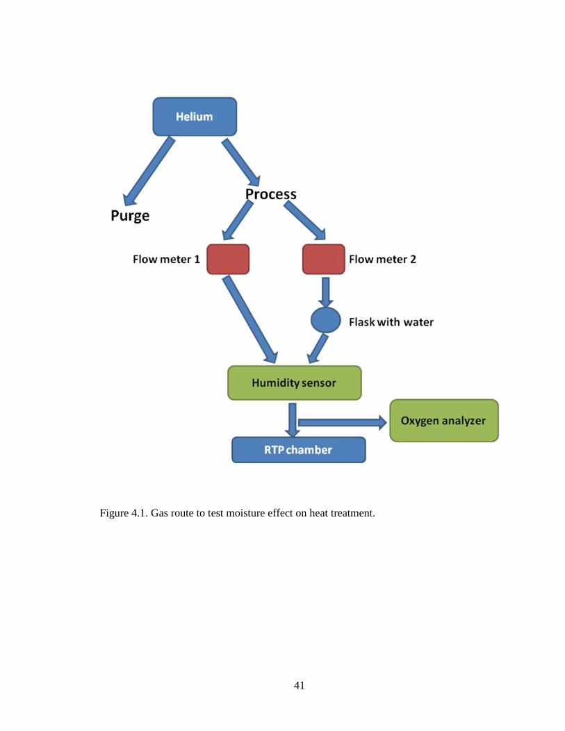
der to test the effect of moisture on the gate leakage current reduction, we re-built the gas
route of RTP system. This route is shown in figure 4.1.
Helium is used as processing gas, and trace O2 is replaced by moisture. This is realized
by flowing N2 through a flask with water inside. Pure He and He with moisture combine
together before entering into a humidity sensor, which is utilized to control the relative
humidity level. The mixture gas is then directed to RTP chamber, and trace O2 analyzer is
still applied to control the O2 concentration in the mixture gas.
A 4 inch Si wafer was used as substrate, and a quarter of 2 inch n-type Si wafer with
thermally grown ultrathin SiO2 is put onto this substrate. The temperature inside the RTP
chamber was increased with a rate of 10 °C/second, until it reached 1000°C, then hold for
60 seconds. 1000°C was chosen since it has been reported that in temperature higher than
1000°C, lattice distortion in Si substrate would reduce because of viscous flow of
SiO2[53]
. The relative humidity level was 50.1%.
After heat treatment, MOS capacitors were fabricated and tested, the capacitance densi-
ty-voltage (C-V) and current density-voltage (I-V) properties are shown in figure 4.2 and
Page 50
40
4.3. The flatband voltages (VFB) are consistent with all the control and RTP samples.
Equivalent oxide thickness (EOT) of control sample is less than 20Å, and RTP samples is
more than 24Å, which means after RTP, the ultrathin SiO2 got around 5Å regrowth.
From figure 4.3, it is obvious that after RTP, there is 3 orders of magnitude gate leakage
current density reduction. The 5Å regrowth of SiO2 dielectric layer corresponds to 2.5
order of magnitude reduction[16]
, and this should be substrated from the 3 orders. Taking
the SiO2 thickness increase into consideration, we could conclude that RTP is responsible
for 0.5 order of magnitude gate leakage current density reduction. This phenomenon is
uniform among all the devices in this sample, which is an effective way to provide MOS
devices with a little higher quality. However, 0.5 order is far less than our expected 3-5
order of magnitude gate leakage current reduction. The underlying mechanism for our
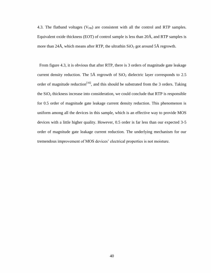
tremendous improvement of MOS devices’ electrical properties is not moisture.
Page 51
41
Figure 4.1. Gas route to test moisture effect on heat treatment.
Page 52
42
Figure 4.2. Capacitance density-voltage characteristics of n-type MOS capacitors before
and after rapid thermal process with moisture exists, flatband voltages and EOTs extract-
ed from the characteristics are marked.
Page 53
43
Figure 4.3. Current density-voltage characteristics of n-type MOS capacitors before and
after rapid thermal process with moisture exists.
Page 54
44
Chapter 5 Lateral Heating Process Experiments and Results
5.1 Background
At the beginning of the exploratory process, a 4’’ Si wafer was used in the RTP as the
substrate, and the test sample, which was a quarter of the 2’’ Si wafer, was put onto the
substrate. The temperature was raised to 1050°C~1080°C, and the holding time was in
the range of 10 seconds~4 minutes, changing depending on the thickness of the SiO2 lay-
er. Later we observed this specific trend: after several RTP heating processes, the 4’’ Si
substrate got bent near the centre point, making it convex, and the test sample was just
supported by the peak point of the substrate. The sample edge regions were suspending
above the substrate, and the MOS capacitors gate leakage current reduction is more likely
to be found in these hanging regions. The structure schematic is shown in figure 5.1.
SampleExcellent Results
at the Edge
4” Si Wafer as a Substrate Holder
Figure 5.1. Special condition when obvious gate leakage current reduction could be
available. After several times’ RTP, the 4’’ Si substrate became convex, and the good
results are available in the sample’s hanging edges.
The first assumption for explaining this phenomenon was that the cooling rate at the
hanging edges might be faster, which could brought structure changes. Dr. Chen and his
students found that a smaller Si substrate results a faster cooling rate. By changing the
Page 55
45
size of the Si substrate, they found out that once the cooling rate reaches 50°C/sec, which
could be easily achieved with the 4’’ Si substrate, there is no obvious improvement. The
cooling rate could not be a crucial factor for the good results at the hanging edges.
The second assumption was that the vertical non-uniform heating could brought struc-
ture changes, and the sample’s surface heating is supposed to be more than the inner bulk
heating. We applied the flash lamp annealing (FLA) on the samples. Since the FLA is a
vertically non-uniform heating only in milliseconds, it is able to heat only at the sample
surface, in a depth ranging from tens of micrometers to a few hundreds of micrometers.
Again, there is no obvious improvement comparing with the control sample. The vertical
non-uniform heating could not be a crucial factor, either.
The third assumption was that the lateral heat flow from the center contact region to
the hanging edge region might cause structure changes. To prove this hypothesis, several
experiments were designed, trying to imitate the hanging structure in figure 6.1, and to
enable better heat flow from contact region to hanging edge region. The results of these
experiments helped us to understand the underlying mechanism of the leakage current
reduction phenomenon.
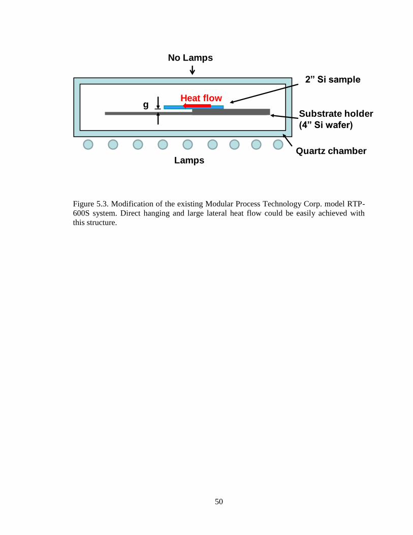
5.2 Effect of Direct Hanging and Heat Transportation
Based on the assumption that the key factor which brings the appealing electrical proper-
ties is the lateral heating from the contact region of the sample to the hanging edge re-
gion, a large enough heat flow must be guaranteed to arrive at the sample contact region.
Page 56
46
Meanwhile, if the sample does not have any other heat source, the heat arrives at the con-
tact region will definitely flow towards the hanging region. Thus the two requirements for
the RTP system are achieved: enough heat on the sample contact region, and no other
heat source for the whole sample.
If we could block the light radiation from the top of the RTP chamber, there would be
no other heat source for the sample, since sample does not directly receive any light. This
could be simply achieved by putting a 4’’ Si wafer above the quartz chamber.
If a step structure could be etched on the 4’’ Si substrate, the sample could be directly
hanged over the step. In this situation, only one contact interface for the heat flow exists.
More heat generated on the 4’’ Si substrate would arrive at the sample contact region. Si
could be etched with tetramethylammonium hydroxide (TMAH) solution, and SiO2 is a
perfect material for etching mask[54][55][56]
. SiO2 could be easily patterned with traditional
photolithography and HF etching. The schematic for this procedure is shown in figure
5.2.
The improved lateral heating process positioning is illustrated in figure 5.3. The heat
originates from the 4’’ Si substrate, and directly flows into the hanging sample. Satisfac-
tory lateral heating flow is now under control.
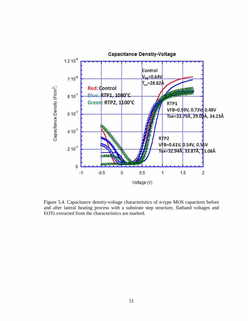
Ultrathin silicon oxide samples are thermally grown as stated in 2.2. The lateral heating
process was executed in N2 and O2 mixture environment. One sample was processed at
Page 57
47
1080°C for 10 seconds, and the other sample was processed at 1100°C for 10 seconds.
Both of the samples went through a temperature increase rate of 10°C/second. For
1080°C sample, the O2 concentration was between 220 ppm to 250 ppm; for 1100°C
sample, the O2 concentration was around 195 ppm.
The control sample, which means silicon oxide which did not go through heat treatment,
has an equivalent oxide thickness (EOT) of 28.82Å, and the gate leakage current density
is 0.07A/cm2. This gate leakage current density is higher than simulated gate leakage cur-
rent density of the ideal SiO2 with similar thickness, and we assume contamination as the
reason. The flatband voltage shift of the control sample from the ideal value also supports
this assumption.
After lateral heating process, both of the silicon oxide samples got regrowth. The re-
growth was 3-4Å in hanging region, and 0-1Å in contact region. According to ideal SiO2
gate leakage current density simulation, 3-4Å increase in thickness corresponds to 1.5 to
2 order of magnitude leakage current density reduction[16]
.
The capacitance density-voltage (CV) and current density-voltage (IV) curves of the
MOS capacitors are exhibited in figure 5.4 and 5.5. From the IV curve, it is obvious that
there is huge gate leakage current density reduction after heat treatment. Part of the rea-
son is that the heat treatment improves silicon oxide quality, and gets rid of contamina-
tion. Comparing the gate leakage current density with ideal simulation value, there is still
1-2 order of magnitude reduction, which is believed to be introduced by the lateral heat-
Page 58
48
ing process.
However, the gate leakage current density reduction is not uniform. From the experi-
ment results, there is not any principle which shows how the locations of MOS capacitors
with appealing electrical properties distribute among the whole sample. Gate leakage cur-
rent density reduction phenomenon just appears randomly. This implies the lateral heat-
ing effect is not uniform with this experiment condition. The reason might be: the light
radiation comes from bottom linear tungsten-halogen lamps is reflected by surfaces in-
side RTP chamber, in this way, some light could still arrive at sample surface, which pro-
vides an energy source, and could be a disturbance to the lateral heat flow from contact
region to hanging region.
Page 59
49
Figure 5.2. The schematic of Si step structure etching by TMAH.
Page 60
50
gSubstrate holder
(4” Si wafer)
2” Si sample
No Lamps
LampsQuartz chamber
Heat flow
Figure 5.3. Modification of the existing Modular Process Technology Corp. model RTP-
600S system. Direct hanging and large lateral heat flow could be easily achieved with
this structure.
Page 61
51
Figure 5.4. Capacitance density-voltage characteristics of n-type MOS capacitors before
and after lateral heating process with a substrate step structure, flatband voltages and
EOTs extracted from the characteristics are marked.
Page 62
52
Figure 5.5. Current density-voltage characteristics of n-type MOS capacitors before and
after lateral heating process with a substrate step structure, gate leakage current densities
at V=VFB+1 are marked.
Page 63
53
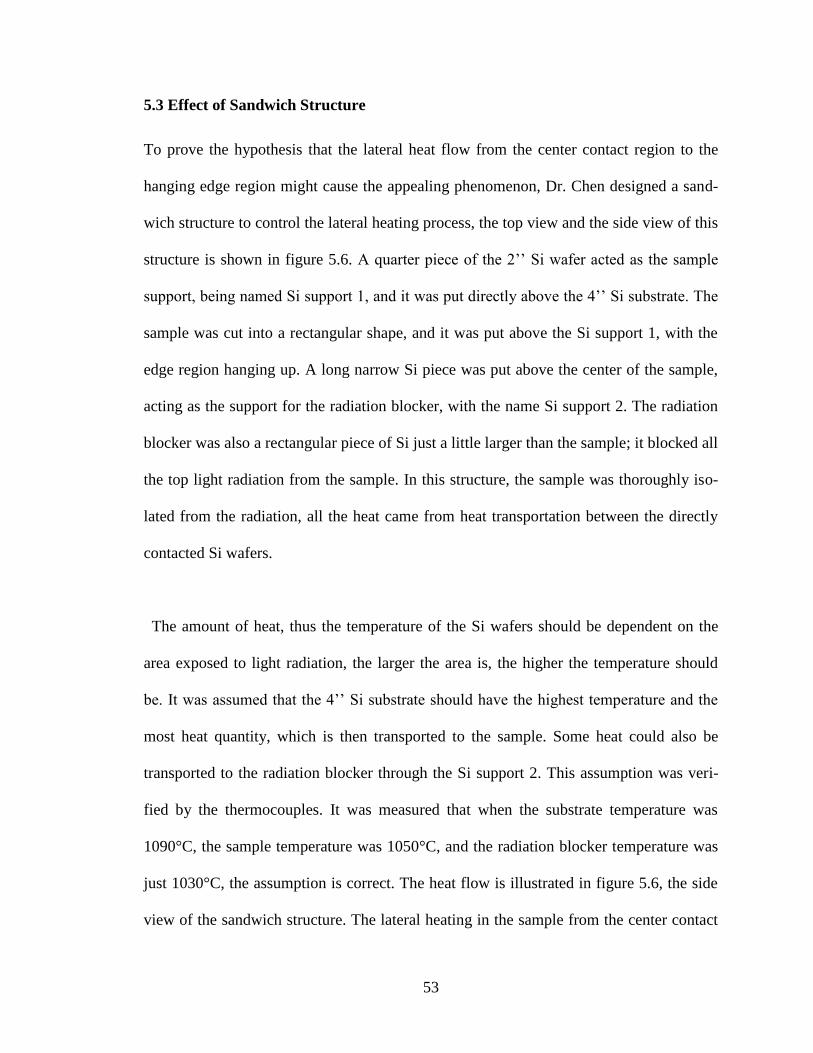
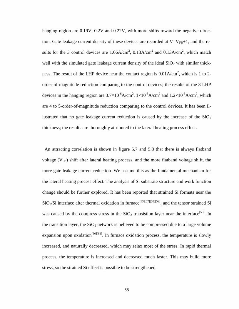
5.3 Effect of Sandwich Structure
To prove the hypothesis that the lateral heat flow from the center contact region to the
hanging edge region might cause the appealing phenomenon, Dr. Chen designed a sand-
wich structure to control the lateral heating process, the top view and the side view of this
structure is shown in figure 5.6. A quarter piece of the 2’’ Si wafer acted as the sample
support, being named Si support 1, and it was put directly above the 4’’ Si substrate. The
sample was cut into a rectangular shape, and it was put above the Si support 1, with the
edge region hanging up. A long narrow Si piece was put above the center of the sample,
acting as the support for the radiation blocker, with the name Si support 2. The radiation
blocker was also a rectangular piece of Si just a little larger than the sample; it blocked all
the top light radiation from the sample. In this structure, the sample was thoroughly iso-
lated from the radiation, all the heat came from heat transportation between the directly
contacted Si wafers.
The amount of heat, thus the temperature of the Si wafers should be dependent on the
area exposed to light radiation, the larger the area is, the higher the temperature should
be. It was assumed that the 4’’ Si substrate should have the highest temperature and the
most heat quantity, which is then transported to the sample. Some heat could also be
transported to the radiation blocker through the Si support 2. This assumption was veri-
fied by the thermocouples. It was measured that when the substrate temperature was
1090°C, the sample temperature was 1050°C, and the radiation blocker temperature was
just 1030°C, the assumption is correct. The heat flow is illustrated in figure 5.6, the side
view of the sandwich structure. The lateral heating in the sample from the center contact
Page 64
54
region to the hanging edge region is realized.
The lateral heating process was executed in He and O2 mixture environment, while the
O2 concentration was maintained around 195 ppm. The dew point value was -54.2°C,
which means the humidity was low enough that it would not bring any regrowth effect.
The sample’s position in the RTP chamber during the lateral heating process was the
same with that displayed in figure 6.6. The lateral heating was processed at 1060°C for 10
seconds, and the temperature increase rate was 10 °C/second.
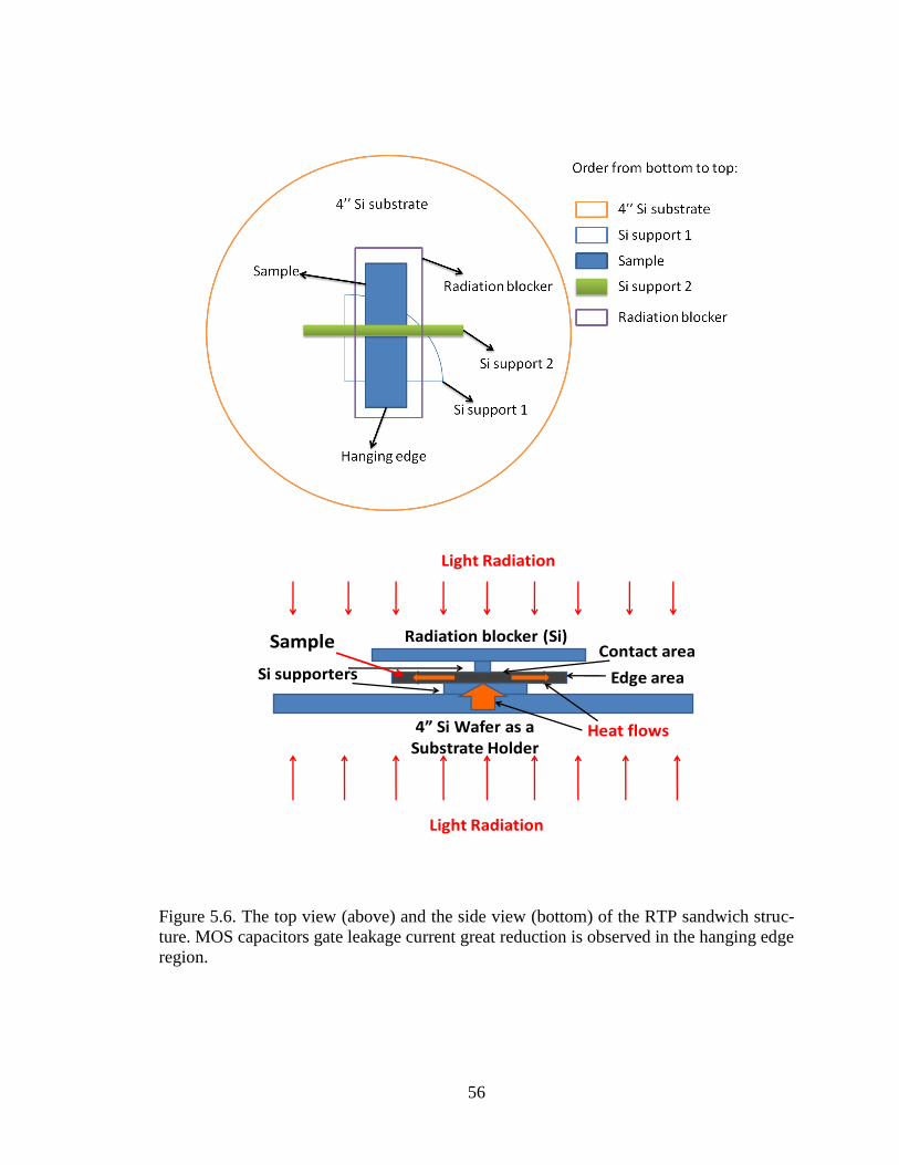
There was no obvious SiO2 thickness increase after the lateral heating process. As
marked in figure 5.7, the EOT for the 3 control devices are 23.4Å, 22.9Å, and 22.2Å; the
EOT for the LHP device near the contact region is 23.3Å; the EOT for the 3 LHP devices
in the hanging region are 22.4Å, 23.2Å, and 23.7Å. With this limitation of the SiO2 re-
growth, which was achieved by precise control of the O2 concentration, all the leakage
current reduction could be attributed to lateral heating process effect.
There is a correlation between the flatband voltage shift and the leakage current reduc-
tion is clearly illustrated in figure 5.7 and 5.8. The flatband voltages of the 3 control de-
vices serve as the reference flatband voltages, and the values are 0.65V, 0.68V, and
0.71V. The deviation from the theoretically calculated flatband voltage (0.85V) is as-
signed to the contamination during the fabrication process. The flatband voltage of the
LHP device near the contact region is 0.38V, with a slight shift toward the negative direc-
tion comparing to the control devices. The flatband voltages of the 3 LHP devices in the
Page 65
55
hanging region are 0.19V, 0.2V and 0.22V, with more shifts toward the negative direc-
tion. Gate leakage current density of these devices are recorded at V=VFB+1, and the re-
sults for the 3 control devices are 1.06A/cm2, 0.13A/cm
2 and 0.13A/cm
2, which match
well with the simulated gate leakage current density of the ideal SiO2 with similar thick-
ness. The result of the LHP device near the contact region is 0.01A/cm2, which is 1 to 2-
order-of-magnitude reduction comparing to the control devices; the results of the 3 LHP
devices in the hanging region are 3.7×10⁻⁶
A/cm2, 1×10
-6A/cm
2 and 1.2×10
-6A/cm
2, which
are 4 to 5-order-of-magnitude reduction comparing to the control devices. It has been il-
lustrated that no gate leakage current reduction is caused by the increase of the SiO2
thickness; the results are thoroughly attributed to the lateral heating process effect.
An attracting correlation is shown in figure 5.7 and 5.8 that there is always flatband
voltage (VFB) shift after lateral heating process, and the more flatband voltage shift, the
more gate leakage current reduction. We assume this as the fundamental mechanism for
the lateral heating process effect. The analysis of Si substrate structure and work function
change should be further explored. It has been reported that strained Si formats near the
SiO2/Si interface after thermal oxidation in furnace[53][57][58][59]
, and the tensor strained Si
was caused by the compress stress in the SiO2 transistion layer near the interface[53]
. In
the transition layer, the SiO2 network is believed to be compressed due to a large volume
expansion upon oxidation[60][61]
. In furnace oxidation process, the temperature is slowly
increased, and naturally decreased, which may relax most of the stress. In rapid thermal
process, the temperature is increased and decreased much faster. This may build more
stress, so the strained Si effect is possible to be strengthened.
Page 66
56
Sample
Light Radiation
4” Si Wafer as a Substrate Holder
Radiation blocker (Si)
Light Radiation
Si supporters
Heat flows
Contact area
Edge area
Figure 5.6. The top view (above) and the side view (bottom) of the RTP sandwich struc-
ture. MOS capacitors gate leakage current great reduction is observed in the hanging edge
region.
Page 67
57
Figure 5.7. Capacitance density-voltage characteristics of the n-type MOS capacitors be-
fore and after lateral heating process, flatband voltages and EOTs extracted from the
characteristics are marked.
Page 68
58
Figure 5.8. Current density-voltage characteristics of the same MOS capacitors. There is
4 to5-order-of-magnitude gate leakage current reduction after the lateral heating process.
Page 69
59
Chapter 6 Conclusion and Future Work
6.1 Conclusion
An appealing improvement of MOS capacitors electrical property has been achieved. By
applying lateral heating process on Si wafer with thermally grown ultrathin SiO2 (~20Å),
the gate leakage current density of MOS capacitors could be reduced by 3-5 order of
magnitude. Since unacceptable gate leakage current is one of the main reasons which
prevent the scaling development trend in semiconductor industry, this technology brings
a possibility to postpone the end of scaling trend, and pave a way for extensive applica-
tion in industry.
The underlying mechanism of this appealing phenomenon has been explored. After lat-
eral heating process, the flatband voltage of MOS capacitors shifts to negative direction.
This is probably due to strained Si at the SiO2/Si interface, which is induced by the com-
press stress in the SiO2 transition layer. Rapid increasing and decreasing of temperature
in RTP prevent the stress relaxation, and strengthen the effect.
A new method for pattering of MOS capacitors metal gate has been developed, and lift-
off process has been replaced by wet etching process. This method provides better con-
tact between dielectric layer and metal gate, meanwhile the operation is much easier.
6.2 Future Work
Dielectric materials with higher dielectric constants (high-k materials) have already over-
Page 70
60
came SiO2 and became the dominant dielectric materials in semiconductor field. Since
the underlying mechanism for our appealing finding might be Si structure change, not
SiO2 structure change, it is reasonable to assume that this effect could be applied on high-
k gate oxide stacks to reduce the gate tunneling leakage current. In the future, it is valua-
ble to demonstrate the validity of the lateral heating process for improving the high-k gate
oxide stacks comparable to those in industry. If the validity could be proved, this tech-
nology would be able to further improve the properties of the silicon MOS devices, and
pave a way for extensive application of this technology in industry.
Page 71
61
Reference
[1] I. M. Ross, “The invention of the transistor,” proceedings of the IEEE, vol. 86, no. 1,
pp. 7-28, 1998.
[2] W. Shockley, Electrons and Holes in Semiconductors. New York: Van Nostrand,
1950.
[3] D. Kahng and M. M. Attala, “Silicon-Silicon Dioxide Surface Device,” IRE Device
Research Conference, Pittsburg, 1960.
[4] G. E. Moore, “Cramming more components onto integrated circuits,” Electronics, pp.
113-117, April 19, 1965.
[5] G. E. Moore, “Progress in digital integrated electronics,” International Electron De-
vice Meeting, IEEE, pp. 11-13, 1975.
[6] Wikipedia, Moore’s Law, http://en.wikipedia.org/wiki/Moore's_law.
[7] The International Technology Roadmap for Semiconductors (ITRS), 2010 edition.
[8] D. L. Critchlow, “MOSFET scaling-the driver of VLSI technology,” IEEE Proc., vol.
87, pp. 659, 1999.
[9] J. Singh, Semiconductor Devices: Basic Principles. New York: John Wiley & Sons,
2001.
[10] R. H. Dennard, F. H. Gaensslen, etc, “Design of ion-implanted MOSFETs with very
small physical dimensions,” IEEE J. Solid-State Circuits SC-9, pp. 256-268, 1974.
[11] W. Haensch, E. J. Nowak, etc, “Silicon CMOS devices beyond scaling,” IBM Jour-
nal of Research and Development, vol. 50, no. 4/5, pp. 339-361, 2006.
[12] S. Thompson, P. Packan, etc, “Mos scaling: transistor challenges for the 21st centu-
ry,” Intel Technol. J., Q3, 1998.
[13] “Technology backgrounder: high-k gate oxides”, icknowledge.com.
[14] K. Roy, S. Mukhopadhyay, etc, “Leakage current mechanisms and leakage reduction
techniques in deep-submicrometer CMOS circuits,” proceedings of the IEEE, vol. 91,
no.2, pp. 305-327, 2003.
[15] Pang Leen Ong, “Phonon-energy-coupling-enhancement effects and its application,”
PhD dissertation, University of Kentucky, 2008.
[16] S. H. Lo, D. A. Buchanan, etc, “Quantum-mechanical modeling of electron tunnel-
ing current from the inversion layer of ultra-thin-oxide nMOSFET’s,” IEEE Electron De-
vice Letters, vol. 18, pp. 209-211, 1997.
[17] G. D. Wilk, R. M. Wallace, etc, “High-k gate dielectrics: current status and materials
properties consideration,” Applied Physics Review, vol. 89, num. 10, pp. 5243-5275,
2001
[18] K. Henson, H. Bu, etc, “Gate length scaling and high drive currents enabled for high
performance SOI technology using high-k/metal gate,” IEDM, pp. 645-648, 2008.
[19] M. Takahashi, A. Ogawa, etc, “Gate-first processed FUSI/HfO2/HfSiOx/Si
MOSFETs with EOT=0.5 nm,” IEDM, pp. 523-526, 2007.
[20] T. Ando, M. M. Frank, etc, “Ultimate EOT scaling (< 5Å) using Hf-based high-k
gate dielectrics and impact on carrier mobility,” ECS Transactions, vol. 28, no. 1, pp.
115-123, 2010.
[21] B. Hoeneisen, C. A. Mead, “Fundamental limitations in microelectronics-I. MOS
technology,” solid state electronics, vol. 15, pp. 819-829, 1972.
[22] J. T. Wallmark, “Fundamental physical limitations in integrated electronic circuits,”
Page 72
62
Inst. Phys. Conf. Ser., No. 25, pp. 133-167, 1975
[23] C. Hu, “Gate oxide scaling limits and projections,” IEDM tech. Digest, pp. 96-99,
1996.
[24] J. H. Stathis, D. J. Dimaria, “Reliability projection for ultra-thin oxides at low volt-
age,” IEDM tech. Digest, pp. 167-170, 1998.
[25] L. Chang, Y. Choi, etc, “Extremely scaled silicon nano-CMOS devices,” Proceed-
ings of the IEEE, vol. 91, no. 11, pp. 1860-1873, 2003.
[26] M. Kanellos, “Intel scientists find wall for Moore’s Law,” CENT, December 01,
2003.
[27] I. Vurgaftman, J. R. Meyer, etc, “Band parameters for III-V compound
semiconductors and their alloys,” Journal of Applied Physics, vol. 89, no. 11, pp. 5815-
5875, 2001.
[28] S. Iijima, “Helical microtubules of graphitic carbon,” Nature, vol. 354, pp. 56-68,
1991.
[29] P. Avouris, “Supertubes,” IEEE spectrum, vol. 41, no. 8, pp. 40-45, 2004.
[30] N. S. Hush, “An overview of the first half-century of molecular electronics,” Annals
of the New York Academy of Sciences, vol. 1006, issue 1, pp. 1-20, 2003.
[31] S. A. Wolf, D. D. Awschalom, etc, “Spintronics: a spin-based electronics vision for
the future,” Science, vol. 294, pp. 1488-1495, 2001.
[32] K. K. Likharev, “Single-electron devices and their applications,” Proceeding of the
IEEE, vol. 87, no. 4, pp. 606-632, 1999.
[33] J. W. Lyding, K. Hess, etc, “Reduction of hot electron degradation in metal oxide
semiconductor transistors by deuterium processing,” Applied Physics Letters, vol. 68, pp.
2526-2528, 1996.
[34] P. J. Chen, R. M. Wallace, “Examination of deuterium transport through device
structure,” Applied Physics Letters, vol 73, pp. 3441-3443, 1998.
[35] R. A. B. Devine, J. L. Autran, etc, “Interfacial hardness enhancement in deuterium
annealed 0.25 µm channel metal oxide semiconductor transistors,” Applied Physics Let-
ters, vol 70, pp. 2999-3001, 1997.
[36] C. G. Van de Walle, W. B. Jackson, “Reduction of hot electron degradation in metal
oxide semiconductor transistors by deuterium processing-comment,” Applied Physics
Letters,vol. 69, pp. 2441, October, 1996.
[37] J. H. Wei, M. S. Sun, etc, “A possible mechanism for improved light-induced degra-
dation in deuterated amorphous silicon alloy,” Applied Physics Letters, vol. 71, pp. 1498-
1500, 1997.
[38] Z. Chen, J. Guo, etc, “Evidence for energy coupling from the Si-D vibration mode to
the Si-Si and Si-O vibration modes at the SiO2/Si interface,” Applied Physics Letters, vol.
83, pp. 2151-2153, 2003.
[39] Z. Chen, J. Guo, “Dramatic enhancement of phonon energy coupling at the SiO2/Si
interface due to rapid thermal processing of the gate oxide,” presentation at the 35th
IEEE
Semiconductor Interface Specialists Conf., San Diego, CA, December 9th
-11th
, 2004.
[40] Z. Chen, J. Guo, and F. Q. Yang, “Phonon-energy-coupling enhancement: strength-
ening the chemical bonds of the SiO2/Si system,” Applied Physics Letters, vol. 88, pp.
082905, 2006.
[41] Z. Chen, J. Guo, “Dramatic reduction of gate leakage current of ultrathin oxides
through oxide structure modification,” Solid-State Electronics, vol. 50, pp. 1004-1011,
Page 73
63
2006.
[42] Z. Chen, “Mechanism for generation of the phonon-energy-coupling enhancement
effect for ultrathin oxides on silicon,” Applied Physics Letters, vol. 91, pp. 223513, 2007.
[43] Z. Chen, J. Guo, and P. Ong, “Fundamental mechanisms for reduction of leakage
current of silicon oxide and oxynitride through RTP-induced phonon-energy coupling,”
Proc. 14th
annual IEEE international conference on advanced thermal processing of sem-
iconductors – RTP2006, Kyoto, Japan, October 10th
-13th
, 2006 (invited).
[44] P. Ong, Z. Chen, “Evidence of enhanced phonon-energy coupling in SiO2/Si,” Ap-
plied Physics Letters, vol. 90, pp. 113516, 2007.
[45] T. H. Hou, J. Gutt, etc, “Improved scalability of high-k gate dielectrics by using Hf-
Aluminates,” Electrochemical Society Meeting, Salt Lake City, Utah, Abstract No. 384,
2002.
[46] W. Kern, D. A. Putotinen, “Cleaning solutions based on hydrogen peroxide for use
in silicon semiconductor technology,” RCA Review, vol. 31, pp. 187, 1970.
[47] W. Kern, “Handbook of Semiconductor Wafer Cleaning Technology,” William An-
drew Publishers, 1993.
[48] B. E. Deal, A. S. Grove, “General relationship for the thermal oxidation of silicon,”
Journal of Applied Physics, vol. 36, issue 12, pp. 3770-3778, 1965.
[49] P. L. Ong, Z. Chen, etc, “Large leakage-cuurent reduction of ultrathin industrial
SiON wafers induced by phonon-energy-coupling enhancement.” Electrochem. Solid-
State Letters, vol. 11, no. 11, pp. 293-295, 2008.
[50] Z. Chen, P. L. Ong, etc, “Reliable observation of large leakage-current reduction of
thin SiO2 induced by phonon-energy-coupling enhancement: problems and solution,” J.
Electrochem. Soc., vol. 157, pp. 44-48, 2010.
[51] Wet Etching Recipes, http://www.siliconfareast.com/etch_recipes.htm
[52] K. R. Williams, K. Gupta, etc, “Etch rates for micromachining processing-part 2,”
Journal of Microelectromechanical Systems, vol. 12, no. 6, pp. 761-778, 2003.
[53] K. Nakajima, M. Suzuki, etc, “Lattice Distortion at SiO2/Si(001) interface studied
with high-resolution Rutherford backscattering spectroscopy/channeling,” Japanese
Journal of Applied Physics, vol. 45, no. 4A, pp. 2467-2469, 2006.
[54] J. T. L. Thong, W. K. Choi, etc, “TMAH etching of silicon and the interaction of
etching parameters,” Sensors and Actuators A, vol. 63, pp. 243-249, 1997.
[55] P. H. Chen, H. Y. Peng, etc, “The characteristic behavior of TMAH water solution
for anisotropic etching on both silicon substrate and SiO2 layer,” Sensors and Actuators
A, vol. 93, pp. 132-137, 2001.
[56] K. Biswas, S. Kal, etc, “Etch characteristics of KOH, TMAH and dual doped TMAH
for bulk micromachining of silicon,” Microelectronics Journal, vol. 37, pp. 519-525,
2006.
[57] Y. P. Kim, S. K. Choi, etc, “Direct observation of Si lattice strain and its distribution
in the Si(001)-SiO2 interface transition layer,” Applied Physics Letters, vol. 71, pp. 3504-
3506, 1997.
[58] N. V. Nguyen, D. ChandlerHorowitz, etc, “Spectroscopic ellipsometry determination
of the properties of the thin underlying strained Si layer and the roughness at SiO2/Si in-
terface,” Applied Physics Letters, vol. 64, pp. 2688-2690, 1994.
[59] W. Daum, H. –J. Krause, etc, “Identification of strained silicon layers at Si-SiO2 in-
terfaces and clean Si surface by nonlinear optical spectroscopy,” Physical Review Letters,
Page 74
64
vol. 71, no. 8, pp. 1234-1237, 1993.
[60] Y. Sugita, S. Watanabe, etc, “Structural fluctuation of SiO2 network at the interface
with Si,” Applied Surface Science, 100/101, pp. 268-271, 1996.
[61] S. Miyazaki, H. Nishimura, etc, “Structure and electronic states of ultrathin SiO2
thermally grown on Si(100) and Si(111) surfaces,” Applied Surface Science, 113/114, pp.
585-589, 1997.
Page 75
65
Vita
Lei Han was born in Taigu County, Shanxi Province, P. R. China on September 27th
,
1985.
Education
August, 2008 --- Present
Ph. D. Student
Department of Electrical and Computer Engineering, University of Kentucky,
September, 2003 --- July, 2007
Bachelor of Engineering
College of Precision Instrument and Opto-Electronics Engineering,
Tianjin University, P. R. China
Bachelor of Management (Minor)
College of Management, Tianjin University, P. R. China
Awards
RCTF (Research Challenge Trust Fund) Research Scholarship, University of Kentucky,
Lexington, KY, 2011-2012
RCTF (Research Challenge Trust Fund) Fellowship, University of Kentucky, Lexington,
KY, 2011-2012
3A Student Scholarship, Tianjin University, Tianjin, China, 2004-2007
Publications
“The interfacial quality of HfO2 on silicon with different thicknesses of the chemical ox-
ide interfacial layer”, S.B.Li, L.Han and Z.Chen, Journal of The Electrochemical Society,
vol. 157, pp221-224, 2010.
“Lateral heating of SiO2/Si: interfacial Si structure change causing tunneling current re-
duction”, Z. Chen, P. Ong, Y. Wang, L. Han, Applied Physics Letter, vol. 100, pp. 171602
1-4, 2012.