1 IntroductionThe i.MX 6SoloLite processor represents Freescale’s latest achievement in integrated multimedia applications processors, which are part of a growing family of multimedia-focused products that offer high performance processing and are optimized for lowest power consumption.
The processor features Freescale’s advanced implementation of the a single ARM® Cortex®-A9 MPCore™ multicore processor, which operates at speeds up to 1 GHz. It includes 2D graphics processor and integrated power management. The processor provides a 32-bit DDR3-800 memory interface and a number of other interfaces for connecting peripherals, such as WLAN, Bluetooth™, GPS, hard drive, displays, and camera sensors.
The i.MX 6SoloLite processor is specifically useful for applications, such as:
• Color and monochrome eReaders
• Entry level tablets
• Barcode scanners
i.MX 6SoloLite Applications Processors for Consumer Products
i.MX 6SoloLite Applications Processors for Consumer Products, Rev. 3
2 Freescale Semiconductor
Introduction
The i.MX 6SoloLite processor features:
• Applications processor—The processor enhances the capabilities of high-tier portable applications by fulfilling the ever increasing MIPS needs of operating systems and games. Freescale’s Dynamic Voltage and Frequency Scaling (DVFS) provides significant power reduction, allowing the device to run at lower voltage and frequency with sufficient MIPS for tasks, such as audio decode.
• Multilevel memory system—The multilevel memory system of each processor is based on the L1 instruction and data caches, L2 cache, and internal and external memory. The processor supports many types of external memory devices, including DDR3, low voltage DDR3, LPDDR2, NOR Flash, PSRAM, cellular RAM, and managed NAND, including eMMC up to rev 4.4/4.41.
• Smart speed technology—The processor has power management throughout the IC that enables the rich suite of multimedia features and peripherals to consume minimum power in both active and various low power modes. Smart speed technology enables the designer to deliver a feature-rich product, requiring levels of power far lower than industry expectations.
• Dynamic voltage and frequency scaling—The processor improves the power efficiency of devices by scaling the voltage and frequency to optimize performance.
• Multimedia powerhouse—The multimedia performance of each processor is enhanced by a multilevel cache system, NEON™ MPE (Media Processor Engine) co-processor, and a programmable smart DMA (SDMA) controller.
• Powerful graphics acceleration—Each processor provides three independent, integrated graphics processing units: 2D BLit engine, a 2D graphics accelerator, and dedicated OpenVG™ 1.1 accelerator.
• Interface flexibility—The processor supports connections to a variety of interfaces: LCD controller, CMOS sensor interface (parallel), high-speed USB on-the-go with PHY, high-speed USB host PHY, multiple expansion card ports (high-speed MMC/SDIO host and other), 10/100 Mbps Ethernet controller, and a variety of other popular interfaces (such as UART, I2C, and I2S serial audio).
• Electronic Paper Display Controller—The processor integrates EPD controller that supports E-INK color and monochrome with up to 2048 x 1536 resolution at 106 Hz refresh, 4096 x 4096 resolution at 20 Hz refresh and 5-bit grayscale (32-levels per color channel).
• Advanced security—The processor delivers hardware-enabled security features that enable secure e-commerce, digital rights management (DRM), information encryption, secure boot, and secure software downloads. The security features are discussed in detail in the i.MX 6SoloLite security reference manual (IMX6SLSRM). Contact your local Freescale representative for more information.
• Integrated power management—The processor integrates linear regulators and generate internally all the voltage levels for different domains. This significantly simplifies system power management structure.
• GPIO with interrupt capabilities—The new GPIO pad design supports configurable dual voltage rails at 1.8V and 3.3V supplies. The pad is configurable to interface at either voltage level.
Introduction
i.MX 6SoloLite Applications Processors for Consumer Products, Rev. 3
Freescale Semiconductor 3
1.1 Ordering InformationTable 1 shows the orderable part numbers covered by this data sheet. Table 1 does not include all possible orderable part numbers. The latest part numbers are available on freescale.com/imx6series. If your desired part number is not listed in Table 1, or you have questions about available parts, see freescale.com/imx6series or contact your Freescale representative.
Figure 1 describes the part number nomenclature so that users can identify the characteristics of the specific part number they have (for example, Cores, Frequency, Temperature Grade, Fuse options, Silicon revision).
Ensure that you have the right data sheet for your specific part by checking the Temperature Grade (Junction) field and matching it to the right data sheet. If you have questions, see freescale.com/imx6series or contact your Freescale representative.
Table 1. Example Orderable Part Numbers
Part Number Mask Set OptionsSpeedGrade
Temperature(Tj)
Package1
1 Case 2240 is RoHS compliant, lead-free MSL (moisture sensitivity level) 3.
— 16-bit, and 32-bit DDR3-800, and LPDDR2-800 channels
— 16/32-bit NOR Flash.
— 16/32-bit PSRAM, Cellular RAM (32 bits or less)
Each i.MX 6SoloLite processor enables the following interfaces to external devices (some of them are muxed and not available simultaneously):
• Displays—Total three interfaces are available.
— LCD, 24bit display port, up to 225 Mpixels/sec (for example, WUXGA at 60 Hz)
— EPDC, color, and monochrome E-INK, up to 1650x2332 resolution and 5-bit grayscale
• Camera sensors:
— Parallel Camera port (up to 16-bit and up to 66 MHz peak)
• Expansion cards:
— Four MMC/SD/SDIO card ports all supporting:
– 1-bit or 4-bit transfer mode specifications for SD and SDIO cards up to UHS-I SDR-104 mode (104 MB/s max)
– 1-bit, 4-bit, or 8-bit transfer mode specifications for MMC cards up to 52 MHz in both SDR and DDR modes (104 MB/s max)
• USB:
— Two High Speed (HS) USB 2.0 OTG (Up to 480 Mbps), with integrated HS USB Phy
— One USB 2.0 (480 Mbps) hosts:
– One HS hosts with integrated HS-IC USB (High Speed Inter-Chip USB) Phy
• Miscellaneous IPs and interfaces:
— SSI block—capable of supporting audio sample frequencies up to 192 kHz stereo inputs and outputs with I2S mode
— Five UARTs, up to 5.0 Mbps each:
– Providing RS232 interface
– Supporting 9-bit RS485 multidrop mode
– One of the five UARTs (UART1) supports 8-wire while others four supports 4-wire. This is due to the SoC IOMUX limitation, since all UART IPs are identical.
— Four eCSPI (Enhanced CSPI)
— Three I2C, supporting 400 kbps
i.MX 6SoloLite Applications Processors for Consumer Products, Rev. 3
6 Freescale Semiconductor
Introduction
— Ethernet Controller, 10/100 Mbps
— Four Pulse Width Modulators (PWM)
— System JTAG Controller (SJC)
— GPIO with interrupt capabilities
— 8x8 Key Pad Port (KPP)
— Sony Philips Digital Interface (SPDIF), Rx and Tx
— Two Watchdog timers (WDOG)
— Audio MUX (AUDMUX)
The i.MX 6SoloLite processor integrates advanced power management unit and controllers:
• Provide PMU, including LDO supplies, for on-chip resources
• Use Temperature Sensor for monitoring the die temperature
• Support DVFS techniques for low power modes
• Use Software State Retention and Power Gating for ARM and MPE
• Support various levels of system power modes
• Use flexible clock gating control scheme
The i.MX 6SoloLite processor uses dedicated HW accelerators to meet the targeted multimedia performance. The use of HW accelerators is a key factor in obtaining high performance at low power consumption numbers, while having the CPU core relatively free for performing other tasks.
The i.MX 6SoloLite processor incorporates the following hardware accelerators:
• GPU2Dv2—2D Graphics Processing Unit (BitBlt).
• GPUVG—OpenVG 1.1 Graphics Processing Unit.
• PXP—PiXel Processing Pipeline. Off loading key pixel processing operations are required to support the EPD display applications.
Security functions are enabled and accelerated by the following hardware:
• ARM TrustZone including the TZ architecture (separation of interrupts, memory mapping, etc.)
• SJC—System JTAG Controller. Protecting JTAG from debug port attacks by regulating or blocking the access to the system debug features.
• SNVS—Secure Non-Volatile Storage, including Secure Real Time Clock.
• CSU—Central Security Unit. Enhancement for the IC Identification Module (IIM). Will be configured during boot and by eFUSEs and will determine the security level operation mode as well as the TZ policy.
• A-HAB—Advanced High Assurance Boot—HABv4 with the new embedded enhancements: SHA-256, 2048-bit RSA key, version control mechanism, warm boot, CSU, and TZ initialization.
NOTEThe actual feature set depends on the part numbers as described in Table 1, "Example Orderable Part Numbers," on page 3. Functions, such as 2D hardware graphics acceleration or E-Ink may not be enabled for specific part numbers.
Introduction
i.MX 6SoloLite Applications Processors for Consumer Products, Rev. 3
Freescale Semiconductor 7
1.3 Updated Signal Naming ConventionThe signal names of the i.MX6 series of products have been standardized to better align the signal names within the family and across the documentation. Some of the benefits of these changes are as follows:
• The names are unique within the scope of an SoC and within the series of products
• Searches will return all occurrences of the named signal
• The names are consistent between i.MX 6 series products implementing the same modules
• The module instance is incorporated into the signal name
This change applies only to signal names. The original ball names have been preserved to prevent the need to change schematics, BSDL models, IBIS models, etc.
Throughout this document, the updated signal names are used except where referenced as a ball name (such as the Functional Contact Assignments table, Ball Map table, and so on). A master list of the signal name changes is in the document, IMX 6 Series Signal Name Mapping (EB792). This list can be used to map the signal names used in older documentation to the new standardized naming conventions.
i.MX 6SoloLite Applications Processors for Consumer Products, Rev. 3
8 Freescale Semiconductor
Architectural Overview
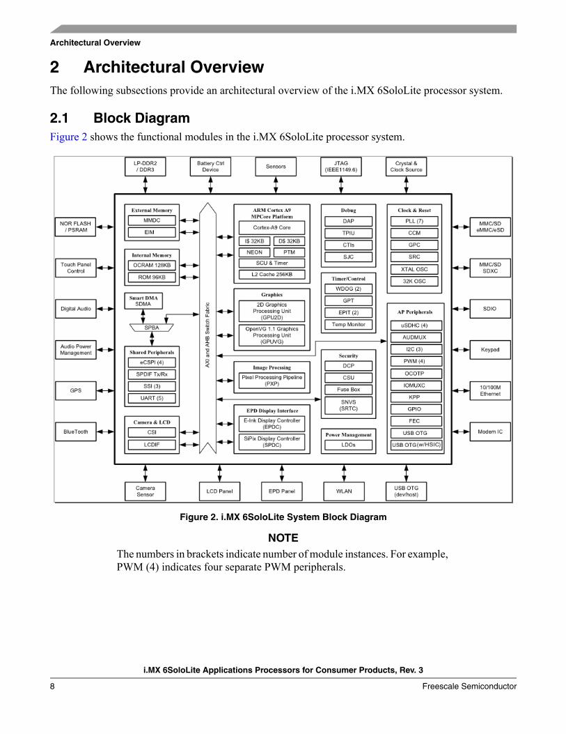
2 Architectural OverviewThe following subsections provide an architectural overview of the i.MX 6SoloLite processor system.
2.1 Block DiagramFigure 2 shows the functional modules in the i.MX 6SoloLite processor system.
Figure 2. i.MX 6SoloLite System Block Diagram
NOTEThe numbers in brackets indicate number of module instances. For example, PWM (4) indicates four separate PWM peripherals.
Modules List
i.MX 6SoloLite Applications Processors for Consumer Products, Rev. 3
Freescale Semiconductor 9
3 Modules ListThe i.MX 6SoloLite processor contains a variety of digital and analog modules. Table 2 describes these modules in alphabetical order.
Table 2. i.MX 6SoloLite Modules List
BlockMnemonic
Block Name Subsystem Brief Description
128x8 Fuse Box
Electrical FuseArray
Security Electrical Fuse Array. Enables to setup Boot Modes, Security Levels, Security Keys, and many other system parameters.The i.MX 6SoloLite processor consists of 2-128x8-bit fuse box accessible through OCOTP_CTRL interface.
ARM ARM Platform ARM The ARM Cortex-A9 platform consists of a Cortex-A9 core version r2p10 and associated sub-blocks, including Level 2 Cache Controller, SCU (Snoop Control Unit), GIC (General Interrupt Controller), private timers, Watchdog, and CoreSight debug modules.
AUDMUX Digital Audio Mux
Multimedia Peripherals
The AUDMUX is a programmable interconnect for voice, audio, and synchronous data routing between host serial interfaces (for example, SSI1, SSI2, and SSI3) and peripheral serial interfaces (audio and voice codecs). The AUDMUX has seven ports with identical functionality and programming models. A desired connectivity is achieved by configuring two or more AUDMUX ports.
CCMGPCSRC
Clock Control Module,
General Power Controller,
System Reset Controller
Clocks, Resets, and Power
Control
These modules are responsible for clock and reset distribution in the system, and also for the system power management.
CSU Central Security Unit
Security The Central Security Unit (CSU) is responsible for setting comprehensive security policy within the i.MX 6SoloLite platform. The Security Control Registers (SCR) of the CSU are set during boot time by the HAB and are locked to prevent further writing.
CTI-1CTI-2CTI-3CTI-4CTI-5
Cross Trigger Interfaces
Debug / Trace Cross Trigger Interfaces allows cross-triggering based on inputs from masters attached to CTIs. The CTI module is internal to the Cortex-A9 Core Platform.
CTM Cross Trigger Matrix
Debug / Trace Cross Trigger Matrix IP is used to route triggering events between CTIs. The CTM module is internal to the Cortex-A9 Core Platform.
DAP Debug Access Port
System Control Peripherals
The DAP provides real-time access for the debugger without halting the core to: • System memory and peripheral registers • All debug configuration registersThe DAP also provides debugger access to JTAG scan chains. The DAP module is internal to the Cortex-A9 Core Platform.
DCP Dataco-processor
Security This module provides support for general encryption and hashing functionstypically used for security functions. Because its basic job is moving datafrom memory to memory, it also incorporates a memory-copy (memcopy)function for both debugging and as a more efficient method of copying databetween memory blocks than the DMA-based approach.
i.MX 6SoloLite Applications Processors for Consumer Products, Rev. 3
10 Freescale Semiconductor
Modules List
eCSPI-1eCSPI-2eCSPI-3eCSPI-4
Configurable SPI
Connectivity Peripherals
Full-duplex enhanced Synchronous Serial Interface. It is configurable to support Master/Slave modes, four chip selects to support multiple peripherals.
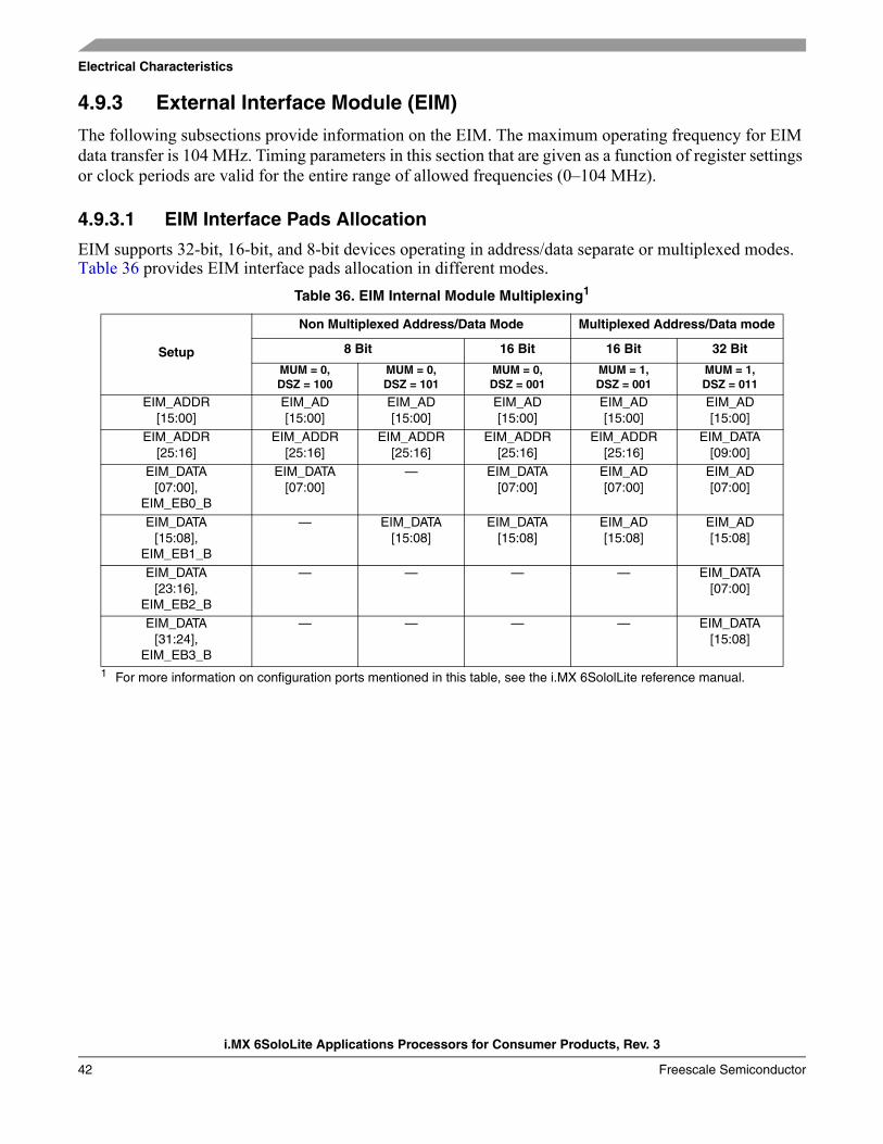
EIM NOR-Flash /PSRAM interface
Connectivity Peripherals
The EIM NOR-FLASH / PSRAM provides: • Support 16-bit (in muxed IO mode only) PSRAM memories (sync and async
operating modes), at slow frequency • Support 16-bit (in muxed IO mode only) NOR-Flash memories, at slow
frequency • Multiple chip selects
EPDC Electrophoretic Display
Controller
Peripherals The EPDC is a feature-rich, low power, and high-performance direct-drive, active matrix EPD controller. It is specifically designed to drive E-INK™ EPD panels, supporting a wide variety of TFT backplanes.
EPIT-1EPIT-2
Enhanced Periodic Interrupt
Timer
Timer Peripherals
Each EPIT is a 32-bit “set and forget” timer that starts counting after the EPIT is enabled by software. It is capable of providing precise interrupts at regular intervals with minimal processor intervention. It has a 12-bit prescaler for division of input clock frequency to get the required time setting for the interrupts to occur, and counter value can be programmed on the fly.
FEC Fast Ethernet Controller
Connectivity Peripherals
The Ethernet Media Access Controller (MAC) is designed to support 10 and 100 Mbps Ethernet/IEEE 802.3 networks. An external transceiver interface and transceiver function are required to complete the interface to the media.
GPIO-1GPIO-2GPIO-3GPIO-4GPIO-5
General Purpose I/O Modules
System Control Peripherals
Used for general purpose input/output to external ICs. Each GPIO module supports 32 bits of I/O.
GPT General Purpose
Timer
Timer Peripherals
Each GPT is a 32-bit “free-running” or “set and forget” mode timer with programmable prescaler and compare and capture register. A timer counter value can be captured using an external event and can be configured to trigger a capture event on either the leading or trailing edges of an input pulse. When the timer is configured to operate in “set and forget” mode, it is capable of providing precise interrupts at regular intervals with minimal processor intervention. The counter has output compare logic to provide the status and interrupt at comparison. This timer can be configured to run either on an external clock or on an internal clock.
GPU2Dv2 Graphics Processing
Unit-2D, ver 2
Multimedia Peripherals
The GPU2Dv2 provides hardware acceleration for 2D graphics algorithms, such as Bit BLT, stretch BLT, and many other 2D functions.
GPUVGv2 Vector Graphics ProcessingUnit, ver2
Multimedia Peripherals
OpenVG graphics accelerator provides OpenVG 1.1 support as well as other accelerations, including Real-time hardware curve tesselation of lines, quadratic and cubic Bezier curves, 16x Line Anti-aliasing, and various Vector Drawing functions.
I2C-1I2C-2I2C-3
I2C Interface Connectivity Peripherals
I2C provide serial interface for external devices. Data rates of up to 400 kbps are supported.
Table 2. i.MX 6SoloLite Modules List (continued)
BlockMnemonic
Block Name Subsystem Brief Description
Modules List
i.MX 6SoloLite Applications Processors for Consumer Products, Rev. 3
Freescale Semiconductor 11
IOMUXC IOMUX Control
System Control Peripherals
This module enables flexible IO multiplexing. Each IO pad has default and several alternate functions. The alternate functions are software configurable.
KPP Key Pad Port Connectivity Peripherals
KPP Supports 8 x 8 external key pad matrix. KPP features are: • Open drain design • Glitch suppression circuit design • Multiple keys detection • Standby key press detection
LCDIF LCD Interface MultimediaPeripherals
The LCDIF provides display data for external LCD panels from simple text-only displays to WVGA, 16/18/24 bpp color TFT panels. The LCDIF supports all of these different interfaces by providing fully programmable functionality and sharing register space, FIFOs, and ALU resources at the same time. The LCDIF supports RGB (DOTCLK) modes as well as system mode including both VSYNC and WSYNC modes.
MMDC Multi-Mode DDR Controller
Connectivity Peripherals
DDR Controller has the following features: • Support 16/32-bit DDR3-800 or LPDDR2-800 • Supports up to 2 GByte DDR memory space
OCOTP_CTRL
OTP Controller
Security The On-Chip OTP controller (OCOTP_CTRL) provides an interface for reading, programming, and/or overriding identification and control information stored in on-chip fuse elements. The module supports electrically-programmable poly fuses (eFUSEs). The OCOTP_CTRL also provides a set of volatile software-accessible signals that can be used for software control of hardware elements, not requiring non-volatility. The OCOTP_CTRL provides the primary user-visible mechanism for interfacing with on-chip fuse elements. Among the uses for the fuses are unique chip identifiers, mask revision numbers, cryptographic keys, JTAG secure mode, boot characteristics, and various control signals, requiring permanent non-volatility.
OCRAM On-Chip Memory Controller
Data Path The On-Chip Memory controller (OCRAM) module is designed as an interface between system’s AXI bus and internal (on-chip) SRAM memory module.In i.MX 6SoloLite processor, the OCRAM is used for controlling the 128 KB multimedia RAM through a 64-bit AXI bus.
OCRAM_L2 On-Chip MemoryController for
L2 Cache
Data Path The On-Chip Memory controller for L2 cache (OCRAM_L2) module is designed as an interface between system’s AXI bus and internal (on-chip) L2 cache memory module during boot mode.
Data Path Integrated power management unit. Used to provide power to various SoC domains.
PWM-1PWM-2PWM-3PWM-4
Pulse Width Modulation
Connectivity Peripherals
The pulse-width modulator (PWM) has a 16-bit counter and is optimized to generate sound from stored sample audio images and it can also generate tones. It uses 16-bit resolution and a 4x16 data FIFO to generate sound.
Table 2. i.MX 6SoloLite Modules List (continued)
BlockMnemonic
Block Name Subsystem Brief Description
i.MX 6SoloLite Applications Processors for Consumer Products, Rev. 3
12 Freescale Semiconductor
Modules List
PXP PiXel Processing
Pipeline
Display Peripherals
A high-performance pixel processor capable of 1 pixel/clock performance for combined operations, such as color-space conversion, alpha blending, gamma-mapping, and rotation. The PXP is enhanced with features specifically for gray scale applications. In addition, the PXP supports traditional pixel/frame processing paths for still-image and video processing applications, allowing it to interface with either of the integrated EPD controllers.
RAM128 KB
Internal RAM Internal Memory
Internal RAM, which is accessed through OCRAM memory controller.
RNGB Random Number Generator
Security Random number generating module.
ROM96KB
Boot ROM Internal Memory
Supports secure and regular Boot Modes. Includes read protection on 4K region for content protection.
ROMCP ROM Controller with Patch
Data Path ROM Controller with ROM Patch support
SDMA Smart Direct Memory Access
System Control Peripherals
The SDMA is multi-channel flexible DMA engine. It helps in maximizing system performance by off-loading the various cores in dynamic data routing. It has the following features: • Powered by a 16-bit Instruction-Set micro-RISC engine • Multi-channel DMA supporting up to 32 time-division multiplexed DMA
channels • 48 events with total flexibility to trigger any combination of channels • Memory accesses including linear, FIFO, and 2D addressing • Shared peripherals between ARM and SDMA • Very fast Context-Software switching with 2-level priority based preemptive
multi-tasking • DMA units with auto-flush and prefetch capability • Flexible address management for DMA transfers (increment, decrement,
and no address changes on source and destination address) • DMA ports can handle unit-directional and bi-directional flows (copy mode) • Up to 8-word buffer for configurable burst transfers • Support of byte-swapping and CRC calculations • Library of Scripts and API is available
SJC System JTAGController
System Control Peripherals
The SJC provides JTAG interface, which complies with JTAG TAP standards, to internal logic. The i.MX 6SoloLite processor uses JTAG port for production, testing, and system debugging. In addition, the SJC provides BSR (Boundary Scan Register) standard support, which complies with IEEE1149.1 and IEEE1149.6 standards. The JTAG port must be accessible during platform initial laboratory bring-up, for manufacturing tests and troubleshooting, as well as for software debugging by authorized entities. The i.MX 6SoloLite SJC incorporates three security modes for protecting against unauthorized accesses. Modes are selected through eFUSE configuration.
SNVS SecureNon-Volatile
Storage
Security Secure Non-Volatile Storage, including Secure Real Time Clock, Security State Machine, Master Key Control, and Violation/Tamper Detection and reporting.
SPDIF Sony Phillips Digital Interface
Multimedia Peripherals
A standard audio file transfer format, developed jointly by the Sony and Phillips corporations. Has Transmitter and Receiver functionality.
Table 2. i.MX 6SoloLite Modules List (continued)
BlockMnemonic
Block Name Subsystem Brief Description
Modules List
i.MX 6SoloLite Applications Processors for Consumer Products, Rev. 3
Freescale Semiconductor 13
SSI-1SSI-2SSI-3
I2S/SSI/AC97 Interface
Connectivity Peripherals
The SSI is a full-duplex synchronous interface, which is used on the AP to provide connectivity with off-chip audio peripherals. The SSI supports a wide variety of protocols (SSI normal, SSI network, I2S, and AC-97), bit depths (up to 24 bits per word), and clock / frame sync options.The SSI has two pairs of 8x24 FIFOs and hardware support for an external DMA controller in order to minimize its impact on system performance. The second pair of FIFOs provides hardware interleaving of a second audio stream that reduces CPU overhead in use cases where two time slots are being used simultaneously.
TEMPMON Temperature Monitor
System Control Peripherals
The temperature monitor/sensor IP, for detecting high temperature conditions. The Temperature sensor IP for detecting die temperature. The temperature read out does not reflect case or ambient temperature, but the proximity of the temperature sensor location on the die. Temperature distribution may not be uniformly distributed, therefore the read out value may not be the reflection of the temperature value of the entire die.
TZASC Trust-Zone Address Space
Controller
Security The TZASC (TZC-380 by ARM) provides security address region control functions required for intended application. It is used on the path to the DRAM controller.
UART-1UART-2UART-3UART-4UART-5
UART Interface
Connectivity Peripherals
Each of the UARTv2 modules support the following serial data transmit/receive protocols and configurations: • 7- or 8-bit data words, 1 or 2 stop bits, programmable parity (even, odd or
none) • Programmable baud rates up to 5 MHz. • 32-byte FIFO on Tx and 32 half-word FIFO on Rx supporting auto-baud • IrDA 1.0 support (up to SIR speed of 115200 bps) • Option to operate as 8-pins full UART, DCE, or DTE
USBOH2A 2x USB 2.0 High Speed OTG and
1x HS Hosts
Connectivity Peripherals
USBO2H contains: • Two high-speed OTG module with integrated HS USB PHY • One identical high-speed Host modules connected to HSIC USB ports.
Table 2. i.MX 6SoloLite Modules List (continued)
BlockMnemonic
Block Name Subsystem Brief Description
i.MX 6SoloLite Applications Processors for Consumer Products, Rev. 3
14 Freescale Semiconductor
Modules List
uSDHC-1uSDHC-2uSDHC-2uSDHC-4
SD/MMC and SDXC
Enhanced Multi-Media Card / Secure Digital Host Controller
Connectivity Peripherals
i.MX 6SoloLite specific SoC characteristics:All four MMC/SD/SDIO controller IPs are identical and are based on the uSDHC IP. They are: • Fully compliant with MMC command/response sets and Physical Layer as
defined in the Multimedia Card System Specification, v4.2/4.3/4.4/4.41 including high-capacity (size > 2 GB) cards HC MMC. HW reset as specified for eMMC cards is supported at ports #3 and #4 only.
• Fully compliant with SD command/response sets and Physical Layer as defined in the SD Memory Card Specifications, v3.0 including high-capacity SDHC cards up to 32 GB and SDXC cards up to 2 TB.
• Fully compliant with SDIO command/response sets and interrupt/read-wait mode as defined in the SDIO Card Specification, Part E1, v1.10
• Fully compliant with SD Card Specification, Part A2, SD Host Controller Standard Specification, v2.00
All four ports support: • 1-bit or 4-bit transfer mode specifications for SD and SDIO cards up to
UHS-I SDR104 mode (104 MB/s max) • 1-bit, 4-bit, or 8-bit transfer mode specifications for MMC cards up to 52
MHz in both SDR and DDR modes (104 MB/s max)However, the SoC level integration and I/O muxing logic restrict the functionality to the following: • Instances #1 and #2 are primarily intended to serve as external slots or
interfaces to on-board SDIO devices. These ports are equipped with “Card detection” and “Write Protection” pads and do not support HW reset.
• All ports can work with 1.8 V and 3.3 V cards. There are two completely independent I/O power domains for Ports #1 and #2 in four bit configuration (SD interface). Port #3 is placed in his own independent power domain and port #4 shares power domain with some other interfaces.
WDOG-1 Watchdog Timer Peripherals
The Watchdog Timer supports two comparison points during each counting period. Each of the comparison points is configurable to evoke an interrupt to the ARM core, and a second point evokes an external event on the WDOG line.
WDOG-2(TZ)
Watchdog (TrustZone)
Timer Peripherals
The TrustZone Watchdog (TZ WDOG) timer module protects against TrustZone starvation by providing a method of escaping normal mode and forcing a switch to the TZ mode. TZ starvation is a situation where the normal OS prevents switching to the TZ mode. Such situation is undesirable as it can compromise the system’s security. Once the TZ WDOG module is activated, it must be serviced by TZ software on a periodic basis. If servicing does not take place, the timer times out. Upon a time-out, the TZ WDOG asserts a TZ mapped interrupt that forces switching to the TZ mode. If it is still not served, the TZ WDOG asserts a security violation signal to the CSU. The TZ WDOG module cannot be programmed or deactivated by a normal mode Software.
XTALOSC Crystal Oscillator I/F
Clocking The XTALOSC module enables connectivity to external crystal oscillator device. In a typical application use-case, it is used for 24 MHz oscillator.
Table 2. i.MX 6SoloLite Modules List (continued)
BlockMnemonic
Block Name Subsystem Brief Description
Modules List
i.MX 6SoloLite Applications Processors for Consumer Products, Rev. 3
Freescale Semiconductor 15
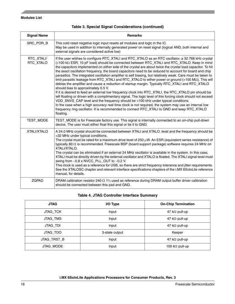
3.1 Special Signal ConsiderationsTable 3 lists special signal considerations for the i.MX 6SoloLite processor. The signal names are listed in alphabetical order.
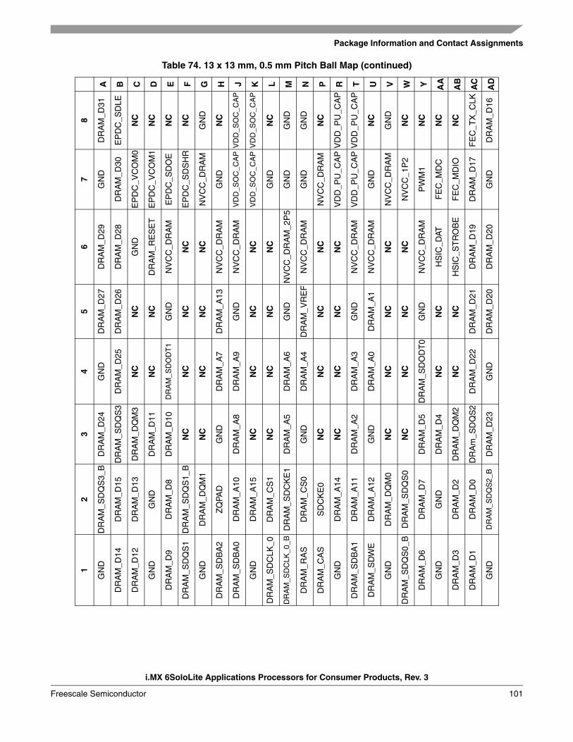
The package contact assignments can be found in Section 6, “Package Information and Contact Assignments.” Signal descriptions are provided in the i.MX 6SoloLite reference manual.
Table 3. Special Signal Considerations
Signal Name Remarks
XTALOSC_CLK1_P/XTALOSC_CLK1_N
One general purpose differential high speed clock Input/output is provided.It could be used to: • To feed external reference clock to the PLLs and further to the modules inside SoC, for example as
alternate reference clock for Audio interfaces, etc. • To output internal SoC clock to be used outside the SoC as either reference clock or as a functional
clock for peripherals. See the i.MX 6SoloLite reference manual for details on the respective clock trees.The clock inputs/outputs are LVDS differential pairs compatible with TIA/EIA-644 standard, the maximum clock out frequency range supported is 528 MHz.Alternatively one may use single ended signal to drive XTALOSC_CLK1_P input. In this case, the corresponding XTALOSC_CLK1_N input should be tied to the constant voltage level equal 1/2 of the input signal swing.Termination should be provided in case of high frequency signals.See LVDS pad electrical specification for further details.After initialization, the XTALOSC_CLK1 input/output could be disabled (if not used). If unused, the XTALOSC_CLK1_N/P pair may be left floating.
DRAM_VREF When using DRAM_VREF with DDR I/O, the nominal reference voltage must be half of the NVCC_DRAM supply. The user must tie DRAM_VREF to a precision external resistor divider. Use a 1 k 0.5% resistor to GND and a 1 k 0.5% resistor to NVCC_DRAM. Shunt each resistor with a closely-mounted 0.1 µF capacitor.To reduce supply current, a pair of 1.5 k 0.1% resistors can be used. Using resistors with recommended tolerances ensures the ± 2% DRAM_VREF tolerance (per the DDR3 specification) is maintained when four DDR3 ICs plus the i.MX 6SoloLite are drawing current on the resistor divider.It is recommended to use regulated power supply for “big” memory configurations (more that eight devices).
JTAG_nnnn The JTAG interface is summarized in Table 4. Use of external resistors is unnecessary. However, if external resistors are used, the user must ensure that the on-chip pull-up/down configuration is followed. For example, do not use an external pull down on an input that has on-chip pull-up.
JTAG_TDO is configured with a keeper circuit such that the floating condition is eliminated if an external pull resistor is not present. An external pull resistor on JTAG_TDO is detrimental and should be avoided.
JTAG_MODE must be externally connected to GND for normal operation. Termination to GND through an external pull-down resistor (such as 1 k) is allowed. JTAG_MODE set to high configures the JTAG interface to mode compliant with IEEE1149.1 standard. JTAG_MODE set to low configures the JTAG interface for common Software debug adding all the system TAPs to the chain.
NC These signals are No Connect (NC) and should be floated by the user.
SRC_ONOFF In normal mode may be connected to ONOFF button (de-bouncing provided at this input). Internally this pad is pulled up. A short duration (<5s) connection to GND in OFF mode causes the internal power management state machine to change the state to ON. In ON mode, a short duration connection to GND generates interrupt (intended to initiate a software controllable power down). A long duration (above ~5s) connection to GND causes “forced” OFF.
i.MX 6SoloLite Applications Processors for Consumer Products, Rev. 3
16 Freescale Semiconductor
Modules List
SRC_POR_B This cold reset negative logic input resets all modules and logic in the IC.May be used in addition to internally generated power on reset signal (logical AND, both internal and external signals are considered active low)
RTC_XTALI/RTC_XTALO
If the user wishes to configure RTC_XTALI and RTC_XTALO as an RTC oscillator, a 32.768 kHz crystal (100 k ESR, 10 pF load) should be connected between RTC_XTALI and RTC_XTALO. Keep in mind the capacitors implemented on either side of the crystal are about twice the crystal load capacitor. To hit the exact oscillation frequency, the board capacitors need to be reduced to account for board and chip parasitics. The integrated oscillation amplifier is self biasing, but relatively weak. Care must be taken to limit parasitic leakage from RTC_XTALI and RTC_XTALO to either power or ground (>100 M). This will debias the amplifier and cause a reduction of startup margin. Typically RTC_XTALI and RTC_XTALO should bias to approximately 0.5 V.If it is desired to feed an external low frequency clock into RTC_XTALI, the RTC_XTALO pin should be left floating or driven with a complimentary signal. The logic level of this forcing clock should not exceed VDD_SNVS_CAP level and the frequency should be <100 kHz under typical conditions.In the case when a high accuracy real time clock is not required, the system may use an internal low frequency ring oscillator. It is recommended to connect RTC_XTALI to GND and keep RTC_XTALO floating.
TEST_MODE TEST_MODE is for Freescale factory use. This signal is internally connected to an on-chip pull-down device. The user must either float this signal or tie it to GND.
XTALI/XTALO A 24.0 MHz crystal should be connected between XTALI and XTALO. level and the frequency should be <32 MHz under typical conditions.The crystal must be rated for a maximum drive level of 250 W. An ESR (equivalent series resistance) of typically 80 is recommended. Freescale BSP (board support package) software requires 24 MHz on XTALI/XTALO.The crystal can be eliminated if an external 24 MHz oscillator is available in the system. In this case, XTALI must be directly driven by the external oscillator and XTALO is floated. The XTALI signal level must swing from ~0.8 x NVCC_PLL_OUT to ~0.2 V. This clock is used as a reference for USB, so there are strict frequency tolerance and jitter requirements. See the XTALOSC chapter and relevant interface specifications chapters of the i.MX 6SoloLite reference manual, for details.
ZQPAD DRAM calibration resistor 240 1% used as reference during DRAM output buffer driver calibration should be connected between this pad and GND.
Table 4. JTAG Controller Interface Summary
JTAG I/O Type On-Chip Termination
JTAG_TCK Input 47 kpull-up
JTAG_TMS Input 47 kpull-up
JTAG_TDI Input 47 kpull-up
JTAG_TDO 3-state output Keeper
JTAG_TRST_B Input 47 kpull-up
JTAG_MODE Input 100 kpull-up
Table 3. Special Signal Considerations (continued)
Signal Name Remarks
Electrical Characteristics
i.MX 6SoloLite Applications Processors for Consumer Products, Rev. 3
Freescale Semiconductor 17
3.2 Recommended Connections for Unused Analog InterfacesTable 5 shows the recommended connections for unused analog interfaces.
4 Electrical CharacteristicsThis section provides the device and module-level electrical characteristics for the i.MX 6SoloLite.
4.1 Chip-Level ConditionsThis section provides the device-level electrical characteristics for the IC. See Table 6 for a quick reference to the individual tables and sections.
4.1.1 Absolute Maximum Ratings
CAUTIONStresses beyond those listed under Table 7 may affect reliability or cause permanent damage to the device. These are stress ratings only. Functional operation of the device at these or any other conditions beyond those indicated in the Operating Ranges or Parameters tables is not implied.
Table 5. Recommended Connections for Unused Analog Interfaces
Module Pad Name Recommendations if Unused?
XTALOSC XTALOSC_CLK1_N, XTALOSC_CLK1_P Float
USB USB_OTGx_DN, USB_OTGx_DP, USB_OTGx_VBUS, USB_OTG_CHD_B Float
Table 6. i.MX 6SoloLite Chip-Level Conditions
For these characteristics, … Topic appears …
Absolute Maximum Ratings on page 18
BGA Case 2240 Package Thermal Resistance on page 18
Operating Ranges on page 20
External Clock Sources on page 22
Maximum Supply Currents on page 23
Low Power Mode Supply Currents on page 24
USB PHY Current Consumption on page 25
i.MX 6SoloLite Applications Processors for Consumer Products, Rev. 3
18 Freescale Semiconductor
Electrical Characteristics
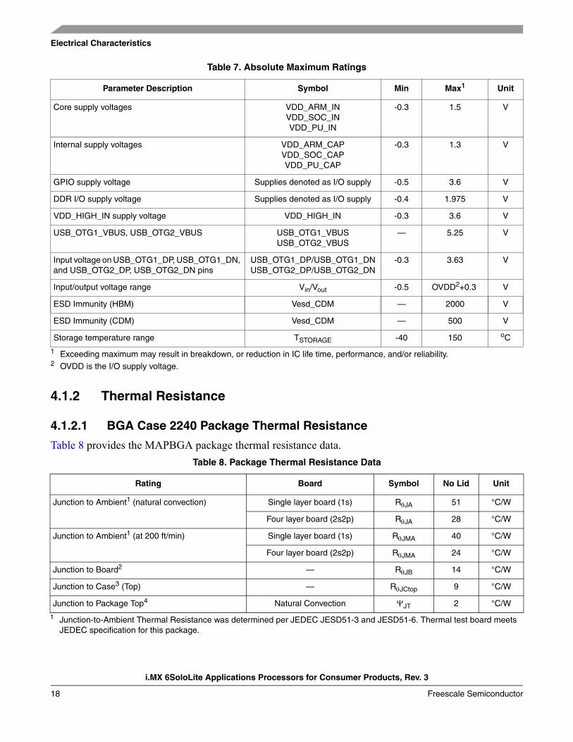
4.1.2 Thermal Resistance
4.1.2.1 BGA Case 2240 Package Thermal Resistance
Table 8 provides the MAPBGA package thermal resistance data.
Table 7. Absolute Maximum Ratings
Parameter Description Symbol Min Max1
1 Exceeding maximum may result in breakdown, or reduction in IC life time, performance, and/or reliability.
Input voltage on USB_OTG1_DP, USB_OTG1_DN, and USB_OTG2_DP, USB_OTG2_DN pins
USB_OTG1_DP/USB_OTG1_DNUSB_OTG2_DP/USB_OTG2_DN
-0.3 3.63 V
Input/output voltage range Vin/Vout -0.5 OVDD2+0.3
2 OVDD is the I/O supply voltage.
V
ESD Immunity (HBM) Vesd_CDM — 2000 V
ESD Immunity (CDM) Vesd_CDM — 500 V
Storage temperature range TSTORAGE -40 150 oC
Table 8. Package Thermal Resistance Data
Rating Board Symbol No Lid Unit
Junction to Ambient1 (natural convection)
1 Junction-to-Ambient Thermal Resistance was determined per JEDEC JESD51-3 and JESD51-6. Thermal test board meets JEDEC specification for this package.
Single layer board (1s) RJA 51 °C/W
Four layer board (2s2p) RJA 28 °C/W
Junction to Ambient1 (at 200 ft/min) Single layer board (1s) RJMA 40 °C/W
Four layer board (2s2p) RJMA 24 °C/W
Junction to Board2 — RJB 14 °C/W
Junction to Case3 (Top) — RJCtop 9 °C/W
Junction to Package Top4 Natural Convection JT 2 °C/W
Electrical Characteristics
i.MX 6SoloLite Applications Processors for Consumer Products, Rev. 3
Freescale Semiconductor 19
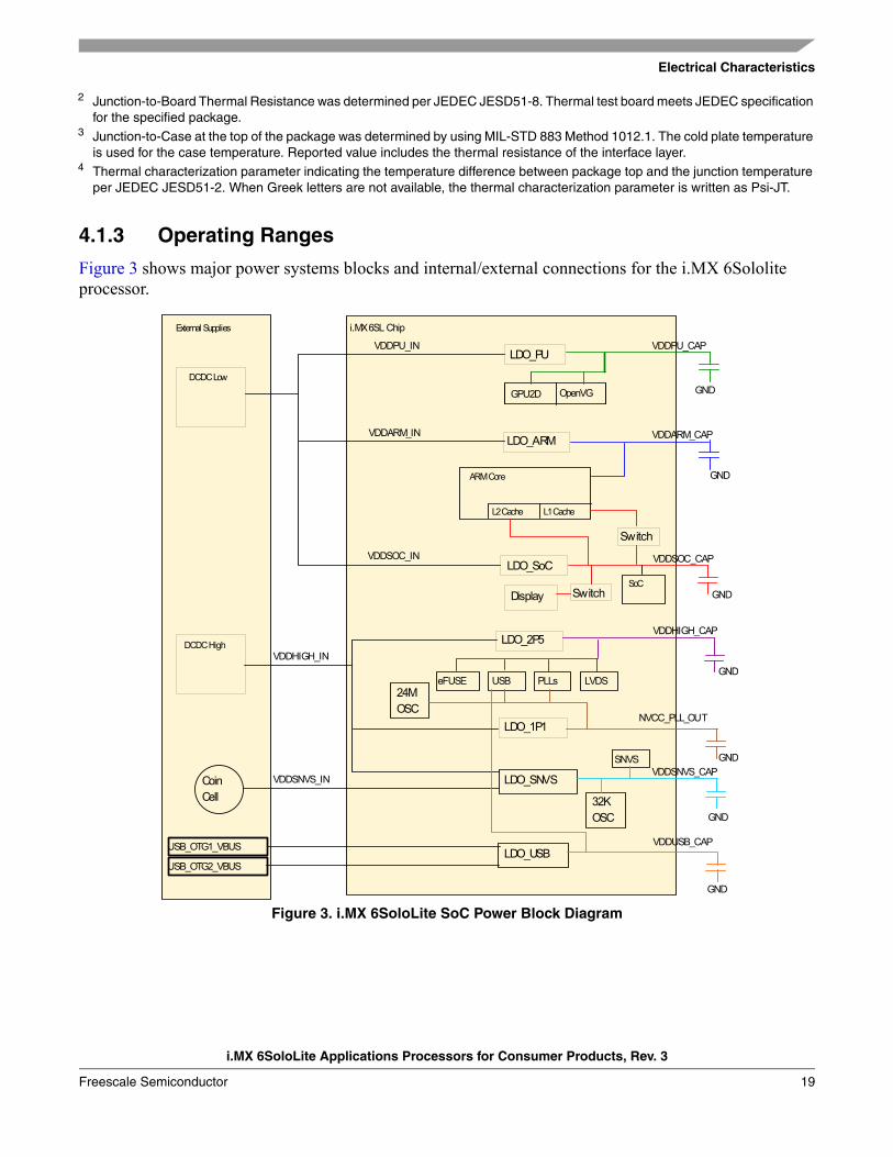
4.1.3 Operating Ranges
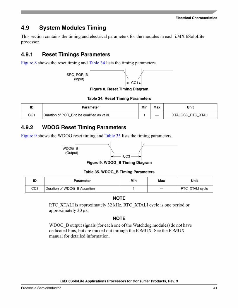
Figure 3 shows major power systems blocks and internal/external connections for the i.MX 6Sololite processor.
Figure 3. i.MX 6SoloLite SoC Power Block Diagram
2 Junction-to-Board Thermal Resistance was determined per JEDEC JESD51-8. Thermal test board meets JEDEC specification for the specified package.
3 Junction-to-Case at the top of the package was determined by using MIL-STD 883 Method 1012.1. The cold plate temperature is used for the case temperature. Reported value includes the thermal resistance of the interface layer.
4 Thermal characterization parameter indicating the temperature difference between package top and the junction temperature per JEDEC JESD51-2. When Greek letters are not available, the thermal characterization parameter is written as Psi-JT.
External Supplies
DCDC Low
LDO_PU
GPU2D OpenVG
LDO_ARM
L1 Cache
ARM Core
LDO_SoC
SoC
LDO_2P5
eFUSE USB PLLs LVDS
LDO_1P1
24MOSC
LDO_SNVS
SNVS
32KOSC
LDO_USB
DCDC High
Coin Cell
USB_OTG2_VBUS
VDDPU_CAP
i.MX 6SL Chip
VDDPU_IN
VDDARM_IN
GND
GND
GND
GND
GND
GND
GND
VDDARM_CAP
VDDSOC_CAP
VDDHIGH_CAP
NVCC_PLL_OUT
VDDSNVS_CAP
VDDUSB_CAP
VDDSNVS_IN
VDDHIGH_IN
VDDSOC_IN
USB_OTG1_VBUS
L2 Cache
SwitchDisplay
Switch
i.MX 6SoloLite Applications Processors for Consumer Products, Rev. 3
20 Freescale Semiconductor
Electrical Characteristics
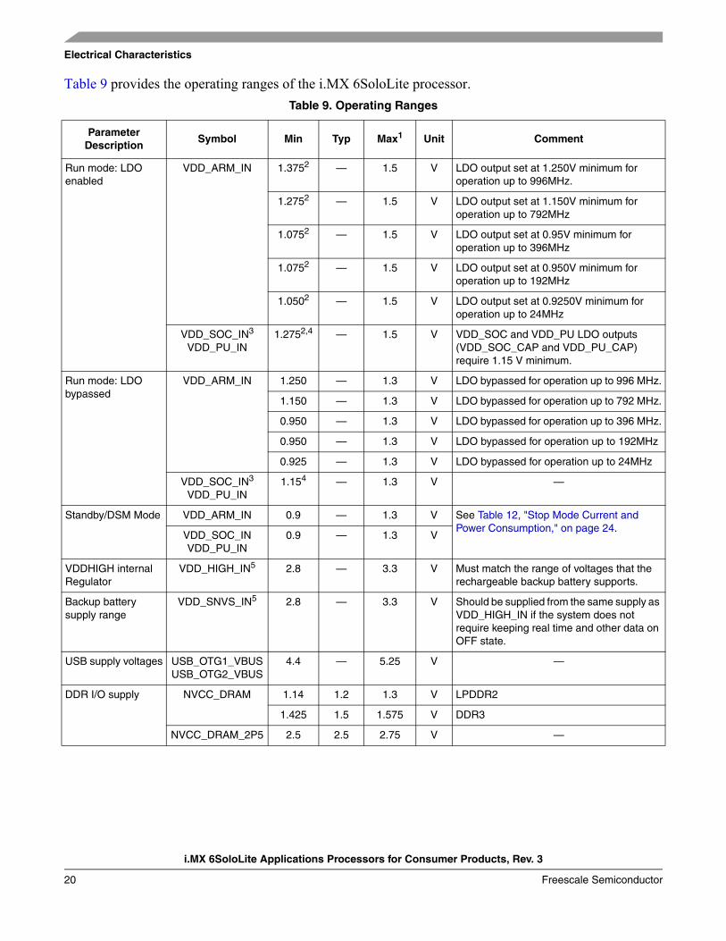
Table 9 provides the operating ranges of the i.MX 6SoloLite processor.
Table 9. Operating Ranges
Parameter Description
Symbol Min Typ Max1 Unit Comment
Run mode: LDO enabled
VDD_ARM_IN 1.3752 — 1.5 V LDO output set at 1.250V minimum for operation up to 996MHz.
1.2752 — 1.5 V LDO output set at 1.150V minimum for operation up to 792MHz
1.0752 — 1.5 V LDO output set at 0.95V minimum for operation up to 396MHz
1.0752 — 1.5 V LDO output set at 0.950V minimum for operation up to 192MHz
1.0502 — 1.5 V LDO output set at 0.9250V minimum for operation up to 24MHz
VDD_SOC_IN3
VDD_PU_IN1.2752,4 — 1.5 V VDD_SOC and VDD_PU LDO outputs
(VDD_SOC_CAP and VDD_PU_CAP) require 1.15 V minimum.
Run mode: LDO bypassed
VDD_ARM_IN 1.250 — 1.3 V LDO bypassed for operation up to 996 MHz.
1.150 — 1.3 V LDO bypassed for operation up to 792 MHz.
0.950 — 1.3 V LDO bypassed for operation up to 396 MHz.
0.950 — 1.3 V LDO bypassed for operation up to 192MHz
0.925 — 1.3 V LDO bypassed for operation up to 24MHz
VDD_SOC_IN3
VDD_PU_IN1.154 — 1.3 V —
Standby/DSM Mode VDD_ARM_IN 0.9 — 1.3 V See Table 12, "Stop Mode Current and Power Consumption," on page 24.
VDD_SOC_IN VDD_PU_IN
0.9 — 1.3 V
VDDHIGH internal Regulator
VDD_HIGH_IN5 2.8 — 3.3 V Must match the range of voltages that the rechargeable backup battery supports.
Backup battery supply range
VDD_SNVS_IN5 2.8 — 3.3 V Should be supplied from the same supply as VDD_HIGH_IN if the system does not require keeping real time and other data on OFF state.
USB supply voltages USB_OTG1_VBUSUSB_OTG2_VBUS
4.4 — 5.25 V —
DDR I/O supply NVCC_DRAM 1.14 1.2 1.3 V LPDDR2
1.425 1.5 1.575 V DDR3
NVCC_DRAM_2P5 2.5 2.5 2.75 V —
Electrical Characteristics
i.MX 6SoloLite Applications Processors for Consumer Products, Rev. 3
Freescale Semiconductor 21
4.1.4 External Clock Sources
Each i.MX 6SoloLite processor has two external input system clocks: a low frequency (RTC_XTALI) and a high frequency (XTALI).
The RTC_XTALI is used for low-frequency functions. It supplies the clock for wake-up circuit, power-down real time clock operation, and slow system and watchdog counters. The clock input can be connected to either an external oscillator or a crystal using the internal oscillator amplifier. Additionally, there is an internal ring oscillator, which can substitute the RTC_XTALI, in case accuracy is not important.
The system clock input XTALI is used to generate the main system clock. It supplies the PLLs and other peripherals. The system clock input can be connected to either an external oscillator or a crystal using the internal oscillator amplifier.
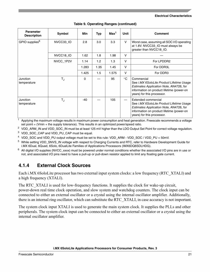
GPIO supplies6 NVCC33_IO 2.8 3.0 3.3 V Worst case, assuming all SOC I/O operating at 1.8V. NVCC33_IO must always be greater than NVCC18_IO.
NVCC18_IO 1.62 1.8 1.98 V —
NVCC_1P2V 1.14 1.2 1.3 V For LPDDR2
1.283 1.35 1.45 V For DDR3L
1.425 1.5 1.575 V For DDR3
Junction temperature
TJ 0 — 95 C CommercialSee i.MX 6SoloLite Product Lifetime Usage Estimates Application Note, AN4726, for information on product lifetime (power-on years) for this processor.
Junction temperature
TJ -40 — 105 — Extended commercialSee i.MX 6SoloLite Product Lifetime Usage Estimates Application Note, AN4726, for information on product lifetime (power-on years) for this processor.
1 Applying the maximum voltage results in maximum power consumption and heat generation. Freescale recommends a voltage set point = (Vmin + the supply tolerance). This results in an optimized power/speed ratio.
2 VDD_ARM_IN and VDD_SOC_IN must be at least 125 mV higher than the LDO Output Set Point for correct voltage regulation.3 VDD_SOC_CAP and VDD_PU_CAP must be equal.4 VDD_SOC and VDD_PU output voltage must be set to this rule: VDD_ARM - VDD_SOC / VDD_PU < 50mV.5 While setting VDD_SNVS_IN voltage with respect to Charging Currents and RTC, refer to Hardware Development Guide for
i.MX 6Dual, 6Quad, 6Solo, 6DualLite Families of Applications Processors (IMX6DQ6SDLHDG).6 All digital I/O supplies (NVCC_xxxx) must be powered under normal conditions whether the associated I/O pins are in use or
not, and associated I/O pins need to have a pull-up or pull-down resistor applied to limit any floating gate current.
Table 9. Operating Ranges (continued)
Parameter Description
Symbol Min Typ Max1 Unit Comment
i.MX 6SoloLite Applications Processors for Consumer Products, Rev. 3
22 Freescale Semiconductor
Electrical Characteristics
NOTEThe internal RTC oscillator does not provide an accurate frequency and is affected by process, voltage, and temperature variations. Freescale strongly recommends using an external crystal as the RTC_XTALI reference. If the internal oscillator is used instead, careful consideration must be given to the timing implications on all of the SoC modules dependent on this clock.
Table 10 shows the interface frequency requirements.
The typical values shown in Table 10 are required for use with Freescale BSPs to ensure precise time keeping and USB operation. For RTC_XTALI operation, two clock sources are available:
• On-chip 40 kHz ring oscillator: This clock source has the following characteristics:
— Approximately 25 A more Idd than crystal oscillator
— Approximately ±50% tolerance
— No external component required
— Starts up quicker than 32 kHz crystal oscillator
• External crystal oscillator with on-chip support circuit
— At power up, ring oscillator is utilized. After crystal oscillator is stable, the clock circuit switches over to the crystal oscillator automatically.
— Higher accuracy than ring oscillator
— If no external crystal is present, then the ring oscillator is utilized
The decision to choose a clock source should be taken based on real-time clock use and precision time-out.
4.1.5 Maximum Supply Currents
The Power Virus numbers shown in Table 11 represent a use case designed specifically to show the maximum current consumption possible. All cores are running at the defined maximum frequency and are limited to L1 cache accesses only to ensure no pipeline stalls. Although a valid condition, it would have a very limited practical use case, if at all, and be limited to an extremely low duty cycle unless the intention was to specifically show the worst case power consumption.
Table 10. External Input Clock Frequency
Parameter Description Symbol Min Typ Max Unit
RTC_XTALI Oscillator1, 2
1 External oscillator or a crystal with internal oscillator amplifier.2 The required frequency stability of this clock source is application dependent. For recommendations, see Hardware
Development Guide for i.MX 6Dual, 6Quad, 6Solo, 6DualLite Families of Applications Processors (IMX6DQ6SDLHDG).
fckil — 32.768(see 3)/32.0
3 Recommended nominal frequency 32.768 kHz.
— kHz
XTALI Oscillator4, 2
4 External oscillator or a fundamental frequency crystal with internal oscillator amplifier.
fxtal — 24 — MHz
Electrical Characteristics
i.MX 6SoloLite Applications Processors for Consumer Products, Rev. 3
Freescale Semiconductor 23
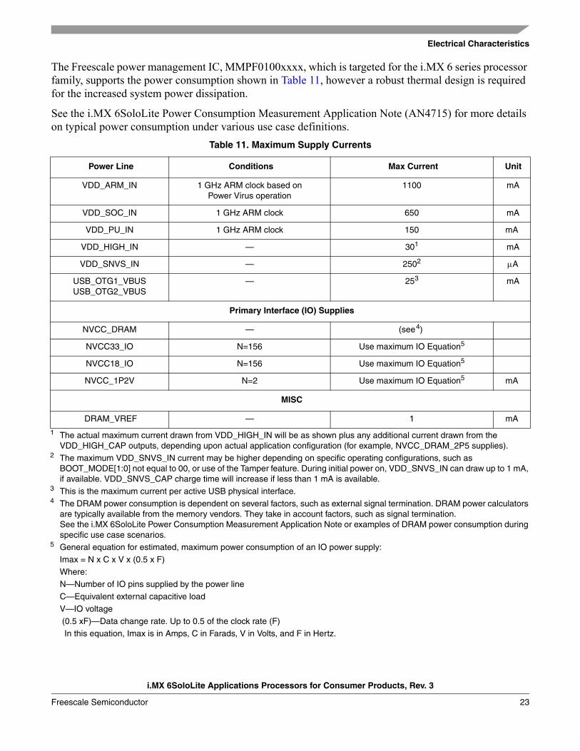
The Freescale power management IC, MMPF0100xxxx, which is targeted for the i.MX 6 series processor family, supports the power consumption shown in Table 11, however a robust thermal design is required for the increased system power dissipation.
See the i.MX 6SoloLite Power Consumption Measurement Application Note (AN4715) for more details on typical power consumption under various use case definitions.
Table 11. Maximum Supply Currents
Power Line Conditions Max Current Unit
VDD_ARM_IN 1 GHz ARM clock based onPower Virus operation
1100 mA
VDD_SOC_IN 1 GHz ARM clock 650 mA
VDD_PU_IN 1 GHz ARM clock 150 mA
VDD_HIGH_IN — 301
1 The actual maximum current drawn from VDD_HIGH_IN will be as shown plus any additional current drawn from the VDD_HIGH_CAP outputs, depending upon actual application configuration (for example, NVCC_DRAM_2P5 supplies).
mA
VDD_SNVS_IN — 2502
2 The maximum VDD_SNVS_IN current may be higher depending on specific operating configurations, such as BOOT_MODE[1:0] not equal to 00, or use of the Tamper feature. During initial power on, VDD_SNVS_IN can draw up to 1 mA, if available. VDD_SNVS_CAP charge time will increase if less than 1 mA is available.
A
USB_OTG1_VBUS USB_OTG2_VBUS
— 253
3 This is the maximum current per active USB physical interface.
mA
Primary Interface (IO) Supplies
NVCC_DRAM — (see4)
4 The DRAM power consumption is dependent on several factors, such as external signal termination. DRAM power calculators are typically available from the memory vendors. They take in account factors, such as signal termination.See the i.MX 6SoloLite Power Consumption Measurement Application Note or examples of DRAM power consumption during specific use case scenarios.
NVCC33_IO N=156 Use maximum IO Equation5
5 General equation for estimated, maximum power consumption of an IO power supply:
Imax = N x C x V x (0.5 x F)
Where:N—Number of IO pins supplied by the power line
C—Equivalent external capacitive load
V—IO voltage
(0.5 xF)—Data change rate. Up to 0.5 of the clock rate (F) In this equation, Imax is in Amps, C in Farads, V in Volts, and F in Hertz.
NVCC18_IO N=156 Use maximum IO Equation5
NVCC_1P2V N=2 Use maximum IO Equation5 mA
MISC
DRAM_VREF — 1 mA
i.MX 6SoloLite Applications Processors for Consumer Products, Rev. 3
24 Freescale Semiconductor
Electrical Characteristics
4.1.6 Low Power Mode Supply CurrentsTable 12 shows the current core consumption (not including I/O) of i.MX 6SoloLite processor in selected low power modes.
Table 12. Stop Mode Current and Power Consumption
Mode Test Conditions Supply Typical1
1 The typical values shown here are for information only and are not guaranteed. These values are average values measured on a worst-case wafer at 25C.
Unit
WAIT • ARM, SoC, and PU LDOs are set to 1.225 V • HIGH LDO set to 2.5 V • Clocks are gated • DDR is in self refresh • PLLs are active in bypass (24 MHz) • Supply voltages remain ON
VDD_ARM_IN (1.375 V) 4 mA
VDD_SOC_IN (1.375 V) 7.5
VDD_PU_IN (1.375 V) 1.5
VDD_HIGH_IN(3.0 V) 9
Total 44.9 mW
STOP_ON • ARM LDO set to 0.9 V • SoC and PU LDOs set to 1.225 V • HIGH LDO set to 2.5 V • PLLs disabled • DDR is in self refresh
VDD_ARM_IN (1.375 V) 2.5 mA
VDD_SOC_IN (1.375 V) 7.5
VDD_PU_IN (1.375 V) 1.5
VDD_HIGH_IN (3.0 V) 4.5
Total 29.3 mW
STOP_OFF • ARM LDO set to 0.9 V • SoC LDO set to 1.225 V • PU LDO is power gated • HIGH LDO set to 2.5 V • PLLs disabled • DDR is in self refresh
VDD_ARM_IN (1.375 V) 2.5 mA
VDD_SOC_IN (1.375 V) 7.5
VDD_PU_IN (1.375 V) 0.1
VDD_HIGH_IN (3.0 V) 4.0
Total 25.9 mW
STANDBY • ARM and PU LDOs are power gated • SoC LDO is in bypass • HIGH LDO is set to 2.5 V • PLLs are disabled • Low voltage • Well Bias ON • XTAL is enabled
VDD_ARM_IN (0.9 V) 0.1 mA
VDD_SoC_IN (0.9 V) 1.0
VDD_PU_IN (0.9 V) 0.1
VDD_HIGH_IN (3.0 V) 3
Total 10.1 mW
Deep Sleep Mode(DSM)
• ARM and PU LDOs are power gated • SoC LDO is in bypass • HIGH LDO is set to 2.5 V • PLLs are disabled • Low voltage • Well Bias ON • XTAL and bandgap are disabled
VDD_ARM_IN (0.9 V) 0.1 mA
VDD_SoC_IN (0.9 V) 0.75
VDD_PU_IN (0.9 V) 0.1
VDD_HIGH_IN (3.0 V) 0.15
Total 1.3 mW
SNVS Only • VDD_SNVS_IN powered • All other supplies off • SRTC running
VDD_SNVS_IN (2.8V) 41 A
Total 115 W
Electrical Characteristics
i.MX 6SoloLite Applications Processors for Consumer Products, Rev. 3
Freescale Semiconductor 25
4.1.7 USB PHY Current Consumption
4.1.7.1 Power Down Mode
In power down mode, everything is powered down, including the USB_OTGx_VBUS valid detectors, typical condition. Table 13 shows the USB interface current consumption in power down mode.
NOTEThe currents on the VDD_HIGH_CAP and VDD_USB_CAP were identified to be the voltage divider circuits in the USB-specific level shifters.
4.2 Power Supplies Requirements and RestrictionsThe system design must comply with power-up sequence, power-down sequence, and steady state guidelines as described in this section to guarantee the reliable operation of the device. Any deviation from these sequences may result in the following situations:
• Excessive current during power-up phase
• Prevention of the device from booting
• Irreversible damage to the processor (worst-case scenario)
4.2.1 Power-Up SequenceFor power-up sequence, the restrictions are as follows:
• VDD_SNVS_IN supply must be turned ON before any other power supply. It may be connected (shorted) with VDD_HIGH_IN supply.
• If a coin cell is used to power VDD_SNVS_IN, then ensure that it is connected before any other supply is switched on.
• If the external SRC_POR_B signal is used to control the processor POR, then SRC_POR_B must be immediately asserted at power-up and remain asserted until the VDD_ARM_CAP, VDD_SOC_CAP, and VDD_PU_CAP supplies are stable. VDD_ARM_IN and VDD_SOC_IN may be applied in either order with no restrictions. In the absence of an external reset feeding the SRC_POR_B input, the internal POR module takes control. See the i.MX 6SoloLite reference manual (IMX6SLRM) for further details and to ensure that all necessary requirements are being met.
• If the external SRC_POR_B signal is not used (always held high or left unconnected), the processor defaults to the internal POR function (where the PMU controls generation of the POR based on the power supplies). If the internal POR function is used, the following power supply requirements must be met:
— VDD_ARM_IN and VDD_SOC_IN may be supplied from the same source, or
Table 13. USB PHY Current Consumption in Power Down Mode
i.MX 6SoloLite Applications Processors for Consumer Products, Rev. 3
26 Freescale Semiconductor
Electrical Characteristics
— VDD_SOC_IN can be supplied before VDD_ARM_IN with a maximum delay of 1 ms.
NOTEEnsure that there is no back voltage (leakage) from any supply on the board towards the 3.3 V supply (for example, from the external components that use both the 1.8 V and 3.3 V supplies).
NOTEUSB_OTG_VBUS and USB_H1_VBUS are not part of the power supply sequence and can be powered at any time.
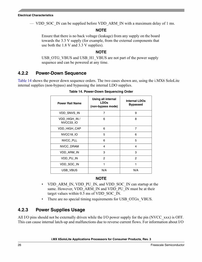
4.2.2 Power-Down Sequence
Table 14 shows the power down sequence orders. The two cases shown are, using the i.MX6 SoloLite internal supplies (non-bypass) and bypassing the internal LDO supplies.
NOTE• VDD_ARM_IN, VDD_PU_IN, and VDD_SOC_IN can startup at the
same. However, VDD_ARM_IN and VDD_PU_IN must be at their target values within 0.5 ms of VDD_SOC_IN.
• There are no special timing requirements for USB_OTGx_VBUS.
4.2.3 Power Supplies Usage
All I/O pins should not be externally driven while the I/O power supply for the pin (NVCC_xxx) is OFF. This can cause internal latch-up and malfunctions due to reverse current flows. For information about I/O
Table 14. Power-Down Sequencing Order
Power Rail NameUsing all internal
LDOs (non-bypass mode)
Internal LDOs Bypassed
VDD_SNVS_IN 7 9
VDD_HIGH_IN / NVCC33_IO
6 8
VDD_HIGH_CAP 6 7
NVCC18_IO 5 6
NVCC_PLL 6 5
NVCC_DRAM 4 4
VDD_ARM_IN 3 3
VDD_PU_IN 2 2
VDD_SOC_IN 1 1
USB_VBUS N/A N/A
Electrical Characteristics
i.MX 6SoloLite Applications Processors for Consumer Products, Rev. 3
Freescale Semiconductor 27
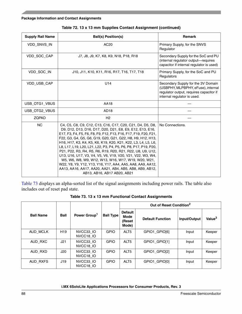
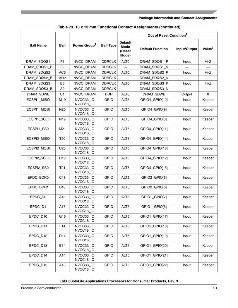
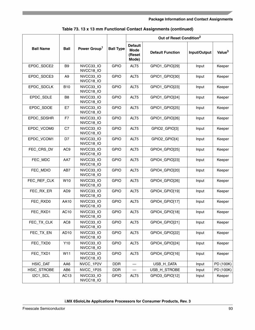
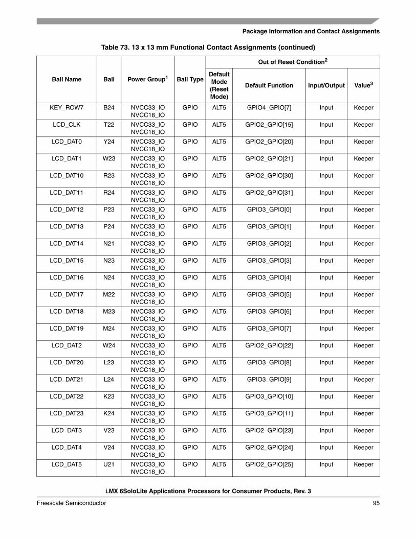
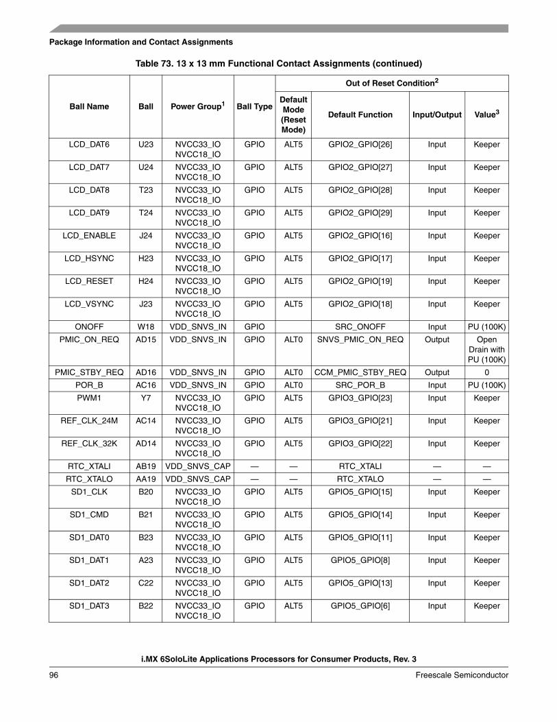
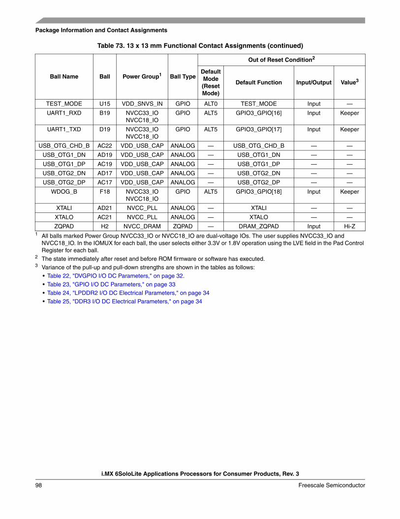
power supply of each pin, see “Power Group” column of Table 73, "13 x 13 mm Functional Contact Assignments," on page 88.
4.3 Integrated LDO Voltage Regulator ParametersVarious internal supplies can be powered ON from internal LDO voltage regulators. All the supply pins named *_CAP must be connected to external capacitors. The onboard LDOs are intended for internal use only and should not be used to power any external circuitry. See the i.MX 6SoloLite reference manual for details on the power tree scheme recommended operation.
NOTEThe *_CAP signals should not be powered externally. These signals are intended for internal LDO or LDO bypass operation only.
4.3.1 Digital Regulators (LDO_ARM, LDO_PU, LDO_SOC)
There are three digital LDO regulators (“Digital”, because of the logic loads that they drive, not because of their construction). The advantages of the regulators are to reduce the input supply variation because of their input supply ripple rejection and their on die trimming. This translates into more voltage for the die producing higher operating frequencies. These regulators have three basic modes.
• Bypass. The regulation FET is switched fully on passing the external voltage, DCDC_LOW, to the load unaltered. The analog part of the regulator is powered down in this state, removing any loss other than the IR drop through the power grid and FET.
• Power Gate. The regulation FET is switched fully off limiting the current draw from the supply. The analog part of the regulator is powered down here limiting the power consumption.
• Analog regulation mode. The regulation FET is controlled such that the output voltage of the regulator equals the programmed target voltage. The target voltage is fully programmable in 25 mV steps.
For additional information, see the i.MX 6SoloLite reference manual.
4.3.2 Regulators for Analog Modules
4.3.2.1 LDO_1P1
The LDO_1P1 regulator implements a programmable linear-regulator function from VDD_HIGH_IN (see Table 9 for min and max input requirements). Typical Programming Operating Range is 1.0 V to 1.2 V with the nominal default setting as 1.1 V. LDO_1P1 supplies the USB Phy and the PLLs. A programmable brown-out detector is included in the regulator that can be used by the system to determine when the load capability of the regulator is being exceeded to take the necessary steps. Current-limiting can be enabled to allow for in-rush current requirements during start-up, if needed. Active-pull-down can also be enabled for systems requiring this feature.
For information on external capacitor requirements for this regulator, see the Hardware Development Guide for i.MX 6SoloLite Applications Processors (IMX6SLHDG). For additional information, see the i.MX 6SoloLite reference manual.
i.MX 6SoloLite Applications Processors for Consumer Products, Rev. 3
28 Freescale Semiconductor
Electrical Characteristics
4.3.2.2 LDO_2P5
The LDO_2P5 module implements a programmable linear-regulator function from VDD_HIGH_IN (see Table 9 for min and max input requirements). Typical Programming Operating Range is 2.25 V to 2.75 V with the nominal default setting as 2.5 V. LDO_2P5 supplies the USB Phy, LVDS Phy and PLLs. A programmable brown-out detector is included in the regulator that can be used by the system to determine when the load capability of the regulator is being exceeded, to take the necessary steps. Current-limiting can be enabled to allow for in-rush current requirements during start-up, if needed. Active-pull-down can also be enabled for systems requiring this feature. An alternate self-biased low-precision weak-regulator is included that can be enabled for applications needing to keep the output voltage alive during low-power modes where the main regulator driver and its associated global bandgap reference module are disabled. The output of the weak-regulator is not programmable and is a function of the input supply as well as the load current. Typically, with a 3 V input supply the weak-regulator output is 2.525 V and its output impedance is approximately 40 .
For information on external capacitor requirements for this regulator, see the Hardware Development Guide for i.MX 6SoloLite Applications Processors (IMX6SLHDG).
For additional information, see the i.MX 6SoloLite reference manual.
4.3.2.3 LDO_USB
The LDO_USB module implements a programmable linear-regulator function from the USB_OTG1_VBUS and USB_OTG2_VBUS voltages (4.4 V–5.25 V) to produce a nominal 3.0 V output voltage. A programmable brown-out detector is included in the regulator that can be used by the system to determine when the load capability of the regulator is being exceeded, to take the necessary steps. This regulator has a built in power-mux that allows the user to select to run the regulator from either VBUS supply, when both are present. If only one of the VBUS voltages is present, then, the regulator automatically selects this supply. Current limit is also included to help the system meet in-rush current targets. If no VBUS voltage is present, then the VBUSVALID threshold setting will prevent the regulator from being enabled.
For information on external capacitor requirements for this regulator, see the Hardware Development Guide for i.MX 6SoloLite Applications Processors (IMX6SLHDG).
For additional information, see the i.MX 6SoloLite reference manual.
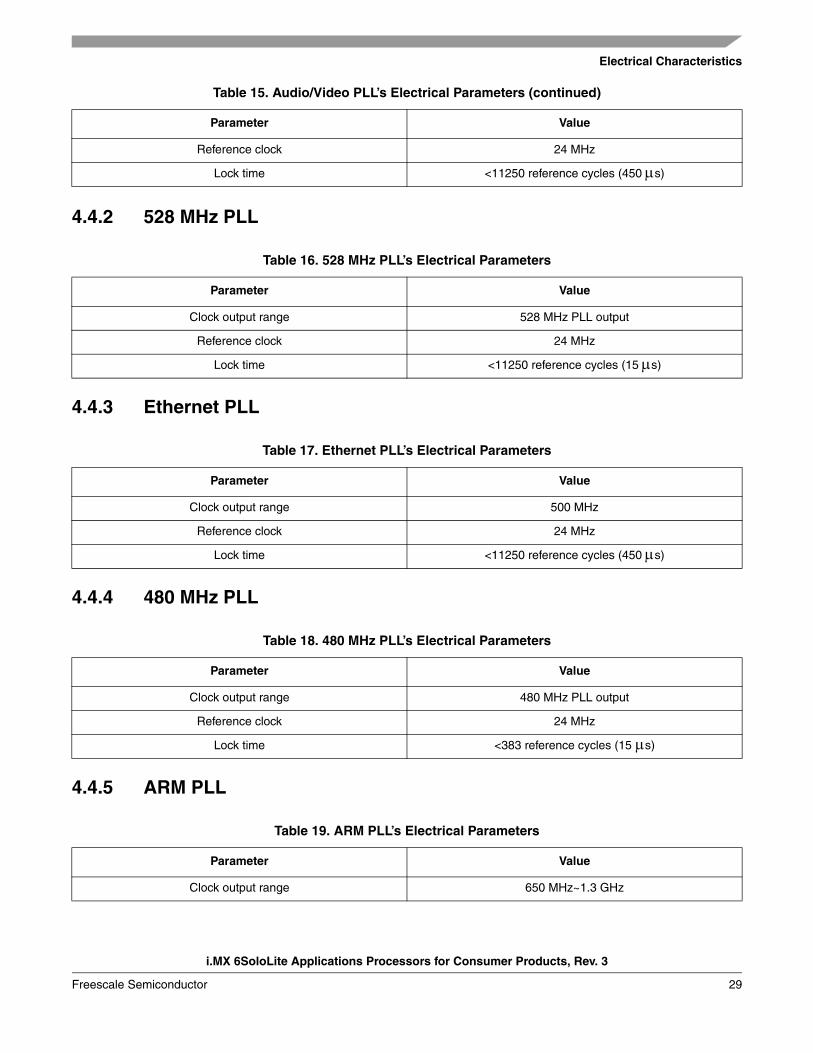
4.4 PLL’s Electrical Characteristics
4.4.1 Audio/Video PLL’s Electrical Parameters
Table 15. Audio/Video PLL’s Electrical Parameters
Parameter Value
Clock output range 650 MHz ~1.3 GHz
Electrical Characteristics
i.MX 6SoloLite Applications Processors for Consumer Products, Rev. 3
i.MX 6SoloLite Applications Processors for Consumer Products, Rev. 3
30 Freescale Semiconductor
Electrical Characteristics
4.5 On-Chip Oscillators
4.5.1 OSC24M
This block implements an amplifier that when combined with a suitable quartz crystal and external load capacitors implements an oscillator. It also implements a power mux such that the oscillator can be powered from NVCC_1P2V or VDD_SOC. NVCC_1P2V should be the cleaner supply and is the preferable choice, however, if the oscillator is required to run in stop mode then it is necessary to run from VDD_SOC, which is 0.9 V in stop mode.
The system crystal oscillator consists of a Pierce-type structure running off the digital supply. A straight forward biased-inverter implementation is used.
4.5.2 OSC32K
This block implements an amplifier that when combined with a suitable quartz crystal and external load capacitors implements a low power oscillator. It also implements a power mux such that it can be powered from either a ~3 V backup battery (VDD_SNVS_IN) or VDD_HIGH_IN such as the oscillator consumes power from VDD_HIGH_IN when that supply is available and transitions to the back up battery when VDD_HIGH_IN is lost.
In addition, if the clock monitor determines that the OSC32K is not present, then the source of the 32 kHz clock will automatically switch to the internal ring oscillator.
CAUTIONThe internal RTC oscillator does not provide an accurate frequency and is affected by process, voltage and temperature variations. Freescale strongly recommends using an external crystal as the RTC_XTALI reference. If the internal oscillator is used instead, careful consideration must be given to the timing implications on all of the SoC modules dependent on this clock.
The OSC32k runs from VDD_SNVS_CAP, which comes from the VDD_HIGH_IN/VDD_SNVS_IN power mux. The target battery is a ~3 V coin cell. Proper choice of coin cell type is necessary for chosen VDD_HIGH_IN range. Appropriate series resistor (Rs) must be used when connecting the coin cell. Rs depends on the charge current limit that depends on the chosen coin cell. For example, for Panasonic ML621:
• Average Discharge Voltage is 2.5 V
• Maximum Charge Current is 0.6 mA
For a charge voltage of 3.2 V, Rs = (3.2-2.5)/0.6 m = 1.17 k
Reference clock 24 MHz
Lock time <2250 reference cycles (50 s)
Table 19. ARM PLL’s Electrical Parameters (continued)
Parameter Value
Electrical Characteristics
i.MX 6SoloLite Applications Processors for Consumer Products, Rev. 3
Freescale Semiconductor 31
NOTEAlways refer to the chosen coin cell manufacturer's data sheet for the latest information.
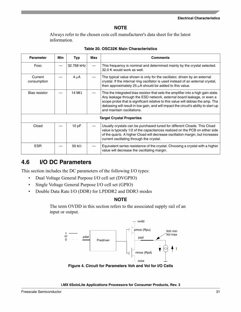
4.6 I/O DC ParametersThis section includes the DC parameters of the following I/O types:
• Dual Voltage General Purpose I/O cell set (DVGPIO)
• Single Voltage General Purpose I/O cell set (GPIO)
• Double Data Rate I/O (DDR) for LPDDR2 and DDR3 modes
NOTEThe term OVDD in this section refers to the associated supply rail of an input or output.
Figure 4. Circuit for Parameters Voh and Vol for I/O Cells
Table 20. OSC32K Main Characteristics
Parameter Min Typ Max Comments
Fosc — 32.768 kHz — This frequency is nominal and determined mainly by the crystal selected. 32.0 K would work as well.
Currentconsumption
— 4 A — The typical value shown is only for the oscillator, driven by an external crystal. If the internal ring oscillator is used instead of an external crystal, then approximately 25 A should be added to this value.
Bias resistor — 14 M — This the integrated bias resistor that sets the amplifier into a high gain state. Any leakage through the ESD network, external board leakage, or even a scope probe that is significant relative to this value will debias the amp. The debiasing will result in low gain, and will impact the circuit's ability to start up and maintain oscillations.
Target Crystal Properties
Cload — 10 pF — Usually crystals can be purchased tuned for different Cloads. This Cload value is typically 1/2 of the capacitances realized on the PCB on either side of the quartz. A higher Cload will decrease oscillation margin, but increases current oscillating through the crystal.
ESR — 50 k — Equivalent series resistance of the crystal. Choosing a crystal with a higher value will decrease the oscillating margin.
0or1
Predriverpdat
ovdd
pad
nmos (Rpd)
ovss
Voh minVol max
pmos (Rpu)
i.MX 6SoloLite Applications Processors for Consumer Products, Rev. 3
32 Freescale Semiconductor
Electrical Characteristics
4.6.1 XTALI and RTC_XTALI (Clock Inputs) DC Parameters
Table 21 shows the DC parameters for the clock inputs.
4.6.2 Dual Voltage General Purpose IO cell set (DVGPIO) DC Parameters
Table 22 shows DC parameters for GPIO pads. The parameters in Table 23 are guaranteed per the operating ranges in Table 9, unless otherwise noted.
Table 21. XTALI and RTC_XTALI DC Parameters
Parameter Symbol Test Conditions Min Max Unit
XTALI high-level DC input voltage Vih — 0.8 x NVCC_PLL_OUT NVCC_PLL_ OUT V
XTALI low-level DC input voltage Vil — 0 0.2V V
RTC_XTALI high-level DC input voltage Vih — 0.8 1.1 V
RTC_XTALI low-level DC input voltage Vil — 0 0.2V V
Table 22. DVGPIO I/O DC Parameters
Parameter Symbol Test Conditions Min Max Unit
High-level output voltage1 Voh Ioh = -0.1 mA (DSE2 = 001, 010)Ioh = -1 mA
High-Level DC input voltage1, 3 Vih — 0.7 OVDD OVDD V
Low-Level DC input voltage1, 3 Vil — 0 0.3 OVDD V
Input Hysteresis Vhys OVDD = 1.8 VOVDD = 3.3 V
0.25 — V
Schmitt trigger VT+3, 4 VT+ — 0.5 OVDD — V
Schmitt trigger VT–3, 4 VT– — — 0.5 OVDD V
Input current (no pull-up/down) Iin Vin = OVDD or 0 -1.25 1.25 A
Input current (22 k pull-up) Iin Vin = 0 VVin = OVDD
— 2121
A
Input current (47 k pull-up) Iin Vin = 0 VVin = OVDD
— 1001
A
Input current (100 k pull-up) Iin Vin = 0 VVin= OVDD
— 481
A
Input current (100 k pull-down) Iin Vin = 0 VVin = OVDD
— 148
A
Keeper circuit resistance Rkeep Vin = 0.3 x OVDDVin = 0.7 x OVDD
105 205k
Electrical Characteristics
i.MX 6SoloLite Applications Processors for Consumer Products, Rev. 3
Freescale Semiconductor 33
4.6.3 Single Voltage General Purpose I/O (GPIO) DC Parameters
Table 23 shows DC parameters for GPIO pads. The parameters in Table 23 are guaranteed per the operating ranges in Table 9, unless otherwise noted.
1 Overshoot and undershoot conditions (transitions above OVDD and below GND) on switching pads must be held below 0.6 V, and the duration of the overshoot/undershoot must not exceed 10% of the system clock cycle. Overshoot/ undershoot must be controlled through printed circuit board layout, transmission line impedance matching, signal line termination, or other methods. Non-compliance to this specification may affect device reliability or cause permanent damage to the device.
2 DSE is the Drive Strength Field setting in the associated IOMUX control register.3 To maintain a valid level, the transition edge of the input must sustain a constant slew rate (monotonic) from the current DC
level through to the target DC level, Vil or Vih. Monotonic input transition time is from 0.1 ns to 1 s.4 Hysteresis of 250 mV is guaranteed over all operating conditions when hysteresis is enabled.
Table 23. GPIO I/O DC Parameters
Parameter Symbol Test Conditions Min Max Unit
High-level output voltage1
1 Overshoot and undershoot conditions (transitions above OVDD and below GND) on switching pads must be held below 0.6 V, and the duration of the overshoot/undershoot must not exceed 10% of the system clock cycle. Overshoot/ undershoot must be controlled through printed circuit board layout, transmission line impedance matching, signal line termination, or other methods. Non-compliance to this specification may affect device reliability or cause permanent damage to the device.
Voh Ioh = -0.1 mA (DSE2 = 001, 010)Ioh = -1 mA (DSE = 011, 100, 101, 110, 111)
2 DSE is the Drive Strength Field setting in the associated IOMUX control register.
3 To maintain a valid level, the transition edge of the input must sustain a constant slew rate (monotonic) from the current DC level through to the target DC level, Vil or Vih. Monotonic input transition time is from 0.1 ns to 1 s.
Vih — 0.7 OVDD OVDD V
Low-Level DC input voltage1, 3 Vil — 0 0.3 OVDD V
Input Hysteresis Vhys OVDD = 3.3 V 0.25 — V
Schmitt trigger VT+3, 4
4 Hysteresis of 250 mV is guaranteed over all operating conditions when hysteresis is enabled.
VT+ — 0.5 OVDD — V
Schmitt trigger VT–3, 4 VT– — — 0.5 OVDD V
Input current (no pull-up/down) Iin Vin = OVDD or 0 -1.25 1.25 A
Input current (22 k pull-up) Iin Vin = 0 VVin = OVDD
— 2121
A
Input current (47 k pull-up) Iin Vin = 0 VVin = OVDD
— 1001
A
Input current (100 k pull-up) Iin Vin = 0 VVin= OVDD
— 481
A
Input current (100 k pull-down) Iin Vin = 0 VVin = OVDD
— 148
A
Keeper circuit resistance Rkeep Vin = 0.3 x OVDDVin = 0.7 x OVDD
105 205k
i.MX 6SoloLite Applications Processors for Consumer Products, Rev. 3
34 Freescale Semiconductor
Electrical Characteristics
4.6.4 DDR I/O DC Parameters
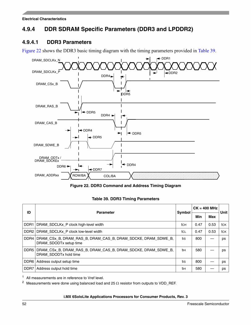
The DDR I/O pads support LPDDR2 and DDR3 operational modes.
4.6.4.1 LPDDR2 Mode I/O DC Parameters
The LPDDR2 interface mode fully complies with JESD209-2B LPDDR2 JEDEC standard release June, 2009. The parameters in Table 24 are guaranteed per the operating ranges in Table 9, unless otherwise noted.
4.6.4.2 DDR3 Mode I/O DC Parameters
The DDR3 interface mode fully complies with JESD79-3D DDR3 JEDEC standard release April, 2008. The parameters in Table 25 are guaranteed per the operating ranges in Table 9, unless otherwise noted.
4.7 I/O AC Parameters
Table 24. LPDDR2 I/O DC Electrical Parameters1
1 Note that the JEDEC LPDDR2 specification (JESD209_2B) supersedes any specification in this document.
Parameters Symbol Test Conditions Min Max Unit
High-level output voltage Voh Ioh = -0.1 mA 0.9 OVDD — V
Low-level output voltage Vol Iol = 0.1 mA — 0.1 OVDD V
Input reference voltage Vref — 0.49 OVDD 0.51 OVDD
DC input High Voltage Vih(dc) — Vref+0.13V OVDD V
DC input Low Voltage Vil(dc) — OVSS Vref-0.13V V
Differential Input Logic High Vih(diff) — 0.26 See Note 2
2 The single-ended signals need to be within the respective limits (Vih(dc) max, Vil(dc) min) for single-ended signals as well as the limitations for overshoot and undershoot (see Table 28).
Differential Input Logic Low Vil(diff) — See Note 2 -0.26
Input current (no pull-up/down) Iin Vin = 0 or OVDD -2.5 2.5 A
1 OVDD – I/O power supply (1.425 V–1.575 V for DDR3)2 Vref – DDR3 external reference voltage3 The single-ended signals need to be within the respective limits (Vih(dc) max, Vil(dc) min) for single-ended signals as well as
the limitations for overshoot and undershoot (see Table 29).4 Use an off-chip pull resistor of 10 kor less to override this keeper.
Table 25. DDR3 I/O DC Electrical Parameters (continued)
Parameters Symbol Test Conditions Min Max Unit
Test PointFrom Output
CL
CL includes package, probe and fixture capacitance
Under Test
0 V
OVDD
20%
80% 80%
20%
tr tfOutput (at pad)
i.MX 6SoloLite Applications Processors for Consumer Products, Rev. 3
36 Freescale Semiconductor
Electrical Characteristics
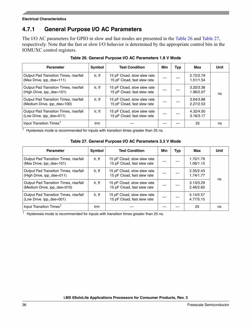
4.7.1 General Purpose I/O AC Parameters
The I/O AC parameters for GPIO in slow and fast modes are presented in the Table 26 and Table 27, respectively. Note that the fast or slow I/O behavior is determined by the appropriate control bits in the IOMUXC control registers.
Table 26. General Purpose I/O AC Parameters 1.8 V Mode
Parameter Symbol Test Condition Min Typ Max Unit
Output Pad Transition Times, rise/fall(Max Drive, ipp_dse=111)
1 Hysteresis mode is recommended for inputs with transition times greater than 25 ns.
trm — — — 25 ns
Electrical Characteristics
i.MX 6SoloLite Applications Processors for Consumer Products, Rev. 3
Freescale Semiconductor 37
4.7.2 DDR I/O AC Parameters
The LPDDR2 interface mode fully complies with JESD209-2B LPDDR2 JEDEC standard release June, 2009. The DDR3 interface mode fully complies with JESD79-3D DDR3 JEDEC standard release April, 2008.
Table 28 shows the AC parameters for DDR I/O operating in LPDDR2 mode.
Table 29 shows the AC parameters for DDR I/O operating in DDR3 mode.
Table 28. DDR I/O LPDDR2 Mode AC Parameters1
1 Note that the JEDEC LPDDR2 specification (JESD209_2B) supersedes any specification in this document.
Parameter Symbol Test Condition Min Typ Max Unit
AC input logic high Vih(ac) — Vref + 0.22 — OVDD V
AC input logic low Vil(ac) — 0 — Vref – 0.22 V
AC differential input high voltage2
2 Vid(ac) specifies the input differential voltage |Vtr – Vcp| required for switching, where Vtr is the “true” input signal and Vcp is the “complementary” input signal. The Minimum value is equal to Vih(ac) – Vil(ac).
Vidh(ac) — 0.44 — — V
AC differential input low voltage Vidl(ac) — — — 0.44 V
Input AC differential cross point voltage3
3 The typical value of Vix(ac) is expected to be about 0.5 OVDD. and Vix(ac) is expected to track variation of OVDD. Vix(ac) indicates the voltage at which differential input signal must cross.
Vix(ac) Relative to Vref -0.12 — 0.12 V
Over/undershoot peak Vpeak — — — 0.35 V
Over/undershoot area (above OVDDor below OVSS)
Varea 400 MHz — — 0.3 V-ns
Single output slew rate, measured between Vol (ac) and Voh (ac)
tsr 50 to Vref.5 pF load.
Drive impedance = 4 0 30%
1.5 — 3.5
V/ns50 to Vref.
5pF load.Drive impedance = 60 30%
1 — 2.5
Skew between pad rise/fall asymmetry + skew caused by SSN
tSKD clk = 400 MHz — — 0.1 ns
Table 29. DDR I/O DDR3 Mode AC Parameters1
Parameter Symbol Test Condition Min Typ Max Unit
AC input logic high Vih(ac) — Vref + 0.175 — OVDD V
AC input logic low Vil(ac) — 0 — Vref – 0.175 V
AC differential input voltage2 Vid(ac) — 0.35 — — V
Input AC differential cross point voltage3 Vix(ac) Relative to Vref Vref – 0.15 — Vref + 0.15 V
Over/undershoot peak Vpeak — — — 0.4 V
Over/undershoot area (above OVDDor below OVSS)
Varea 400 MHz — — 0.5 V-ns
i.MX 6SoloLite Applications Processors for Consumer Products, Rev. 3
38 Freescale Semiconductor
Electrical Characteristics
4.8 Output Buffer Impedance ParametersThis section defines the I/O impedance parameters of the i.MX 6SoloLite processor for the following I/O types:
• Dual Voltage General Purpose I/O cell set (DVGPIO)
• Single Voltage General Purpose I/O cell set (GPIO)
• Double Data Rate I/O (DDR) for LPDDR2, and DDR3 modes
NOTEGPIO and DDR I/O output driver impedance is measured with “long” transmission line of impedance Ztl attached to I/O pad and incident wave launched into transmission line. Rpu/Rpd and Ztl form a voltage divider that defines specific voltage of incident wave relative to OVDD. Output driver impedance is calculated from this voltage divider (see Figure 7).
Single output slew rate, measured between Vol (ac) and Voh (ac)
tsr Driver impedance = 34 2.5 — 5 V/ns
Skew between pad rise/fall asymmetry + skew caused by SSN
tSKD clk = 400 MHz — — 0.1 ns
1 Note that the JEDEC JESD79_3C specification supersedes any specification in this document.2 Vid(ac) specifies the input differential voltage |Vtr-Vcp| required for switching, where Vtr is the “true” input signal and Vcp is the
“complementary” input signal. The Minimum value is equal to Vih(ac) – Vil(ac).3 The typical value of Vix(ac) is expected to be about 0.5 OVDD. and Vix(ac) is expected to track variation of OVDD. Vix(ac)
indicates the voltage at which differential input signal must cross.
Table 29. DDR I/O DDR3 Mode AC Parameters1 (continued)
Parameter Symbol Test Condition Min Typ Max Unit
Electrical Characteristics
i.MX 6SoloLite Applications Processors for Consumer Products, Rev. 3
Freescale Semiconductor 39
Figure 7. Impedance Matching Load for Measurement
4.8.1 Dual Voltage GPIO Output Buffer Impedance Table 30 shows the GPIO output buffer impedance (OVDD 1.8 V).
Table 30. DVGPIO Output Buffer Average Impedance (OVDD 1.8 V)
Parameter Symbol Drive Strength (ipp_dse) Typ Value Unit
Output Driver Impedance
Rdrv
001010011100101110111
2601309060504033
ipp_do
Cload = 1p
Ztl , L = 20 inches
predriver
PMOS (Rpu)
NMOS (Rpd)
pad
OVDD
OVSS
t,(ns)
U,(V)
OVDD
t,(ns)0
VDDVin (do)
Vout (pad)U,(V)
Vref
Rpu = Vovdd – Vref1
Vref1 Ztl
Rpd = ZtlVref2
Vovdd – Vref2
Vref1 Vref2
0
i.MX 6SoloLite Applications Processors for Consumer Products, Rev. 3
4.8.2 Single Voltage GPIO Output Buffer ImpedanceTable 32 shows the GPIO output buffer impedance (OVDD 3.3 V).
4.8.3 DDR I/O Output Buffer Impedance
The LPDDR2 interface fully complies with JESD209-2B LPDDR2 JEDEC standard release June, 2009. The DDR3 interface fully complies with JESD79-3D DDR3 JEDEC standard release April, 2008.
Note: 1. Output driver impedance is controlled across PVTs using ZQ calibration procedure.2. Calibration is done against 240 W external reference resistor.
3. Output driver impedance deviation (calibration accuracy) is ±5% (max/min impedance) across PVTs.
Table 31. DVGPIO Output Buffer Average Impedance (OVDD 3.3 V)
Parameter Symbol Drive Strength (ipp_dse) Typ Value Unit
Output Driver Impedance
Rdrv
001010011100101110111
150755037302520
Table 32. GPIO Output Buffer Average Impedance (OVDD 3.3 V)
Parameter Symbol Drive Strength (ipp_dse) Typ Value Unit
Output Driver Impedance
Rdrv
001010011100101110111
150755037302520
Table 33. DDR I/O Output Buffer Impedance
Parameter Symbol Test Conditions
Typical
UnitNVCC_DRAM=1.5 V (DDR3)
DDR_SEL=11
NVCC_DRAM=1.2 V (LPDDR2)
DDR_SEL=10
Output Driver Impedance
Rdrv
Drive Strength (DSE) =000001010011100101110111
Hi-Z2401208060484034
Hi-Z2401208060484034
Electrical Characteristics
i.MX 6SoloLite Applications Processors for Consumer Products, Rev. 3
Freescale Semiconductor 41
4.9 System Modules TimingThis section contains the timing and electrical parameters for the modules in each i.MX 6SoloLite processor.
4.9.1 Reset Timings ParametersFigure 8 shows the reset timing and Table 34 lists the timing parameters.
Figure 8. Reset Timing Diagram
4.9.2 WDOG Reset Timing ParametersFigure 9 shows the WDOG reset timing and Table 35 lists the timing parameters.
Figure 9. WDOG_B Timing Diagram
NOTERTC_XTALI is approximately 32 kHz. RTC_XTALI cycle is one period or approximately 30 s.
NOTEWDOG_B output signals (for each one of the Watchdog modules) do not have dedicated bins, but are muxed out through the IOMUX. See the IOMUX manual for detailed information.
Table 34. Reset Timing Parameters
ID Parameter Min Max Unit
CC1 Duration of POR_B to be qualified as valid. 1 — XTALOSC_RTC_XTALI
Table 35. WDOG_B Timing Parameters
ID Parameter Min Max Unit
CC3 Duration of WDOG_B Assertion 1 — RTC_XTALI cycle
SRC_POR_B
CC1(Input)
WDOG_B
CC3(Output)
i.MX 6SoloLite Applications Processors for Consumer Products, Rev. 3
42 Freescale Semiconductor
Electrical Characteristics
4.9.3 External Interface Module (EIM)
The following subsections provide information on the EIM. The maximum operating frequency for EIM data transfer is 104 MHz. Timing parameters in this section that are given as a function of register settings or clock periods are valid for the entire range of allowed frequencies (0–104 MHz).
4.9.3.1 EIM Interface Pads Allocation
EIM supports 32-bit, 16-bit, and 8-bit devices operating in address/data separate or multiplexed modes. Table 36 provides EIM interface pads allocation in different modes.
Table 36. EIM Internal Module Multiplexing1
1 For more information on configuration ports mentioned in this table, see the i.MX 6SololLite reference manual.
Setup
Non Multiplexed Address/Data Mode Multiplexed Address/Data mode
8 Bit 16 Bit 16 Bit 32 Bit
MUM = 0, DSZ = 100
MUM = 0, DSZ = 101
MUM = 0, DSZ = 001
MUM = 1, DSZ = 001
MUM = 1, DSZ = 011
EIM_ADDR[15:00]
EIM_AD[15:00]
EIM_AD[15:00]
EIM_AD[15:00]
EIM_AD [15:00]
EIM_AD [15:00]
EIM_ADDR[25:16]
EIM_ADDR[25:16]
EIM_ADDR[25:16]
EIM_ADDR[25:16]
EIM_ADDR[25:16]
EIM_DATA[09:00]
EIM_DATA[07:00],
EIM_EB0_B
EIM_DATA[07:00]
— EIM_DATA[07:00]
EIM_AD [07:00]
EIM_AD [07:00]
EIM_DATA[15:08],
EIM_EB1_B
— EIM_DATA[15:08]
EIM_DATA[15:08]
EIM_AD [15:08]
EIM_AD[15:08]
EIM_DATA[23:16],
EIM_EB2_B
— — — — EIM_DATA[07:00]
EIM_DATA[31:24],
EIM_EB3_B
— — — — EIM_DATA[15:08]
Electrical Characteristics
i.MX 6SoloLite Applications Processors for Consumer Products, Rev. 3
Freescale Semiconductor 43
4.9.3.2 General EIM Timing-Synchronous Mode
Figure 10, Figure 11, and Table 37 specify the timings related to the EIM module. All EIM output control signals may be asserted and deasserted by an internal clock synchronized to the BCLK rising edge according to corresponding assertion/negation control fields.
,
Figure 10. EIM Output Timing Diagram
Figure 11. EIM Input Timing Diagram
4.9.3.3 Examples of EIM Synchronous Accesses
Table 37. EIM Bus Timing Parameters
ID Parameter Min1 Max1 Unit
WE1 EIM_BCLK cycle time2 t (k+1) — ns
WE2 EIM_BCLK high level width 0.4 t (k+1) — ns
WE3 EIM_BCLK low level width 0.4 t (k+1) — ns
WE4 Clock rise to address valid — -0.5 t (k+1)/2+2.25 ns
WE4
EIM_ADDR
EIM_CSx_B
EIM_RW_B
EIM_OE_B
EIM_BCLK
EIM_EBx_B
EIM_LBA_B
Output Data
...
WE5
WE6 WE7
WE8 WE9
WE10 WE11
WE12 WE13
WE14 WE15
WE16 WE17
WE3
WE2
WE1
Input Data
EIM_WAIT_B
EIM_BCLK
WE19
WE18
WE21
WE20
i.MX 6SoloLite Applications Processors for Consumer Products, Rev. 3
44 Freescale Semiconductor
Electrical Characteristics
WE5 Clock rise to address invalid 0.5 t (k+1)/2-1.25 — ns
WE6 Clock rise to EIM_CSx_B valid — -0.5 t (k+1)/2+2.25 ns
WE7 Clock rise to EIM_CSx_B invalid 0.5 t (k+1)/2-1.25 — ns
WE8 Clock rise to EIM_RW_B valid — -0.5 t (k+1)/2+2.25 ns
WE9 Clock rise to EIM_RW_B invalid 0.5 t (k+1)/2-1.25 — ns
WE10 Clock rise to EIM_OE_B valid — -0.5 t (k+1)/2+2.25 ns
WE11 Clock rise to EIM_OE_B invalid 0.5 t (k+1)/2-1.25 — ns
WE12 Clock rise to EIM_EBx_B valid — -0.5 t (k+1)/2+2.25 ns
WE13 Clock rise to EIM_EBx_B invalid 0.5 t (k+1)/2-1.25 — ns
WE14 Clock rise to EIM_LBA_B valid — -0.5 t (k+1)/2+2.25 ns
WE15 Clock rise to EIM_LBA_B invalid 0.5 t (k+1)/2-1.25 — ns
WE16 Clock rise to output data valid — -(k+1) t/2+2.75 ns
WE17 Clock rise to output data invalid (k+1) t/2-1.25 — ns
WE18 Input data setup time to clock rise 2.3 — ns
WE19 Input data hold time from clock rise 2 — ns
WE20 EIM_WAIT_B setup time to clock rise 2 — ns
WE21 EIM_WAIT_B hold time from clock rise 2 — ns
1 k represents register setting BCD value2 t is clock period (1/Freq). For 104 MHz, t = 9.165 ns
Table 37. EIM Bus Timing Parameters (continued)
ID Parameter Min1 Max1 Unit
Electrical Characteristics
i.MX 6SoloLite Applications Processors for Consumer Products, Rev. 3
Freescale Semiconductor 45
Figure 12 to Figure 15 provide few examples of basic EIM accesses to external memory devices with the timing parameters mentioned previously for specific control parameters settings.
Figure 12. Synchronous Memory Read Access, WSC=1
Figure 13. Synchronous Memory, Write Access, WSC=1, WBEA=0 and WADVN=0
Last Valid Address Address v1
D(v1)
EIM_BCLK
EIM_ADDRxx
EIM_DATAxx
EIM_RW_B
EIM_LBA_B
EIM_OE_B
EIM_EBx_B
EIM_CSx_B
WE4 WE5
WE6 WE7
WE10 WE11
WE13WE12
WE14
WE15
WE18
WE19
Last Valid Address Address V1
D(V1)
EIM_BCLK
EIM_ADDRxx
EIM_DATAxx
EIM_RW_B
EIM_LBA_B
EIM_OE_B
EIM_EBx_B
EIM_CSx_B
WE4 WE5
WE6 WE7
WE8 WE9
WE12WE13
WE14
WE15
WE16 WE17
i.MX 6SoloLite Applications Processors for Consumer Products, Rev. 3
Figure 16 through Figure 20, and Table 38 help you determine timing parameters relative to the chip select (CS) state for asynchronous and DTACK EIM accesses with corresponding EIM bit fields and the timing parameters mentioned above.
Asynchronous read and write access length in cycles may vary from what is shown in Figure 16 through Figure 19 as RWSC, OEN & CSN is configured differently. See the i.MX 6SoloLite reference manual for the EIM programming model.
EIM_BCLK
EIM_ADDRxx/
EIM_RW_B
EIM_LBA_B
EIM_OE_B
EIM_EBx_B
EIM_CSx_B
Address V1 Write DataEIM_DATAxx
WE4WE16
WE6 WE7
WE9WE8
WE10 WE11
WE14 WE15
WE17WE5
Last AddressValid
WE4
Last
EIM_BCLK
EIM_ADDRxx/
EIM_RW_B
EIM_LBA_B
EIM_OE_B
EIM_EBx_B
EIM_CSx_B
Address V1 DataAddressEIM_DATAxx
WE5
WE6
WE7
WE14WE15
WE10WE11
WE12 WE13
WE18
WE19
Valid
Electrical Characteristics
i.MX 6SoloLite Applications Processors for Consumer Products, Rev. 3
WE37 EIM_CSx_B Valid to EIM_EBx_B Valid (Read access)
WE12-WE6+(RBEA-CSA) — 3+(RBEA7-CSA) ns
WE38 EIM_EBx_B Invalid to EIM_CSx_B Invalid (Read access)
WE7-WE13+(RBEN-CSN) — 4-(RBEN8-CSN) ns
WE39 EIM_CSx_B Valid to EIM_LBA_B Valid
WE14-WE6+(ADVA-CSA) — 3+(ADVA-CSA) ns
WE40 EIM_LBA_B Invalid to EIM_CSx_B Invalid (ADVL is asserted)
WE7-WE15-CSN — 3-CSN ns
WE40A(muxed A/D)
EIM_CSx_B Valid to EIM_LBA_B Invalid
WE14-WE6+(ADVN+ADVA+1-CSA)
-3 + (ADVN + ADVA + 1 - CSA)
3+(ADVN+ADVA+1-CSA)
ns
WE41 EIM_CSx_B Valid to Output Data Valid
WE16-WE6-WCSA — 3-WCSA ns
WE41A(muxed A/D)
EIM_CSx_B Valid to Output Data Valid
WE16-WE6+(WADVN+WADVA+ADH+1-WCSA)
— 3+(WADVN+WADVA+ADH+1-WCSA)
ns
WE42 Output Data Invalid to EIM_CSx_B Invalid
WE17-WE7-CSN — 3-CSN ns
MAXCO Output maximum delay from internal driving ADDR/control FFs to chip outputs
10 — — ns
MAXCSO Output maximum delay from CSx internal driving FFs to EIM_CSx_B out
10 — — ns
MAXDI Data maximum delay from chip input data to its internal FF
6 — — ns
Electrical Characteristics
i.MX 6SoloLite Applications Processors for Consumer Products, Rev. 3
Freescale Semiconductor 51
WE43 Input Data Valid to EIM_CSx_B Invalid
MAXCO-MAXCSO+MAXDI MAXCO-MAXCSO+MAXDI
— ns
WE44 EIM_CSx_B Invalid to Input Data Invalid
0 0 — ns
WE45 EIM_CSx_B Valid to EIM_EBx_B Valid (Write access)
WE12-WE6+(WBEA-CSA) — 3 + (WBEA - CSA) ns
WE46 EIM_EBx_B Invalid to EIM_CSx_B Invalid (Write access)
WE7-WE13+(WBEN-CSN) — -3 + (WBEN - CSN) ns
MAXDTI EIM_DTACK_B maximum delay from chip dtack input to its internal FF + 2 cycles for synchronization
10 — — ns
WE47 EIM_DTACK_B Active to EIM_CSx_B Invalid
MAXCO-MAXCSO+MAXDTI
MAXCO-MAXCSO+MAXDTI
— ns
WE48 EIM_CSx_B Invalid to EIM_DTACK_B invalid
0 0 — ns
1 For more information on configuration parameters mentioned in this table, see the i.MX 6SoloLite reference manual.2 CSA means register setting for WCSA when in write operations or RCSA when in read operations.3 CSN means register setting for WCSN when in write operations or RCSN when in read operations.4 t means clock period from axi_clk frequency.5 ADVA means register setting for WADVA when in write operations or RADVA when in read operations.6 ADVN means register setting for WADVN when in write operations or RADVN when in read operations.7 BEAssertion.ThisbitfielddetermineswhenBEsignalisassertedduringreadcycles.8 BENegation.ThisbitfielddetermineswhenBEsignalisnegatedduringreadcycles.
DDR4 DRAM_CSx_B, DRAM_RAS_B, DRAM_CAS_B, DRAM_SDCKE, DRAM_SDWE_B, DRAM_SDODTx setup time
tIS 800 — ps
DDR5 DRAM_CSx_B, DRAM_RAS_B, DRAM_CAS_B, DRAM_SDCKE, DRAM_SDWE_B, DRAM_SDODTx hold time
tIH 580 — ps
DDR6 Address output setup time tIS 800 — ps
DDR7 Address output hold time tIH 580 — ps
DRAM_SDWE_B
DRAM_ADDRxx ROW/BA COL/BA
DDR1
DDR2DDR4
DDR4
DDR5
DDR5
DDR5DDR5
DDR6DDR7
DRAM_SDCLKx_P
DRAM_ODTx /
DDR4DRAM_SDCKEx
DRAM_SDCLKx_N
DRAM_CSx_B
DRAM_RAS_B
DRAM_CAS_B
DDR4
Electrical Characteristics
i.MX 6SoloLite Applications Processors for Consumer Products, Rev. 3
Freescale Semiconductor 53
Figure 23 shows the DDR3 write timing diagram. The timing parameters for this diagram appear in Table 40.
Figure 23. DDR3 Write Cycle
1 To receive the reported setup and hold values, write calibration should be performed in order to locate the DRAM_SDQSx_P in the middle of DRAM_DATAxx window.
2 All measurements are in reference to Vref level.3 Measurements were taken using balanced load and 25 resistor from outputs to DRAM_VREF.
Table 40. DDR3 Write Cycle
ID Parameter SymbolCK = 400MHz
UnitMin Max
DDR17 DRAM_DATAxx and DRAM_DQMx setup time to DRAM_SDQSx_P (differential strobe)
tDS 420 — ps
DDR18 DRAM_DATAxx and DRAM_DQMx hold time to DRAM_SDQSx_P (differential strobe)
i.MX 6SoloLite Applications Processors for Consumer Products, Rev. 3
54 Freescale Semiconductor
Electrical Characteristics
Figure 24 shows the DDR3 read timing diagram. The timing parameters for this diagram appear in Table 41.
Figure 24. DDR3 Read Cycle
1 To receive the reported setup and hold values, read calibration should be performed in order to locate the DRAM_SDQSx_P in the middle of DRAM_DATAxx window.
2 All measurements are in reference to Vref level.3 Measurements were done using balanced load and 25 resistor from outputs to VDD_REF.
4.9.4.2 LPDDR2 Parameters
Figure 25 shows the LPDDR2 basic timing diagram. The timing parameters for this diagram appear in Table 42.
Figure 25. LPDDR2 Command and Address Timing Diagram
LP22 DRAM_SDQSx_P high level width tDQSH 0.4 — tCK
LP23 DRAM_SDQSx_P low level width tDQSL 0.4 — tCK
DRAM_SDCLKx_P
DRAM_SDCLKx_N
DRAM_SDCLKx_P
DRAM_DATAxx
DRAM_DQMx
Data Data Data Data Data Data Data Data
DM DM DM DM DM DM DM DM
LP17
LP17
LP17
LP17
LP18LP18
LP18 LP18
LP21LP23
LP22(output)
(output)
(output)
i.MX 6SoloLite Applications Processors for Consumer Products, Rev. 3
56 Freescale Semiconductor
Electrical Characteristics
1 To receive the reported setup and hold values, write calibration should be performed in order to locate the DRAM_SDQS in the middle of DRAM_DATAxx window.
2 All measurements are in reference to Vref level.3 Measurements were done using balanced load and 25 resistor from outputs to DRAM_VREF.
Figure 27 shows the LPDDR2 read timing diagram. The timing parameters for this diagram appear in Table 44.
Figure 27. LPDDR2 Read Cycle
1 To receive the reported setup and hold values, read calibration should be performed in order to locate the DRAM_SDQSx_P in the middle of DRAM_DATA_xx window.
2 All measurements are in reference to Vref level.3 Measurements were done using balanced load and 25 resistor from outputs to DRAM_VREF.
4.10 External Peripheral Interface ParametersThe following subsections provide information on external peripheral interfaces.
4.10.1 AUDMUX Timing Parameters
The AUDMUX provides a programmable interconnect logic for voice, audio, and data routing between internal serial interfaces (SSIs) and external serial interfaces (audio and voice codecs). The AC timing of AUDMUX external pins is governed by the SSI module. For more information, see the respective SSI electrical specifications found within this document.
Figure 28 and Figure 29 shows the gated clock mode timings for CSI, and Table 45 describes the timing parameters (P1–P7) shown in the figures. A frame starts with a rising/falling edge on CSI_VSYNC (VSYNC), then CSI_HSYNC (HSYNC) is asserted and holds for the entire line. The pixel clock, CSI_PIXCLK (PIXCLK), is valid as long as HSYNC is asserted.
Figure 28. CSI Gated Clock Mode—Sensor Data at Falling Edge, Latch Data at Rising Edge
Figure 29. CSI Gated Clock Mode—Sensor Data at Rising Edge, Latch Data at Falling Edge
CSI_PIXCLK
CSI_VSYNC
CSI_DATA[15:00]
P5
P1
P3 P4
CSI_HSYNC
P2 P6
P7
CSI_PIXCLK
CSI_VSYNC
CSI_DATA[15:00]
P6
P1
P3 P4
CSI_HSYNC
P2 P5
P7
i.MX 6SoloLite Applications Processors for Consumer Products, Rev. 3
58 Freescale Semiconductor
Electrical Characteristics
4.10.2.0.2 Ungated Clock Mode Timing
Figure 30 shows the ungated clock mode timings of CSI, and Table 46 describes the timing parameters (P1–P6) that are shown in the figure. In ungated mode the CSI_VSYNC and CSI_PIXCLK signals are used, and the CSI_HSYNC signal is ignored.
Figure 30. CSI Ungated Clock Mode—Sensor Data at Falling Edge, Latch Data at Rising Edge
The CSI enables the chip to connect directly to external CMOS image sensors, which are classified as dumb or smart as follows:
i.MX 6SoloLite Applications Processors for Consumer Products, Rev. 3
Freescale Semiconductor 59
• Dumb sensors only support traditional sensor timing (vertical sync (VSYNC) and horizontal sync (HSYNC)) and output-only Bayer and statistics data.
• Smart sensors support CCIR656 video decoder formats and perform additional processing of the image (for example, image compression, image pre-filtering, and various data output formats).
The following subsections describe the CSI timing in gated and ungated clock modes.
4.10.3 ECSPI Timing Parameters
This section describes the timing parameters of the ECSPI block. The ECSPI has separate timing parameters for master and slave modes.
4.10.3.1 ECSPI Master Mode Timing
Figure 31 depicts the timing of ECSPI in master mode and Table 47 lists the ECSPI master mode timing characteristics.
Figure 31. ECSPI Master Mode Timing Diagram
Table 47. ECSPI Master Mode Timing Parameters
ID Parameter Symbol Min Max Unit
CS1 ECSPIx_SCLK Cycle Time–Read • Slow group1
• Fast group2
ECSPIx_SCLK Cycle Time–Write
tclk464015
— ns
CS2 ECSPIx_SCLK High or Low Time–Read • Slow group1
• Fast group2
ECSPIx_SCLK High or Low Time–Write
tSW22207
— ns
CS3 ECSPIx_SCLK Rise or Fall3 tRISE/FALL — — ns
CS4 ECSPIx_SSx pulse width tCSLH Half ECSPIx period — ns
CS5 ECSPIx_SSx Lead Time (CS setup time) tSCS Half ECSPIx_SCLK period - 4 — ns
CS1
CS7
CS2
CS2
CS4
CS6 CS5
CS8 CS9
ECSPIx_SCLK
ECSPIx_SSx
ECSPIx_MOSI
ECSPIx_MISO
ECSPIx_RDY
CS10
CS3
CS3
i.MX 6SoloLite Applications Processors for Consumer Products, Rev. 3
60 Freescale Semiconductor
Electrical Characteristics
CS6 ECSPIx_SSx Lag Time (CS hold time) tHCS Half ECSPI_SCLK period - 2 — ns
1 ECSPI slow group includes:ECSPI2/EPDC_SDLE, ECSPI3/EPDC_D9, ECSPI4/EPDC_D1
2 ECSPI fast group includes:ECSPI1/LCD_DATA01, ECSPI1/ECSPI1_MISO, ECSPI2/LCD_DATA10, ECSPI2/ECSPI2_MISO, ECSPI3/AUDx_TXC, ECSPI3/SD2_DAT1, ECSPI4/KEY_ROW1, ECSPI4/FEC_RX_DV
3 See specific I/O AC parameters Section 4.7, “I/O AC Parameters.”4 ECSPIx_RDY is sampled internally by ipg_clk and is asynchronous to all other eCSPI signals.
i.MX 6SoloLite Applications Processors for Consumer Products, Rev. 3
62 Freescale Semiconductor
Electrical Characteristics
4.10.4 Ultra High Speed SD/SDIO/MMC Host Interface (uSDHC) AC Timing
This section describes the electrical information of the uSDHC, which includes SD/eMMC4.3 (Single Data Rate) timing and eMMC4.4/4.41 (Dual Date Rate) timing.
4.10.4.1 SD/eMMC4.3 (Single Data Rate) AC Timing
Figure 33 depicts the timing of SD/eMMC4.3, and Table 49 lists the SD/eMMC4.3 timing characteristics.
1 In low speed mode, card clock must be lower than 400 kHz, voltage ranges from 2.7 to 3.6 V.
0 400 kHz
Clock Frequency (SD/SDIO Full Speed/High Speed) fPP2
2 In normal (full) speed mode for SD/SDIO card, clock frequency can be any value between 0–25 MHz. In high-speed mode, clock frequency can be any value between 0–50 MHz.
0 25/50 MHz
Clock Frequency (MMC Full Speed/High Speed) fPP3
3 In normal (full) speed mode for MMC card, clock frequency can be any value between 0–20 MHz. In high-speed mode, clock frequency can be any value between 0–52 MHz.
0 20/52 MHz
Clock Frequency (Identification Mode) fOD 100 400 kHz
SD2 Clock Low Time tWL 7 — ns
SD3 Clock High Time tWH 7 — ns
eSDHC Output/Card Inputs SDx_CMD, SDx_DATAx (Reference to CLK)
SD6 eSDHC Output Delay tOD –6.6 3.6 ns
eSDHC Input/Card Outputs SDx_CMD, SDx_DATAx (Reference to CLK)
SD7 eSDHC Input Setup Time tISU 2.5 — ns
SD8 eSDHC Input Hold Time4
4To satisfy hold timing, the delay difference between clock input and cmd/data input must not exceed 2 ns.
tIH 1.5 — ns
SD1
SD3
SD5
SD4
SD7
SDx_CLK
SD2
SD8
SD6
Output from uSDHC to card
Input from card to uSDHCSDx_DATA[7:0]
SDx_DATA[7:0]
Electrical Characteristics
i.MX 6SoloLite Applications Processors for Consumer Products, Rev. 3
Freescale Semiconductor 63
4.10.4.2 eMMC4.4/4.41 (Dual Data Rate) eSDHCv3 AC Timing
Figure 34 depicts the timing of eMMC4.4/4.41. Table 50 lists the eMMC4.4/4.41 timing characteristics. Be aware that only SDx_DATAx is sampled on both edges of the clock (not applicable to SDx_CMD).
uSDHC Output/Card Inputs SD_CMD, SD_DATAx in SDR50 (Reference to CLK)
SD4 uSDHC Output Delay tOD –3 1 ns
uSDHC Output/Card Inputs SD_CMD, SD_DATAx in SDR104 (Reference to CLK)
SD5 uSDHC Output Delay1
1 If using KEY_COL1, KEY_ROW1, KEY_COL2 and KEY_ROW2 for SD3_DATA4–SD3_DATA7, note the difference in timing: tod minimum is -1.1 and tod maximum is 1.5.
tOD –1.6 1 ns
uSDHC Input/Card Outputs SD_CMD, SD_DATAx in SDR50 (Reference to CLK)
SD6 uSDHC Input Setup Time tISU 2.5 — ns
SD7 uSDHC Input Hold Time tIH 1.5 — ns
uSDHC Input/Card Outputs SD_CMD, SD_DATAx in SDR104 (Reference to CLK)2
2 Data window in SDR100 mode is variable.
SD8 Card Output Data Window tODW 0.5 tCLK — ns
SDx_SCLK
Electrical Characteristics
i.MX 6SoloLite Applications Processors for Consumer Products, Rev. 3
Freescale Semiconductor 65
4.10.5 FEC AC Timing Parameters
This section describes the electrical information of the Fast Ethernet Controller (FEC) module. The FEC is designed to support both 10 and 100 Mbps Ethernet/IEEE 802.3 networks. An external transceiver interface and transceiver function are required to complete the interface to the media. The FEC supports the 10/100 Mbps RMII (10 pins in total) and the 10 Mbps (only 7-wire interface, which uses 7 of the RMII pins), for connection to an external Ethernet transceiver. For the pin list of RMII and 7-wire, see the i.MX 6SoloLite Reference Manual.
This section describes the AC timing specifications of the FEC. The RMII signals are compatible with transceivers operating at a voltage of 3.3 V.
4.10.5.1 RMII Mode Timing
In RMII mode, FEC_TX_CLK is used as the REF_CLK which is a 50 MHz ±50 ppm continuous reference clock. FEC_RX_DV is used as the CRS_DV in RMII, and other signals under RMII mode include FEC_TX_EN, FEC_TX_DATA[1:0], FEC_RX_DATA[1:0] and optional FEC_RX_ER.
The RMII mode timings are shown in Table 52 and Figure 36.
Table 52. RMII Signal Timing
No. Characteristics1
1 Test conditions: 25pF on each output signal.
Min Max Unit
M16 REF_CLK(FEC_TX_CLK) pulse width high 35% 65% REF_CLK period
M17 REF_CLK(FEC_TX_CLK) pulse width low 35% 65% REF_CLK period
M18 REF_CLK to FEC_TX_DATA[1:0], FEC_TX_EN invalid 2 — ns
M19 REF_CLK to FEC_TX_DATA[1:0], FEC_TX_EN valid — 16 ns
M20 FEC_RX_DATA[1:0], CRS_DV(FEC_RX_DV), FEC_RX_ER to REF_CLK setup
4 — ns
M21 REF_CLK to FEC_RX_DATA[1:0], FEC_RX_DV, FEC_RX_ER hold
2 — ns
i.MX 6SoloLite Applications Processors for Consumer Products, Rev. 3
66 Freescale Semiconductor
Electrical Characteristics
Figure 36. RMII Mode Signal Timing Diagram
4.10.6 I2C Module Timing ParametersThis section describes the timing parameters of the I2C module. Figure 37 depicts the timing of I2C module, and Table 53 lists the I2C module timing characteristics.
Figure 37. I2C Bus Timing
Table 53. I2C Module Timing Parameters
ID ParameterStandard Mode Fast Mode
UnitMin Max Min Max
IC1 I2Cx_SCL cycle time 10 — 2.5 — µs
IC2 Hold time (repeated) START condition 4.0 — 0.6 — µs
IC3 Set-up time for STOP condition 4.0 — 0.6 — µs
IC4 Data hold time 01 3.452 01 0.92 µs
IC5 HIGH Period of I2Cx_SCL 4.0 — 0.6 — µs
IC6 LOW Period of the I2Cx_SCL 4.7 — 1.3 — µs
REF_CLK (input)
FEC_TX_EN
M16
M17
M18
M19
M20 M21
FEC_RX_DATA[1:0]
FEC_TX_DATA[1:0] (output)
FEC_RX_ER
FEC_RX_DV (input)
IC10 IC11 IC9
IC2 IC8 IC4 IC7 IC3
IC6
IC10
IC5
IC11 START STOP STARTSTART
I2Cx_SDA
I2Cx_SCL
IC1
Electrical Characteristics
i.MX 6SoloLite Applications Processors for Consumer Products, Rev. 3
This section describes the electrical information of the PWM. The PWM can be programmed to select one of three clock signals as its source frequency. The selected clock signal is passed through a prescaler before being input to the counter. The output is available at the pulse-width modulator output (PWMx_OUT) external pin (see external signals table in the i.MX 6SoloLite reference manual for PWM pin assignments).
Figure 38 depicts the timing of the PWM, and Table 54 lists the PWM timing parameters.
Figure 38. PWM Timing
IC7 Set-up time for a repeated START condition 4.7 — 0.6 — µs
IC8 Data set-up time 250 — 1003 — ns
IC9 Bus free time between a STOP and START condition 4.7 — 1.3 — µs
IC10 Rise time of both I2Cx_SDA and I2Cx_SCL signals — 1000 20 + 0.1Cb4 300 ns
IC11 Fall time of both I2Cx_SDA and I2Cx_SCL signals — 300 20 + 0.1Cb4 300 ns
IC12 Capacitive load for each bus line (Cb) — 400 — 400 pF
1 A device must internally provide a hold time of at least 300 ns for I2Cx_SDA signal in order to bridge the undefined region of the falling edge of I2Cx_SCL.
2 The maximum hold time has only to be met if the device does not stretch the LOW period (ID no IC5) of the I2Cx_SCL signal.3 A Fast-mode I2C-bus device can be used in a Standard-mode I2C-bus system, but the requirement of Set-up time (ID No IC7)
of 250 ns must be met. This automatically is the case if the device does not stretch the LOW period of the I2Cx_SCL signal. If such a device does stretch the LOW period of the I2Cx_SCL signal, it must output the next data bit to the I2Cx_SDA line max_rise_time (IC9) + data_setup_time (IC7) = 1000 + 250 = 1250 ns (according to the Standard-mode I2C-bus specification) before the I2Cx_SCL line is released.
i.MX 6SoloLite Applications Processors for Consumer Products, Rev. 3
68 Freescale Semiconductor
Electrical Characteristics
4.10.8 SCAN JTAG Controller (SJC) Timing ParametersFigure 39 depicts the SJC test clock input timing. Figure 40 depicts the SJC boundary scan timing. Figure 41 depicts the SJC test access port. Signal parameters are listed in Table 55.
i.MX 6SoloLite Applications Processors for Consumer Products, Rev. 3
70 Freescale Semiconductor
Electrical Characteristics
4.10.9 SPDIF Timing Parameters
The Sony/Philips Digital Interconnect Format (SPDIF) data is sent using the bi-phase marking code. When encoding, the SPDIF data signal is modulated by a clock that is twice the bit rate of the data signal.
Table 56 and Figure 43 and Figure 44 show SPDIF timing parameters for the Sony/Philips Digital Interconnect Format (SPDIF), including the timing of the modulating Rx clock (SPDIF_SR_CLK) for SPDIF in Rx mode and the timing of the modulating Tx clock (SPDIF_ST_CLK) for SPDIF in Tx mode.
SJ10 JTAG_TCK low to JTAG_TDO data valid — 44 ns
SJ11 JTAG_TCK low to JTAG_TDO high impedance — 44 ns
SJ12 JTAG_TRSTB assert time 100 — ns
SJ13 JTAG_TRSTB set-up time to JTAG_TCK low 40 — ns
1 TDC = target frequency of SJC2 VM = mid-point voltage
Modulating Rx clock (SPDIF_SR_CLK) period srckp 40.0 — ns
SPDIF_SR_CLK high period srckph 16.0 — ns
SPDIF_SR_CLK low period srckpl 16.0 — ns
Modulating Tx clock (SPDIF_ST_CLK) period stclkp 40.0 — ns
SPDIF_ST_CLK high period stclkph 16.0 — ns
SPDIF_ST_CLK low period stclkpl 16.0 — ns
Table 55. JTAG Timing (continued)
ID Parameter1,2All Frequencies
Unit Min Max
Electrical Characteristics
i.MX 6SoloLite Applications Processors for Consumer Products, Rev. 3
Freescale Semiconductor 71
Figure 43. SRCK Timing Diagram
Figure 44. STCLK Timing Diagram
4.10.10 SSI Timing ParametersThis section describes the timing parameters of the SSI module. The connectivity of the serial synchronous interfaces are summarized in Table 57.
NOTEThe terms WL and BL used in the timing diagrams and tables refer to Word Length (WL) and Bit Length (BL).
Table 57. AUDMUX Port Allocation
Port Signal Nomenclature Type and Access
AUDMUX port 1 SSI 1 Internal
AUDMUX port 2 SSI 2 Internal
AUDMUX port 3 AUD3 External – AUD3 I/O
AUDMUX port 4 AUD4 External – I2C2 and LCD, or ECSPI1, or SD2 I/O through IOMUXC
AUDMUX port 5 AUD5 External – EPDC or SD3 I/O through IOMUXC
AUDMUX port 6 AUD6 External – FEC or KEY_ROW and KEY_COL through IOMUXC
AUDMUX port 7 SSI 3 Internal
SPDIF_SR_CLK(Output)
VM VM
srckp
srckphsrckpl
SPDIF_ST_CLK(Input)
VM VM
stclkp
stclkphstclkpl
i.MX 6SoloLite Applications Processors for Consumer Products, Rev. 3
72 Freescale Semiconductor
Electrical Characteristics
4.10.10.1 SSI Transmitter Timing with Internal Clock
Figure 45 depicts the SSI transmitter internal clock timing and Table 58 lists the timing parameters for the SSI transmitter internal clock.
Table 58. SSI Transmitter Timing with Internal Clock
ID Parameter Min Max Unit
Internal Clock Operation
SS1 AUDx_TXC/AUDx_RXC clock period 81.4 — ns
SS2 AUDx_TXC/AUDx_RXC clock high period 36.0 — ns
SS4 AUDx_TXC/AUDx_RXC clock low period 36.0 — ns
SS6 AUDx_TXC high to AUDx_TXFS (bl) high — 15.0 ns
SS8 AUDx_TXC high to AUDx_TXFS (bl) low — 15.0 ns
SS10 AUDx_TXC high to AUDx_TXFS (wl) high — 15.0 ns
SS12 AUDx_TXC high to AUDx_TXFS (wl) low — 15.0 ns
SS14 AUDx_TXC/AUDx_RXC Internal AUDx_TXFS rise time — 6.0 ns
SS15 AUDx_TXC/AUDx_RXC Internal AUDx_TXFS fall time — 6.0 ns
SS16 AUDx_TXC high to AUDx_TXD valid from high impedance — 15.0 ns
SS17 AUDx_TXC high to AUDx_TXD high/low — 15.0 ns
SS18 AUDx_TXC high to AUDx_TXD high impedance — 15.0 ns
SS19
SS1
SS2 SS4
SS3SS5
SS6 SS8
SS10 SS12
SS14
SS18
SS15
SS17SS16
SS43
SS42
Note: AUDx_RXD input in synchronous mode only
AUDx_TXC(Output)
AUDx_TXFS (wl)(Output)
AUDx_TXFS (bl)(Output)
AUDx_RXD(Input)
AUDx_TXD(Output)
Electrical Characteristics
i.MX 6SoloLite Applications Processors for Consumer Products, Rev. 3
Freescale Semiconductor 73
NOTE• All the timings for the SSI are given for a non-inverted serial clock
polarity (TXC/RXC = 0) and a non-inverted frame sync (TXFS/RXFS = 0). If the polarity of the clock and/or the frame sync have been inverted, all the timing remains valid by inverting the clock signal TXC/RXC and/or the frame sync TXFS/RXFS shown in the tables and in the figures.
• All timings are on Audiomux Pads when SSI is used for data transfer.
• The terms, WL and BL, refer to Word Length(WL) and Bit Length(BL).
• For internal Frame Sync operation using external clock, the FS timing is same as that of TXD (for example, during AC97 mode of operation).
4.10.10.2 SSI Receiver Timing with Internal Clock
Figure 46 depicts the SSI receiver internal clock timing and Table 59 lists the timing parameters for the receiver timing with the internal clock.
SS42 AUDx_RXD setup before AUDx_TXC falling 10.0 — ns
SS43 AUDx_RXD hold after AUDx_TXC falling 0.0 — ns
Table 58. SSI Transmitter Timing with Internal Clock (continued)
ID Parameter Min Max Unit
SS50SS48
SS1
SS4SS2
SS51
SS20
SS21
SS49
SS7 SS9
SS11 SS13
SS47
SS3SS5
AUDx_TXC(Output)
AUDx_TXFS (bl)(Output)
AUDx_TXFS (wl)(Output)
AUDx_RXD(Input)
AUDx_RXC(Output)
i.MX 6SoloLite Applications Processors for Consumer Products, Rev. 3
74 Freescale Semiconductor
Electrical Characteristics
NOTE• All the timings for the SSI are given for a non-inverted serial clock
polarity (TXC/RXC = 0) and a non-inverted frame sync (TXFS/RXFS = 0). If the polarity of the clock and/or the frame sync have been inverted, all the timing remains valid by inverting the clock signal TXC/RXC and/or the frame sync TXFS/RXFS shown in the tables and in the figures.
• All timings are on Audiomux Pads when SSI is being used for data transfer.
• The terms, WL and BL, refer to Word Length(WL) and Bit Length(BL).
• For internal Frame Sync operation using external clock, the FS timing is same as that of TXD (for example, during AC97 mode of operation).
Table 59. SSI Receiver Timing with Internal Clock
ID Parameter Min Max Unit
Internal Clock Operation
SS1 AUDx_TXC/AUDx_RXC clock period 81.4 — ns
SS2 AUDx_TXC/AUDx_RXC clock high period 36.0 — ns
SS3 AUDx_TXC/AUDx_RXC clock rise time — 6.0 ns
SS4 AUDx_TXC/AUDx_RXC clock low period 36.0 — ns
SS5 AUDx_TXC/AUDx_RXC clock fall time — 6.0 ns
SS7 AUDx_RXC high to AUDx_TXFS (bl) high — 15.0 ns
SS9 AUDx_RXC high to AUDx_TXFS (bl) low — 15.0 ns
SS11 AUDx_RXC high to AUDx_TXFS (wl) high — 15.0 ns
SS13 AUDx_RXC high to AUDx_TXFS (wl) low — 15.0 ns
SS20 AUDx_RXD setup time before AUDx_RXC low 10.0 — ns
SS21 AUDx_RXD hold time after AUDx_RXC low 0.0 — ns
Oversampling Clock Operation
SS47 Oversampling clock period 15.04 — ns
SS48 Oversampling clock high period 6.0 — ns
SS49 Oversampling clock rise time — 3.0 ns
SS50 Oversampling clock low period 6.0 — ns
SS51 Oversampling clock fall time — 3.0 ns
Electrical Characteristics
i.MX 6SoloLite Applications Processors for Consumer Products, Rev. 3
Freescale Semiconductor 75
4.10.10.3 SSI Transmitter Timing with External Clock
Figure 47 depicts the SSI transmitter external clock timing and Table 60 lists the timing parameters for the transmitter timing with the external clock.
Table 60. SSI Transmitter Timing with External Clock
ID Parameter Min Max Unit
External Clock Operation
SS22 AUDx_TXC/AUDx_RXC clock period 81.4 — ns
SS23 AUDx_TXC/AUDx_RXC clock high period 36.0 — ns
SS24 AUDx_TXC/AUDx_RXC clock rise time — 6.0 ns
SS25 AUDx_TXC/AUDx_RXC clock low period 36.0 — ns
SS26 AUDx_TXC/AUDx_RXC clock fall time — 6.0 ns
SS27 AUDx_TXC high to AUDx_TXFS (bl) high –10.0 15.0 ns
SS29 AUDx_TXC high to AUDx_TXFS (bl) low 10.0 — ns
SS31 AUDx_TXC high to AUDx_TXFS (wl) high –10.0 15.0 ns
SS33 AUDx_TXC high to AUDx_TXFS (wl) low 10.0 — ns
SS37 AUDx_TXC high to AUDx_TXD valid from high impedance — 15.0 ns
SS38 AUDx_TXC high to AUDx_TXD high/low — 15.0 ns
SS39 AUDx_TXC high to AUDx_TXD high impedance — 15.0 ns
SS45
SS33
SS24SS26
SS25SS23
Note: AUDx_RXD Input in Synchronous mode only
SS31
SS29SS27
SS22
SS44
SS39SS38SS37
SS46
AUDx_TXC(Input)
AUDx_TXFS (bl)(Input)
AUDx_TXFS (wl)(Input)
AUDx_TXD(Output)
AUDx_RXD(Input)
i.MX 6SoloLite Applications Processors for Consumer Products, Rev. 3
76 Freescale Semiconductor
Electrical Characteristics
NOTE• All the timings for the SSI are given for a non-inverted serial clock
polarity (TXC/RXC = 0) and a non-inverted frame sync (TXFS/RXFS = 0). If the polarity of the clock and/or the frame sync have been inverted, all the timing remains valid by inverting the clock signal TXC/RXC and/or the frame sync TXFS/RXFS shown in the tables and in the figures.
• All timings are on AUDMUX Pads when SSI is used for data transfer.
• The terms WL and BL refer to Word Length (WL) and Bit Length (BL).
• For internal Frame Sync operation using external clock, the FS timing is same as that of TXD (for example, during AC97 mode of operation).
4.10.10.4 SSI Receiver Timing with External Clock
Figure 48 depicts the SSI receiver external clock timing and Table 61 lists the timing parameters for the receiver timing with the external clock.
SS44 AUDx_RXD setup before AUDx_TXC falling 10.0 — ns
SS45 AUDx_RXD hold after AUDx_TXC falling 2.0 — ns
SS46 AUDx_RXD rise/fall time — 6.0 ns
Table 60. SSI Transmitter Timing with External Clock (continued)
ID Parameter Min Max Unit
SS24
SS34
SS35
SS30SS28
SS26
SS25SS23
SS40
SS22
SS32
SS36SS41
AUDx_TXC(Input)
AUDx_TXFS (bl)(Input)
AUDx_TXFS (wl)(Input)
AUDx_RXD(Input)
Electrical Characteristics
i.MX 6SoloLite Applications Processors for Consumer Products, Rev. 3
Freescale Semiconductor 77
NOTE• All the timings for the SSI are given for a non-inverted serial clock
polarity (TXC/RXC=0) and a non-inverted frame sync (TXFS/RXFS=0). If the polarity of the clock and/or the frame sync have been inverted, all the timing remains valid by inverting the clock signal TXC/RXC and/or the frame sync TXFS/RXFS shown in the tables and in the figures.
• All timings are on AUDMUX Pads when SSI is being used for data transfer.
• The terms, WL and BL, refer to Word Length(WL) and Bit Length(BL).
• For internal Frame Sync operation using external clock, the FS timing is same as that of TXD (for example, during AC97 mode of operation).
Table 61. SSI Receiver Timing with External Clock
ID Parameter Min Max Unit
External Clock Operation
SS22 AUDx_TXC/AUDx_RXC clock period 81.4 — ns
SS23 AUDx_TXC/AUDx_RXC clock high period 36 — ns
SS24 AUDx_TXC/AUDx_RXC clock rise time — 6.0 ns
SS25 AUDx_TXC/AUDx_RXC clock low period 36 — ns
SS26 AUDx_TXC/AUDx_RXC clock fall time — 6.0 ns
SS28 AUDx_RXC high to AUDx_TXFS (bl) high –10 15.0 ns
SS30 AUDx_RXC high to AUDx_TXFS (bl) low 10 — ns
SS32 AUDx_RXC high to AUDx_TXFS (wl) high –10 15.0 ns
SS34 AUDx_RXC high to AUDx_TXFS (wl) low 10 — ns
SS35 AUDx_TXC/AUDx_RXC External AUDx_TXFS rise time — 6.0 ns
SS36 AUDx_TXC/AUDx_RXC External AUDx_TXFS fall time — 6.0 ns
SS40 AUDx_RXD setup time before AUDx_RXC low 10 — ns
SS41 AUDx_RXD hold time after AUDx_RXC low 2 — ns
i.MX 6SoloLite Applications Processors for Consumer Products, Rev. 3
78 Freescale Semiconductor
Electrical Characteristics
4.10.11 UART I/O Configuration and Timing Parameters
4.10.11.1 UART RS-232 I/O Configuration in Different Modes
The i.MX 6SoloLite UART interfaces can serve both as DTE or DCE device. This can be configured by the DCEDTE control bit (default 0 – DCE mode). Table 62 shows the UART I/O configuration based on the enabled mode.
4.10.11.2 UART RS-232 Serial Mode Timing
The following sections describe the electrical information of the UART module in the RS-232 mode.
4.10.11.2.1 UART Transmitter
Figure 49 depicts the transmit timing of UART in the RS-232 serial mode, with 8 data bit/1 stop bit format. Table 63 lists the UART RS-232 serial mode transmit timing characteristics.
Figure 49. UART RS-232 Serial Mode Transmit Timing Diagram
Table 62. UART I/O Configuration vs. Mode
PortDTE Mode DCE Mode
Direction Description Direction Description
UART_RTS_B Output RTS from DTE to DCE Input RTS from DTE to DCE
UART_CTS_B Input CTS from DCE to DTE Output CTS from DCE to DTE
UART_DTR_B Output DTR from DTE to DCE Input DTR from DTE to DCE
UART_DSR_B Input DSR from DCE to DTE Output DSR from DCE to DTE
UART_DCD_B Input DCD from DCE to DTE Output DCD from DCE to DTE
UART_RI_B Input RING from DCE to DTE Output RING from DCE to DTE
UART_TX_DATA Input Serial data from DCE to DTE Output Serial data from DCE to DTE
UART_RX_DATA Output Serial data from DTE to DCE Input Serial data from DTE to DCE
Table 63. RS-232 Serial Mode Transmit Timing Parameters
ID Parameter Symbol Min Max Unit
UA1 Transmit Bit Time tTbit 1/Fbaud_rate1 – Tref_clk
2
1 Fbaud_rate: Baud rate frequency. The maximum baud rate the UART can support is (ipg_perclk frequency)/16.2 Tref_clk: The period of UART reference clock ref_clk (ipg_perclk after RFDIV divider).
1/Fbaud_rate + Tref_clk —
NextStartBitPar Bit
UA1
UA1 UA1
UA1
Bit 1 Bit 2Bit 0 Bit 4 Bit 5 Bit 6 Bit 7UARTx_TX_DATA(output)
Bit 3StartBit
STOPBIT
PossibleParity
Bit
Electrical Characteristics
i.MX 6SoloLite Applications Processors for Consumer Products, Rev. 3
Freescale Semiconductor 79
4.10.11.2.2 UART Receiver
Figure 50 depicts the RS-232 serial mode receive timing with 8 data bit/1 stop bit format. Table 64 lists serial mode receive timing characteristics.
Figure 50. UART RS-232 Serial Mode Receive Timing Diagram
4.10.11.2.3 UART IrDA Mode Timing
The following subsections give the UART transmit and receive timings in IrDA mode.
UART IrDA Mode Transmitter
Figure 51 depicts the UART IrDA mode transmit timing, with 8 data bit/1 stop bit format. Table 65 lists the transmit timing characteristics.
Figure 51. UART IrDA Mode Transmit Timing Diagram
Table 64. RS-232 Serial Mode Receive Timing Parameters
ID Parameter Symbol Min Max Unit
UA2 Receive Bit Time1
1 The UART receiver can tolerate 1/(16 Fbaud_rate) tolerance in each bit. But accumulation tolerance in one frame must not exceed 3/(16 Fbaud_rate).
tRbit 1/Fbaud_rate2 – 1/(16 Fbaud_rate)
2 Fbaud_rate: Baud rate frequency. The maximum baud rate the UART can support is (ipg_perclk frequency)/16.
1/Fbaud_rate + 1/(16 Fbaud_rate) —
Table 65. IrDA Mode Transmit Timing Parameters
ID Parameter Symbol Min Max Unit
UA3 Transmit Bit Time in IrDA mode tTIRbit 1/Fbaud_rate1 – Tref_clk
2
1 Fbaud_rate: Baud rate frequency. The maximum baud rate the UART can support is (ipg_perclk frequency)/16.2 Tref_clk: The period of UART reference clock ref_clk (ipg_perclk after RFDIV divider).
Bit 1 Bit 2Bit 0 Bit 4 Bit 5 Bit 6 Bit 7UARTx_RX_DATA(input)
Bit 3StartBit
STOPBIT
NextStartBit
PossibleParity
Bit
Par Bit
UA2 UA2
UA2 UA2
UA3 UA3 UA3 UA3UA4
Bit 1 Bit 2Bit 0 Bit 4 Bit 5 Bit 6 Bit 7
UARTx_TX_DATA(output)
Bit 3StartBit
STOPBIT
PossibleParity
Bit
Bit 6
i.MX 6SoloLite Applications Processors for Consumer Products, Rev. 3
80 Freescale Semiconductor
Electrical Characteristics
UART IrDA Mode Receiver
Figure 52 depicts the UART IrDA mode receive timing, with 8 data bit/1 stop bit format. Table 66 lists the receive timing characteristics.
Figure 52. UART IrDA Mode Receive Timing Diagram
4.10.12 USB HSIC Timings
This section describes the electrical information of the USB HSIC port.
NOTEHSIC is the DDR signal, the following timing parameters are for both rising and falling edge.
4.10.12.1 Transmit Timing
Figure 53. USB HSIC Transmit Waveform
Table 66. IrDA Mode Receive Timing Parameters
ID Parameter Symbol Min Max Unit
UA5 Receive Bit Time1 in IrDA mode
1 The UART receiver can tolerate 1/(16 Fbaud_rate) tolerance in each bit. But accumulation tolerance in one frame must not exceed 3/(16 Fbaud_rate).
tRIRbit 1/Fbaud_rate2 – 1/(16 Fbaud_rate)
2 Fbaud_rate: Baud rate frequency. The maximum baud rate the UART can support is (ipg_perclk frequency)/16.
1/Fbaud_rate + 1/(16 Fbaud_rate) —
UA6 Receive IR Pulse Duration tRIRpulse 1.41 s (5/16) (1/Fbaud_rate) —
Table 67. USB HSIC Transmit Parameters
Name Parameter Min Max Unit Comment
Tstrobe Strobe period 4.166 4.167 ns —
Todelay Data output delay time 550 1350 ps Measured at 50% point
Tslew Strobe/data rising/falling time 0.7 2 V/ns Averaged from 30% – 70% points
UARTx_RX_DATA(input)
UA5 UA5 UA5 UA5UA6
Bit 7 STOPBIT
PossibleParity
Bit
Bit 6Bit 1 Bit 2Bit 0 Bit 4 Bit 5Bit 3StartBit
USB_H_STROBE
USB_H_DATA
Todelay
Tstrobe
Todelay
Electrical Characteristics
i.MX 6SoloLite Applications Processors for Consumer Products, Rev. 3
Freescale Semiconductor 81
4.10.12.2 Receive Timing
Figure 54. USB HSIC Receive Waveform
4.10.13 USB PHY Parameters
This section describes the USB-OTG PHY and the USB Host port PHY parameters.
The USB PHY meets the electrical compliance requirements defined in the Universal Serial Bus Revision 2.0 OTG, USB Host.
Table 68. USB HSIC Receive Parameters1
1 The timings in the table are guaranteed when:—AC I/O voltage is between 0.9x to 1x of the I/O supply—DDR_SEL configuration bits of the I/O are set to (10)b
Name Parameter Min Max Unit Comment
Tstrobe Strobe period 4.166 4.167 ns —
Thold Data hold time 300 — ps Measured at 50% point
Tsetup Data setup time 365 — ps Measured at 50% point
Tslew Strobe/data rising/falling time 0.7 2 V/ns Averaged from 30% – 70% points
USB_H_STROBE
USB_H_DATA
Thold
Tstrobe
Tsetup
i.MX 6SoloLite Applications Processors for Consumer Products, Rev. 3
82 Freescale Semiconductor
Boot Mode Configuration
5 Boot Mode ConfigurationThis section provides information on boot mode configuration pins allocation and boot devices interfaces allocation.
5.1 Boot Mode Configuration PinsTable 69 provides boot options, functionality, fuse values, and associated pins. Several input pins are also sampled at reset and can be used to override fuse values, depending on the value of BT_FUSE_SEL fuse. The boot option pins are in effect when BT_FUSE_SEL fuse is ‘0’ (cleared, which is the case for an unblown fuse). For detailed boot mode options configured by the boot mode pins, see the i.MX 6SoloLite Fuse Map document and the System Boot chapter of the i.MX 6SoloLite reference manual.
Table 69. Fuses and Associated Pins Used for Boot
Ball Name Direction at Reset eFuse Name
Boot Mode Selection
BOOT_MODE1 Input Boot Mode Selection
BOOT_MODE0 Input Boot Mode Selection
Boot Options1
LCD_DAT0 Input BOOT_CFG1[0]
LCD_DAT1 Input BOOT_CFG1[1]
LCD_DAT2 Input BOOT_CFG1[2]
LCD_DAT3 Input BOOT_CFG1[3]
LCD_DAT4 Input BOOT_CFG1[4]
LCD_DAT5 Input BOOT_CFG1[5]
LCD_DAT6 Input BOOT_CFG1[6]
LCD_DAT7 Input BOOT_CFG1[7]
LCD_DAT8 Input BOOT_CFG2[0]
LCD_DAT9 Input BOOT_CFG2[1]
LCD_DAT10 Input BOOT_CFG2[2]
LCD_DAT11 Input BOOT_CFG2[3]
LCD_DAT12 Input BOOT_CFG2[4]
LCD_DAT13 Input BOOT_CFG2[5]
LCD_DAT14 Input BOOT_CFG2[6]
LCD_DAT15 Input BOOT_CFG2[7]
LCD_DAT16 Input BOOT_CFG4[0]
LCD_DAT17 Input BOOT_CFG4[1]
LCD_DAT18 Input BOOT_CFG4[2]
Boot Mode Configuration
i.MX 6SoloLite Applications Processors for Consumer Products, Rev. 3
Freescale Semiconductor 83
5.2 Boot Devices Interfaces AllocationTable 70 lists the interfaces that can be used by the boot process in accordance with the specific boot mode configuration. The table also describes the interface’s specific modes and IOMUXC allocation, which are configured during boot when appropriate.
LCD_DAT19 Input BOOT_CFG4[3]
LCD_DAT20 Input BOOT_CFG4[4]
LCD_DAT21 Input BOOT_CFG4[5]
LCD_DAT22 Input BOOT_CFG4[6]
LCD_DAT23 Input BOOT_CFG4[7]
1 Pin value overrides fuse settings for BT_FUSE_SEL = ‘0’. Signal Configuration as Fuse Override Input at Power Up. These are special I/O lines that control the boot up configuration during product development. In production, the boot configuration can be controlled by fuses.
Table 70. Interfaces Allocation During Boot
Interface IP Instance Allocated Ball Names During Boot Comment
Table 69. Fuses and Associated Pins Used for Boot (continued)
Ball Name Direction at Reset eFuse Name
i.MX 6SoloLite Applications Processors for Consumer Products, Rev. 3
84 Freescale Semiconductor
Package Information and Contact Assignments
6 Package Information and Contact AssignmentsThis section includes the contact assignment information and mechanical package drawing.
6.1 Updated Signal Naming ConventionThe signal names of the i.MX6 series of products have been standardized to better align the signal names within the family and across the documentation. Some of the benefits of these changes are as follows:
• The names are unique within the scope of an SoC and within the series of products
• Searches will return all occurrences of the named signal
• The names are consistent between i.MX 6 series products implementing the same modules
• The module instance is incorporated into the signal name
This change applies only to signal names. The original ball names have been preserved to prevent the need to change schematics, BSDL models, IBIS models, etc.
Throughout this document, the updated signal names are used except where referenced as a ball name (such as the Functional Contact Assignments table, Ball Map table, and so on). A master list of the signal name changes is in the document, IMX 6 Series Signal Name Mapping (EB792). This list can be used to map the signal names used in older documentation to the new standardized naming conventions.
I2C I2C-1 I2C1_SCL, I2C1_SDA —
I2C I2C-2 I2C2_SCL, I2C2_SDA —
I2C I2C-3 AUD_RXFS, AUD_RXC —
USB USB_OTG1_PHY USB_OTG1_DPUSB_OTG1_DNUSB_OTG1_VBUSUSB_OTG1_CHD_BUSB_OTG1_DP USB_OTG1_DNUSB_OTG1_VBUS
—
Table 70. Interfaces Allocation During Boot (continued)
Interface IP Instance Allocated Ball Names During Boot Comment
Package Information and Contact Assignments
i.MX 6SoloLite Applications Processors for Consumer Products, Rev. 3
Freescale Semiconductor 85
6.2 13 x 13mm Package Information
6.2.1 Case 2240, 13 x 13 mm, 0.5 mm Pitch, 24 x 24 Ball Matrix
Figure 55 shows the top, bottom, and side views of the 13×13 mm BGA package.
Figure 55. 13 x 13, 0.5 mm BGA Package Top, Bottom, and Side Views
i.MX 6SoloLite Applications Processors for Consumer Products, Rev. 3
86 Freescale Semiconductor
Package Information and Contact Assignments
Table 71 shows the 13 x 13 mm BGA package details.
Table 71. 13 x 13, 0.5 mm BGA Package Details
Parameter SymbolCommon Dimensions
Minimum Normal Maximum
Total Thickness A 0.88 — 1.1
Stand Off A1 0.16 — 0.26
Substrate Thickness A2 0.26 REF
Mold Thickness A3 0.54 REF
Body Size D 13 BSC
E 13 BSC
Ball Diameter — 0.3
Ball Opening — 0.275
Ball Width b 0.27 — 0.37
Ball Pitch e 0.5 BSC
Ball Count n 432 — —
Edge Ball Center to Center D1 11.5 BSC
E1 11.5 BSC
Body Center to Contact Ball SD 0.25 BSC
SE 0.25 BSC
Package Edge Tolerance aaa 0.1
Mold Flatness bbb 0.1
Coplanarity ddd 0.08
Ball Offset (Package) eee 0.15
Ball Offset (Ball) fff 0.05
Package Information and Contact Assignments
i.MX 6SoloLite Applications Processors for Consumer Products, Rev. 3
Freescale Semiconductor 87
6.2.2 13 x 13 mm Ground, Power, Sense, Not Connected and Reference Contact Assignments
Table 72 shows the device connection list for ground, power, sense, and reference contact signals.
NVCC_DRAM E6, Y6, G7, H6, J6, N6, P7, T6, U6, V7 Supply of the DDR Interface
NVCC_DRAM_2P5 M6 —
NVCC_PLL Y19 —
VDD_ARM_CAP J15, J16, J17, J18, K15, K16, K17, K18 Secondary Supply for the ARM0 and ARM1 Cores (internal regulator output—requires capacitor if internal regulator is used)
VDD_ARM_IN J12, J13, J14, K12, K13, K14 Primary Supply, for the ARM0 and ARM1 Core’ Regulator
VDD_HIGH_CAP R14, R15, T14, T15 Secondary Supply for the 2.5 V domain (internal regulator output—requires capacitor if internal regulator is used)
VDD_HIGH_IN R12, R13, T12, T13 Primary Supply for the 2.5 V Regulator
VDD_PU_CAP R7, R8, R9, T7, T8, T9 Secondary Supply for the VPU and GPU’s (internal regulator output—requires capacitor if internal regulator is used)
VDD_PU_IN R10, R11, T10, T11 —
VDD_SNVS_CAP AD20 Secondary Supply for the SNVS (internal regulator output—requires capacitor if internal regulator is used)
i.MX 6SoloLite Applications Processors for Consumer Products, Rev. 3
88 Freescale Semiconductor
Package Information and Contact Assignments
Table 73 displays an alpha-sorted list of the signal assignments including power rails. The table also includes out of reset pad state.
VDD_SNVS_IN AC20 Primary Supply, for the SNVS Regulator
VDD_SOC_CAP J7, J8, J9, K7, K8, K9, N18, P18, R18 Secondary Supply for the SoC and PU (internal regulator output—requires capacitor if internal regulator is used)
VDD_SOC_IN J10, J11, K10, K11, R16, R17, T16, T17, T18 Primary Supply, for the SoC and PU Regulators
VDD_USB_CAP U14 Secondary Supply for the 3V Domain (USBPHY, MLPBPHY, eFuse), internal regulator output, requires capacitor if internal regulator is used.
USB_OTG_CHD_B AC22 VDD_USB_CAP ANALOG — USB_OTG_CHD_B — —
USB_OTG1_DN AD19 VDD_USB_CAP ANALOG — USB_OTG1_DN — —
USB_OTG1_DP AC19 VDD_USB_CAP ANALOG — USB_OTG1_DP — —
USB_OTG2_DN AD17 VDD_USB_CAP ANALOG — USB_OTG2_DN — —
USB_OTG2_DP AC17 VDD_USB_CAP ANALOG — USB_OTG2_DP — —
WDOG_B F18 NVCC33_IONVCC18_IO
GPIO ALT5 GPIO3_GPIO[18] Input Keeper
XTALI AD21 NVCC_PLL ANALOG — XTALI — —
XTALO AC21 NVCC_PLL ANALOG — XTALO — —
ZQPAD H2 NVCC_DRAM ZQPAD — DRAM_ZQPAD Input Hi-Z1 All balls marked Power Group NVCC33_IO or NVCC18_IO are dual-voltage IOs. The user supplies NVCC33_IO and
NVCC18_IO. In the IOMUX for each ball, the user selects either 3.3V or 1.8V operation using the LVE field in the Pad Control Register for each ball.
2 The state immediately after reset and before ROM firmware or software has executed.3 Variance of the pull-up and pull-down strengths are shown in the tables as follows:
• Table 22, "DVGPIO I/O DC Parameters," on page 32.
• Table 23, "GPIO I/O DC Parameters," on page 33
• Table 24, "LPDDR2 I/O DC Electrical Parameters," on page 34• Table 25, "DDR3 I/O DC Electrical Parameters," on page 34
Table 73. 13 x 13 mm Functional Contact Assignments (continued)
Ball Name Ball Power Group1 Ball Type
Out of Reset Condition2
Default Mode (Reset Mode)
Default Function Input/Output Value3
Package Information and Contact Assignments
i.MX 6SoloLite Applications Processors for Consumer Products, Rev. 3
Freescale Semiconductor 99
6.2.3 13 x 13 mm, 0.5 mm Pitch Ball Map
Table 74 shows the MAPBGA 13 x 13 mm, 0.5 mm pitch ball map.
Table 74. 13 x 13 mm, 0.5 mm Pitch Ball MapA B C D E F G H J K L M N P R T U V W Y AA
AB
AC
AD
24 GN
D
KE
Y_R
OW
7
KE
Y_R
OW
6
KE
Y_C
OL5
KE
Y_R
OW
2
KE
Y_R
OW
1
KE
Y_R
OW
0
LCD
_RE
SE
T
LCD
_EN
AB
LE
LCD
_DAT
23
LCD
_DAT
21
LCD
_DAT
19
LCD
_DAT
16
LCD
_DAT
13
LCD
_DAT
11
LCD
_DAT
9
LCD
_DAT
7
LCD
_DAT
4
LCD
_DAT
2
LCD
_DAT
0
SD
2_D
AT4
SD
2_C
MD
SD
2_C
LK
GN
D
23
SD
1_D
AT1
SD
1_D
AT0
KE
Y_C
OL7
KE
Y_R
OW
5
KE
Y_C
OL2
KE
Y_C
OL1
KE
Y_C
OL0
LCD
_HS
YN
C
LCD
_VS
YN
C
LCD
_DAT
22
LCD
_DAT
20
LCD
_DAT
18
LCD
_DAT
15
LCD
_DAT
12
LCD
_DAT
10
LCD
_DAT
8
LCD
_DAT
6
LCD
_DAT
3
LCD
_DAT
1
SD
2_R
ST
SD
2_D
AT3
SD
2_D
AT1
CLK
1_P
CLK
1_N
22
SD
1_D
AT4
SD
1_D
AT3
SD
1_D
AT2
KE
Y_C
OL6
KE
Y_C
OL3
NC
NC
GN
D
AU
D_T
XD
NC
NC
LCD
_DAT
17
GN
D
NC
NC
LCD
_CLK
GN
D
NC
NC
SD
2_D
AT7
SD
2_D
AT2
SD
2_D
At0
US
B_O
TG
_CH
D_B
GPA
NA
IO
21
SD
1_D
AT5
SD
1_C
MD
NC
NC
KE
Y_R
OW
3
NC
NC
AU
D_T
XF
S
AU
D_R
XC
NC
NC
EC
SP
I1_S
S0
LCD
_DAT
14
NC
NC
EC
SP
I_S
S0
LCD
_DAT
5
NC
NC
SD
2_D
AT6
NC
NC
XTA
LO
XTA
LI
20
SD
1_D
AT6
SD
1_C
LK
NC
NC
KE
Y_C
OL4
NC
NC
AU
D_T
XC
AU
D_R
XD
NC
NC
NV
CC
18_I
O
EC
SP
I1_M
OS
I
NC
NC
EC
SP
I2_M
ISO
EC
SP
I2_M
OS
I
NC
NC
SD
2_D
AT5
NC
NC
VD
D_S
NV
S_I
N
VD
D_S
NV
S_C
AP
19
SD
1_D
AT7
UA
RT
1_R
XD
GN
D
UA
RT
1_T
XD
KE
Y_R
OW
4
NC
NC
AU
D_M
CLK
AU
D_R
XF
S
NC
NC
EC
SP
I1_M
ISO
EC
SP
I1_S
CLK
NC
NC
NV
CC
33_I
O
EC
SP
I2_S
CLK
NC
NC
NV
CC
_PLL
RT
C_X
TALO
RT
C_X
TALI
US
B_O
TG
1_D
P
US
B_O
TG
1_D
N
18
EP
DC
_D0
EP
DC
_BD
R1
EP
DC
_BD
R0
I2C
2_S
DA
I2C
2_S
CL
WD
OG
_B
GN
D
GN
D
VD
D_A
RM
_CA
P
VD
D_A
RM
_CA
P
NV
CC
33_I
O
NV
CC
33_I
O
VD
D_S
OC
_CA
P
VD
D_S
OC
_CA
P
VD
D_S
OC
_CA
P
VD
D_S
OC
_IN
GN
D
GN
D
ON
OF
F
TAM
PE
R
US
B_O
TG
1_V
BU
S
GN
D
GN
D
US
B_O
TG
2_V
BU
S
17
EP
DC
_D1
EP
DC
_D2
NC
NC
NC
NC
GN
D
NC
VD
D_A
RM
_CA
P
VD
D_A
RM
_CA
P
NC
GN
D
GN
D
NC
VD
D_S
OC
_IN
VD
D_S
OC
_IN
NC
GN
D_K
ELV
IN
NC
NC
NC
NC
US
B_O
TG
2_D
P
US
B_O
TG
2_D
N
i.MX 6SoloLite Applications Processors for Consumer Products, Rev. 3
100 Freescale Semiconductor
Package Information and Contact Assignments
16
EP
DC
_D3
EP
DC
_D4
NC
NC
NC
NC
EP
DC
_D10
NC
VD
D_A
RM
_CA
P
VD
D_A
RM
_CA
P
GN
D
GN
D
GN
D
GN
D
VD
D_S
OC
_IN
VD
D_S
OC
_IN
NC
GN
D
NC
NC
NC
NC
PO
R_B
PM
IC_S
TB
Y_R
EQ
15
EP
DC
_D5
EP
DC
_D6
EP
DC
_D7
EP
DC
_D8
NV
CC
18_I
O
EP
DC
_D9
GN
D
NV
CC
33_I
O
VD
D_A
RM
_CA
P
VD
D_A
RM
_CA
P
GN
D
GN
D
GN
D
GN
D
VD
D_H
IGH
_CA
P
VD
D_H
IGH
_CA
P
TE
ST
_MO
DE
GN
D
JTA
G_T
DO
JTA
G_T
MS
JTA
G_T
RS
TB
BO
OT
_MO
DE
1
BO
OT
_MO
DE
0
PM
IC_O
N_R
EQ
14
EP
DC
_D14
EP
DC
_D13
GN
D
EP
DC
_D12
NV
CC
18_I
O
EP
DC
_D11
GN
D
NV
CC
33_I
O
VD
D_A
RM
_IN
VD
D_A
RM
_IN
GN
D
GN
D
GN
D
GN
D
VD
D_H
IGH
_CA
P
VD
D_H
IGH
_CA
P
VD
D_U
SB
_CA
P
GN
D
JTA
G_T
DI
JTA
G_M
OD
JTA
G_T
CK
GN
D
RE
F_C
LK_2
4M
RE
F_C
LK_3
2K
13
EP
DC
_D15
EP
DC
_GD
OE
NC
NC
NC
NC
GN
D
NC
VD
D_A
RM
_IN
VD
D_A
RM
_IN
GN
D
GN
D
GN
D
GN
D
VD
D_H
IGH
_IN
VD
D_H
IGH
_IN
NC
GN
D
NC
NC
NC
NC
I2C
1_S
CL
I2C
1_S
DA
12
EP
DC
_GD
CLK
EP
DC
_GD
RL
NC
NC
NC
NC
EP
DC
_PW
RC
TR
L3
NC
VD
D_A
RM
_IN
VD
D_A
RM
_IN
GN
D
GN
D
GN
D
GN
D
VD
D_H
IGH
_IN
VD
D_H
IGH
_IN
NC
GN
D
NC
NC
NC
NC
SD
3_D
AT2
SD
3_D
AT3
11
EP
DC
_GD
SP
EP
DC
_PR
WC
OM
EP
DC
_SD
CE
0
EP
DC
_PW
RC
TR
L0
EP
DC
_PW
RC
TR
L1
EP
DC
_PW
RC
TR
L2
GN
D
NV
CC
33_I
O
VD
D_S
OC
_IN
VD
D_S
OC
_IN
GN
D
GN
D
GN
D
GN
D
VD
D_P
U_I
N
VD
D_P
U_I
N
NV
CC
33_I
O
GN
D
FE
C_T
XD
1
NV
CC
18_I
O
SD
3_C
MD
SD
3_C
Lk
SD
3_D
AT0
SD
3_D
AT1
10
EP
DC
_SD
CE
1
EP
DC
_SD
CLK
GN
D
EP
DC
_PW
RW
AK
EU
P
EP
DC
_PW
RS
TAT
EP
DC
_PW
RIN
T
GN
D
NV
CC
33_I
O
VD
D_S
OC
_IN
VD
D_S
OC
_IN
GN
D
GN
D
GN
D
GN
D
VD
D_P
U_I
N
VD
D_P
U_I
N
NV
CC
33_I
O
GN
D
FE
C_R
EF
_CLK
FE
C_T
XD
0
FE
C_R
XD
0
GN
D
FE
C_R
XD
1
FE
C_T
X_E
N
9
EP
DC
_SD
CE
3
EP
DC
_SD
CE
2
NC
NC
NC
NC
GN
D
NC
VD
D_S
OC
_CA
P
VD
D_S
OC
_CA
P
GN
D
GN
D
GN
D
GN
D
VD
D_P
U_C
AP
VD
D_P
U_C
AP
NC
GN
D
NC
NC
NC
NC
FE
C_C
RS
_DV
FE
C_R
X_E
R
Table 74. 13 x 13 mm, 0.5 mm Pitch Ball Map (continued)
A B C D E F G H J K L M N P R T U V W Y AA
AB
AC
AD
Package Information and Contact Assignments
i.MX 6SoloLite Applications Processors for Consumer Products, Rev. 3
Freescale Semiconductor 101
8
DR
AM
_D31
EP
DC
_SD
LE
NC
NC
NC
NC
GN
D
NC
VD
D_S
OC
_CA
P
VD
D_S
OC
_CA
P
NC
GN
D
GN
D
NC
VD
D_P
U_C
AP
VD
D_P
U_C
AP
NC
GN
D
NC
NC
NC
NC
FE
C_T
X_C
LK
DR
AM
_D16
7
GN
D
DR
AM
_D30
EP
DC
_VC
OM
0
EP
DC
_VC
OM
1
EP
DC
_SD
OE
EP
DC
_SD
SH
R
NV
CC
_DR
AM
GN
D
VD
D_S
OC
_CA
P
VD
D_S
OC
_CA
P
GN
D
GN
D
GN
D
NV
CC
_DR
AM
VD
D_P
U_C
AP
VD
D_P
U_C
AP
GN
D
NV
CC
_DR
AM
NV
CC
_1P
2
PW
M1
FE
C_M
DC
FE
C_M
DIO
DR
AM
_D17
GN
D
6
DR
AM
_D29
DR
AM
_D28
GN
D
DR
AM
_RE
SE
T
NV
CC
_DR
AM
NC
NC
NV
CC
_DR
AM
NV
CC
_DR
AM
NC
NC
NV
CC
_DR
AM
_2P
5
NV
CC
_DR
AM
NC
NC
NV
CC
_DR
AM
NV
CC
_DR
AM
NC
NC
NV
CC
_DR
AM
HS
IC_D
AT
HS
IC_S
TR
OB
E
DR
AM
_D19
DR
AM
_D20
5
DR
AM
_D27
DR
AM
_D26
NC
NC
GN
D
NC
NC
DR
AM
_A13
GN
D
NC
NC
GN
D
DR
AM
_VR
EF
NC
NC
GN
D
DR
AM
_A1
NC
NC
GN
D
NC
NC
DR
AM
_D21
DR
AM
_D20
4
GN
D
DR
AM
_D25
NC
NC
DR
AM
_SD
OD
T1
NC
NC
DR
AM
_A7
DR
AM
_A9
NC
NC
DR
AM
_A6
DR
AM
_A4
NC
NC
DR
AM
_A3
DR
AM
_A0
NC
NC
DR
AM
_SD
OD
T0
NC
NC
DR
AM
_D22
GN
D
3
DR
AM
_D24
DR
AM
_SD
QS
3
DR
AM
_DQ
M3
DR
AM
_D11
DR
AM
_D10
NC
NC
GN
D
DR
AM
_A8
NC
NC
DR
AM
_A5
GN
D
NC
NC
DR
AM
_A2
GN
D
NC
NC
DR
AM
_D5
DR
AM
_D4
DR
AM
_DQ
M2
DR
Am
_SD
QS
2
DR
AM
_D23
2
DR
AM
_SD
QS
3_B
DR
AM
_D15
DR
AM
_D13
GN
D
DR
AM
_D8
DR
AM
_SD
QS
1_B
DR
AM
_DQ
M1
ZQ
PAD
DR
AM
_A10
DR
AM
_A15
DR
AM
_CS
1
DR
AM
_SD
CK
E1
DR
AM
_CS
0
SD
CK
E0
DR
AM
_A14
DR
AM
_A11
DR
AM
_A12
DR
AM
_DQ
M0
DR
AM
_SD
QS
0
DR
AM
_D7
GN
D
DR
AM
_D2
DR
AM
_D0
DR
AM
_SD
QS
2_B
1
GN
D
DR
AM
_D14
DR
AM
_D12
GN
D
DR
AM
_D9
DR
AM
_SD
QS
1
GN
D
DR
AM
_SD
BA
2
DR
AM
_SD
BA
0
GN
D
DR
AM
_SD
CLK
_0
DR
AM
_SD
CLK
_0_B
DR
AM
_RA
S
DR
AM
_CA
S
GN
D
DR
AM
_SD
BA
1
DR
AM
_SD
WE
GN
D
DR
AM
_SD
QS
0_B
DR
AM
_D6
GN
D
DR
AM
_D3
DR
AM
_D1
GN
D
Table 74. 13 x 13 mm, 0.5 mm Pitch Ball Map (continued)
A B C D E F G H J K L M N P R T U V W Y AA
AB
AC
AD
i.MX 6SoloLite Applications Processors for Consumer Products, Rev. 3
102 Freescale Semiconductor
Revision History
7 Revision HistoryTable 76 provides a history for revision 3 of this data sheet.
Table 76. i.MX 6SoloLite Data Sheet Document Revision History
Rev. Number
Date Substantive Change(s)
Rev. 3.0 02/2014 • Section 1.2,Feature description for:- Camera sensors: Added to Parallel Camera port “and up to 66 MHz peak”.- Miscellaneous IPs and interfaces; Changed from:“Three I2S/SSI/AC97 supported,” to “SSI block is capable of supporting audio sample frequencies up to 192 kHZ stereo inputs and outputs with I2S mode.”
• Table 2, Modules List: UART1–5, Brief Description; Changed bullet about programmable baud rate to “up to 5 MHz.”
• Table 2, Modules List: uSDHC1–4, Brief Description; Changed bullet about Fully compliant with SD command/response to include “and SDXC cards up to 2TB.”
• Table 9, operating range for GPIO supplies: Added NVCC_1P2V min/typ/max values for LPDDR2, DDR3L, DDR3.
• Section 4.1.4, External Clock Sources; added Note, “The internal oscillator may run high …”. • Table 11, Maximum Supply currents: Added row; NVCC_LVDS2P5 • Section 4.2.1, Power-Up Sequence: reworded third bulleted item regarding POR control. • Section 4.2.1, Power-Up Sequence: removed Note. • Section 4.5.1, OSC24K, first paragraph corrected ‘powered from’ signal from NVCC_1P2 to
NVCC_1P2V. • Section 4.5.2, OSC32K, Changed second paragraph and added CAUTION. • Table 34 Reset Timing Parameters, changed Unit from XTALI cycle to XTALOSC_RTC_XTALI cycle. • Section 4.5.2, External Interface Module; enhanced wording to first paragraph to describe operating
frequency for data transfers, and to explain register settings are valid for entire range of frequencies. • Table 37, EIM Bus Timing Parameters; reworded footnotes for clarity. • Table 40, DDR3 Write Cycle; changed footnote 3, outputs from “DDR_VREF” to “DRAM_VREF”. • Figure 25, LPDDR2 Command and Address Timing Diagram; changed signal name from
“DRAM_CAS_B” to “DRAM_ADDRxx”. • Table 42, LPDDR2 Timing Parameters; changed footnote 2, outputs from “DDR_VREF” to
“DRAM_VREF”. • Table 43, LPDDR2 Write Cycle; changed footnote 3, outputs from “DDR_VREF” to “DRAM_VREF”. • Table 44, LPDDR2 Read Cycle; changed footnote 3, outputs from “DDR_VREF” to “DRAM_VREF”. • Table 72, 13x13mm Supplies Contact Assignment; changed Supply Rail Name “DDR_VREF” to
“DRAM_VREF”. • Table 72, 13x13mm Supplies Contact Assignment; changed ZQPAD ball position from “AE17” to
“H2”. • Table 74, 13x13mm Functional Contact Assignment; Changed the following signals to include
active-low “_B” in the Default Function column: DRAM_CAS_B; DRAM_CS0_B; DRAM_CS1_B; DRAM_RAS_B; DRAM_RESET_B.
• Table 74, 13x13mm Functional Contact Assignment; Changed the Ball Name of DRAM_WE_B to DRAM_SDWE.
• Table 74, 13 x 13 mm, 0.5 mm Pitch Ball Map; Y19, changed from “ON/OFF” to “NVCC_PLL. • Table 74, 13 x 13 mm, 0.5 mm Pitch Ball Map; W18, changed from “TEST_MODE” to “ON/OFF”. • Table 74, 13 x 13 mm, 0.5 mm Pitch Ball Map; U15, changed from “NVCC_PLL” to “TEST_MODE”. • Table 74, 13 x 13 mm, 0.5 mm Pitch Ball Map; U11 & U10, changed from “NHVCC_3V3” to
“NVCC33_IO”.
Revision History
i.MX 6SoloLite Applications Processors for Consumer Products, Rev. 3
Freescale Semiconductor 103
Rev. 2.2 8/2013 Substantive Changes are as follows:
• Section 1.2, “Features,” corrected value of OCRAM from 256KB to 128KB:The SoC-level memory system consists of the following additional components:— Boot ROM, including HAB (96 KB)— Internal multimedia / shared, fast access RAM (OCRAM, 128 KB)
• Removed parenthetical statement (input slope <= 5 ns) from Table 34, “Reset Timing Parameters” CC1: Duration of POR_B to be qualified as valid. The parenthetical statement was a typographical error and is not a specification requirement for this device.
Rev. 2.1 05/2013 Substantive changes throughout this document are as follows:
• Incorporated standardized signal names. This change is extensive throughout the document. • Added section Section 1.3, “Updated Signal Naming Convention”. • Added reference to EB792, i.MX Signal Name Mapping. • Figures updated to align to standardized signal names. • Updated references to eMMC standard to include 4.41. • References to Consumer and Extended consumer temperature grades changed to Commercial and
Extended Commercial. • Figure 1 “Part Number Nomenclature—i.MX 6SoloLite,” updates to Silicon Revision section. • Table 1 “Orderable Part Numbers” part numbers updated and options updated accordingly. • Table 2 “i.MX 6SoloLite Modules List” Changed reference to Global Power Controller to read
General Power Controller. • Table 12. “Stop Mode Current and Power Consumption” Added SNVS only mode information. • Table 47 “ECSPI Master Mode Timing Parameters,” updated CS5/CS6 Min to
group. • Table 49 “SD/eMMC4.3 Interface Timing Specification,” changed SD8 from 5.6ns to 1.5ns. • Table 73 “13 x 13 mm Functional Contact Assignments,” Changes throughout. NVCC_GPIO,
NVCC_SD1, NVCC_SD2, NVCC_SD3, and NVCC_LCD entries in the Power Group column changed to NVCC33_IO or NVCC18_IO.
• Table 73 “13 x 13 mm Functional Contact Assignments,” Added footnote to Value to include reference information to pull-up and pull-down strengths.
• Table 73: “13 x 13 mm Functional Contact Assignments,” for contact ECSPI_MOSI through ECSPI2_SCLK changed ball type from ALT5 to GPIO.
• Section 1.2, “Features,” added bulleted items regarding the SOC-level memory system. • Renamed and updated Section 4.3.2, “Regulators for Analog Modules.” • Section 4.10.5, “FEC AC Timing Parameters,” removed FEC MII subsections and other references
to MII—changed to RMII as applicable. • Removed section, “EIM Signal Cross Reference.” Signal names are now aligned between Reference
Manual and Data Sheet.
Table 76. i.MX 6SoloLite Data Sheet Document Revision History (continued)
Rev. Number
Date Substantive Change(s)
Document Number: IMX6SLCECRev. 304/2014
How to Reach Us:
Home Page: freescale.com
Web Support: freescale.com/support
Information in this document is provided solely to enable system and software
implementers to use Freescale products. There are no express or implied copyright
licenses granted hereunder to design or fabricate any integrated circuits based on the
information in this document.
Freescale reserves the right to make changes without further notice to any products
herein. Freescale makes no warranty, representation, or guarantee regarding the
suitability of its products for any particular purpose, nor does Freescale assume any
liability arising out of the application or use of any product or circuit, and specifically
disclaims any and all liability, including without limitation consequential or incidental
damages. “Typical” parameters that may be provided in Freescale data sheets and/or
specifications can and do vary in different applications, and actual performance may
vary over time. All operating parameters, including “typicals,” must be validated for each
customer application by customer’s technical experts. Freescale does not convey any
license under its patent rights nor the rights of others. Freescale sells products pursuant
to standard terms and conditions of sale, which can be found at the following address:
freescale.com/SalesTermsandConditions.
Freescale and the Freescale logo are trademarks of Freescale Semiconductor, Inc., Reg. U.S. Pat. & Tm. Off. All other product or service names are the property of their respective owners. ARM, the ARM logo, and Cortex are registered trademarks of ARM Limited. MPCore and NEON are trademarks of ARM Limited.