Additional information is available at the end of the chapter
http://dx.doi.org/10.5772/55006
Provisional chapter
Radio Frequency IC Design with Nanoscale
DG-MOSFETs
Soumyasanta Laha and Savas Kaya
Additional information is available at the end of the chapter
10.5772/55006
1. Introduction
Today’s nanochips contain billions of transistors on a single die that integrates wholeelectronic systems as opposed to sub-system parts. Together with ever higher frequencyperformances resulting from transistor scaling and material improvements, it thus becomepossible to include on the same silicon chip analog functionalities and communicationcircuitry that was once reserved to only an elite class of compound III-V semiconductors.It appears that the last stretch of Moore’s scaling down to 5 nm range, only limited byfabrication at atomic dimensions and fundamental physics of conduction and insulation,these systems will only become more capable and faster, due to novel types of transistorgeometries and functionalities as well as better integration of passive elements, antennasand novel isolation approaches. Accordingly, this chapter is an example to how RF-CMOSintegration may benefit from use of a novel multi-gate transistors called FinFETs ordouble-gate MOSFETs (DG-MOSFETs). More specifically, we hope to illustrate how radiofrequency wireless communication circuits can be improved by the use of these noveltransistor architectures.
1.1. CMOS downscaling to DG-MOSFETs
As device scaling aggressively continues down to sub-32nm scale, MOSFETs built on Siliconon Insulator (SOI) substrates with ultra-thin channels and precisely engineered source/draincontacts are required to replace conventional bulk devices [1]. Such SOI MOSFETs are builton top of an insulation (SiO2) layer, reducing the coupling capacitance between the channeland the substrate as compared to the bulk CMOS. The other advantages of an SOI MOSFETinclude higher current drive and higher speed, since doping-free channels lead to highercarrier mobility. Additionally, the thin body minimizes the current leakage from the source
to drain as well as to the substrate, which makes the SOI MOSFET a highly desirable deviceapplicable for high-speed and low-power applications. However, even these redeemingfeatures are not expected to provide extended lifetime for the conventional MOSFET scalingbelow 22nm and more dramatic changes to device geometry, gate electrostatics and channelmaterial are required. Such extensive changes are best introduced gradually, however,especially when it comes to new materials. It is the focus on 3D transistor geometry andelectrostatic design, rather than novel materials, that make the multi-gate (i.e double, triple,surround) MOSFETs as one of the most suitable candidates for the next phase of evolutionin Si MOSFET technology [2]- [5].
Being the simpler and relatively easier to fabricate among the multigate MOSFET structures(MIGFET, Π-MOSFET and so on) the double gate MOSFET (DG-MOSFET) (Fig. 1) is chosenhere to explore these new circuit possibilities. The DG-MOSFET architectures can efficientlycontrol the channel from two sides of instead of one as in planar bulk MOSFETs. Theadvantages of DG-MOSFETs are as follows [6]:
• Reduced Short Channel Effects (SCE) due to the presence of two gates and ultra-thinbody.
• Reduced subthreshold leakage current due to reduced SCE.
• Reduced gate leakage current due to the use of thicker oxide. Lower SCE in DG devicesand the higher driver current (due to two gates) allows the use of thicker oxide in DGdevices compared to bulk-CMOS structures.
Due to the reasons stated above, the last decade has witnessed a frenzy of design activityto evaluate, compare and optimize various multi-gate geometries, mostly from the digitalCMOS viewpoint [7], [8]. While this effort is still ongoing, the purpose of the present chapteris to underline and exemplify the massive increase in the headroom for CMOS nano-circuitengineering of RF communication systems, when the conventional MOSFET architecture isaugmented with one extra gate.
The great potential of DG-MOSFETs for new directions in tunable analog and reconfigurabledigital circuit engineering has been explored before in [9]. The innate capability of thisdevice has also been explored by others, such as the Purdue group led by K. Roy [6], [7]has demonstrated the impact of DG-MOSFETs (specifically in FinFET device architecture)for power reduction in digital systems and for new SRAM designs. Kursun (Wisconsin &Hong Kong) has illustrated similar power/area gains in sequential and domino-logic circuits[10]. A couple of French groups have recently provided a very comprehensive review oftheir DG-MOSFET device and circuit works in a single book [8]. Their works contain bothsimulation and practical implementation examples, similar to the work carried out by theAIST XMOS and XDXMOS initiative in Japan [11]-[13] as well as a unique DG-MOSFETimplementation named FlexFET by the ASI Inc [14], [15]. Recently, Intel has announced themost dramatic change to the architecture of the transistor since the device was invented. Theywill henceforth build transistors in three dimensions, which they called the 3D-MOSFET [4],a device that corresponds to FinFET/DG-MOSFET.
1.2. RF/Analog IC design
In addition to features essential for digital CMOS scaling such as the higher ION/IOFF
ratio and better short channel performance, DG-MOSFETs possess architectural features also
Analog Circuits20
Radio Frequency IC Design with Nanoscale DG-MOSFETs 3
10.5772/55006
n+ n+ tSi
tox
Lgate
Vgf
Vbg
Figure 1. Generic DG MOSFET structure.
helpful for the design of massively integrated radio frequency analog and adaptive systemswith minimal overhead to the fabrication sequence. Given the fact that they are designedfor sub-22nm technology nodes, the DG MOSFETs can effectively handle GHz modulation,making them relevant for the RF/Analog/Mixed-Signal system-on-chip applications andgiga-scale integration [16], [17].
The two most important metrics for RF CMOS/DG-CMOS circuits are the transit frequencyfT and the maximum oscillation frequency fmax. The former is defined as the frequencyat which the current gain of the active device is unity, while the latter is the frequency forwhich the power gain is unity. Both these quantities relate the achievable transconductanceto “parasitics" as gate-source and gate-drain capacitances (Cgs and Cgd). In case of fmax thegate resistance RG is also considered as it deals with power dissipation. The fT increaseswith decreasing gate lengths and for a DG-MOSFET at 45 nm it is obtained around 400 GHz[18].
Also, they have reduced cross-talk and better isolation provided naturally by the SOIsubstrate, multi-finger gates, low parasitics and scalability. However, the DG-MOSFET’spotential for facilitating mixed-signal and adaptive system design is highest when thetwo gates are driven with independent signals [19]. It is the independently-driven modeof operation that furnishes DG MOSFET with a unique capability to alter the front gatethreshold via the back gate bias. This in turn leads to:
• Increased operational capability out of a given set of devices and circuits.
• Reduction of parasitics and layout area in tunable or reconfigurable circuits.
• Higher speed operation and/or lower power consumption with respect to the equivalent.conventional circuits.
2. DG MOSFET modeling and simulation
2.1. ASU PTM for FinFETs
The widely available compact models for SOI-based single-gate MOSFETs can not be used forthe DG-MOSFETs, for which new surface-potential based models are developed [20]-[23].
Radio Frequency IC Design with Nanoscale DG-MOSFETshttp://dx.doi.org/10.5772/55006
21
4 Analog Circuits
0 0.1 0.2 0.3 0.4 0.5 0.60
0.1
0.2
0.3
0.4
0.5
0.6
0.7
Voltage, Vfg
(V)
Cur
rent
(m
A)
− 0.30V− 0.15V 0.0V 0.15V
Vbg
(a)
0 0.1 0.2 0.3 0.4 0.5 0.60
0.1
0.2
0.3
0.4
0.5
Voltage, Vfg
(V)
Cu
rren
t (m
A)
− 0.75V− 0.5V− 0.25V0.0V
Vbg
(b)
Figure 2. The ID - Vf g characteristics of an n-type DG-MOSFETs at different back-gate bias conditions as observed in a) ASU
PTM 32 nm DG FinFET b) ASU PTM 45 nm DG-FinFET technology with Synopsys HSPICE RF simulation.
Instead either physically-rigorous demanding TCAD simulations or approximate SPICEmodels utilizing two back-to-back MOSFETs mathematically coupled for improved accuracymay be used. In this chapter, most of the circuits investigated use this latter approach. Wehave used the ASU Predictive Technology Model for 45 nm & 32 nm DG FinFETs [24] for oursimulations for most of the circuits. The circuit simulator used for the design and analysisis the industry standard Synopsys HSPICE RF. The reliability of these two ASU technologymodels are evident from the typical transfer characteristics of an n-type DG-MOSFET withindependent back-gate biasing as shown in Figs. 2a & b. It is obvious that the front gatethreshold can be tuned via the applied back-gate voltage, which is sufficient for us to confirmthe tunable functionality and carry out a comparative study. This ‘dynamic’ threshold controlis crucial to appreciate the tunable properties of the oscillator and amplifier circuits.
2.2. UFDG SPICE
The UFDG model is a process/physics and charge based compact model for generic DGMOSFETs [25]. The key parameters are related directly to the device physics . This modelis a compact Poisson-Schrodinger solver for DG MOSFETs that physically accounts for thecharge coupling between the front and the back gates. The UFDG allows operation in theindependent gate mode and is applicable to FD SOI MOSFETs. The quantum mechanicalmodeling of the carrier confinement, dependent on the Ultra Thin body (UTB) thickness (tSi)as well as transverse electric field is incorporated via Newton Raphson iterations that link itto the classical formalism.
The dependence of carrier mobility on Si-film thickness, subject to the QM confinement andon transverse electric field is also accounted for in the model. The carrier velocity overshootand dependence on carrier temperature is characterized in the UFDG transport modelingto account for the ballistic and quasiballistic transport in scaled DG MOSFETS [26]. Thechannel current is limited by the thermal injection velocity at the source, which is modeledbased on the QM simulation. The UFDG model also accounts for the parasitic (coupled)BJT (current and charge) which can be driven by transient body charging current (due tocapacitive coupling) and/or thermal generation, GIDL [27] and impact ionization currents,the latter of which is characterized by a non-local carrier temperature-dependent model forthe ionization rate integrated across the channel and the drain.
Analog Circuits22
Radio Frequency IC Design with Nanoscale DG-MOSFETs 5
10.5772/55006
The charge modeling which is patterned after that is physically linked to the channel-currentmodeling. All terminal charges and their derivatives are continuous for all bias conditions,as are all currents and their derivatives. Temperature dependence for the intrinsic devicecharacteristics and associated model parameters are also implemented without the needfor any additional parameters. This temperature dependence modeling is the basis for theself-heating option, which iteratively solves for local device temperature in DC and transientsimulations in accord with a user defined thermal impedance.
The Relaxation Oscillator and the RF-Mixer analysis are carried with this simulator.
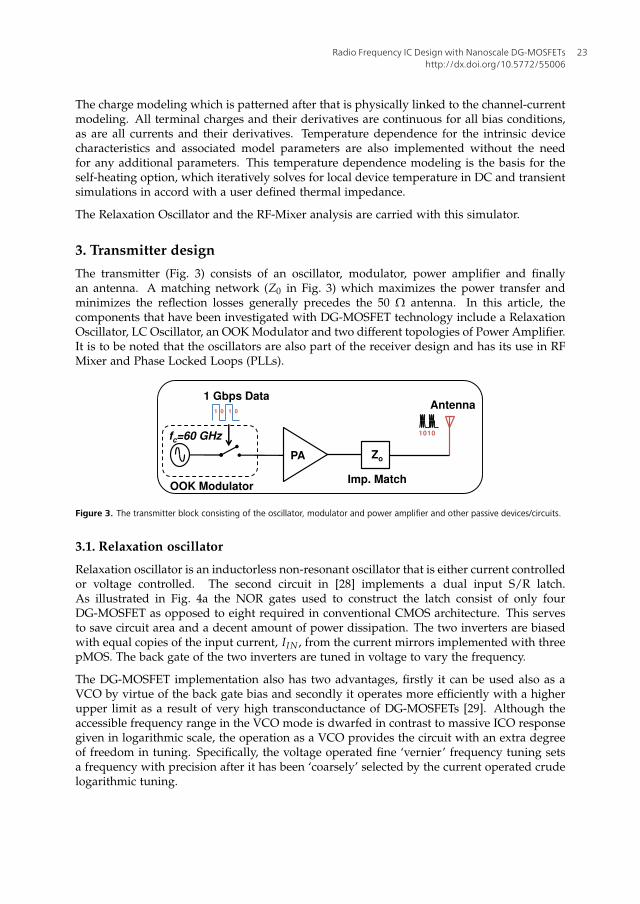
3. Transmitter design
The transmitter (Fig. 3) consists of an oscillator, modulator, power amplifier and finallyan antenna. A matching network (Z0 in Fig. 3) which maximizes the power transfer andminimizes the reflection losses generally precedes the 50 Ω antenna. In this article, thecomponents that have been investigated with DG-MOSFET technology include a RelaxationOscillator, LC Oscillator, an OOK Modulator and two different topologies of Power Amplifier.It is to be noted that the oscillators are also part of the receiver design and has its use in RFMixer and Phase Locked Loops (PLLs).
PA
fc=60 GHz
Antenna
OOK Modulator
1 0 1 0
1 Gbps Data
1010
Zo
Imp. Match
Figure 3. The transmitter block consisting of the oscillator, modulator and power amplifier and other passive devices/circuits.
3.1. Relaxation oscillator
Relaxation oscillator is an inductorless non-resonant oscillator that is either current controlledor voltage controlled. The second circuit in [28] implements a dual input S/R latch.As illustrated in Fig. 4a the NOR gates used to construct the latch consist of only fourDG-MOSFET as opposed to eight required in conventional CMOS architecture. This servesto save circuit area and a decent amount of power dissipation. The two inverters are biasedwith equal copies of the input current, IIN , from the current mirrors implemented with threepMOS. The back gate of the two inverters are tuned in voltage to vary the frequency.
The DG-MOSFET implementation also has two advantages, firstly it can be used also as aVCO by virtue of the back gate bias and secondly it operates more efficiently with a higherupper limit as a result of very high transconductance of DG-MOSFETs [29]. Although theaccessible frequency range in the VCO mode is dwarfed in contrast to massive ICO responsegiven in logarithmic scale, the operation as a VCO provides the circuit with an extra degreeof freedom in tuning. Specifically, the voltage operated fine ‘vernier’ frequency tuning setsa frequency with precision after it has been ‘coarsely’ selected by the current operated crudelogarithmic tuning.
Radio Frequency IC Design with Nanoscale DG-MOSFETshttp://dx.doi.org/10.5772/55006
23
6 Analog Circuits
VDD
VDD
Q
Vbgp
Vbgn
Q
Q
R
Vbgp
Vbgn
C
S
C
Q
VDD
VDD
VDD
IIN
(a)
0.1 1 10 1000.01
0.1
1
10
Current (µA)
Fre
qu
ency
(G
Hz)
0.6 V; 0.4 V (Single)0.8 V; 0.4 V (Single)1 V; 0.6 V (Dual)1.2 V; 0.6 V (Dual)
Figure 4. a)The current/voltage controlled relaxation oscillator in DG-MOSFET technology. b) The ‘crude tuning’ of the
relaxation oscillator with varying current. c) The fine tuning in frequency with back gate bias when Vp
bg = Vnbg of the relaxation
oscillator.
In Fig. 4b, we can verify the frequency has a log-log relationship with the current. Thefrequency ranges from 30 MHz to a few GHz for a change in current supply from 0.4 µAto 50 µA. This coarse tuning in frequency is supported via back gate fine tuning of the DGMOSFET inverters. For a constant current and voltage supply, the frequency can be tunedto vary in the order of MHz, as the inverter back gate voltage varies from 0.1 V to 1 V. Itis observed, a higher VDD results in a slower oscillation at a fixed input current, becausethe SR Latch takes longer time to reach a higher switching threshold (∼ 1/2VDD) as VDD
is increased. The Fig. 4c demonstrates these facts with three different current sources andsupply voltage. The phase noise of the oscillator is -104 dBc/Hz at 1 MHz offset. All theseanalysis are carried with 45 nm DG-MOSFET using UFDG SPICE.
Analog Circuits24
Radio Frequency IC Design with Nanoscale DG-MOSFETs 7
10.5772/55006
3.2. LC oscillator and OOK modulator
LC oscillators consists of inductors and capacitors connected in parallel. Although inductorsconsume a lot of area when compared to the inductorless oscillator described aboveoscillators, it is a must in RF Design to use inductors because of two primary reasons [30].They are as follows:
• The resonance of inductors with capacitors allow for higher operational frequency andlower phase noise.
• The inductor sustains a very small DC voltage drop which aids in low supply operation.
We have chosen the differential negative resistance voltage controlled oscillator (VCO) variantof the LC oscillator (Fig. 5a) for the investigation. The latch circuit in the differential modeserves as negative resistance to nullify the effects of a positive resistance arising out ofthe imperfect inductor. The Q factor determines the undesired resistance value (R) of theinductor (L) at the resonance frequency, ω. Modeling the resistive loss in the inductor, L bythe parallel resistance (R) we can write [30]:
Q =R
ωL(1)
The LC tank achieves a frequency that is much higher and has a phase noise that is muchlower than that of the relaxation oscillator. This is primarily because of the resonance of thecircuit.
The OOK Modulation is a non-coherent modulation scheme that modulates the carrier onlywhen the circuit is in the ‘ON’ state. It is the special case of Amplitude Shift Key (ASK)modulation where no carrier is present during the transmission of a ‘zero’. The bit error ratefor OOK modulation without the implementation of any error correcting scheme is given by[31]
BER =1
2exp(
−Eb
2N0) +
1
2Q
√
Eb
N0(2)
Although, the associated bit error rate of OOK modulation is inferior to that of othercoherent modulation schemes, simple OOK modulation scheme is implemented to avoid thecomplicated carrier recovery circuit and for their ability to modulate very high frequencysignals in extremely long-life battery operated applications. The non-coherent OOKdemodulation generally employs an envelope detector in the receiver which saves the power,area, cost and complexity since no local oscillator (LO) or carrier synchronization scheme isinvolved.
3.2.1. Design and simulation
The DG-MOSFET based VCO can be tuned from the back gate for controlling the rms voltage(Vrms). Fig. 5b illustrates this interesting tunable feature of the DG MOSFET VCO. Withoutany change in the supply, the Vrms can be controlled via back gate bias (Vbg), which can have
Radio Frequency IC Design with Nanoscale DG-MOSFETshttp://dx.doi.org/10.5772/55006
25
8 Analog Circuits
Vbg1 Vbg2
VDD
MN2 MN1
Vout1
From VCO,
(60 GHz
Carrier)
MN4
MN3
Data, 1 Gbps
Vout2 : To PA L1 L2
L3
C
VDD
VCO
OOK Modulator
(a)
0.2 0.24 0.28 0.32 0.36 0.4
−0.4
0
0.4
0.8
1.2
1.6
Time (GHz)
Vol
tage
(V
)
0.1 0.2 0.3 0.4 0.5 0.6 0.7 0.8 0.90
0.2
0.4
0.6
0.8
Am
plitu
de (
V)
0.1 0.2 0.3 0.4 0.5 0.6 0.7 0.8 0.954
56
58
60
62
Vbg
(V)
Fre
quen
cy (
GH
z)
0.9V0.6V0.3V
Vbg
(b)
102
103
104
105
106
107
108
−190
−160
−130
−100
−70
−40
−10
Frequency Offset (Hz)
Pha
se N
oise
(dB
c/H
z)
1 MHz Offset @60 GHz Carrier
(c)
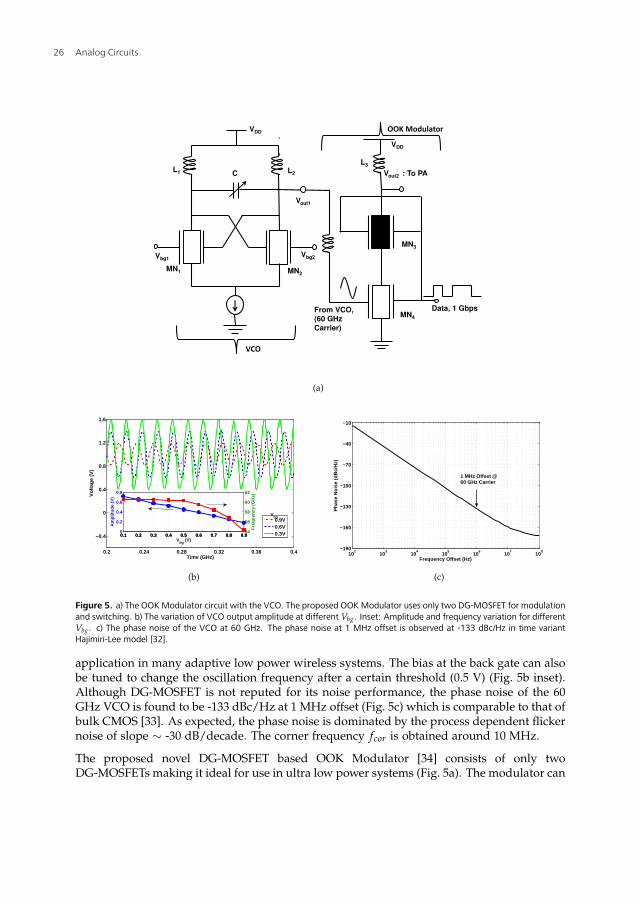
Figure 5. a) The OOKModulator circuit with the VCO. The proposed OOKModulator uses only two DG-MOSFET for modulation
and switching. b) The variation of VCO output amplitude at different Vbg. Inset: Amplitude and frequency variation for different
Vbg. c) The phase noise of the VCO at 60 GHz. The phase noise at 1 MHz offset is observed at -133 dBc/Hz in time variant
Hajimiri-Lee model [32].
application in many adaptive low power wireless systems. The bias at the back gate can alsobe tuned to change the oscillation frequency after a certain threshold (0.5 V) (Fig. 5b inset).Although DG-MOSFET is not reputed for its noise performance, the phase noise of the 60GHz VCO is found to be -133 dBc/Hz at 1 MHz offset (Fig. 5c) which is comparable to that ofbulk CMOS [33]. As expected, the phase noise is dominated by the process dependent flickernoise of slope ∼ -30 dB/decade. The corner frequency fcor is obtained around 10 MHz.
The proposed novel DG-MOSFET based OOK Modulator [34] consists of only twoDG-MOSFETs making it ideal for use in ultra low power systems (Fig. 5a). The modulator can
Analog Circuits26
Radio Frequency IC Design with Nanoscale DG-MOSFETs 9
10.5772/55006
0.5 0.6 0.7 0.8 0.9 10.5
1
1.5
Am
pli
tud
e (
V)
Career @ 60 GHz
0 0.5 1 1.5 2 2.5 3 3.5
0
0.5
1
Am
pli
tud
e (
V)
Data @ 1 Gbps
0 0.5 1 1.5 2 2.5 3 3.50
1
2
Am
pli
tud
e (
V)
Time (ns)
OOK Modulated O/P
Figure 6. The OOK Modulated output for a carrier frequency of 60 GHz and data rate of 1 Gbps. The input data sequence
resembles 50% duty cycle.
work up to a data rate of 5 Gbps without any discernible distortion for 60 GHz carrier. TheDG-MOSFET MN4 acts as the key OOK modulating device. The 60 GHz sinusoidal carrierfrom the VCO is fed into one of the gates of the transistor whereas the pulsed digital data isinput to the other gate. The charge capacitive coupling of the two gates provided by the thinSi body determines the modulation, and therefore depends on the bias conditions of the twogates as well as device dimensions. The modulation occurs when the device operates in thesaturation or in cut-off region, that is when there is either a ‘1’ or ‘0’ respectively emanatingfrom the pulsed digital data. In other words, the modulation takes place at all instants oftime. The symmetric DG-MOSFET MN3 acts as the switch and is kept at a high thresholdvoltage (filled) for better electrostatics and keying and to maximize the ION/IOFF ratio. TheMN3 is turned on at the ‘HIGH’ state of the pulsed data and remains off at the ‘LOW’ state,maintaining the principle of OOK Modulation scheme. The modulated output is obtained atthe drain of MN3. This is illustrated in Fig. 6. All these analysis are carried in 32 nm ASUPTM FinFET technology.
3.3. Power Amplifier
The Power Amplifier (PA) is the final stage of transmitter design before signal transmissionthrough antenna. They are responsible for amplifying the power level of the transmittedsignal several times so that the received signal is above the sensitivity of the receiver whichis calculated from the link budget analysis. The PAs are divided into various classes suchas A, B, AB, C D, E, F etc. Among these classes A, B, AB and C incorporate similar designmethodologies differing only in the biasing point. Among these Class A amplifier is the mostlinear and is widely used in RF transmitter design although they have the least Power AddedEfficiency (PAE). Several acclaimed literatures [35], [30] are available for interested readerson these concepts. This book chapter focusses on the design of tunable DG-MOSFET ClassA PA.
Radio Frequency IC Design with Nanoscale DG-MOSFETshttp://dx.doi.org/10.5772/55006
27
10 Analog Circuits
The design of the wide band and high gain PA is a challenging task, especially inultra-compact MOSFETs with low output impedance. Consequently, in [36], we simplyadapted two recent single-gate implementations with competitive features in the GHz range,which allows a more fair performance comparison to be made between different devices. Inthe first PA topology [37], we modify the architecture slightly for the DG-MOSFET to exploreits gain and bandwidth characteristics as well as its tunability. The second topology reportedhere is a three stage single-ended, common-source (CS) PA similar to the one reported by Yaoet al. [38] for conventional CMOS. The basic difference over the published topologies in bothcases is the length of the DG-MOSFET devices (45 nm) that is substantially smaller. Thereare a number of reasons for this gate length choice. Firstly, the proposed PAs are essentiallydesigned for low-power highly compact Si mixed-signal radio applications where the rangeand area will be typically quite limited. Secondly, the DG-MOSFET architecture is inherentlya narrow width device technology in which very large number of fingers needed to obtainlarge W/L ratios. Finally, we wish to implement a PA for ultra-compact wide-band RF CMOSapplications such as vehicular anti-collision radar. Given that DG-MOSFET technology isaimed for sub-22 nm digital technologies, 45 nm is a good compromise for analog circuitimplementation.
The next two sections will discuss in detail about these design modifications and providetheir simulated response including gain tuning, peak gain, bandwidth and linearity.Interested readers can compare the performances of these power amplifiers with a few otherconventional designs in [36].
3.3.1. Topology A - Design and simulation
The circuit topology of the first wide band (3-33 GHz) DG-MOSFET PA is shown in Fig. 7a,which consists of three DG-MOSFETs in a Darlington cascode arrangement. The commonsource transistor MN1 operates in the symmetric mode while the two transistors MN2 andMN3 are configured for independent mode operation. The width of MN1 is taken to be1 µm while the width for transistors MN2 and MN3 are kept higher at 2.4 µm for betterinput return loss and optimized gain performance. MN3 is biased at 2.6 V (Vb1). Theback gate of the transistors MN2 and MN3 are biased for gain tuning. The resistors R1
and R2 complete a self biasing network for Class A operation. This modified DG-MOSFETdarlington configuration is divided into two stages. The first stage is the series peaking stageand inter-stage matching, and the second stage is the output power stage.
The series peaking circuit consisting of R3 and L1 increases the output load pull impedance,and also provides the peaking impedance for feeding forward signals. The inductor L3 alongwith the source degeneration circuit consisting of R4 and L2 yields in real part wide bandinter-stage impedance matching for maximizing the power transfer between the stages. Thecommon source transistor MN2 and MN3 are connected in cascode. The transistor MN3 actsin common gate configuration and one of its gate is grounded with the aid of the peakinginductor L4 and a bypass capacitor C1 [30]. Along with achieving a near constant gain bymaintaining the flatness, the bandwidth of the amplifier is also increased with the aid of thispeaking inductor. A high pass L-network (L5 & C3) is used as the matching circuit.
Our simulation verifies the forward gain (S21) to vary from 3 to 33 GHz, while maintaining adesired flatness (Fig. 7b). The gain changes by less than 20% in this frequency range, attestingto the extreme flatness. The peak gain is observed at 24.5 dB. The input and output return
Analog Circuits28
Radio Frequency IC Design with Nanoscale DG-MOSFETs 11
10.5772/55006
MN1
Vbg
MN3
MN2
R1
R2
R3
R4
R5
L1
L2
L3
L4
L5
C1
C2
C3
RFout
RFin
Vb1
Vb2
(a)
0 10 20 30 40−20
−15
−10
−5
0
5
10
15
20
25
Frequency (GHz)
S p
ara
mete
rs (
dB
)
S21
S11
S22
(b)
0 10 20 30 40−30
−20
−10
0
10
20
30
Frequency (GHz)
S2
1 (
dB
)
0.1 0.15 0.2 0.2512
16
20
24
28
Vbg
(V)
S21 (
dB
)
10GHz
20GHz
30GHz0.10V
0.15V
0.20V
0.25V
Vbg
(c)
0 10 20 30 400
0.5
1
1.5
2
Frequency (GHz)
Ro
llet
Sta
bil
ity F
acto
r
(d)
Figure 7. a) The DG MOSFET based power amplifier circuit in modified darlington cascode configuration. Transistors MN1
operates in the symmetric mode while MN2 and MN3 operate in independent mode with the back gates used for dynamic
tuning. b) The S parameters which provide the gain (S21) and reflection losses (S11 & S22) of the power amplifier. This is
measured for Vbg = 0.2 V. c) The back gate dependence of the gain is clearly evident. The gain changes by ∼ 10 dB in thetuning range of Vbg. Inset: Gain variation with Vbg at different frequencies. d) The rollet stability factor (K) is above unity in
the operating range of 2 - 32 GHz verifying the amplifier to remain unconditionally stable in this range. K drops below unity
beyond ∼ 38 GHz.
losses (S11 & S22) are also obtained from the simulation. Fig. 7c shows these S parameters ata Vbg of 0.2 V which is applied at the back gate of the transistors MN2 and MN3. The backgate voltage (Vbg) is varied from 0.1 V to 0.25 V for the operating frequency range duringwhich the gain of the amplifier increases considerably. The range of gain tuning is observedto be limited to almost 10 dB. The inset of the figure shows the gain variation with Vbg atdifferent frequencies. The unconditional stability of the amplifier is verified measuring therollet stability factor, K which is given as
K =1 − |S11|
2 − |S22|2+ ||2
2|S12S21|(3)
= S11S22 − S12S21 (4)
Radio Frequency IC Design with Nanoscale DG-MOSFETshttp://dx.doi.org/10.5772/55006
29
12 Analog Circuits
VDD VDD VDD
RFout
RFin
Vbg Vbg Vbg
Vb Vb
L2
L3
L4
L7
L5
L6
L8
L9
L1
C1
C2 C
3
R1 R2
MN1 MN2 MN3
(a)
20 30 40 50 60 70 80 90 100−30
−20
−10
0
10
Frequency (GHz)
S p
ara
mete
rs (
dB
)
S21
S11
S22
(b)
40 50 60 70 80 90 100−10
−6
−2
2
6
10
S2
1 (
dB
)
Frequency (GHz)
0.2 0.3 0.4 0.50
2
4
6
8
10
Back gate Bias (V)
S2
1 (
dB
)
55GHz75GHz95GHz
0.2V0.3V0.35V0.4V0.45V0.5V
Vbg
(c)
50 60 70 80 90 1001
3
5
7
Frequency (GHz)
Ro
llet
Sta
bil
ity F
acto
r
(d)
Figure 8. a) The three stage DG MOSFET based power amplifier circuit. All the three transistors operate in the independent
mode. b) The S parameters which provide the gain (S21) and reflection losses (S11 & S22) of the power amplifier. This is also
measured for Vbg = 0.2 V. c) The back gate dependence of the gain is clearly evident. The gain changes by ∼ 6 dB in the tuning
range of Vbg. Inset: Gain variation with Vbg at different frequencies. d) The rollet stability factor (K) is well over unity in the
operating range of 60 - 90 GHz verifying the amplifier to remain unconditionally stable in the range.
The value of K is observed to be above unity in the operating frequency range indicating theunconditional stability of the amplifier (Fig. 7d). The back gate tuning of the PA is verifiedfrom Fig. 5. The 1 dB compression point (P1dB) and the 3rd order Input Intercept Point (IIP3)are found to be 11.9 dBm and 27.5 dBm, respectively, indicating the suitability of the circuit.The 15.6 dB difference between P1dB and IIP3 can be attributed to the scaling down of DGMOSFET to 45 nm [35]. The power added efficiency (PAE) and the fractional bandwidth (FB)of the amplifier is ∼12% and 176% respectively.
3.3.2. Topology B - Design and simulation
In the second topology, the DG-MOSFET Class A amplifier is implemented in three stages(Fig. 8a). Although the earlier cascode topology has higher & flatter gain, and larger outputimpedance, the CS configuration is advantageous in terms of the lower supply voltagerequired, leading to higher efficiency. All the transistors in this topology operate in the
Analog Circuits30
Radio Frequency IC Design with Nanoscale DG-MOSFETs 13
10.5772/55006
LNA
Antenna
RF Front End Demodulator
1010
Local Oscillator
Mixer
Envelope
Detector/PLL
IF
Zo
Imp.
Match
1 0 1 0
Received Data
Figure 9. The receiver block consisting of the RF Front End (LNA & RF Mixer) and the Demodulator (Envelope Detector, for
non-coherent detection or PLL, for coherent detection).
independent mode. The source degeneration inductors L3, L6 and L9 along with the interstage inductors L4 and L7 maximizes the power transfer and improves linearity [35]. Thewidth of the three transistors are kept fixed at 1.2 µm. The source and the bias voltage (Vb)are both kept at 1 V.
Although the 3-dB bandwidth is ≥ 50 GHz, as evident from Fig. 8b, for all cases of back gatevoltages (Fig. 8c) a more realistic operating range of this amplifier can be considered to bein the range of 60 - 90 GHz. Once again, the inset of the Fig. 8 shows the gain variationwith Vbg at different frequencies. The peak gain achieved is ≥ 8 dB. The rollet stability factorremains more than unity for this operating range as shown by simulated data in Fig. 8d. TheP1dB and the IIP3 are found to be 7.2 dBm and 19.8 dBm respectively. The PAE and the FB ofthis amplifier is ∼14% and 40% respectively.
4. Receiver design
The front end of the receiver consists of a Low Noise Amplifier (LNA) and RF Mixer. Todemodulate a non-coherent signal an Envelope Detector is used while to demodulate acoherent signal a Phase Locked Loop is generally used (Fig. 9). In this chapter, we havedesigned an LNA, Envelope Detector and a Charge Pump Phase Frequency Detector (whichis an essential component in PLL design) and analyzed an existing RF Mixer.
4.1. Low Noise Amplifier
The Low Noise Amplifier (LNA) is an essential component in the front-end of anycommunication/navigation receiver. The received signal at antenna is very weak andtherefore it is necessary to amplify the signal for demodulation and processing. At the sametime the noise figure of the amplifier has to be very low because the received signal willeventually be passed to non-linear devices such as RF Mixers which add noise. ThereforeLNA design optimizes to minimize the noise level at the first stage of the receiver i.e. at theLNA itself. Other characteristics that require from an LNA include high gain, impedancematching linearity and stability.
The circuit topology of the tunable 45 nm DG-MOSFET LNA implemented here is shownin Fig. 10, which consists of three DG-MOSFETs in a 2 stage common source cascodetopology. The common source transistor MN1 operates in the symmetric mode while the twotransistors MN2 and MN3 are configured for independent mode operation. The common
Radio Frequency IC Design with Nanoscale DG-MOSFETshttp://dx.doi.org/10.5772/55006
31
14 Analog Circuits
RFin
Vbg
L2
L3
L4
L5
L1
C1
C2
MN1
MN2
MN3
RFout
Vb
R1
VDD
Figure 10. The DG MOSFET based LNA in common source cascode configuration. Transistors MN1 operates in the symmetric
mode while MN2 and MN3 operate in the independent mode with the back gates used for dynamic tuning.
40 50 60 70 80
−40
−20
0
20
10
−10
−30
−50
Frequency (GHz)
S21
(dB
)
0.30.40.50.60.7
Vbg
(V)
(a)
20 30 40 50 60 70 80 900
4
8
12
16
Frequency (GHz)
Noi
se F
igur
e (d
B)
0.70.60.50.40.3
Vbg
(V)
(b)
Figure 11. a) The gain (S21) of the LNA varies with Vbg. This is measured for Vbg = 0.3 V to 0.7 V. b) The noise figure
dependence on Vbg of the LNA is evident. The NF changes by 4.4 dB in the tuning range of Vbg at 65 GHz.
source transistor MN2 and MN3 are connected in cascode. The transistor MN3 acts incommon gate configuration. The width of MN1 is taken to be 1 µm while the width fortransistors MN2 and MN3 are kept higher at 2.4 µm for better input return loss and optimizedgain performance. The supply, VDD is kept constant at 1.2 V. MN3 is biased at 2 V (Vb). Theback gate of the transistors MN2 and MN3 are biased for gain tuning.
The series peaking circuit consists of an inductive load, L2, that allows for low voltageoperation and resonates with the inter stage capacitance, C1, enabling a higher operatingfrequency [30]. The inductor L1 is set to resonate with the gate source capacitance of MN1.The source degeneration circuit consisting of L3 yields (in real part) wide band impedancematching to maximize the inter-stage power transfer. The inductor L4 tunes out the middlepole of the cascode, thus compensating for the lower fT [39] of DG-MOSFET which is nearly150 GHz at 45 nm.
Analog Circuits32
Radio Frequency IC Design with Nanoscale DG-MOSFETs 15
10.5772/55006
The simulation shows the 3-dB bandwidth to be 15 GHz, ranging from 60 to 75 GHz. Theforward gain (S21) achieves a peak value of 15 dB at 65 GHz for Vbg = 0.7 V (Fig. 11a).Beyond this maximum operating voltage the gain gets saturated and is independent of Vbg.The peak gain reduces gradually as Vbg is reduced and drops to ∼5 dB for Vbg = 0.3 V. Thepower dissipated (Pdc) by the LNA also varies with Vbg, reaching 18 mW at Vbg = 0.7 V.Similarly, the LNA noise figure (NF) also depends upon the back gate bias, dropping to aminimum at peak gain as expected. It ranges from 7 dB at Vbg = 0.7 V to 11.4 dB at Vbg =0.3 V (Fig. 11b). Clearly, the back gate tuning provides a convenient tool to optimize specificdevice performance parameters, setting up unique trade-offs such as that between power andgain.
The proposed LNA is unconditionally stable in the operating frequency range, verified fromthe simulated rollet stability factor, i.e. K > 1. The circuit is also simulated for linearityperformance using a two tone frequency analysis near 60 GHz and the observed 3rd orderInput Intercept Point (IIP3) is −5.2 dBm.
Overall, the DG-MOSFET implementations have impressive characteristics that either matchor exceed the bulk MOSFET and even SiGe counterparts [40]-[42]. It is fair to point outthat much of this response can be attributed to small gate length in our designs. However,a short gate length has also consequences for linearity and lower output impedance, withwhich this architecture appears to cope well.
4.2. RF mixers
The RF mixer is a non-linear electrical circuit that creates two new frequencies from the twosignals applied to it. The new frequencies (sum & difference) are called the intermediatefrequencies (IF). The sum frequency has its application on the up conversion whereas thedifference frequency is used in the down conversion of an input signal. The conversion gain(CG) determines the mixing performance of the circuit [35].
4.2.1. DG-MOSFET mixers and methodology
DG-MOSFET mixer occupies a special status among analog applications given the compactand high performance nature of an active mixer using only one transistor which saves bothpower and area compared to conventional CMOS. Accordingly, there are already severalliteratures available focusing solely on this simple but promising circuit. For instance, arecent work by S. Huang et. al. [43] analyzes the RF Mixer based on the derivativesuperposition method. An earlier work [44] considers the evaluation of power consumptionand area overhead of the DG-MOSFET for RF-mixer applications. W. Zhang et. al. [45]explored the use of multiple independent-gate FinFETs (MIGFETs) application and comparesthe spectral response of the single-and multiple-transistor (balanced) versions. Althoughthis research provides valuable physical insights regarding the operational principles andbehavior of the DG-MOSFET mixer, unfortunately the temporal resolution or the length ofthe transient data used in their Fast Fourier Transform (FFT) analysis, and the range of deviceparameters explored, are insufficient for a thorough study of the mixing performance in amethodical manner.
In contrast, in [46] we focus on the structural and operational parameters of DG-MOSFETin a methodical and accurate manner to optimize the biasing for maximum conversion
Radio Frequency IC Design with Nanoscale DG-MOSFETshttp://dx.doi.org/10.5772/55006
33
16 Analog Circuits
vLO
vRF
VDD
ID
ID/2 ID/2
RL
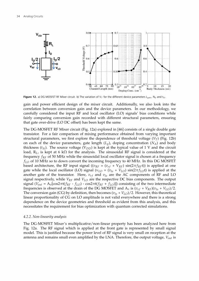
Figure 12. a) DG MOSFET RF Mixer circuit. b) The variation of VT for the different device parameters Lgate, Nd and tSi .
gain and power efficient design of the mixer circuit. Additionally, we also look into thecorrelation between conversion gain and the device parameters. In our methodology, wecarefully considered the input RF and local oscillator (LO) signals’ bias conditions whilefairly comparing conversion gain recorded with different structural parameters, ensuringthat gate over-drive (LO DC offset) has been kept the same.
The DG-MOSFET RF Mixer circuit (Fig. 12a) explored in [46] consists of a single double gatetransistor. For a fair comparison of mixing performance obtained from varying importantstructural parameters, we first explore the dependence of threshold voltage (VT) (Fig. 12b)on each of the device parameters, gate length (Lg), doping concentration (NA) and bodythickness (tSi). The source voltage (VDD) is kept at the typical value of 1 V and the circuitload, RL, is kept at 6 kΩ for the analysis. The sinusoidal RF signal is considered at thefrequency fRF of 50 MHz while the sinusoidal local oscillator signal is chosen at a frequencyfLO of 10 MHz so to down convert the incoming frequency to 40 MHz. In this DG MOSFETbased architecture, the RF input signal ((vRF = (vr f + VRF) sin(2π fRFt)) is applied at onegate while the local oscillator (LO) signal (vLO = (vlo + VLO) sin(2π fLOt) is applied at theanother gate of the transistor. Here, vr f and vlo are the AC components of RF and LOsignal respectively, while VRF and VLO are the respective DC bias components. The outputsignal (Vout = Av[cos2πt( fRF - fLO) - cos2πt( fRF + fLO)]) consisting of the two intermediatefrequencies is observed at the drain of the DG MOSFET and Av is (vr f + VRF)(vlo + VLO)/2.The conversion gain (CG) by definition, then becomes (vlo + VLO)/2. However, this theoreticallinear proportionality of CG on LO amplitude is not valid everywhere and there is a strongdependence on the device geometries and threshold as evident from this analysis, and thisnecessitates the requirement for bias optimization with quantum corrected simulations.
4.2.2. Non-linearity analysis
The DG-MOSFET Mixer’s multiplicative/non-linear property has been analyzed here fromFig. 12a. The RF signal which is applied at the front gate is represented by small signalmodel. This is justified because the power level of RF signal is very small on reception at theantenna and remains small even amplified by the LNA. Therefore, the output voltage, Vout is
Analog Circuits34
Radio Frequency IC Design with Nanoscale DG-MOSFETs 17
10.5772/55006
given as:
Vout = gmvRFRL (5)
where gm is the transconductance of the device at the front gate. The I-V characteristics ofDG-MOSFET at saturation is modeled as [47]
ID = K[(Vgs − VT)2− K′e
Vgs−V0−VdskT ] (6)
where K & K’ are process and device constants and V0 is a second order term of VT [47]. Herethe drain current at the front gate is modeled by ignoring the exponential term assuming alarge Vds at saturation, where the numerator at the exponent goes negative.
ID
2≃ K(Vgs − VT)
2 (7)
The transconductance at the front gate is,
gm =1
2
∂ID
∂Vgs(8)
From eqns. (7) and (8) we can write,
gm = 2K(Vgs − VT) (9)
Now from eqns. (7) and (9),
gm =√
(2KID) (10)
A large signal model is assumed for the back gate as the LO signal is locally generated andusually has high amplitude levels,
ID/2 = K(vLO − VT)2 (11)
implies,
ID = 2K(vLO − VT)2 (12)
Radio Frequency IC Design with Nanoscale DG-MOSFETshttp://dx.doi.org/10.5772/55006
35
18 Analog Circuits
Therefore from eqns. (5), (10) & (12),
Vout = K′′(vLO − VT)vRF (13)
Here K′′ is a constant which include the process and device parameters and the resistor RL.The eqn. (13) analyzes the DG-MOSFET device analysis for non-linear RF Mixer operation.The output voltage is the product of two input voltages. The process dependent parameterVT can be eliminated if we consider a balanced/differential mixer mode. However, typicallythe balanced mode is avoided because in a receiver design the mixer follows the LNA whichis generally single ended as it follows a single ended antenna. A balun which consumes alarge area is thus required to construct before the mixer for the differential mode use.
4.2.3. Operating point analysis
After the FFT analysis (Fig. 13a inset) of the output at a very high temporal resolution,we observe significant spectral lines at the two intermediate frequencies of 40 MHz ( fRF -fLO) and 60 MHz ( fRF + fLO) indicating the appropriate double gate mixing performanceand non-linearity. The presence of higher harmonics (such as at 100 MHz frequency) inthe spectra indicates higher-order non-linearities and must be filtered out to work with thedesired frequency. For the analysis purposes and simplification of the observed spectra, theLO signal used in our study is a pure sine-wave with a DC offset providing the operatingpoint for the device, while the RF AC input at the another gate is held constant without aDC offset.
Our study indicates that the CG of the mixer rapidly changes with the amplitude of theLO rising to 200 mV (Fig. 13b), beyond which the increase is limited. Hence, for all Lgate
values, the operating point of the mixer is chosen to be set around 120 mV for optimumpower efficiency and CG. Similar results were also obtained for different NAs and tSis fromcorresponding analyses.
The CG is particularly sensitive to the LO DC bias (Fig. 13c) with an ‘m-shape’ dependence,where the middle dip could be as much as -80 dB. Hence, seemingly there are two biasconditions that provide similar performance in CG of the mixer (Fig. 13b). For instance,these two bias points are observed at 0.3 V and 1 V for Lgate = 30 nm and vlo = 40 mV.Moreover, this m-shape is a very weak function of LO AC bias and Lgate. Data recordedwith AC inputs of 40 mV with 120 mV shift mainly vertically with a large lateral similarityin terms of DC bias dependence. Likewise, the peak position shifts roughly 0.1 V only, asthe gate length is varied from 90 nm to 30 nm. It is interesting to note that these optimumDC-bias ranges correspond to the least ‘linear’ sections of the device operation, as can beseen from the transfer characteristics and transconductance (gm vs. Id) curves in Fig. 13d.The current changes in a very non linear pattern around the optimum bias ranges and thegm peak corresponds to the central dip in Fig. 13c. Clearly, the lower bias point (∼ 0.3 Vin Fig. 13c) should be preferred because of power efficiency and better stability indicated bythe broader plateau. Similar analyses conducted for different NA and tSi of the DG-MOSFETmixer yield in similar results to our study of Lgate. A double-peaked LO-DC behavior persistsin all cases. Summarizing results from these simulations, Tables 1, 2 and 3 list the optimum(lower) bias points for different structural parameters studied.
Analog Circuits36
Radio Frequency IC Design with Nanoscale DG-MOSFETs 19
10.5772/55006
(a)
0 50 100 150 200 250 300 350 400 450 500−25
−20
−15
−10
−5
0
5
10
AC Input (mV)
Con
vers
ion
Gai
n (d
B)
30nm45nm90nm
Lgate
(b)
0 0.2 0.4 0.6 0.8 1 1.2 1.4−160
−140
−120
−100
−80
−60
−40
−20
0
LO DC Bias (V)
Con
vers
ion
Gai
n (d
B)
30nm50nm70nm90nm
Lgate
VAC
= 40mV
VAC
= 120mV
(c)
0 0.2 0.4 0.6 0.8 1 1.20
0.1
0.2
0.3
LO DC Bias (V)
gm
(m
S)
or I
d (
mA
)
0.2 0.3 0.4 0.5 0.60
0.5
1
1.5
2
gm
(µ
S)
30nm50nm70nm90nm
Lgate
Optimum DC Biaspoints for DG Mixer
Id
gm
(d)
Figure 13. a) The FFT (inset) of the voltage at the mixer output (main panel) shows both the sum & difference terms as well as
additional higher order harmonics. b) Variation of conversion gain with AC Input for different Lgates. The CG increases rapidly
before 120mV, after which the performance of the conversion gain is limited. c) Variation of CG with DC bias at different Lgates.
Observation of two AC inputs (120 mV & 40 mV) shows their CG variation with DC bias is similar. d) Transconductance (gm) &
drain current (Id) over DC bias for different Lgates. Out of two optimum bias points, the lower one at 0.3 V (30 nm) is chosen
for better stability and power efficiency.
Lgate (nm) 30 50 70 90
DC Bias (V) 0.30 0.41 0.45 0.47
Table 1. Optimum LO DC bias for different gate lengths at NA = 1015 cm−3 & tSi = 5 nm
NA (cm−3) 1015 1016 1017 1018
DC Bias (V) 0.45 0.47 0.48 0.50
Table 2. Optimum LO DC bias for different doping concentrations at Lgate = 45 nm & tSi = 5 nm
Radio Frequency IC Design with Nanoscale DG-MOSFETshttp://dx.doi.org/10.5772/55006
37
20 Analog Circuits
tSi (nm) 5 10 20 30
DC Bias (V) 0.6 0.5 0.4 0.3
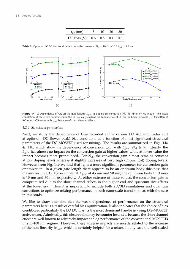
Table 3. Optimum LO DC bias for different body thicknesses at NA = 1015 cm−3 & Lgate = 90 nm
30 40 50 60 70−25
−20
−15
−10
−5
0
5
Gate Length (nm)
Con
vers
ion
Gai
n (d
B)
40mV80mV200mV
1015
1016
1017
1018
−25
−20
−15
−10
−5
0
5
Doping Concentration (cm −3)
40mV80mV200mV
VACV
AC
(a)
0 10 20 30 40 50 60−16
−12
−8
−4
0
4
Body Thickness (nm)C
onve
rsio
n G
ain
(dB
)
80mV(Lgate
=45nm)
80mV(Lgate
=90nm)
200mV(Lgate
=45nm)
200mV(Lgate
=90nm)
VAC
(b)
Figure 14. a) Dependence of CG on the gate length (Lgate) & doping concentration (NA) for different AC Inputs. The weak
correlation of these two parameters on the CG is clearly evident. b) Dependence of CG on the body thickness (tSi ) for different
AC Inputs. CG varies with Lgate because of short channel effects.
4.2.4. Structural parameters
Next, we study the dependence of CGs recorded at the various LO AC amplitudes andat optimum DC (lower peak) bias conditions as a function of most significant structuralparameters of the DG-MOSFET used for mixing. The results are summarized in Figs. 14a& 14b, which show the dependence of conversion gain with Lgate, NA & tSi. Clearly, theLgate has almost no impact on the conversion gain at higher values while at lower value theimpact becomes more pronounced. For NA, the conversion gain almost remains constantat low doping levels whereas it slightly increases at very high (impractical) doping levels.However, from Fig. 14b we find that tSi is a more significant parameter for conversion gainoptimization. In a given gate length there appears to be an optimum body thickness thatmaximizes the CG. For example, at Lgate of 45 nm and 90 nm, the optimum body thicknessis 10 nm and 30 nm, respectively. At either extreme of these values, the conversion gate iscompromised due to the short channel effects in the higher end and quantum size effectsat the lower end. Thus it is important to include both 2D/3D simulations and quantumcorrections to optimize mixing performance in such nano-scale transistors, as with the casein this study.
We like to draw attention that the weak dependence of performance on the structuralparameters here is a result of careful bias optimization. It also indicates that the choice of biasconditions, particularly the LO DC bias, is the most dominant handle in using DG-MOSFETactive mixer. Admittedly, this observation may be counter intuitive, because the short channeleffect are well known to adversely impact analog performance of the conventional MOSFETsin sub-100 nm regime. However, these adverse impacts are mostly related to the increaseof the non-linearity in gm which is certainly helpful for a mixer. In any case the well-scaled
Analog Circuits38
Radio Frequency IC Design with Nanoscale DG-MOSFETs 21
10.5772/55006
0.9 0.95 1 1.05 1.1−90
−70
−50
−30
−10
Frequency (GHz)
Pou
t (dB
m)
IMR = 36dB
Fundamental Tones: f1 & f
2
IP3 Terms: 2f
1 − f
2, 2f
2 − f
1
Figure 15. Computation of IP3 using two tone frequency analysis (0.99 GHz and 1.01 GHz) around 1 GHz. The Intermodulation
Ratio (IMR) gives level difference between the fundamental and the IP3 terms and is used to obtain the IIP3 = Pin(f1,f2) + IMR/2.
nature of the DG-MOSFET minimizes the emergence of strong short channel effects for themixer performance.
Moreover, the apparent stability of mixer performance with device geometrical scaling couldaffect the phase noise in both positive and negative fashion. In terms of inter-deviceperformance variations, the DG-MOSFETs will not suffer as much as the logic applications asthe process variations in geometry does not appear to be a worry. However, since the LO-DCbias is the most important figure of merit, variations in threshold among devices and biasingerrors/variations in circuits can be the main source of phase noise and limit the performance.
4.2.5. Linearity analysis
Finally, we examine the circuit for linearity implementing the two tone frequency analysis(Fig. 15). The 3rd order Input Intercept point (IIP3) is found to be 15.9 dBm for 2 dBm LOpower, indicating the suitability of the circuit [35].
4.3. Envelope detector
The demodulation of a non-coherent modulated wave requires an envelope detector. Theenvelope detector is basically a rectifier circuit that generates an envelope of the incominghigh frequency carrier signal and strips off the carrier to recover the data.
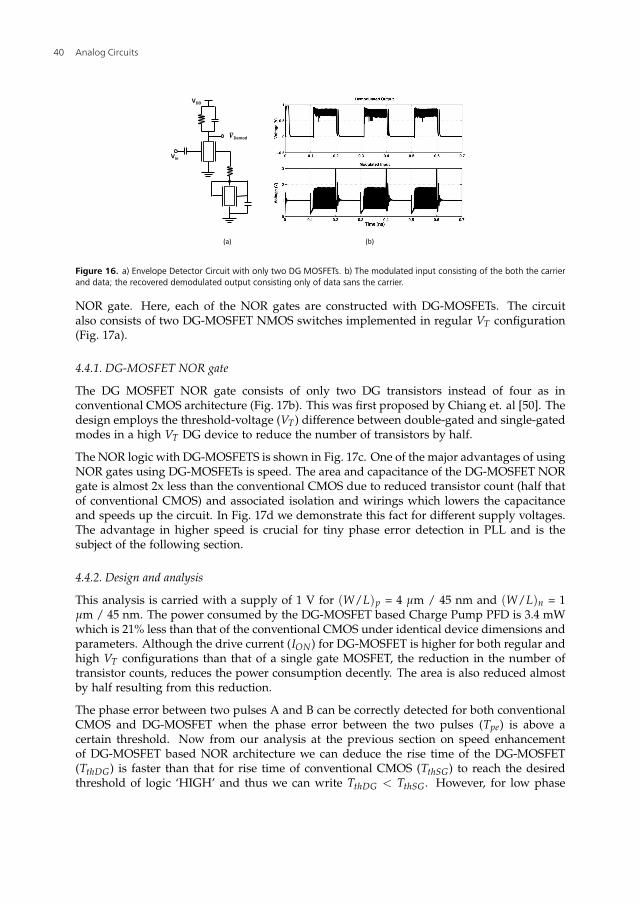
In Fig. 16a, we have illustrated a 45 nm DG-MOSFET envelope detector circuit in which theoutput is inverted to that of binary input (Refer Fig. 6). The output signal needs furtherto be passed through an inverter for the recovery of the original signal. Although requiresadditional hardware, this circuit has an advantage over the straightforward recovery as theformer has a better output swing over the latter [48]. The simulation (Fig. 16b) illustrates therecovered binary input information as same as that is shown in Fig. 6. The high frequencynoise present with logic 1 data at the output can be easily filtered out.
4.4. Charge pump Phase Frequency Detector
The Phase Frequency Detector (PFD) is one of the two major components of a PLL, thatis used for the demodulation of coherent modulated signal. The other being the localoscillator/VCO. It consists of two D Flip Flops and a reset circuit. The two D Flip Flopsare implemented with eight NOR gates (four each) [49]. The reset path consists of another
Radio Frequency IC Design with Nanoscale DG-MOSFETshttp://dx.doi.org/10.5772/55006
39
22 Analog Circuits
Demod
Vin
VDD
(a) (b)
Figure 16. a) Envelope Detector Circuit with only two DG MOSFETs. b) The modulated input consisting of the both the carrier
and data; the recovered demodulated output consisting only of data sans the carrier.
NOR gate. Here, each of the NOR gates are constructed with DG-MOSFETs. The circuitalso consists of two DG-MOSFET NMOS switches implemented in regular VT configuration(Fig. 17a).
4.4.1. DG-MOSFET NOR gate
The DG MOSFET NOR gate consists of only two DG transistors instead of four as inconventional CMOS architecture (Fig. 17b). This was first proposed by Chiang et. al [50]. Thedesign employs the threshold-voltage (VT) difference between double-gated and single-gatedmodes in a high VT DG device to reduce the number of transistors by half.
The NOR logic with DG-MOSFETS is shown in Fig. 17c. One of the major advantages of usingNOR gates using DG-MOSFETs is speed. The area and capacitance of the DG-MOSFET NORgate is almost 2x less than the conventional CMOS due to reduced transistor count (half thatof conventional CMOS) and associated isolation and wirings which lowers the capacitanceand speeds up the circuit. In Fig. 17d we demonstrate this fact for different supply voltages.The advantage in higher speed is crucial for tiny phase error detection in PLL and is thesubject of the following section.
4.4.2. Design and analysis
This analysis is carried with a supply of 1 V for (W/L)p = 4 µm / 45 nm and (W/L)n = 1µm / 45 nm. The power consumed by the DG-MOSFET based Charge Pump PFD is 3.4 mWwhich is 21% less than that of the conventional CMOS under identical device dimensions andparameters. Although the drive current (ION) for DG-MOSFET is higher for both regular andhigh VT configurations than that of a single gate MOSFET, the reduction in the number oftransistor counts, reduces the power consumption decently. The area is also reduced almostby half resulting from this reduction.
The phase error between two pulses A and B can be correctly detected for both conventionalCMOS and DG-MOSFET when the phase error between the two pulses (Tpe) is above acertain threshold. Now from our analysis at the previous section on speed enhancementof DG-MOSFET based NOR architecture we can deduce the rise time of the DG-MOSFET(TthDG) is faster than that for rise time of conventional CMOS (TthSG) to reach the desiredthreshold of logic ‘HIGH’ and thus we can write TthDG < TthSG. However, for low phase
Analog Circuits40
Radio Frequency IC Design with Nanoscale DG-MOSFETs 23
10.5772/55006
QA
QB
QA
QB
D
A
B
Vout
CP
D
MN1
MN2
I1
I2
(a)
Vout
Vdd
VB
VA
Vdd
VA
VA VB
Vout
VB
(b)
0
1
VA
(V
)
0
1
VB
(V
)
0 20 40 60 80 100 120 140 160 180 200
0
1
Time (ns)
Vo
ut (
V)
(c)
0.6 0.7 0.8 0.9 10.48
0.52
0.56
0.6
0.64
0.68
VDD
(V)
De
lay
(ps)
DG−MOSFETConventional CMOS
(d)
Figure 17. a) The Charge Pump PFD circuit implemented with DG-MOSFETs. b) 2-Input NOR Logic Gate in Conventional CMOS
and its equivalent in DG-MOSFET. Two transistors are required in the DG-MOSFET. The PMOS in DG-MOSFET is kept at a high-VT
symbolized by a filled transistor. c) 2-Input DG-MOSFET NOR Logic simulated waveform for VDD = 1 V. d) Delay comparison of
2-input NOR gate between conventional CMOS and DG-MOSFET for different supply voltages.
error applications, when TthDG ≤ Tpe ≤ TthSG, the PFD ceases to work correctly for theconventional CMOS. As observed from Fig. 18, for Tpe = 80 ps, the voltage at the outputQA of the flip flop fails to reach the threshold to switch on the transistor MN1 in the periodwhen A is ‘HIGH’ and B is ‘LOW’. The voltage only reaches the threshold when both A andB are HIGH. When B is high the voltage at QB also reaches ‘HIGH’ which turns the transistorMN2 ‘ON’. Therefore, when both QA and QB are ‘HIGH’ (reaches the VT) simultaneously,the current I1 instead of charging the capacitor CP passes through the switch MN2. Thus theoutput voltage (Vout) remains nearly constant and changes only by a fraction of what shouldbe in order to send the accurate message of phase error to the VCO, which follows the PFDin a PLL architecture. As a matter of fact, the Vout changes only by a meagre 0.005 mV for100 ns. This is negligible and an incorrect feedback to the VCO. The Vout characteristics isverified from Fig. 19. This is the familiar dead zone condition where there is no or negligiblecharge pump current that contributes to no change in Vout.
Radio Frequency IC Design with Nanoscale DG-MOSFETshttp://dx.doi.org/10.5772/55006
41
24 Analog Circuits
0
1
A (
V)
0
1
B (
V)
0
1
QA
(V
)
0
1
QB
(V
)
0
11
QA
(V
)
19.4 19.6 19.8 20 20.2 20.4 20.6 20.80
1
Time (ns)
QB
(V
)
Tpe
CMOS
CMOS
DG MOSFET
DG MOSFET
TthSG
TthDG
Figure 18. Phase error characteristics of two pulses A & B for conventional CMOS and DG-MOSFET for a phase error of 80 ps.
42.22
42.222
42.224
42.226
42.228
42.23
Vo
ut (
mV
) [C
MO
S]
0 20 40 60 80 10065.4
65.6
65.8
66
66.2
Time (ns)
Vo
ut (
mV
) [D
G M
OS
]
Figure 19. Charge Pump output voltage characteristics of Conventional CMOS and DG-MOSFET when TthDG ≤ Tpe ≤ TthSG
On the other hand, the advantage of DG-MOSFET is clearly evident from Fig. 18 where itcan be confirmed that for the same period the threshold for the DG-MOSFET reaches thelogic ‘HIGH’ when A is ‘HIGH’ and B is ‘LOW’. Thus the current I1 cannot escape throughMN2 and charges CP instead. This is clearly because even when Tpe ≤ TthSG, the inequalityTpe ≥ TthDG, is still valid due to the fact that TthDG < TthSG owing to the lower capacitanceas discussed in the previous section. Thus the dead zone is avoided with the correct andsignificant change of 0.6 mV in Vout for the same duration as that of conventional CMOS(Fig. 19).
5. Summary and future prospects
The chapter has provided examples for unique and significant performance improvementsavailable via a novel transistor architecture (FinFET or DG-MOSFET) in a wide collectionof analog and mixed-signal circuits that can be used in today’s integrated wirelesscommunication, satellite navigation systems and sensor networks, verified through industry
Analog Circuits42
Radio Frequency IC Design with Nanoscale DG-MOSFETs 25
10.5772/55006
standard SPICE simulations. In particular, the chapter documents the tunable frequencyresponse in relaxation and LC oscillators along with the gain tuning in wide-band PA and theLNA circuits. In all these cases, the performance improvements and tunable characteristicscan be achieved via the availability of independently biased second gates in these new devicearchitectures. In addition to gain tuning, the PA and the LNA performance parameters suchas gain, bandwidth, linearity, NF are either comparable or better than some of the recentdesigns in conventional CMOS or III-V technologies. The fact that DG-MOSFET circuitsutilize reduced transistor count compared to single gate CMOS is exemplified by relaxationoscillator, RF Mixer, OOK Modulator, Envelope Detector and Charge Pump PFD circuits. Asobvious, the reduced transistor count aids in reducing area and may lower power dissipation.The biasing optimization technique of the RF Mixer described here maximizes the conversiongain of the RF Mixer with power efficiency. The DG-MOSFET Charge Pump PFD circuitavoids dead zone in PLL for low phase difference applications which is not possible inconventional CMOS as demonstrated here. The primary reason for this is reduced delaybecause of reduced area which in turn is achieved as a result of reduced transistor count.
With fabrication processes of DG-MOSFETs soon coming up with initiation from TSMC andrapidly expanding system-level efforts led by several national and international programs inUS, Japan and Europe, along with several companies (such as Intel [4]) and academic centersfocussing on these DG-MOSFET/FinFET/3DMOSFET technologies, we should expect a widerange of tunable analog RF circuits, reconfigurable logic blocks, on-chip power managementblocks and mixed-signal system-on-chip applications to come into existence in the next fewyears.
Ultimately, with the ongoing nanotechnology revolution further performance improvementsand architectural changes in devices are to be expected in the next decade and beyond. Ourwork here shows that such changes can be utilized by circuit engineering to result in verycompact and capable systems, even when the actual change is to include merely an additionalgate in the MOSFET architecture. This indicates that circuit engineering has a lot more tosay not only in the final stretch of Moore’s scaling, extending perhaps until 2020, but also inpost-Moore area where fundamental fabric of building circuits may be altered significantly,and novel devices architectures and materials such as graphene, carbon nanotube, nanowireor molecular transistors are likely to play a significant role.
Acknowledgement
This research was partially supported by the NSF Award ECCS-1129010. We are thankful tothe Co-PIs of this award, Prof. Avinash Kodi of Ohio University and Prof. David Matolak ofUniversity of South Carolina (formerly of Ohio University) for their support.
School of Electrical Engineering & Computer Science, Ohio University, Athens, OH, USA
Radio Frequency IC Design with Nanoscale DG-MOSFETshttp://dx.doi.org/10.5772/55006
43
26 Analog Circuits
References
[1] G. K. Celler and Sorin Cristoloveanu. Frontiers of silicon-on-insulator. J. of AppliedPhysics, 93:4956–4978, 2003.
[2] Thomas Skotnicki, James A. Hutchby, Tsu-Jae King, H.-S.Philip Wong, and FredericBoeuf. The end of CMOS scaling. IEEE Circuits Devices Mag., pages 16–26, 2005.
[3] J. Colinge. Multi-gate SOI MOSFETs. Microelectronic Engineering (Elsevier), 84:2071–2076,2007.
[4] K. Ahmed and K. Schuegraf. Transistor Wars. IEEE Spectr., page 50, Nov 2011.
[5] Isabelle Ferain, Cynthia A. Colinge, and Jean-Pierre Colinge. Multigate transistorsas the future of classical metal-oxide-semiconductor field-effect transistors. Nature,479:310–316, Nov 2011.
[6] K. Roy, H. Mahmoodi, S. Mukhopadhyay, H. Ananthan, A. Bansal, and T. Cakici.Double-gate SOI Devices for Low-Power and High-Performance Applications. InIEEE/ACM Int. Conf. on CAD, pages 217 – 224, Nov 2005.
[7] Jae-Joon Kim and K. Roy. Double Gate-MOSFET Subthreshold Circuit for UltralowPower Applications. IEEE Trans. Electron Devices, 51:1468–1474, 2004.
[8] A. Amara and O. Rozeau (Eds.). Planar Double-Gate Transistor. Springer, 2009.
[9] S. Kaya, H.F.A Hamed, and S. Laha. Tunable Analog and Reconfigurable Digital Circuitswith Nanoscale DG-MOSFETs, chapter 9. INTECH, Rijeka, Croatia, Feb 2011.
[10] S. A. Tawfik and V. Kursun. Robust finFET memory circuits with P-Type data accessTransistors for higher Integration Density and Reduced Leakage Power. J. of Low PowerElectronics, 5:1–12, 2009.
[12] Hanpei Koike and Toshihiro Sekigawa. XDXMOS: A novel technique for theDouble-Gate MOSFETs Logic Circuits. In IEEE Custom Integrated Circuits Conference(CICC), pages 247–250, 2005.
[13] Kazuhiko Endo et. al. Four-Terminal FinFETs fabricated using an etch-back gateseparation. IEEE Trans. Nanotechnol., 6:201–205, Mar 2007.
[14] D. Wilson, R. Hayhurst, A. Oblea, S. Parke, and D. Hackler. Flexfet:Independently-double-gated SOI Transistor with Variable vt and 0.5v operationachieving near ideal subthreshold slope. In IEEE Intl. SOI Conf., pages 147–148, 2007.
[15] K. Modzelewski, R. Chintala, H. Moolamalla, S. Parke, and D.Hackler. Designof a 32nm Independently-Double-Gated flexFET SOI Transistor. In IEEEUniversity/Government/Industry Micro/Nano Symposium (UGIM), pages 64 – 67, 2008.
Analog Circuits44
Radio Frequency IC Design with Nanoscale DG-MOSFETs 27
10.5772/55006
[16] J.P Raskin, T.M. Chung, V. Kilchytska, D. Lederer, and D. Flandre. Analog/rfperformance of multiple gate SOI devices: wideband simulation and characterization.IEEE Trans. Electron Devices, 53:1088–1095, May 2006.
[17] A. Lazaro and B. Iniguez. RF and Noise performance of Double Gate and Single GateSOI. Solid State Elect., 50:826–842, 2006.
[18] B. IÃsiguez, A LÃazaro, O. Moldovan, A. Cerdeira, and T. A.Fjeldly. DC to RFSmall-Signal Compact DG MOSFET model. In NSTI-Nanotech, pages 680–685, 2006.
[19] Gen Pei and Edwin Chih-Chuan Kan. Independently driven DG MOSFETs forMixed-Signal Circuits: Part I - Quasi-Static and Nonquasi-Static Channel Coupling.IEEE Trans. Electron Devices, 51:2086–2093, Dec 2004.
[20] Xiaoping Liang and Yuan Taur. A 2-d Analytical Solution for SCEs in DG MOSFETs.IEEE Trans. Electron Devices, 51:1385–1391, Aug 2004.
[21] Huaxin Lu and Yuan Taur. An analytic Potential Model for Symmetric and AsymmetricDG MOSFETs. IEEE Trans. Electron Devices, 53:1161–1168, May 2006.
[22] Marina Reyboz, Olivier Rozeau, Thierry Poiroux, Patrick Martin, and Jalal Jomaah. Anexplicit analytical charge-based model of undoped independent double gate MOSFET.Solid State Elctronics (Elsevier), 50:1276–1282, 2006.
[23] M. Reyboz, P. Martin, T. Poiroux, and O. Rozeau. Continuous model for independentdouble gate mosfet. Solid State Elctronics (Elsevier), 53:504–513, 2009.
[24] Wei Zhao and Yu Cao. Predictive Technology Model for Nano-CMOS DesignExploration. ACM Journal on Emerging Technologies in Computing Systems, 3:1–17, 2007.
[25] J. G. Fossum. UFDG Users Guide (Ver. 3.0). University of Florida Press, Gainesville, FL,2004.
[26] L. Ge, J.G. Fossum, and B. Liu. Physical Compact Modelling and Analysis of velocityovershoot in Extremely scaled CMOS Devices and Circuits. IEEE Trans. Electron Devices,48:2074–2080, Sep 2001.
[27] K. Kim. Design and analysis of Double gate CMOS for Low Voltage Integrated CircuitApplications, including physical modeling of Silicon-on-Insulator MOSFETs. University ofFlorida Dissertation, Gainesville, FL, 2001.
[28] S. Laha, K. Wijesundara, A. Kulkarni, and S. Kaya. Ultra-compact low-power ICO/VCOcircuits with double gate MOSFETs. In IEEE International Semiconductor Device ResearchSymposium (ISDRS), pages 1–2, 2011.
[29] D. Jimenez, B. Iniguez, J. Sune, and J.J. Saenz. Analog Performance of theNanoscale Double-Gate Metal-Oxide-Semiconductor field-effect-transistor near theultimate scaling limits. Journal of Applied Physics, 96:5271 – 5276, Nov 2004.
[30] Behzad Razavi. RF Microelectronics. Prentice Hall, Boston, USA, 2012.
Radio Frequency IC Design with Nanoscale DG-MOSFETshttp://dx.doi.org/10.5772/55006
45
28 Analog Circuits
[31] F. Xiong. Digital Modulation Techniques. Artech House, Boston, 2006.
[32] A. Hajimiri and T.H. Lee. A general theory of phase noise in electrical oscillators. IEEEJ. Solid-State Circuits, 33:179–194, Feb 1998.
[33] Guansheng Li and Ehsan Afshari. A Low-Phase-Noise Multi-Phase Oscillator Based onLeft-Handed LC-Ring. IEEE J. Solid-State Circuits, 45:1822–1833, Sep 2010.
[34] S. Laha, S. Kaya, A. Kodi, and D. Matolak. 60 GHz OOK Transmitter in 32 nm DGFinFET Technology. In IEEE International Conference on Wireless Information Technologyand Systems (ICWITS) (Accepted to appear), 2012.
[35] T.H. Lee. The Design of CMOS Radio-Frequency Integrated Circuits. Cambridge UniversityPress, Cambridge, UK, 2004.
[36] S. Laha, S. Kaya, A. Kodi, and D. Matolak. Double Gate MOSFET based EfficientWideband Tunable Power Amplifiers. In IEEE Wireless and Microwave Conference(WAMICON), pages 1–4, 2012.
[37] Pin-Cheng Huang, Kun-You Lin, and Huei Wang. A 4-17 GHz Darlington CascodeBroadband Medium Power Amplifier in 0.18 micron CMOS Technology. IEEE Microw.Wireless Compon. Lett., 20:43–45, Jan 2010.
[38] Terry Yao, Michael Gordon, Kenneth Yau, M.T. Yang, and Sorin P. Voinigescu. 60-GHzPA and LNA in 90-nm RF-CMOS. In IEEE Radio Frequency Integrated Circuits (RFIC)Symposium, pages 4–7, 2006.
[39] Wong-Sun Kim, Xiaopeng Li, and M. Ismail. A 2.4 GHz CMOS low noise amplifier usingan inter-stage matching inductor. In IEEE Midwest Symposium on Circuits and Systems,pages 1040 – 1043, 2000.
[40] Michael Gordon, Terry Yao, and Sorin P. Voinigescu. 65-GHz Receiver in SiGe BiCMOSusing Monolithic Inductors and Transformers. In IEEE Topical Meeting on SiliconMonolithic Integrated Circuits on RF Systems Digest, pages 1–4, 2006.
[41] Chi-Chen Chen, Yo-Sheng Lin, Pen-Li Huang, Jin-Fa Chang, and Shey-Shi Lu.A 4.9-dB NF 53.5-62 GHz micro-machined CMOS Wideband LNA with SmallGroup-Delay-Variation. In IEEE International Microwave Symposium Digest, pages 489– 492, 2010.
[42] S. Pellarano, Y. Palaskas, and K. Soumyanath. A 64 GHz LNA with 15.5 dB Gain and6.5 dB NF in 90 nm CMOS. IEEE J. Solid-State Circuits, 43:1542–1552, Jul 2008.
[43] Shuai Huang, Xinnan Lin, Yiqun Wei, and Jin He. Derivative Superposition method forDG MOSFET application to RF mixer. In Asia Symposium on Quality Electronic Design(ASQED), page 361, 2010.
[44] M. V. R Reddy, D. K. Sharma, M. B. Patil, and V. R. Rao. Power-Area Evaluation ofVarious Double-Gate RF Mixer Topologies. IEEE Electron Device Lett., 26:664–666, 2005.
Analog Circuits46
Radio Frequency IC Design with Nanoscale DG-MOSFETs 29
10.5772/55006
[45] W. Zhang, J.G. Fossum, L. Mathew, and Y. Du. Physical Insights Regarding Design andPerformance of Independent-Gate FinFETs. IEEE Trans. Electron Devices, 52:2198–2206,2005.
[46] S. Laha, M. Lorek, and S. Kaya. Optimum Biasing and Design of High PerformanceDouble Gate MOSFET RF Mixers. In IEEE International Symposium on Circuits and Systems(ISCAS), pages 3278–3281, 2012.
[47] Y. Taur et al. A a continuous, Analytic Drain-Current model for DG MOSFETs. IEEEElectron Device Lett., 25:107–109, Feb 2004.
[48] Jri Lee, Yentso Chen, and Yenlin Huang. A Low-Power Low-Cost Fully-Integrated60-GHz Transceiver System with OOK Modulation and On-Board Antenna Assembly.IEEE J. Solid-State Circuits, 45:264–275, Feb 2010.
[49] B. Razavi. Design of Analog CMOS Integrated Circuits. McGraw Hill, Boston, USA, 2001.
[50] M.H. Chiang, K. Kim, C.T. Chuang, and C. Tretz. High-density reduced-stack logiccircuit techniques using independent-gate controlled double-gate devices. IEEE Trans.Electron Devices, 53:2370–2377, Sep 2006.
Radio Frequency IC Design with Nanoscale DG-MOSFETshttp://dx.doi.org/10.5772/55006