Micromachines 2014, 5, 622-653; doi:10.3390/mi5030622 micromachines ISSN 2072-666X www.mdpi.com/journal/micromachines Review Integrated Magnetic MEMS Relays: Status of the Technology Giuseppe Schiavone 1,2, *, Marc P. Y. Desmulliez 2 and Anthony J. Walton 1 1 Scottish Microelectronics Centre, Institute for Integrated Micro and Nano Systems, School of Engineering, The University of Edinburgh, King’s Buildings, Edinburgh EH9 3JF, UK; E-Mail: [email protected]2 Research Institute of Signals, Sensors and Systems, School of Engineering & Physical Sciences, Heriot-Watt University, Edinburgh EH14 4AS, UK; E-Mail: [email protected]* Author to whom correspondence should be addressed; E-Mail: [email protected]; Tel.: +44-131-451-8316; Fax: +44-131-451-4155. Received: 17 June 2014; in revised form: 24 July 2014 / Accepted: 19 August 2014 / Published: 29 August 2014 Abstract: The development and application of magnetic technologies employing microfabricated magnetic structures for the production of switching components has generated enormous interest in the scientific and industrial communities over the last decade. Magnetic actuation offers many benefits when compared to other schemes for microelectromechanical systems (MEMS), including the generation of forces that have higher magnitude and longer range. Magnetic actuation can be achieved using different excitation sources, which create challenges related to the integration with other technologies, such as CMOS (Complementary Metal Oxide Semiconductor), and the requirement to reduce power consumption. Novel designs and technologies are therefore sought to enable the use of magnetic switching architectures in integrated MEMS devices, without incurring excessive energy consumption. This article reviews the status of magnetic MEMS technology and presents devices recently developed by various research groups, with key focuses on integrability and effective power management, in addition to the ability to integrate the technology with other microelectronic fabrication processes. Keywords: magnetic MEMS (microelectromechanical systems); relays; MEMS integration; MEMS switches; microactuators; RF-MEMS (radio frequency MEMS) OPEN ACCESS
* Author to whom correspondence should be addressed; E-Mail: [email protected];
Tel.: +44-131-451-8316; Fax: +44-131-451-4155.
Received: 17 June 2014; in revised form: 24 July 2014 / Accepted: 19 August 2014 /
Published: 29 August 2014
Abstract: The development and application of magnetic technologies employing
microfabricated magnetic structures for the production of switching components has
generated enormous interest in the scientific and industrial communities over the last
decade. Magnetic actuation offers many benefits when compared to other schemes for
microelectromechanical systems (MEMS), including the generation of forces that have
higher magnitude and longer range. Magnetic actuation can be achieved using different
excitation sources, which create challenges related to the integration with other
technologies, such as CMOS (Complementary Metal Oxide Semiconductor), and the
requirement to reduce power consumption. Novel designs and technologies are therefore
sought to enable the use of magnetic switching architectures in integrated MEMS devices,
without incurring excessive energy consumption. This article reviews the status of
magnetic MEMS technology and presents devices recently developed by various research
groups, with key focuses on integrability and effective power management, in addition to
the ability to integrate the technology with other microelectronic fabrication processes.
Keywords: magnetic MEMS (microelectromechanical systems); relays; MEMS integration;
MEMS switches; microactuators; RF-MEMS (radio frequency MEMS)
OPEN ACCESS
Micromachines 2014, 5 623
1. Introduction
The microfabrication of magnetic structures for the production of integrated switching components
has been a topic of great interest in academic institutions and the commercial world. This development
has mostly been driven by the goals of producing devices that can achieve higher performance at a
lower cost and with reduced footprint [1–6].
Magnetic switching offers many benefits when compared to other actuation schemes for
microelectromechanical systems (MEMS). The advantages include the generation of forces with a
higher magnitude and longer range [7]. This enables devices to be designed with larger contact gaps,
and therefore better isolation in the OFF state, and/or with stiffer mechanical structures, which offer
greater robustness to stiction, wear and other failure mechanisms. Magnetic actuation can be achieved
by exciting soft magnetic microstructures employing magnets or microcoils. However, the use of
external permanent magnets or embedded hard magnetic microstructures is problematic when
considering direct integration with standard Integrated Circuit (IC) processing. Microcoils, on the other
hand, are compatible with IC fabrication, albeit with a significant level of added complexity, but their
operation requires a constant current feed. Novel designs and technologies are therefore sought to
enable the use of magnetic switching architectures in integrated MEMS devices, without incurring
excessive power consumption. This can be achieved by integrating latching mechanisms that hold the
switched structures in the actuated state with zero constant power dissipation.
This article presents an updated review of the status of magnetic technologies for MEMS switches,
and compares relevant devices recently reported in the literature, with particular focus on the key
issues of their integration and effective power management. The advantages of MEMS relays in
general over solid state switches are first presented, followed by an analysis of the most common
failure mechanisms affecting MEMS actuators of all sorts. The desirability of magnetic architectures is
then discussed, complete with their challenges and reported research efforts focused on solving the
associated problems. Finally a review of recently developed devices is presented, with discussions on
the advances towards the goals of full integration with low power dissipation.
2. MEMS Switches
Microelectromechanical switches are substantially different from P-type/Intrinsic/N-type (PIN)
semiconductor diode or Field Effect Transistor (FET) switches, although the purpose of both types of
devices is to vary the impedance of an electrical path in a controlled fashion. While solid state devices
employ electric fields to vary the conductivity of a channel, effectively closing or opening a
conduction line, MEMS switches utilize mechanically moving parts to physically vary the distance
between two conductive elements of a signal line in order to make or break an ohmic contact (in the
case of ohmic switches), or to increase or decrease the enclosed capacitance (in the case of capacitive
switches). Various examples of MEMS switches in ohmic and capacitive configuration are reported in
Section 2.3 and Figure 1 illustrates the two different switching principles.
MEMS switches are comprised of an actuation section and an electrical element, which can be
categorized according to the actuation scheme (electrostatic, magnetostatic, piezoelectric or thermal),
the geometrical configuration (vertical or horizontal actuation, beams, membranes, cantilevers, etc.), or
the electrical configuration (ohmic contact or capacitive switches, series or shunt circuit architectures).
Micromachines 2014, 5 624
Figure 1. Switching principles for ohmic and capacitive devices.
Regardless of the specific design, MEMS relays generally offer a number of advantages over solid
state devices such as higher OFF-state isolation for high frequency switched signals and low power
consumption, depending on the actuation scheme [8]. On the other hand, MEMS switches suffer from
a series of problems in terms of reliability, particularly exacerbated by failure mechanisms such as
self-actuation, stiction, electromigration, microwelding, etc. [9]. MEMS devices additionally carry the
burden of needing an appropriate packaging solution that guarantees functionality and reliability,
which potentially increases manufacturing costs. All of these challenges are currently subjects for
process improvements and optimization.
2.1. Advantages of MEMS Switches Over Solid State Switches
A comprehensive review of the status of the Radio Frequency (RF) MEMS switches technology up
to the year 2003 has been published by Rebeiz, G.M. [8,10]. This section reviews the most relevant
benefits of MEMS switches over solid state devices by including updated information from the
literature published in the following years.
2.1.1. Low Power Consumption
Electrostatic actuation mechanisms are usually devised in the form of capacitors with movable
plates, designed in a variety of shapes and configurations. By applying a voltage across the structure,
a force is applied that attracts the capacitor plates together and thus creates a movement that can be
exploited to switch an independent signal path. Once actuated, these devices consume minimal power
to hold this state, as a dynamic current flow occurs exclusively during actuation [11], with typical
overall power consumption resulting from charging and leakages of 0.05 to 0.1 mW [12]. In the case
of thermal [13,14] and electromagnetic [15–17] actuators, however, the actuated state may require a
constant current supply if the devices do not have an integrated latching mechanism of any nature
(see [18–20] for examples of latching electrothermal MEMS switches, and Section 4 for examples of
latching magnetic MEMS switches).
2.1.2. High Isolation and Low Insertion Loss
MEMS switches normally impose OFF states by physically spacing apart the two conductive edges
of the contact, which are then separated by an air gap. This produces very high ON to OFF capacitance
ratios of 40 to 500 for capacitive switches [10]. This, in turn, enables excellent OFF-state isolation and
ON-state insertion loss characteristics, as reported in Table 1 for recent MEMS switches.
Micromachines 2014, 5 625
Table 1. Isolation and insertion loss parameters for recently reported MEMS switches.
Group Actuation OFF-State Isolation ON-State Insertion Loss
Touati et al. (2008) [21] Electrostatic >30 dB @ 10 GHz <0.45 dB @ 10 GHz Kaynak et al. (2010) [22] Electrostatic >15 dB @ 90–140 GHz <0.5 dB @ 140 GHz Goggin et al. (2011) [23] Electrostatic >25 dB @ 6 GHz <0.4 dB @ 6 GHz Maciel et al. (2012) [24] Electrostatic >10 dB @ 40 GHz <0.2 dB @ 10 GHz Patel et al. (2012) [25] Electrostatic >14 dB @ 40 GHz <1 dB @ 40 GHz Wang et al. (2013) [26] Electrostatic >48.3 dB @ 6 GHz <0.38 dB @ 6 GHz
Cohn et al. (2013) [27] Electrostatic (on 2 substrates)
>35 dB @ 20 GHz <0.5 dB @ 20 GHz
Hwang et al. (2014) [28] Electrostatic >29 dB @ 5–30 GHz 0.12–0.33 dB @ 5–30 GHz
Koul et al. (2014) [29] Electrostatic >32 dB (simulated) @ 13–17.25 GHz
<1.1 dB @ 13–17.25 GHz
Angira et al. (2014) [30] Electrostatic >20 dB @ 10–25 GHz <0.11 dB @ 25 GHz Pal et al. (2014) [14] Electrothermal >40 dB @ 10 GHz <0.42 dB @ 10 GHz
2.1.3. Linearity and Intermodulation Products
Compared with PIN or FET devices, MEMS switches do not employ semiconductor junctions.
Hence, their switching currents do not follow exponential trends as a function of the applied voltages
and show instead very linear characteristics [24,25,31]. The mechanical structures employed for
actuation can be designed with sufficient stiffness so as to make the device robust to very high sweeps
of the switched signal [32,33], yielding very low intermodulation products compared to solid state
devices [12].
2.2. Drawbacks of MEMS Switches
While MEMS switches have many attractive features, they are accompanied by a number of
disadvantages, which are discussed below.
2.2.1. Low Speed
The physical movement to make the electrical contact or to detach the conductive elements of a
MEMS switch is much slower than the typical switching times for solid state devices [10]. Although
examples of electrostatic MEMS relays have been reported in the literature that can switch state and
settle in less than 370 ns [34], 220 ns [35], 100 ns [36], and even 1 ns (nanoelectromechanical system,
NEMS) [37], the time required for magnetic actuation rises to 0.2–5 ms (detailed examples are
discussed in Section 5.1). This clearly restricts the application of magnetic MEMS relays in fields
where fast switching is required.
2.2.2. High Voltages or Currents
The forces needed to electrostatically actuate conductive structures usually require relatively high
voltages, which have been reported in the range of 20 to 80 V [12,38,39]. Apart from the obvious
difficulties in terms of IC integration, high actuation voltages decrease the lifetime of the devices by
Micromachines 2014, 5 626
increasing charge trapping in the dielectric layers [40–43]. However, novel designs have been recently
reported that retain the electrostatic architecture while relaxing the voltage requirements, with devices
reportedly switching at reduced voltages of 10.2 V [44], 9 V [45], 7.5 V [46], 4 to 6 V [47] and less
than 5 V [21].
2.2.3. Reliability
Reliability is a crucial requirement to enable the successful application of novel MEMS
devices [12,23,40,48,49], and studies have been conducted to investigate the lifetime of MEMS
switches in a variety of conditions, such as in hot switching operation [50] or under different
temperature regimes [51], among others. As reported by Rebeiz, the failure mechanisms generally
observed in MEMS switches are not related to mechanical damage in the anchor region of the movable
components [12], as the displacement gaps (in the range of few µm, as seen in all the reviewed
devices) are considerably smaller than the typical overall dimensions of the moveable structures (in the
range of 50–500 µm). On the contrary, the main factors limiting the reliability of MEMS switches are
the charging of the dielectric layers in capacitive switches [40,52,53] and damages to the metal contact
caused by repeated impact in ohmic switches [54–58].
The mechanisms of charge trapping have been the object of numerous studies, and it is generally
understood that the main factor promoting this phenomenon is the high voltage applied in electrostatic
MEMS switches [12,59]. This is one of the reasons why work is underway with the aim of reducing
the actuation voltage requirements for new devices [21,44–47] and designing optimised actuation
waveforms [59–62] for minimal dielectric charging.
As for ohmic switches, a number of studies aim at minimizing the risk of failure at the metal
contact, with reported efforts in material characterization, modeling, selection and engineering for
metal contacts [54–57,63] and even attempts to repair damages by applying sufficient voltage [58] or
heat [64]. A second important failure mechanism is stiction at the electrostatic pull-down electrodes
and contact surfaces, due to microwelding and material transfer [65–67]. Other detrimental effects are
introduced by deposits and contamination at the contact interface, which can be avoided by ensuring a
clean packaging environment [12].
Electrostatic MEMS switches have been reported that achieve lifetimes of 10 million cycles (with
the highest power handling capability of 24 W) [27], 100 million cycles (at high power handling) [25],
3 billion cycles [23], and even 1 trillion cycles [24]. The registered achievements in the lifetime of
MEMS switches represent fundamental advances towards the employment of MEMS technologies into
practical systems that require reliable operation for billions of cycles [68]. Further progress in achieving
higher lifetimes would be desirable for MEMS devices to access a wider range of application areas [12].
While Rebeiz advocates extending the lifetime of MEMS switches to 200 billion cycles, it is important
to note that while some devices aim at maximising the lifetime [24], others aim at handling huge
amounts of RF power [27]. The balance between the two performances factors is therefore one of the
determining figures in the selection of the field of application.
Finally, while tremendous progress in extended lifetime has been reported for electrostatic MEMS
switches, magnetic technologies have not yet reached such a development stage, with prototypes
achieving 850 thousand to 100 million operation cycles (see Section 5.2 for the details).
Micromachines 2014, 5 627
2.2.4. Packaging and Cost
A significant proportion of ongoing research aims to develop packaging techniques which do not
negatively impact, but rather promote, the reliability of such devices. Work has been published on low
cost packaging solutions by using backside integration techniques [22], optimized packaging processes
for minimal influence on the device performance [23], innovative liquid crystal polymer packaging [69],
and wafer level Low Temperature Co-fired Ceramic (LTCC) cap packaging techniques [70]. Novel
packaging techniques are continually being sought after to help ensure the required functionality and
dependability, while avoiding detrimental effects such as excessive damping and stiction [71], and
equally important, minimizing the overall production costs.
2.2.5. Fields of Desirable Application
One category of applications that can justify the increased processing complications and costs
associated with the manufacturing of MEMS switches is the field of portable wireless systems, where
greater RF performance in the range of frequencies from 100 MHz to over 100 GHz (i.e., low insertion
loss and low power consumption over a wide frequency range) can contribute to a reduction of the DC
(direct current) power dissipation [12,22,72–75]. Another potential application is the replacement of
the switching matrix in satellites, which currently employ discrete coaxial switches. In this application,
the major benefit is from the consequent reduction in the physical weight of the space-borne
systems [12,72]. Figure 2 compares the performance of different switch technologies for a range of
switched power and operational frequency.
Figure 2. Switch technology applications as a function of signal power levels and
frequencies. Reprinted with permission from [76]. Copyright 2000 IOP Publishing.
2.3. Examples of Generic MEMS Switches with Various Actuation Schemes Reported in the Literature
A brief overview of some of the MEMS switching devices reported in the literature is offered in
Table 2. This presents a general selection of MEMS relays that employ different actuation schemes
and circuit architectures, sorted in chronological order. The performance of each device can be
consulted in the corresponding referenced publication.
Micromachines 2014, 5 628
Table 2. Comparison table of MEMS switches reported in the literature.
Group Yao et al. (1999) [77] Ruan et al. (2001) [78]
Image
Reprinted with permission from [77].
Copyright 1999 IEEE.
Reprinted with permission from [78].
Copyright 2001 Elsevier.
Features Single Pole, Single Throw Capacitive switch
Electrostatic actuation 30 V actuation voltage
Single Pole, Single Throw Ohmic switch
Electromagnetic actuation 5 V actuation voltage
Group Tan et al. (2003) [79] Wang et al. (2004) [80]
Image
Reprinted with permission from [79].
Copyright 2003 IEEE.
Reprinted with permission from [80].
Copyright 2004 IEEE.
Features Single Pole, 4 Throw Ohmic switch Electrostatic
actuation 50 V actuation voltage
Single Pole, Single Throw Ohmic switch
Electrothermal actuation 2.5–3.5 V actuation voltage
Group Liu et al. (2004) [81] Lee et al. (2004) [82]
Image
Reprinted with permission from [81].
Copyright 2004 IET
Reprinted with permission from [82].
Copyright 2004 IEEE.
Features Single Pole, 4 Throw Ohmic switch Electrostatic
actuation 30 V actuation voltage
Single Pole, Single ThrowOhmic (a)/capacitive (b)
switch Piezoelectric actuation 3.5 V actuation voltage
Group Cho et al. (2005) [83] Lee et al. (2005) [84]
Image
Reprinted with permission from [83].
Copyright 2005 IEEE.
Reprinted with permission from [84].
Copyright 2005 IEEE.
Features Single Pole, Single Throw Ohmic/capacitive switch
Electromagnetic actuation 4.3 V actuation voltage
Single Pole, 6 Throw Ohmic switch Electrostatic
actuation 27.5 V actuation voltage
Micromachines 2014, 5 629
Table 2. Cont.
Group Chu et al. (2007) [85] Kang et al. (2009) [86]
Image
Reprinted with permission from [85].
Copyright 2007 IOP Publishing.
Reprinted with permission from [86].
Copyright 2009 IOP Publishing.
Features Single Pole, Double Throw Ohmic switch
Electrostatic actuation 10.2 V actuation voltage
Single Pole, 4 Throw Ohmic switch Electrostatic
actuation15 V actuation voltage
The summary table highlights the trends in the design and specifications for MEMS switches with
different electrical and mechanical characteristics. The evolution of the devices from simple switch
configurations and actuation mechanisms into more complex and diverse architectures is evident, and it
reflects the improvements in design and manufacturing achieved in recent years. Electromagnetic [78,83],
constant power [78,80] or the use of permanent magnets [83] to maintain the ON state, or present
significant manufacturing challenges [82]. Electrostatic devices, on the contrary, can be produced with
simpler manufacturing processes, but require higher actuation voltages. However, the example devices
reported in Table 2 show that research is aimed at improving the electrical requirements for electrostatic
MEMS switches, with actuation voltages scaling from approximately 30–50 V [77,79,81,84] to
10–15 V [85,86]. Further design and fabrication enhancements have enabled the production of
electrostatic MEMS switches with actuation voltages lower than 10 V [21,45–47].
Despite the tremendous advances in the performance of electrostatic MEMS switches, electromagnetic
devices [78,83] can achieve actuation with lower voltages without the need for particular design
improvements. Section 3 details the specific advantages and drawbacks of magnetic MEMS switches
compared to electrostatic architectures.
3. Magnetic MEMS Relays
The fabrication of magnetic MEMS requires the same manufacturing techniques typically employed
in the production of conventional microelectromechanical devices, with additional challenges associated
with the deposition and patterning of soft magnetic materials [87–89]. Magnetic actuation requires the
magnetisation of movable structures, which are then attracted to the magnetising source or to other
external bias field sources. It is important to be able to control and monitor the properties of
micromachined magnetic materials [90–94] in order to ensure that the designed structures enter the
desired magnetic states during the switch operation (e.g., magnetisation/demagnetisation to temporarily
exert an actuation force, or magnetisation in opposite directions under a constant bias field to switch
between attraction and repulsion). Section 4 illustrates a series of MEMS devices with different
magnetic configurations.
Micromachines 2014, 5 630
The development of magnetic MEMS devices has generated significant interest as a key-enabler for
new applications or for major improvements to existing ones.
3.1. Advantages of Magnetic Actuation
Magnetic MEMS are based on the interaction between sources of electromagnetic or magnetic
forces such as coils or permanent magnets and microstructures fabricated with magnetic materials. The
strong interest in the application of such old and well-established physics to microscale components
lies in the advantages offered by magnetic forces over conventional electrostatic components at smaller
scales. As detailed in [7], MEMS employing magnetic actuation potentially offer better performance
with respect to other schemes, namely the generation of much higher magnitude forces with lower
spatial decay.
A useful figure of merit for actuators is the density of energy U that can be stored in the gaps
between the actuating and actuated elements. This metric can be used to calculate approximate values
of the pulling forces exerted on the moving part by applying:
F U→
= −∇ (1)
to the simplified case of scalar quantities.
Referring to the simple calculations proposed by Judy [95], it is possible to make a quick
comparison between the energy density capabilities of electrostatic and magnetostatic architectures.
The electrostatic energy density in a region of the space where an electric field E(x,y,z) is present can
be written as:
2electrostatic
1ε
2U E= (2)
where ε is the absolute permittivity of the medium and E2 is the square modulus of the electric field
E(x,y,z) is.
The value of the electrostatic energy density Uelectrostatic is limited by the maximum electric field and
therefore the maximum voltage that can be applied across the designed gap before electrostatic
breakdown occurs. This limit field depends on the media between the electrodes and, in terms of
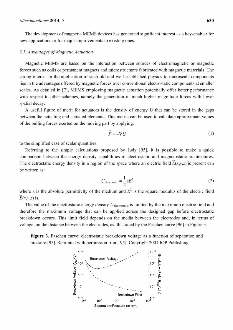
voltage, on the distance between the electrodes, as illustrated by the Paschen curve [96] in Figure 3.
Figure 3. Paschen curve: electrostatic breakdown voltage as a function of separation and
pressure [95]. Reprinted with permission from [95]. Copyright 2001 IOP Publishing.
Micromachines 2014, 5 631
It is known that devices with very small electrode spacing depart from the behaviour predicted by
Paschen’s law [97], and systematic studies of the electrical breakdown have been published for
applications of interest for MEMS [98]. A typical limit field value of 3 MV·m−1 yields an energy
density in vacuum of the order of 40 J·m−3 [7,95]. It is then possible to perform a similar calculation
for the case of magnetostatic actuators. In this case the energy density Umagnetostatic of a region of the
space where a magnetic flux density B(x,y,z) is present can be written as:
21
2 μmagnetostatic
BU = (3)
where µ is the permeability of the medium and B2 is the square modulus of the magnetic flux density
B(x,y,z). The value of the magnetostatic energy density Umagnetostatic is limited by the saturation flux
density, Bsat, of a magnetic material or by the maximum magnetic flux density generated by an
electromagnet. For a system with a mid-range flux density in the order of 0.1 T, the associated
magnetostatic energy density is around 4000 J·m−3, using the vacuum permeability value µ0 = 4π × 10−7 V·s·A−1·m−1. It is clear from the ratio of these two values ( 210/magnetostatic electrostaticU U ≈ )
that magnetostatic architectures have a higher energy capability per unit volume. This result is
obtained on quantities that represent energy densities, and are thus to a certain extent independent of
the dimensions of the fabricated structures. Figure 4 shows a comparison of the energy densities for
electrostatic actuators at different voltages and actuators based on magnetic materials such as iron or
nickel as a function of the gap distance [95]. The plot shows that there are indeed crossover points
where electrostatic systems have greater energy capacity, but this only occurs for very small distances
or very high voltages. Unfortunately, both these conditions do not fall into viable ranges for
application in integrated MEMS devices.
Figure 4. Comparison of electrostatic and magnetic energy densities as a function of
characteristic gap dimensions for various voltages [95]. The dotted line is derived from the
Paschen curve [96]. Reprinted with permission from [95]. Copyright 2001 IOP Publishing.
3.2. Excitation Sources
The previous simple arguments favor magnetostatic actuation over electrostatic actuation in terms
of the ability to exert intense forces. There are, however, a number of complications associated with
Micromachines 2014, 5 632
magnetic architectures. While electrostatic actuators only require conductive structures and the
application of a voltage, magnetic devices must include excitation field sources such as permanent
magnets or microcoils. Permanent magnets are great sources of fixed and stable bias fields that can be
locally amplified by small patterned structures of soft magnetic material [99]. To achieve a sufficiently
uniform bias magnetic flux density over the desired region, however, large permanent magnets are
normally required and must be fixed at a sufficiently small distance from the device region to ensure a
proper spatial field distribution, as illustrated in Figure 5.
Figure 5. Example of MEMS mounted on permanent magnet assembly, exploded
view [100]. Reprinted with permission from [100]. Copyright 2004 IEEE.
A number of devices have been reported that employ external permanent magnets to obtain bistable
or latching state configurations for magnetic MEMS devices [100,101]. This solution, however, makes
it impossible to integrate them into a standard IC process flow and requires additional assembly stages
to make the component operational.
Many researchers in the field of magnetic MEMS advocate the use of microformed permanent
magnets as integrated components embedded in the microelectromechanical structures as an alternative
to externally mounted permanent magnets, and the scaling of permanent magnets to dimensions of the
range of interest for microsystems has been documented [102]. A comprehensive work published in
2009 by Arnold reviewed the reported literature on microfabricated permanent magnets [103].
Sputtered [104–106], electroplated [91,107–110] and pulsed-laser [111–113] deposited micromagnets
have demonstrated excellent magnetic performance at thicknesses up to 100 µm, whereas
powder-based fabrication methods facilitate the manufacture of larger structures (up to 1 mm) but with
limited properties [114–116]. However, the best micromagnets are conventionally deposited rare earth
alloys, whose processing unfortunately presents insurmountable challenges that hinder their viability for
integration, such as the need for special substrates and high-temperature annealing treatments [103], and
exhibit an inconveniently high corrosion rate [117].
The third option involves the patterning of microcoils, a choice that implies an increased level of
complication in terms of both design and fabrication and is being actively pursued by many research
Micromachines 2014, 5 633
groups [118–121]. The magnetic field generation requires an electrical current flow, which has a
dramatic impact on the power dissipation and thermal budget characteristics of the manufactured
components. Self-heating of the windings poses a reliability issue as the metal tends to expand while
embedded in the insulating matrix, e.g., SU-8 [122–124] or Parylene [125–127]. This can potentially
force an uncontrolled stress load on the device. These downsides weigh even more when compared
with the freely available field source from the residual magnetisation of a permanent magnet. Even the
scaling laws identify permanent magnets as better components for miniaturisation than electromagnets,
as illustrated in Figure 6. The same considerations on current densities, heating and scalability led
Cugat et al. to the conclusion that micromagnets smaller than 100 µm are difficult to replace
with microcoils [128].
However, the fabrication processes required to manufacture microcoils are well established in the
industry and readily available within standard silicon cleanrooms, accompanied by significant
expertise built over the years on conventional IC and MEMS processing techniques.
Figure 6. Scaling of the current density in a microcoil for equivalence to a 1 T permanent
magnet of the same size [128]. Reprinted with permission from [128]. Copyright 2003 IEEE.
4. Examples of Magnetic MEMS Switches Reported in the Literature
Pioneering work on the integration of magnetic microactuators has been published by Ahn et al. [129],
demonstrating back in 1993 the functional device shown in Figure 7, which is fully compatible with
standard IC processing.
A few years later, in 1997, Judy et al. introduced the concepts of magnetic actuation by means of local
magnetic forces generated by microcoils and electrostatic latching mechanisms [130], for which a patent
was subsequently granted [131]. Conceptual schemes of potential microdevices are shown in Figure 8.
In the same year Wright et al. demonstrated a large force fully integrated electromagnetic
actuator [17] that comprises a cantilever beam and a planar electromagnetic coil fabricated through
surface and bulk micromachining.
The following sections review some of the most relevant MEMS switching devices reported in the
literature, in chronological order, with a particular focus on relays that employ magnetic actuation.
Micromachines 2014, 5 634
Figure 7. Concept and fabrication of a fully integrated magnetic microactuator [129].
(a) Concept of meander core and corresponding model; (b) Micrograph of the fabricated
microactuator; and (c) Scheme of the microactuator. Reprinted with permission from [129].
Copyright 1993 IEEE.
Figure 8. Scheme of potential microactuators employing (a) microfabricated coils for local
magnetic actuation and (b) electrostatic clamping for latching the actuated state [130].
Reprinted with permission from [130]. Copyright 1997 IEEE.
4.1. Taylor et al. (1998) [132]
The first of these devices was reported by Taylor et al. back in 1998 [132], as a follow-up on their
previous work [133]. The authors specifically address the incompatibility of previously reported
magnetic microrelays for IC integration and propose a device that is fully integrated and comprises a
single-layer coil that actuates an upper movable magnetic structure. The production of the device uses
low temperature fabrication processes (less than 250 °C) to guarantee compatibility with packaging
technologies and to ensure the possibility of manufacturing on substrates already processed with
silicon IC. A schematic of the device is presented in Figure 9.
Micromachines 2014, 5 635
Figure 9. Top view (a) and cross-section (b) of the device presented by Taylor et al. [132].
The magnetic movable plate is attracted to the substrate when a current is passed in the
meander coil to generate a magnetic pulling force. Reprinted with permission from [132].
Copyright 1998 IEEE.
The fabrication is based on a series of electroplating processes to produce the coils, the bottom and
side magnetic cores and the magnetic movable plate. Polyimide is used as a mould for electroplating
and as filling material to insulate the coils and the magnetic structures, whereas the movable plate is
formed by surface micromachining. The magnetic components are formed with electroplated Ni-Fe.
As shown in Figure 9, the relay is normally open and is actuated by flowing an adequate current in the
planar coil, which generates a magnetic flux that excites the magnetic structures. A magnetic flux
distribution is then formed, subsequently encountering a high reluctance gap between the top surfaces
of the core and the bottom surface of the upper plate. A force is exerted on the movable plate, which is
attracted to the electromagnet and connects the two ends of the conduction line. Upon removing the
excitation current, the elastic restoring forces in the suspension arms bring the structure back to its
relaxed position, returning the relay to the OFF state.
The device shows great performance in terms of actuation force, thus resulting in a low contact
resistance. The lowest force value of 0.1 mN was achieved at a coil current of 200 mA, allowing for a
maximum contact resistance of 38.6 mΩ. The device, however, requires a constant current feed to
maintain the ON state, resulting in high power consumption, which rules it out for many applications
(e.g., mobile). Additionally the presence of two contacts doubles the probability of failures as outlined
in Section 2.2.3.
4.2. Ruan et al. (2001) [78,134]
One of the first attempts to produce magnetically actuated microrelay with latching functionality was
reported in 2001 by Ruan et al [78,134]. A bistable configuration is achieved by the superimposition of
two magnetic effects. A hinged Ni–Fe cantilever is surface micromachined on top of a planar Ag
Micromachines 2014, 5 636
patterned coil, and the whole assembly is then mounted on top of a permanent magnet, as illustrated in
Figure 10.
Figure 10. Top view (top) and cross-section (bottom) of the device proposed by
Ruan et al. [78]. The device is mounted on a permanent magnet that provides the field needed
for the operation. Reprinted with permission from [78], page 347. Copyright 2001 Elsevier.
Microcantilevers are highly anisotropic structures that strongly favor magnetization along their easy
axis corresponding to their length [10]. A magnetized cantilever in an external bias field experiences a
torque that tends to align the magnetization M to the field axis and orientation. The devised
architecture utilizes the embedded Ag coil to force the cantilever in one of two possible magnetic
states, depending on the polarity of the applied voltage, thus magnetizing the cantilever along its length
in either direction. The bias field provided by the permanent magnet then exerts a torque on the hinged
cantilever, pulling either of its ends towards the bottom substrate while the other end is pushed
upwards. Figure 11 contains a scheme of the geometric configuration of the magnetic vectors. Once
the cantilever is forced in a magnetic state, and is consequently aligned to the bias field, the electrical
current can be turned off, as the magnetization is then induced solely by the bias field. Mechanical
stability can be achieved with the balance between the magnetic torque and the restoring resistance to
torsion of the hinges.
Figure 11. Scheme of the magnetic vectors in the device proposed by Ruan et al. [134],
where m is the cantilever magnetisation and H0 is the bias magnetic field. Reprinted with
permission from [134]. Copyright 2001 IEEE.
Micromachines 2014, 5 637
The bistable latching device offers great performance in terms of power consumption, as only short
current pulses are needed to excite the magnetic cantilever. Low contact resistance values are also
measured, in the range of 50 to 70 mΩ. On the down side, the device requires assembling onto a
permanent magnet, hindering the possible integration in a standard IC process flow, and presents a
two-contact architecture, more prone to failures.
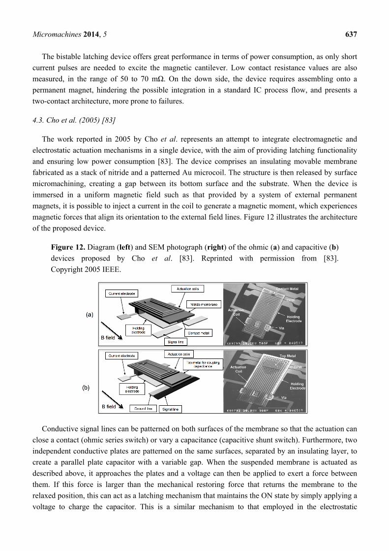
4.3. Cho et al. (2005) [83]
The work reported in 2005 by Cho et al. represents an attempt to integrate electromagnetic and
electrostatic actuation mechanisms in a single device, with the aim of providing latching functionality
and ensuring low power consumption [83]. The device comprises an insulating movable membrane
fabricated as a stack of nitride and a patterned Au microcoil. The structure is then released by surface
micromachining, creating a gap between its bottom surface and the substrate. When the device is
immersed in a uniform magnetic field such as that provided by a system of external permanent
magnets, it is possible to inject a current in the coil to generate a magnetic moment, which experiences
magnetic forces that align its orientation to the external field lines. Figure 12 illustrates the architecture
of the proposed device.
Figure 12. Diagram (left) and SEM photograph (right) of the ohmic (a) and capacitive (b)
devices proposed by Cho et al. [83]. Reprinted with permission from [83].
Copyright 2005 IEEE.
Conductive signal lines can be patterned on both surfaces of the membrane so that the actuation can
close a contact (ohmic series switch) or vary a capacitance (capacitive shunt switch). Furthermore, two
independent conductive plates are patterned on the same surfaces, separated by an insulating layer, to
create a parallel plate capacitor with a variable gap. When the suspended membrane is actuated as
described above, it approaches the plates and a voltage can then be applied to exert a force between
them. If this force is larger than the mechanical restoring force that returns the membrane to the
relaxed position, this can act as a latching mechanism that maintains the ON state by simply applying a
voltage to charge the capacitor. This is a similar mechanism to that employed in the electrostatic
Micromachines 2014, 5 638
microrelays described in Section 2, with the further advantage of latching the switch in position once the
gap is sufficiently reduced by the big initial approach driven by the long-range electromagnetic forces.
The large forces generated by electromagnetic actuation allow for stiffer structures and the use of
external permanent magnets as the uniform bias field source allows actuation over very large gaps, as
the amplitude of the exerted force in this case does not depend on the distance. This guarantees, in
turn, excellent performances in terms of isolation in the OFF state. The experimental data reported in
Figure 13 shows that, with minimal actuation current of less than 60 mA, the membrane can be easily
displaced for actuation over gaps of big dimensions, following a linear trend.
The electrostatic hold voltage is also very low (<3.7 V) as it intervenes when the gap between the
latching capacitor plates is already minimized by the electromagnetic interaction. The energy
consumption is calculated to be less than 87.9 µJ per switching cycle. A further advantage of this
design is that the transition to the OFF state is aided by passing a current through the actuation coil of
the opposite polarity with respect to the ON-state actuation current. The generated magnetic repulsion
from the external permanent magnet adds to the mechanical restoring force of the membrane, and
helps prevent stiction.
Figure 13. Displacement as function of actuation current in the device proposed by
Cho et al. [83]. Reprinted with permission from [83]. Copyright 2005 IEEE.
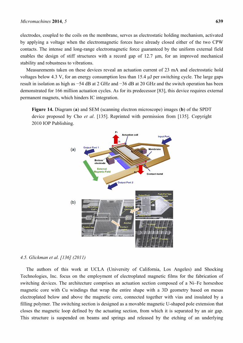
4.4. Cho et al. (2010) [135]
A second latching microrelay was reported by Cho et al. [135] in the form of a single-pole
double-throw (SPDT) switch with combined electromagnetic and electrostatic actuation to achieve
operation at low power and low voltage. The proposed device is based on the same operation principle
previously published by the same group and described in Section 4.3, relying on an external bias field
for the creation of stable magnetic states. The same architecture is hence once again used with a
different application but no substantial technological modifications. Figure 14 details a diagram and
SEM (scanning electron microscope) images of the SPDT device.
A dielectric membrane with integrated coils is hinged and suspended by two dielectric torsion bars
that allow its rotation. The electromagnetic forces generated on the coils by a uniform external
magnetic field provided by permanent magnets exerts a torque on the membrane system, which rotates
and closes one of the two lateral Co-Planar Waveguide (CPW) lines. A pair of patterned bottom
Micromachines 2014, 5 639
electrodes, coupled to the coils on the membrane, serves as electrostatic holding mechanism, activated
by applying a voltage when the electromagnetic forces have already closed either of the two CPW
contacts. The intense and long-range electromagnetic force guaranteed by the uniform external field
enables the design of stiff structures with a record gap of 12.7 μm, for an improved mechanical
stability and robustness to vibrations.
Measurements taken on these devices reveal an actuation current of 23 mA and electrostatic hold
voltages below 4.3 V, for an energy consumption less than 15.4 μJ per switching cycle. The large gaps
result in isolation as high as −54 dB at 2 GHz and −36 dB at 20 GHz and the switch operation has been
demonstrated for 166 million actuation cycles. As for its predecessor [83], this device requires external
permanent magnets, which hinders IC integration.
Figure 14. Diagram (a) and SEM (scanning electron microscope) images (b) of the SPDT
device proposed by Cho et al. [135]. Reprinted with permission from [135]. Copyright
2010 IOP Publishing.
4.5. Glickman et al. [136] (2011)
The authors of this work at UCLA (University of California, Los Angeles) and Shocking
Technologies, Inc. focus on the employment of electroplated magnetic films for the fabrication of
switching devices. The architecture comprises an actuation section composed of a Ni–Fe horseshoe
magnetic core with Cu windings that wrap the entire shape with a 3D geometry based on mesas
electroplated below and above the magnetic core, connected together with vias and insulated by a
filling polymer. The switching section is designed as a movable magnetic U-shaped pole extension that
closes the magnetic loop defined by the actuating section, from which it is separated by an air gap.
This structure is suspended on beams and springs and released by the etching of an underlying
Micromachines 2014, 5 640
sacrificial layer to allow horizontal movement. The four-arm architecture with the serpentine design
ensures appropriate stiffness and in-plane movement. Figure 15 illustrates the concept drawing and the
fabricated device.
The switch contact is designed as a vertical surface contact, as shown in greater detail in Figure 16,
that closes with the horizontal movement of the U-shaped pole extension.
Figure 15. Drawing (left) and SEM micrograph (right) of the horseshoe-shaped magnetic
switch proposed by Glickman et al. [136]. Reprinted with permission from [136].
Copyright 2011 IEEE.
Figure 16. Glickman et al. SEM detail of the switch contact [136]. Reprinted with
permission from [136]. Copyright 2011 IEEE.
By passing an electrical current into the coil, the Ni–Fe core is excited with a magnetization vector
M that follows the shape of the structure. The magnetic field distribution generated by the magnetized
structure in the surrounding space excites in turn the pole extension, which is then attracted to the field
source in an attempt to minimize the high reluctance space region of the gap.
A complete actuation model based on reluctance paths is proposed and a comprehensive set of
measurements is presented. The prototype does not include any latching mechanism to improve the
power consumption characteristics, and the horizontal actuation geometry offers little opportunity for
the implementation of conventional mechanisms, unless micromechanical latching is considered with
physical hooks and anchors [9,137], which introduce a further manufacturing complication and
requires a larger area.
Micromachines 2014, 5 641
5. Discussion
5.1. Summary of the Reviewed Devices: Classification by Smart Power Handling and Full Integrability
The main challenge posed by the manufacturing of magnetic MEMS is the development of efficient
and reliable processing techniques to integrate soft magnetic materials within conventionally fabricated
electrical and mechanical structures. Table 3 is a summary of some of the features of the magnetic
MEMS relays that have been discussed, along with other reported devices. Many publications report
RF measurements, namely insertion loss and isolation, on the proposed devices, and these results are
not included but can be consulted in the articles referenced in the first column.
It is clear that most of the magnetic MEMS switches reported in the literature employ external
permanent magnets to bias the space surrounding the contacts and exert force on the desired
components or maintain the actuated state. This is obviously a disadvantage if the switches are to be
integrated with Metal-Oxide-Semiconductor (MOS) technology and compatibility with standard IC
processing is required. On the other hand, the devices reported in the literature that are IC compatible
do not integrate latching mechanisms that enable efficient power management.
Table 3. Magnetic MEMS switches reported in the literature, in chronological order.
Group Actuation
mechanism
Contact
Resistance
(mΩ)
Power Consumption Switch
Speed (ms)
Compatible
with Full IC
Integration 1
Latch
Function 2
Taylor et al. (1998) [132] Magnetic 24–38 33–320 mW 0.5–5
Ruan et al. (2001) [78,134] Magnetic 50–70 <93 µJ/switch cycle ~0.2
Magfusion, Inc (2004) [138] Magnetic 500 2.5 mJ/switch cycle 0.2