Integrated One Diode−One Resistor Architecture in Nanopillar SiOxResistive Switching Memory by Nanosphere LithographyLi Ji,† Yao-Feng Chang,*,† Burt Fowler,‡ Ying-Chen Chen,⊥ Tsung-Ming Tsai,§ Kuan-Chang Chang,§
Min-Chen Chen,∥ Ting-Chang Chang,∥ Simon M. Sze,⊥ Edward T. Yu,† and Jack C. Lee†
†Microelectronics Research Center, The University of Texas at Austin, Austin, Texas 78758, United States‡PrivaTran, LLC, 1250 Capital of Texas Highway South, Building 3, Suite 400, Austin, Texas 78746, United States§Department of Materials and Optoelectronic Science and ∥Department of Physics, National Sun Yat-Sen University, Kaohsiung,Taiwan⊥Department of electronics engineering and Institute of Electronics, National Chiao Tung University, Hsinchu 300, Taiwan
*S Supporting Information
ABSTRACT: We report on a highly compact, one diode−oneresistor (1D−1R) nanopillar device architecture for SiOx-basedReRAM fabricated using nanosphere lithography (NSL). Theintrinsic SiOx-based resistive switching element and Si diode areself-aligned on an epitaxial silicon wafer using NSL and a deep-Si-etch process without conventional photolithography. AC-pulse response in 50 ns regime, multibit operation, and goodreliability are demonstrated. The NSL process provides a fastand economical approach to large-scale patterning of high-density 1D−1R ReRAM with good potential for use in futureapplications.
In recent years, resistive random access memory (ReRAM)has drawn much interest as a promising candidate for next
generation nonvolatile memory due to its potential scalabilitybeyond 10 nm feature size using a crossbar structure, fastswitching speed, low operating power, and good reliability.1−3
Traditional charge-based nonvolatile memory (NVM) typicallyincludes a charge “trapping layer” within a transistorconfiguration that requires a high thermal budget and largefootprint (typically 6F2, where F = minimum feature size).4,5
Resistive switching (RS) memory operates by controllingdevice resistance with an external electrical manipulation,6−9
leading to better electrical performance, smaller design area(4F2), and excellent cycling endurance.10 Resistive-basedmemories are a new class of devices compatible withapplications that go beyond traditional electronics configu-rations, for example, three-dimension (3D) stacking, nano-battery, neuro-electronics and Boolean logic opera-tions.11,12,13,14−17
There have been many studies of binary-metal oxideresistance switching characteristics,17,18 which can haveoperating instability issues due to difficulty in controllingstoichiometric compositions.19,20 Therefore, a simple processthat is compatible with conventional CMOS fabrication allowsmultilayer compositional engineering and provides goodelectrical stability and high yield are critical requirements forReRAM commercialization.21 Silicon oxide (SiOx) has longbeen used as gate dielectrics for metal−oxide−semiconductor
field-effect transistors. In addition to its excellent insulatingproperties, SiOx-based resistive switching phenomena havebeen observed as early as 1962 by Hickmott and 1967 bySimmons and Verderber and have further been modeled byDearnaley in the 1970s.22−24 They observed that a simple M−I−M structure (ex. Au/SiOx/Al) can form an active devicebased on its repeatable negative resistance phenomenon.Recently, Yao et al. have reported SiOx-based resistiveswitching behaviors in vacuum (1R), indicating that thistraditionally passive material can be converted to an activememory element and controlled by external electricalactivation.25−27 Furthermore, G. Wang et al. report anintegrated Schottky diode-1R configuration that demonstrateshigh performance and low power in a 1k-bit array for potentialcircuit-level applications.28 However, considering the staticpower consumption and sneak-path issues in large-scale,crossbar array designs,29−31 a Schottky-diode is not suitablefor portable electronics due to its high reverse-bias leakagecurrent and relatively low reverse-bias breakdown voltage ascompared to a Si-based PN-diode or transistor.32−34 Forexample, the reverse leakage current of Schottky diodes canincrease dramatically with temperature to the point of a
Received: November 8, 2013Revised: December 16, 2013Published: December 26, 2013
thermal-runaway situation,35 potentially resulting in instabilityissues and readout failures.In this work, a Si diode (1D) with low reverse-bias current is
integrated with a SiOx-based memory element (1R) usingnanosphere lithography (NS lithography, or NSL) and deep-Si-etching (DES) to pattern a P2+/N+/N2+ epitaxial Si wafer. Theself-aligned process forms a high density, large-scale nanopillar(NP) array architecture. Compared with conventional photo-lithography or direct-writing methods (such as electron beamlithography or focused ion beam milling), NSL has emerged asa low-cost (maskless), high-throughput alternative technique topattern large areas.36−39 The nanostructures fabricated usingNSL can be well-controlled in shape, size, and interpillarspacing through direct assembly of polymer nanospheres on thewafer-scale. Performance of 1R and 1D−1R structures arecharacterized and show that the integrated nanopillar 1D−1Rconfiguration offers low static-power for suppression of sneak-path issues. The work reported here provides an efficientfabrication process and low reverse-bias current in a SiOx-based1D−1R configuration for potential use in future ultralarge-scaleNVM applications.Experiment. Figure 1 illustrates the process flow for a 1R
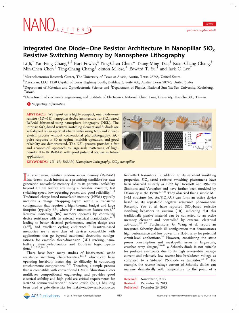
SiOx-based ReRAM with sequential scanning electron micro-scope images (Zeiss Neon 40 SEM) of the evolving structures.The detailed procedure of 1R SiOx-based ReRAM arrayfabrication begins with e-beam evaporation (PVD, CHAIndustries) of 60 nm of SiOx (measured by ellipsometer) ona N2+ (100) Si substrate (1−7 × 1019 cm−3, resistivity of0.001−0.005 ohm-cm) used as a bottom electrode. The SiOxacts as the 1R element and as a hardmask for self-aligned 1Dnanopillar fabrication (as describe further below). Next, thePVD-SiOx layer is treated in an oxygen plasma reactor to obtain
a hydrophilic surface. 18 MΩ DI water and 200 nm polystyrenenanospheres (Polysciences, Inc.) were used for nanospheremask preparation. The 200 nm nanosphere was chosen due to atrade-off between minimum feature size and larger-scaleuniformity as described in Supporting Information Figure S1.Polystyrene nanosphere solution was dropped on top ofmicroscope coverslips. This was then introduced to air−waterinterface in a Petri dish filled with 18MΩ DI water. Thepolystyrene solution spreads out at the air−water interfaceforming a monolayer. Prior to monolayer formation, a preparedsilicon substrate with SiOx coating was immersed at the bottomof a Petri dish. The monolayer was then transferred to animmersed substrate by slightly lifting the substrate. Then thesample was dried in air. The diameter of each NS in themonolayer was reduced by reactive ion etching (Oxford 80RIE) in oxygen-plasma (80 sccm O2; power 60 W; pressure 100mT; 1 min). The power, partial pressure, and time of etchingwere optimized to obtain the desired size (Figure 1b andSupporting Information Figure S2). The 1R array is formed byRIE (5 sccm Ar + 5 sccm O2 + 80 sccm CF4; power 100 W;pressure: 200 mT) to transfer the treated NS pattern into theSiOx layer (Figure 1c with average diameter of about 150 nm,see Supporting Information Figure S2). The NS layer wasremoved by bath sonication in water for 15 min. For the 1D−1R structure, a P2+/N+/N2+ epitaxial Si wafer is used as thesubstrate (P2+, thickness 0.3 um, boron (B), concentration 5 ×1019 cm−3; N+, thickness 0.6 um, arsenic (As), concentration 5× 1016 cm−3; N2+, substrate, phosphorus (P), concentration 1−7 × 1019 cm−3). On the basis of the 1R array, nanopillars areobtained via Bosch deep silicon etch process (Versaline DeepSilicon Etch System, Plasma-Therm Inc.) as shown inSupporting Information Figure S3. A tungsten (W) probe tip
Figure 1. The 1R process flow using nanosphere (NS) lithography: (a) NS deposition on 60 nm thick SiOx and N2+ Si substrate as a bottomelectrode. (b) RIE oxygen plasma shrinks the diameter of polystyrene NSs. (c) The 1R array is formed by SiOx RIE to transfer the NS pattern intothe SiOx layer to complete 1R formation.
Nano Letters Letter
dx.doi.org/10.1021/nl404160u | Nano Lett. 2014, 14, 813−818814
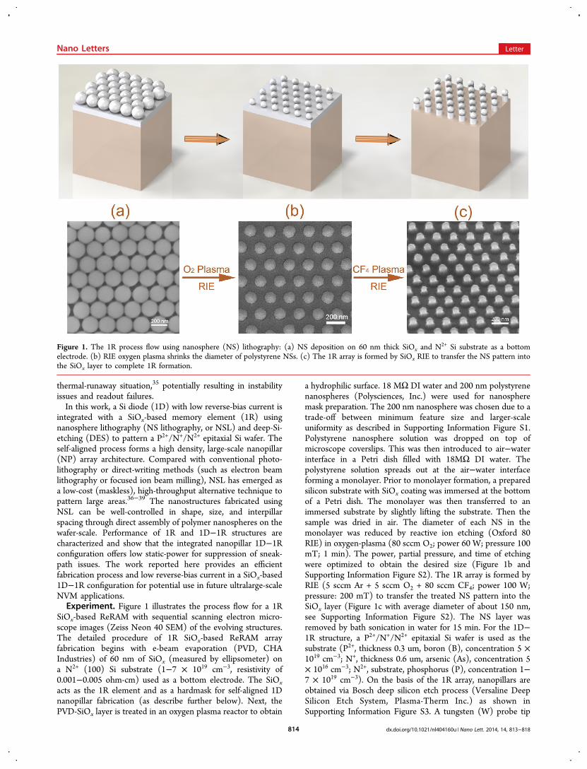
(∼10 um radius) was used as a top electrode, and a Lake ShoreCryotronics vacuum probe chamber (<1 mTorr) and AgilentB1500A device analyzer were used for electrical test. I−V datawere collected using AC pulse and forward/reverse DC sweeps:the Set process programs the device to a conductive, low-resistive state (LRS); the Reset process programs each device toa low-conductance, high-resistive state (HRS) having lowerconductance as reset stop voltage is increased.Results and Discussions. Figure 2 shows I−V character-
istics of direct current (dc) sweep and alternating current (ac)pulse response for SiOx-based 1R array fabricated by NSL.Voltage was applied to the top electrode (W probe tip) withbottom electrode (N2+ Si substrate) at ground. All testing wasdone in vacuum. To establish reversible switching in thesedevices, a two-step electroforming process was used: (1) acurrent-limited voltage sweep to induce soft breakdown; and(2) a forward/backward voltage sweep to electroform thedevice. The soft-breakdown process is done by sweeping thevoltage until current dramatically increases to a compliancecurrent limit (CCL), typically 100 nA in this work. Generally,this process avoids hard breakdown and increases electro-forming yield in most types of ReRAM devices.8,17 For theSiOx-based ReRAM devices used here, a second electroformingstep was done using a forward/backward voltage sweep (Figure2a), where current fluctuations are observed to increase toabove the CCL during the forward voltage sweep. Electro-forming is completed during the backward voltage sweep fromthe forming voltage (about 8−18 V within 12 devices, inset of
Figure 1b) to 0 V, resulting in a LRS. After the electro-formation, resistive switching performance is stabilized bycycling the device multiple times using voltage sweeps (Figure2b). The Set process is a 4 V forward/reverse sweep withoutany CCL to program the device to the LRS. The Reset processis done by sweeping the voltage to 8 V, where the currentdecreases as the voltage is swept from about 5 to 8 V and thedevice is programmed into an HRS. The HRS/LRS resistanceratio is at least ∼50 at 1 V bias, which satisfies sensingrequirements.3,32 Figure 2c demonstrates the ac pulse responsefor Set and Reset programming in the 50 ns regime where HRSand LRS resistance values are controlled by applied pulse heightand pulse width, thus potentially enabling multilevel program-ming in a single memory cell. Figure 2d shows HRS and LRSresistance values during 104 switching cycles. A resistance ratioof at least 1 order of magnitude is maintained, although soft-errors were observed during the first 100 cycles (inset of Figure2d). It may be noted that the electroforming voltages measuredhere (∼12 V) are somewhat lower than those measured inprevious work on MOSCAP device architectures40,41 and arenear the voltage used in the Reset process (8 V). This could bedue to creation of electrically active defects near the SiOxsidewall during the RIE process that may lower the softbreakdown threshold and reduce the filament formation energyduring the subsequent electroforming process. Also, the resetvoltage (i.e., the voltage at which LRS current begins todecrease) is always greater than or equal to the set voltage(where current increases sharply), which is a unique character-
Figure 2. DC sweep resistive switching behaviors and ac pulsed response of 1R element: (a) Electrical soft-breakdown process with 100 nAcompliance current limit, and forward/backward voltage sweep electroforming process. (b) Ten I−V resistive switching set/reset cycles. The insetshows the measured electroforming voltage distribution. (c) The ac pulsed switching properties with fixed reset pulse width (dc Set) and fixed setpulse height conditions (dc Reset). (d) HRS and LRS endurance data during ac voltage cycling. At least a one-order-of-magnitude resistance ratio ismaintained after 104 cycles.
Nano Letters Letter
dx.doi.org/10.1021/nl404160u | Nano Lett. 2014, 14, 813−818815
istic of SiOx-based ReRAM as compared to other materialsystems.18 The difference between reset and set voltages canpotentially be controlled by optimizing the series resistance inthe circuit and choice of electrode materials.41
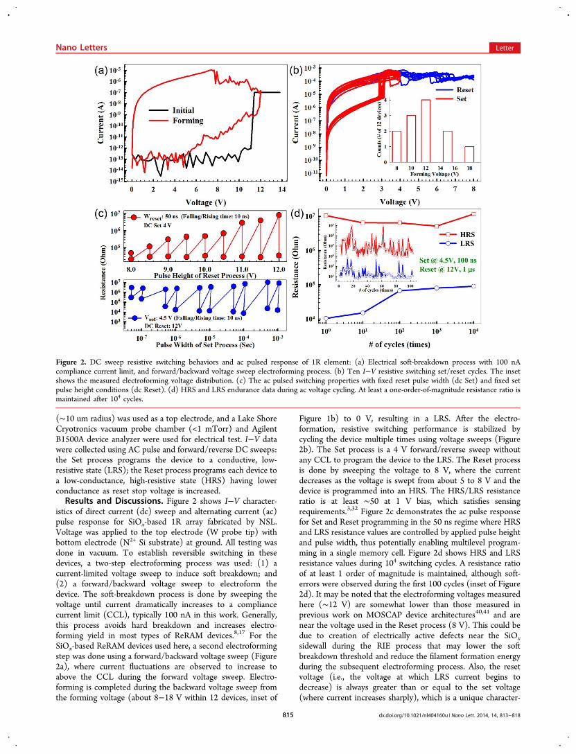
Figure 3 illustrates the 1D−1R NP fabrication process andshows SEM images of a NP array. Nanopillars are formed andseparated by the DSE process in Bosch mode, which containsthree steps: (1) polymer deposition; (2) polymer etching; and(3) Si etching (Supporting Information Figure S3 shows theprocedure in detail). The etch time and power in the Boschprocess were optimized to reduce sidewall scalloping (Figure3b and Supporting Information Figure S4). Figure 3c shows a 2in. wafer used to demonstrate the 1D−1R fabrication processusing an epitaxial 1D structure. Additional work is in progressto optimize the across-wafer uniformity of the NSL and DSE
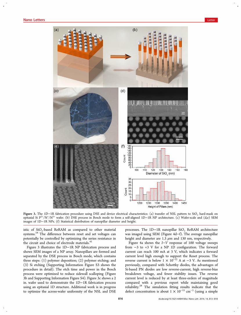
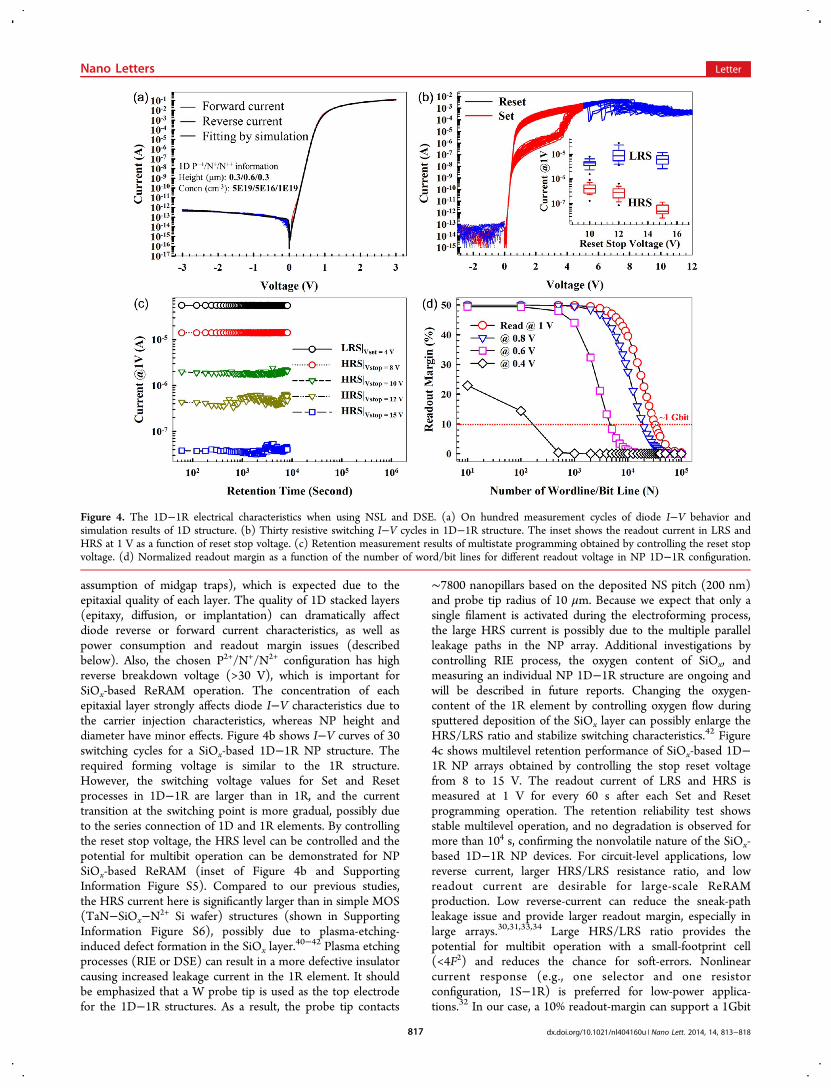
processes. The 1D−1R nanopillar SiOx ReRAM architecturewas imaged using SEM (Figure 4d−f). The average nanopillarheight and diameter are 1.3 μm and 130 nm, respectively.Figure 4a shows the I−V response of 100 voltage sweeps
from −3 to +3 V for a NP 1D configuration. The forwardcurrent can reach 100 mA at 3 V, which indicates a forwardcurrent level high enough to support the Reset process. Thereverse current is below 1 × 10⁻¹² A at −3 V. As mentionedpreviously, compared with Schottky diodes, the advantages ofSi-based PN diodes are low reverse-current, high reverse-biasbreakdown voltage, and fewer stability issues. The reversecurrent level is reduced by at least three-orders of magnitudecompared with a previous report while maintaining goodreliability.28 The simulation fitting results indicate that thedefect concentration is about 1 × 10⁻¹⁵ cm−3 (using a simple
Figure 3. The 1D−1R fabrication procedure using DSE and device electrical characteristics: (a) transfer of NSL pattern to SiOx hard-mask onepitaxial Si P2+/N+/N2+ wafer. (b) DSE process in Bosch mode to form a self-aligned 1D−1R NP architecture. (c) Wafer-scale and (d,e) SEMimages of 1D−1R NPs. (f) Statistical distribution of nanopillar diameter and height.
Nano Letters Letter
dx.doi.org/10.1021/nl404160u | Nano Lett. 2014, 14, 813−818816
assumption of midgap traps), which is expected due to theepitaxial quality of each layer. The quality of 1D stacked layers(epitaxy, diffusion, or implantation) can dramatically affectdiode reverse or forward current characteristics, as well aspower consumption and readout margin issues (describedbelow). Also, the chosen P2+/N+/N2+ configuration has highreverse breakdown voltage (>30 V), which is important forSiOx-based ReRAM operation. The concentration of eachepitaxial layer strongly affects diode I−V characteristics due tothe carrier injection characteristics, whereas NP height anddiameter have minor effects. Figure 4b shows I−V curves of 30switching cycles for a SiOx-based 1D−1R NP structure. Therequired forming voltage is similar to the 1R structure.However, the switching voltage values for Set and Resetprocesses in 1D−1R are larger than in 1R, and the currenttransition at the switching point is more gradual, possibly dueto the series connection of 1D and 1R elements. By controllingthe reset stop voltage, the HRS level can be controlled and thepotential for multibit operation can be demonstrated for NPSiOx-based ReRAM (inset of Figure 4b and SupportingInformation Figure S5). Compared to our previous studies,the HRS current here is significantly larger than in simple MOS(TaN−SiOx−N2+ Si wafer) structures (shown in SupportingInformation Figure S6), possibly due to plasma-etching-induced defect formation in the SiOx layer.
40−42 Plasma etchingprocesses (RIE or DSE) can result in a more defective insulatorcausing increased leakage current in the 1R element. It shouldbe emphasized that a W probe tip is used as the top electrodefor the 1D−1R structures. As a result, the probe tip contacts
∼7800 nanopillars based on the deposited NS pitch (200 nm)and probe tip radius of 10 μm. Because we expect that only asingle filament is activated during the electroforming process,the large HRS current is possibly due to the multiple parallelleakage paths in the NP array. Additional investigations bycontrolling RIE process, the oxygen content of SiOx, andmeasuring an individual NP 1D−1R structure are ongoing andwill be described in future reports. Changing the oxygen-content of the 1R element by controlling oxygen flow duringsputtered deposition of the SiOx layer can possibly enlarge theHRS/LRS ratio and stabilize switching characteristics.42 Figure4c shows multilevel retention performance of SiOx-based 1D−1R NP arrays obtained by controlling the stop reset voltagefrom 8 to 15 V. The readout current of LRS and HRS ismeasured at 1 V for every 60 s after each Set and Resetprogramming operation. The retention reliability test showsstable multilevel operation, and no degradation is observed formore than 104 s, confirming the nonvolatile nature of the SiOx-based 1D−1R NP devices. For circuit-level applications, lowreverse current, larger HRS/LRS resistance ratio, and lowreadout current are desirable for large-scale ReRAMproduction. Low reverse-current can reduce the sneak-pathleakage issue and provide larger readout margin, especially inlarge arrays.30,31,33,34 Large HRS/LRS ratio provides thepotential for multibit operation with a small-footprint cell(<4F2) and reduces the chance for soft-errors. Nonlinearcurrent response (e.g., one selector and one resistorconfiguration, 1S−1R) is preferred for low-power applica-tions.32 In our case, a 10% readout-margin can support a 1Gbit
Figure 4. The 1D−1R electrical characteristics when using NSL and DSE. (a) On hundred measurement cycles of diode I−V behavior andsimulation results of 1D structure. (b) Thirty resistive switching I−V cycles in 1D−1R structure. The inset shows the readout current in LRS andHRS at 1 V as a function of reset stop voltage. (c) Retention measurement results of multistate programming obtained by controlling the reset stopvoltage. (d) Normalized readout margin as a function of the number of word/bit lines for different readout voltage in NP 1D−1R configuration.
Nano Letters Letter
dx.doi.org/10.1021/nl404160u | Nano Lett. 2014, 14, 813−818817
array due to the low reverse-biased diode current and largeLRS/reverse-current ratio (Figure 4d). The results demon-strated here provide significant benefits by simplifying theReRAM fabrication process and potentially enabling compat-ibility with high-volume CMOS manufacturing.Summary. In summary, we have demonstrated high-
density, wafer-scale 1D−1R nanopillar SiOx-based ReRAMfabricated by nanosphere lithography. Excellent resistiveswitching characteristics and reliability are observed, the ACpulsed switching speed is in the 50 ns regime and multibitoperation is demonstrated. The Si-based epitaxial 1D NPstructure was formed by using a deep-Si-etch process. Lowreverse-bias diode current and nonlinear I−V characteristicshelp reduce sneak-path issues and further improve the readoutmargin in practical large-scale array designs up to 1 Gbit in size.The demonstrated technology has great potential not only formaskless electronics but also provides a fast and economicalsolution for wafer-scale manufacturing of high-density 1D−1RReRAM arrays.
■ ASSOCIATED CONTENT*S Supporting InformationMaterials and methods, Bosch process flow, and electricalproperties. This material is available free of charge via theInternet at http://pubs.acs.org.
■ ACKNOWLEDGMENTSThis material is based upon work partially supported by theJudson S. Swearingen Regents Chair in Engineering at TheUniversity of Texas at Austin (E.T.Y. and L.J) and Cullen Trustfor Higher Education Endowed Professorship in Engineering(J.L.)
■ REFERENCES(1) Lundstrom, M. Science 2003, 299, 210−211.(2) Leong, M.; Doris, B.; Kedzierski, J.; Rim, K.; Yang, M. Science2004, 306, 2057−2060.(3) Chen, Y. Y.; Degraeve, R.; Clima, S.; Govoreanu, B.; Goux, L.;Fantini, A.; Kar, G. S.; Pourtois, G.; Groeseneken, G.; Wouters, D. J.;Jurczak, M. IEEE Int. Electron Devices Meet., Tech. Dig. 2012, 482−485.(4) Kahng, D.; Sze, S. M. Bell Syst. Tech. J. 1967, 46, 1288−1295.(5) Chang, T. C.; Jian, F. Y.; Chen, S. C.; Tsai, Y. T. Mater. Today2011, 14, 608−615.(6) Lu, W.; Lieber, C. M. Nat. Mater. 2007, 6, 841−850.(7) Heath, J. R.; Ratner, M. A. Phys. Today 2003, 56, 43−49.(8) Sawa, A. Mater. Today 2008, 11, 28−36.(9) Terabe, K.; Hasegawa, T.; Nakayama, T.; Aono, M. Nature 2005,433, 47−50.(10) Lee, M.-J.; Lee, C. B.; Lee, D.; Lee, S. R.; Chang, M.; Hur, J. H.;Kim, Y.-B.; Kim, C.-J.; Seo, D. H.; Seo, S.; Chung, U. I.; Yoo, I.-K.;Kim, K. Nat. Mater. 2011, 10, 625−630.(11) Yu, S.; Chen, H. Y.; Gao, B.; Kang, J.; Wong, H.-S. P. ACS Nano2013, 7, 2320−2325.(12) Song, S.; Cho, B.; Kim, T. W.; Ji, Y.; Jo, M.; Wang, G.; Choe,M.; Kahng, Y. H.; Hwang, H.; Lee, T. Adv. Mater. 2010, 22, 5048−5052.(13) Valov, I.; Linn, E.; Tappertzhofen, S.; Schmelzer, S.; Hurk, J. V.D.; Lentz, F.; Waser, R. Nat. Commun. 2013, 4, 1771−1779.
(14) Jo, S. H.; Chang, T.; Ebong, I.; Bhadviya, B. B.; Mazumder, P.;Lu, W. Nano Lett. 2010, 10, 1297−1301.(15) Ohno, T.; Hasegawa, T.; Tsuruoka, T.; Terabe, K.; Gimzewski,J. K.; Aono, M. Nat. Mater. 2011, 10, 591−595.(16) Borghetti, J.; Snider, G. S.; Kuekes, P. J.; Yang, J. J.; Stewart, D.R.; Williams, R. S. Nature 2010, 464, 873−876.(17) Waser, R.; Aono, M. Nat. Mater. 2007, 6, 833−840.(18) Waser, R.; Dittmann, R.; Staikov, G.; Szot, K. Adv. Mater. 2009,21, 2632−2663.(19) Yang, J. J.; Pickett, M. D.; Li, X.; Ohlberg, D. A. A.; Stewart, D.R.; Williams, R. S. Nat. Nanotechnol. 2008, 3, 429−433.(20) Szot, K.; Speier, W.; Bihlmayer, G.; Waser, R. Nat. Mater. 2006,5, 312−320.(21) Meijer, G. I. Science 2008, 319, 1625−1626.(22) Hickmott, T. W. J. Appl. Phys. 1962, 33, 2669−2682.(23) Simmons, J. G.; Verderber, R. R. Proc. R. Soc. London, Ser. A1967, 301, 77−102.(24) Dearnaley, G.; Stoneham, A. M.; Morgan, D. V. Rep. Prog. Phys.1970, 33, 1129−1191.(25) Yao, J.; Sun, Z.; Zhong, L.; Natelson, D.; Tour, J. M. Nano Lett.2010, 10, 4105−4110.(26) Yao, J.; Lin, J.; Dai, Y.; Ruan, G.; Yan, Z.; Li, L.; Zhong, L.;Natelson, D.; Tour, J. M. Nat. Commun. 2012, 3, 1101.(27) Yao, J.; Zhong, L.; Zhang, Z.; He, T.; Jin, Z.; Wheeler, P. J.;Natelson, D.; Tour, J. M. Small 2009, 5, 2910−2915.(28) Wang, G.; Lauchner, A. C.; Lin, J.; Natelson, D.; Palem, K. V.;Tour, J. M. Adv. Mater. 2013, 25, 4789−4793.(29) Lee, M.-J.; Park, Y.; Suh, D.-S.; Lee, E.-H.; Seo, S.; Kim, D.-C.;Jung, R.; Kang, B.-S.; Ahn, S.-E.; Lee, C. B.; Seo, D. H.; Cha, Y.-K.;Yoo, I.-K.; Kim, J.-S.; Park, B. H. Adv. Mater. 2007, 19, 3919−3923.(30) Chang, S. H.; Lee, S. B.; Jeon, D. Y.; Park, S. J.; Kim, G. T.;Yang, S. M.; Chae, S. C.; Yoo, H. K.; Kang, B. S.; Lee, M. J.; Noh, T.W. Adv. Mater. 2011, 23, 4063−4067.(31) Linn, E.; Rosezin, R.; Kugeler, C.; Waser, R. Nat. Mater. 2010, 9,403−406.(32) Huang, J. J.; Tseng, Y. M.; Luo, W. C.; Hsu, C. W.; Hou, T. H.IEEE Int. Electron Devices Meet., Tech. Dig. 2011, 733−736.(33) Cho, B.; Kim, T.-W.; Song, S.; Ji, Y.; Jo, M.; Hwang, H.; Jung,G.-Y.; Lee, T. Adv. Mater. 2010, 22, 1228−1232.(34) Lee, M.-J.; Kim, S. I.; Lee, C. B.; Yin, H.; Ahn, S.-E.; Kang, B. S.;Kim, K. H.; Park, J. C.; Kim, C. J.; Song, I.; Kim, S. W.; Stefanovich,G.; Lee, J. H.; Chung, S. J.; Kim, Y. H.; Park, Y. Adv. Funct. Mater.2009, 19, 1587−1593.(35) Sze, S. M. Physics of Semiconductor Devices, 2nd ed.; Wiley: NewYork, 1981.(36) Hall, A. S.; Friesen, S. A.; Mallouk, T. E. Nano Lett. 2013, 13,2623−2627.(37) Madaria, A. R.; Yao, M.; Chi, C.; Huang, N.; Lin, C.; Li, R.;Povinelli, M. L.; Dapkus, P. D.; Zhou, C. Nano Lett. 2012, 12, 2839−2845.(38) Li, L.; Zhai, T.; Zeng, H.; Fang, X.; Bando, Y.; Golberg, D. J.Mater. Chem. 2011, 21, 40−56.(39) Hsu, C. M.; Connor, S. T.; Tang, M. X.; Cui, Y. Appl. Phys. Lett.2008, 93, 133109.(40) Chang, Y. F.; Ji, L.; Wu, Z. J.; Zhou, F.; Wang, Y.; Xue, F.;Fowler, B.; Yu, E. T.; Ho, P. S.; Lee, J. C. Appl. Phys. Lett. 2013, 103,033521−033524.(41) Chang, Y. F.; Ji, L.; Wang, Y.; Chen, P. Y.; Zhou, F.; Xue, F.;Fowler, B.; Yu, E. T.; Lee, J. C. Appl. Phys. Lett. 2013, 103, 193508−193512.(42) Chang, Y. F.; Chen, P. Y.; Fowler, B.; Chen, Y. T.; Xue, F.;Wang, Y.; Zhou, F.; Lee, J. C. J. Appl. Phys. 2012, 112, 123702−123710.
Nano Letters Letter
dx.doi.org/10.1021/nl404160u | Nano Lett. 2014, 14, 813−818818