Document Number: 324646-020 Notice: Intel ® 6 Series Chipset and Intel ® C200 Series Chipset may contain design defects or errors known as errata which may cause the product to deviate from published specifications. Current characterized errata are documented in this specification update. Intel ® 6 Series Chipset and Intel ® C200 Series Chipset Specification Update June 2013
Transcript
Document Number: 324646-020
Notice: Intel® 6 Series Chipset and Intel® C200 Series Chipset may contain design defects or errors known as errata which may cause the product to deviate from published specifications. Current characterized errata are documented in this specification update.
Intel® 6 Series Chipset and Intel® C200 Series ChipsetSpecification Update
June 2013
2 Specification Update
INFORMATION IN THIS DOCUMENT IS PROVIDED IN CONNECTION WITH INTEL PRODUCTS. NO LICENSE, EXPRESS OR IMPLIED, BY ESTOPPEL OR OTHERWISE, TO ANY INTELLECTUAL PROPERTY RIGHTS IS GRANTED BY THIS DOCUMENT. EXCEPT AS PROVIDED IN INTEL'S TERMS AND CONDITIONS OF SALE FOR SUCH PRODUCTS, INTEL ASSUMES NO LIABILITY WHATSOEVER AND INTEL DISCLAIMS ANY EXPRESS OR IMPLIED WARRANTY, RELATING TO SALE AND/OR USE OF INTEL PRODUCTS INCLUDING LIABILITY OR WARRANTIES RELATING TO FITNESS FOR A PARTICULAR PURPOSE, MERCHANTABILITY, OR INFRINGEMENT OF ANY PATENT, COPYRIGHT OR OTHER INTELLECTUAL PROPERTY RIGHT.A "Mission Critical Application" is any application in which failure of the Intel Product could result, directly or indirectly, in personal injury or death. SHOULD YOU PURCHASE OR USE INTEL'S PRODUCTS FOR ANY SUCH MISSION CRITICAL APPLICATION, YOU SHALL INDEMNIFY AND HOLD INTEL AND ITS SUBSIDIARIES, SUBCONTRACTORS AND AFFILIATES, AND THE DIRECTORS, OFFICERS, AND EMPLOYEES OF EACH, HARMLESS AGAINST ALL CLAIMS COSTS, DAMAGES, AND EXPENSES AND REASONABLE ATTORNEYS' FEES ARISING OUT OF, DIRECTLY OR INDIRECTLY, ANY CLAIM OF PRODUCT LIABILITY, PERSONAL INJURY, OR DEATH ARISING IN ANY WAY OUT OF SUCH MISSION CRITICAL APPLICATION, WHETHER OR NOT INTEL OR ITS SUBCONTRACTOR WAS NEGLIGENT IN THE DESIGN, MANUFACTURE, OR WARNING OF THE INTEL PRODUCT OR ANY OF ITS PARTS.Intel may make changes to specifications and product descriptions at any time, without notice. Designers must not rely on the absence or characteristics of any features or instructions marked "reserved" or "undefined". Intel reserves these for future definition and shall have no responsibility whatsoever for conflicts or incompatibilities arising from future changes to them. The information here is subject to change without notice. Do not finalize a design with this information.The products described in this document may contain design defects or errors known as errata which may cause the product to deviate from published specifications. Current characterized errata are available on request.
Intel® High Definition Audio (Intel® HD Audio): Requires an Intel® HD Audio enabled system. Consult your PC manufacturer for more information. Sound quality will depend on equipment and actual implementation. For more information about Intel® HD Audio, refer to http://www.intel.com/design/chipsets/hdaudio.htm
Intel® Active Management Technology (Intel® AMT) requires activation and a system with a corporate network connection, an Intel® AMT-enabled chipset, network hardware and software. For notebooks, Intel AMT may be unavailable or limited over a host OS-based VPN, when connecting wirelessly, on battery power, sleeping, hibernating or powered off. Results dependent upon hardware, setup & configuration. For more information, visit http://www.intel.com/technology/platform-technology/intel-amt Intel® Virtualization Technology (Intel® VT) for Directed I/O (Intel® VT-d) requires a computer system with an enabled Intel® processor, BIOS, virtual machine monitor (VMM). Functionality, performance or other benefits will vary depending on hardware and software configurations. Software applications may not be compatible with all operating systems. Consult your PC manufacturer. For more information, visit http://www.intel.com/go/ virtualization
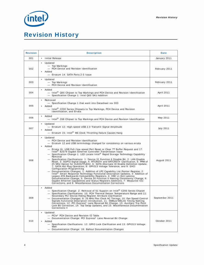
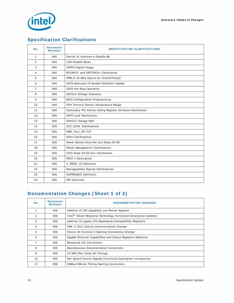
Removal— Specification Clarifications: 1: Device 31 Function 6 Disable Bit, 2: LAN Disable
Reset, 3: SGPIO Signal Usage, 4: RTCRST# and SRTCRST# Clarification, 5: PPM of 25 MHz Option for CLKOUTFLEX2, 6: SATA Alternate ID Enable Definition Update, 7: SATA Hot Plug Operation, 8: GPIO13 Voltage Tolerance, and 9: EHCI Configuration Programming
— Documentation Changes: 1: Addition of LPC Capability List Pointer Register, 2: Intel® Smart Response Technology Functional Description Updates, 3: Addition of Legacy ATA Backwards Compatibility Registers, 4: DMI L1 Exit Latency Documentation Change, 5: Device 30 Function 0 Naming Consistency Change, 6: Gigabit Ethernet Capabilities and Status Registers Additions, 7: Measured ICC Corrections, and 8: Miscellaneous Documentation Corrections
August 2011
009
• Added — Specification Change: 2: Removal of S1 Support on Intel® C200 Series Chipset— Specification Clarifications: 10: PCH Thermal Sensor Temperature Range and 11:
Secondary PCI Device Hiding Register Attribute Clarification— Documentation Changes: 9: 25 MHz Flex Clock AC Timings, 10: Fan Speed Control
Signals Functional Description Introduction, 11: SMBus/SMLink Timing Naming Corrections, 12: PCI Express* Lane Reversal Bit Change, 13: Auxiliary Trip Point Lock Bit Correction, 14: Top Swap Updates, and 15: Miscellaneous Documentation Corrections II
September 2011
010
• Updated— PCIe* PCH Device and Revision ID Table— Documentation Change: PCI Express* Lane Reversal Bit Change
• Added — Specification Clarifications: 12: GPIO Lock Clarification and 13: GPIO13 Voltage
This document is an update to the specifications contained in the Affected Documents/Related Documents table below. This document is a compilation of device and documentation errata, specification clarifications and changes. It is intended for hardware system manufacturers and software developers of applications, operating systems, or tools.
Information types defined in Nomenclature are consolidated into the specification update and are no longer published in other documents.
This document may also contain information that was not previously published.
Affected Documents/Related Documents
NomenclatureErrata are design defects or errors. Errata may cause the behavior of the PCH to deviate from published specifications. Hardware and software designed to be used with any given stepping must assume that all errata documented for that stepping are present in all devices.
Specification Changes are modifications to the current published specifications. These changes will be incorporated in any new release of the specification.
Specification Clarifications describe a specification in greater detail or further highlight a specification’s impact to a complex design situation. These clarifications will be incorporated in any new release of the specification.
Documentation Changes include typos, errors, or omissions from the current published specifications. These will be incorporated in any new release of the specification.
§ §
Title Document Number
Intel® 6 Series Chipset and Intel® C200 Series Chipset Datasheet 324645-006
Summary Tables of Changes
8 Specification Update
Summary Tables of Changes
The following tables indicate the errata, specification changes, specification clarifications, or documentation changes which apply to the product. Intel may fix some of the errata in a future stepping of the component and account for the other outstanding issues through documentation or specification changes as noted. These tables use the following notations:
Codes Used in Summary Tables
SteppingX: Erratum exists in the stepping indicated. Specification Change
that applies to this stepping.
(No mark)
or (Blank box): This erratum is fixed or not applicable in listed stepping or Specification Change does not apply to listed stepping.
StatusDoc: Document change or update will be implemented.
Plan Fix: This erratum may be fixed in a future stepping of the product.
Fixed: This erratum has been previously fixed.
No Fix: There are no plans to fix this erratum.
RowChange bar to left of table row indicates this erratum is either new or modified from the previous version of the document.
Specification Update 9
Summary Tables of Changes
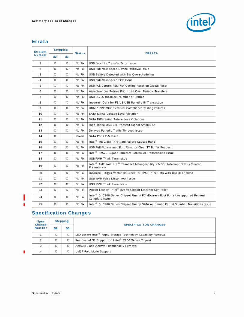
Errata
Erratum Number
SteppingStatus ERRATA
B2 B3
1 X X No Fix USB Isoch In Transfer Error Issue
2 X X No Fix USB Full-/low-speed Device Removal Issue
3 X X No Fix USB Babble Detected with SW Overscheduling
4 X X No Fix USB Full-/low-speed EOP Issue
5 X X No Fix USB PLL Control FSM Not Getting Reset on Global Reset
6 X X No Fix Asynchronous Retries Prioritized Over Periodic Transfers
7 X X No Fix USB FS/LS Incorrect Number of Retries
8 X X No Fix Incorrect Data for FS/LS USB Periodic IN Transaction
9 X X No Fix HDMI* 222 MHz Electrical Compliance Testing Failures
10 X X No Fix SATA Signal Voltage Level Violation
11 X X No Fix SATA Differential Return Loss Violations
12 X X No Fix High-speed USB 2.0 Transmit Signal Amplitude
13 X X No Fix Delayed Periodic Traffic Timeout Issue
14 X Fixed SATA Ports 2-5 Issue
15 X X No Fix Intel® ME Clock Throttling Failure Causes Hang
16 X X No Fix USB Full-/Low-speed Port Reset or Clear TT Buffer Request
17 X X No Fix Intel® 82579 Gigabit Ethernet Controller Transmission Issue
18 X X No Fix USB RMH Think Time Issue
19 X X No Fix Intel® AMT and Intel® Standard Manageability KT/SOL Interrupt Status Cleared Prematurely
20 X X No Fix Incorrect IRQ(x) Vector Returned for 8259 Interrupts With RAEOI Enabled
21 X X No Fix USB RMH False Disconnect Issue
22 X X No Fix USB RMH Think Time Issue
23 X X No Fix Packet Loss on Intel® 82579 Gigabit Ethernet Controller
24 X X No Fix Intel® 6/ C200 Series Chipset Family PCI-Express Root Ports Unsupported Request Complete Issue
25 X X No Fix Intel® 6/ C200 Series Chipset Family SATA Automatic Partial Slumber Transitions Issue
Specification ChangesSpec
Change Number
SteppingSPECIFICATION CHANGES
B2 B3
1 X X LED Locate Intel® Rapid Storage Technology Capability Removal
2 X X Removal of S1 Support on Intel® C200 Series Chipset
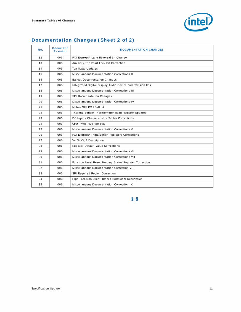
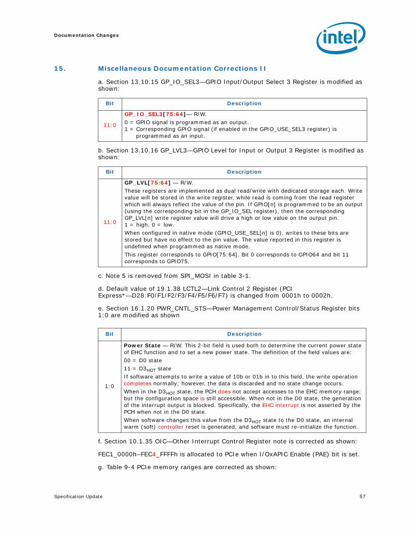
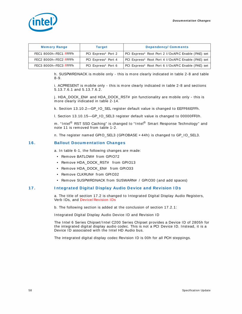
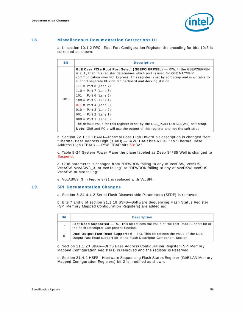
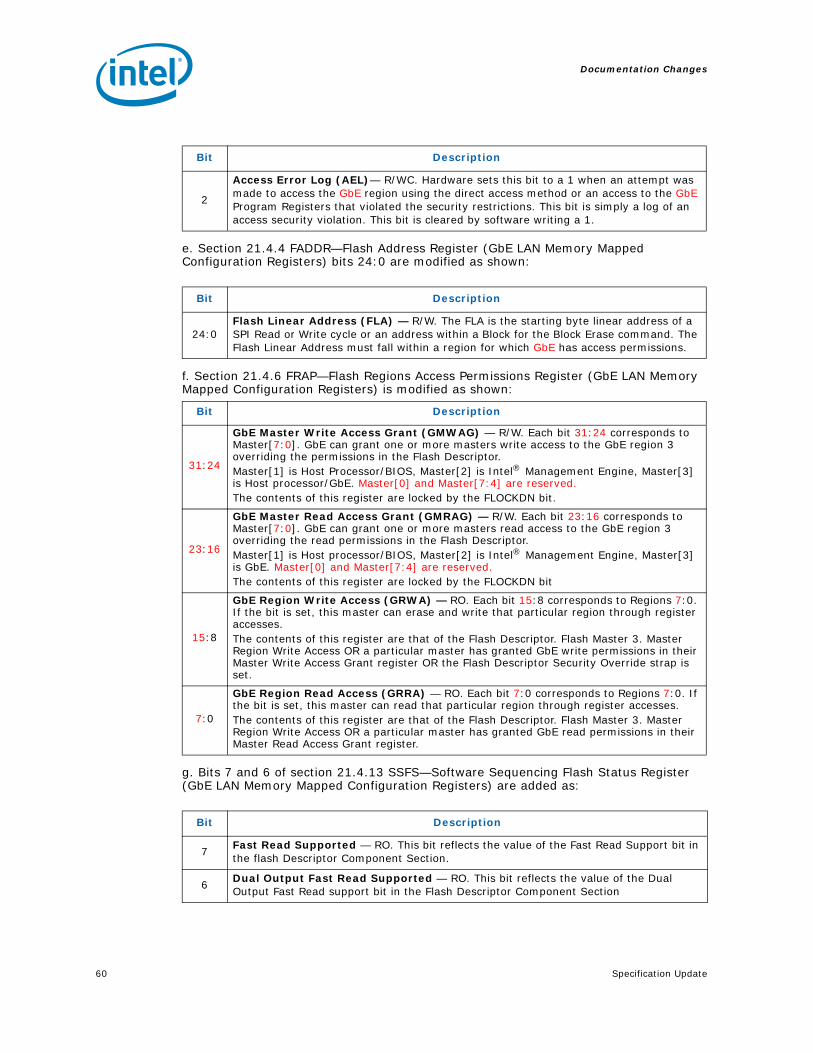
30 006 Miscellaneous Documentation Corrections VII
31 006 Function Level Reset Pending Status Register Correction
32 006 Miscellaneous Documentation Correction VIII
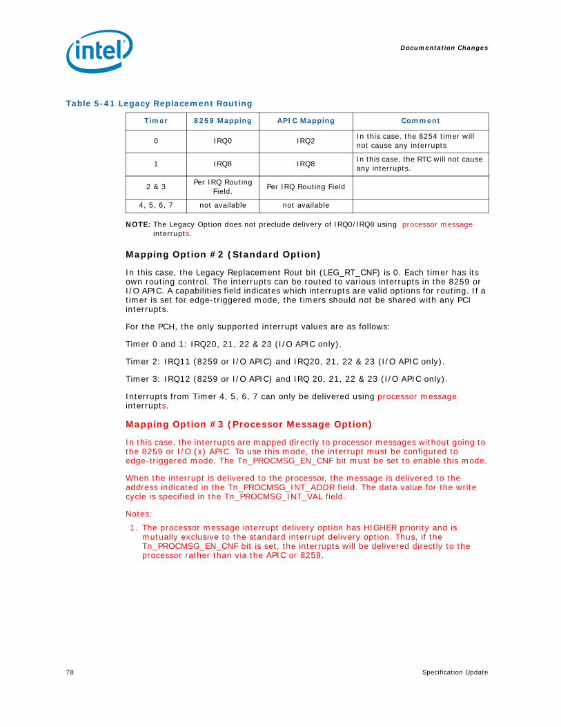
33 006 SPI Required Region Correction
34 006 High Precision Event Timers Functional Description
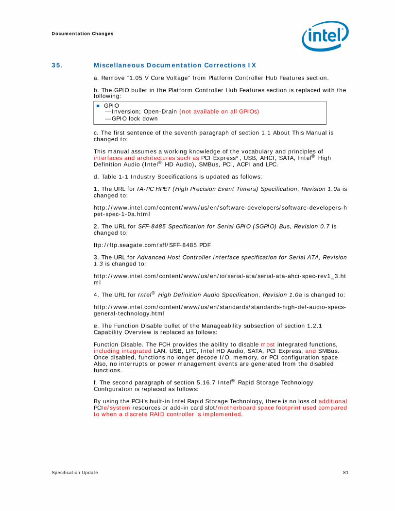
35 006 Miscellaneous Documentation Correction IX
Documentation Changes (Sheet 2 of 2)
No. DocumentRevision DOCUMENTATION CHANGES
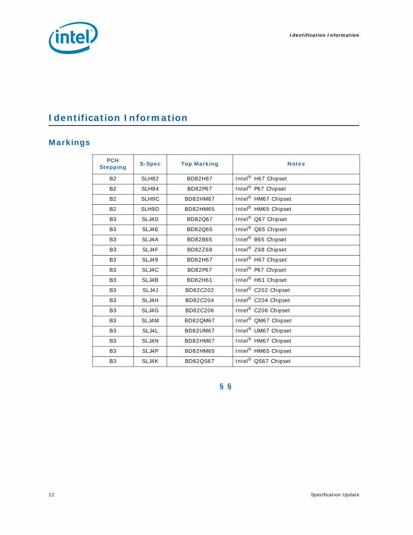
Identification Information
12 Specification Update
Identification Information
Markings
§ §
PCH Stepping S-Spec Top Marking Notes
B2 SLH82 BD82H67 Intel® H67 Chipset
B2 SLH84 BD82P67 Intel® P67 Chipset
B2 SLH9C BD82HM67 Intel® HM67 Chipset
B2 SLH9D BD82HM65 Intel® HM65 Chipset
B3 SLJ4D BD82Q67 Intel® Q67 Chipset
B3 SLJ4E BD82Q65 Intel® Q65 Chipset
B3 SLJ4A BD82B65 Intel® B65 Chipset
B3 SLJ4F BD82Z68 Intel® Z68 Chipset
B3 SLJ49 BD82H67 Intel® H67 Chipset
B3 SLJ4C BD82P67 Intel® P67 Chipset
B3 SLJ4B BD82H61 Intel® H61 Chipset
B3 SLJ4J BD82C202 Intel® C202 Chipset
B3 SLJ4H BD82C204 Intel® C204 Chipset
B3 SLJ4G BD82C206 Intel® C206 Chipset
B3 SLJ4M BD82QM67 Intel® QM67 Chipset
B3 SLJ4L BD82UM67 Intel® UM67 Chipset
B3 SLJ4N BD82HM67 Intel® HM67 Chipset
B3 SLJ4P BD82HM65 Intel® HM65 Chipset
B3 SLJ4K BD82QS67 Intel® QS67 Chipset
Specification Update 13
PCH Device and Revision Identification
PCH Device and Revision Identification
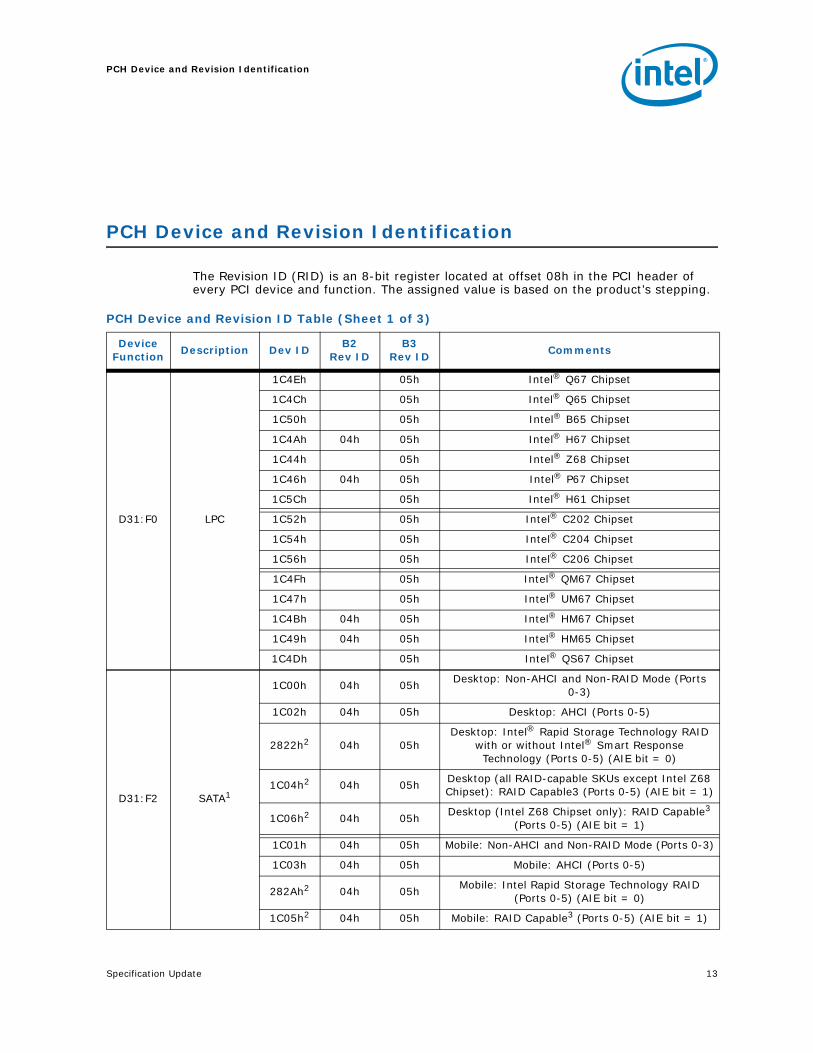
The Revision ID (RID) is an 8-bit register located at offset 08h in the PCI header of every PCI device and function. The assigned value is based on the product’s stepping.
PCH Device and Revision ID Table (Sheet 1 of 3)
Device Function Description Dev ID B2
Rev IDB3
Rev ID Comments
D31:F0 LPC
1C4Eh 05h Intel® Q67 Chipset
1C4Ch 05h Intel® Q65 Chipset
1C50h 05h Intel® B65 Chipset
1C4Ah 04h 05h Intel® H67 Chipset
1C44h 05h Intel® Z68 Chipset
1C46h 04h 05h Intel® P67 Chipset
1C5Ch 05h Intel® H61 Chipset
1C52h 05h Intel® C202 Chipset
1C54h 05h Intel® C204 Chipset
1C56h 05h Intel® C206 Chipset
1C4Fh 05h Intel® QM67 Chipset
1C47h 05h Intel® UM67 Chipset
1C4Bh 04h 05h Intel® HM67 Chipset
1C49h 04h 05h Intel® HM65 Chipset
1C4Dh 05h Intel® QS67 Chipset
D31:F2 SATA1
1C00h 04h 05h Desktop: Non-AHCI and Non-RAID Mode (Ports 0-3)
1C10h B4h B5h Desktop and Mobile (When D28:F0:ECh:bit 1= 0)
244Eh B4h B5h Desktop (When D28:F0:ECh:bit 1 = 1)
2448h B4h B5h Mobile (When D28:F0:ECh:bit 1 = 1)
D28:F1 PCI Express Port 2
1C12h B4h B5h Desktop and Mobile (When D28:F1:ECh:bit 1 = 0)
244Eh B4h B5h Desktop (When D28:F1:ECh:bit 1 = 1)
2448h B4h B5h Mobile (When D28:F1:ECh:bit 1 = 1)
D28:F2 PCI Express Port 3
1C14h B4h B5h Desktop and Mobile (When D28:F2:ECh:bit 1 = 0)
244Eh B4h B5h Desktop (When D28:F2:ECh:bit 1 = 1)
2448h B4h B5h Mobile (When D28:F2:ECh:bit 1 = 1)
D28:F3 PCI Express Port 4
1C16h B4h B5h Desktop and Mobile (When D28:F3:ECh:bit 1 = 0)
244Eh B4h B5h Desktop (When D28:F3:ECh:bit 1 = 1)
2448h B4h B5h Mobile (When D28:F3:ECh:bit 1 = 1)
D28:F4 PCI Express Port 5
1C18h B4h B5h Desktop and Mobile (When D28:F4:ECh:bit 1 = 0)
244Eh B4h B5h Desktop (When D28:F4:ECh:bit 1 = 1)
2448h B4h B5h Mobile (When D28:F4:ECh:bit 1 = 1)
D28:F5 PCI Express Port 6
1C1Ah B4h B5h Desktop and Mobile (When D28:F5:ECh:bit 1 = 0)
244Eh B4h B5h Desktop (When D28:F5:ECh:bit 1 = 1)
2448h B4h B5h Mobile (When D28:F5:ECh:bit 1 = 1)
D28:F6 PCI Express Port 7
1C1Ch B4h B5h Desktop and Mobile (When D28:F6:ECh:bit 1 = 0)
244Eh B4h B5h Desktop (When D28:F6:ECh:bit 1 = 1)
2448h B4h B5h Mobile (When D28:F6:ECh:bit 1 = 1)
D28:F7 PCI Express Port 8
1C1Eh B4h B5h Desktop and Mobile (When D28:F7:ECh:bit 1 = 0)
244Eh B4h B5h Desktop (When D28:F7:ECh:bit 1 = 1)
2448h B4h B5h Mobile (When D28:F7:ECh:bit 1 = 1)
PCH Device and Revision ID Table (Sheet 2 of 3)
Device Function Description Dev ID B2
Rev IDB3
Rev ID Comments
Specification Update 15
PCH Device and Revision Identification
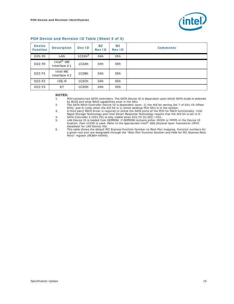
NOTES:1. PCH contains two SATA controllers. The SATA Device ID is dependent upon which SATA mode is selected
by BIOS and what RAID capabilities exist in the SKU.2. The SATA RAID Controller Device ID is dependent upon: 1) the AIE bit setting (bit 7 of D31:F2:Offset
9Ch); and 2) (only when the AIE bit is 1) which desktop PCH SKU is in the system.3. A third party RAID driver is required to utilize the SATA ports of the PCH for RAID functionality. Intel
Rapid Storage Technology and Intel Smart Response Technology require that the AIE bit is set to 0.4. SATA Controller 2 (D31:F5) is only visible when D31:F2 CC.SCC =01h.5. LAN Device ID is loaded from EEPROM. If EEPROM contains either 0000h or FFFFh in the Device ID
location, then 1C33h is used. Refer to the appropriate Intel® GbE physical layer Transceiver (PHY) datasheet for LAN Device IDs.
6. This table shows the default PCI Express Function Number-to-Root Port mapping. Function numbers for a given root port are assignable through the “Root Port Function Number and Hide for PCI Express Root Ports” register (RCBA+0404h).
D25:F0 LAN 1C33h5 04h 05h
D22:F0 Intel® ME Interface #1 1C3Ah 04h 05h
D22:F1 Intel ME Interface #2 1C3Bh 04h 05h
D22:F2 IDE-R 1C3Ch 04h 05h
D22:F3 KT 1C3Dh 04h 05h
PCH Device and Revision ID Table (Sheet 3 of 3)
Device Function Description Dev ID B2
Rev IDB3
Rev ID Comments
Errata
16 Specification Update
Errata
1. USB Isoch In Transfer Error IssueProblem: If a USB full-speed inbound isochronous transaction with a packet length 190 bytes or
greater is started near the end of a microframe the PCH may see more than 189 bytes in the next microframe.
Implication: If the PCH sees more than 189 bytes for a microframe an error will be sent to software and the isochronous transfer will be lost. If a single data packet is lost no perceptible impact for the end user is expected.
Note: Intel has only observed the issue in a synthetic test environment where precise control of packet scheduling is available, and has not observed this failure in its compatibility validation testing.
• Isochronous traffic is periodic and cannot be retried thus it is considered good practice for software to schedule isochronous transactions to start at the beginning of a microframe. Known software solutions follow this practice.
• To sensitize the system to the issue additional traffic such as other isochronous transactions or retries of asynchronous transactions would be required to push the inbound isochronous transaction to the end of the microframe.
Workaround: None.Status: No Plan to Fix.
2. USB Full-/low-speed Device Removal IssueProblem: If two or more USB full-/low-speed devices are connected to the same USB controller,
the devices are not suspended, and one device is removed, one or more of the devices remaining in the system may be affected by the disconnect.
Implication: The implication is device dependent. A device may experience a delayed transaction, stall and be recovered via software, or stall and require a reset such as a hot plug to resume normal functionality.
Workaround: None.Status: No Plan to Fix.
Specification Update 17
Errata
3. USB Babble Detected with SW OverschedulingProblem: If software violates USB periodic scheduling rules for full-speed isochronous traffic by
overscheduling, the RMH may not handle the error condition properly and return a completion split with more data than the length expected.
Implication: If the RMH returns more data than expected, the endpoint will detect packet babble for that transaction and the packet will be dropped. Since overscheduling occurred to create the error condition, the packet would be dropped regardless of RMH behavior. If a single isochronous data packet is lost, no perceptible impact to the end user is expected.
Note: USB software overscheduling occurs when the amount of data scheduled for a microframe exceeds the maximum budget. This is an error condition that violates the USB periodic scheduling rule.
Note: This failure has only been recreated synthetically with USB software intentionally overscheduling traffic to hit the error condition.
Workaround: None.Status: No Plan to Fix.
4. USB Full-/low-speed EOP IssueProblem: If the EOP of the last packet in a USB Isochronous split transaction (Transaction >189
bytes) is dropped or delayed 3 ms or longer the following may occur:• If there are no other pending low-speed or full-speed transactions the RMH will not
send SOF, or Keep-Alive. Devices connected to the RMH will interpret this condition as idle and will enter suspend.
• If there is other pending low-speed or full-speed transactions, the RMH will drop the isochronous transaction and resume normal operation.
Implication:• If there are no other transactions pending, the RMH is unaware a device entered
suspend and may starting sending a transaction without waking the device. The implication is device dependent, but a device may stall and require a reset to resume functionality.
• If there are other transactions present, only the initial isochronous transaction may be lost. The loss of a single isochronous transaction may not result in end user perceptible impact.
Note: Intel has only observed this failure when using software that does not comply with the USB specification and violates the hardware isochronous scheduling threshold by terminating transactions that are already in progress.
Workaround: None.Status: No Plan to Fix.
5. USB PLL Control FSM not Getting Reset on Global ResetProblem: Intel® 6 Series Chipset and Intel® C200 Series Chipset USB PLL may not lock if a
Global Reset occurs early during a cold boot sequence.Implication: USB interface would not be functional an additional cold boot would be necessary to
recover.Workaround: None.Status: No Plan to Fix.
Errata
18 Specification Update
6. Asynchronous Retries Prioritized Over Periodic TransfersProblem: The integrated USB RMH incorrectly prioritizes full-speed and low-speed asynchronous
retries over dispatchable periodic transfers.Implication: Periodic transfers may be delayed or aborted. If the asynchronous retry latency causes
the periodic transfer to be aborted, the impact varies depending on the nature of periodic transfer:
• If a periodic interrupt transfer is aborted, the data may be recovered by the next instance of the interrupt or the data could be dropped.
• If a periodic isochronous transfer is aborted, the data will be dropped. A single dropped periodic transaction should not be noticeable by end user.
Note: This issue has only been seen in a synthetic environment. The USB spec does not consider the occasional loss of periodic traffic a violation.
Workaround: None.Status: No Plan to Fix.
7. USB FS/LS Incorrect Number of RetriesProblem: A USB low-speed Transaction may be retried more than three times, and a USB
full-speed transaction may be retried less than three times if all of the following conditions are met:
• A USB low-speed transaction with errors, or the first retry of the transaction occurs near the end of a microframe, and there is not enough time to complete another retry of the low-speed transaction in the same microframe.
• There is pending USB full-speed traffic and there is enough time left in the microframe to complete one or more attempts of the full-speed transaction.
• Both the low-speed and full-speed transactions must be asynchronous (Bulk/Control) and must have the same direction either in or out.
Note: Note: Per the USB EHCI Specification a transaction with errors should be attempted a maximum of 3 times if it continues to fail.
Implication:• For low-speed transactions the extra retry(s) allow a transaction additional
chance(s) to recover regardless of if the full-speed transaction has errors or not.• If the full-speed transactions also have errors, the PCH may retry the transaction
fewer times than required, stalling the device prematurely. Once stalled, the implication is software dependent, but the device may be reset by software.
Workaround: None.Status: No Plan to Fix.
Specification Update 19
Errata
8. Incorrect Data for FS/LS USB Periodic IN TransactionProblem: The Periodic Frame list entry in DRAM for a USB FS or LS Periodic IN transaction may
incorrectly get some of its data from a prior Periodic IN transaction which was initiated very late into the preceding microframe.
It is considered good practice for software to schedule Periodic Transactions at the start of a microframe. However Periodic transactions may occur late into a microframe due to the following cases outlined below:
• Asynchronous transaction starting near the end of the proceeding microframe gets Asynchronously retried.
Note: Transactions getting Asynchronous retried would only occur for ill behaved USB device or USB port with a signal integrity issue
• Or Two Periodic transactions are scheduled by software to occur in the same microframe and the first needs to push the second Periodic IN transaction to the end of the microframe boundary.
Implication: The implication will be device, driver or operating system specific.
Note: This issue has only been observed in a synthetic test environment.Workaround: None.Status: No Plan to Fix.
9. HDMI* 222 MHz Electrical Compliance Testing FailuresProblem: HDMI* 222 MHz electrical compliance testing may show eye diagram and jitter test
failures on Intel 6 Series Chipset and Intel C200 Series Chipset.Implication: No functional or visual failures have been observed by Intel. HDMI electrical compliance
failures may be seen at 222 MHz Deep Color Mode. This issue does not prevent HDMI with Deep Color Logo certification as no failures have been seen with 74.25 MHz Deep Color Mode (720P 60 Hz or 1080P 30 Hz) as required HDMI Compliance Test Specification.
Workaround: None.Status: No Plan to Fix.
10. SATA Signal Voltage Level ViolationProblem: SATA transmit buffers have been designed to maximize performance and robustness
over a variety of routing scenarios. As a result, the SATA transmit signaling voltage levels may exceed the maximum motherboard TX connector and device RX connector voltage specifications as defined in section 7.2.1 of the Serial ATA specification, rev 3.0. This issue applies to Gen 1 (1.5 Gb/s) and Gen 2 (3.0 Gb/s).
Implication: None known.Workaround: None.Status: No Plan to Fix.
Errata
20 Specification Update
11. SATA Differential Return Loss ViolationsProblem: The Intel 6 Series Chipset and Intel C200 Series Chipset SATA buffer capacitance may
be higher than expected.Implication: There are no known functional failures. This may cause a violation of the SATA-IO*
compliance test for Receiver or Transmitter Differential Return Loss.Workaround: None.
Note: Intel has obtained a waiver for the SATA-IO building block status.Status: No Plan to Fix.
12. High-speed USB 2.0 Transmit Signal AmplitudeProblem: Intel 6 Series Chipset and Intel C200 Series Chipset High-speed USB 2.0 transmit
signal amplitude may exceed the USB 2.0 specification.• USB 2.0 Specification Transmit Eye template maximum boundary is +/- 525 mV
following bit transitions and +/- 475 mV for non-transitional bit patterns.• USB 2.0 Specification VHSOH maximum is 440 mV.
Implication: There are no known functional failures.Workaround: None.Status: No Plan to Fix.
13. Delayed Periodic Traffic Timeout IssueProblem: If a periodic interrupt transaction is pushed out to the x+4 microframe boundary, the
RMH may not wait for the transaction to timeout before starting the next transaction.Implication: If the next full-speed or low-speed transaction is intended for the same device targeted
by the periodic interrupt, the successful completion of that transaction is device dependent and cannot be guaranteed. The implication may differ depending on the nature of the transaction:
• If the transaction is asynchronous and the device does not respond, it will eventually be retried with no impact.
• If the transaction is periodic and the device does not respond, the transfer may be dropped. A single dropped periodic transaction should not be noticeable by end user.
Note: This issue has only been seen in a synthetic environment.Workaround: None.Status: No Plan to Fix.
Specification Update 21
Errata
14. SATA Ports 2-5 IssueProblem: Due to a circuit design issue on Intel 6 Series Chipset and Intel C200 Series Chipset,
electrical lifetime wear out may affect clock distribution for SATA ports 2-5. This may manifest itself as a functional issue on SATA ports 2-5 over time.
• The electrical lifetime wear out may result in device oxide degradation which over time can cause drain to gate leakage current.
• This issue has time, temperature and voltage sensitivities.Implication: The increased leakage current may result in an unstable clock and potentially functional
issues on SATA ports 2-5 in the form of receive errors, transmit errors, and unrecognized drives.
• Data saved or stored prior to functional issues on a SATA device will be retrievable if connected to a working SATA port.
• SATA ports 0-1 are not affected by this design issue as they have separate clock generation circuitry.
Workaround: Intel has worked with board and system manufacturers to identify and implement solutions for affected systems.
• Use only SATA ports 0-1.• Use an add-in PCIe SATA bridge solution.
Status: Fixed. For steppings affected, see the Summary Table of Changes.• This issue has been resolved with a silicon stepping for all Intel 6 Series Chipset
and Intel C200 Series Chipset incorporating a minor metal layer change.• The fix does not impact the designed functionality and electrical specifications of
the Intel 6 Series Chipset and Intel C200 Series Chipset.
15. Intel® ME Clock Throttling Failure Causes HangProblem: When the Intel® Management Engine (Intel® ME) firmware sets the internal clock
frequency, the Intel ME clock may stop toggling, potentially causing the Intel®Management Engine Interface to become unresponsive.
Implication: Parts that exhibit this issue may hang during POST.
Note: No functional failures have been seen due to this issue.Workaround: An Intel® ME Firmware code change has been identified and may be implemented as a
workaround for this erratum.Status: No Plan to Fix.
Errata
22 Specification Update
16. USB Full-/Low-speed Port Reset or Clear TT Buffer RequestProblem: One or more full-/low-speed USB devices on the same RMH controller may be affected
if the devices are not suspended and either (a) software issues a Port Reset OR (b) software issues a Clear TT Buffer request to a port executing a split full-/low-speed Asynchronous Out command.
• The Small window of exposure for full-speed device is around 1.5 microseconds and around 12 microseconds for a low-speed device.
Implication: The affected port may stall or receive stale data for a newly arrived split transfer occurring at the time of the Port Reset or Clear TT Buffer request.
Note: This issue has only been observed in a synthetic test environment.Workaround: None.Status: No Plan to Fix.
17. Intel® 82579 Gigabit Ethernet Controller Transmission IssueProblem: Intel® 82579 Gigabit Ethernet Controller with the Intel 6 Series Chipset and Intel C200
Series Chipset and Intel ME Firmware 7.x 5 MB may stop transmitting during a data transfer.
Implication: Intel 82579 Gigabit Ethernet Controller may stop transmitting packets, the link LED will blink, and a power cycle may be required to resume transmission activity.
Note: This issue has only been observed in a focused test environment where data is constantly transferred over an extended period of time (more than approximately 3 hours).
Workaround: A combination of Intel ME Firmware code change and Intel 82579 Gigabit Ethernet Controller LAN Driver update has been identified and may be implemented as a workaround for this erratum.
Status: No Plan to Fix.
18. USB RMH Think Time IssueProblem: The Intel 6 Series Chipset and Intel C200 Series Chipset USB RMH Think Time may
exceed its declared value in the RMH hub descriptor register of 8 full-speed bit times. Implication: If the OS USB driver fully subscribes a USB microframe, full-/low-speed transactions
may exceed the microframe boundary.
Note: No functional failures have been observed.Workaround: None.Status: No Plan to Fix.
Specification Update 23
Errata
19. Intel® AMT and Intel® Standard Manageability KT/SOL Interrupt Status Cleared Prematurely
Problem: A read of the Intel® AMT and Intel® Standard Manageability enabled SOL KTIIR (KT Interrupt Identification Register) or KTLSR (KT Line Status Register) that occurs simultaneous to the arrival of an SOL Host interrupt event may result in a read of the Interrupt Status (INTSTS) bit 0 returning the status of “No Pending interrupt to Host” despite KTLSR reporting a serviceable event.
Implication: Implication of a missed SOL Host interrupt is software implementation dependent. Subsequent interrupts not aligned to a KTIIR or KTLSR read will clear “0” bit 0 (INTSTS) to indicate a pending interrupt to the Host.
Workaround: Software should not rely on reading only bit 0 (INTSTS) of the KTIIR register and should also poll the KTLSR to determine if a SOL Host interrupt is pending.
Status: No Plan to Fix.
20. Incorrect IRQ(x) Vector Returned for 8259 Interrupts With RAEOI Enabled
Problem: If multiple interrupts are active prior to an interrupt acknowledge cycle with Rotating Automatic End of Interrupt (RAEOI) mode of operation enabled for 8259 interrupts (0-7), an incorrect IRQ(x) vector may be returned to the processor.
Implication: Implications of an incorrect IRQ(x) vector being returned to the CPU are SW implementation dependent.
Note: This issue has only been observed in a synthetic test environment.Workaround: None.Status: No Plan to Fix.
21. USB RMH False Disconnect IssueProblem: The PCH may falsely detect a USB High-Speed (HS) device disconnect if all of the
following conditions are met:• The HS Device is connected through the Rate Matching Hub (RMH) of the PCH’s
EHCI controller. • The device is resuming from selective suspend or port reset.• The resume occurs within a narrow time window during the EOP (End of Packet)
portion of the SOF (Start of Frame) Packet on the USB bus.Implication: Following the false disconnect, the HS device will be automatically re-enumerated. The
system implication will depend on the resume event cause:• If the resume event is a port reset, a second port reset will be automatically
generated and the device re-enumerated. No end user impact is expected.• If the resume event is a hardware or software initiated resume from selective
suspend, the implication will be device and software specific, which may result in anomalous system behavior.
Note: If the HS device is a hub, then all of the devices behind the hub, independent of the device speed, may also be re-enumerated.
Workaround: None.Status: No Plan to Fix.
Errata
24 Specification Update
22. USB RMH Think Time IssueProblem: The USB RMH Think Time may exceed its declared value in the RMH hub descriptor
register of 8 full-speed bit times. Implication: If the USB driver fully subscribes a USB microframe, LS/FS transactions may exceed
the microframe boundary.
Note: No functional failures have been observed.Workaround: None.Status: No Plan to Fix.
23. Packet Loss on Intel® 82579 Gigabit Ethernet ControllerProblem: Systems with Intel 6 Series Chipset and Intel C200 Series Chipset using the Intel
82579 Gigabit Ethernet Controller may experience packet Loss at 100 Mbps and 1 Gbps speeds when the link between the Intel 82579 Gigabit Ethernet Controller and the PCH Integrated LAN Controller is exiting the Low Power Link (K1) State.
Implication: Implications are application and Internet Protocol dependent.Workaround: A BIOS code change has been identified and may be implemented as a workaround for
this erratum.Status: No Plan to Fix.
24. Intel® 6/ C200 Series Chipset Family PCI-Express Root Ports Unsupported Request Complete Issue
Problem: Intel® 6 / C200 Series Chipset Family PCI-Express Root Ports in receipt of a Memory Read TLP may return a Unsupported Request (UR) Completion with an incorrect lower address field if any of the following are true:
Bus Master Enable is disabled in the PCI-Express Root Port's Command register (PCICMD bit2 =0)
• AT field of the TLP header is non-zero.• The requested upstream address falls within the memory range claimed by the
secondary side of the bridge.• Requester ID with Bus Number of 0.
Implication: The UR Completion with an incorrect lower address field may be handled as a malformed TLP by the requestor causing an ERR_NONFATAL or ERR_FATAL message to be sent upstream to the root port. System level implication is dependent on platform error handling configuration.
Note: The message type sent by the requestor will depend on the requestor's severity setting for a malformed TLP in the Uncorrectable Error Severity Register (UEV).
Workaround: None.Status: No Plan to Fix.
25. Intel® 6 / C200 Series Chipset Family SATA Automatic Partial Slumber Transitions Issue
Problem: Intel® 6 / C200 Series Chipset Family SATA Automatic Partial Slumber Transitions (APST) feature may prevent internal clock gating when SATA Ports transition from Partial to Slumber state.
Implication: For platforms implementing APST, power savings maybe less than expected when SATA port(s) are in the slumber state.
Specification Update 25
Errata
Workaround: Software should not enable Automatic Partial Slumber Transitions for both the SATA Host controller and SATA Devices supporting APST. Intel® Rapid Storage Technology (Intel® RST) Driver version 11.5 or later does not enable APST.
Note: Active to Slumber transitions are still supported with APST disabled, maintaining power savings due to clock gating when in Slumber.
Bit 7 of 14.4.1.10 RSTF—Intel® RST Feature Capabilities Register (ABAR + C8h–C9h), previously known as the LED Locate (LEDL) bit, is changed to Reserved.
2. Removal of S1 Support on Intel® C200 Series Chipset
The S1 power state is no longer supported for the Intel® C200 Series Chipset. The change is made accordingly in the Datasheet.
3. A20GATE and A20M# Functionality Removal
A20M# functionality is not supported on processors on Intel® 6 Series Chipset and Intel C200 Series Chipset-based platforms.
a. Table 2-9 is updated as shown:
b. Table 3-4 is updated as shown:
c. Table 3-5 is updated as shown:
d. A20M# is removed as a VLW message from section 5.12.
e. Section 5.12.1.1 is removed.
f. A20GATE/A20M# removed from section 5.12.2.1.
g. A20M# removed from section 5.12.3.
Name Type Description
A20GATE I A20 Gate: Functionality reserved. A20M# functionality is not supported.
Signal Name Power Well Driver During Reset S0/S1 S3 S4/S5
Processor Interface
A20GATE Core External Micro controller or Pull-up Static Off Off
Signal Name Power Well Driver During Reset C-x states S0/S1 S3 S4/S5
Processor Interface
A20GATE Core External Micro controller or Pull-up Static Static Off Off
Specification Update 27
Specification Changes
h. 13.1.27 ULKMC — USB Legacy Keyboard / Mouse Control Register bit 5 is modified as shown:
i. Section 13.7.3 name changed from PORT92—Fast A20 and Init Register to PORT92—Init Register and bit 1 is modified as shown:
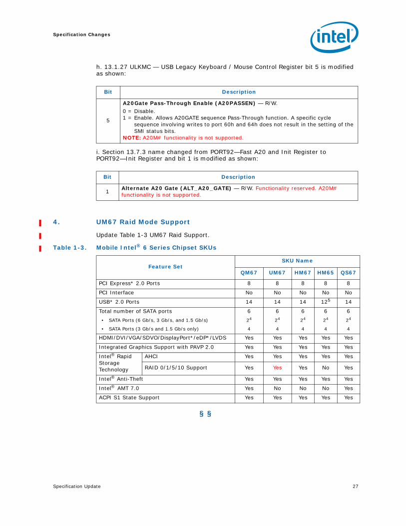
4. UM67 Raid Mode Support
Update Table 1-3 UM67 Raid Support.
Table 1-3. Mobile Intel® 6 Series Chipset SKUs
§ §
Bit Description
5
A20Gate Pass-Through Enable (A20PASSEN) — R/W.0 = Disable.1 = Enable. Allows A20GATE sequence Pass-Through function. A specific cycle
sequence involving writes to port 60h and 64h does not result in the setting of the SMI status bits.
NOTE: A20M# functionality is not supported.
Bit Description
1 Alternate A20 Gate (ALT_A20_GATE) — R/W. Functionality reserved. A20M# functionality is not supported.
Feature SetSKU Name
QM67 UM67 HM67 HM65 QS67
PCI Express* 2.0 Ports 8 8 8 8 8
PCI Interface No No No No No
USB* 2.0 Ports 14 14 14 125 14
Total number of SATA ports 6 6 6 6 6• SATA Ports (6 Gb/s, 3 Gb/s, and 1.5 Gb/s) 24 24 24 24 24
Integrated Graphics Support with PAVP 2.0 Yes Yes Yes Yes Yes
Intel® Rapid Storage Technology
AHCI Yes Yes Yes Yes Yes
RAID 0/1/5/10 Support Yes Yes Yes No Yes
Intel® Anti-Theft Yes Yes Yes Yes Yes
Intel® AMT 7.0 Yes No No No Yes
ACPI S1 State Support Yes Yes Yes Yes Yes
Specification Clarifications
28 Specification Update
Specification Clarifications
1. Device 31 Function 6 Disable Bit
Section 10.1.45 FD—Function Disable Register bit 24 is changed as shown:
2. LAN Disable Reset
Section 10.1.44 BUC—Backed Up Control Register bit 5 is changed as shown:
3. SGPIO Signal Usage
The following note is added at the conclusion of the first paragraph of section 5.16.13:
Intel does not validate all possible usage cases of this feature. Customers should validate their specific design implementation on their own platforms.
4. RTCRST# and SRTCRST# Clarification
The following replaces section 5.13.10.6:
RTCRST# is used to reset PCH registers in the RTC Well to their default value. If a jumper is used on this pin, it should only be pulled low when system is in the G3 state and then replaced to the default jumper position. Upon booting, BIOS should recognize that RTCRST# was asserted and clear internal PCH registers accordingly. It is imperative that this signal not be pulled low in the S0 to S5 states.
SRTCRST# is used to reset portions of the Intel Management Engine and should not be connected to a jumper or button on the platform. The only time this signal gets asserted (driven low in combination with RTCRST#) should be when the coin cell battery is removed or not installed and the platform is in the G3 state. Pulling this
Bit Description
24Thermal Sensor Registers Disable (TTD) — R/W. Default is 0.0 = Thermal Sensor Registers (D31:F6) are enabled.1 = Thermal Sensor Registers (D31:F6) are disabled.
Bit Description
5
LAN Disable — R/W.0 = LAN is Enabled1 = LAN is Disabled.Changing the internal GbE controller from disabled to enabled requires a system reset (write of 0Eh to CF9h (RST_CNT Register)) immediately after clearing the LAN disable bit. A reset is not required if changing the bit from enabled to disabled.This bit is locked by the Function Disable SUS Well Lockdown register. Once locked, this bit cannot be changed by software.
Specification Update 29
Specification Clarifications
signal low independently (without RTCRST# also being driven low) may cause the platform to enter an indeterminate state. Similar to RTCRST#, it is imperative that SRTCRST# not be pulled low in the S0 to S5 states.
See Figure 2-2 which demonstrates the proper circuit connection of these pins.
5. PPM of 25 MHz Option for CLKOUTFLEX2
The following note is added to table 4-2 and applies to CLKOUFLEX2:
The 25 MHz output option for CLKOUTFLEX2 is derived from the 25 MHz crystal input to the PCH. The PPM of the 25 MHz output is equivalent to that of the crystal.
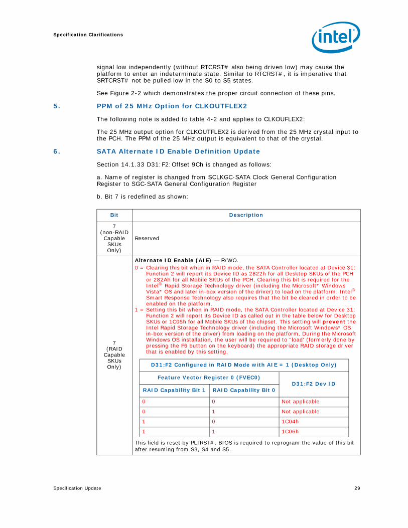
6. SATA Alternate ID Enable Definition Update
Section 14.1.33 D31:F2:Offset 9Ch is changed as follows:
a. Name of register is changed from SCLKGC-SATA Clock General Configuration Register to SGC-SATA General Configuration Register
b. Bit 7 is redefined as shown:
Bit Description
7(non-RAID Capable SKUs Only)
Reserved
7(RAID
Capable SKUs Only)
Alternate ID Enable (AIE) — R/WO. 0 = Clearing this bit when in RAID mode, the SATA Controller located at Device 31:
Function 2 will report its Device ID as 2822h for all Desktop SKUs of the PCH or 282Ah for all Mobile SKUs of the PCH. Clearing this bit is required for the Intel® Rapid Storage Technology driver (including the Microsoft* Windows Vista* OS and later in-box version of the driver) to load on the platform. Intel® Smart Response Technology also requires that the bit be cleared in order to be enabled on the platform.
1 = Setting this bit when in RAID mode, the SATA Controller located at Device 31: Function 2 will report its Device ID as called out in the table below for Desktop SKUs or 1C05h for all Mobile SKUs of the chipset. This setting will prevent the Intel Rapid Storage Technology driver (including the Microsoft Windows* OS in-box version of the driver) from loading on the platform. During the Microsoft Windows OS installation, the user will be required to "load' (formerly done by pressing the F6 button on the keyboard) the appropriate RAID storage driver that is enabled by this setting.
This field is reset by PLTRST#. BIOS is required to reprogram the value of this bit after resuming from S3, S4 and S5.
D31:F2 Configured in RAID Mode with AIE = 1 (Desktop Only)
Feature Vector Register 0 (FVEC0)D31:F2 Dev ID
RAID Capability Bit 1 RAID Capability Bit 0
0 0 Not applicable
0 1 Not applicable
1 0 1C04h
1 1 1C06h
Specification Clarifications
30 Specification Update
c. the following is added to the list of items describing when Intel Rapid Storage Technology is not available in section 5.16.7:
2. The SATA controller is programmed in RAID mode, but the AIE bit (D31:F2:Offset 9Ch bit 7) is set to 1.
d. The SATA D31:F2 Device ID table is updated; see PCH Device and Revision Identification section in this document.
7. SATA Hot Plug Operation
Section 5.16.5 Hot Plug Operation is modified as shown below. Section 5.16.5.1 is removed.
The PCH supports Hot Plug Surprise removal and Insertion Notification. An internal SATA port with a Mechanical Presence Switch can support PARTIAL and SLUMBER with Hot Plug Enabled. Software can take advantage of power savings in the low power states while enabling hot plug operation. Refer to chapter 7 of the AHCI specification for details.
8. GPIO13 Voltage Tolerance
GPIO13 is powered by VccSusHDA well and therefore, the voltage tolerance value varies according to the voltage connected to VccSusHDA. The following clarifications are made:
a. Table 2-24, GPIO13 Tolerance is change from “3.3 V” to “3.3 V or 1.5 V” and the following note is added to table 2-24: “GPIO13 is powered by VccSusHDA (either 3.3 V or 1.5 V). Voltage tolerance on the signal is the same as VccSusHDA.”
b. The following note is added to GPIO13 in table 3-2 as note 16: “GPIO13 is powered by VccSusHDA (either 3.3 V or 1.5 V). Pin tolerance is determined by VccSusHDA voltage.”
c. The following note is added to HDA_DOCK_RST#/GPIO13 in table 3-3 as note 24: “HDA_DOCK_RST#/GPIO13 is powered by VccSusHDA (either 3.3 V or 1.5 V). Pin tolerance is determined by VccSusHDA voltage.”
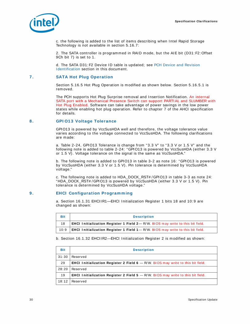
9. EHCI Configuration Programming
a. Section 16.1.31 EHCIIR1—EHCI Initialization Register 1 bits 18 and 10:9 are changed as shown:
b. Section 16.1.32 EHCIIR2—EHCI Initialization Register 2 is modified as shown:
Bit Description
18 EHCI Initialization Register 1 Field 2— R/W. BIOS may write to this bit field.
10:9 EHCI Initialization Register 1 Field 1— R/W. BIOS may write to this bit field.
Bit Description
31:30 Reserved
29 EHCI Initialization Register 2 Field 6 — R/W. BIOS may write to this bit field.
28:20 Reserved
19 EHCI Initialization Register 2 Field 5 — R/W. BIOS may write to this bit field.
18:12 Reserved
Specification Update 31
Specification Clarifications
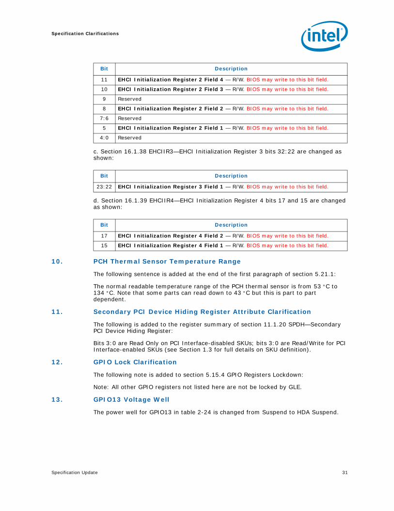
c. Section 16.1.38 EHCIIR3—EHCI Initialization Register 3 bits 32:22 are changed as shown:
d. Section 16.1.39 EHCIIR4—EHCI Initialization Register 4 bits 17 and 15 are changed as shown:
10. PCH Thermal Sensor Temperature Range
The following sentence is added at the end of the first paragraph of section 5.21.1:
The normal readable temperature range of the PCH thermal sensor is from 53 °C to 134 °C. Note that some parts can read down to 43 °C but this is part to part dependent.
The following is added to the register summary of section 11.1.20 SPDH—Secondary PCI Device Hiding Register:
Bits 3:0 are Read Only on PCI Interface-disabled SKUs; bits 3:0 are Read/Write for PCI Interface-enabled SKUs (see Section 1.3 for full details on SKU definition).
12. GPIO Lock Clarification
The following note is added to section 5.15.4 GPIO Registers Lockdown:
Note: All other GPIO registers not listed here are not be locked by GLE.
13. GPIO13 Voltage Well
The power well for GPIO13 in table 2-24 is changed from Suspend to HDA Suspend.
11 EHCI Initialization Register 2 Field 4 — R/W. BIOS may write to this bit field.
10 EHCI Initialization Register 2 Field 3 — R/W. BIOS may write to this bit field.
9 Reserved
8 EHCI Initialization Register 2 Field 2 — R/W. BIOS may write to this bit field.
7:6 Reserved
5 EHCI Initialization Register 2 Field 1 — R/W. BIOS may write to this bit field.
4:0 Reserved
Bit Description
Bit Description
23:22 EHCI Initialization Register 3 Field 1 — R/W. BIOS may write to this bit field.
Bit Description
17 EHCI Initialization Register 4 Field 2 — R/W. BIOS may write to this bit field.
15 EHCI Initialization Register 4 Field 1 — R/W. BIOS may write to this bit field.
Specification Clarifications
32 Specification Update
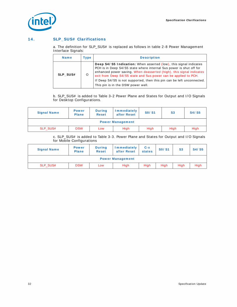
14. SLP_SUS# Clarifications
a. The definition for SLP_SUS# is replaced as follows in table 2-8 Power Management Interface Signals:
b. SLP_SUS# is added to Table 3-2 Power Plane and States for Output and I/O Signals for Desktop Configurations.
c. SLP_SUS# is added to Table 3-3. Power Plane and States for Output and I/O Signals for Mobile Configurations
Name Type Description
SLP_SUS# O
Deep S4/S5 Indication: When asserted (low), this signal indicates PCH is in Deep S4/S5 state where internal Sus power is shut off for enhanced power saving. When deasserted (high), this signal indicates exit from Deep S4/S5 state and Sus power can be applied to PCH.If Deep S4/S5 is not supported, then this pin can be left unconnected.This pin is in the DSW power well.
Signal Name Power Plane
During Reset
Immediately after Reset S0/S1 S3 S4/S5
Power Management
SLP_SUS# DSW Low High High High High
Signal Name Power Plane
During Reset
Immediately after Reset
C-x states S0/S1 S3 S4/S5
Power Management
SLP_SUS# DSW Low High High High High High
Specification Update 33
Specification Clarifications
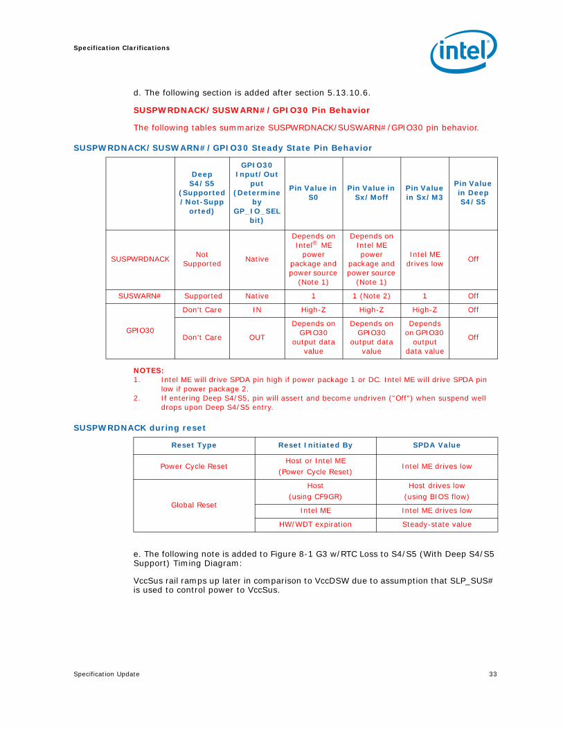
d. The following section is added after section 5.13.10.6.
SUSPWRDNACK/SUSWARN#/GPIO30 Pin Behavior
The following tables summarize SUSPWRDNACK/SUSWARN#/GPIO30 pin behavior.
NOTES:1. Intel ME will drive SPDA pin high if power package 1 or DC. Intel ME will drive SPDA pin
low if power package 2.2. If entering Deep S4/S5, pin will assert and become undriven ("Off") when suspend well
drops upon Deep S4/S5 entry.
e. The following note is added to Figure 8-1 G3 w/RTC Loss to S4/S5 (With Deep S4/S5 Support) Timing Diagram:
VccSus rail ramps up later in comparison to VccDSW due to assumption that SLP_SUS# is used to control power to VccSus.
SUSPWRDNACK/SUSWARN#/GPIO30 Steady State Pin Behavior
Deep S4/S5
(Supported/Not-Supp
orted)
GPIO30 Input/Out
put(Determine
by GP_IO_SEL
bit)
Pin Value in S0
Pin Value in Sx/Moff
Pin Value in Sx/M3
Pin Value in Deep S4/S5
SUSPWRDNACK Not Supported Native
Depends on Intel® ME
power package and power source
(Note 1)
Depends on Intel ME power
package and power source
(Note 1)
Intel ME drives low Off
SUSWARN# Supported Native 1 1 (Note 2) 1 Off
GPIO30
Don't Care IN High-Z High-Z High-Z Off
Don't Care OUT
Depends on GPIO30
output data value
Depends on GPIO30
output data value
Depends on GPIO30
output data value
Off
SUSPWRDNACK during reset
Reset Type Reset Initiated By SPDA Value
Power Cycle ResetHost or Intel ME
(Power Cycle Reset)Intel ME drives low
Global Reset
Host (using CF9GR)
Host drives low (using BIOS flow)
Intel ME Intel ME drives low
HW/WDT expiration Steady-state value
Specification Clarifications
34 Specification Update
15. PME_Turn_Off TLP
The following note is added to section 5.2.2.1 S3/S4/S5 Support:
Note: The PME_Turn_Off TLP messaging flow is also issued during a host reset with and without power cycle. Refer to table 5-38 for a list of host reset sources.
16. GPIO Clarifications
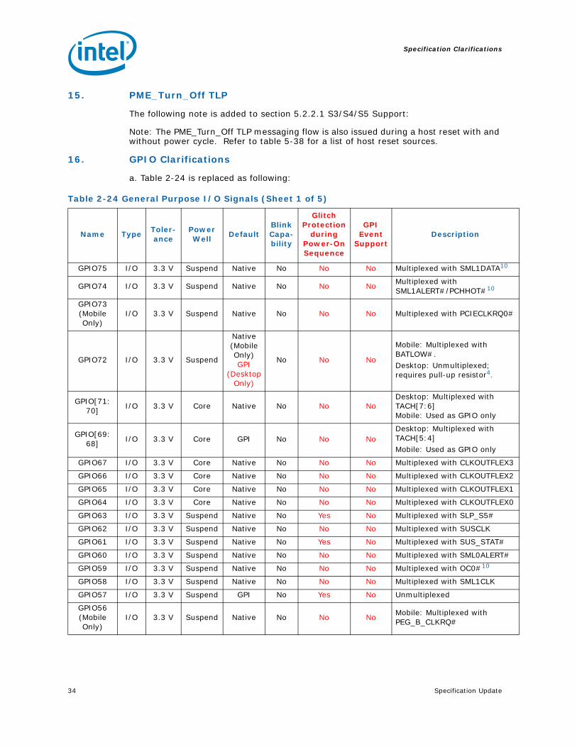
a. Table 2-24 is replaced as following:
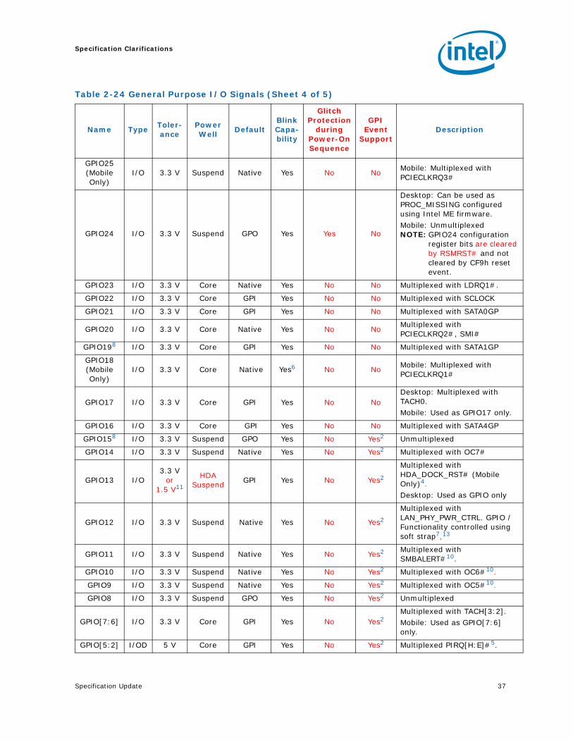
Table 2-24 General Purpose I/O Signals (Sheet 1 of 5)
Name Type Toler-ance
Power Well Default
Blink Capa-bility
Glitch Protection
during Power-On Sequence
GPI Event
SupportDescription
GPIO75 I/O 3.3 V Suspend Native No No No Multiplexed with SML1DATA10
GPIO74 I/O 3.3 V Suspend Native No No No Multiplexed with SML1ALERT#/PCHHOT#10
GPIO73(Mobile Only)
I/O 3.3 V Suspend Native No No No Multiplexed with PCIECLKRQ0#
GPIO72 I/O 3.3 V Suspend
Native (Mobile Only)GPI
(Desktop Only)
No No No
Mobile: Multiplexed with BATLOW#.Desktop: Unmultiplexed; requires pull-up resistor4.
GPIO[71:70] I/O 3.3 V Core Native No No No
Desktop: Multiplexed with TACH[7:6] Mobile: Used as GPIO only
GPIO[69:68] I/O 3.3 V Core GPI No No No
Desktop: Multiplexed with TACH[5:4]Mobile: Used as GPIO only
GPIO67 I/O 3.3 V Core Native No No No Multiplexed with CLKOUTFLEX3
GPIO66 I/O 3.3 V Core Native No No No Multiplexed with CLKOUTFLEX2
GPIO65 I/O 3.3 V Core Native No No No Multiplexed with CLKOUTFLEX1
GPIO64 I/O 3.3 V Core Native No No No Multiplexed with CLKOUTFLEX0
GPIO63 I/O 3.3 V Suspend Native No Yes No Multiplexed with SLP_S5#
GPIO62 I/O 3.3 V Suspend Native No No No Multiplexed with SUSCLK
GPIO61 I/O 3.3 V Suspend Native No Yes No Multiplexed with SUS_STAT#
GPIO60 I/O 3.3 V Suspend Native No No No Multiplexed with SML0ALERT#
GPIO59 I/O 3.3 V Suspend Native No No No Multiplexed with OC0#10
GPIO58 I/O 3.3 V Suspend Native No No No Multiplexed with SML1CLK
GPIO57 I/O 3.3 V Suspend GPI No Yes No Unmultiplexed
GPIO56(Mobile Only)
I/O 3.3 V Suspend Native No No No Mobile: Multiplexed with PEG_B_CLKRQ#
Specification Update 35
Specification Clarifications
GPIO558 I/O 3.3 V Core Native No No NoDesktop: Multiplexed with GNT3# Mobile: Used as GPIO only
GPIO54 I/O 5.0 V Core Native No No NoDesktop: Multiplexed with REQ3#10. Mobile: Used as GPIO only
GPIO538 I/O 3.3 V Core Native No No NoDesktop: Multiplexed with GNT2#Mobile: Used as GPIO only
GPIO52 I/O 5.0 V Core Native No No NoDesktop: Multiplexed with REQ2#10.Mobile: Used as GPIO only
GPIO518 I/O 3.3 V Core Native No No NoDesktop: Multiplexed with GNT1#Mobile: Used as GPIO only
GPIO50 I/O 5.0 V Core Native No No NoDesktop: Multiplexed with REQ1#10.Mobile: Used as GPIO only
GPIO49 I/O 3.3 V Core GPI No No No Multiplexed with SATA5GP and TEMP_ALERT#
GPIO48 I/O 3.3 V Core GPI No No No Multiplexed with SDATAOUT1.
GPIO47(Mobile Only)
I/O 3.3 V Suspend Native No No No Multiplexed with PEG_A_CLKRQ#
GPIO46 I/O 3.3 V Suspend Native No No No Multiplexed with PCIECLKRQ7#
GPIO45 I/O 3.3 V Suspend Native No No No Multiplexed with PCIECLKRQ6#
GPIO44 I/O 3.3 V Suspend Native No No No Multiplexed with PCIECLKRQ5#
GPIO[43:40] I/O 3.3 V Suspend Native No No No Multiplexed with OC[4:1]#10.
GPIO39 I/O 3.3 V Core GPI No No No Multiplexed with SDATAOUT0.
GPIO38 I/O 3.3 V Core GPI No No No Multiplexed with SLOAD.
GPIO378 I/O 3.3 V Core GPI No No No Multiplexed with SATA3GP.
GPIO368 I/O 3.3 V Core GPI No No No Multiplexed with SATA2GP.
GPIO35 I/O 3.3 V Core GPO No No No Multiplexed with NMI#.
GPIO34 I/O 3.3 V Core GPI No No No Multiplexed with STP_PCI#
GPIO33 I/O 3.3 V Core GPO No No No
Mobile: Multiplexed with HDA_DOCK_EN# (Mobile Only)4.Desktop: Used as GPIO only
GPIO32(not
available in Mobile)
I/O 3.3 V Core
GPO, Native (Mobile only)
No No No
Unmultiplexed (Desktop Only)Mobile Only: Used as CLKRUN#, unavailable as GPIO4.
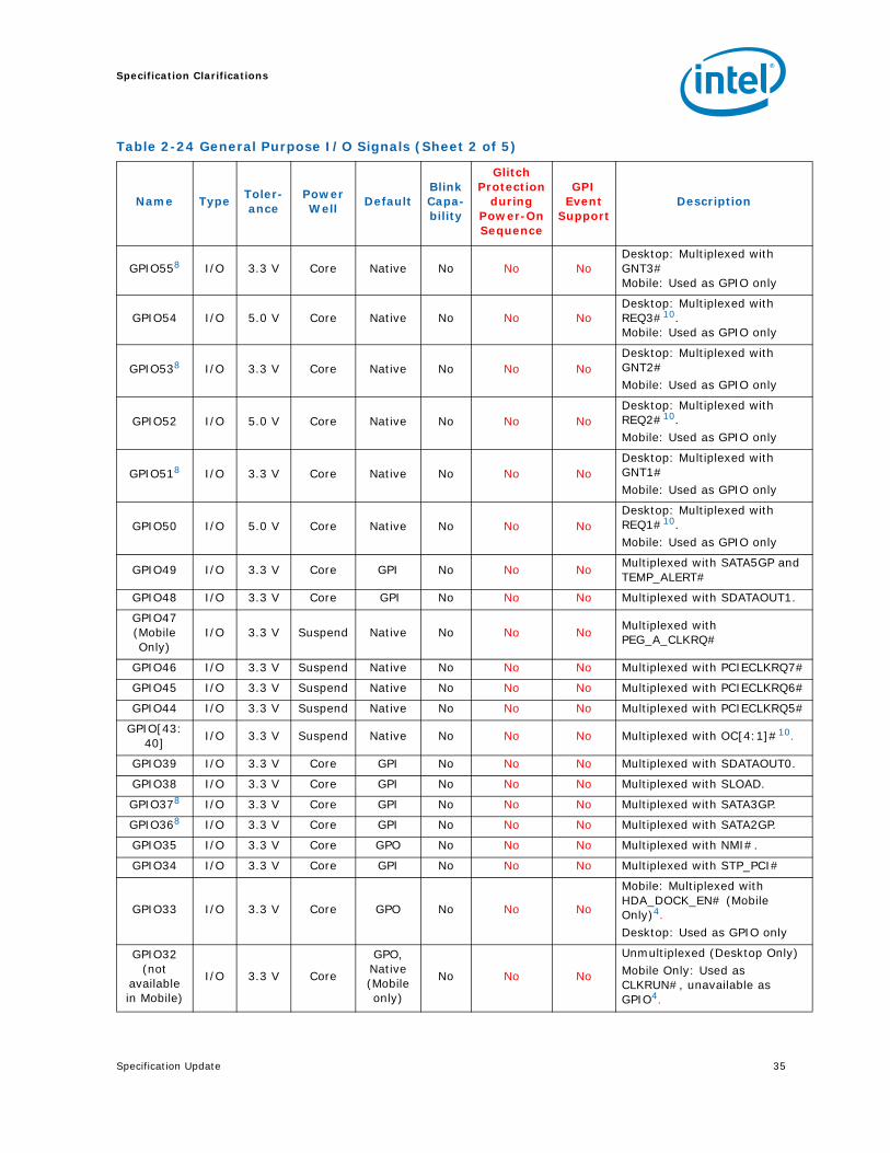
Table 2-24 General Purpose I/O Signals (Sheet 2 of 5)
Name Type Toler-ance
Power Well Default
Blink Capa-bility
Glitch Protection
during Power-On Sequence
GPI Event
SupportDescription
Specification Clarifications
36 Specification Update
GPIO31 I/O 3.3 V DSW12 GPI Yes Yes No
Multiplexed with ACPRESENT.Mobile: This GPIO pin is permanently appropriated by the Intel ME for ACPRESENT function.Desktop: This pin is only GPIO31.NOTES:1. Toggling this pin at a
frequency higher than 10 Hz is not supported.
2. GPIO_USE_SEL[31] is internally hardwired to a lb, which means GPIO mode is permanently selected and cannot be changed.
GPIO30 I/O 3.3 V Suspend Native Yes Yes No
Multiplexed with SUSPWRDNACK, SUSWARN#Desktop: Can be configured as SUSWARN# or GPIO30 only. Cannot be used as SUSPWRDNACK.Mobile: Used as SUSPWRDNACK, SUSWARN#, or GPIO30
GPIO29 I/O 3.3 V Suspend Native Yes Yes No
Multiplexed with SLP_LAN# Pin usage as GPIO is determined by SLP_LAN#/GPIO Select Soft-strap9. Soft-strap value is not preserved for this signal in the Sx/Moff state and the pin will return to its native functionality (SLP_LAN#)
GPIO288 I/O 3.3 V Suspend GPO Yes No No Unmultiplexed
GPIO27 I/O 3.3 V DSW12 GPI Yes No No
Unmultiplexed. Can be configured as wake input to allow wakes from Deep S4/S5. This GPIO has no GPIO functionality in the Deep S4/S5 states other than wake from Deep S4/S5 if this option has been configured.
GPIO26(Mobile Only)
I/O 3.3 V Suspend Native Yes No No Mobile: Multiplexed with PCIECLKRQ4#
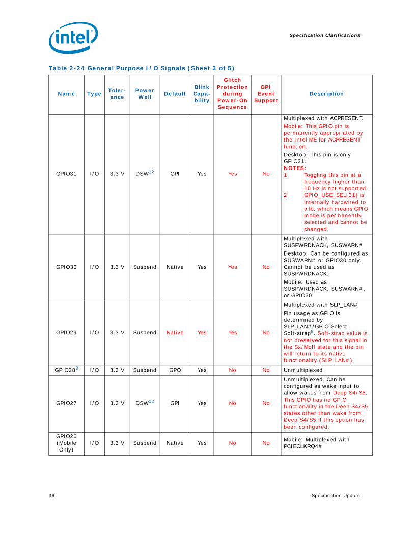
Table 2-24 General Purpose I/O Signals (Sheet 3 of 5)
Name Type Toler-ance
Power Well Default
Blink Capa-bility
Glitch Protection
during Power-On Sequence
GPI Event
SupportDescription
Specification Update 37
Specification Clarifications
GPIO25 (Mobile Only)
I/O 3.3 V Suspend Native Yes No No Mobile: Multiplexed with PCIECLKRQ3#
GPIO24 I/O 3.3 V Suspend GPO Yes Yes No
Desktop: Can be used as PROC_MISSING configured using Intel ME firmware.Mobile: UnmultiplexedNOTE: GPIO24 configuration
register bits are cleared by RSMRST# and not cleared by CF9h reset event.
GPIO23 I/O 3.3 V Core Native Yes No No Multiplexed with LDRQ1#.
GPIO22 I/O 3.3 V Core GPI Yes No No Multiplexed with SCLOCK
GPIO21 I/O 3.3 V Core GPI Yes No No Multiplexed with SATA0GP
GPIO20 I/O 3.3 V Core Native Yes No No Multiplexed with PCIECLKRQ2#, SMI#
GPIO198 I/O 3.3 V Core GPI Yes No No Multiplexed with SATA1GP
GPIO18 (Mobile Only)
I/O 3.3 V Core Native Yes6 No No Mobile: Multiplexed with PCIECLKRQ1#
GPIO17 I/O 3.3 V Core GPI Yes No NoDesktop: Multiplexed with TACH0.Mobile: Used as GPIO17 only.
GPIO16 I/O 3.3 V Core GPI Yes No No Multiplexed with SATA4GP
GPIO158 I/O 3.3 V Suspend GPO Yes No Yes2 Unmultiplexed
GPIO14 I/O 3.3 V Suspend Native Yes No Yes2 Multiplexed with OC7#
GPIO13 I/O3.3 V
or 1.5 V11
HDA Suspend GPI Yes No Yes2
Multiplexed with HDA_DOCK_RST# (Mobile Only)4.Desktop: Used as GPIO only
GPIO12 I/O 3.3 V Suspend Native Yes No Yes2
Multiplexed with LAN_PHY_PWR_CTRL. GPIO / Functionality controlled using soft strap7,13
GPIO11 I/O 3.3 V Suspend Native Yes No Yes2 Multiplexed with SMBALERT#10.
GPIO10 I/O 3.3 V Suspend Native Yes No Yes2 Multiplexed with OC6#10.
GPIO9 I/O 3.3 V Suspend Native Yes No Yes2 Multiplexed with OC5#10.
GPIO8 I/O 3.3 V Suspend GPO Yes No Yes2 Unmultiplexed
GPIO[7:6] I/O 3.3 V Core GPI Yes No Yes2Multiplexed with TACH[3:2].Mobile: Used as GPIO[7:6] only.
GPIO[5:2] I/OD 5 V Core GPI Yes No Yes2 Multiplexed PIRQ[H:E]#5.
Table 2-24 General Purpose I/O Signals (Sheet 4 of 5)
Name Type Toler-ance
Power Well Default
Blink Capa-bility
Glitch Protection
during Power-On Sequence
GPI Event
SupportDescription
Specification Clarifications
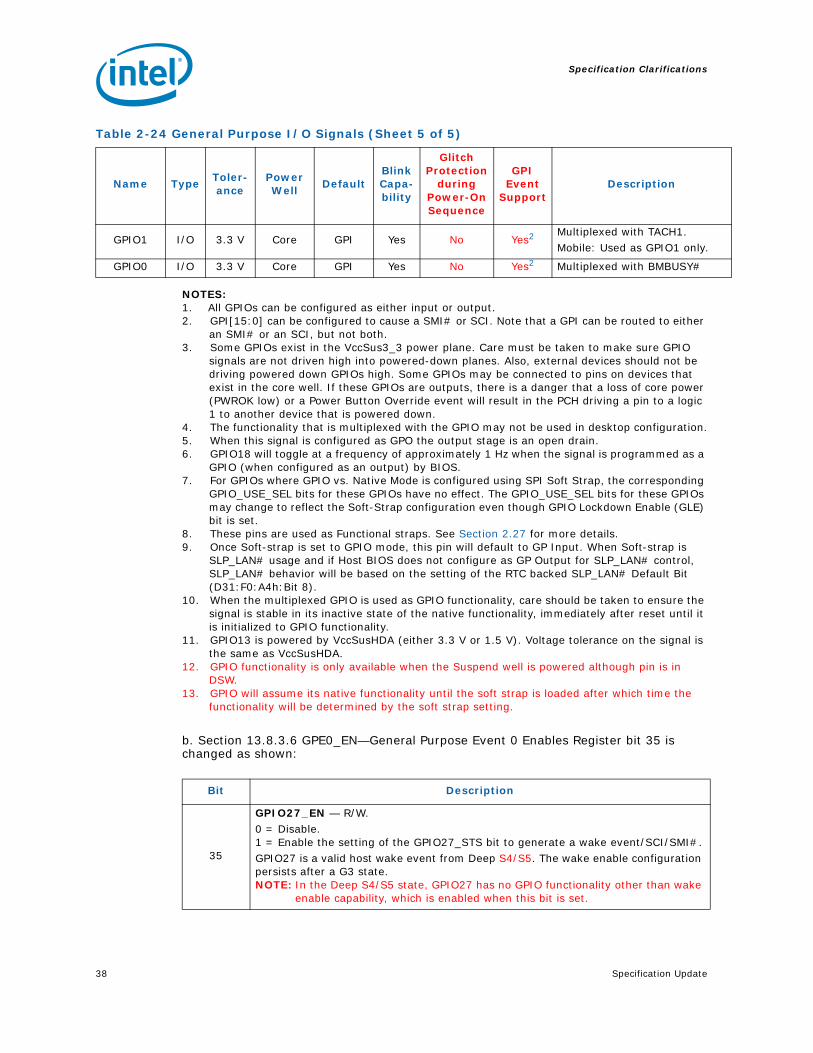
38 Specification Update
NOTES:1. All GPIOs can be configured as either input or output.2. GPI[15:0] can be configured to cause a SMI# or SCI. Note that a GPI can be routed to either
an SMI# or an SCI, but not both.3. Some GPIOs exist in the VccSus3_3 power plane. Care must be taken to make sure GPIO
signals are not driven high into powered-down planes. Also, external devices should not be driving powered down GPIOs high. Some GPIOs may be connected to pins on devices that exist in the core well. If these GPIOs are outputs, there is a danger that a loss of core power (PWROK low) or a Power Button Override event will result in the PCH driving a pin to a logic 1 to another device that is powered down.
4. The functionality that is multiplexed with the GPIO may not be used in desktop configuration.5. When this signal is configured as GPO the output stage is an open drain.6. GPIO18 will toggle at a frequency of approximately 1 Hz when the signal is programmed as a
GPIO (when configured as an output) by BIOS.7. For GPIOs where GPIO vs. Native Mode is configured using SPI Soft Strap, the corresponding
GPIO_USE_SEL bits for these GPIOs have no effect. The GPIO_USE_SEL bits for these GPIOs may change to reflect the Soft-Strap configuration even though GPIO Lockdown Enable (GLE) bit is set.
8. These pins are used as Functional straps. See Section 2.27 for more details.9. Once Soft-strap is set to GPIO mode, this pin will default to GP Input. When Soft-strap is
SLP_LAN# usage and if Host BIOS does not configure as GP Output for SLP_LAN# control, SLP_LAN# behavior will be based on the setting of the RTC backed SLP_LAN# Default Bit (D31:F0:A4h:Bit 8).
10. When the multiplexed GPIO is used as GPIO functionality, care should be taken to ensure the signal is stable in its inactive state of the native functionality, immediately after reset until it is initialized to GPIO functionality.
11. GPIO13 is powered by VccSusHDA (either 3.3 V or 1.5 V). Voltage tolerance on the signal is the same as VccSusHDA.
12. GPIO functionality is only available when the Suspend well is powered although pin is in DSW.
13. GPIO will assume its native functionality until the soft strap is loaded after which time the functionality will be determined by the soft strap setting.
b. Section 13.8.3.6 GPE0_EN—General Purpose Event 0 Enables Register bit 35 is changed as shown:
GPIO1 I/O 3.3 V Core GPI Yes No Yes2 Multiplexed with TACH1.Mobile: Used as GPIO1 only.
GPIO0 I/O 3.3 V Core GPI Yes No Yes2 Multiplexed with BMBUSY#
Table 2-24 General Purpose I/O Signals (Sheet 5 of 5)
Name Type Toler-ance
Power Well Default
Blink Capa-bility
Glitch Protection
during Power-On Sequence
GPI Event
SupportDescription
Bit Description
35
GPIO27_EN — R/W.0 = Disable.1 = Enable the setting of the GPIO27_STS bit to generate a wake event/SCI/SMI#.GPIO27 is a valid host wake event from Deep S4/S5. The wake enable configuration persists after a G3 state.NOTE: In the Deep S4/S5 state, GPIO27 has no GPIO functionality other than wake
enable capability, which is enabled when this bit is set.
Specification Update 39
Specification Clarifications
17. Power Button Override and Deep S4/S5
a. The following note is added to the PWRBTN# Description in table 2-8 Power Management Interface Signals:
Note: Upon entry to S5 due to a power button override, if Deep S4/S5 is enabled and conditions are met per section 5.13.7.6, the system will transition to Deep S4/S5.
b. The following is added as note 5 to table 5-23 State Transition Rules for the PCH and applies to all Power Button Override statements in the table:
Note: Upon entry to S5 due to a power button override, if Deep S4/S5 is enabled and conditions are met per section 5.13.7.6, the system will transition to Deep S4/S5.
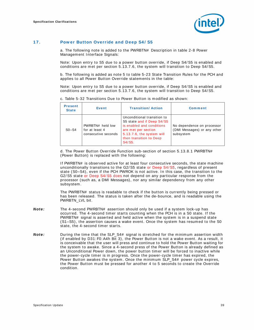
c. Table 5-32 Transitions Due to Power Button is modified as shown:
d. The Power Button Override Function sub-section of section 5.13.8.1 PWRBTN# (Power Button) is replaced with the following:
If PWRBTN# is observed active for at least four consecutive seconds, the state machine unconditionally transitions to the G2/S5 state or Deep S4/S5, regardless of present state (S0–S4), even if the PCH PWROK is not active. In this case, the transition to the G2/S5 state or Deep S4/S5 does not depend on any particular response from the processor (such as, a DMI Messages), nor any similar dependency from any other subsystem.
The PWRBTN# status is readable to check if the button is currently being pressed or has been released. The status is taken after the de-bounce, and is readable using the PWRBTN_LVL bit.
Note: The 4-second PWRBTN# assertion should only be used if a system lock-up has occurred. The 4-second timer starts counting when the PCH is in a S0 state. If the PWRBTN# signal is asserted and held active when the system is in a suspend state (S1–S5), the assertion causes a wake event. Once the system has resumed to the S0 state, the 4-second timer starts.
Note: During the time that the SLP_S4# signal is stretched for the minimum assertion width (if enabled by D31:F0:A4h Bit 3), the Power Button is not a wake event. As a result, it is conceivable that the user will press and continue to hold the Power Button waiting for the system to awake. Since a 4-second press of the Power Button is already defined as an Unconditional Power down, the power button timer will be forced to inactive while the power-cycle timer is in progress. Once the power-cycle timer has expired, the Power Button awakes the system. Once the minimum SLP_S4# power cycle expires, the Power Button must be pressed for another 4 to 5 seconds to create the Override condition.
Present State Event Transition/Action Comment
S0–S4PWRBTN# held low for at least 4 consecutive seconds
Unconditional transition to S5 state and if Deep S4/S5 is enabled and conditions are met per section 5.13.7.6, the system will then transition to Deep S4/S5.
No dependence on processor (DMI Messages) or any other subsystem
Specification Clarifications
40 Specification Update
e. Note 6 is added to the “Straight to S5 (Host Stays there) column in Table 5-38 Causes of Host and Global Resets:
6. Upon entry to S5, if Deep S4/S5 is enabled and conditions are met per section 5.13.7.6, the system will transition to Deep S4/S5.
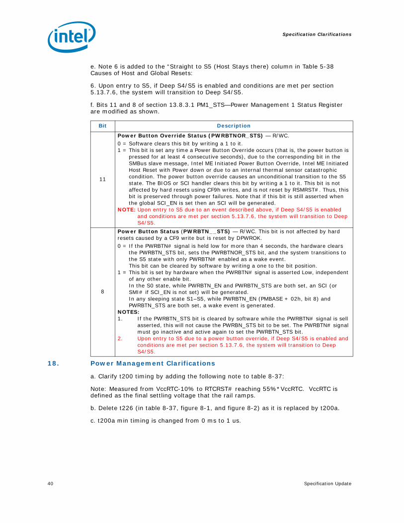
f. Bits 11 and 8 of section 13.8.3.1 PM1_STS—Power Management 1 Status Register are modified as shown.
18. Power Management Clarifications
a. Clarify t200 timing by adding the following note to table 8-37:
Note: Measured from VccRTC-10% to RTCRST# reaching 55%*VccRTC. VccRTC is defined as the final settling voltage that the rail ramps.
b. Delete t226 (in table 8-37, figure 8-1, and figure 8-2) as it is replaced by t200a.
c. t200a min timing is changed from 0 ms to 1 us.
Bit Description
11
Power Button Override Status (PWRBTNOR_STS) — R/WC.0 = Software clears this bit by writing a 1 to it.1 = This bit is set any time a Power Button Override occurs (that is, the power button is
pressed for at least 4 consecutive seconds), due to the corresponding bit in the SMBus slave message, Intel ME Initiated Power Button Override, Intel ME Initiated Host Reset with Power down or due to an internal thermal sensor catastrophic condition. The power button override causes an unconditional transition to the S5 state. The BIOS or SCI handler clears this bit by writing a 1 to it. This bit is not affected by hard resets using CF9h writes, and is not reset by RSMRST#. Thus, this bit is preserved through power failures. Note that if this bit is still asserted when the global SCI_EN is set then an SCI will be generated.
NOTE: Upon entry to S5 due to an event described above, if Deep S4/S5 is enabled and conditions are met per section 5.13.7.6, the system will transition to Deep S4/S5.
8
Power Button Status (PWRBTN__STS) — R/WC. This bit is not affected by hard resets caused by a CF9 write but is reset by DPWROK.0 = If the PWRBTN# signal is held low for more than 4 seconds, the hardware clears
the PWRBTN_STS bit, sets the PWRBTNOR_STS bit, and the system transitions to the S5 state with only PWRBTN# enabled as a wake event. This bit can be cleared by software by writing a one to the bit position.
1 = This bit is set by hardware when the PWRBTN# signal is asserted Low, independent of any other enable bit. In the S0 state, while PWRBTN_EN and PWRBTN_STS are both set, an SCI (or SMI# if SCI_EN is not set) will be generated. In any sleeping state S1–S5, while PWRBTN_EN (PMBASE + 02h, bit 8) and PWRBTN_STS are both set, a wake event is generated.
NOTES:1. If the PWRBTN_STS bit is cleared by software while the PWRBTN# signal is sell
asserted, this will not cause the PWRBN_STS bit to be set. The PWRBTN# signal must go inactive and active again to set the PWRBTN_STS bit.
2. Upon entry to S5 due to a power button override, if Deep S4/S5 is enabled and conditions are met per section 5.13.7.6, the system will transition to Deep S4/S5.
Specification Update 41
Specification Clarifications
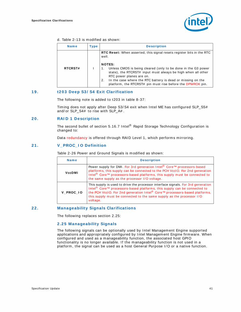
d. Table 2-13 is modified as shown:
19. t203 Deep S3/S4 Exit Clarification
The following note is added to t203 in table 8-37:
Timing does not apply after Deep S3/S4 exit when Intel ME has configured SLP_S5# and/or SLP_S4# to rise with SLP_A#.
20. RAID 1 Description
The second bullet of section 5.16.7 Intel® Rapid Storage Technology Configuration is changed to:
Data redundancy is offered through RAID Level 1, which performs mirroring.
21. V_PROC_IO Definition
Table 2-26 Power and Ground Signals is modified as shown:
22. Manageability Signals Clarifications
The following replaces section 2.25:
2.25 Manageability SignalsThe following signals can be optionally used by Intel Management Engine supported applications and appropriately configured by Intel Management Engine firmware. When configured and used as a manageability function, the associated host GPIO functionality is no longer available. If the manageability function is not used in a platform, the signal can be used as a host General Purpose I/O or a native function.
Name Type Description
RTCRST# I
RTC Reset: When asserted, this signal resets register bits in the RTC well.
NOTES:1. Unless CMOS is being cleared (only to be done in the G3 power
state), the RTCRST# input must always be high when all other RTC power planes are on.
2. In the case where the RTC battery is dead or missing on the platform, the RTCRST# pin must rise before the DPWROK pin.
Name Description
VccDMI
Power supply for DMI. For 3rd generation Intel® Core™ processors-based platforms, this supply can be connected to the PCH VccIO. For 2nd generation Intel® Core™ processors-based platforms, this supply must be connected to the same supply as the processor I/O voltage.
V_PROC_IO
This supply is used to drive the processor interface signals. For 3rd generation Intel® Core™ processors-based platforms, this supply can be connected to the PCH VccIO. For 2nd generation Intel® Core™ processors-based platforms, this supply must be connected to the same supply as the processor I/O voltage.
Specification Clarifications
42 Specification Update
NOTES:1. Manageability functionality can be assigned to at most one pin and is configured through
Intel ME FW.2. See GPIO table for power well each Pin Name is associated with in Section 2-24.
NOTES:1. Manageability functionality can be assigned to at most one pin and is configured through
Intel ME FW.2. See GPIO table for power well each Pin Name is associated with in Section 2-24.
Table 2-25 Desktop/Mobile Manageability Signals
Functionality Name Functionality Description Pin Name(s)1
SUSWARN# or SUSPWRDNACK (Mobile Only)
Used by Intel® ME as either SUSWARN# in Deep S4/S5 state supported platforms or as SUSPWRDNACK in non Deep S4/S5 state supported platforms.
SUSWARN# /SUSPWRDNACK#/
GPIO30
AC Present(Mobile Only)
Input signal from the Embedded Controller (EC) on Mobile systems to indicate AC power source or the system battery. Active High indicates AC power.
ACPRESENT / GPIO31
Temperature Alert
Used as an alert (active low) to indicate to the external controller (such as EC or SIO) that temperatures are out of range for the PCH or Graphics/Memory Controller or the processor core.
SATA5GP / GPIO49 / TEMP_ALERT#
Processor Missing
(Desktop Only)
Used to indicate Processor Missing to the Intel Management Engine.
GPIO24 / PROC_MISSING
Table 2-26 Server Manageability Signals
Functionality Name Functionality Description MGPIO Name(s)1
SMBALERT# signal from PSU
to PCH
Indicates the PSU may cause system shutdown due to a momentary loss of AC input voltage or an over temperature condition.
MGPIO2
Intel ME FW Recovery Mode
Strap
Input to PCH to force Intel ME to stay in recovery boot loader.
Table 2-27 Server MGPIO Signal to Pin Name Conversion Table (Sheet 1 of 2)
MGPIO Ballout Pin Name
MGPIO0 GPIO24/PROC_MISSING
MGPIO1 SUSWARN#/GPIO30
MGPIO2 GPIO31
MGPIO3 SLP_LAN#/GPIO29
MGPIO4 SML0ALERT#/GPIO60
MGPIO5 GPIO57
Specification Update 43
Specification Clarifications
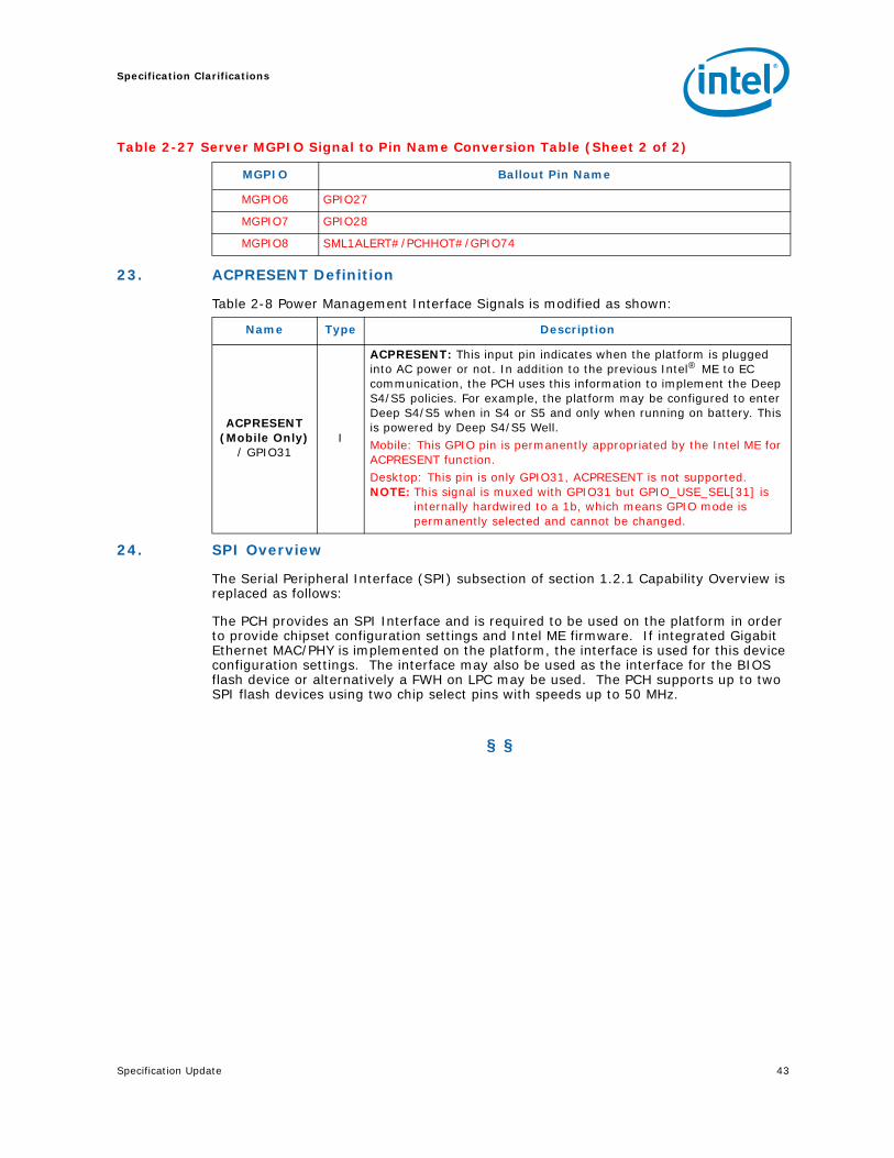
23. ACPRESENT Definition
Table 2-8 Power Management Interface Signals is modified as shown:
24. SPI Overview
The Serial Peripheral Interface (SPI) subsection of section 1.2.1 Capability Overview is replaced as follows:
The PCH provides an SPI Interface and is required to be used on the platform in order to provide chipset configuration settings and Intel ME firmware. If integrated Gigabit Ethernet MAC/PHY is implemented on the platform, the interface is used for this device configuration settings. The interface may also be used as the interface for the BIOS flash device or alternatively a FWH on LPC may be used. The PCH supports up to two SPI flash devices using two chip select pins with speeds up to 50 MHz.
§ §
MGPIO6 GPIO27
MGPIO7 GPIO28
MGPIO8 SML1ALERT#/PCHHOT#/GPIO74
Table 2-27 Server MGPIO Signal to Pin Name Conversion Table (Sheet 2 of 2)
MGPIO Ballout Pin Name
Name Type Description
ACPRESENT (Mobile Only)
/ GPIO31I
ACPRESENT: This input pin indicates when the platform is plugged into AC power or not. In addition to the previous Intel® ME to EC communication, the PCH uses this information to implement the Deep S4/S5 policies. For example, the platform may be configured to enter Deep S4/S5 when in S4 or S5 and only when running on battery. This is powered by Deep S4/S5 Well.Mobile: This GPIO pin is permanently appropriated by the Intel ME for ACPRESENT function.Desktop: This pin is only GPIO31, ACPRESENT is not supported.NOTE: This signal is muxed with GPIO31 but GPIO_USE_SEL[31] is
internally hardwired to a 1b, which means GPIO mode is permanently selected and cannot be changed.
Documentation Changes
44 Specification Update
Documentation Changes
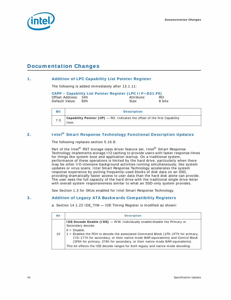
1. Addition of LPC Capability List Pointer Register
Part of the Intel® RST storage class driver feature set, Intel® Smart Response Technology implements storage I/O caching to provide users with faster response times for things like system boot and application startup. On a traditional system, performance of these operations is limited by the hard drive, particularly when there may be other I/O intensive background activities running simultaneously, like system updates or virus scans. Intel Smart Response Technology accelerates the system response experience by putting frequently-used blocks of disk data on an SSD, providing dramatically faster access to user data than the hard disk alone can provide. The user sees the full capacity of the hard drive with the traditional single drive letter with overall system responsiveness similar to what an SSD-only system provides.
See Section 1.3 for SKUs enabled for Intel Smart Response Technology.
3. Addition of Legacy ATA Backwards Compatibility Registers
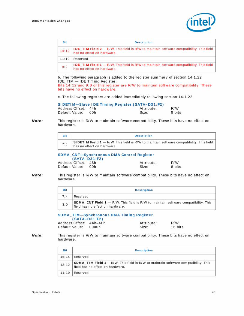
a. Section 14.1.22 IDE_TIM — IDE Timing Register is modified as shown:
Bit Description
7:0Capability Pointer (CP) — RO. Indicates the offset of the first CapabilityItem.
Bit Description
15
IDE Decode Enable (IDE) — R/W. Individually enable/disable the Primary or Secondary decode. 0 = Disable.1 = Enables the PCH to decode the associated Command Block (1F0–1F7h for primary,
170–177h for secondary, or their native mode BAR equivalents) and Control Block (3F6h for primary, 376h for secondary, or their native mode BAR equivalents).
This bit effects the IDE decode ranges for both legacy and native-mode decoding.
Specification Update 45
Documentation Changes
b. The following paragraph is added to the register summary of section 14.1.22 IDE_TIM — IDE Timing Register:Bits 14:12 and 9:0 of this register are R/W to maintain software compatibility. These bits have no effect on hardware.
c. The following registers are added immediately following section 14.1.22:
Note: This register is R/W to maintain software compatibility. These bits have no effect on hardware.
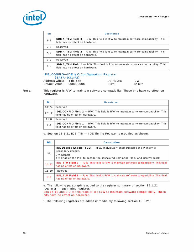
d. Section 15.1.21 IDE_TIM — IDE Timing Register is modified as shown:
e. The following paragraph is added to the register summary of section 15.1.21 IDE_TIM — IDE Timing Register:Bits 14:12 and 9:0 of this register are R/W to maintain software compatibility. These bits have no effect on hardware.
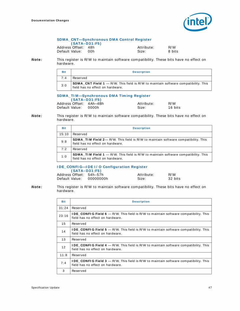
f. The following registers are added immediately following section 15.1.21:
9:8 SDMA_TIM Field 3— R/W. This field is R/W to maintain software compatibility. This field has no effect on hardware.
7:6 Reserved
5:4 SDMA_TIM Field 2— R/W. This field is R/W to maintain software compatibility. This field has no effect on hardware.
3:2 Reserved
1:0 SDMA_TIM Field 1 — R/W. This field is R/W to maintain software compatibility. This field has no effect on hardware.
Bit Description
Bit Description
31:24 Reserved
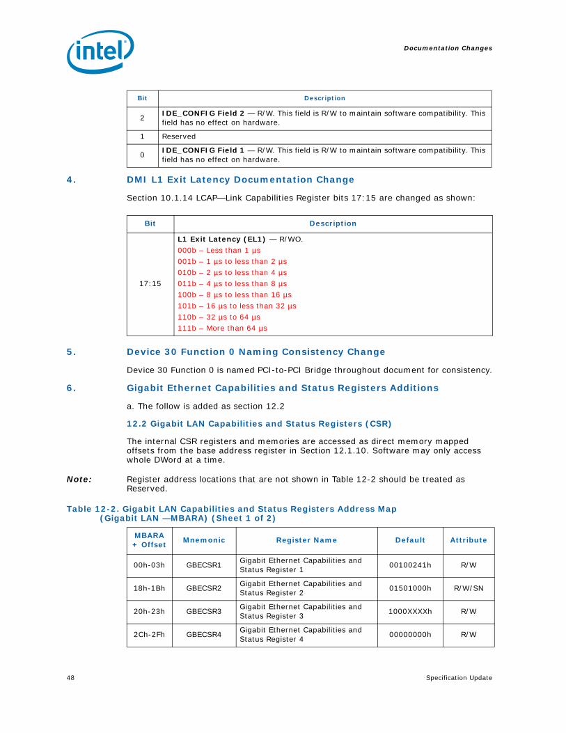
23:12 IDE_CONFIG Field 2 — R/W. This field is R/W to maintain software compatibility. This field has no effect on hardware.
11:8 Reserved
7:0 IDE_CONFIG Field 1 — R/W. This field is R/W to maintain software compatibility. This field has no effect on hardware.
Bit Description
15
IDE Decode Enable (IDE) — R/W. Individually enable/disable the Primary or Secondary decode. 0 = Disable.1 = Enables the PCH to decode the associated Command Block and Control Block.
14:12 IDE_TIM Field 2 — R/W. This field is R/W to maintain software compatibility. This field has no effect on hardware.
11:10 Reserved
9:0 IDE_TIM Field 1 — R/W. This field is R/W to maintain software compatibility. This field has no effect on hardware.
Specification Update 47
Documentation Changes
SDMA_CNT—Synchronous DMA Control Register (SATA–D31:F5)
Note: This register is R/W to maintain software compatibility. These bits have no effect on hardware.
Bit Description
7:4 Reserved
3:0 SDMA_CNT Field 1 — R/W. This field is R/W to maintain software compatibility. This field has no effect on hardware.
Bit Description
15:10 Reserved
9:8 SDMA_TIM Field 2— R/W. This field is R/W to maintain software compatibility. This field has no effect on hardware.
7:2 Reserved
1:0 SDMA_TIM Field 1 — R/W. This field is R/W to maintain software compatibility. This field has no effect on hardware.
Bit Description
31:24 Reserved
23:16 IDE_CONFIG Field 6 — R/W. This field is R/W to maintain software compatibility. This field has no effect on hardware.
15 Reserved
14 IDE_CONFIG Field 5 — R/W. This field is R/W to maintain software compatibility. This field has no effect on hardware.
13 Reserved
12 IDE_CONFIG Field 4 — R/W. This field is R/W to maintain software compatibility. This field has no effect on hardware.
11:8 Reserved
7:4 IDE_CONFIG Field 3 — R/W. This field is R/W to maintain software compatibility. This field has no effect on hardware.
3 Reserved
Documentation Changes
48 Specification Update
4. DMI L1 Exit Latency Documentation Change
Section 10.1.14 LCAP—Link Capabilities Register bits 17:15 are changed as shown:
5. Device 30 Function 0 Naming Consistency Change
Device 30 Function 0 is named PCI-to-PCI Bridge throughout document for consistency.
6. Gigabit Ethernet Capabilities and Status Registers Additions
a. The follow is added as section 12.2
12.2 Gigabit LAN Capabilities and Status Registers (CSR)
The internal CSR registers and memories are accessed as direct memory mapped offsets from the base address register in Section 12.1.10. Software may only access whole DWord at a time.
Note: Register address locations that are not shown in Table 12-2 should be treated as Reserved.
2 IDE_CONFIG Field 2 — R/W. This field is R/W to maintain software compatibility. This field has no effect on hardware.
1 Reserved
0 IDE_CONFIG Field 1 — R/W. This field is R/W to maintain software compatibility. This field has no effect on hardware.
Bit Description
Bit Description
17:15
L1 Exit Latency (EL1) — R/WO.000b – Less than 1 µs001b – 1 µs to less than 2 µs010b – 2 µs to less than 4 µs011b – 4 µs to less than 8 µs100b – 8 µs to less than 16 µs101b – 16 µs to less than 32 µs110b – 32 µs to 64 µs111b – More than 64 µs
Table 12-2. Gigabit LAN Capabilities and Status Registers Address Map (Gigabit LAN —MBARA) (Sheet 1 of 2)
MBARA + Offset Mnemonic Register Name Default Attribute
00h-03h GBECSR1 Gigabit Ethernet Capabilities and Status Register 1 00100241h R/W
18h-1Bh GBECSR2 Gigabit Ethernet Capabilities and Status Register 2 01501000h R/W/SN
20h-23h GBECSR3 Gigabit Ethernet Capabilities and Status Register 3 1000XXXXh R/W
2Ch-2Fh GBECSR4 Gigabit Ethernet Capabilities and Status Register 4 00000000h R/W
Specification Update 49
Documentation Changes
12.2.1 GBECSR1—Gigabit Ethernet Capabilities and Status Register 1Address Offset: MBARA + 00h Attribute: R/WDefault Value: 00100241h Size: 32 bit
12.2.2 GBECSR2—Gigabit Ethernet Capabilities and Status Register 2Address Offset: MBARA + 18h Attribute: R/W/SNDefault Value: 01501000h Size: 32 bit
F00h-F03h GBECSR5 Gigabit Ethernet Capabilities and
Status Register 5 00010008h R/W
F10h-F13h GBECSR6 Gigabit Ethernet Capabilities and
Status Register 6 0004000Ch R/W/SN
5400h-5403h GBECSR7 Gigabit Ethernet Capabilities and
Status Register 7 XXXXXXXXh R/W
5404h-5407h GBECSR8 Gigabit Ethernet Capabilities and
Status Register 8 XXXXXXXXh R/W
5800h-5803h GBECSR9 Gigabit Ethernet Capabilities and
Status Register 9 00000008h R/W/SN
Table 12-2. Gigabit LAN Capabilities and Status Registers Address Map (Gigabit LAN —MBARA) (Sheet 2 of 2)
MBARA + Offset Mnemonic Register Name Default Attribute
Bit Description
31:25 Reserved
24PHY Power Down (PHYPDN) — R/W.When cleared (0b), the PHY power down setting is controlled by the internal logic of PCH.
23:0 Reserved
Bit Description
31:21 Reserved
20PHY Power Down Enable (PHYPDEN) — R/W/SN.When set, this bit enables the PHY to enter a low-power state when the LAN controller is at the DMoff/D3 or with no WOL.
19:0 Reserved
Documentation Changes
50 Specification Update
12.2.3 GBECSR3—Gigabit Ethernet Capabilities and Status Register 3Address Offset: MBARA + 20h Attribute: R/WDefault Value: 1000XXXXh Size: 32 bit
12.2.4 GBECSR4—Gigabit Ethernet Capabilities and Status Register 4Address Offset: MBARA + 2Ch Attribute: R/WDefault Value: 00000000h Size: 32 bits
12.2.5 GBECSR5—Gigabit Ethernet Capabilities and Status Register 5Address Offset: MBARA + F00h Attribute: R/WDefault Value: 00010008h Size: 32 bits
Bit Description
31:29 Reserved
28Ready Bit (RB) — R/W. Set to 1 by the Gigabit Ethernet Controller at the end of the MDI transaction. This bit should be reset to 0 by software at the same time the command is written.
27:26
MDI Type — R/W.01 = MDI Write10 = MDI ReadAll other values are reserved.
25:21 LAN Connected Device Address (PHYADD) — R/W.
20:16 LAN Connected Device Register Address (PHYREGADD) — R/W.
15:0 DATA — R/W.
Bit Description
31WOL Indication Valid (WIV) — R/W.Set to 1 by BIOS to indicate that the WOL indication setting in bit 30 of this register is valid.
30WOL Enable Setting by BIOS (WESB) — R/W. 1 = WOL Enabled in BIOS.0 = WOL Disabled in BIOS.
29:0 Reserved
Bit Description
31:6 Reserved
5SW Semaphore FLAG (SWFLAG) — R/W. This bit is set by the device driver to gain access permission to shared CSR registers with the firmware and hardware.
4:0 Reserved
Specification Update 51
Documentation Changes
12.2.6 GBECSR6—Gigabit Ethernet Capabilities and Status Register 6Address Offset: MBARA + F10h Attribute: R/W/SNDefault Value: 0004000Ch Size: 32 bits
12.2.7 GBECSR7—Gigabit Ethernet Capabilities and Status Register 7Address Offset: MBARA + 5400h Attribute: R/WDefault Value: XXXXXXXXh Size: 32 bits
12.2.8 GBECSR8—Gigabit Ethernet Capabilities and Status Register 8Address Offset: MBARA + 5404h Attribute: R/WDefault Value: XXXXXXXXh Size: 32 bits
12.2.9 GBECSR9—Gigabit Ethernet Capabilities and Status Register 9Address Offset: MBARA + 5800h Attribute: R/W/SNDefault Value: 00000008h Size: 32 bits
Bit Description
31:7 Reserved
6Global GbE Disable (GGD)— R/W/SN. Prevents the PHY from auto negotiating 1000Mb/s link in all power states.
5:4 Reserved
3GbE Disable at non D0a — R/W/SN. Prevents the PHY from auto negotiating 1000Mb/s link in all power states except D0a. This bit must be set since GbE is not supported in Sx states.
2LPLU in non D0a (LPLUND) — R/W/SN. Enables the PHY to negotiate for the slowest possible link in all power states except D0a.
1LPLU in D0a (LPLUD) — R/W/SN. Enables the PHY to negotiate for the slowest possible link in all power states. This bit overrides bit 2.
0 Reserved
Bit Description
31:0Receive Address Low (RAL)— R/W. The lower 32 bits of the 48 bit Ethernet Address.
Bit Description
31 Address Valid— R/W.
30:16 Reserved
15:0Receive Address High (RAH)— R/W. The lower 16 bits of the 48 bit Ethernet Address.
Bit Description
31:1 Reserved
0Advanced Power Management Enable (APME) — R/W/SN. 1 = APM Wakeup is enabled0 = APM Wakeup is disabled
Documentation Changes
52 Specification Update
b. Bit and register attributes of the type R/W/SN are defined as follows. This is added to the beginning of chapter 9:
R/W/SN Read/Write register initial value loaded from NVM
7. Measured ICC Corrections
The following updates are made in table 8-5:
8. Miscellaneous Documentation Corrections
a. Sections 23.1.1.17 PID—PCI Power Management Capability ID Register and 23.2.1.16 PID—PCI Power Management Capability ID Register default is changed to 8C01h and the register is modified as shown:
b. Sections 23.1.1.8 and 23.2.1.8 naming is updated to be consistent with section 23.1.2 and 23.2.2 respectively.
c. In table 8-5 Measured ICC (Desktop Only) VccDMI voltage is changed from 1.05 V to 1.05 V / 1.0 V.
d. In table 4-2 CLKOUTFLEX2 is changed to reflect that it is muxed with GPIO66.
e. Section 10.1.20 D31IP—Device 31 Interrupt Pin Register (RCBA+3100) bits 27:24 are changed as shown:
f. Section 17.1.2.41 is renamed to ISDFIFOS—Input Stream Descriptor FIFO Size Register and section 17.1.2.42 is renamed to OSDFIFOS—Output Stream Descriptor FIFO Size Register.
15:8 Next Capability (NEXT) — RO. Value of 8Ch indicates the location of the next pointer.
Section Mnemonic Register Name
23.1.1.8 MEI0_MBAR Intel MEI 1 MMIO Base Address
23.2.1.8 MEI1_MBAR Intel MEI 2 MMIO Base Address
Bit Description
27:24
Thermal Sensor Pin (TSIP) — R/W. Indicates which pin the Thermal Sensor controller drives as its interrupt0h = No interrupt 1h = INTA# 2h = INTB# (Default) 3h = INTC# 4h = INTD# 5h–Fh = Reserved
Specification Update 53
Documentation Changes
g. 82C37 is changed to 8237 throughout document.
h. 82C54 is changed to 8254 throughout document.
i. 82C59 is changed to 8259 throughout document.
j. The second paragraph of section 5.10 is changed as shown:
The PCH supports a message for 21 serial interrupts. These represent the 15 ISA interrupts (IRQ0–1, 3–15), the four PCI interrupts, and the control signals SMI# and IOCHK#. The serial IRQ protocol does not support the additional APIC interrupts (20–23).
k. Section 5.13.11 Clock Generators is removed.
l. Section 5.8.4.6 Cascade Mode is removed.
m. THERM_ALERT# is changed to TEMP_ALERT# throughout document.
n. Section 10.1.36 PRSTS—Power and Reset Status Register (RCBA+3310h) bit 4 is changed as shown:
o. The following table lists changes to terms (bit names) made throughout the document to ensure consistent naming throughout the document.
p. The following sentence is removed from section 5.16.7:
“By using the PCH’s built-in Intel Rapid Storage Technology, there is no loss of PCI resources (request/grant pair) or add-in card slot.”
q. Section 14.4.2.5 PxIS—Port [5:0] Interrupt Status Register (ABAR+110h, 190h, 210h, 290h, 310h, 390h) bit 23 is changed as shown:
r. Section 14.4.2.6 PxIE—Port [5:0] Interrupt Enable Register (ABAR+114h, 194h, 214h, 294h, 314h, 394h) bit 23 is changed as shown:
Bit Description
4 PRSTS Field 1 — R/WC. BIOS may write to this bit field.
Old Term New (Correct) Term
CPUSCI_STS DMISCI_STS
CPUSMI_STS DMISMI_STS
USB2_STS INTEL_USB2_STS
USB2_EN INTEL_USB2_EN
SWGPE SWGPE_EN
SPI_SMI_STS SPI_STS
SMI_ON_SLP_EN_STS SLP_SMI_STS
SMI_ON_SLP_EN SLP_SMI_EN
OS_TCO_SMI SW_TCO_SMI
Bit Description
23 Incorrect Port Multiplier Status (IPMS) — R/WC. The PCH SATA controller does not support Port Multipliers.
Documentation Changes
54 Specification Update
s. The first sentence of section 2.20 is changed to “All signals are Mobile Only, except as noted that are also available in Desktop.”
t. Table 8-17 title is changed from “HDMI Interface Timings (DDP[D:B][3:0])Timings” to “HDMI Interface Timings (DDP[D:B][3:0])”.
u. Table 3-3 is updated to show that the PMSYNCH signal is Defined in Cx States.
v. Table 3-2 SML0ALERT# / GPIO60 note in Immediately after Reset is changed from 11 to 12.
w. Tables 3-2 and 3-3 note 7 removed from GPIO8 and GPIO27.
x. In section 13.8.3.5 GPE0_STS—General Purpose Event 0 Status Register, the SMBus Wake Status (SMB_WAK_STS) bit description is updated remove “SCI” to reflect that the SMBus controller can only generate an SMI#.
y. References to the Coprocessor Error Enable bit (RCBA+31FEh bit 9) mnemonic “COPROC_ERR_EN” are changed to “CEN” to represent the actual mnemonic.
9. 25 MHz Flex Clock AC Timings
a. The following rows are added to table 8-24 Clock Timings:
b. The following note is added to table 8-24:
16. The 25 MHz output option for CLKOUTFLEX2 is derived from the 25 MHz crystal input to the PCH. The PPM of the 25 MHz output is equivalent to that of the crystal.
10. Fan Speed Control Signals Functional Description Introduction
The following is added immediately before section 5.24.9:
5.25 Fan Speed Control Signals (Server/Workstation Only)
The PCH implements 4 PWM and 8 TACH signals for integrated fan speed control.
Note: Integrated fan speed control functionality requires a correctly configured system, including an appropriate processor, Server/Workstation PCH with Intel ME, Intel ME Firmware, and system BIOS support.
Bit Description
23 Incorrect Port Multiplier Enable (IPME) — R/W. The PCH SATA controller does not support Port Multipliers. BIOS and storage software should keep this bit cleared to 0.
Sym Parameter Min Max Unit Notes Figure
25 MHz Flex Clock
t51 Period 39.84 40.18 ns 8-11
t52 High Time 16.77 21.78 ns 8-11
t53 Low Time 16.37 21.58 ns 8-11
Duty Cycle 45 55 %
Rising Edge Rate 1.0 4 V/ns 5
Falling Edge Rate 1.0 4 V/ns 5
Jitter (25 MHz configured on CLKOUTFLEX2) — — ps 16
Specification Update 55
Documentation Changes
11. SMBus/SMLink Timing Naming Corrections
a. The following table lists changes to SMBus/SMLink timings symbols.
b. Figure 8-20 name is changed from SMBus Transaction to SMBus/SMLink Transaction and Figure 8-21 name is changed from SMBus Timeout to SMBus/SMLink Timeout.
c. The following note is added to Figure 8-20:
txx also refers to txx_SML, txxx also refers to txxxSMLFM, SMBCLK also refers to SML[1:0]CLK, and SMBDATA also refers to SML[1:0]DATA in Figure 8-20.
d. The following note is added to Figure 8-21:
Note: SMBCLK also refers to SML[1:0]CLK and SMBDATA also refers to SML[1:0]DATA in Figure 8-21.
12. PCI Express* Lane Reversal Bit Change
The Lane Reversal bit is moved from section 19.1.50 MPC—Miscellaneous Port Configuration Register to 19.1.63 PEETM — PCI Express* Extended Test Mode Register and modified as shown:
Old Symbol New (Correct) Symbol
t22 t18
t23 t19
t24 t20
t25 t21
t22_SML t18_SML
t23_SML t19_SML
t24_SML t20_SML
t25_SML t21_SML
Bit Description
4
Lane Reversal (LR) — RO. This register reads the setting of the PCIELR1 soft strap for port 1 and the PCIELR2 soft strap for port 5.0 = No Lane reversal (default).1 = PCI Express lanes 0-3 (register in port 1) or lanes 4-7 (register in port 5) are
reversed.NOTES:1. The port configuration straps must be set such that Port 1 or Port 5 is configured
as a x4 port using lanes 0–3, or 4–7 when Lane Reversal is enabled. x2 lane reversal is not supported.
2. This register is only valid on port 1 (for ports 1–4) or port 5 (for ports 5–8).
Documentation Changes
56 Specification Update
13. Auxiliary Trip Point Lock Bit Correction
Section 22.2.5 TSTTP—Thermal Sensor Temperature Trip Point Register bits 23:16 are changed as shown:
14. Top Swap Updates
a. Section 10.1.44 BUC—Backed Up Control Register bit 0 is changed as shown:
b. BOOT_BLOCK_SIZE soft strap name is changed to BIOS Boot-Block size soft strap.
c. Table 2-27 is updated as shown:
Bit Description
23:16
Auxiliary Trip Point Setting (ATPS) — R/W. These bits set the Auxiliary trip point.These bits are lockable using programming the policy-lock down bit (bit 7) of TSPC register. These bits may only be programmed from 0h to 7Fh. Setting bit 23 is not supported.
Bit Description
0
Top Swap (TS) — R/W.0 = PCH will not invert A16.1 = PCH will invert A16, A17, or A18 for cycles going to the BIOS space.If booting from LPC (FWH), then the boot-block size is 64 KB and A16 is inverted if Top Swap is enabled.If booting from SPI, then the BIOS Boot-Block size soft strap determines if A16, A17, or A18 should be inverted if Top Swap is enabled.If PCH is strapped for Top Swap (GNT3#/GPIO55 is low at rising edge of PWROK), then this bit cannot be cleared by software. The strap jumper should be removed and the system rebooted.
Signal Usage When Sampled Comment
GNT3# / GPIO55
Top-Block Swap
Override
Rising edge of PWROK
The signal has a weak internal pull-up. If the signal is sampled low, this indicates that the system is strapped to the “top-block swap” mode.The status of this strap is readable using the Top Swap bit (Chipset Config Registers: Offset 3414h:Bit 0). NOTES:1. The internal pull-up is disabled after PLTRST# deasserts. 2. Software will not be able to clear the Top Swap bit until the
system is rebooted without GNT3#/GPIO55 being pulled down.
Specification Update 57
Documentation Changes
15. Miscellaneous Documentation Corrections II
a. Section 13.10.15 GP_IO_SEL3—GPIO Input/Output Select 3 Register is modified as shown:
b. Section 13.10.16 GP_LVL3—GPIO Level for Input or Output 3 Register is modified as shown:
c. Note 5 is removed from SPI_MOSI in table 3-1.
d. Default value of 19.1.38 LCTL2—Link Control 2 Register (PCI Express*—D28:F0/F1/F2/F3/F4/F5/F6/F7) is changed from 0001h to 0002h.
e. Section 16.1.20 PWR_CNTL_STS—Power Management Control/Status Register bits 1:0 are modified as shown
f. Section 10.1.35 OIC—Other Interrupt Control Register note is corrected as shown:
FEC1_0000h–FEC4_FFFFh is allocated to PCIe when I/OxAPIC Enable (PAE) bit is set.
g. Table 9-4 PCIe memory ranges are corrected as shown:
Bit Description
11:0
GP_IO_SEL3[75:64]— R/W.0 = GPIO signal is programmed as an output.1 = Corresponding GPIO signal (if enabled in the GPIO_USE_SEL3 register) is
programmed as an input.
Bit Description
11:0
GP_LVL[75:64] — R/W.These registers are implemented as dual read/write with dedicated storage each. Write value will be stored in the write register, while read is coming from the read register which will always reflect the value of the pin. If GPIO[n] is programmed to be an output (using the corresponding bit in the GP_IO_SEL register), then the corresponding GP_LVL[n] write register value will drive a high or low value on the output pin. 1 = high, 0 = low.When configured in native mode (GPIO_USE_SEL[n] is 0), writes to these bits are stored but have no effect to the pin value. The value reported in this register is undefined when programmed as native mode.This register corresponds to GPIO[75:64]. Bit 0 corresponds to GPIO64 and bit 11 corresponds to GPIO75.
Bit Description
1:0
Power State — R/W. This 2-bit field is used both to determine the current power state of EHC function and to set a new power state. The definition of the field values are: 00 = D0 state11 = D3HOT stateIf software attempts to write a value of 10b or 01b in to this field, the write operation completes normally; however, the data is discarded and no state change occurs.When in the D3HOT state, the PCH does not accept accesses to the EHC memory range; but the configuration space is still accessible. When not in the D0 state, the generation of the interrupt output is blocked. Specifically, the EHC interrupt is not asserted by the PCH when not in the D0 state.When software changes this value from the D3HOT state to the D0 state, an internal warm (soft) controller reset is generated, and software must re-initialize the function.
Documentation Changes
58 Specification Update
h. SUSPWRDNACK is mobile only - this is more clearly indicated in table 2-8 and table 8-9.
i. ACPRESENT is mobile only - this is more clearly indicated in table 2-8 and sections 5.13.7.6.1 and 5.13.7.6.2.
j. HDA_DOCK_EN# and HDA_DOCK_RST# pin functionality are mobile only - this is more clearly indicated in table 2-14.
k. Section 13.10.2—GP_IO_SEL register default value is changed to EEFF66EFFh.
l. Section 13.10.15—GP_IO_SEL3 register default value is changed to 00000FF0h.
m. “Intel® RST SSD Caching” is changed to “Intel® Smart Response Technology” and note 11 is removed from table 1-2.
n. The register named GPIO_SEL3 (GPIOBASE +44h) is changed to GP_IO_SEL3.
16. Ballout Documentation Changes
a. In table 6-1, the following changes are made:• Remove BATLOW# from GPIO72• Remove HDA_DOCK_RST# from GPIO13• Remove HDA_DOCK_EN# from GPIO33• Remove CLKRUN# from GPIO32• Remove SUSPWRDNACK from SUSWARN# / GPIO30 (and add spaces)
17. Integrated Digital Display Audio Device and Revision IDs
a. The title of section 17.2 is changed to Integrated Digital Display Audio Registers, Verb IDs, and Device/Revision IDs
b. The following section is added at the conclusion of section 17.2.1:
Integrated Digital Display Audio Device ID and Revision ID
The Intel 6 Series Chipset/Intel C200 Series Chipset provides a Device ID of 2805h for the integrated digital display audio codec. This is not a PCI Device ID. Instead, it is a Device ID associated with the Intel HD Audio bus.
The integrated digital display codec Revision ID is 00h for all PCH steppings.
Memory Range Target Dependency/Comments
FEC1 8000h–FEC1 FFFFh PCI Express* Port 2 PCI Express* Root Port 2 I/OxAPIC Enable (PAE) set
FEC2 8000h–FEC2 FFFFh PCI Express* Port 4 PCI Express* Root Port 4 I/OxAPIC Enable (PAE) set
FEC3 8000h–FEC3 FFFFh PCI Express* Port 6 PCI Express* Root Port 6 I/OxAPIC Enable (PAE) set
Specification Update 59
Documentation Changes
18. Miscellaneous Documentation Corrections III
a. In section 10.1.2 RPC—Root Port Configuration Register, the encoding for bits 10:8 is corrected as shown:
b. Section 22.1.13 TBARH—Thermal Base High DWord bit description is changed from “Thermal Base Address High (TBAH) — R/W. TBAR bits 61:32.” to “Thermal Base Address High (TBAH) — R/W. TBAR bits 63:32.”
c. Table 5-24 System Power Plane the plane labeled as Deep S4/S5 Well is changed to Suspend.
d. t238 parameter is changed from “DPWROK falling to any of VccDSW, VccSUS, VccASW, VccASW3_3, or Vcc falling” to “DPWROK falling to any of VccDSW, VccSUS, VccASW, or Vcc falling”
e. VccASW3_3 in Figure 8-31 is replaced with VccSPI.
19. SPI Documentation Changes
a. Section 5.24.4.4.2 Serial Flash Discoverable Parameters (SFDP) is removed.
b. Bits 7 and 6 of section 21.1.18 SSFS—Software Sequencing Flash Status Register (SPI Memory Mapped Configuration Registers) are added as:
c. Section 21.1.23 BBAR—BIOS Base Address Configuration Register (SPI Memory Mapped Configuration Registers) is removed and the register is Reserved.
d. Section 21.4.2 HSFS—Hardware Sequencing Flash Status Register (GbE LAN Memory Mapped Configuration Registers) bit 2 is modified as shown:
Bit Description
10:8
GbE Over PCIe Root Port Select (GBEPCIERPSEL) — R/W. If the GBEPCIERPEN is a ‘1’, then this register determines which port is used for GbE MAC/PHY communication over PCI Express. This register is set by soft strap and is writable to support separate PHY on motherboard and docking station.111 = Port 8 (Lane 7)110 = Port 7 (Lane 6)101 = Port 6 (Lane 5)100 = Port 5 (Lane 4)011 = Port 4 (Lane 3)010 = Port 3 (Lane 2)001 = Port 2 (Lane 1)000 = Port 1 (Lane 0)The default value for this register is set by the GBE_PCIEPORTSEL[2:0] soft strap.Note: GbE and PCIe will use the output of this register and not the soft strap
Bit Description
7 Fast Read Supported — RO. This bit reflects the value of the Fast Read Support bit in the flash Descriptor Component Section.
6 Dual Output Fast Read Supported — RO. This bit reflects the value of the Dual Output Fast Read support bit in the Flash Descriptor Component Section
Documentation Changes
60 Specification Update
e. Section 21.4.4 FADDR—Flash Address Register (GbE LAN Memory Mapped Configuration Registers) bits 24:0 are modified as shown:
f. Section 21.4.6 FRAP—Flash Regions Access Permissions Register (GbE LAN Memory Mapped Configuration Registers) is modified as shown:
g. Bits 7 and 6 of section 21.4.13 SSFS—Software Sequencing Flash Status Register (GbE LAN Memory Mapped Configuration Registers) are added as:
Bit Description
2
Access Error Log (AEL)— R/WC. Hardware sets this bit to a 1 when an attempt was made to access the GbE region using the direct access method or an access to the GbE Program Registers that violated the security restrictions. This bit is simply a log of an access security violation. This bit is cleared by software writing a 1.
Bit Description
24:0Flash Linear Address (FLA) — R/W. The FLA is the starting byte linear address of a SPI Read or Write cycle or an address within a Block for the Block Erase command. The Flash Linear Address must fall within a region for which GbE has access permissions.
Bit Description
31:24
GbE Master Write Access Grant (GMWAG) — R/W. Each bit 31:24 corresponds to Master[7:0]. GbE can grant one or more masters write access to the GbE region 3 overriding the permissions in the Flash Descriptor.Master[1] is Host Processor/BIOS, Master[2] is Intel® Management Engine, Master[3] is Host processor/GbE. Master[0] and Master[7:4] are reserved.The contents of this register are locked by the FLOCKDN bit.
23:16
GbE Master Read Access Grant (GMRAG) — R/W. Each bit 23:16 corresponds to Master[7:0]. GbE can grant one or more masters read access to the GbE region 3 overriding the read permissions in the Flash Descriptor.Master[1] is Host processor/BIOS, Master[2] is Intel® Management Engine, Master[3] is GbE. Master[0] and Master[7:4] are reserved.The contents of this register are locked by the FLOCKDN bit
15:8
GbE Region Write Access (GRWA) — RO. Each bit 15:8 corresponds to Regions 7:0. If the bit is set, this master can erase and write that particular region through register accesses.The contents of this register are that of the Flash Descriptor. Flash Master 3. Master Region Write Access OR a particular master has granted GbE write permissions in their Master Write Access Grant register OR the Flash Descriptor Security Override strap is set.
7:0
GbE Region Read Access (GRRA) — RO. Each bit 7:0 corresponds to Regions 7:0. If the bit is set, this master can read that particular region through register accesses.The contents of this register are that of the Flash Descriptor. Flash Master 3. Master Region Write Access OR a particular master has granted GbE read permissions in their Master Read Access Grant register.
Bit Description
7 Fast Read Supported — RO. This bit reflects the value of the Fast Read Support bit in the flash Descriptor Component Section.
6 Dual Output Fast Read Supported — RO. This bit reflects the value of the Dual Output Fast Read support bit in the Flash Descriptor Component Section
Specification Update 61
Documentation Changes
20. Miscellaneous Documentation Corrections IV
a. References to “MPGIO9” are removed.
b. The Opcodes for Enable Write to Status Register in table 5-58 Hardware Sequencing Commands and Opcode Requirements is change from “50h or 60h” to “06h or 50h”.
c. 17.1.1.20 HDINIT1—Intel® High Definition Audio Initialization Register 1 register attribute changed to R/W.
d. References to GEN_PMCON3 are changed to GEN_PMCON_3.
Documentation Changes
62 Specification Update
21. Mobile SFF PCH Ballout
The following replaces section 6.3 Mobile SFF PCH Ballout:
Section 22.2.4 TSTR—Thermal Sensor Thermometer Read Register is modified as shown:Offset Address: TBARB+03h Attribute: RODefault Value: yFh (y = x111b) Size: 8 bit
This register provides the calibrated current temperature from the thermometer circuit when the thermometer is enabled.
23. DC Inputs Characteristics Tables Corrections
a. All notes are removed from the end of table 8-7 DC Characteristic Input Signal Association.
b. “(1)” removed from SML[1:0]CLK, SML[1:0]DATA in table 8-7 DC Characteristic Input Signal Association.
c. Table 8-8 DC Input Characteristics and its notes are modified as follows:
i) Note 11 is removed from VIL6.
ii) Note 10 is removed from VIL16.
iii) Note 8 is removed from the table.
24. CPU_PWR_FLR Removal
In table 5-39 Event Transitions that Cause Messages, the CPU_PWR_FLR event is removed from the table as this is no longer a valid event.
25. Miscellaneous Documentation Corrections V
a. t121gen3 max is changed to 0.48.
b. Usages of “display port” not referring to the DisplayPort interface are changed to “digital port” or “display interface” throughout the document as well as changing “display port” to DisplayPort when referring to the interface.
c. The attribute of TCO_EN (PMBASE+30h:bit 13) is changed from R/W to R/WL.
d. The attribute of GBL_SMI_EN (PMBASE+30h:bit 0) is changed from R/W to R/WL.
e. The second paragraph of section 5.21.3.1 Supported Addresses is removed.
Bit Description
7 Reserved
6:0
Thermometer Reading (TR)— RO. Value corresponds to the thermal sensor temperature. A value of 00h means the hottest temperature and 7Fh is the lowest. The range is approximately between 40 °C to 130 °C. Temperature below 40 °C will be truncated to 40 °C.
Specification Update 75
Documentation Changes
f. The following sentence in section 5.21.3.6 Temperature Comparator and Alert:
In general the TEMP_ALERT# signal will assert within a 1–4 seconds, depending on the actual BIOS implementation and flow.
is changed to:
In general the TEMP_ALERT# signal will assert within 1–4 seconds, depending on the actual BIOS implementation and flow.
g. Section 5.21.3.8.2 title is changed from Power On to Block Read Special Handling
h. Note 1 is added to PWM[3:0] in table 8-9 DC Characteristic Output Signal Association.
19.1.62 PECR2 — PCI Express* Configuration Register 2 and 19.1.64 PEC1 — PCI Express Configuration Register 1 are removed from the Datasheet. No BIOS programming is required.
27. VccSus3_3 Description
The description for VccSus3_3 in table 2-26 is changed as shown:
28. Register Default Value Corrections
The following table lists the correct default value for the given register at the location of the incorrect value.
Name Description
VccSus3_3 3.3 V supply for suspend well I/O buffers. This power may be shut off in the Deep S4/S5 or G3 states.
Register Name Location of Incorrect Default Value Correct Default Value
USBOCM1 Table 10-1 C0300C03h
BIOS_CNTL Table 13-1 20h
CAP Table 15-1 70h
EHCIIR1 Section 16.1.31 83088E01h
XCAP Table 19-1 0042h
DCAP Table 19-1 00008000h
SLCAP Table 19-1 00040060h
CEM Table 19-1 00002000h
SSFC Table 21-1 F80000h
FRAP Table 21-2 00000088h
CC Table 23-1 078000h
CC Table 23-3 078000h
HTYPE Table 23-1 80h
HTYPE Table 23-3 80h
HERES Section 23.1.1.26 40000000h
HERES Section 23.2.1.25 40000000h
ME_CB_RW Table 23-2 FFFFFFFFh
ME_CB_RW Table 23-4 FFFFFFFFh
Documentation Changes
76 Specification Update
29. Miscellaneous Documentation Corrections VI
a. Section 15.1.33 title is changed to ATS-APM Trapping Status Register.
b. Section 16.1.37 mnemonic is changed to FLR_STAT.
30. Miscellaneous Documentation Correction VII
Section 10.1.80 FDSW—Function Disable SUS Well Register is updated as shown:
31. Function Level Reset Pending Status Register Correction
Section 10.1.4 FLRSTAT—Function Level Reset Pending Status Register is updated as shown:
32. Miscellaneous Documentation Correction VIII
In section 21.1 Serial Peripheral Interface Memory Mapped Configuration Registers, the RCBA register cross reference is corrected to be Section 13.1.39 (the RCBA—Root Complex Base Address Register).
INTR Table 23-3 0200h
INTR Section 23.2.1.12 0200h
ME_UMA Table 23-1 80000000h
KTIIR Section 23.4.2.6 01h
KTLCR Section 23.4.2.8 03h
SCTLBA Section 23.3.1.11 00000001h
Register Name Location of Incorrect Default Value Correct Default Value
Bit Description
7
Function Disable SUS Well Lockdown (FDSWL)— R/W0 = FDSW registers are not locked down.1 = FDSW registers are locked down and this bit will remain set until a global reset
occurs.NOTE: This bit must be set when Intel® Active Management Technology is enabled.
Bit Description
31:24 Reserved
23FLR Pending Status for EHCI #1 (D29) — RO.0 = Function Level Reset is not pending.1 = Function Level Reset is pending.
22:16 Reserved
15FLR Pending Status for EHCI #2 (D26) — RO.0 = Function Level Reset is not pending.1 = Function Level Reset is pending.
14:0 Reserved
Specification Update 77
Documentation Changes
33. SPI Required Region Correction
The second paragraph of section 5.24.1.2.1 SPI Flash Regions is changed to the following:
Only three masters can access the four regions: Host processor running BIOS code, Integrated Gigabit Ethernet and Host processor running Gigabit Ethernet Software, and Intel Management Engine. The Flash Descriptor and Intel ME region are the only required regions. The Flash Descriptor has to be in Region 0 and Region 0 must be located in the first sector of Device 0 (offset 10).
34. High Precision Event Timers Functional Description
a. The following replaces section 5.17:
5.17 High Precision Event Timers (HPET)
This function provides a set of timers that can be used by the operating system. The timers are defined such that the operating system may be able to assign specific timers to be used directly by specific applications. Each timer can be configured to cause a separate interrupt.
The PCH provides eight timers. The timers are implemented as a single counter, and each timer has its own comparator and value register. The counter increases monotonically. Each individual timer can generate an interrupt when the value in its value register matches the value in the main counter.
The registers associated with these timers are mapped to a memory space (much like the I/O APIC). However, it is not implemented as a standard PCI function. The BIOS reports to the operating system the location of the register space. The hardware can support an assignable decode space; however, the BIOS sets this space prior to handing it over to the operating system. It is not expected that the operating system will move the location of these timers once it is set by the BIOS.
5.17.1 Timer Accuracy1. The timers are accurate over any 1 ms period to within 0.05% of the time specified
in the timer resolution fields.2. Within any 100 microsecond period, the timer reports a time that is up to two ticks
too early or too late. Each tick is less than or equal to 100 ns, so this represents an error of less than 0.2%.
3. The timer is monotonic. It does not return the same value on two consecutive reads (unless the counter has rolled over and reached the same value).
The main counter is clocked by the 14.31818 MHz clock. The accuracy of the main counter is as accurate as the 14.31818 MHz clock.
5.17.2 Interrupt Mapping
The interrupts associated with the various timers have several interrupt mapping options. When reprogramming the HPET interrupt routing scheme (LEG_RT_CNF bit in the General Configuration Register), a spurious interrupt may occur. This is because the other source of the interrupt (8254 timer) may be asserted. Software should mask interrupts prior to clearing the LEG_RT_CNF bit.
Mapping Option #1 (Legacy Replacement Option)
In this case, the Legacy Replacement Rout bit (LEG_RT_CNF) is set. This forces the mapping found in Table 5-41.
Documentation Changes
78 Specification Update
NOTE: The Legacy Option does not preclude delivery of IRQ0/IRQ8 using processor message interrupts.
Mapping Option #2 (Standard Option)
In this case, the Legacy Replacement Rout bit (LEG_RT_CNF) is 0. Each timer has its own routing control. The interrupts can be routed to various interrupts in the 8259 or I/O APIC. A capabilities field indicates which interrupts are valid options for routing. If a timer is set for edge-triggered mode, the timers should not be shared with any PCI interrupts.
For the PCH, the only supported interrupt values are as follows:
Timer 2: IRQ11 (8259 or I/O APIC) and IRQ20, 21, 22 & 23 (I/O APIC only).
Timer 3: IRQ12 (8259 or I/O APIC) and IRQ 20, 21, 22 & 23 (I/O APIC only).
Interrupts from Timer 4, 5, 6, 7 can only be delivered using processor message interrupts.
Mapping Option #3 (Processor Message Option)
In this case, the interrupts are mapped directly to processor messages without going to the 8259 or I/O (x) APIC. To use this mode, the interrupt must be configured to edge-triggered mode. The Tn_PROCMSG_EN_CNF bit must be set to enable this mode.
When the interrupt is delivered to the processor, the message is delivered to the address indicated in the Tn_PROCMSG_INT_ADDR field. The data value for the write cycle is specified in the Tn_PROCMSG_INT_VAL field.
Notes:1. The processor message interrupt delivery option has HIGHER priority and is
mutually exclusive to the standard interrupt delivery option. Thus, if the Tn_PROCMSG_EN_CNF bit is set, the interrupts will be delivered directly to the processor rather than via the APIC or 8259.
Table 5-41 Legacy Replacement Routing
Timer 8259 Mapping APIC Mapping Comment
0 IRQ0 IRQ2 In this case, the 8254 timer will not cause any interrupts
1 IRQ8 IRQ8 In this case, the RTC will not cause any interrupts.
2 & 3 Per IRQ Routing Field. Per IRQ Routing Field
4, 5, 6, 7 not available not available
Specification Update 79
Documentation Changes
2. The processor message interrupt delivery can be used even when the legacy mapping is used.
3. The IA-PC HPET Specification uses the term “FSB Interrupt” to describe these type of interrupts.
5.17.3 Periodic vs. Non-Periodic Modes
Non-Periodic Mode
Timer 0 is configurable to 32 (default) or 64-bit mode, whereas Timers 1:7 only support 32-bit mode (See Section 20.1.5).
Warning: Software must be careful when programming the comparator registers. If the value written to the register is not sufficiently far in the future, then the counter may pass the value before it reaches the register and the interrupt will be missed. The BIOS should pass a data structure to the OS to indicate that the OS should not attempt to program the periodic timer to a rate faster than 5 microseconds.
All of the timers support non-periodic mode.
Refer to Section 2.3.9.2.1 of the IA-PC HPET Specification for more details of this mode.
Periodic Mode
Timer 0 is the only timer that supports periodic mode. Refer to Section 2.3.9.2.2 of the IA-PC HPET Specification for more details of this mode.
If the software resets the main counter, the value in the comparator’s value register needs to reset as well. This can be done by setting the TIMERn_VAL_SET_CNF bit. Again, to avoid race conditions, this should be done with the main counter halted. The following usage model is expected:1. Software clears the ENABLE_CNF bit to prevent any interrupts.2. Software Clears the main counter by writing a value of 00h to it.3. Software sets the TIMER0_VAL_SET_CNF bit.4. Software writes the new value in the TIMER0_COMPARATOR_VAL register.5. Software sets the ENABLE_CNF bit to enable interrupts.
The Timer 0 Comparator Value register cannot be programmed reliably by a single 64-bit write in a 32-bit environment except if only the periodic rate is being changed during run-time. If the actual Timer 0 Comparator Value needs to be reinitialized, then the following software solution will always work regardless of the environment: 1. Set TIMER0_VAL_SET_CNF bit.2. Set the lower 32 bits of the Timer0 Comparator Value register.3. Set TIMER0_VAL_SET_CNF bit.4. Set the upper 32 bits of the Timer0 Comparator Value register.
5.17.4 Enabling the Timers
The BIOS or operating system PnP code should route the interrupts. This includes the Legacy Rout bit, Interrupt Rout bit (for each timer), and interrupt type (to select the edge or level type for each timer).
Documentation Changes
80 Specification Update
The Device Driver code should do the following for an available timer:1. Set the Overall Enable bit (Offset 10h, bit 0).2. Set the timer type field (selects one-shot or periodic).3. Set the interrupt enable.4. Set the comparator value.
5.17.5 Interrupt Levels
Interrupts directed to the internal 8259s are active high. See Section 5.9 for information regarding the polarity programming of the I/O APIC for detecting internal interrupts.
If the interrupts are mapped to the 8259 or I/O APIC and set for level-triggered mode, they can be shared with PCI interrupts.
If more than one timer is configured to share the same IRQ (using the TIMERn_INT_ROUT_CNF fields), then the software must configure the timers to level-triggered mode. Edge-triggered interrupts cannot be shared.
5.17.6 Handling Interrupts
Section 2.4.6 of the IA-PC HPET Specification describes Handling Interrupts.
5.17.7 Issues Related to 64-Bit Timers with 32-Bit Processors
Section 2.4.7 of the IA-PC HPET Specification describes Issues Related to 64-Bit Timers with 32-Bit Processors.
b. The following replaces section 5.27.5:
5.27.5 Virtualization Support for High Precision Event Timer (HPET)
The Intel VT-d architecture extension requires Interrupt Messages to go through the similar Address Remapping as any other memory requests. This is to allow domain isolation for interrupts such that a device assigned in one domain is not allowed to generate interrupts to another domain.
The Address Remapping for Intel VT-d is based on the Bus:Device:Function field associated with the requests. Hence, it is required for the HPET to initiate processor message interrupts using unique Bus:Device:Function.
The PCH supports BIOS programmable unique Bus:Device:Function for each of the HPET timers. The Bus:Device:Function field does not change the HPET functionality in anyway, nor promoting it as a stand-alone PCI device. The field is only used by the HPET timer in the following:
• As the Requestor ID when initiating processor message interrupts to the processor• As the Completer ID when responding to the reads targeting its Memory-Mapped
registers• The registers for the programmable Bus:Device:Function for HPET timer 7:0 reside
under the Device 31:Function 0 LPC Bridge’s configuration space.
Specification Update 81
Documentation Changes
35. Miscellaneous Documentation Corrections IX
a. Remove “1.05 V Core Voltage” from Platform Controller Hub Features section.
b. The GPIO bullet in the Platform Controller Hub Features section is replaced with the following:
c. The first sentence of the seventh paragraph of section 1.1 About This Manual is changed to:
This manual assumes a working knowledge of the vocabulary and principles of interfaces and architectures such as PCI Express*, USB, AHCI, SATA, Intel® High Definition Audio (Intel® HD Audio), SMBus, PCI, ACPI and LPC.
d. Table 1-1 Industry Specifications is updated as follows:
1. The URL for IA-PC HPET (High Precision Event Timers) Specification, Revision 1.0a is changed to:
e. The Function Disable bullet of the Manageability subsection of section 1.2.1 Capability Overview is replaced as follows:
Function Disable. The PCH provides the ability to disable most integrated functions, including integrated LAN, USB, LPC, Intel HD Audio, SATA, PCI Express, and SMBus. Once disabled, functions no longer decode I/O, memory, or PCI configuration space. Also, no interrupts or power management events are generated from the disabled functions.
f. The second paragraph of section 5.16.7 Intel® Rapid Storage Technology Configuration is replaced as follows:
By using the PCH’s built-in Intel Rapid Storage Technology, there is no loss of additional PCIe/system resources or add-in card slot/motherboard space footprint used compared to when a discrete RAID controller is implemented.
GPIO—Inversion; Open-Drain (not available on all GPIOs)—GPIO lock down
Documentation Changes
82 Specification Update
g. The fourth sentence of the first paragraph of section 5.19.1 [USB 2.0 RMH] Overview is replaces as follows:
The RMHs will appear to software like an external hub is connected to Port 0 of each EHCI controller.
h. Occurrences of ”DOCK_RST#” are changed to “HDA_DOCK_RST#”.
i. The default value for section 10.1.27 D22IP—Device 22 Interrupt Pin Register is changed from 00000001h to 00004321h.
j. R/W/C attribute is changed to R/WC.
k. Section 23.1.1.12 INTR—Interrupt Information Register (Intel® MEI 1—D22:F0) is updated as shown:Default Value: 0100h Size: 16 bits
l. Section 23.1.1.25 HIDM—MEI Interrupt Delivery Mode Register (Intel® MEI 1—D22:F0) is updated as shown:
m. Section 23.2.1.12 INTR—Interrupt Information Register (Intel® MEI 2—D22:F1) is updated as shown:Default Value: 0200h Size: 16 bits
n. Section 23.2.1.24 HIDM—Intel® MEI Interrupt Delivery Mode Register (Intel® MEI 2—D22:F1) is updated as shown:
Bit Description
15:8
Interrupt Pin (IPIN) — RO. This indicates the interrupt pin the Intel MEI host controller uses. A value of 1h/2h/3h/4h indicates that this function implements legacy interrupt on INTA/INTB/INTC/INTD, respectively. The upper 4 bits are hardwired to 0 and the lower 4 bits are programmed by the MEI1IP bits (RCBA+3124:bits 3:0).
Bit Description
1:0
Intel MEI Interrupt Delivery Mode (HIDM) — R/W. These bits control what type of interrupt the Intel MEI will send the host. They are interpreted as follows:00 = Generate Legacy or MSI interrupt01 = Generate SCI10 = Generate SMI
Bit Description
15:8
Interrupt Pin (IPIN) — RO. This indicates the interrupt pin the Intel MEI host controller uses. A value of 1h/2h/3h/4h indicates that this function implements legacy interrupt on INTA/INTB/INTC/INTD, respectively. The upper 4 bits are hardwired to 0 and the lower 4 bits are programmed by the MEI2IP bits (RCBA+3124:bits 7:4).
Bit Description
1:0
Intel MEI Interrupt Delivery Mode (HIDM) — R/W. These bits control what type of interrupt the Intel MEI will send the host. They are interpreted as follows:00 = Generate Legacy or MSI interrupt01 = Generate SCI10 = Generate SMI
Specification Update 83
Documentation Changes
o. Section 23.3.1.16 INTR—Interrupt Information Register (IDER—D22:F2) is updated as shown:
p. Section 23.4.1.13 INTR—Interrupt Information Register (KT—D22:F3) is updated as shown:Default Value: 0400h Size: 16 bits
§ §
Bit Description
15:8
Interrupt Pin (IPIN) — RO. A value of 1h/2h/3h/4h indicates that this function implements legacy interrupt on INTA/INTB/INTC/INTD, respectively. The upper 4 bits are hardwired to 0 and the lower 4 bits are programmed by the IDERIP bits (RCBA+3124:bits 11:8).
Bit Description
15:8
Interrupt Pin (IPIN)— RO. A value of 1h/2h/3h/4h indicates that this function implements legacy interrupt on INTA/INTB/INTC/INTD, respectively. The upper 4 bits are hardwired to 0 and the lower 4 bits are programmed by the KTIP bits (RCBA+3124:bits 15:12).