615
Intel ® 82801DBM I/O Controller Hub 4 Mobile (ICH4-M) Datasheet January 200 Order Number: 252337-001
| Date post: | 22-Mar-2018 |
| Category: |
Documents |
| Upload: | nguyenliem |
| View: | 213 times |
| Download: | 0 times |

Intel® 82801DBM I/O Controller Hub 4 Mobile (ICH4-M)Datasheet
January 200
Order Number: 252337-001

2 Intel® 82801DBM ICH4-M Datasheet
Information in this document is provided in connection with Intel® products. No license, express or implied, by estoppel or otherwise, to any intellectual property rights is granted by this document. Except as provided in Intel's Terms and Conditions of Sale for such products, Intel assumes no liability whatsoever, and Intel disclaims any express or implied warranty, relating to sale and/or use of Intel products including liability or warranties relating to fitness for a particular purpose, merchantability, or infringement of any patent, copyright or other intellectual property right. Intel products are not intended for use in medical, life saving, or life sustaining applications.
Intel may make changes to specifications and product descriptions at any time, without notice.
Designers must not rely on the absence or characteristics of any features or instructions marked "reserved" or "undefined." Intel reserves these for future definition and shall have no responsibility whatsoever for conflicts or incompatibilities arising from future changes to them.
The Intel® I/O Controller Hub 4 Mobile (ICH4-M) chipset component may contain design defects or errors known as errata which may cause the product to deviate from published specifications. Current characterized errata are available on request.
Contact your local Intel sales office or your distributor to obtain the latest specifications and before placing your product order.
I2C is a two-wire communications bus/protocol developed by Philips. SMBus is a subset of the I2C bus/protocol and was developed by Intel. Implementations of the I2C bus/protocol may require licenses from various entities, including Philips Electronics N.V. and North American Philips Corporation.
Alert on LAN is a result of the Intel-IBM Advanced Manageability Alliance and a trademark of IBM.
Copies of documents which have an ordering number and are referenced in this document, or other Intel literature may be obtained by calling 1-800-548-4725 or by visiting Intel's website at http://www.intel.com.
Intel, Intel SpeedStep, and the Intel logo are trademarks or registered trademarks of Intel Corporation or its subsidiaries in the United States and other countries.
*Other names and brands may be claimed as the property of others.
Copyright © 2002, Intel Corporation

Intel® 82801DBM ICH4-M Datasheet 3
Intel® 82801DBM ICH4 FeaturesPCI Bus Interface� Supports PCI Revision 2.2 Specification at
33 MHz� 133 MB/sec maximum throughput� Supports up to 6 master devices on PCI� One PCI REQ/GNT pair can be given higher
arbitration priority (intended for external 1394 host controller)
� Support for 44-bit addressing on PCI using DAC protocol
Integrated LAN Controller� WfM 2.0 and IEEE 802.3 compliant� LAN Connect Interface (LCI)� 10/100 Mbit/sec ethernet support
Integrated IDE Controller� Supports �Native Mode� register and interrupts� Independent timing of up to 4 drives, with separate
primary and secondary IDE cable connections� Ultra ATA/100/66/33, BMIDE and PIO modes � Tri-state modes to enable swap bay
USB � Includes 3 UHCI host controllers that support 6
external ports� New: Includes 1 EHCI high-speed USB 2.0 Host
Controller that supports all six ports� New: Supports a USB 2.0 high-speed debug port� Supports wake-up from sleeping states S1-M�S5� Supports legacy keyboard/mouse software
AC'97 Link for Audio and Telephony CODECs� New: Third AC_SDATA_IN line for three codec
support� Supports AC �97 2.3 � New: Independent bus master logic for 7 channels
(PCM In/Out, Mic 1 input, Mic 2 input, modem in/out, S/PDIF out)
� Separate independent PCI functions for audio and modem
� Support for up to six channels of PCM audio output (full AC3 decode)
� Supports wake-up eventsInterrupt Controller� Support up to 8 PCI interrupt pins� Supports PCI 2.2 message signaled interrupts� Two cascaded 82C59 with 15 interrupts� Integrated I/O APIC capability with 24 interrupts� Supports serial interrupt protocol � Supports processor system bus interrupt delivery
New: 1.5 V operation with 3.3 V I/O� 5V tolerant buffers on IDE, PCI, USB over-current
and legacy signalsTimers Based on 82C54� System timer, refresh request, speaker tone output
Power Management Logic� ACPI 2.0 compliant� ACPI-defined power states (C1�C4, S1-M,
S3�S5)� ACPI power management timer� Support for �Intel® SpeedStepTM technology�
processor power control� (Support for �Deeper Sleep� power state� PCI CLKRUN# and PME# support� SMI# generation� All registers readable/restorable for proper resume
from 0 V suspend statesExternal Glue Integration� Integrated pull-up, pull-down and series
termination resistors on IDE, processor interface� Integrated Pull-down and Series resistors on USBEnhanced Hub Interface buffers improve routing flexibility (Not available with all Memory Controller Hubs)Firmware Hub (FWH) Interface supports BIOS memory size up to 8 MBLow Pin Count (LPC) Interface� Supports two Master/DMA devices.Enhanced DMA Controller� Two cascaded 8237 DMA controllers� PCI DMA: Supports PC/PCI � Includes two
PC/PCI REQ#/GNT# pairs� Supports LPC DMA� Supports DMA collection buffer to provide
Type-F DMA performance for all DMA channelsReal-Time Clock� 256-byte battery-backed CMOS RAMSystem TCO Reduction Circuits� Timers to generate SMI# and Reset upon detection
of system hang� Timers to detect improper processor reset� Supports ability to disable external devicesSMBus� New: Hardware packet error checking� New: Supports SMBus 2.0 Specification� Host interface allows processor to communicate
via SMBus� Slave interface allows an external microcontroller
to access system resources� Compatible with most 2-wire components that are
also I2C compatibleGPIO� TTL, open-drain, inversionPackage 31x31 mm 421 BGA
The Intel® 82801DBM ICH4-M may contain design defects or errors known as errata which may cause the products to deviate from published specifications. Current characterized errata are available on request.

4 Intel® 82801DBM ICH4-M Datasheet
System Configuration
Processor
Intel®82801DBM
ICH4-M
USB(Supports 6
USB 2.0 ports)
System Management (TCO)
IDE-Primary
GPIO
SMBus/I2C
IDE-Secondary
Power Management
PCI Bus
LPC Interface
Super I/OSuper I/O
SysBlk_ICH4-M
Firmware HubsFirmware Hub(s)(1-8)
Clock GeneratorsClock Generators
Other
ASICs
AGP MemoryHost Controller
LAN Connect
AC�97 Codec(s)
Other ASICs(Optional)
DockingBridge
Cardbus Controller(and Attached Slots)

Intel® 82801DBM ICH4-M Datasheet 5
Contents1 Introduction...........................................................................................................33
1.1 About This Datasheet ....................................................................................331.2 Overview ........................................................................................................36
2 Signal Description ..............................................................................................432.1 Hub Interface to Host Controller ....................................................................452.2 Link to LAN Connect ......................................................................................452.3 EEPROM Interface ........................................................................................462.4 Firmware Hub Interface .................................................................................462.5 PCI Interface ..................................................................................................462.6 IDE Interface ..................................................................................................492.7 LPC Interface .................................................................................................502.8 Interrupt Interface...........................................................................................502.9 USB Interface.................................................................................................512.10 Power Management Interface........................................................................522.11 Processor Interface........................................................................................542.12 SMBus Interface ............................................................................................552.13 System Management Interface ......................................................................552.14 Real Time Clock Interface..............................................................................562.15 Other Clocks ..................................................................................................562.16 Miscellaneous Signals ...................................................................................562.17 AC�97 Link......................................................................................................572.18 General Purpose I/O ......................................................................................582.19 Power and Ground.........................................................................................592.20 Pin Straps ......................................................................................................60
2.20.1 Functional Straps ..............................................................................602.20.2 External RTC Circuitry ......................................................................612.20.3 V5REF / Vcc3_3 Sequencing Requirements ....................................612.20.4 Test Signals ......................................................................................62
2.20.4.1 Test Mode Selection..........................................................62
3 Intel® ICH4-M Power Planes and Pin States ............................................633.1 Power Planes.................................................................................................633.2 Integrated Pull-Ups and Pull-Downs ..............................................................643.3 IDE Integrated Series Termination Resistors.................................................643.4 Output and I/O Signals Planes and States ....................................................653.5 Power Planes for Input Signals......................................................................69
4 Intel® ICH4-M System Clock Domains........................................................71
5 Functional Description .....................................................................................735.1 Hub Interface to PCI Bridge (D30:F0) ............................................................73
5.1.1 PCI Bus Interface..............................................................................735.1.2 PCI-to-PCI Bridge Model ..................................................................745.1.3 IDSEL to Device Number Mapping ...................................................745.1.4 SERR# Functionality.........................................................................745.1.5 Parity Error Detection........................................................................765.1.6 Standard PCI Bus Configuration Mechanism ...................................77

6 Intel® 82801DBM ICH4-M Datasheet
5.1.6.1 Type 0 to Type 0 Forwarding ............................................ 775.1.6.2 Type 1 to Type 0 Conversion ............................................ 77
5.2 LAN Controller (B1:D8:F0)............................................................................. 785.2.1 LAN Controller Architectural Overview ............................................. 78
5.2.1.1 Parallel Subsystem Overview............................................ 795.2.1.2 FIFO Subsystem Overview ............................................... 805.2.1.3 Serial CSMA/CD Unit Overview ........................................ 80
5.2.2 LAN Controller PCI Bus Interface ..................................................... 815.2.2.1 Bus Slave Operation ......................................................... 815.2.2.2 Bus Master Operation ....................................................... 835.2.2.3 CLOCKRUN# Signal ......................................................... 865.2.2.4 PCI Power Management ................................................... 865.2.2.5 PCI Reset Signal ............................................................... 875.2.2.6 Wake-Up Events ............................................................... 885.2.2.7 Wake on LAN* (Preboot Wake-Up)................................... 89
5.2.3 Serial EEPROM Interface ................................................................. 895.2.4 CSMA/CD Unit .................................................................................. 90
5.2.4.1 Full Duplex ........................................................................ 905.2.4.2 Flow Control ...................................................................... 905.2.4.3 Address Filtering Modifications ......................................... 905.2.4.4 VLAN Support ................................................................... 91
5.2.5 Media Management Interface ........................................................... 915.2.6 TCO Functionality ............................................................................. 91
5.2.6.1 Receive Functionality ........................................................ 915.2.6.2 Transmit Functionality ....................................................... 91
5.3 LPC Bridge (with System and Management Functions) (D31:F0)................. 925.3.1 LPC Interface.................................................................................... 92
5.3.1.1 LPC Cycle Types............................................................... 935.3.1.2 Start Field Definition .......................................................... 935.3.1.3 Cycle Type / Direction (CYCTYPE + DIR)......................... 945.3.1.4 Size ................................................................................... 945.3.1.5 SYNC ................................................................................ 945.3.1.6 SYNC Time-Out ................................................................ 955.3.1.7 SYNC Error Indication ....................................................... 955.3.1.8 LFRAME# Usage .............................................................. 965.3.1.9 I/O Cycles.......................................................................... 975.3.1.10 Bus Master Cycles ............................................................ 975.3.1.11 LPC Power Management .................................................. 975.3.1.12 Configuration and ICH4 Implications................................. 97
5.4 DMA Operation (D31:F0)............................................................................... 985.4.1 Channel Priority ................................................................................ 99
5.4.1.1 Fixed Priority ..................................................................... 995.4.1.2 Rotating Priority ................................................................. 99
5.4.2 Address Compatibility Mode ............................................................. 995.4.3 Summary of DMA Transfer Sizes ................................................... 100
5.4.3.1 Address Shifting When Programmed for 16-Bit I/O Countby Words ......................................................................... 100
5.4.4 Autoinitialize.................................................................................... 1005.4.5 Software Commands ...................................................................... 101
5.4.5.1 Clear Byte Pointer Flip-Flop ............................................ 1015.4.5.2 DMA Master Clear ........................................................... 1015.4.5.3 Clear Mask Register ........................................................ 101
5.5 PCI DMA...................................................................................................... 1025.5.1 PCI DMA Expansion Protocol ......................................................... 102

Intel® 82801DBM ICH4-M Datasheet 7
5.5.2 PCI DMA Expansion Cycles ...........................................................1035.5.3 DMA Addresses ..............................................................................1045.5.4 DMA Data Generation.....................................................................1045.5.5 DMA Byte Enable Generation.........................................................1045.5.6 DMA Cycle Termination ..................................................................1055.5.7 LPC DMA........................................................................................1055.5.8 Asserting DMA Requests ................................................................1055.5.9 Abandoning DMA Requests............................................................1065.5.10 General Flow of DMA Transfers .....................................................1065.5.11 Terminal Count ...............................................................................1075.5.12 Verify Mode.....................................................................................1075.5.13 DMA Request Deassertion .............................................................1075.5.14 SYNC Field / LDRQ# Rules ............................................................108
5.6 8254 Timers (D31:F0)..................................................................................1095.6.1 Timer Programming ........................................................................1095.6.2 Reading from the Interval Timer .....................................................110
5.6.2.1 Simple Read ....................................................................1105.6.2.2 Counter Latch Command ................................................1115.6.2.3 Read Back Command .....................................................111
5.7 8259 Interrupt Controllers (PIC) (D31:F0)....................................................1125.7.1 Interrupt Handling ...........................................................................113
5.7.1.1 Generating Interrupts.......................................................1135.7.1.2 Acknowledging Interrupts ................................................1135.7.1.3 Hardware/Software Interrupt Sequence ..........................114
5.7.2 Initialization Command Words (ICWx) ............................................1145.7.2.1 ICW1................................................................................1145.7.2.2 ICW2................................................................................1155.7.2.3 ICW3................................................................................1155.7.2.4 ICW4................................................................................115
5.7.3 Operation Command Words (OCW) ...............................................1155.7.4 Modes of Operation ........................................................................115
5.7.4.1 Fully Nested Mode...........................................................1155.7.4.2 Special Fully-Nested Mode..............................................1165.7.4.3 Automatic Rotation Mode (Equal Priority Devices)..........1165.7.4.4 Specific Rotation Mode (Specific Priority) .......................1165.7.4.5 Poll Mode.........................................................................1165.7.4.6 Cascade Mode ................................................................1175.7.4.7 Edge and Level Triggered Mode .....................................1175.7.4.8 End of Interrupt Operations .............................................1175.7.4.9 Normal End of Interrupt ...................................................1175.7.4.10 Automatic End of Interrupt Mode.....................................117
5.7.5 Masking Interrupts ..........................................................................1185.7.5.1 Masking on an Individual Interrupt Request ....................1185.7.5.2 Special Mask Mode .........................................................118
5.7.6 Steering PCI Interrupts ...................................................................1185.8 Advanced Interrupt Controller (APIC) (D31:F0) ...........................................119
5.8.1 Interrupt Handling ...........................................................................1195.8.2 Interrupt Mapping............................................................................1195.8.3 APIC Bus Functional Description....................................................120
5.8.3.1 Physical Characteristics of APIC .....................................1205.8.3.2 APIC Bus Arbitration........................................................1205.8.3.3 Bus Message Formats.....................................................121
5.8.4 PCI Message-Based Interrupts .......................................................127

8 Intel® 82801DBM ICH4-M Datasheet
5.8.4.1 Theory of Operation ........................................................ 1275.8.4.2 Registers and Bits Associated with PCI Interrupt Delivery128
5.8.5 Processor System Bus Interrupt Delivery ....................................... 1285.8.5.1 Theory of Operation ........................................................ 1285.8.5.2 Edge-Triggered Operation............................................... 1285.8.5.3 Level-Triggered Operation .............................................. 1285.8.5.4 Registers Associated with Processor System Bus
Interrupt Delivery ............................................................. 1295.8.5.5 Interrupt Message Format ............................................... 129
5.9 Serial Interrupt (D31:F0) .............................................................................. 1305.9.1 Start Frame..................................................................................... 1315.9.2 Data Frames ................................................................................... 1315.9.3 Stop Frame ..................................................................................... 1315.9.4 Specific Interrupts Not Supported via SERIRQ............................... 1325.9.5 Data Frame Format ........................................................................ 132
5.10 Real Time Clock (D31:F0) ........................................................................... 1335.10.1 Update Cycles ................................................................................ 1335.10.2 Interrupts.........................................................................................1345.10.3 Lockable RAM Ranges ................................................................... 1345.10.4 Century Rollover ............................................................................. 1345.10.5 Clearing Battery-Backed RTC RAM................................................ 134
5.11 Processor Interface (D31:F0) ...................................................................... 1365.11.1 Processor Interface Signals ............................................................ 136
5.11.1.1 A20M# ............................................................................. 1365.11.1.2 INIT#................................................................................ 1365.11.1.3 FERR#/IGNNE# (Coprocessor Error) ............................. 1375.11.1.4 NMI.................................................................................. 1385.11.1.5 STPCLK# and CPUSLP# Signals ................................... 1385.11.1.6 CPUPWRGOOD Signal .................................................. 1385.11.1.7 DPSLP#........................................................................... 138
5.11.2 Speed Strapping for Processor....................................................... 1395.12 Power Management (D31:F0) ..................................................................... 140
5.12.1 Intel® ICH4 and System Power States ........................................... 1415.12.2 System Power Planes..................................................................... 1435.12.3 Intel® ICH4 Power Planes............................................................... 1435.12.4 SMI#/SCI Generation...................................................................... 1435.12.5 Dynamic Processor Clock Control .................................................. 145
5.12.5.1 Throttling Using STPCLK# .............................................. 1475.12.5.2 Transition Rules among S0/Cx and Throttling States ..... 147
5.12.6 Dynamic PCI Clock Control ............................................................ 1485.12.6.1 Conditions for Stopping the PCI Clock ............................ 1485.12.6.2 Conditions for Maintaining the PCI Clock........................ 1485.12.6.3 Conditions for Stopping the PCI Clock ............................ 1495.12.6.4 Conditions for Re-Starting the PCI Clock ........................ 1495.12.6.5 Other Causes of CLKRUN# Going Active ....................... 1495.12.6.6 LPC Devices and CLKRUN#........................................... 150
5.12.7 Sleep States ................................................................................... 1505.12.7.1 Sleep State Overview...................................................... 1505.12.7.2 Initiating Sleep State ....................................................... 1515.12.7.3 Exiting Sleep States ........................................................ 1515.12.7.4 Sx-G3-Sx, Handling Power Failures................................ 153
5.12.8 Thermal Management..................................................................... 1545.12.8.1 THRM# Signal ................................................................. 154

Intel® 82801DBM ICH4-M Datasheet 9
5.12.8.2 THRM# Initiated Passive Cooling....................................1545.12.8.3 THRM# Override Software Bit .........................................1545.12.8.4 Processor-Initiated Passive Cooling (Via Programmed
Duty Cycle on STPCLK#) ................................................1555.12.8.5 Active Cooling..................................................................155
5.12.9 Intel® SpeedStep® Technology Protocol ........................................1555.12.9.1 Intel SpeedStep Technology Processor Requirements...1565.12.9.2 Intel SpeedStep Technology States ................................1565.12.9.3 Voltage Regulator Interface.............................................156
5.12.10 Event Input Signals and Their Usage .............................................1575.12.10.1PWRBTN# - Power Button ..............................................1575.12.10.2 Ring Indicate (RI#)...........................................................1585.12.10.3PCI Power Management Event (PME#) ..........................1585.12.10.4 SYS_RESET# Signal ......................................................1585.12.10.5 THRMTRIP# Signal .........................................................1595.12.10.6 AGPBUSY# .....................................................................159
5.12.11 ALT Access Mode...........................................................................1595.12.11.1Write Only Registers with Read Paths in ALT Access
Mode................................................................................1605.12.11.2 PIC Reserved Bits ...........................................................1625.12.11.3Read Only Registers with Write Paths in ALT Access
Mode................................................................................1635.12.12 System Power Supplies, Planes, and Signals ................................163
5.12.12.1Power Plane Control with SLP_S3#, SLP_S4# andSLP_S5# .........................................................................163
5.12.12.2 SLP_S1# Signal ..............................................................1635.12.12.3 PWROK Signal ................................................................1635.12.12.4 VRMPWRGD Signal........................................................1645.12.12.5 VGATE Signal .................................................................1645.12.12.6 BATLOW# - Battery Low .................................................1645.12.12.7 Controlling Leakage and Power Consumption during
Low-Power States ...........................................................1645.12.13 Clock Generators ............................................................................165
5.12.13.1Clock Control Signals from ICH4 to Clock Synthesizer ...1655.12.14 Legacy Power Management Theory of Operation ..........................166
5.12.14.1APM Power Management................................................1665.13 System Management (D31:F0)....................................................................167
5.13.1 Theory of Operation ........................................................................1675.13.1.1 Detecting a System Lockup.............................................1675.13.1.2 Handling an Intruder ........................................................1675.13.1.3 Detecting Improper FWH Programming ..........................1685.13.1.4 Handling an ECC Error or Other Memory Error...............168
5.13.2 Alert on LAN* ..................................................................................1685.14 General Purpose I/O ....................................................................................173
5.14.1 GPIO Mapping ................................................................................1735.14.2 Power Wells ....................................................................................1745.14.3 SMI# and SCI Routing ....................................................................174
5.15 IDE Controller (D31:F1) ...............................................................................1755.15.1 PIO Transfers..................................................................................175
5.15.1.1 IDE Port Decode..............................................................1755.15.1.2 IDE Legacy Mode and Native Mode................................1755.15.1.3 PIO IDE Timing Modes....................................................1775.15.1.4 IORDY Masking...............................................................1775.15.1.5 PIO 32-Bit IDE Data Port Accesses ................................177

10 Intel® 82801DBM ICH4-M Datasheet
5.15.1.6 PIO IDE Data Port Prefetching and Posting.................... 1785.15.2 Bus Master Function....................................................................... 178
5.15.2.1 Physical Region Descriptor Format................................. 1785.15.2.2 Line Buffer ....................................................................... 1795.15.2.3 Bus Master IDE Timings.................................................. 1795.15.2.4 Interrupts ......................................................................... 1795.15.2.5 Bus Master IDE Operation .............................................. 1805.15.2.6 Error Conditions .............................................................. 1825.15.2.7 8237-Like Protocol .......................................................... 182
5.15.3 Ultra ATA/33 Protocol ..................................................................... 1825.15.3.1 Signal Descriptions.......................................................... 1835.15.3.2 Operation......................................................................... 1835.15.3.3 CRC Calculation.............................................................. 184
5.15.4 Ultra ATA/66 Protocol ..................................................................... 1845.15.5 Ultra ATA/100 Protocol ................................................................... 1845.15.6 Ultra ATA/33/66/100 Timing ........................................................... 1855.15.7 IDE Swap Bay................................................................................. 185
5.16 USB UHCI Controllers (D29:F0, F1 and F2)................................................ 1865.16.1 Data Structures in Main Memory .................................................... 186
5.16.1.1 Frame List Pointer ........................................................... 1865.16.1.2 Transfer Descriptor (TD) ................................................. 1875.16.1.3 Queue Head (QH) ........................................................... 191
5.16.2 Data Transfers to/from Main Memory ............................................. 1925.16.2.1 Executing the Schedule................................................... 1925.16.2.2 Processing Transfer Descriptors ..................................... 1935.16.2.3 Command Register, Status Register, and TD Status Bit
Interaction........................................................................ 1945.16.2.4 Transfer Queuing ............................................................ 195
5.16.3 Data Encoding and Bit Stuffing ....................................................... 1985.16.4 Bus Protocol ................................................................................... 198
5.16.4.1 Bit Ordering ..................................................................... 1985.16.4.2 SYNC Field...................................................................... 1985.16.4.3 Packet Field Formats ...................................................... 1985.16.4.4 Address Fields................................................................. 2005.16.4.5 Frame Number Field ....................................................... 2005.16.4.6 Data Field ........................................................................ 2005.16.4.7 Cyclic Redundancy Check (CRC) ................................... 201
5.16.5 Packet Formats............................................................................... 2015.16.5.1 Token Packets................................................................. 2015.16.5.2 Start of Frame Packets.................................................... 2015.16.5.3 Data Packets ................................................................... 2025.16.5.4 Handshake Packets ........................................................ 2025.16.5.5 Handshake Responses ................................................... 203
5.16.6 USB Interrupts ................................................................................ 2035.16.6.1 Transaction Based Interrupts .......................................... 2035.16.6.2 Non-Transaction Based Interrupts .................................. 205
5.16.7 USB Power Management ............................................................... 2065.16.8 USB Legacy Keyboard Operation................................................... 206
5.17 USB EHCI Controller (D29:F7) .................................................................... 2095.17.1 EHC Initialization ............................................................................ 209
5.17.1.1 Power On ........................................................................ 2095.17.1.2 BIOS Initialization ............................................................ 2095.17.1.3 Driver Initialization ........................................................... 2105.17.1.4 EHC Resets..................................................................... 210

Intel® 82801DBM ICH4-M Datasheet 11
5.17.2 Data Structures in Main Memory ....................................................2105.17.3 USB 2.0 Enhanced Host Controller DMA .......................................210
5.17.3.1 Periodic List Execution ....................................................2115.17.3.2 Asynchronous List Execution ..........................................212
5.17.4 Data Encoding and Bit Stuffing .......................................................2135.17.5 Packet Formats...............................................................................2135.17.6 USB EHCI Interrupts and Error Conditions.....................................214
5.17.6.1 Aborts on USB EHCI-Initiated Memory Reads ................2145.17.7 USB EHCI Power Management......................................................214
5.17.7.1 Pause Feature .................................................................2145.17.7.2 Suspend Feature .............................................................2155.17.7.3 ACPI Device States .........................................................2155.17.7.4 ACPI System States ........................................................2165.17.7.5 Mobile Considerations .....................................................216
5.17.8 Interaction with Classic Host Controllers ........................................2165.17.8.1 Port-Routing Logic...........................................................2175.17.8.2 Device Connects .............................................................2185.17.8.3 Device Disconnects .........................................................2185.17.8.4 Effect of Resets on Port-Routing Logic ...........................219
5.17.9 USB 2.0 Legacy Keyboard Operation.............................................2195.17.10 USB 2.0 EHCI Based Debug Port...................................................220
5.17.10.1 Theory of Operation........................................................2205.18 SMBus Controller Functional Description (D31:F3) .....................................225
5.18.1 Host Controller ................................................................................2255.18.1.1 Command Protocols ........................................................2265.18.1.2 I2C Behavior ....................................................................2345.18.1.3 Heartbeat for Use with the External LAN Controller ........235
5.18.2 Bus Arbitration ................................................................................2355.18.3 Bus Timing ......................................................................................235
5.18.3.1 Clock Stretching ..............................................................2355.18.3.2 Bus Time Out (ICH4 as SMBus Master)..........................235
5.18.4 Interrupts / SMI# .............................................................................2365.18.5 SMBALERT#...................................................................................2375.18.6 SMBus CRC Generation and Checking..........................................2375.18.7 SMBus Slave Interface ...................................................................237
5.18.7.1 Format of Slave Write Cycle............................................2385.18.7.2 Format of Read Command ..............................................2395.18.7.3 Format of Host Notify Command .....................................241
5.19 AC �97 Controller Functional Description (Audio D31:F5, Modem D31:F6).2425.19.1 PCI Power Management.................................................................2445.19.2 AC-Link Overview ...........................................................................245
5.19.2.1 AC-link Output Frame (SDOUT)......................................2475.19.2.2 Output Slot 0: Tag Phase ................................................2475.19.2.3 Output Slot 1: Command Address Port ...........................2485.19.2.4 Output Slot 2: Command Data Port.................................2485.19.2.5 Output Slot 3: PCM Playback Left Channel.....................2485.19.2.6 Output Slot 4: PCM Playback Right Channel ..................2485.19.2.7 Output Slot 5: Modem Codec ..........................................2485.19.2.8 Output Slot 6: PCM Playback Center Front Channel ......2485.19.2.9 Output Slots 7-8: PCM Playback Left and Right Rear
Channels .........................................................................2495.19.2.10 Output Slot 9: Playback Sub Woofer Channel.................2495.19.2.11 Output Slots 10-11: Reserved .........................................249

12 Intel® 82801DBM ICH4-M Datasheet
5.19.2.12 Output Slot 12: I/O Control .............................................. 2495.19.2.13 AC-Link Input Frame (SDIN) ........................................... 2495.19.2.14 Input Slot 0: Tag Phase................................................... 2505.19.2.15 Input Slot 1: Status Address Port / Slot Request Bits...... 2505.19.2.16 Input Slot 2: Status Data Port.......................................... 2515.19.2.17 Input Slot 3: PCM Record Left Channel .......................... 2515.19.2.18 Input Slot 4: PCM Record Right Channel........................ 2515.19.2.19 Input Slot 5: Modem Line ................................................ 2515.19.2.20 Input Slot 6: Optional Dedicated Microphone Record
Data................................................................................. 2515.19.2.21 Input Slots 7�11: Reserved ............................................. 2515.19.2.22 Input Slot 12: I/O Status .................................................. 2515.19.2.23 Register Access .............................................................. 252
5.19.3 AC-Link Low Power Mode .............................................................. 2535.19.3.1 External Wake Event ....................................................... 254
5.19.4 AC �97 Cold Reset .......................................................................... 2545.19.5 AC �97 Warm Reset ........................................................................ 2545.19.6 System Reset ................................................................................. 2555.19.7 Hardware Assist to Determine AC_SDIN Used Per Codec ............ 2565.19.8 Software Mapping of AC_SDIN to DMA Engine ............................. 256
6 Register and Memory Mapping ................................................................... 2576.1 PCI Devices and Functions ......................................................................... 2586.2 PCI Configuration Map ................................................................................ 2596.3 I/O Map ........................................................................................................ 259
6.3.1 Fixed I/O Address Ranges.............................................................. 2596.3.2 Variable I/O Decode Ranges .......................................................... 262
6.4 Memory Map................................................................................................ 2636.4.1 Boot-Block Update Scheme............................................................ 264
7 LAN Controller Registers (B1:D8:F0) ....................................................... 2657.1 PCI Configuration Registers (B1:D8:F0)...................................................... 265
7.1.1 VID�Vendor ID Register (LAN Controller�B1:D8:F0) ..................2667.1.2 DID�Device ID Register (LAN Controller�B1:D8:F0) ..................2667.1.3 PCICMD�PCI Command Register
(LAN Controller�B1:D8:F0) ........................................................... 2677.1.4 PCISTS�PCI Status Register (LAN Controller�B1:D8:F0) .......... 2687.1.5 REVID�Revision ID Register (LAN Controller�B1:D8:F0)........... 2697.1.6 SCC�Sub-Class Code Register (LAN Controller�B1:D8:F0) ...... 2697.1.7 BCC�Base-Class Code Register (LAN Controller�B1:D8:F0)..... 2697.1.8 CLS�Cache Line Size Register (LAN Controller�B1:D8:F0) ....... 2697.1.9 PMLT�PCI Master Latency Timer Register
(LAN Controller�B1:D8:F0) ........................................................... 2707.1.10 HEADTYP�Header Type Register (LAN Controller�B1:D8:F0) .. 2707.1.11 CSR_MEM_BASE CSR � Memory-Mapped Base Address
Register (LAN Controller�B1:D8:F0)............................................. 2707.1.12 CSR_IO_BASE � CSR I/O-Mapped Base Address Register
(LAN Controller�B1:D8:F0) ........................................................... 2717.1.13 SVID � Subsystem Vendor ID (LAN Controller�B1:D8:F0) ......... 2717.1.14 SID � Subsystem ID (LAN Controller�B1:D8:F0) ........................ 2717.1.15 CAP_PTR � Capabilities Pointer (LAN Controller�B1:D8:F0) ..... 2727.1.16 INT_LN � Interrupt Line Register (LAN Controller�B1:D8:F0)..... 2727.1.17 INT_PN � Interrupt Pin Register (LAN Controller�B1:D8:F0)...... 272

Intel® 82801DBM ICH4-M Datasheet 13
7.1.18 MIN_GNT � Minimum Grant Register (LAN Controller�B1:D8:F0) ...........................................................272
7.1.19 MAX_LAT � Maximum Latency Register (LAN Controller�B1:D8:F0) ...........................................................273
7.1.20 CAP_ID � Capability ID Register (LAN Controller�B1:D8:F0).....2737.1.21 NXT_PTR � Next Item Pointer (LAN Controller�B1:D8:F0) ........2737.1.22 PM_CAP � Power Management Capabilities
(LAN Controller�B1:D8:F0) ...........................................................2747.1.23 PMCSR � Power Management Control/Status Register
(LAN Controller�B1:D8:F0) ...........................................................2747.1.24 PCIDATA � PCI Power Management Data Register
(LAN Controller�B1:D8:F0)2757.2 LAN Control / Status Registers (CSR) .........................................................276
7.2.1 System Control Block Status Word Register ..................................2767.2.2 System Control Block Command Word Register ............................2787.2.3 System Control Block General Pointer Register .............................2807.2.4 PORT Register................................................................................2807.2.5 EEPROM Control Register .............................................................2817.2.6 Management Data Interface (MDI) Control Register ......................2827.2.7 Receive DMA Byte Count Register .................................................2837.2.8 Early Receive Interrupt Register .....................................................2837.2.9 Flow Control Register .....................................................................2847.2.10 Power Management Driver (PMDR) Register .................................2857.2.11 General Control Register ................................................................2867.2.12 General Status Register..................................................................2867.2.13 Statistical Counters .........................................................................287
8 Hub Interface to PCI Bridge Registers (D30:F0) ..................................2898.1 PCI Configuration Registers (D30:F0) .........................................................289
8.1.1 VID�Vendor ID Register (HUB-PCI�D30:F0) ..............................2908.1.2 DID�Device ID Register (HUB-PCI�D30:F0)...............................2908.1.3 CMD�Command Register (HUB-PCI�D30:F0)............................2918.1.4 PD_STS�Primary Device Status Register
(HUB-PCI�D30:F0)2928.1.5 RID�Revision Identification Register (HUB-PCI�D30:F0) ...........2938.1.6 SCC�Sub-Class Code Register (HUB-PCI�D30:F0)...................2938.1.7 BCC�Base-Class Code Register (HUB-PCI�D30:F0).................2938.1.8 PMLT�Primary Master Latency Timer Register
(HUB-PCI�D30:F0)2938.1.9 HEADTYP�Header Type Register (HUB-PCI�D30:F0)...............2948.1.10 PBUS_NUM�Primary Bus Number Register
(HUB-PCI�D30:F0)2948.1.11 SBUS_NUM�Secondary Bus Number Register
(HUB-PCI�D30:F0)2948.1.12 SUB_BUS_NUM�Subordinate Bus Number Register
(HUB-PCI�D30:F0)2948.1.13 SMLT�Secondary Master Latency Timer Register
(HUB-PCI�D30:F0)2958.1.14 IOBASE�I/O Base Register (HUB-PCI�D30:F0) .........................2958.1.15 IOLIM�I/O Limit Register (HUB-PCI�D30:F0) .............................2958.1.16 SECSTS�Secondary Status Register (HUB-PCI�D30:F0)..........2968.1.17 MEMBASE�Memory Base Register (HUB-PCI�D30:F0) ............297
14 Intel® 82801DBM ICH4-M Datasheet
8.1.18 MEMLIM�Memory Limit Register (HUB-PCI�D30:F0) ................ 2978.1.19 PREF_MEM_BASE�Prefetchable Memory Base Register
(HUB-PCI�D30:F0) ....................................................................... 2978.1.20 PREF_MEM_MLT�Prefetchable Memory Limit Register
(HUB-PCI�D30:F0) ....................................................................... 2988.1.21 IOBASE_HI�I/O Base Upper 16 Bits Register
(HUB-PCI�D30:F0) ....................................................................... 2988.1.22 IOLIM_HI�I/O Limit Upper 16 Bits Register
(HUB-PCI�D30:F0) ....................................................................... 2988.1.23 INT_LINE�Interrupt Line Register (HUB-PCI�D30:F0) ............... 2988.1.24 BRIDGE_CNT�Bridge Control Register (HUB-PCI�D30:F0) ...... 2998.1.25 HI1_CMD�Hub Interface 1 Command Control Register
(HUB-PCI�D30:F0) ....................................................................... 3008.1.26 DEVICE_HIDE�Secondary PCI Device Hiding Register
(HUB-PCI�D30:F0) ....................................................................... 3018.1.27 CNF�ICH4 Configuration Register (HUB-PCI�D30:F0) .............. 3028.1.28 MTT�Multi-Transaction Timer Register (HUB-PCI�D30:F0) ....... 3028.1.29 PCI_MAST_STS�PCI Master Status Register
(HUB-PCI�D30:F0) ....................................................................... 3038.1.30 ERR_CMD�Error Command Register (HUB-PCI�D30:F0) ......... 3038.1.31 ERR_STS�Error Status Register (HUB-PCI�D30:F0)................. 304
9 LPC Interface Bridge Registers (D31:F0)................................................ 3059.1 PCI Configuration Registers (D31:F0) ......................................................... 305
9.1.1 VID�Vendor ID Register (LPC I/F�D31:F0)................................. 3069.1.2 DID�Device ID Register (LPC I/F�D31:F0) ................................. 3069.1.3 PCICMD�PCI COMMAND Register (LPC I/F�D31:F0)............... 3079.1.4 PCISTA�PCI Device Status (LPC I/F�D31:F0) ........................... 3089.1.5 REVID�Revision ID Register (LPC I/F�D31:F0).......................... 3089.1.6 PI�Programming Interface (LPC I/F�D31:F0) ............................. 3099.1.7 SCC�Sub-Class Code Register (LPC I/F�D31:F0) ..................... 3099.1.8 BCC�Base-Class Code Register (LPC I/F�D31:F0) ................... 3099.1.9 HEADTYP�Header Type Register (LPC I/F�D31:F0) ................. 3099.1.10 PMBASE�ACPI Base Address (LPC I/F�D31:F0)....................... 3109.1.11 ACPI_CNTL�ACPI Control (LPC I/F � D31:F0)........................... 3109.1.12 BIOS_CNTL�BIOS Control Register (LPC I/F�D31:F0).............. 3119.1.13 TCO_CNTL � TCO Control (LPC I/F � D31:F0) .......................... 3119.1.14 GPIOBASE�GPIO Base Address (LPC I/F�D31:F0) .................. 3129.1.15 GPIO_CNTL�GPIO Control (LPC I/F�D31:F0) ........................... 3129.1.16 PIRQ[n]_ROUT�PIRQ[A,B,C,D] Routing Control
(LPC I/F�D31:F0).......................................................................... 3129.1.17 SERIRQ_CNTL�Serial IRQ Control (LPC I/F�D31:F0) ............... 3139.1.18 PIRQ[n]_ROUT�PIRQ[E,F,G,H] Routing Control
(LPC I/F�D31:F0).......................................................................... 3139.1.19 D31_ERR_CFG�Device 31 Error Configuration Register
(LPC I/F�D31:F0).......................................................................... 3149.1.20 D31_ERR_STS�Device 31 Error Status Register
(LPC I/F�D31:F0).......................................................................... 3149.1.21 PCI_DMA_CFG�PCI DMA Configuration (LPC I/F�D31:F0) ...... 3159.1.22 GEN_CNTL � General Control Register (LPC I/F � D31:F0) ...... 3169.1.23 GEN_STA�General Status Register (LPC I/F�D31:F0) .............. 3189.1.24 BACK_CNTL�Backed Up Control Register

Intel® 82801DBM ICH4-M Datasheet 15
(LPC I/F�D31:F0) ..........................................................................3199.1.25 RTC_CONF�RTC Configuration Register (LPC I/F�D31:F0)......3209.1.26 COM_DEC�LPC I/F Communication Port Decode Ranges
(LPC I/F�D31:F0) ..........................................................................3209.1.27 FDD/LPT_DEC�LPC I/F FDD & LPT Decode Ranges
(LPC I/F�D31:F0) ..........................................................................3219.1.28 SND_DEC�LPC I/F Sound Decode Ranges
(LPC I/F�D31:F0) ..........................................................................3219.1.29 FWH_DEC_EN1�FWH Decode Enable 1 Register
(LPC I/F�D31:F0) ..........................................................................3229.1.30 GEN1_DEC�LPC I/F Generic Decode Range 1 Register
(LPC I/F�D31:F0) ..........................................................................3239.1.31 LPC_EN�LPC I/F Enables Register (LPC I/F�D31:F0)...............3239.1.32 FWH_SEL1�FWH Select 1 Register (LPC I/F�D31:F0)..............3259.1.33 GEN2_DEC�LPC I/F Generic Decode Range 2 Register
(LPC I/F�D31:F0) ..........................................................................3269.1.34 FWH_SEL2�FWH Select 2 Register (LPC I/F�D31:F0)..............3269.1.35 FWH_DEC_EN2�FWH Decode Enable 2 Register
(LPC I/F�D31:F0) ..........................................................................3279.1.36 FUNC_DIS�Function Disable Register (LPC I/F�D31:F0) ..........328
9.2 DMA I/O Registers .......................................................................................3309.2.1 DMABASE_CA�DMA Base and Current Address Registers ........3319.2.2 DMABASE_CC�DMA Base and Current Count Registers............3319.2.3 DMAMEM_LP�DMA Memory Low Page Registers ......................3329.2.4 DMACMD�DMA Command Register ............................................3329.2.5 DMASTA�DMA Status Register....................................................3339.2.6 DMA_WRSMSK�DMA Write Single Mask Register ......................3339.2.7 DMACH_MODE�DMA Channel Mode Register............................3349.2.8 DMA Clear Byte Pointer Register ...................................................3349.2.9 DMA Master Clear Register ............................................................3359.2.10 DMA_CLMSK�DMA Clear Mask Register ....................................3359.2.11 DMA_WRMSK�DMA Write All Mask Register ..............................335
9.3 Timer I/O Registers......................................................................................3369.3.1 TCW�Timer Control Word Register ..............................................336
9.3.1.1 RDBK_CMD�Read Back Command..............................3379.3.1.2 LTCH_CMD�Counter Latch Command .........................337
9.3.2 SBYTE_FMT�Interval Timer Status Byte Format Register ...........3389.3.3 Counter Access Ports Register .......................................................338
9.4 8259 Interrupt Controller (PIC) Registers ....................................................3399.4.1 ICW1�Initialization Command Word 1 Register ............................3409.4.2 ICW2�Initialization Command Word 2 Register ............................3419.4.3 ICW3�Master Controller Initialization Command Word 3 Register3419.4.4 ICW3�Slave Controller Initialization Command Word 3 Register .3429.4.5 ICW4�Initialization Command Word 4 Register ............................3429.4.6 OCW1�Operational Control Word 1 (Interrupt Mask) Register .....3429.4.7 OCW2�Operational Control Word 2 Register ...............................3439.4.8 OCW3�Operational Control Word 3 Register ...............................3449.4.9 ELCR1�Master Controller Edge/Level Triggered Register ...........3459.4.10 ELCR2�Slave Controller Edge/Level Triggered Register .............346
9.5 Advanced Interrupt Controller (APIC) ..........................................................3479.5.1 APIC Register Map .........................................................................3479.5.2 IND�Index Register .......................................................................348

16 Intel® 82801DBM ICH4-M Datasheet
9.5.3 DAT�Data Register ....................................................................... 3489.5.4 IRQPA�IRQ Pin Assertion Register .............................................. 3489.5.5 EOIR�EOI Register ....................................................................... 3499.5.6 ID�Identification Register .............................................................. 3499.5.7 VER�Version Register .................................................................. 3509.5.8 ARBID�Arbitration ID Register ...................................................... 3509.5.9 BOOT_CONFIG�Boot Configuration Register .............................. 3509.5.10 Redirection Table............................................................................ 351
9.6 Real Time Clock Registers .......................................................................... 3539.6.1 I/O Register Address Map .............................................................. 3539.6.2 Indexed Registers ........................................................................... 354
9.6.2.1 RTC_REGA�Register A ................................................ 3559.6.2.2 RTC_REGB�Register B (General Configuration) .......... 3569.6.2.3 RTC_REGC�Register C (Flag Register) ....................... 3579.6.2.4 RTC_REGD�Register D (Flag Register) ....................... 357
9.7 Processor Interface Registers ..................................................................... 3589.7.1 NMI_SC�NMI Status and Control Register ................................... 3589.7.2 NMI_EN�NMI Enable (and Real Time Clock Index) Register ....... 3599.7.3 PORT92�Fast A20 and Init Register............................................. 3599.7.4 COPROC_ERR�Coprocessor Error Register ............................... 3599.7.5 RST_CNT�Reset Control Register ............................................... 360
9.8 Power Management Registers (D31:F0) ..................................................... 3619.8.1 Power Management PCI Configuration Registers (D31:F0)........... 361
9.8.1.1 GEN_PMCON_1�General PM Configuration 1 Register (PM�D31:F0) ................................................................. 362
9.8.1.2 GEN_PMCON_2�General PM Configuration 2 Register(PM�D31:F0) ................................................................. 363
9.8.1.3 GEN_PMCON_3�General PM Configuration 3 Register (PM�D31:F0) ................................................................. 364
9.8.1.4 STPCLK_DEL�Stop Clock Delay Register (PM�D31:F0) ................................................................. 365
9.8.1.5 GPI_ROUT�GPI Routing Control Register (PM�D31:F0) ................................................................. 365
9.8.1.6 TRP_FWD_EN�IO Monitor Trap Forwarding Enable Register (PM�D31:F0)................................................... 366
9.8.1.7 MON[n]_TRP_RNG�I/O Monitor [4:7] Trap Range Register for Devices 4�7 (PM�D31:F0)......................... 367
9.8.1.8 MON_TRP_MSK�I/O Monitor Trap Range Mask Register for Devices 4�7 (PM�D31:F0)......................... 367
9.8.2 APM I/O Decode ............................................................................. 3689.8.2.1 APM_CNT�Advanced Power Management Control Port
Register ........................................................................... 3689.8.2.2 APM_STS�Advanced Power Management Status Port
Register ........................................................................... 3689.8.3 Power Management I/O Registers.................................................. 369
9.8.3.1 PM1_STS�Power Management 1 Status Register........ 3709.8.3.2 PM1_EN�Power Management 1 Enable Register......... 3729.8.3.3 PM1_CNT�Power Management 1 Control Register ...... 3739.8.3.4 PM1_TMR�Power Management 1 Timer Register ........ 3749.8.3.5 PROC_CNT�Processor Control Register ...................... 3749.8.3.6 LV2 � Level 2 Register .................................................. 3759.8.3.7 LV3�Level 3 Register .................................................... 3769.8.3.8 LV4�Level 4 Register .................................................... 3769.8.3.9 PM2_CNT�Power Management 2 Control .................... 376

Intel® 82801DBM ICH4-M Datasheet 17
9.8.3.10 GPE0_STS�General Purpose Event 0 Status Register 3779.8.3.11 GPE0_EN�General Purpose Event 0 Enables Register3799.8.3.12 SMI_EN�SMI Control and Enable Register ...................3809.8.3.13 SMI_STS�SMI Status Register......................................3829.8.3.14 ALT_GP_SMI_EN�Alternate GPI SMI Enable Register 3849.8.3.15 ALT_GP_SMI_STS�Alternate GPI SMI Status Register3849.8.3.16 MON_SMI�Device Monitor SMI Status and Enable
Register ...........................................................................3849.8.3.17 DEVACT_STS � Device Activity Status Register ..........3859.8.3.18 DEVTRAP_EN� Device Trap Enable Register ..............3869.8.3.19 BUS_ADDR_TRACK� Bus Address Tracker.................3879.8.3.20 BUS_CYC_TRACK� Bus Cycle Tracker .......................3879.8.3.21 SS_CNT� Intel® SpeedStep® Control Register .............388
9.9 System Management TCO Registers (D31:F0) ...........................................3899.9.1 TCO_RLD�TCO Timer Reload and Current Value Register .........3899.9.2 TCO_TMR�TCO Timer Initial Value Register ...............................3909.9.3 TCO_DAT_IN�TCO Data In Register ...........................................3909.9.4 TCO_DAT_OUT�TCO Data Out Register.....................................3909.9.5 TCO1_STS�TCO1 Status Register...............................................3919.9.6 TCO2_STS�TCO2 Status Register...............................................3929.9.7 TCO1_CNT�TCO1 Control Register.............................................3939.9.8 TCO2_CNT�TCO2 Control Register.............................................3949.9.9 TCO_MESSAGE1 and TCO_MESSAGE2 Registers .....................3949.9.10 TCO_WDSTATUS�TCO2 Control Register ..................................3959.9.11 SW_IRQ_GEN�Software IRQ Generation Register......................395
9.10 General Purpose I/O Registers (D31:F0).....................................................3969.10.1 GPIO_USE_SEL�GPIO Use Select Register ...............................3979.10.2 GP_IO_SEL�GPIO Input/Output Select Register .........................3979.10.3 GP_LVL�GPIO Level for Input or Output Register........................3989.10.4 GPO_BLINK�GPO Blink Enable Register.....................................3989.10.5 GPI_INV�GPIO Signal Invert Register ..........................................3999.10.6 GPIO_USE_SEL2�GPIO Use Select 2 Register ..........................3999.10.7 GP_IO_SEL2�GPIO Input/Output Select 2 Register ....................4009.10.8 GP_LVL2�GPIO Level for Input or Output 2 Register...................400
10 IDE Controller Registers (D31:F1)..............................................................40110.1 PCI Configuration Registers (IDE�D31:F1)................................................401
10.1.1 VID�Vendor ID Register (LPC I/F�D31:F1).................................40210.1.2 DID�Device ID Register (LPC I/F�D31:F1) .................................40210.1.3 CMD � Command Register (IDE�D31:F1) ..................................40210.1.4 STS � Device Status Register (IDE�D31:F1) ..............................40310.1.5 REVID�Revision ID Register (IDE�D31:F1)................................40310.1.6 PI � Programming Interface Register (IDE�D31:F1) ...................40410.1.7 SCC � Sub Class Code Register (IDE�D31:F1)..........................40410.1.8 BCC � Base Class Code Register (IDE�D31:F1)........................40410.1.9 MLT � Master Latency Timer Register (IDE�D31:F1) .................40510.1.10 PCMD_BAR�Primary Command Block Base Address Register
(IDE�D31:F1) ................................................................................40510.1.11 PCNL_BAR�Primary Control Block Base Address Register
(IDE�D31:F1) ................................................................................40510.1.12 SCMD_BAR�Secondary Command Block Base Address Register
(IDE D31:F1)...................................................................................40610.1.13 SCNL_BAR�Secondary Control Block Base Address Register

18 Intel® 82801DBM ICH4-M Datasheet
(IDE D31:F1)................................................................................... 40610.1.14 BM_BASE � Bus Master Base Address Register
(IDE�D31:F1) ................................................................................ 40610.1.15 EXBAR � Expansion Base Address Register (IDE�D31:F1)....... 40710.1.16 IDE_SVID � Subsystem Vendor ID Register (IDE�D31:F1)........ 40710.1.17 IDE_SID � Subsystem ID Register (IDE�D31:F1)....................... 40710.1.18 INTR_LN�Interrupt Line Register (IDE�D31:F1)......................... 40810.1.19 INTR_PN�Interrupt Pin Register (IDE�D31:F1) .......................... 40810.1.20 IDE_TIM � IDE Timing Register (IDE�D31:F1) ........................... 40810.1.21 SLV_IDETIM�Slave (Drive 1) IDE Timing Register
(IDE�D31:F1) ................................................................................ 41010.1.22 SDMA_CNT�Synchronous DMA Control Register
(IDE�D31:F1) ................................................................................ 41110.1.23 SDMA_TIM�Synchronous DMA Timing Register
(IDE�D31:F1) ................................................................................ 41210.1.24 IDE_CONFIG�IDE I/O Configuration Register
(IDE�D31:F1) ................................................................................ 41310.2 Bus Master IDE I/O Registers (D31:F1) ...................................................... 414
10.2.1 BMIC[P,S]�Bus Master IDE Command Register .......................... 41510.2.2 BMIS[P,S]�Bus Master IDE Status Register ................................. 41610.2.3 BMID[P,S]�Bus Master IDE Descriptor Table Pointer Register .... 417
11 USB UHCI Controllers Registers ................................................................ 41911.1 PCI Configuration Registers (D29:F0/F1/F2)............................................... 419
11.1.1 VID�Vendor Identification Register (USB�D29:F0/F1/F2)........... 41911.1.2 DID�Device Identification Register (USB�D29:F0/F1/F2) ........... 42011.1.3 CMD�Command Register (USB�D29:F0/F1/F2)......................... 42011.1.4 STA�Device Status Register (USB�D29:F0/F1/F2) .................... 42111.1.5 RID�Revision Identification Register (USB�D29:F0/F1/F2) ........ 42111.1.6 PI�Programming Interface (USB�D29:F0/F1/F2)........................ 42111.1.7 SCC�Sub Class Code Register (USB�D29:F0/F1/F2)................ 42211.1.8 BCC�Base Class Code Register (USB�D29:F0/F1/F2) .............. 42211.1.9 HTYPE�Header Type Register (USB�D29:F0/F1/F2)................. 42211.1.10 BASE�Base Address Register (USB�D29:F0/F1/F2) ................. 42311.1.11 SVID � Subsystem Vendor ID (USB�D29:F0/F1/F2) .................. 42311.1.12 SID � Subsystem ID (USB�D29:F0/F1/F2) ................................. 42311.1.13 INTR_LN�Interrupt Line Register (USB�D29:F0/F1/F2) ............. 42411.1.14 INTR_PN�Interrupt Pin Register (USB�D29:F0/F1/F2) .............. 42411.1.15 USB_RELNUM�USB Release Number Register
(USB�D29:F0/F1/F2) .................................................................... 42411.1.16 USB_LEGKEY�USB Legacy Keyboard/Mouse Control Register
(USB�D29:F0/F1/F2) .................................................................... 42511.1.17 USB_RES�USB Resume Enable Register
(USB�D29:F0/F1/F2) .................................................................... 42611.2 USB I/O Registers ....................................................................................... 427
11.2.1 USBCMD�USB Command Register ............................................. 42811.2.2 USBSTS�USB Status Register ..................................................... 43111.2.3 USBINTR�Interrupt Enable Register............................................. 43211.2.4 FRNUM�Frame Number Register................................................. 43211.2.5 FRBASEADD�Frame List Base Address...................................... 43311.2.6 SOFMOD�Start of Frame Modify Register.................................... 43411.2.7 PORTSC[0,1]�Port Status and Control Register........................... 435

Intel® 82801DBM ICH4-M Datasheet 19
12 EHCI Controller Registers (D29:F7) ..........................................................43712.1 USB EHCI Configuration Registers (D29:F7) ..............................................437
12.1.1 VID�Vendor ID Register (USB EHCI�D29:F7) ............................43812.1.2 DID�Device ID Register (USB EHCI�D29:F7) ............................43812.1.3 PCICMD�PCI Command Register (USB EHCI�D29:F7) ............43912.1.4 PCISTS�PCI Device Status Register (USB EHCI�D29:F7) ........44012.1.5 REVID�Revision ID Register (USB EHCI�D29:F7).....................44012.1.6 PI�Programming Interface Register (USB EHCI�D29:F7) ..........44112.1.7 SCC�Sub Class Code Register (USB EHCI�D29:F7).................44112.1.8 BCC�Base Class Code Register (USB EHCI�D29:F7)...............44112.1.9 MLT� PCI Master Latency Timer Register
(USB EHCI�D29:F7) .....................................................................44112.1.10 MEM_BASE�Memory Base Address Register
(USB EHCI�D29:F7) .....................................................................44212.1.11 SVID�USB EHCI Subsystem Vendor ID Register
(USB EHCI�D29:F7) .....................................................................44212.1.12 SID�USB EHCI Subsystem ID Register
(USB EHCI�D29:F7) .....................................................................44212.1.13 CAP_PTR�Capabilities Pointer Register
(USB EHCI�D29:F7) .....................................................................44312.1.14 INT_LN�Interrupt Line Register (USB EHCI�D29:F7).................44312.1.15 INT_PN�Interrupt Pin Register (USB EHCI�D29:F7)..................44312.1.16 PWR_CAPID�PCI Power Management Capability ID Register
(USB EHCI�D29:F7) .....................................................................44312.1.17 NXT_PTR1�Next Item Pointer #1 Register
(USB EHCI�D29:F7) .....................................................................44412.1.18 PWR_CAP�Power Management Capabilities Register
(USB EHCI�D29:F7) .....................................................................44412.1.19 PWR_CNTL_STS�Power Management Control/Status Register
(USB EHCI�D29:F7) .....................................................................44512.1.20 DEBUG_CAPID�Debug Port Capability ID Register
(USB EHCI�D29:F7)4 .....................................................................4512.1.21 NXT_PTR2�Next Item Pointer #2 Register
(USB EHCI�D29:F7) .....................................................................44612.1.22 DEBUG_BASE�Debug Port Base Offset Register
(USB EHCI�D29:F7) .....................................................................44612.1.23 USB_RELNUM�USB Release Number Register
(USB EHCI�D29:F7) .....................................................................44612.1.24 FL_ADJ�Frame Length Adjustment Register
(USB EHCI�D29:F7) .....................................................................44712.1.25 PWAKE_CAP�Port Wake Capability Register
(USB EHCI�D29:F7) .....................................................................44712.1.26 PORT_OVRIDE�USB UHCI Port Override Register
(USB EHCI�D29:F7) .....................................................................44812.1.27 LEG_EXT_CAP�USB EHCI Legacy Support Extended Capability
Register (USB EHCI�D29:F7).......................................................44812.1.28 LEG_EXT_CS�USB EHCI Legacy Support Extended Control /
Status Register (USB EHCI�D29:F7)............................................44912.1.29 SPECIAL_SMI�Intel Specific USB EHCI SMI Register
(USB EHCI�D29:F7) .....................................................................45112.1.30 ACCESS_CNTL�Access Control Register
(USB EHCI�D29:F7) .....................................................................452

20 Intel® 82801DBM ICH4-M Datasheet
12.1.31 HS_Ref_V�USB HS Reference Voltage Register (USB EHCI�D29:F7) ..................................................................... 452
12.2 Memory-Mapped I/O Registers.................................................................... 45312.2.1 Host Controller Capability Registers ............................................... 453
12.2.1.1 CAPLENGTH�Capability Registers Length Register .... 45312.2.1.2 HCIVERSION�Host Controller Interface Version Number
Register ........................................................................... 45412.2.1.3 HCSPARAMS�Host Controller Structural Parameters
Register ........................................................................... 45412.2.1.4 HCCPARAMS�Host Controller Capability Parameters
Register ........................................................................... 45512.2.2 Host Controller Operational Registers ............................................ 456
12.2.2.1 EHCI_CMD�USB EHCI Command Register ................. 45712.2.2.2 EHCI_STS�USB EHCI Status Register......................... 45912.2.2.3 EHCI_INTR�USB EHCI Interrupt Enable Register ........ 46112.2.2.4 FRINDEX�Frame Index Register .................................. 46212.2.2.5 CTRLDSSEGMENT�Control Data Structure Segment
Register ........................................................................... 46312.2.2.6 PERIODICLISTBASE�Periodic Frame List Base
Address Register............................................................. 46312.2.2.7 ASYNCLISTADDR�Current Asynchronous List Address
Register ........................................................................... 46412.2.2.8 CONFIGFLAG�Configure Flag Register ....................... 46412.2.2.9 PORTSC�Port N Status and Control Register .............. 465
12.2.3 USB 2.0-Based Debug Port Register.............................................. 46812.2.3.1 Control/Status Register ................................................... 46812.2.3.2 USB PIDs Register .......................................................... 47012.2.3.3 Data Buffer Bytes 7:0 Register........................................ 47012.2.3.4 Configuration Register..................................................... 471
13 SMBus Controller Registers (D31:F3) ...................................................... 47313.1 PCI Configuration Registers (SMBUS�D31:F3)......................................... 473
13.1.1 VID�Vendor Identification Register (SMBUS�D31:F3)................ 47313.1.2 DID�Device Identification Register (SMBUS�D31:F3) ................ 47413.1.3 CMD�Command Register (SMBUS�D31:F3).............................. 47413.1.4 STA�Device Status Register (SMBUS�D31:F3) ......................... 47513.1.5 REVID�Revision ID Register (SMBUS�D31:F3) ......................... 47513.1.6 SCC�Sub Class Code Register (SMBUS�D31:F3)..................... 47513.1.7 BCC�Base Class Code Register (SMBUS�D31:F3) ................... 47613.1.8 SMB_BASE�SMBUS Base Address Register
(SMBUS�D31:F3)47613.1.9 SVID � Subsystem Vendor ID (SMBUS�D31:F2/F4) .................. 47613.1.10 SID � Subsystem ID (SMBUS�D31:F2/F4) ................................. 47613.1.11 INTR_LN�Interrupt Line Register (SMBUS�D31:F3) .................. 47713.1.12 INTR_PN�Interrupt Pin Register (SMBUS�D31:F3) ................... 47713.1.13 HOSTC�Host Configuration Register (SMBUS�D31:F3) ............ 477
13.2 SMBUS I/O Registers .................................................................................. 47813.2.1 HST_STS�Host Status Register ................................................... 47813.2.2 HST_CNT�Host Control Register ................................................. 48013.2.3 HST_CMD�Host Command Register............................................ 48113.2.4 XMIT_SLVA�Transmit Slave Address Register ............................ 48113.2.5 HST_D0�Data 0 Register.............................................................. 48113.2.6 HST_D1�Data 1 Register.............................................................. 482

Intel® 82801DBM ICH4-M Datasheet 21
13.2.7 Host_BLOCK_DB�Host Block Data Byte Register .......................48213.2.8 PEC�Packet Error Check (PEC) Register.....................................48213.2.9 RCV_SLVA�Receive Slave Address Register ..............................48313.2.10 SLV_DATA�Receive Slave Data Register ....................................48313.2.11 AUX_STS�Auxiliary Status Register.............................................48313.2.12 AUX_CTL�Auxiliary Control Register............................................48413.2.13 SMLINK_PIN_CTL�SMLink Pin Control Register .........................48413.2.14 SMBUS_PIN_CTL�SMBUS Pin Control Register .........................48513.2.15 SLV_STS�Slave Status Register ..................................................48513.2.16 SLV_CMD�Slave Command Register ..........................................48613.2.17 NOTIFY_DADDR�Notify Device Address .....................................48613.2.18 NOTIFY_DLOW�Notify Data Low Byte Register ..........................48713.2.19 NOTIFY_DHIGH�Notify Data High Byte Register .........................487
14 AC �97 Audio Controller Registers (D31:F5) ..........................................48914.1 AC �97 Audio PCI Configuration Space (D31:F5) ........................................489
14.1.1 VID�Vendor Identification Register (Audio�D31:F5) ...................49014.1.2 DID�Device Identification Register (Audio�D31:F5)....................49014.1.3 PCICMD�PCI Command Register (Audio�D31:F5) ....................49114.1.4 PCISTS�PCI Device Status Register (Audio�D31:F5)................49214.1.5 RID�Revision Identification Register (Audio�D31:F5).................49314.1.6 PI�Programming Interface Register (Audio�D31:F5) ..................49314.1.7 SCC�Sub Class Code Register (Audio�D31:F5) ........................49314.1.8 BCC�Base Class Code Register (Audio�D31:F5).......................49314.1.9 HEDT�Header Type Register (Audio�D31:F5) ...........................49414.1.10 NAMBAR�Native Audio Mixer Base Address Register
(Audio�D31:F5) .............................................................................49414.1.11 NABMBAR�Native Audio Bus Mastering Base Address Register
(Audio�D31:F5) .............................................................................49514.1.12 MMBAR�Mixer Base Address Register (Audio�D31:F5) ............49514.1.13 MBBAR�Bus Master Base Address Register
(Audio�D31:F5) .............................................................................49614.1.14 SVID�Subsystem Vendor ID Register (Audio�D31:F5)...............49614.1.15 SID�Subsystem ID Register (Audio�D31:F5)..............................49714.1.16 CAP_PTR�Capabilities Pointer Register (Audio�D31:F5) ..........49714.1.17 INTR_LN�Interrupt Line Register (Audio�D31:F5)......................49714.1.18 INTR_PN�Interrupt Pin Register (Audio�D31:F5) .......................49814.1.19 PCID�Programmable Codec ID Register (Audio�D31:F5)..........49814.1.20 CFG�Configuration Register (Audio�D31:F5) .............................49914.1.21 PID�PCI Power Management Capability ID Register
(Audio�D31:F5) .............................................................................49914.1.22 PC�Power Management Capabilities Register
(Audio�D31:F5) .............................................................................49914.1.23 PCS�Power Management Control and Status Register
(Audio�D31:F5) .............................................................................50014.2 AC �97 Audio I/O Space (D31:F5)................................................................501
14.2.1 x_BDBAR�Buffer Descriptor Base Address Register ...................50414.2.2 x_CIV�Current Index Value Register ............................................50514.2.3 x_LVI�Last Valid Index Register ...................................................50514.2.4 x_SR�Status Register ...................................................................50614.2.5 x_PICB�Position In Current Buffer Register .................................50714.2.6 x_PIV�Prefetched Index Value Register .......................................507

22 Intel® 82801DBM ICH4-M Datasheet
14.2.7 x_CR�Control Register ................................................................. 50814.2.8 GLOB_CNT�Global Control Register............................................ 50914.2.9 GLOB_STA�Global Status Register ............................................. 51014.2.10 CAS�Codec Access Semaphore Register .................................... 51214.2.11 SDM�SDATA_IN Map Register .................................................... 513
15 AC �97 Modem Controller Registers (D31:F6) ....................................... 51515.1 AC �97 Modem PCI Configuration Space (D31:F6) ..................................... 515
15.1.1 VID�Vendor Identification Register (Modem�D31:F6) ................ 51615.1.2 DID�Device Identification Register (Modem�D31:F6)................. 51615.1.3 PCICMD�PCI Command Register (Modem�D31:F6) ................. 51615.1.4 PCISTA�Device Status Register (Modem�D31:F6) .................... 51715.1.5 RID�Revision Identification Register (Modem�D31:F6) .............. 51715.1.6 PI�Programming Interface Register (Modem�D31:F6) ............... 51715.1.7 SCC�Sub Class Code Register (Modem�D31:F6)...................... 51815.1.8 BCC�Base Class Code Register (Modem�D31:F6).................... 51815.1.9 HEDT�Header Type Register (Modem�D31:F6)......................... 51815.1.10 MMBAR�Modem Mixer Base Address Register
(Modem�D31:F6) .......................................................................... 51915.1.11 MBAR�Modem Base Address Register (Modem�D31:F6) ......... 51915.1.12 SVID�Subsystem Vendor ID (Modem�D31:F6) .......................... 52015.1.13 SID�Subsystem ID (Modem�D31:F6) ......................................... 52015.1.14 CAP_PTR�Capabilities Pointer (Modem�D31:F6)...................... 52015.1.15 INTR_LN�Interrupt Line Register (Modem�D31:F6)................... 52115.1.16 INT_PIN�Interrupt Pin (Modem�D31:F6) .................................... 52115.1.17 PID�PCI Power Management Capability ID Register
(Modem�D31:F6) .......................................................................... 52115.1.18 PC�Power Management Capabilities Register
(Modem�D31:F6) .......................................................................... 52215.1.19 PCS�Power Management Control and Status Register
(Modem�D31:F6) .......................................................................... 52215.2 AC �97 Modem I/O Space (D31:F6)............................................................. 523
15.2.1 x_BDBAR�Buffer Descriptor List Base Address Register............. 52515.2.2 x_CIV�Current Index Value Register ............................................ 52515.2.3 x_LVI�Last Valid Index Register ................................................... 52515.2.4 x_SR�Status Register ................................................................... 52615.2.5 x_PICB�Position in Current Buffer Register.................................. 52715.2.6 x_PIV�Prefetch Index Value Register ........................................... 52715.2.7 x_CR�Control Register ................................................................. 52815.2.8 GLOB_CNT�Global Control Register............................................ 52915.2.9 GLOB_STA�Global Status Register ............................................. 53015.2.10 CAS�Codec Access Semaphore Register .................................... 532
16 Ballout Definition .............................................................................................. 533
17 Electrical Characteristics .............................................................................. 54117.1 Absolute Maximum Ratings ......................................................................... 54117.2 Functional Operating Range........................................................................ 54117.3 DC Characteristics ....................................................................................... 54217.4 AC Characteristics ....................................................................................... 54817.5 Timing Diagrams.......................................................................................... 565

Intel® 82801DBM ICH4-M Datasheet 23
18 Package Information .......................................................................................577
19 Testability.............................................................................................................57919.1 Test Mode Description .................................................................................57919.2 Tri-State Mode .............................................................................................58019.3 XOR Chain Mode.........................................................................................580
19.3.1 XOR Chain Testability Algorithm Example .....................................580
A Register Index .............................................................................................589
B Register Bit Index........................................................................................607

24 Intel® 82801DBM ICH4-M Datasheet
Figuresn System Configuration ...................................................................................... 42-1 Intel® ICH4 Interface Signals Block Diagram................................................. 442-2 Example External RTC Circuit ....................................................................... 612-3 Example V5REF Sequencing Circuit ............................................................. 624-1 Conceptual System Clock Diagram ............................................................... 725-1 Primary Device Status Register Error Reporting Logic.................................. 755-2 Secondary Status Register Error Reporting Logic ......................................... 755-3 NMI# Generation Logic .................................................................................. 765-4 Integrated LAN Controller Block Diagram...................................................... 795-5 64-Word EEPROM Read Instruction Waveform............................................ 895-6 LPC Interface Diagram .................................................................................. 925-7 Typical Timing for LFRAME#......................................................................... 965-8 Abort Mechanism........................................................................................... 965-9 Intel® ICH4 DMA Controller ........................................................................... 985-10 DMA Serial Channel Passing Protocol ........................................................ 1025-11 DMA Request Assertion Through LDRQ# ................................................... 1055-12 Coprocessor Error Timing Diagram ............................................................. 1375-13 Signal Strapping .......................................................................................... 1395-14 Intel® SpeedStep® Technology Block Diagram ........................................... 1555-15 Physical Region Descriptor Table Entry ...................................................... 1795-16 Transfer Descriptor ...................................................................................... 1875-17 Example Queue Conditions ......................................................................... 1955-18 USB Data Encoding..................................................................................... 1985-19 USB Legacy Keyboard Enable and Status Paths........................................ 2075-20 Intel® ICH4 USB Port Connections.............................................................. 2175-21 Intel® ICH4 Based Audio Codec �97 Specification, Revision 2.3 ................. 2445-22 AC �97 2.3 Controller-Codec Connection..................................................... 2455-23 AC-Link Protocol.......................................................................................... 2465-24 AC-Link Powerdown Timing ........................................................................ 2535-25 SDIN Wake Signaling .................................................................................. 25416-1 Intel® ICH4 Ballout (Topview�Left Side) .................................................... 53416-2 Intel® ICH4 Ballout (Topview�Right Side).................................................. 53517-1 Clock Timing ................................................................................................ 56517-2 Valid Delay from Rising Clock Edge ............................................................ 56517-3 Setup and Hold Times ................................................................................. 56517-4 Float Delay................................................................................................... 56617-5 Pulse Width.................................................................................................. 56617-6 Output Enable Delay.................................................................................... 56617-7 IDE PIO Mode.............................................................................................. 56717-8 IDE Multiword DMA ..................................................................................... 56717-9 Ultra ATA Mode (Drive Initiating a Burst Read) ........................................... 56817-10 Ultra ATA Mode (Sustained Burst) .............................................................. 56817-11 Ultra ATA Mode (Pausing a DMA Burst) ..................................................... 56917-12 Ultra ATA Mode (Terminating a DMA Burst) ............................................... 56917-13 USB Rise and Fall Times............................................................................. 56917-14 USB Jitter..................................................................................................... 57017-15 USB EOP Width........................................................................................... 57017-16 SMBus Transaction ..................................................................................... 57017-17 SMBus Timeout ........................................................................................... 571
Intel® 82801DBM ICH4-M Datasheet 25
17-18 Power Sequencing and Reset Signal Timings.............................................57117-19 G3 (Mechanical Off) to S0 Timings..............................................................57217-20 S0 to S1-M to S0 Timing..............................................................................57317-21 S0 to S5 to S0 Timings ................................................................................57417-22 C0 to C2 to C0 Timings................................................................................57417-23 C0 to C3 to C0 Timings................................................................................57517-24 C0 to C4 to C0 Timings................................................................................57517-25 AC�97 Data Input and Output Timings .........................................................57617-26 Intel® Speedstep® Technology Timing Sequence .......................................57618-1 Intel® ICH4-M Package (Top and Side Views) ............................................57718-2 Intel® ICH4-M Package (Bottom View) ........................................................57819-1 Test Mode Entry (XOR Chain Example) ......................................................57919-2 Example XOR Chain Circuitry......................................................................580

26 Intel® 82801DBM ICH4-M Datasheet
Tables1-1 Industry Specifications................................................................................... 331-2 PCI Devices and Functions ........................................................................... 362-1 Hub Interface Signals .................................................................................... 452-2 LAN Connect Interface Signals...................................................................... 452-3 EEPROM Interface Signals ........................................................................... 462-4 Firmware Hub Interface Signals .................................................................... 462-5 PCI Interface Signals ..................................................................................... 462-6 IDE Interface Signals ..................................................................................... 492-7 LPC Interface Signals .................................................................................... 502-8 Interrupt Signals............................................................................................. 502-9 USB Interface Signals.................................................................................... 512-10 Power Management Interface Signals ........................................................... 522-11 Processor Interface Signals ........................................................................... 542-12 SM Bus Interface Signals .............................................................................. 552-13 System Management Interface Signals ......................................................... 552-14 Real Time Clock Interface ............................................................................. 562-15 Other Clocks .................................................................................................. 562-16 Miscellaneous Signals ................................................................................... 562-17 AC�97 Link Signals......................................................................................... 572-18 General Purpose I/O Signals ......................................................................... 582-19 Power and Ground Signals ............................................................................ 592-20 Functional Strap Definitions........................................................................... 602-21 Test Mode Selection ...................................................................................... 623-1 Intel® ICH4 System Power Planes................................................................. 633-2 Integrated Pull-Up and Pull-Down Resistors ................................................. 643-3 IDE Series Termination Resistors.................................................................. 643-4 Power Plane and States for Output and I/O Signals...................................... 663-5 Power Plane for Input Signals ....................................................................... 694-1 Intel® ICH4-M and System Clock Domains ................................................... 715-1 Type 0 Configuration Cycle Device Number Translation ............................... 775-2 LPC Cycle Types Supported ......................................................................... 935-3 Start Field Bit Definitions ............................................................................... 935-4 Cycle Type Bit Definitions.............................................................................. 945-5 Transfer Size Bit Definition ............................................................................ 945-6 SYNC Bit Definition........................................................................................ 945-7 Intel® ICH4 Response to Sync Failures......................................................... 955-8 DMA Transfer Size ...................................................................................... 1005-9 Address Shifting in 16-bit I/O DMA Transfers .............................................. 1005-10 DMA Cycle vs. I/O Address ......................................................................... 1045-11 PCI Data Bus vs. DMA I/O Port Size ........................................................... 1045-12 DMA I/O Cycle Width vs. BE[3:0]# .............................................................. 1045-13 Counter Operating Modes ........................................................................... 1105-14 Interrupt Controller Core Connections ......................................................... 1125-15 Interrupt Status Registers ............................................................................ 1135-16 Content of Interrupt Vector Byte .................................................................. 1135-17 APIC Interrupt Mapping ............................................................................... 1195-18 Arbitration Cycles.........................................................................................1215-19 APIC Message Formats............................................................................... 1215-20 EOI Message ............................................................................................... 122

Intel® 82801DBM ICH4-M Datasheet 27
5-21 Short Message.............................................................................................1235-22 APIC Bus Status Cycle Definition ................................................................1245-23 Lowest Priority Message (Without Focus Processor) ..................................1255-24 Remote Read Message ...............................................................................1265-25 Interrupt Message Address Format .............................................................1295-26 Interrupt Message Data Format ...................................................................1305-27 Stop Frame Explanation ..............................................................................1315-28 Data Frame Format......................................................................................1325-29 Configuration Bits Reset By RTCRST# Assertion .......................................1355-30 INIT# Going Active.......................................................................................1375-31 NMI Sources ................................................................................................1385-32 Frequency Strap Behavior Based on Exit State...........................................1395-33 Frequency Strap Bit Mapping ......................................................................1395-34 General Power States for Systems Using Intel® ICH4 ................................1415-35 State Transition Rules for Intel® ICH4 .........................................................1425-36 System Power Plane....................................................................................1435-37 Causes of SMI# and SCI .............................................................................1445-38 Break Events................................................................................................1465-39 Sleep Types .................................................................................................1515-40 Causes of Wake Events...............................................................................1525-41 GPI Wake Events.........................................................................................1525-42 Transitions Due to Power Failure.................................................................1535-43 Transitions Due to Power Button .................................................................1575-44 Transitions Due to RI# Signal ......................................................................1585-45 Write Only Registers with Read Paths in ALT Access Mode.......................1605-46 PIC Reserved Bits Return Values................................................................1625-47 Register Write Accesses in ALT Access Mode............................................1635-48 Intel ICH4 Clock Inputs ................................................................................1655-49 Alert on LAN* Message Data .......................................................................1715-50 GPIO Implementation ..................................................................................1735-51 IDE Legacy I/O Ports: Command Block Registers (CS1x# Chip Select) .....1765-52 IDE Legacy I/O Ports: Control Block Registers (CS3x# Chip Select) ..........1765-53 IDE Transaction Timings (PCI Clocks) .......................................................1775-54 Interrupt/Active Bit Interaction Definition......................................................1825-55 UltraATA/33 Control Signal Redefinitions ....................................................1835-56 Frame List Pointer Bit Description ...............................................................1865-57 TD Link Pointer ............................................................................................1875-58 TD Control and Status .................................................................................1885-59 TD Token .....................................................................................................1905-60 TD Buffer Pointer .........................................................................................1905-61 Queue Head Block.......................................................................................1915-62 Queue Head Link Pointer.............................................................................1915-63 Queue Element Link Pointer ........................................................................1915-64 Command Register, Status Register, and TD Status Bit Interaction ...........1945-65 Queue Advance Criteria...............................................................................1965-66 USB Schedule List Traversal Decision Table ..............................................1975-67 PID Format...................................................................................................1995-68 PID Types ....................................................................................................1995-69 Address Field ...............................................................................................2005-70 Endpoint Field ..............................................................................................2005-71 Token Format...............................................................................................201

28 Intel® 82801DBM ICH4-M Datasheet
5-72 SOF Packet ................................................................................................. 2025-73 Data Packet Format ..................................................................................... 2025-74 Bits Maintained in Low Power States .......................................................... 2065-75 USB Legacy Keyboard State Transitions .................................................... 2085-76 UHCI vs. EHCI............................................................................................. 2095-77 Debug Port Behavior ................................................................................... 2215-78 Quick Protocol ............................................................................................. 2265-79 Send / Receive Byte Protocol without PEC ................................................. 2265-80 Send/Receive Byte Protocol with PEC ........................................................ 2275-81 Write Byte/Word Protocol without PEC........................................................ 2275-82 Write Byte/Word Protocol with PEC............................................................. 2285-83 Read Byte/Word Protocol without PEC ....................................................... 2295-84 Read Byte/Word Protocol with PEC ............................................................ 2295-85 Process Call Protocol without PEC.............................................................. 2305-86 Process Call Protocol with PEC................................................................... 2315-87 Block Read/Write Protocol without PEC ...................................................... 2325-88 Block Read/Write Protocol with PEC ........................................................... 2335-89 I2C Block Read ............................................................................................ 2345-90 Enable for SMBALERT# .............................................................................. 2365-91 Enables for SMBus Slave Write and SMBus Host Events........................... 2365-92 Enables for the Host Notify Command ........................................................ 2365-93 Slave Write Cycle Format ............................................................................ 2385-94 Slave Write Registers .................................................................................. 2385-95 Command Types .........................................................................................2395-96 Read Cycle Format...................................................................................... 2405-97 Data Values for Slave Read Registers ........................................................ 2405-98 Host Notify Format ....................................................................................... 2425-99 Features Supported by Intel® ICH4 ............................................................. 2435-100 AC �97 Signals ............................................................................................. 2465-101 Input Slot 1 Bit Definitions............................................................................ 2505-102 Output Tag Slot 0.........................................................................................2525-103 AC-link State during PCIRST#..................................................................... 2556-1 PCI Devices and Functions ......................................................................... 2586-2 Fixed I/O Ranges Decoded by Intel® ICH4.................................................. 2606-3 Variable I/O Decode Ranges ....................................................................... 2626-4 Memory Decode Ranges from Processor Perspective ................................ 2637-1 LAN Controller PCI Configuration Register Address Map
(LAN Controller�B1:D8:F0) ........................................................................ 2657-2 Configuration of Subsystem ID and Subsystem Vendor ID via EEPROM... 2717-3 Data Register Structure ............................................................................... 2757-4 Intel® ICH4 Integrated LAN Controller CSR Space ..................................... 2767-5 Self-Test Results Format ............................................................................. 2817-6 Statistical Counters ...................................................................................... 2878-1 Hub Interface PCI Configuration Register Address Map
(HUB-PCI�D30:F0) .................................................................................... 2899-1 LPC I/F PCI Configuration Register Address Map (LPC I/F�D31:F0)........ 3059-2 DMA Registers............................................................................................. 3309-3 Interrupt Controller I/O Address Map (PIC Registers) ................................. 3399-4 APIC Direct Registers .................................................................................. 3479-5 APIC Indirect Registers ............................................................................... 3479-6 RTC I/O Registers ....................................................................................... 353

Intel® 82801DBM ICH4-M Datasheet 29
9-7 RTC (Standard) RAM Bank .........................................................................3549-8 PCI Configuration Map (PM�D31:F0) ........................................................3619-9 APM Register Map.......................................................................................3689-10 ACPI and Legacy I/O Register Map.............................................................3699-11 TCO I/O Register Map .................................................................................3899-12 Registers to Control GPIO ...........................................................................39610-1 PCI Configuration Register Address Map (IDE�D31:F1) ...........................40110-2 Bus Master IDE I/O Registers......................................................................41411-1 PCI Configuration Register Address Map (USB�D29:F0/F1/F2) ...............41911-2 USB I/O Registers........................................................................................42711-3 Run/Stop, Debug Bit Interaction SWDBG (Bit 5), Run/Stop (Bit 0)
Operation .....................................................................................................42912-1 USB EHCI PCI Configuration Register Address Map (D29:F7)...................43712-2 Enhanced Host Controller Capability Registers...........................................45312-3 Enhanced Host Controller Operational Registers ........................................45612-4 Debug Port Register Address Map ..............................................................46813-1 SMBus Controller PCI Configuration Register Address Map
(SMBUS�D31:F3) ......................................................................................47313-2 SMB I/O Registers .......................................................................................47814-1 AC �97 Audio PCI Configuration Register Address Map (Audio�D31:F5) ..48914-2 Intel® ICH4 Audio Mixer Register Configuration ..........................................50114-3 Native Audio Bus Master Control Registers.................................................50315-1 AC �97 Modem Controller PCI Configuration Register Address Map
(Modem�D31:F6) .......................................................................................51515-2 Intel® ICH4 Modem Mixer Register Configuration .......................................52315-3 Modem Registers.........................................................................................52416-1 Intel® ICH4 Ball List .....................................................................................53617-1 DC Current Characteristics ..........................................................................54217-2 DC Characteristic Input Signal Association .................................................54217-3 DC Input Characteristics ..............................................................................54317-4 DC Characteristic Output Signal Association...............................................54517-5 DC Output Characteristics ...........................................................................54617-6 Other DC Characteristics .............................................................................54717-7 AC Input Characteristics ..............................................................................54817-8 Clock Timings ..............................................................................................54817-9 PCI Interface Timing ....................................................................................55117-10 IDE PIO and Multiword DMA ModeTiming...................................................55217-11 Ultra ATA Timing (Mode 0, Mode 1, Mode 2) ..............................................55317-12 Ultra ATA Timing (Mode 3, Mode 4, Mode 5) ..............................................55517-13 Universal Serial Bus Timing.........................................................................55717-14 IOAPIC Bus Timing......................................................................................55917-15 SMBus Timing..............................................................................................55917-16 AC�97 Timing ...............................................................................................56017-18 Miscellaneous Timings.................................................................................56117-17 LPC Timing ..................................................................................................56117-19 Power Sequencing and Reset Signal Timings.............................................56217-20 Power Management Timings .......................................................................56319-1 Test Mode Selection ....................................................................................57919-2 XOR Test Pattern Example..........................................................................58019-3 XOR Chain 1 ...............................................................................................58119-4 XOR Chain 2 ...............................................................................................582

30 Intel® 82801DBM ICH4-M Datasheet
19-5 XOR Chain 3 ............................................................................................... 58319-6 XOR Chain 4-1 ............................................................................................ 58419-7 XOR Chain 4-2 ...........................................................................................58519-8 XOR Chain 6 ............................................................................................... 58519-9 LONG XOR Chain ....................................................................................... 586A-1 Intel® ICH4 PCI Configuration Registers ..................................................... 589A-2 Intel® ICH4 Fixed I/O Registers ................................................................... 599A-3 Intel® ICH4 Variable I/O Registers............................................................... 601

Intel® 82801DBM ICH4-M Datasheet 31
Revision History
Document Number Revision Description Date
252337 001 Initial release January 200

32 Intel® 82801DBM ICH4-M Datasheet
This page is intentionally left blank.
Intel® 82801DBM ICH4-M Datasheet 33
Introduction
1 Introduction
1.1 About This DatasheetThis datasheet is intended for Original Equipment Manufacturers and BIOS vendors creating ICH4-based products. All references to ICH4 in this document refer to the ICH4-M component. This datasheet assumes a working knowledge of the vocabulary and principles of USB, IDE, AC �97, SMBus, PCI, ACPI, and LPC. Although some details of these features are described within this datasheet, refer to the individual industry specifications listed in Table 1-1 for the complete details.
Chapter 1. Introduction Chapter 1 provides information on datasheet organization and introduces the ICH4.
Chapter 2. Signal Description Chapter 2 provides a detailed description of each ICH4 signal. Signals are arranged according to interface and details are provided as to the drive characteristics (Input/Output, Open Drain, etc.) of all signals.
Chapter 3. ICH4 Power Planes and Pin StatesChapter 3 provides a complete list of signals, their associated power well, their logic level in each suspend state, and their logic level before and after reset.
Chapter 4. ICH4 and System Clock DomainsChapter 4 provides a list of each clock domain associated with the ICH4 in an ICH4-based system.
Table 1-1. Industry Specifications
Specification Location
Low Pin Count Interface Specification, Revision 1.0 (LPC) http://developer.intel.com/design/chipsets/industry/lpc.htm
Audio Codec �97 Component Specification, Version 2.3 (AC �97) http://developer.intel.com/ial/ scalableplatforms/audio/index.htm
Wired for Management Baseline, Version 2.0 (WfM) http://www.intel.com/labs/manage/wfm/index.htm
System Management Bus Specification, Version 2.0 (SMBus) http://www.smbus.org/specs/
PCI Local Bus Specification, Revision 2.2 (PCI) http://pcisig.com/specifications.htm
AT Attachment - 6 with Packet Interface (ATA/ATAPI - 6) Specification http://www.t13.org
Universal Serial Bus (USB) Specification, Revision 2.0 http://www.usb.org
Advanced Configuration and Power Interface (ACPI) Specification, Revision 2.0 http://www.acpi.info
Enhanced Host Controller Interface (EHCI) Specification for Universal Serial Bus, Revision 1.0
http://developer.intel.com/technology/usb/ehcispec.htm

34 Intel® 82801DBM ICH4-M Datasheet
Introduction
Chapter 5. Functional DescriptionChapter 5 provides a detailed description of the functions in the ICH4. All PCI buses, devices, and functions in this datasheet are abbreviated using the following nomenclature; Bus:Device:Function. This datasheet abbreviates buses as B0 and B1, devices as D8, D29, D30, and D31 and functions as F0, F1, F2, F3, F4, F5, F6 and F7. For example Device 31 Function 5 is abbreviated as D31:F5, Bus 1 Device 8 Function 0 is abbreviated as B1:D8:F0. Generally, the bus number will not be used, and can be considered to be Bus 0. Note that the ICH4�s external PCI bus is typically Bus 1, but may be assigned a different number depending upon system configuration.
Chapter 6. Register, Memory and I/O Address MapsChapter 6 provides an overview of the registers, fixed I/O ranges, variable I/O ranges, and memory ranges decoded by the ICH4.
Chapter 7. LAN Controller RegistersChapter 7 provides a detailed description of all registers that reside in the ICH4�s integrated LAN Controller. The integrated LAN Controller resides on the ICH4�s external PCI bus (typically Bus 1) at Device 8, Function 0 (B1:D8:F0).
Chapter 8. Hub Interface to PCI Bridge RegistersChapter 8 provides a detailed description of all registers that reside in the Hub Interface to PCI bridge. This bridge resides at Device 30, Function 0 (D30:F0).
Chapter 9. LPC Bridge RegistersChapter 9 provides a detailed description of all registers that reside in the LPC bridge. This bridge resides at Device 31, Function 0 (D31:F0). This function contains registers for many different units within the ICH4 including DMA, Timers, Interrupts, CPU Interface, GPIO, Power Management, System Management and RTC.
Chapter 10. IDE Controller RegistersChapter 10 provides a detailed description of all registers that reside in the IDE controller. This controller resides at Device 31, Function 1 (D31:F1).
Chapter 11. USB UCHI Controller RegistersChapter 11 provides a detailed description of all registers that reside in the three UHCI host controllers. These controllers reside at Device 29, Functions 0, 1 and 2 (D29:F0/F1/F2).
Chapter 12. USB EHCI Controller RegistersChapter 12 provides a detailed description of all registers that reside in the EHCI host controller. This controller resides at Device 29, Function 7 (D29:F7).
Chapter 13. SMBus Controller RegistersChapter 13 provides a detailed description of all registers that reside in the SMBus controller. This controller resides at Device 31, Function 3 (D31:F3).
Chapter 14. AC �97 Audio Controller RegistersChapter 14 provides a detailed description of all registers that reside in the audio controller. This controller resides at Device 31, Function 5 (D31:F5). Note that this chapter of the datasheet does not include the native audio mixer registers. Accesses to the mixer registers are forwarded over the AC-link to the codec where the registers reside.
Chapter 15. AC �97 Modem Controller RegistersChapter 15 provides a detailed description of all registers that reside in the modem controller. This controller resides at Device 31, Function 6 (D31:F6). Note that this chapter of the datasheet does not include the modem mixer registers. Accesses to the mixer registers are forwarded over the AC-link to the codec where the registers reside.
Intel® 82801DBM ICH4-M Datasheet 35
Introduction
Chapter 16. Pinout DefinitionChapter 16 provides a table of each signal and its ball assignment in the 421 BGA package.
Chapter 17. Electrical CharacteristicsChapter 17 provides all AC and DC characteristics including detailed timing diagrams.
Chapter 18. Package InformationChapter 18 provides drawings of the physical dimensions and characteristics of the 421-BGA package.
Chapter 19. TestabilityChapter 19 provides detail about the implementation of test modes provided in the ICH4.
IndexThis document ends with indexes of registers and register bits.

36 Intel® 82801DBM ICH4-M Datasheet
Introduction
1.2 OverviewThe ICH4 provides extensive I/O support. Functions and capabilities include:
� PCI Local Bus Specification, Revision 2.2-compliant with support for 33-MHz PCI operations.
� PCI slots (supports up to 6 Req/Gnt pairs)
� ACPI Power Management Logic Support
� Enhanced DMA Controller, Interrupt Controller, and Timer Functions
� Integrated IDE controller supports Ultra ATA100/66/33
� USB host interface with support for 6 USB ports; 3 UHCI host controllers; 1 EHCI high-speed USB 2.0 Host Controller
� Integrated LAN Controller
� System Management Bus (SMBus) Specification, Version 2.0 with additional support for I2C devices
� Supports Audio Codec �97, Revision 2.3 specification (a.k.a., AC �97 Component Specification, Revision 2.3). Link for Audio and Telephony codecs (up to 7 channels)
� Low Pin Count (LPC) interface
� Firmware Hub (FWH) interface support
� Alert On LAN* (AOL) and Alert On LAN 2* (AOL2)
The ICH4 incorporates a variety of PCI functions that are divided into three logical devices (29, 30, and 31) on PCI Bus 0 and one device on Bus 1. Device 30 is the Hub Interface-To-PCI bridge. Device 31 contains all the other PCI functions, except the USB Controllers and the LAN Controller, as shown in Table 1-2. The LAN controller is located on Bus 1.
Table 1-2. PCI Devices and Functions
Bus:Device:Function Function Description
Bus 0:Device 30:Function 0 Hub Interface to PCI Bridge
Bus 0:Device 31:Function 0 PCI to LPC Bridge
Bus 0:Device 31:Function 1 IDE Controller
Bus 0:Device 31:Function 3 SMBus Controller
Bus 0:Device 31:Function 5 AC�97 Audio Controller
Bus 0:Device 31:Function 6 AC�97 Modem Controller
Bus 0:Device 29:Function 0 USB UHCI Controller #1
Bus 0:Device 29:Function 1 USB UHCI Controller #2
Bus 0:Device 29:Function 2 USB UHCI Controller #3
Bus 0:Device 29:Function 7 USB 2.0 EHCI Controller
Bus n:Device 8:Function 0 LAN Controller

Intel® 82801DBM ICH4-M Datasheet 37
Introduction
The following sub-sections provide an overview of the ICH4 capabilities.
Hub Architecture
As I/O speeds increase, the demand placed on the PCI bus by the I/O bridge has become significant. With AC �97, USB 2.0, and Ultra ATA/100, coupled with the existing USB, I/O requirements could impact PCI bus performance. The chipset�s hub interface architecture ensures that the I/O subsystem; both PCI and the integrated I/O features (IDE, AC �97, USB, etc.), receive adequate bandwidth. By placing the I/O bridge on the hub interface (instead of PCI), the hub architecture ensures that both the I/O functions integrated into the ICH4 and the PCI peripherals obtain the bandwidth necessary for peak performance.
PCI Interface
The ICH4 PCI interface provides a 33-MHz, Rev. 2.2 compliant implementation. All PCI signals are 5-V tolerant, except PME#. The ICH4 integrates a PCI arbiter that supports up to six external PCI bus masters in addition to the internal ICH4 requests.
IDE Interface (Bus Master Capability and Synchronous DMA Mode)
The fast IDE interface supports up to four IDE devices providing an interface for IDE hard disks and ATAPI devices. Each IDE device can have independent timings. The IDE interface supports PIO IDE transfers up to 16 Mbytes/sec and Ultra ATA transfers up 100 Mbytes/sec. It does not consume any ISA DMA resources. The IDE interface integrates 16x32-bit buffers for optimal transfers.
The ICH4�s IDE system contains two independent IDE signal channels. They can be electrically isolated independently. They can be configured to the standard primary and secondary channels (four devices). There are integrated series resistors on the data and control lines (see Section 5.15, �IDE Controller (D31:F1)� on page 5-175 for details).
Low Pin Count (LPC) Interface
The ICH4 implements an LPC Interface as described in the LPC 1.0 specification. The Low Pin Count (LPC) Bridge function of the ICH4 resides in PCI Device 31:Function 0. In addition to the LPC bridge interface function, D31:F0 contains other functional units including DMA, Interrupt Controllers, Timers, Power Management, System Management, GPIO, and RTC.
Note that in the current chipset platform, the Super I/O (SIO) component has migrated to the Low Pin Count (LPC) interface. Migration to the LPC interface allows for lower cost Super I/O designs.

38 Intel® 82801DBM ICH4-M Datasheet
Introduction
Compatibility Modules (DMA Controller, Timer/Counters, Interrupt Controller)
The DMA controller incorporates the logic of two 82C37 DMA controllers, with seven independently programmable channels. Channels 0�3 are hardwired to 8-bit, count-by-byte transfers, and channels 5�7 are hardwired to 16-bit, count-by-word transfers. Any two of the seven DMA channels can be programmed to support fast Type-F transfers.
The ICH4 supports two types of DMA (LPC and PC/PCI). DMA via LPC is similar to ISA DMA. LPC DMA and PC/PCI DMA use the ICH4�s DMA controller. The PC/PCI protocol allows PCI-based peripherals to initiate DMA cycles by encoding requests and grants via two PC/PCI REQ#/GNT# pairs.
LPC DMA is handled through the use of the LDRQ# lines from peripherals and special encodings on LAD[3:0] from the host. Single, Demand, Verify, and Increment modes are supported on the LPC interface. Channels 0�3 are 8 bit channels. Channels 5�7 are 16 bit channels. Channel 4 is reserved as a generic bus master request.
The timer/counter block contains three counters that are equivalent in function to those found in one 82C54 programmable interval timer. These three counters are combined to provide the system timer function, and speaker tone. The 14.31818-MHz oscillator input provides the clock source for these three counters.
The ICH4 provides an ISA-Compatible Programmable Interrupt Controller (PIC) that incorporates the functionality of two 82C59 interrupt controllers. The two interrupt controllers are cascaded so that 14 external and two internal interrupts are possible. In addition, the ICH4 supports a serial interrupt scheme.
All of the registers in these modules can be read and restored. This is required to save and restore system state after power has been removed and restored to the platform.
Advanced Programmable Interrupt Controller (APIC)
In addition to the standard ISA compatible Programmable Interrupt Controller (PIC) described in the previous section, the ICH4 incorporates the Advanced Programmable Interrupt Controller (APIC).
Universal Serial Bus (USB) Controller
The ICH4 contains an Enhanced Host Controller Interface (EHCI) compliant host controller that supports USB high-speed signaling. High-speed USB 2.0 allows data transfers up to 480 Mb/s which is 40 times faster than full-speed USB. The ICH4 also contains three Universal Host Controller Interface (UHCI) controllers that support USB full-speed and low-speed signaling.
The ICH4 supports 6 USB 2.0 ports. All six ports are high-speed, full-speed, and low-speed capable. ICH4�s port-routing logic determines whether a USB port is controlled by one of the UHCI controllers or by the EHCI controller. See Section 5.16, �USB UHCI Controllers (D29:F0, F1 and F2) and Section 5.17, �USB EHCI Controller (D29:F7) for details.

Intel® 82801DBM ICH4-M Datasheet 39
Introduction
LAN Controller
The ICH4�s integrated LAN Controller includes a 32-bit PCI controller that provides enhanced scatter-gather bus mastering capabilities and enables the LAN Controller to perform high speed data transfers over the PCI bus. Its bus master capabilities enable the component to process high-level commands and perform multiple operations; this lowers processor utilization by off-loading communication tasks from the processor. Two large transmit and receive FIFOs of 3 kB each help prevent data underruns and overruns while waiting for bus accesses. This enables the integrated LAN Controller to transmit data with minimum interframe spacing (IFS).
The LAN Controller can operate in either full duplex or half duplex mode. In full duplex mode the LAN Controller adheres with the IEEE 802.3x Flow Control specification. Half duplex performance is enhanced by a proprietary collision reduction mechanism. See Section 5.2, �LAN Controller (B1:D8:F0)� on page 5-78 for details.
RTC
The ICH4 contains a Motorola* MC146818A-compatible real-time clock with 256 bytes of battery-backed RAM. The real-time clock performs two key functions: keeping track of the time of day and storing system data, even when the system is powered down. The RTC operates on a 32.768 KHz crystal and a separate 3-V lithium battery that provides up to seven years of protection.
The RTC also supports two lockable memory ranges. By setting bits in the configuration space, two 8-byte ranges can be locked to read and write accesses. This prevents unauthorized reading of passwords or other system security information.
The RTC also supports a date alarm that allows for scheduling a wake up event up to 30 days in advance, rather than just 24 hours in advance.
GPIO
Various general purpose inputs and outputs are provided for custom system design. The number of inputs and outputs varies depending on ICH4 configuration.
Enhanced Power Management
The ICH4�s power management functions include enhanced clock control, local and global monitoring support for 14 individual devices, and various low-power (suspend) states (e.g., Suspend-to-DRAM and Suspend-to-Disk). A hardware-based thermal management circuit permits software-independent entrance to low-power states. The ICH4 contains full support for the Advanced Configuration and Power Interface (ACPI) Specification, Revision 2.0.
System Management Bus (SMBus 2.0)
The ICH4 contains an SMBus Host interface that allows the processor to communicate with SMBus slaves. This interface is compatible with most I2C devices. Special I2C commands are implemented.
The ICH4�s SMBus host controller provides a mechanism for the processor to initiate communications with SMBus peripherals (slaves). Also, the ICH4 supports slave functionality, including the Host Notify protocol. Hence, the host controller supports eight command protocols of

40 Intel® 82801DBM ICH4-M Datasheet
Introduction
the SMBus interface (see System Management Bus (SMBus) Specification, Version 2.0): Quick Command, Send Byte, Receive Byte, Write Byte/Word, Read Byte/Word, Process Call, Block Read/Write, and Host Notify.
Manageability
The ICH4 integrates several functions designed to manage the system and lower the total cost of ownership (TC0) of the system. These system management functions are designed to report errors, diagnose the system, and recover from system lockups without the aid of an external microcontroller.
� TCO Timer. The ICH4�s integrated programmable TCO Timer is used to detect system locks. The first expiration of the timer generates an SMI# that the system can use to recover from a software lock. The second expiration of the timer causes a system reset to recover from a hardware lock.
� Processor Present Indicator. The ICH4 looks for the processor to fetch the first instruction after reset. If the processor does not fetch the first instruction, the ICH4 will reboot the system.
� ECC Error Reporting. When detecting an ECC error, the host controller has the ability to send one of several messages to the ICH4. The host controller can instruct the ICH4 to generate either an SMI#, NMI, SERR#, or TCO interrupt.
� Function Disable. The ICH4 provides the ability to disable the following functions: AC �97 Modem, AC �97 Audio, IDE, LAN, USB, or SMBus. Once disabled, these functions no longer decode I/O, memory, or PCI configuration space. Also, no interrupts or power management events are generated from the disable functions.
� Intruder Detect. The ICH4 provides an input signal (INTRUDER#) that can be attached to a switch that is activated by the system case being opened. The ICH4 can be programmed to generate an SMI# or TCO interrupt due to an active INTRUDER# signal.
� SMBus 2.0. The ICH4 integrates an SMBus controller that provides an interface to manage peripherals (e.g., serial presence detection (SPD) and thermal sensors) with host notify capabilities.
� Alert On LAN*. The ICH4 supports Alert On LAN* and Alert On LAN* 2. In response to a TCO event (intruder detect, thermal event, processor not booting) the ICH4 sends a message over the SMBus. A LAN controller can decode this SMBus message and send a message over the network to alert the network manager.
Intel® 82801DBM ICH4-M Datasheet 41
Introduction
AC �97 2.3 Controller
The Audio Codec �97, Revision 2.3 specification defines a digital interface that can be used to attach an audio codec (AC), a modem codec (MC), an audio/modem codec (AMC) or a combination of ACs and MC. The AC �97 specification defines the interface between the system logic and the audio or modem codec, known as the AC �97 Digital Link.
By using an audio codec, the AC �97 digital link allows for cost-effective, high-quality, integrated audio on Intel�s chipset-based platform. In addition, an AC �97 soft modem can be implemented with the use of a modem codec. Several system options exist when implementing AC �97. The ICH4-integrated digital link allows several external codecs to be connected to the ICH4. The system designer can provide audio with an audio codec, a modem with a modem codec, or an integrated audio/modem codec. The digital link is expanded to support three audio codecs or two audio codecs and one modem codec.
The modem implementations for different countries must be taken into consideration, because telephone systems may vary. By using a split design, the audio codecs can be on-board and the modem codec can be placed on a riser.
The digital link in the ICH4 supports the Audio Codec �97, Revision 2.3 specification, so it supports three codecs with independent PCI functions for audio and modem. Microphone input and left and right audio channels are supported for a high quality, two-speaker audio solution. Wake on Ring from Suspend also is supported with the appropriate modem codec.
The ICH4 expands the audio capability with support for up to six channels of PCM audio output (full AC3 decode). Six-channel audio consists of Front Left, Front Right, Back Left, Back Right, Center, and Subwoofer for a complete surround-sound effect. ICH4 has expanded support for three audio codecs on the AC �97 digital link.

42 Intel® 82801DBM ICH4-M Datasheet
Introduction
This page is intentionally left blank.

Intel® 82801DBM ICH4-M Datasheet 43
Signal Description
2 Signal Description
This section provides a detailed description of each signal. The signals are arranged in functional groups according to their associated interface.
The �#� symbol at the end of the signal name indicates that the active, or asserted state occurs when the signal is at a low voltage level. When �#� is not present, the signal is asserted when at the high voltage level.
The following notations are used to describe the signal type:
I Input Pin
O Output Pin
OD Open Drain Output Pin.
I/O Bi-directional Input / Output Pin.

44 Intel® 82801DBM ICH4-M Datasheet
Signal Description
Figure 2-1. Intel® ICH4 Interface Signals Block Diagram
THRM#THRMTRIP#SYS_RESET#SLP_S1#/GPIO[19]SLP_S3#SLP_S4#SLP_S5#PWROKPWRBTN#RI#RSMRST#SUS_STAT# / LPCPD#SUSCLKLAN_RST#C3_STAT#/GPIO[21]AGPBUSY#/GPIO[6]STP_PCI#/GPIO[18]STP_CPU#/GPIO[20]BATLOW#CPUPERF#/GPIO[22]SSMUXSEL/GPIO[23]VGATE/VRMPWRGDDPRSLPVR
AD[31:0]C/BE[3:0]#DEVSEL#FRAME#
IRDY#TRDY#STOP#
PARPERR#
REQ[4:0]#REQ5# / REQB# / GPIO1
REQA# / GPIO0GNT[4:0]#
GNT5# / GNTB# / GPIO17GNTA# / GPIO[16]
PCICLKPCIRST#PLOCK#
SERR#PME#
GPIO[24]/CLKRUN#
PCIInterface
PDCS1#SDCS1#PDCS3#SDCS3#PDA[2:0]SDA[2:0]PDD[15:0]SDD[15:0]PDDREQSDDREQPDDACK#SDDACK#PDIOR# (PDWSTB / PRDMARDY#)SDIOR# (SDWSTB / SRDMARDY#)PDIOW# (PDSTOP)SDIOW# (SDSTOP)PIORDY (PDRSTB / PWDMARDY#)SIORDY (SDRSTB / SWDMARDY#)
IDEInterface
PowerMgnt.
Interrupt
A20M#CPUSLP#
FERR#IGNNE#
INIT#INTRNMI
SMI#STPCLK#
RCIN#A20GATE
CPUPWRGDDPSLP#
ProcessorInterface
USB
SERIRQPIRQ[D:A]#
PIRQ[H:E] / GPIO[5:2]IRQ[15:14]
APICCLKAPICD[1:0]
USBP0P�USB5PUSBP0N�USB5N
OC[5:0]#USBRBIAS
USBRBIAS#
RTCX1RTCX2
CLK14CLK48CLK66
RTC
Clocks
Misc.Signals
SPKRRTCRST#
GeneralPurpose
I/O
GPIO[43:32, 28:27, 25]GPIO[17:16]
GPIO[13:11, 8:7, 5:0]
EEPROMInterface
EE_SHCLKEE_DIN
EE_DOUTEE_CS
INTRUDER#SMLINK[1:0]
HI11:0]HI_STB / HI_STBSHI_STB# / HI_STBFHICOMPHI_VSWING
HubInterface
LPCInterface
SMBusInterface
AC_RST#AC_SYNCAC_BIT_CLKAC_SDOUTAC_SDIN[2:0]
AC'97Link
SystemMgnt.
LAD[3:0] / FWH[3:0]LFRAME# / FWH[4]LDRQ[0:1]#
SMBDATASMBCLKSMBALERT# /GPIO[11]
LAN_CLKLAN_RXD[2:0]LAN_TXD[2:0]LAN_RSTSYNC
LANLink
FirmwareHub
FWH[3:0] / LAD[3:0]FWH[4] / LFRAME#

Intel® 82801DBM ICH4-M Datasheet 45
Signal Description
2.1 Hub Interface to Host Controller
2.2 Link to LAN Connect
Table 2-1. Hub Interface Signals
Name Type Description
HI[11:0] I/O Hub Interface Signals
HI_STB / HI_STBS I/O
Hub Interface Strobe/ Hub Interface Strobe Second: One of two differential strobe signals used to transmit and receive data through the hub interface. Hub Interface 1.5 mode this signal is not differential and is the second of the two strobe signals.
HI_STB# / HI_STBF I/O
Hub Interface Strobe Complement / Hub Interface Strobe First: One of two differential strobe signals used to transmit and receive data through the hub interface. Hub Interface 1.5 mode this signal is not differential and is the first of the two strobe signals.
HICOMP I/O Hub Interface Compensation: Used for hub interface buffer compensation.
HI_VSWING I
Hub Interface Voltage Swing: Analog input used to control the voltage swing and impedance strength of hub interface pins.
NOTES:1. Refer to the platform design guide for expected voltages.2. Refer to the platform design guide for resistor values and routing guidelines for
each hub interface mode.
Table 2-2. LAN Connect Interface Signals
Name Type Description
LAN_CLK I LAN I/F Clock: Driven by the LAN Connect component. Frequency range is 5 MHz to 50 MHz.
LAN_RXD[2:0] IReceived Data: The LAN Connect component uses these signals to transfer data and control information to the integrated LAN Controller. These signals have integrated weak pull-up resistors.
LAN_TXD[2:0] O Transmit Data: The integrated LAN Controller uses these signals to transfer data and control information to the LAN Connect component.
LAN_RSTSYNC O LAN Reset/Sync: The LAN Connect component�s Reset and Sync signals are multiplexed onto this pin.

46 Intel® 82801DBM ICH4-M Datasheet
Signal Description
2.3 EEPROM Interface
2.4 Firmware Hub Interface
2.5 PCI Interface
Table 2-3. EEPROM Interface Signals
Name Type Description
EE_SHCLK O EEPROM Shift Clock: This signal is the serial shift clock output to the EEPROM.
EE_DIN I EEPROM Data In: This signal transfers data from the EEPROM to the ICH4. This signal has an integrated pull-up resistor.
EE_DOUT O EEPROM Data Out: EE_DOUT transfers data from the ICH4 to the EEPROM.
EE_CS O EEPROM Chip Select: EE_CS is the chip select signal to the EEPROM.
Table 2-4. Firmware Hub Interface Signals
Name Type Description
FWH[3:0] /LAD[3:0] I/O Firmware Hub Signals: FWH[3:0] are muxed with LPC address signals.
FWH[4] / LFRAME# I/O Firmware Hub Signals: FWH[4] is muxed with the LPC LFRAME# signal.
Table 2-5. PCI Interface Signals (Sheet 1 of 3)
Name Type Description
AD[31:0] I/OPCI Address/Data: AD[31:0] is a multiplexed address and data bus. During the first clock of a transaction, AD[31:0] contain a physical address (32 bits). During subsequent clocks, AD[31:0] contain data. The ICH4 drives all 0s on AD[31:0] during the address phase of all PCI Special Cycles.
C/BE[3:0]# I/O
Bus Command and Byte Enables: The command and byte enable signals are multiplexed on the same PCI pins. During the address phase of a transaction, C/BE[3:0]# define the bus command. During the data phase, C/BE[3:0]# define the Byte Enables.
C/BE[3:0]# Command Type0 0 0 0 Interrupt Acknowledge0 0 0 1 Special Cycle0 0 1 0 I/O Read0 0 1 1 I/O Write0 1 1 0 Memory Read0 1 1 1 Memory Write1 0 1 0 Configuration Read1 0 1 1 Configuration Write1 1 0 0 Memory Read Multiple1 1 1 0 Memory Read Line1 1 1 1 Memory Write and Invalidate
All command encodings not shown are reserved. The ICH4 does not decode reserved values, and therefore will not respond if a PCI master generates a cycle using one of the reserved values.

Intel® 82801DBM ICH4-M Datasheet 47
Signal Description
DEVSEL# I/O
Device Select: The ICH4 asserts DEVSEL# to claim a PCI transaction. As an output, the ICH4 asserts DEVSEL# when a PCI master peripheral attempts an access to an internal ICH4 address or an address destined for the hub interface (main memory or AGP). As an input, DEVSEL# indicates the response to an ICH4-initiated transaction on the PCI bus. DEVSEL# is tri-stated from the leading edge of PCIRST#. DEVSEL# remains tri-stated by the ICH4 until driven by a Target device.
FRAME# I/O
Cycle Frame: The current Initiator drives FRAME# to indicate the beginning and duration of a PCI transaction. While the Initiator asserts FRAME#, data transfers continue. When the Initiator negates FRAME#, the transaction is in the final data phase. FRAME# is an input to the ICH4 when the ICH4 is the Target, and FRAME# is an output from the ICH4 when the ICH4 is the Initiator. FRAME# remains tri-stated by the ICH4 until driven by an Initiator.
IRDY# I/O
Initiator Ready: IRDY# indicates the ICH4's ability, as an Initiator, to complete the current data phase of the transaction. It is used in conjunction with TRDY#. A data phase is completed on any clock that both IRDY# and TRDY# are sampled asserted. During a write, IRDY# indicates the ICH4 has valid data present on AD[31:0]. During a read, it indicates the ICH4 is prepared to latch data. IRDY# is an input to the ICH4 when the ICH4 is the Target and an output from the ICH4 when the ICH4 is an Initiator. IRDY# remains tri-stated by the ICH4 until driven by an Initiator.
TRDY# I/O
Target Ready: TRDY# indicates the ICH4's ability, as a Target, to complete the current data phase of the transaction. TRDY# is used in conjunction with IRDY#. A data phase is completed when both TRDY# and IRDY# are sampled asserted. During a read, TRDY# indicates that the ICH4, as a Target, has placed valid data on AD[31:0]. During a write, TRDY# indicates that the ICH4, as a Target, is prepared to latch data. TRDY# is an input to the ICH4 when the ICH4 is the Initiator and an output from the ICH4 when the ICH4 is a Target. TRDY# is tri-stated from the leading edge of PCIRST#. TRDY# remains tri-stated by the ICH4 until driven by a Target.
STOP# I/O
Stop: STOP# indicates that the ICH4, as a Target, is requesting the Initiator to stop the current transaction. STOP# causes the ICH4, as an Initiator, to stop the current transaction. STOP# is an output when the ICH4 is a Target and an input when the ICH4 is an Initiator. STOP# is tri-stated from the leading edge of PCIRST#. STOP# remains tri-stated until driven by the ICH4.
PAR I/O
Calculated/Checked Parity: PAR uses �even� parity calculated on 36 bits, AD[31:0] plus C/BE[3:0]#. �Even� parity means that the ICH4 counts the number of 1s within the 36 bits plus PAR and the sum is always even. The ICH4 always calculates PAR on 36 bits regardless of the valid byte enables. The ICH4 generates PAR for address and data phases and only guarantees PAR to be valid one PCI clock after the corresponding address or data phase. The ICH4 drives and tri-states PAR identically to the AD[31:0] lines except that the ICH4 delays PAR by exactly one PCI clock. PAR is an output during the address phase (delayed one clock) for all ICH4 initiated transactions. PAR is an output during the data phase (delayed one clock) when the ICH4 is the Initiator of a PCI write transaction, and when it is the Target of a read transaction. ICH4 checks parity when it is the Target of a PCI write transaction. If a parity error is detected, the ICH4 will set the appropriate internal status bits, and has the option to generate an NMI# or SMI#.
PERR# I/OParity Error: An external PCI device drives PERR# when it receives data that has a parity error. The ICH4 drives PERR# when it detects a parity error. The ICH4 can either generate an NMI# or SMI# upon detecting a parity error (either detected internally or reported via the PERR# signal).
REQ[0:4]#REQ[5]# / REQ[B]# / GPIO[1]
I
PCI Requests: The ICH4 supports up to 6 masters on the PCI bus. REQ[5]# is muxed with PC/PCI REQ[B]# (must choose one or the other, but not both). If not used for PCI or PC/PCI, REQ[5]#/REQ[B]# can instead be used as GPIO[1].NOTE: REQ[0]# is programmable to have improved arbitration latency for
supporting PCI-based 1394 controllers.
Table 2-5. PCI Interface Signals (Sheet 2 of 3)
Name Type Description

48 Intel® 82801DBM ICH4-M Datasheet
Signal Description
GNT[0:4]#GNT[5]# /GNT[B]# / GPIO[17]#
O
PCI Grants: The ICH4 supports up to 6 masters on the PCI bus. GNT[5]# is muxed with PC/PCI GNT[B]# (must choose one or the other, but not both). If not needed for PCI or PC/PCI, GNT[5]# can instead be used as a GPIO.Pull-up resistors are not required on these signals. If pull-ups are used, they should be tied to the Vcc3_3 power rail. GNT[B]#/GNT[5]#/GPIO[17] has an internal pull-up.
PCICLK IPCI Clock: This is a 33 MHz clock. PCICLK provides timing for all transactions on the PCI Bus.NOTE: This clock does not stop based on STP_PCI# signal. PCICLK only stops
based on SLP_S1# or SLP_S3#.
PCIRST# O
PCI Reset: ICH4 asserts PCIRST# to reset devices that reside on the PCI bus. The ICH4 asserts PCIRST# during power-up and when S/W initiates a hard reset sequence through the RC (CF9h) register. The ICH4 drives PCIRST# inactive a minimum of 1 ms after PWROK is driven active. The ICH4 drives PCIRST# active a minimum of 1 ms when initiated through the RC register.
PLOCK# I/OPCI Lock: This signal indicates an exclusive bus operation and may require multiple transactions to complete. ICH4 asserts PLOCK# when it performs non-exclusive transactions on the PCI bus. Devices on the PCI bus (other than the ICH4) are not permitted to assert the PLOCK# signal.
SERR# I/ODSystem Error: SERR# can be pulsed active by any PCI device that detects a system error condition. Upon sampling SERR# active, the ICH4 has the ability to generate an NMI, SMI#, or interrupt.
PME# I/OD
PCI Power Management Event: PCI peripherals drive PME# to wake the system from low-power states S1-M�S5. PME# assertion can also be enabled to generate an SCI from the S0 state. In some cases the ICH4 may drive PME# active due to an internal wake event. The ICH4 will not drive PME# high, but it will be pulled up to VccSus3_3 by an internal pull-up resistor.
CLKRUN# I/OPCI Clock Run: Used to support PCI Clock Run protocol. Connects to PCI devices that need to request clock re-start, or prevention of clock stopping. NOTE: An external pull-up to the core power plane is required.
REQ[A]# /GPIO[0]REQ[B]# /REQ[5]# / GPIO[1]
I
PC/PCI DMA Request [A:B]: This request serializes ISA-like DMA Requests for the purpose of running ISA-compatible DMA cycles over the PCI bus. This is used by devices such as PCI based Super I/O or audio codecs which need to perform legacy 8237 DMA but have no ISA bus. When not used for PC/PCI requests, these signals can be used as General Purpose Inputs. REQ[B]# can instead be used as the 6th PCI bus request.
GNT[A]# /GPIO[16]GNT[B]# /GNT[5]# / GPIO[17]
O
PC/PCI DMA Acknowledges [A: B]: This grant serializes an ISA-like DACK# for the purpose of running DMA/ISA Master cycles over the PCI bus. This is used by devices such as PCI based Super/IO or audio codecs which need to perform legacy 8237 DMA but have no ISA bus.When not used for PC/PCI, these signals can be used as General Purpose Outputs. GNTB# can also be used as the 6th PCI bus master grant output. These signal have internal pull-up resistors.
Table 2-5. PCI Interface Signals (Sheet 3 of 3)
Name Type Description

Intel® 82801DBM ICH4-M Datasheet 49
Signal Description
2.6 IDE Interface
Table 2-6. IDE Interface Signals
Name Type Description
PDCS1#,SDCS1#
OPrimary and Secondary IDE Device Chip Selects for 100 Range: For ATA command register block. This output signal is connected to the corresponding signal on the primary or secondary IDE connector.
PDCS3#,SDCS3#
OPrimary and Secondary IDE Device Chip Select for 300 Range: For ATA control register block. This output signal is connected to the corresponding signal on the primary or secondary IDE connector.
PDA[2:0],SDA[2:0]
OPrimary and Secondary IDE Device Address: These output signals are connected to the corresponding signals on the primary or secondary IDE connectors. They are used to indicate which byte in either the ATA command block or control block is being addressed.
PDD[15:0],SDD[15:0]
I/OPrimary and Secondary IDE Device Data: These signals directly drive the corresponding signals on the primary or secondary IDE connector. There is a weak internal pull-down resistor on PDD[7] and SDD[7].
PDDREQ,SDDREQ
I
Primary and Secondary IDE Device DMA Request: These input signals are directly driven from the DRQ signals on the primary or secondary IDE connector. It is asserted by the IDE device to request a data transfer, and used in conjunction with the PCI bus master IDE function and are not associated with any AT compatible DMA channel. There is a weak internal pull-down resistor on these signals.
PDDACK#,SDDACK#
O
Primary and Secondary IDE Device DMA Acknowledge: These signals directly drive the DAK# signals on the primary and secondary IDE connectors. Each is asserted by the ICH4 to indicate to IDE DMA slave devices that a given data transfer cycle (assertion of DIOR# or DIOW#) is a DMA data transfer cycle. This signal is used in conjunction with the PCI bus master IDE function and are not associated with any AT-compatible DMA channel.
PDIOR# / (PDWSTB / PRDMARDY#)
SDIOR# / (SDWSTB / SRDMARDY#)
O
Primary and Secondary Disk I/O Read (PIO and Non-Ultra DMA): This is the command to the IDE device that it may drive data onto the PDD or SDD lines. Data is latched by the ICH4 on the deassertion edge of PDIOR# or SDIOR#. The IDE device is selected either by the ATA register file chip selects (PDCS1# or SDCS1#, PDCS3# or SDCS3#) and the PDA or SDA lines, or the IDE DMA acknowledge (PDDAK# or SDDAK#).Primary and Secondary Disk Write Strobe (Ultra DMA Writes to Disk): This is the data write strobe for writes to disk. When writing to disk, ICH4 drives valid data on rising and falling edges of PDWSTB or SDWSTB.Primary and Secondary Disk DMA Ready (Ultra DMA Reads from Disk): This is the DMA ready for reads from disk. When reading from disk, ICH4 deasserts PRDMARDY# or SRDMARDY# to pause burst data transfers.
PDIOW# / (PDSTOP)SDIOW# / (SDSTOP)
O
Primary and Secondary Disk I/O Write (PIO and Non-Ultra DMA): This is the command to the IDE device that it may latch data from the PDD or SDD lines. Data is latched by the IDE device on the deassertion edge of PDIOW# or SDIOW#. The IDE device is selected either by the ATA register file chip selects (PDCS1# or SDCS1#, PDCS3# or SDCS3#) and the PDA or SDA lines, or the IDE DMA acknowledge (PDDAK# or SDDAK#).Primary and Secondary Disk Stop (Ultra DMA): ICH4 asserts this signal to terminate a burst.
PIORDY / (PDRSTB / PWDMARDY#)SIORDY / (SDRSTB / SWDMARDY#)
I
Primary and Secondary I/O Channel Ready (PIO): This signal will keep the strobe active (PDIOR# or SDIOR# on reads, PDIOW# or SDIOW# on writes) longer than the minimum width. It adds wait states to PIO transfers.Primary and Secondary Disk Read Strobe (Ultra DMA Reads from Disk): When reading from disk, the ICH4 latches data on rising and falling edges of this signal from the disk.Primary and Secondary Disk DMA Ready (Ultra DMA Writes to Disk): When writing to disk, this is de-asserted by the disk to pause burst data transfers.

50 Intel® 82801DBM ICH4-M Datasheet
Signal Description
2.7 LPC Interface
2.8 Interrupt Interface
Table 2-7. LPC Interface Signals
Name Type Description
LAD[3:0] / FWH[3:0] I/O LPC Multiplexed Command, Address, Data: For the LAD[3:0] signals, internal pull-
ups are provided.
LFRAME# /FWH[4] O LPC Frame: LFRAME# indicates the start of an LPC cycle, or an abort.
LDRQ[1:0]# ILPC Serial DMA/Master Request Inputs: LDRQ[1:0]# are used to request DMA or bus master access. These signals are typically connected to an external Super I/O device. An internal pull-up resistor is provided on these signals.
Table 2-8. Interrupt Signals
Name Type Description
SERIRQ I/O Serial Interrupt Request: This pin implements the serial interrupt protocol.
PIRQ[D:A]# I/OD
PCI Interrupt Requests: In Non-APIC Mode the PIRQx# signals can be routed to interrupts 3, 4, 5, 6, 7, 9, 10, 11, 12, 14 or 15 as described in the Interrupt Steering section. Each PIRQx# line has a separate Route Control Register.In APIC mode, these signals are connected to the internal I/O APIC in the following fashion: PIRQ[A]# is connected to IRQ16, PIRQ[B]# to IRQ17, PIRQ[C]# to IRQ18, and PIRQ[D]# to IRQ19. This frees the legacy interrupts.
PIRQ[H:E]# / GPIO[5:2] I/OD
PCI Interrupt Requests: In Non-APIC Mode the PIRQx# signals can be routed to interrupts 3, 4, 5, 6, 7, 9, 10, 11, 12, 14 or 15 as described in the Interrupt Steering section. Each PIRQx# line has a separate Route Control Register.In APIC mode, these signals are connected to the internal I/O APIC in the following fashion: PIRQ[E]# is connected to IRQ20, PIRQ[F]# to IRQ21, PIRQ[G]# to IRQ22, and PIRQ[H]# to IRQ23. This frees the legacy interrupts. If not needed for interrupts, these signals can be used as GPIO.
IRQ[14:15] IInterrupt Request 14:15: These interrupt inputs are connected to the IDE drives. IRQ14 is used by the drives connected to the Primary controller and IRQ15 is used by the drives connected to the Secondary controller.
APICCLK I APIC Clock: This clock operates up to 33.33 MHz.
APICD[1:0] I/ODAPIC Data: These bi-directional open drain signals are used to send and receive data over the APIC bus. As inputs the data is valid on the rising edge of APICCLK. As outputs, new data is driven from the rising edge of the APICCLK.

Intel® 82801DBM ICH4-M Datasheet 51
Signal Description
2.9 USB Interface
Table 2-9. USB Interface Signals
Name Type Description
USBP0P, USBP0N, USBP1P, USBP1N
I/O
Universal Serial Bus Port 1:0 Differential: These differential pairs are used to transmit data/address/command signals for ports 0 and 1. These ports can be routed to USB UHCI Controller #1 or the USB EHCI Controller.NOTE: No external resistors are required on these signals. The ICH4
integrates 15 k pull-downs and provides an output driver impedance of 45 which requires no external series resistor
USBP2P, USBP2N, USBP3P, USBP3N
I/O
Universal Serial Bus Port 3:2 Differential: These differential pairs are used to transmit data/address/command signals for ports 2 and 3. These ports can be routed to USB UHCI Controller #2 or the USB EHCI Controller.NOTE: No external resistors are required on these signals. The ICH4
integrates 15 k pull-downs and provides an output driver impedance of 45 which requires no external series resistor
USBP4P, USBP4N, USBP5P, USBP5N
I/O
Universal Serial Bus Port 5:4 Differential: These differential pairs are used to transmit data/address/command signals for ports 4 and 5. These ports can be routed to USB UHCI Controller #3 or the USB EHCI Controller.NOTE: No external resistors are required on these signals. The ICH4
integrates 15 k pull-downs and provides an output driver impedance of 45 which requires no external series resistor
OC[5:0]# I Overcurrent Indicators: These signals set corresponding bits in the USB controllers to indicate that an overcurrent condition has occurred.
USBRBIAS OUSB Resistor Bias: Analog connection point for an external resistor to ground. USBRBIAS should be connected to USBRBIAS# as close to the resistor as possible.
USBRBIAS# IUSB Resistor Bias Complement: Analog connection point for an external resistor to ground. USBRBIAS# should be connected to USBRBIAS as close to the resistor as possible.

52 Intel® 82801DBM ICH4-M Datasheet
Signal Description
2.10 Power Management Interface
Table 2-10. Power Management Interface Signals (Sheet 1 of 2)
Name Type Description
THRM# IThermal Alarm: This is an active low signal generated by external hardware to start the hardware clock throttling mode. The signal can also generate an SMI# or an SCI.
THRMTRIP# IThermal Trip: When low, THRMTRIP# indicates that a thermal trip from the processor occurred; the ICH4 will immediately transition to a S5 state. The ICH4 will not wait for the processor stop grant cycle since the processor has overheated.
SLP_S1# OS1 Sleep Control: SLP_S1# provides Clock Synthesizer or Power plane control. Optional use is to shut off power to non-critical systems when in the S1-M (Powered On Suspend), S3 (Suspend To RAM), S4 (Suspend to Disk) or S5 (Soft Off) states.
SLP_S3# OS3 Sleep Control: SLP_S3# is for power plane control. It shuts off power to all non-critical systems when in S3 (Suspend To RAM), S4 (Suspend to Disk), or S5 (Soft Off) states.
SLP_S4# O S4 Sleep Control: SLP_S4# is for power plane control. It shuts power to all non-critical systems when in the S4 (Suspend to Disk) or S5 (Soft Off) state.
SLP_S5# O S5 Sleep Control: SLP_S5# is for power plane control. The signal is used to shut power off to all non-critical systems when in the S5 (Soft Off) states.
PWROK I
Power OK: When asserted, PWROK is an indication to the ICH4 that core power and PCICLK have been stable for at least 1 ms. PWROK can be driven asynchronously. When PWROK is negated, the ICH4 asserts PCIRST#.NOTE: PWROK must deassert for a minimum of 3 RTC clock periods for the
ICH4 to fully reset the power and properly generate the PCIRST# output
PWRBTN# I
Power Button: The Power Button causes SMI# or SCI to indicate a system request to go to a sleep state. If the system is already in a sleep state, this signal causes a wake event. If PWRBTN# is pressed for more than 4 seconds, this causes an unconditional transition (power button override) to the S5 state with only the PWRBTN# available as a wake event. Override occurs even if the system is in the S1-M�S4 states. This signal has an internal pull-up resistor.
RI# I Ring Indicate: This signal is an input from the modem interface. It can be enabled as a wake event, and this is preserved across power failures.
SYS_RESET# ISystem Reset: This pin forces an internal reset after being debounced. The ICH4 will reset immediately if the SMBus is idle; otherwise, it will wait up to 25 ms ± 2 ms for the SMBus to idle before forcing a reset on the system.
RSMRST# I Resume Well Reset: This signal is used for resetting the resume power plane logic.
LAN_RST# ILAN Reset: This signal must be asserted at least 10 ms after the resume well power (VccLAN3_3 and VccLAN1_5 is valid. When deasserted, this signal is an indication that the resume well power is stable.
SUS_STAT# / LPCPD# O
Suspend Status: This signal is asserted by the ICH4 to indicate that the system will be entering a low power state soon. This can be monitored by devices with memory that need to switch from normal refresh to suspend refresh mode. It can also be used by other peripherals as an indication that they should isolate their outputs that may be going to powered-off planes. This signal is called LPCPD# on the LPC I/F.

Intel® 82801DBM ICH4-M Datasheet 53
Signal Description
C3_STAT# OC3_STAT#: This signal will typically be configured as C3_STAT#. It is used for indicating to an AGP device that a C3 state transition is beginning or ending. If C3_STAT# functionality is not required, this signal may be used as a GPO.NOTE: This signal will be asserted in S1-M on the ICH4-M.
SUSCLK O Suspend Clock: Output of the RTC generator circuit to use by other chips for refresh clock.
AGPBUSY# IAGP Bus Busy: To support the C3 state. This signal is an indication that the AGP device is busy. When this signal is asserted, the BM_STS bit will be set. If this functionality is not needed, this signal may be configured as a GPI.
STP_PCI# OStop PCI Clock: This signal is an output to the external clock generator for it to turn off the PCI clock. Used to support PCI CLKRUN# protocol. If this functionality is not needed, This signal can be configured as a GPO.
STP_CPU# OStop CPU Clock: Output to the external clock generator for it to turn off the processor clock. Used to support the C3 state. If this functionality is not needed, this signal can be configured as a GPO.
BATLOW# IBattery Low: This signal is an input from the battery to indicate that there is insufficient power to boot the system. Assertion will prevent wake from S1-M�S5 state. Can also be enabled to cause an SMI# when asserted.
CPUPERF# OD CPU Performance: CPUPERF# is used for Intel SpeedStep technology support. The signal selects which power state to put the processor in.
SSMUXSEL O SpeedStep Mux Select: SSMUXSEL is used for Intel SpeedStep technology support. The signal selects the voltage level for the processor.
VGATE/ VRMPWRGD I
VGATE/VRM Power Good: VGATE/VRMPWRGD is used for Intel SpeedStep technology support. This is an output from the processor�s voltage regulator to indicate that the voltage is stable. This signal may go inactive during an Intel SpeedStep transition.
DPRSLPVR O
Deeper Sleep - Voltage Regulator: This signal is used to lower the voltage of VRM during C4 and S1-M states. When the signal is high, the voltage regulator outputs the lower �Deeper Sleep� voltage. When the signal is low (default), the voltage regulator outputs the higher �Normal� voltage. During PCIRST#, the output driver is disabled and an internal pull-down is enabled. This is needed for implementing a strap on the pin. When PCIRST# deasserts, the output driver is enabled. To guarantee no glitches on the DPRSLPVR pin, the pull-down is disabled after the output driver is fully enabled.
NOTE: DPRSLPVR is sampled at the rising edge of PWROK as a functional strap. See Section 2.20.1 for more details.
Table 2-10. Power Management Interface Signals (Sheet 2 of 2)
Name Type Description

54 Intel® 82801DBM ICH4-M Datasheet
Signal Description
2.11 Processor Interface
Table 2-11. Processor Interface Signals (Sheet 1 of 2)
Name Type Description
A20M# O
Mask A20: A20M# will go active based on either setting the appropriate bit in the Port 92h register, or based on the A20GATE input being active.Speed Strap: During the reset sequence, ICH4 drives A20M# high if the corresponding bit is set in the FREQ_STRP register.
CPUSLP# OCPU Sleep: This signal puts the processor into a state that saves substantial power compared to Stop-Grant state. However, during that time, no snoops occur. The ICH4 can optionally assert the CPUSLP# signal when going to the S1-M state.
FERR# I
Numeric Coprocessor Error: This signal is tied to the coprocessor error signal on the processor. FERR# is only used if the ICH4 coprocessor error reporting function is enabled in the General Control Register (Device 31:Function 0, Offset D0, bit 13). If FERR# is asserted, the ICH4 generates an internal IRQ13 to its interrupt controller unit. It is also used to gate the IGNNE# signal to ensure that IGNNE# is not asserted to the processor unless FERR# is active. FERR# requires an external weak pull-up to ensure a high level when the coprocessor error function is disabled.NOTE: FERR# can be used in some states for notification by the processor of
pending interrupt events. This functionality is independent of the General Control Register bit setting.
IGNNE# O
Ignore Numeric Error: This signal is connected to the ignore error pin on the processor. IGNNE# is only used if the ICH4 coprocessor error reporting function is enabled in the General Control Register (Device 31:Function 0, Offset D0, bit 13). If FERR# is active, indicating a coprocessor error, a write to the Coprocessor Error Register (F0h) causes the IGNNE# to be asserted. IGNNE# remains asserted until FERR# is negated. If FERR# is not asserted when the Coprocessor Error Register is written, the IGNNE# signal is not asserted.Speed Strap: During the reset sequence, ICH4 drives IGNNE# high if the corresponding bit is set in the FREQ_STRP register.
INIT# OInitialization: INIT# is asserted by the ICH4 for 16 PCI clocks to reset the processor. ICH4 can be configured to support CPU BIST. In that case, INIT# will be active when PCIRST# is active.
INTR O
CPU Interrupt: INTR is asserted by the ICH4 to signal the processor that an interrupt request is pending and needs to be serviced. It is an asynchronous output and normally driven low.Speed Strap: During the reset sequence, ICH4 drives INTR high if the corresponding bit is set in the FREQ_STRP register.
NMI O
Non-Maskable Interrupt: NMI is used to force a non-Maskable interrupt to the processor. The ICH4 can generate an NMI when either SERR# or IOCHK# is asserted. The processor detects an NMI when it detects a rising edge on NMI. NMI is reset by setting the corresponding NMI source enable/disable bit in the NMI Status and Control Register. Speed Strap: During the reset sequence, ICH4 drives NMI high if the corresponding bit is set in the FREQ_STRP register.
SMI# OSystem Management Interrupt: SMI# is an active low output synchronous to PCICLK. It is asserted by the ICH4 in response to one of many enabled hardware or software events.
STPCLK# OStop Clock Request: STPCLK# is an active low output synchronous to PCICLK. It is asserted by the ICH4 in response to one of many hardware or software events. When the processor samples STPCLK# asserted, it responds by stopping its internal clock.

Intel® 82801DBM ICH4-M Datasheet 55
Signal Description
2.12 SMBus Interface
2.13 System Management Interface
RCIN# I
Keyboard Controller Reset CPU: The keyboard controller can generate INIT# to the processor. This saves the external OR gate with the ICH4�s other sources of INIT#. When the ICH4 detects the assertion of this signal, INIT# is generated for 16 PCI clocks.NOTE: The ICH4 ignores RCIN# assertion during transitions to the S1-M, S3,
S4 and S5 states.
A20GATE IA20 Gate: A20GATE is from the keyboard controller. The signal acts as an alternative method to force the A20M# signal active. It saves the external OR gate needed with various other PCIsets.
CPUPWRGD OD
CPU Power Good: This signal should be connected to the processor�s PWRGOOD input. To allow for Intel® SpeedStep� technology support, this signal is kept high during an Intel SpeedStep technology state transition to prevent loss of processor context. This is an open-drain output signal (external pull-up resistor required) that represents a logical AND of the ICH4�s PWROK and VGATE / VRMPWRGD signals.
DPSLP# O
Deeper Sleep: This signal is asserted by the ICH4 to the processor. When the signal is low, the processor enters the Deeper Sleep state by gating off the processor Core clock inside the processor. When the signal is high (default), the processor is not in the Deeper Sleep state. This signal behaves identically to the STP_CPU# signal, but at the processor voltage level.
Table 2-12. SM Bus Interface Signals
Name Type Description
SMBDATA I/OD SMBus Data: External pull-up is required.
SMBCLK I/OD SMBus Clock: External pull-up is required.
SMBALERT#/ GPIO[11] I SMBus Alert: This signal is used to wake the system or generate SMI#. If not
used for SMBALERT#, it can be used as a GPI.
Table 2-13. System Management Interface Signals
Name Type Description
INTRUDER# IIntruder Detect: This signal can be set to disable the system if the box is detected open. This signal�s status is readable, so it can be used like a GPI if the Intruder Detection is not needed.
SMLINK[1:0] I/ODSystem Management Link: SMBus link to optional external system management ASIC or LAN Controller. External pull-ups are required. Note that SMLINK[0] corresponds to an SMBus Clock signal and SMLINK[1] corresponds to an SMBus Data signal.
Table 2-11. Processor Interface Signals (Sheet 2 of 2)
Name Type Description

56 Intel® 82801DBM ICH4-M Datasheet
Signal Description
2.14 Real Time Clock Interface
2.15 Other Clocks
2.16 Miscellaneous Signals
Table 2-14. Real Time Clock Interface
Name Type Description
RTCX1 Special Crystal Input 1: This signal is connected to the 32.768 kHz crystal.
RTCX2 Special Crystal Input 2: This signal is connected to the 32.768 kHz crystal.
Table 2-15. Other Clocks
Name Type Description
CLK14 I Oscillator Clock: This clock is used for 8254 timers. It runs at 14.31818 MHz. This clock is permitted to stop during S1-M (or lower) states.
CLK48 I 48 MHz Clock: This clock is used to run the USB controllers. It runs at 48 MHz. This clock is permitted to stop during S1-M (or lower) states.
CLK66 I 66 MHz Clock: This clock is used to run the hub interface. It runs at 66 MHz. This clock is permitted to stop during S1-M (or lower) states.
Table 2-16. Miscellaneous Signals
Name Type Description
SPKR O
Speaker: The SPKR signal is the output of counter 2 and is internally �ANDed� with Port 61h bit 1 to provide Speaker Data Enable. This signal drives an external speaker driver device, which in turn drives the system speaker. Upon PCIRST#, its output state is 0.NOTE: SPKR is sampled at the rising edge of PWROK as a functional strap. See
Section 2.20.1 for more details. There is a weak integrated pull-down resistor on SPKR pin.
RTCRST# I
RTC Reset: When asserted, this signal resets register bits in the RTC well and sets the RTC_PWR_STS bit (bit 2 in GEN_PMCON3 register).NOTES: 1. Clearing CMOS in an ICH4-based platform can be done by using a jumper on
RTCRST# or GPI, or using SAFEMODE strap. Implementations should not attempt to clear CMOS by using a jumper to pull VccRTC low.
2. Unless entering the XOR Chain Test Mode, the RTCRST# input must always be high when all other RTC power planes are on.

Intel® 82801DBM ICH4-M Datasheet 57
Signal Description
2.17 AC�97 Link
NOTE: An integrated pull-down resistor on AC_BIT_CLK is enabled when either: - The ACLINK Shutoff bit in the AC�97 Global Control Register is set to 1, or- Both Function 5 and Function 6 of Device 31 are disabled. Otherwise, the integrated pull-down resistor is disabled.
Table 2-17. AC�97 Link Signals
Name Type Description
AC_RST# O AC97 Reset: This signal is a master hardware reset to external Codec(s).
AC_SYNC O AC97 Sync: This signal is a 48 kHz fixed rate sample sync to the Codec(s).
AC_BIT_CLK IAC97 Bit Clock: This signal is a 12.288 MHz serial data clock generated by the external Codec(s). This signal has an integrated pull-down resistor (see Note at the end of the table).
AC_SDOUT OAC97 Serial Data Out: Serial TDM data output to the Codec(s).
NOTE: AC_SDOUT is sampled at the rising edge of PWROK as a functional strap. See Section 2.20.1 for more details.
AC_SDIN[2:0] I AC97 Serial Data In 2:0: These signals are Serial TDM data inputs from the three Codecs.

58 Intel® 82801DBM ICH4-M Datasheet
Signal Description
2.18 General Purpose I/O
NOTE: Main power well GPIO will be 5-V tolerant, except for GPIO[43:32]. Resume power well GPIO are not 5-V tolerant.
Table 2-18. General Purpose I/O Signals
Name Type Description
GPIO[43:32] I/O Can be input or output. Main power well.
GPIO[31:29] O Not implemented.
GPIO[28:27] I/O Can be input or output. Resume power well. Unmuxed.
GPIO[26] I/O Not implemented.
GPIO[25] I/O Can be input or output. Resume power well. Unmuxed.
GPIO[24:18] I/O Not Implemented in Mobile (Assign to native Functionality).
GPIO[17:16] OFixed as Output only. Main power well. Can be used instead as PC/PCI GNT[A:B]#. GPIO[17] can also alternatively be used for PCI GNT[5]#. Integrated pull-up resistor.
GPIO[15:14] I Not implemented.
GPIO[13:12] I Fixed as Input only. Resume power well. Unmuxed.
GPIO[11] I Fixed as Input only. Resume power well. Can be used instead as SMBALERT#.
GPIO[10:9] I Not implemented.
GPIO[8] I Fixed as Input only. Resume power well. Unmuxed.
GPIO[7] I Fixed as Input only. Main power well. Unmuxed.
GPIO[6] I Not Implemented in Mobile (Assign to Native Functionality)
GPIO[5:2] I Fixed as Input only. Main power well. Can be used instead as PIRQ[E:H]#.
GPIO[1:0] I Fixed as Input only. Main power well. Can be used instead as PC/PCI REQ[A:B]#. GPIO[1] can also alternatively be used for PCI REQ[5]#.

Intel® 82801DBM ICH4-M Datasheet 59
Signal Description
2.19 Power and Ground
Table 2-19. Power and Ground Signals
Name Description
Vcc3_3 3.3 V supply for core well I/O buffers. This power may be shut off in S3, S4, S5, or G3 states.
Vcc1_5 1.5 V supply for core well logic. This power may be shut off in S3, S4, S5, or G3 states.
VccHI1.5 V supply for Hub Interface 1.5 logic.1.8 V supply for Hub Interface 1.0 logic.This power may be shut off in S3, S4, S5 or G3 states.
V5REF Reference for 5 V tolerance on core well inputs. This power may be shut off in S3, S4, S5 or G3 states.
HIREF
Analog Input. Expected voltages are:� 0.9 V for HI 1.0 (Normal Hub Interface) Series Termination� 350 mV for HI 1.5 (Enhanced Hub Interface) Parallel Termination
This power is shut off in S3, S4, S5, and G3 states.
VccSus3_33.3 V supply for resume well I/O buffers. This power is not expected to be shut off unless the main battery is removed or completely drained and AC power is not available.
VccSus1_5 1.5 V supply for resume well logic. This power is not expected to be shut off unless the main battery is removed or completely drained and AC power is not available.
V5REF_SusReference for 5 V tolerance on resume well inputs. This power is not expected to be shut off unless the main battery is removed or completely drained and AC power is not available.
VccLAN3_33.3 V supply for LAN Connect interface buffers. This is a separate power plane that may or may not be powered in S3�S5 states depending upon the presence or absence of AC power and network connectivity. This plane must be on in S0 and S1-M.
VccLAN1_51.5 V supply for LAN Controller logic. This is a separate power plane that may or may not be powered in S3�S5 states depending upon the presence or absence of AC power and network connectivity. This plane must be on in S0 and S1-M.
VccRTC
3.3 V (can drop to 2.0 V min. in G3 state) supply for the RTC well. This power is not expected to be shut off unless the RTC battery is removed or completely drained.NOTE: Implementations should not attempt to clear CMOS by using a jumper to pull
VccRTC low. Clearing CMOS in an ICH4-based platform can be done by using a jumper on RTCRST# or GPI, or using SAFEMODE strap.
VccPLL 1.5 V supply for core well logic. This signal is used for the USB PLL. This power may be shut off in S3, S4, S5, or G3 states.
VBIAS RTC well bias voltage. The DC reference voltage applied to this pin sets a current that is mirrored throughout the oscillator and buffer circuitry. See Section 2.20.4.
V_CPU_IO Powered by the same supply as the processor I/O voltage. This supply is used to drive the processor interface outputs.
Vss Grounds.

60 Intel® 82801DBM ICH4-M Datasheet
Signal Description
2.20 Pin Straps
2.20.1 Functional StrapsThe following signals are used for static configuration. They are sampled at the rising edge of PWROK to select configurations, and then revert later to their normal usage. To invoke the associated mode, the signal should be driven at least four PCI clocks prior to the time it is sampled.
Table 2-20. Functional Strap Definitions
Signal Usage When Sampled Comment
AC_SDOUT Safe Mode Rising Edge of PWROK
The signal has a weak internal pull-down. If the signal is sampled high, the ICH4 will set the processor speed strap pins for safe mode. Refer to processor specification for speed strapping definition. The status of this strap is readable via the SAFE_MODE bit (bit 2, D31: F0, Offset D4h).
EE_DOUT ReservedSystem designers should include a placeholder for a pull-down resistor on EE_DOUT but do not populate the resistor.
GNT[A]# Top-Block Swap Override
Rising Edge of PWROK
The signal has a weak internal pull-up. If the signal is sampled low, this indicates that the system is strapped to the �top-block swap� mode (Intel® ICH4 will invert A16 for all cycles targeting FWH BIOS space). The status of this strap is readable via the Top_Swap bit (bit 13, D31: F0, Offset D4h). Note that software will not be able to clear the Top-Swap bit until the system is rebooted without GNT[A]# being pulled down.
DPRSLPVR
Hub InterfaceTermination
Scheme(correlated to
HICOMP)
Rising Edge of PWROK
Low (default): Hub Interface 1.0 series or Hub Interface 1.5 parallel termination.High (external pull-up to VccHI): Not supported by ICH4.See the specific platform design guide for resistor values and routing guidelines for each hub interface mode.
HICOMPHub Interface
SCHEME (HI 1.0 vs. HI 1.5)
Rising Edge of PWROK
Low (default due to weak internal pull-down): Hub Interface 1.0 buffer mode (series termination) will be selected. High (external pullup to VccHI): Hub Interface 1.5 buffer mode (parallel termination) will be selected. See the specific platform design guide for resistor values and routing guidelines for each hub interface mode.
SPKR No Reboot Rising Edge of PWROK
The signal has a weak internal pull-down. If the signal is sampled high, this indicates that the system is strapped to the �No Reboot� mode (ICH4 will disable the TCO Timer system reboot feature). The status of this strap is readable via the NO_REBOOT bit (bit 1, D31: F0, Offset D4h).

Intel® 82801DBM ICH4-M Datasheet 61
Signal Description
2.20.2 External RTC CircuitryTo reduce RTC well power consumption, the ICH4 implements an internal oscillator circuit that is sensitive to step voltage changes in VccRTC and VBIAS. Figure 2-2 shows a schematic diagram of the circuitry required to condition these voltages to ensure correct operation of the ICH4 RTC.
2.20.3 V5REF / Vcc3_3 Sequencing RequirementsV5REF is the reference voltage for 5 V tolerance on inputs to the ICH4. V5REF must be powered up before Vcc3_3, or after Vcc3_3 within 0.7 V. Also, V5REF must power down after Vcc3_3, or before Vcc3_3 within 0.7 V. The rule must be followed in order to ensure the safety of the ICH4. If the rule is violated, internal diodes will attempt to draw power sufficient to damage the diodes from the Vcc3_3 rail. Figure 2-3 shows a sample implementation of how to satisfy the V5REF/3.3 V sequencing rule.
This rule also applies to the standby rails, but in most platforms, the VccSus3_3 rail is derived from the VccSus5 rail and therefore, the VccSus3_3 rail will always come up after the VccSus5 rail. As a result, V5REF_Sus will always be powered up before VccSus3_3. In platforms that do not derive the VccSus3_3 rail from the VccSus5 rail, this rule must be comprehended in the platform design.
Figure 2-2. Example External RTC Circuit
C218 pF
3.3 VVccSus
Vbatt
1 k
C30.047 uF
32.768 kHzXtal
R110 M
R210 M
C118 pF
1 F
VccRTC
RTCX2
RTCX1
VBIAS
RTC_osc_circ
NOTES:1. Reference designators arbitrarily assigned.2. 3.3 V VccSus is active when system plugged in. 3. Vbatt is voltage provided by battery.4. VBIAS, VccRTC, RTCX1, and RTCX2 are ICH4 pins.5. VBIAS is used to bias the ICH4 internal oscillator.6. VccRTC powers the RTC well of the ICH4.7. RTCX1 is the input to the internal oscillator.8. RTCX2 is the feedback for the external crystal.9. C1 and C2 depend on crystal load.

62 Intel® 82801DBM ICH4-M Datasheet
Signal Description
2.20.4 Test Signals
2.20.4.1 Test Mode Selection
When PWROK is active (high) for at least 76 PCI clocks, driving RTCRST# active (low) for a number of PCI clocks (33 MHz) will activate a particular test mode a specified in Table 2-21.
Note: RTCRST# may be driven low any time after PCIRST is inactive. Refer to Section 19.1 for a detailed description of the ICH4 test modes.
Figure 2-3. Example V5REF Sequencing Circuit
Vcc Supply(3.3 V)
1 K
5 V Supply
1 F
To System 5VREF To System
Diode
Table 2-21. Test Mode Selection
Number of PCI Clocks RTCRST# Driven Low after PWROK Active Test Mode
<4 No Test Mode Selected4 XOR Chain 15 XOR Chain 26 XOR Chain 37 XOR Chain 48 All �Z�
9�13 Reserved. DO NOT ATTEMPT14 Long XOR
15�42 Reserved. DO NOT ATTEMPT43�51 No Test Mode Selected
52 XOR Chain 653 XOR Chain 4 Bandgap
>53 No Test Mode Selected

Intel® 82801DBM ICH4-M Datasheet 63
Intel® ICH4-M Power Planes and Pin States
3 Intel® ICH4-M Power Planes and Pin States
This chapter describes the describes the system power planes for the ICH4. In addition, the ICH4 power planes and reset pin states for various signals are presented.
3.1 Power Planes
Table 3-1. Intel® ICH4 System Power Planes
Plane DescriptionMain I/O(3.3 V)
Vcc3_3: Powered by the main power supply or battery. When the system is in the S3, S4, S5, or G3 state, this plane is assumed to be shut off.
Main Logic(1.5 V)
Vcc1_5: Powered by the main power supply or battery. When the system is in the S3, S4, S5, or G3 state, this plane is assumed to be shut off.
Resume I/O(3.3 V Standby)
VccSUS3_3: Powered by the main power supply or battery. in S0�S1-M states. Powered by the trickle power supply or main battery when the system is in the S3, S4, S5, state. Assumed to be shut off only when in the G3 state (main battery is removed or completely drained and AC power is not present).
Resume Logic(1.5 V Standby)
VccSUS1_5: Powered by the main power supply or battery in S0�S1-M states. Powered by the trickle power supply or main battery when the system is in the S3, S4, S5, state. Assumed to be shut off only when in the G3 state (main battery is removed or completely drained and AC power is not present).
CPU I/F(0.8 ~ 1.75 V)
V_CPU_IO: Powered by the main power supply or battery via CPU voltage regulator. When the system is in the S3, S4, S5, or G3 state, this plane is assumed to be shut off.
Hub Interface Logic(1.5 V or 1.8 V)
VccHI: Powered by the main power supply. Assumed to be 1.5 V when operating in Hub Interface 1.5 mode and 1.8 V when operating in Hub Interface 1.0 mode. When the system is in the S3, S4, S5, or G3 state, this plane is assumed to be shut off.
LAN I/O (3.3 V)VccLAN3_3: This is a separate power plane that may or may not be energized in S3�S5 states depending upon the presence or absence of AC power and network connectivity. This plane must be on in the S0 and S1-M states.
LAN Logic (1.5 V)VccLAN1_5: This is a separate power plane that may or may not be energized in S3�S5 states depending upon the presence or absence of AC power and network connectivity. This plane must be on in the S0 and S1-M states.
RTCVccRTC: When other power is available (from the main supply or main battery), external diode coupling will provide power to reduce the drain on the RTC battery. Assumed to operate from 3.3 V down to 2.0 V.
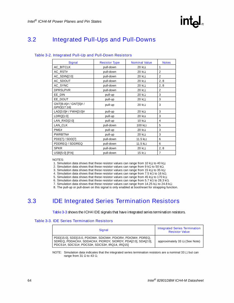
64 Intel® 82801DBM ICH4-M Datasheet
Intel® ICH4-M Power Planes and Pin States
3.2 Integrated Pull-Ups and Pull-Downs
NOTES:1. Simulation data shows that these resistor values can range from 10 k to 40 k .2. Simulation data shows that these resistor values can range from 9 k to 50 k .3. Simulation data shows that these resistor values can range from 15 k to 35 k4. Simulation data shows that these resistor values can range from 7.5 k to 16 k .5. Simulation data shows that these resistor values can range from 45 k to 170 k6. Simulation data shows that these resistor values can range from 5.7 k to 28.3 k .7. Simulation data shows that these resistor values can range from 14.25 k to 24.8 k8. The pull-up or pull-down on this signal is only enabled at boot/reset for strapping function.
3.3 IDE Integrated Series Termination ResistorsTable 3-3 shows the ICH4 IDE signals that have integrated series termination resistors.
NOTE: Simulation data indicates that the integrated series termination resistors are a nominal 33 but can range from 31 to 43 .
Table 3-2. Integrated Pull-Up and Pull-Down Resistors
Signal Resistor Type Nominal Value NotesAC_BITCLK pull-down 20 k 1AC_RST# pull-down 20 k 2AC_SDIN[2:0] pull-down 20 k 2AC_SDOUT pull-down 20 k 2, 8AC_SYNC pull-down 20 k 2, 8DPRSLPVR pull-down 20 k 2EE_DIN pull-up 20 k 3EE_DOUT pull-up 20 k 3GNT[B:A]# / GNT[5]# / GPIO[17:16]
pull-up 20 k 3
LAD[3:0]# / FWH[3:0]# pull-up 20 k 3LDRQ[1:0] pull-up 20 k 3LAN_RXD[2:0] pull-up 10 k 4LAN_CLK pull-down 100 k 5PME# pull-up 20 k 3PWRBTN# pull-up 20 k 3PDD[7] / SDD[7] pull-down 11.5 k 6PDDREQ / SDDREQ pull-down 11.5 k 6SPKR pull-down 20 k 2, 8USB[5:0] [P,N] pull-down 15 k 7
Table 3-3. IDE Series Termination Resistors
Signal Integrated Series Termination Resistor Value
PDD[15:0], SDD[15:0, PDIOW#, SDIOW#, PDIOR#, PDIOW#, PDREQ, SDREQ, PDDACK#, SDDACK#, PIORDY, SIORDY, PDA[2:0], SDA[2:0], PDCS1#, SDCS1#, PDCS3#, SDCS3#, IRQ14, IRQ15]
approximately 33 (See Note)

Intel® 82801DBM ICH4-M Datasheet 65
Intel® ICH4-M Power Planes and Pin States
3.4 Output and I/O Signals Planes and StatesTable 3-4 shows the power plane associated with the output and I/O signals, as well as the state at various times. Within the table, the following terms are used:
�High-Z� Tri-state. ICH4 not driving the signal high or low.
�High� ICH4 is driving the signal to a logic �1�
�Low� ICH4 is driving the signal to a logic �0�
�Defined� Driven to a level that is defined by the function (will be high or low)
�Undefined� ICH4 is driving the signal, but the value is indeterminate.
�Running� Clock is toggling or signal is transitioning because function not stopping
�Off� The power plane is off, so ICH4 is not driving
Note that the signal levels are the same in S4 and S5.

66 Intel® 82801DBM ICH4-M Datasheet
Intel® ICH4-M Power Planes and Pin States
Table 3-4. Power Plane and States for Output and I/O Signals (Sheet 1 of 3)
Signal Name Power Plane
During PCIRST#6 /RSMRST#7
Immediately after PCIRST#6
/ RSMRST#7C3/C4 S1-M S3 S4/S5
PCI Bus
AD[31:0] Main I/O High-Z Undefined Defined Defined Off Off
C/BE[3:0]# Main I/O High-Z Undefined Defined Defined Off Off
CLKRUN# Main I/O Low Low Defined Off Off
DEVSEL# Main I/O High-Z High-Z High-Z High-Z Off Off
FRAME# Main I/O High-Z High-Z High-Z High-Z Off Off
GNT[0:4]# Main I/O High High High High Off Off
GNT[A:B]# Main I/O High-Z High High High Off Off
IRDY#, TRDY# Main I/O High-Z High-Z High-Z High-Z Off Off
PAR Main I/O High-Z Undefined Defined Defined Off Off
PCIRST# Resume I/O Low High High High Low Low
PERR# Main I/O High-Z High-Z High-Z High-Z Off Off
PLOCK# Main I/O High-Z High-Z High-Z High-Z Off Off
STOP# Main I/O High-Z High-Z High-Z High-Z Off Off
LPC Interface
LAD[3:0] Main I/O High High High Defined Off Off
LFRAME# Main I/O High High High High Off Off
LAN Connect and EEPROM Interface
EE_CS LAN I/O Low Running Defined Defined Note 4 Note 4
EE_DOUT LAN I/O High High Defined Defined Note 4 Note 4
EE_SHCLK LAN I/O Low Running Defined Defined Note 4 Note 4
LAN_RSTSYNC LAN I/O High Defined Defined Defined Note 4 Note 4
LAN_TXD[2:0] LAN I/O Low Defined Defined Defined Note 4 Note 4
IDE Interface
PDA[2:0], SDA[2:0] Main I/O Undefined Undefined Undefined Off Off Off
PDCS1#, PDCS3# Main I/O High High High High Off Off
PDD[15:8], SDD[15:8], PDD[6:0], SDD[6:0]
Main I/O High-Z High-Z Defined Off Off Off
PDD[7], SDD[7] Main I/O Low Low Defined Off Off Off
PDDACK#, SDDACK# Main I/O High High High Off Off Off
PDIOR#, PDIOW# Main I/O High High High Off Off Off
SDCS1#, SDCS3# Main I/O High High High Off Off Off
SDIOR#, SDIOW# Main I/O High High High Off Off Off
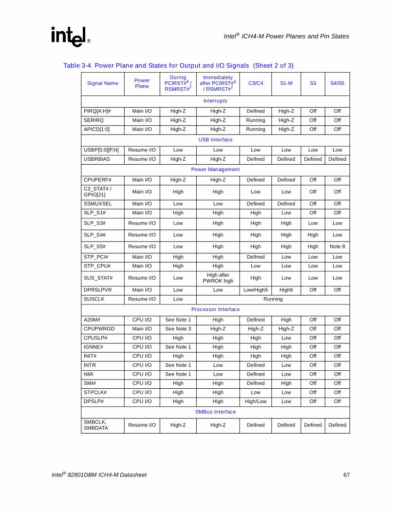
Intel® 82801DBM ICH4-M Datasheet 67
Intel® ICH4-M Power Planes and Pin States
Interrupts
PIRQ[A:H]# Main I/O High-Z High-Z Defined High-Z Off Off
SERIRQ Main I/O High-Z High-Z Running High-Z Off Off
APICD[1:0] Main I/O High-Z High-Z Running High-Z Off Off
USB Interface
USBP[5:0][P,N] Resume I/O Low Low Low Low Low Low
USBRBIAS Resume I/O High-Z High-Z Defined Defined Defined Defined
Power Management
CPUPERF# Main I/O High-Z High-Z Defined Defined Off Off
C3_STAT# / GPIO[21] Main I/O High High Low Low Off Off
SSMUXSEL Main I/O Low Low Defined Defined Off Off
SLP_S1# Main I/O High High High Low Off Off
SLP_S3# Resume I/O Low High High High Low Low
SLP_S4# Resume I/O Low High High High High Low
SLP_S5# Resume I/O Low High High High High Note 8
STP_PCI# Main I/O High High Defined Low Low Low
STP_CPU# Main I/O High High Low Low Low Low
SUS_STAT# Resume I/O Low High after PWROK high High Low Low Low
DPRSLPVR Main I/O Low Low Low/High5 High6 Off Off
SUSCLK Resume I/O Low Running
Processor Interface
A20M# CPU I/O See Note 1 High Defined High Off Off
CPUPWRGD Main I/O See Note 3 High-Z High-Z High-Z Off Off
CPUSLP# CPU I/O High High High Low Off Off
IGNNE# CPU I/O See Note 1 High High High Off Off
INIT# CPU I/O High High High High Off Off
INTR CPU I/O See Note 1 Low Defined Low Off Off
NMI CPU I/O See Note 1 Low Defined Low Off Off
SMI# CPU I/O High High Defined High Off Off
STPCLK# CPU I/O High High Low Low Off Off
DPSLP# CPU I/O High High High/Low Low Off Off
SMBus Interface
SMBCLK, SMBDATA Resume I/O High-Z High-Z Defined Defined Defined Defined
Table 3-4. Power Plane and States for Output and I/O Signals (Sheet 2 of 3)
Signal Name Power Plane
During PCIRST#6 /RSMRST#7
Immediately after PCIRST#6
/ RSMRST#7C3/C4 S1-M S3 S4/S5
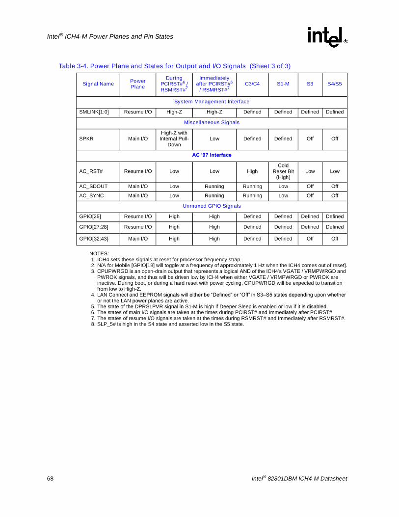
68 Intel® 82801DBM ICH4-M Datasheet
Intel® ICH4-M Power Planes and Pin States
NOTES:1. ICH4 sets these signals at reset for processor frequency strap.2. N/A for Mobile [GPIO[18] will toggle at a frequency of approximately 1 Hz when the ICH4 comes out of reset].3. CPUPWRGD is an open-drain output that represents a logical AND of the ICH4�s VGATE / VRMPWRGD and
PWROK signals, and thus will be driven low by ICH4 when either VGATE / VRMPWRGD or PWROK are inactive. During boot, or during a hard reset with power cycling, CPUPWRGD will be expected to transition from low to High-Z.
4. LAN Connect and EEPROM signals will either be �Defined� or �Off� in S3�S5 states depending upon whether or not the LAN power planes are active.
5. The state of the DPRSLPVR signal in S1-M is high if Deeper Sleep is enabled or low if it is disabled.6. The states of main I/O signals are taken at the times during PCIRST# and Immediately after PCIRST#.7. The states of resume I/O signals are taken at the times during RSMRST# and Immediately after RSMRST#.8. SLP_5# is high in the S4 state and asserted low in the S5 state.
System Management Interface
SMLINK[1:0] Resume I/O High-Z High-Z Defined Defined Defined Defined
Miscellaneous Signals
SPKR Main I/OHigh-Z with Internal Pull-
DownLow Defined Defined Off Off
AC �97 Interface
AC_RST# Resume I/O Low Low HighCold
Reset Bit (High)
Low Low
AC_SDOUT Main I/O Low Running Running Low Off Off
AC_SYNC Main I/O Low Running Running Low Off Off
Unmuxed GPIO Signals
GPIO[25] Resume I/O High High Defined Defined Defined Defined
GPIO[27:28] Resume I/O High High Defined Defined Defined Defined
GPIO[32:43} Main I/O High High Defined Defined Off Off
Table 3-4. Power Plane and States for Output and I/O Signals (Sheet 3 of 3)
Signal Name Power Plane
During PCIRST#6 /RSMRST#7
Immediately after PCIRST#6
/ RSMRST#7C3/C4 S1-M S3 S4/S5

Intel® 82801DBM ICH4-M Datasheet 69
Intel® ICH4-M Power Planes and Pin States
3.5 Power Planes for Input SignalsTable 3-5 shows the power plane associated with each input signal, as well as what device drives the signal at various times. Valid states include:
� High
� Low
� Static: Will be high or low, but will not change
� Driven: Will be high or low, and is allowed to change
� Running: For input clocks
Table 3-5. Power Plane for Input Signals (Sheet 1 of 2)
Signal Name Power Well Driver During Reset C3 S1-M S3 S5
BATLOW# Resume I/O Power Supply High High High High
A20GATE Main I/O External Microcontroller Static Static Low Low
AC_BIT_CLK Main I/O AC �97 Codec Driven Low Low Low
AC_SDIN[2:0] Resume I/O AC �97 Codec Driven Low Low Low
AGPBUSY# Main I/O AGP Component Driven High Low Low
APICCLK Main I/O Clock Generator Running Low Low Low
CLK14 Main I/O Clock Generator Running Low Low Low
CLK48 Main I/O Clock Generator Running Low Low Low
CLK66 Main Logic Clock Generator Running Low Low Low
EE_DIN LAN I/O EEPROM Component Driven Driven Note 1 Note 1
FERR# CPU I/O External Pull-Up Static Static High High
INTRUDER# RTC External Switch Driven Driven Driven Driven
IRQ[15:14] Main I/O IDE Driven Static Low Low
LAN_CLK LAN I/O LAN Connect Component Driven Driven Note 1 Note 1
LAN_RST# Resume I/O Power Supply High High Static Static
LAN_RXD[2:0] LAN I/O LAN Connect Component Driven Driven Note 1 Note 1
LDRQ[0]# Main I/O LPC Devices Driven High Low Low
LDRQ[1]# Main I/O LPC Devices Driven High Low Low
OC[5:0]# Resume I/O External Pull-Ups Driven Driven Driven Driven
PCICLK Main I/O Clock Generator Running Low Low Low
PDDREQ Main I/O IDE Device Driven Static Low Low
PIORDY Main I/O IDE Device Static Static Low Low
PME# Resume I/O Internal Pull-Up Driven Driven Driven Driven
PWRBTN# Resume I/O Internal Pull-Up Driven Driven Driven Driven
PWROK RTC System Power Supply Driven Driven Low Low
RCIN# Main I/O External Microcontroller High High Low Low
REQ[0:5]# Main I/O PCI Master Driven Driven Low Low
REQ[B:A]# Main I/O PC/PCI Devices Driven Driven Low Low

70 Intel® 82801DBM ICH4-M Datasheet
Intel® ICH4-M Power Planes and Pin States
NOTES:1. LAN Connect and EEPROM signals will either be �Driven� or �Low� in S3�S5 states depending upon whether
or not the LAN power planes are active.
RI# Resume I/O Serial Port Buffer Driven Driven Driven Driven
RSMRST# RTC External RC Circuit High High High High
RTCRST# RTC External RC Circuit High High High High
SDDREQ Main I/O IDE Drive Driven Static Low Low
SERR# Main I/O PCI Bus Peripherals Driven High Low Low
SIORDY Main I/O IDE Drive Driven Static Low Low
SMBALERT# Resume I/O External Pull-Up Driven Driven Driven Driven
SYS_RESET# Resume I/O External Circuit Driven Driven Driven Driven
THRM# Main I/O Thermal Sensor Driven Driven Low Low
THRMTRIP# CPU I/O External Pull-Up Driven Driven High High
USBRBIAS# Resume I/O External Pull-Down Driven Driven Driven Driven
VGATE / VRMPWRGD Main I/O CPU Voltage Regulator Driven Driven Low Low
Table 3-5. Power Plane for Input Signals (Sheet 2 of 2)
Signal Name Power Well Driver During Reset C3 S1-M S3 S5

Intel® 82801DBM ICH4-M Datasheet 71
Intel® ICH4-M System Clock Domains
4 Intel® ICH4-M System Clock Domains
Table 4-1 shows the system clock domains. Figure 4-1 shows the assumed connection of the various system components, including the clock generator. For complete details of the system clocking solution refer to the system�s clock generator component specification.
Table 4-1. Intel® ICH4-M and System Clock Domains
Clock Domain Frequency Source Usage
ICH4CLK66 66 MHz Main Clock
GeneratorHub I/F, processor I/F. AGP. Shut off during S1-M or below.
ICH4PCICLK 33 MHz Main Clock
GeneratorFree-running PCI Clock to ICH4. This clock remains on during S0 state, and is expected to be shut off during S1-M or below.
System PCI 33 MHz Main Clock Generator
PCI Bus, LPC I/F. These only go to external PCI and LPC devices. Will stop based on CLKRUN# (and STP_PCI#).
ICH4CLK48 48 MHz Main Clock
GeneratorSuper I/O, USB Controllers. Expected to be shut off during S1-M or below.
ICH4CLK14 14.31818 MHz Main Clock
GeneratorUsed for ACPI timer. Expected to be shut off during S1-M or below.
ICH4 AC_BIT_CLK 12.288 MHz AC �97 Codec
AC�97 Link. Generated by AC �97 Codec. Can be shut by codec in D3. Expected to be shut off during S1-M or below.
ICH4APICCLK 33 MHz Main Clock
GeneratorUsed for ICH4-CPU interrupt messages. Runs up to 33 MHz. Expected to be shut off during S1-M or below.
LAN_CLK 5 to 50 MHz LAN Connect Component
Generated by the LAN Connect component. Expected to be shut off during S1-M or below.

72 Intel® 82801DBM ICH4-M Datasheet
Intel® ICH4-M System Clock Domains
Figure 4-1. Conceptual System Clock Diagram
32 kHzXTAL
ICH4
SLP_S1#
LAN Connect50 MHz
12.288 MHz
66 MHz
33 MHzAPIC CLK14.31818 MHz48 MHzSTP_CPU#
STP_PCI#
AC�97 Codec(s)
SUSCLK (32 kHz)
ClockGen.
PCI Clocks
(33 MHz)
14.31818 MHz
48 MHz

Intel® 82801DBM ICH4-M Datasheet 73
Functional Description
5 Functional Description
This chapter describes the functions and interfaces of the ICH4.
5.1 Hub Interface to PCI Bridge (D30:F0)The hub interface to PCI Bridge resides in PCI Device 30, Function 0 on bus #0. This portion of the ICH4 implements the buffering and control logic between PCI and the hub interface. The arbitration for the PCI bus is handled by this PCI device. The PCI decoder in this device must decode the ranges for the hub interface. All register contents will be lost when core well power is removed.
5.1.1 PCI Bus InterfaceThe ICH4 PCI interface provides a 33-MHz, PCI Local Bus Specification, Revision 2.2-compliant implementation. All PCI signals are 5-V tolerant. The ICH4 integrates a PCI arbiter that supports up to six external PCI bus masters in addition to the internal ICH4 requests.
Note that most transactions targeted to the ICH4 will first appear on the external PCI bus before being claimed back by the ICH4. The exceptions are I/O cycles involving USB, IDE, and AC �97. These transactions will complete over the hub interface without appearing on the external PCI bus. Configuration cycles targeting USB, IDE, or AC �97 will appear on the PCI bus. If the ICH4 is programmed for positive decode, the ICH4 will claim the cycles appearing on the external PCI bus in medium decode time. If the ICH4 is programmed for subtractive decode, the ICH4 will claim these cycles in subtractive time. If the ICH4 is programmed for subtractive decode, these cycles can be claimed by another positive decode agent out on PCI. This architecture enables the ability to boot off of a PCI card that positively decodes the boot cycles. In order to boot off a PCI card it is necessary to keep the ICH4 in subtractive decode mode. When booting off a PCI card, the BOOT_STS bit (bit 2, TCO2 Status Register) will be set.
Note: The ICH4�s AC �97, IDE and USB Controllers cannot perform peer-to-peer traffic.
Note: Devices on the ICH4 PCI bus (other than the ICH4) are not permitted to assert the PLOCK# signal.
Note: Poor performing PCI devices that cause long latencies (numerous retries) to processor-to-PCI Locked cycles may starve isochronous transfers between USB or AC �97 devices and memory. This will result in overrun or underrun, causing reduced quality of the isochronous data (e.g., audio).
Note: PCI configuration write cycles, initiated by the processor, with the following characteristics will be converted to a Special Cycle with the Shutdown message type.
� Device Number (AD[15:11]) = 11111� Function Number (AD[10:8]) = 111� Register Number (AD[7:2]) = 000000� Data = 00h� Bus number matches secondary bus number

74 Intel® 82801DBM ICH4-M Datasheet
Functional Description
Note: If the processor issues a locked cycle to a resource that is too slow (e.g., PCI), the ICH4 will not allow upstream requests to be performed until the cycle completion. This may be critical for isochronous buses which assume certain timing for their data flow (e.g., AC �97 or USB). Devices on these buses may suffer from underrun if the asynchronous traffic is too heavy. Underrun means that the same data is sent over the bus while ICH4 is not able to issue a request for the next data. Snoop cycles are not permitted while the front side bus is locked.
Note: Locked cycles are assumed to be rare. Locks by PCI targets are assumed to exist for a short duration (a few microseconds at most). If a system has a very large number of locked cycles and some that are very long, then the system will definitely experience underruns and overruns. The units most likely to have problems are the AC �97 controller and the USB controllers. Other units could get underruns/overruns, but are much less likely. The IDE controller (due to its stalling capability on the cable) should not get any underruns or overruns.
Note: PCI Bus Masters should not use memory area locations as a target if that area is programmed to be anything but Read/Write.
5.1.2 PCI-to-PCI Bridge ModelFrom a software perspective, the ICH4 contains a PCI-to-PCI bridge. This bridge connects the hub interface to the PCI bus. By using the PCI-to-PCI bridge software model, the ICH4 can have its decode ranges programmed by existing plug-and-play software such that PCI ranges do not conflict with AGP and graphics aperture ranges in the Host controller.
5.1.3 IDSEL to Device Number MappingWhen addressing devices on the external PCI bus (with the PCI slots) the ICH4 will assert one address signal as an IDSEL. When accessing device 0, the ICH4 will assert AD16. When accessing Device 1, the ICH4 will assert AD17. This mapping continues all the way up to device 15 where the ICH4 asserts AD31. Note that the ICH4�s internal functions (AC �97, IDE, USB, and PCI Bridge) are enumerated like they are on a separate PCI bus (the hub interface) from the external PCI bus. The integrated LAN Controller is Device 8 on the ICH4�s PCI bus, and hence it uses AD24 for IDSEL.
5.1.4 SERR# FunctionalityThere are several internal and external sources that can cause SERR#. The ICH4 can be programmed to cause an NMI based on detecting that an SERR# condition has occurred. The NMI can also be routed to instead cause an SMI#. Note that the ICH4 does not drive the external PCI bus SERR# signal active onto the PCI bus. The external SERR# signal is an input into the ICH4 driven only by external PCI devices. The conceptual logic diagrams in Figure 5-1 and Figure 5-2 illustrate all sources of SERR#, along with their respective enable and status bits. Figure 5-3 shows how the ICH4 error reporting logic is configured for NMI# generation.
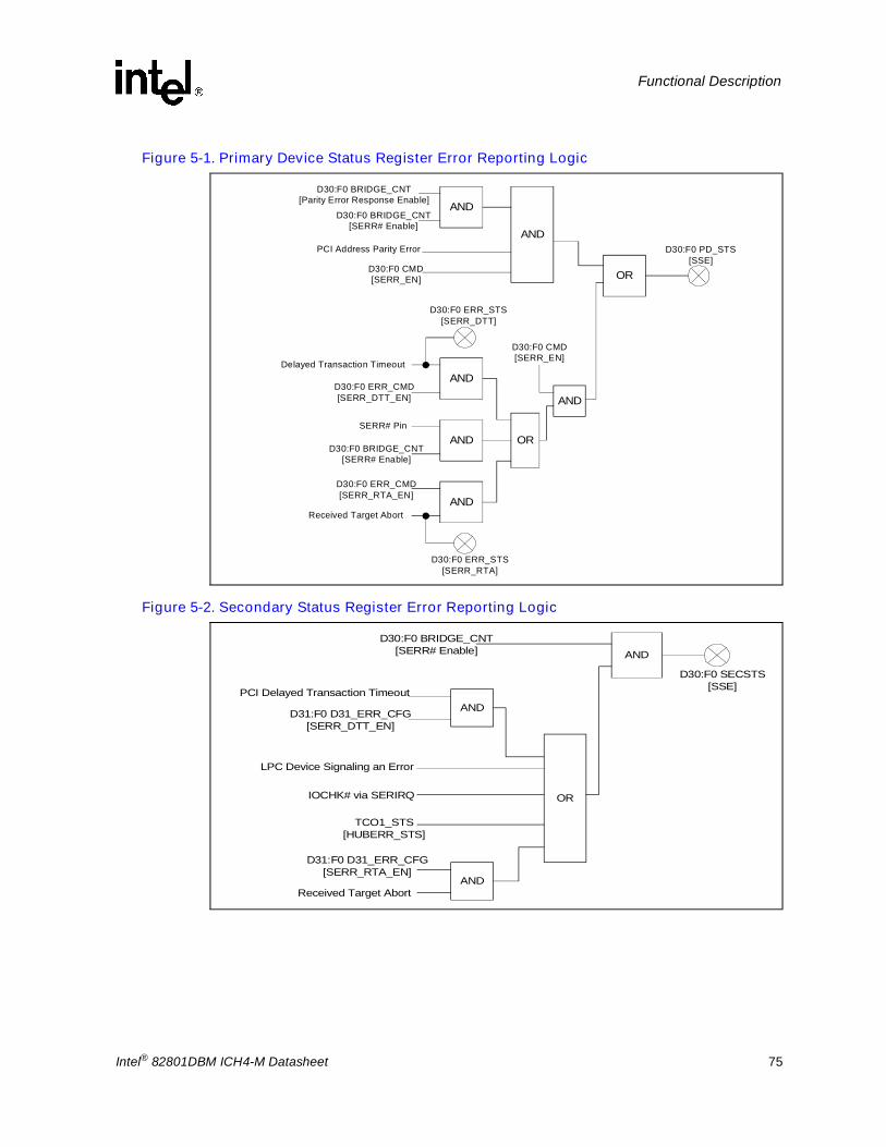
Intel® 82801DBM ICH4-M Datasheet 75
Functional Description
Figure 5-1. Primary Device Status Register Error Reporting Logic
Figure 5-2. Secondary Status Register Error Reporting Logic
AND
OR
ANDD30:F0 BRIDGE_CNT
[Parity Error Response Enable]D30:F0 BRIDGE_CNT
[SERR# Enable]
PCI Address Parity Error
D30:F0 CMD[SERR_EN]
D30:F0 PD_STS[SSE]
AND
AND
AND
AND
OR
Delayed Transaction Timeout
D30:F0 ERR_CMD[SERR_DTT_EN]
SERR# Pin
D30:F0 BRIDGE_CNT[SERR# Enable]
D30:F0 ERR_CMD[SERR_RTA_EN]
Received Target Abort
D30:F0 ERR_STS[SERR_DTT]
D30:F0 CMD[SERR_EN]
D30:F0 ERR_STS[SERR_RTA]
AND
OR
AND
AND
D30:F0 SECSTS[SSE]
D30:F0 BRIDGE_CNT[SERR# Enable]
PCI Delayed Transaction Timeout
D31:F0 D31_ERR_CFG[SERR_DTT_EN]
LPC Device Signaling an Error
IOCHK# via SERIRQ
TCO1_STS[HUBERR_STS]
D31:F0 D31_ERR_CFG[SERR_RTA_EN]
Received Target Abort
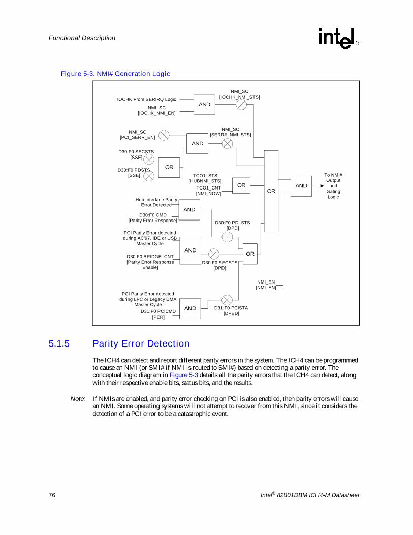
76 Intel® 82801DBM ICH4-M Datasheet
Functional Description
5.1.5 Parity Error DetectionThe ICH4 can detect and report different parity errors in the system. The ICH4 can be programmed to cause an NMI (or SMI# if NMI is routed to SMI#) based on detecting a parity error. The conceptual logic diagram in Figure 5-3 details all the parity errors that the ICH4 can detect, along with their respective enable bits, status bits, and the results.
Note: If NMIs are enabled, and parity error checking on PCI is also enabled, then parity errors will cause an NMI. Some operating systems will not attempt to recover from this NMI, since it considers the detection of a PCI error to be a catastrophic event.
Figure 5-3. NMI# Generation Logic
ANDIOCHK From SERIRQ Logic
NMI_SC[IOCHK_NMI_EN]
AND
To NMI#Output
andGatingLogic
OR
NMI_SC[IOCHK_NMI_STS]
AND
NMI_SC[SERR#_NMI_STS]NMI_SC
[PCI_SERR_EN]
OR
D30:F0 SECSTS[SSE]
D30:F0 PDSTS[SSE]
ORAND
OR
TCO1_STS[HUBNMI_STS]
TCO1_CNT[NMI_NOW]
NMI_EN[NMI_EN]
D30:F0 PD_STS[DPD]
D30:F0 SECSTS[DPD]
PCI Parity Error detectedduring AC'97, IDE or USB
Master Cycle
D30:F0 BRIDGE_CNT[Parity Error Response
Enable]
AND D31:F0 PCISTA[DPED]
PCI Parity Error detectedduring LPC or Legacy DMA
Master CycleD31:F0 PCICMD
[PER]
AND
Hub Interface ParityError Detected
D30:F0 CMD[Parity Error Response]

Intel® 82801DBM ICH4-M Datasheet 77
Functional Description
5.1.6 Standard PCI Bus Configuration MechanismThe PCI Bus defines a slot based �configuration space� that allows each device to contain up to eight functions with each function containing up to 256, 8-bit configuration registers. The PCI specification defines two bus cycles to access the PCI configuration space: Configuration Read and Configuration Write. Memory and I/O spaces are supported directly by the processor. Configuration space is supported by a mapping mechanism implemented within the ICH4. The PCI specification defines two mechanisms to access configuration space, Mechanism #1 and Mechanism #2. The ICH4 only supports Mechanism #1.
Configuration cycles for PCI Bus #0 devices #2 through #31, and for PCI Bus numbers greater than 0 will be sent towards the ICH4 from the host controller. The ICH4 compares the non-zero Bus Number with the Secondary Bus Number and Subordinate Bus number registers of its PCI-to-PCI bridge to determine if the configuration cycle is meant for Primary PCI or a downstream PCI bus.
Note: Configuration writes to internal ICH4 USB EHCI (D29:F7) and AC �97 (D31:F5, F6) devices when disabled are illegal and may cause undefined results.
5.1.6.1 Type 0 to Type 0 Forwarding
When a Type 0 configuration cycle is received on hub interface to any function other than USB EHCI or AC �97, the ICH4 forwards these cycles to PCI and then reclaims them. The ICH4 uses address bits AD[15:13] to communicate the ICH4 device numbers in Type 0 configuration cycles. If the Type 0 cycle on hub interface specifies any device number other than 29, 30 or 31, the ICH4 will not set any address bits in the range AD[31:11] during the corresponding transaction on PCI. Table 5-1 shows the device number translation.
The ICH4 logic will generate single DWord configuration read and write cycles on the PCI bus. The ICH4 will generate a Type 0 configuration cycle for configurations to the bus number matching the PCI bus. Type 1 configuration cycles will be converted to Type 0 cycles in this case. If the cycle is targeting a device behind an external bridge, the ICH4 will run a Type 1 cycle on the PCI bus.
5.1.6.2 Type 1 to Type 0 Conversion
When the bus number for the Type 1 configuration cycle matches the PCI (Secondary) bus number, the ICH4 will convert the address as follows:
1. For device numbers 0 through 15, only one bit of the PCI address [31:16] will be set. If the device number is 0, AD[16] is set; if the device number is 1, AD[17] is set; etc.
2. The ICH4 will always drive 0s on bits AD[15:11] when converting Type 1 configurations cycles to Type 0 configuration cycles on PCI.
3. Address bits [10:1] will also be passed unchanged to PCI.4. Address bit 0 will be changed to 0.
Table 5-1. Type 0 Configuration Cycle Device Number Translation
Device # In Hub Interface Type 0 Cycle AD[31:11] During Address Phase of Type 0 Cycle on PCI
0 through 28 0000000000000000_00000b
29 0000000000000000_00100b
30 0000000000000000_01000b
31 0000000000000000_10000b

78 Intel® 82801DBM ICH4-M Datasheet
Functional Description
5.2 LAN Controller (B1:D8:F0)The ICH4�s integrated LAN Controller includes a 32-bit PCI controller that provides enhanced scatter-gather bus mastering capabilities and enables the LAN Controller to perform high-speed data transfers over the PCI bus. Its bus master capabilities enable the component to process high level commands and perform multiple operations, which lowers processor utilization by off-loading communication tasks from the processor. Two large transmit and receive FIFOs of 3 KB each help prevent data underruns and overruns while waiting for bus accesses. This enables the integrated LAN Controller to transmit data with minimum interframe spacing (IFS).
The ICH4 integrated LAN Controller can operate in either full-duplex or half-duplex mode. In full- duplex mode the LAN Controller adheres with the IEEE 802.3x Flow Control specification. Half duplex performance is enhanced by a proprietary collision reduction mechanism.
The integrated LAN Controller also includes an interface to a serial (4-pin) EEPROM. The EEPROM provides power-on initialization for hardware and software configuration parameters.
From a software perspective, the integrated LAN Controller appears to reside on the secondary side of the ICH4�s virtual PCI-to-PCI Bridge (see Section 5.1.2). This is typically Bus 1, but may be assigned a different number, depending on system configuration.
The following summarizes the ICH4 LAN Controller features:
� Compliance with Advanced Configuration and Power Interface and PCI Power Management standards
� Support for wake-up on interesting packets and link status change� Support for remote power-up using Wake on LAN* (WOL) technology� Deep power-down mode support� Support of Wired for Management (WfM) Rev 2.0� Backward compatible software with 82557, 82558, and 82559� TCP/UDP checksum off load capabilities� Support for Intel�s Adaptive Technology
5.2.1 LAN Controller Architectural OverviewFigure 5-4 is a high level block diagram of the ICH4 integrated LAN Controller. It is divided into four main subsystems: a Parallel subsystem, a FIFO subsystem and the Carrier-Sense Multiple Access with Collision Detect (CSMA/CD) unit.

Intel® 82801DBM ICH4-M Datasheet 79
Functional Description
5.2.1.1 Parallel Subsystem Overview
The parallel subsystem is broken down into several functional blocks: a PCI bus master interface, a micromachine processing unit and its corresponding microcode ROM, and a PCI Target Control/EEPROM/ interface. The parallel subsystem also interfaces to the FIFO subsystem, passing data (such as transmit, receive, and configuration data) and command and status parameters between these two blocks.
The PCI bus master interface provides a complete interface to the PCI bus and is compliant with the PCI Local Bus Specification, Revision 2.2. The LAN Controller provides 32 bits of addressing and data, as well as the complete control interface to operate on the PCI bus. As a PCI target, it follows the PCI configuration format which allows all accesses to the LAN Controller to be automatically mapped into free memory and I/O space upon initialization of a PCI system. For processing of transmit and receive frames, the integrated LAN Controller operates as a master on the PCI bus, initiating zero wait-state transfers for accessing these data parameters.
The LAN Controller Control/Status Register Block is part of the PCI target element. The Control/Status Register block consists of the following LAN Controller internal control registers: System Control Block (SCB), PORT, EEPROM Control, and Management Data Interface (MDI) Control.
The micromachine is an embedded processing unit contained in the LAN Controller that enables Adaptive Technology. The micromachine accesses the LAN Controller�s microcode ROM, working its way through the opcodes (or instructions) contained in the ROM to perform its functions. Parameters accessed from memory (e.g., pointers to data buffers) are also used by the micromachine during the processing of transmit or receive frames by the LAN Controller. A typical micromachine function is to transfer a data buffer pointer field to the LAN Controller�s DMA unit for direct access to the data buffer. The micromachine is divided into two units, Receive Unit and Command Unit which includes transmit functions. These two units operate independently and concurrently. Control is switched between the two units according to the microcode instruction flow. The independence of the Receive and Command units in the micromachine allows the LAN Controller to execute commands and receive incoming frames simultaneously, with no real-time processor intervention.
Figure 5-4. Integrated LAN Controller Block Diagram
CSMA/CDUnit
Data Interface Unit(DIU)
Four ChannelAddressing Unit -
DMA
PCI BusInterface Unit
(BIU)
PCI Target andEEPROM Interface
Micro-machine
DualPortedFIFO
3 KbyteRx FIFO
FIFO Control
3 KbyteTx FIFO
EEPROMInterface
PCIInterface
LANConnectInterface

80 Intel® 82801DBM ICH4-M Datasheet
Functional Description
The LAN Controller contains an interface to an external serial EEPROM. The EEPROM is used to store relevant information for a LAN connection such as node address, as well as board manufacturing and configuration information. Both read and write accesses to the EEPROM are supported by the LAN Controller. Information on the EEPROM interface is detailed in Section 5.2.3.
5.2.1.2 FIFO Subsystem Overview
The ICH4 LAN Controller FIFO subsystem consists of a 3-kB transmit FIFO and 3-KB receive FIFO. Each FIFO is unidirectional and independent of the other. The FIFO subsystem serves as the interface between the LAN Controller parallel side and the serial CSMA/CD unit. It provides a temporary buffer storage area for frames as they are either being received or transmitted by the LAN Controller, which improves performance:
� Transmit frames can be queued within the transmit FIFO, allowing back-to-back transmission within the minimum Interframe Spacing (IFS).
� The storage area in the FIFO allows the LAN Controller to withstand long PCI bus latencies without losing incoming data or corrupting outgoing data.
� The ICH4 LAN Controller�s transmit FIFO threshold allows the transmit start threshold to be tuned to eliminate underruns while concurrent transmits are being performed.
� The FIFO subsection allows extended PCI zero wait-state burst accesses to or from the LAN Controller for both transmit and receive frames since the transfer is to the FIFO storage area rather than directly to the serial link.
� Transmissions resulting in errors (collision detection or data underrun) are retransmitted directly from the LAN Controller�s FIFO, increasing performance and eliminating the need to re-access this data from the host system.
� Incoming runt receive frames (in other words, frames that are less than the legal minimum frame size) can be discarded automatically by the LAN Controller without transferring this faulty data to the host system.
5.2.1.3 Serial CSMA/CD Unit Overview
The CSMA/CD unit of the ICH4 LAN Controller allows it to be connected to the 82562ET/EM 10/100 Mbps Ethernet LAN Connect components. The CSMA/CD unit performs all of the functions of the 802.3 protocol (e.g., frame formatting, frame stripping, collision handling, deferral to link traffic, etc.). The CSMA/CD unit can also be placed in a full-duplex mode, which allows simultaneous transmission and reception of frames.

Intel® 82801DBM ICH4-M Datasheet 81
Functional Description
5.2.2 LAN Controller PCI Bus InterfaceAs a Fast Ethernet Controller, the role of the ICH4 integrated LAN Controller is to access transmitted data or deposit received data. The LAN Controller, as a bus master device, will initiate memory cycles via the PCI bus to fetch or deposit the required data.
To perform these actions, the LAN Controller is controlled and examined by the processor via its control and status structures and registers. Some of these control and status structures reside in the LAN Controller and some reside in system memory. For access to the LAN Controller�s Control/Status Registers (CSR), the LAN Controller acts as a slave (in other words, a target device). The LAN Controller serves as a slave also while the processor accesses the EEPROM.
5.2.2.1 Bus Slave Operation
The ICH4 integrated LAN Controller serves as a target device in one of the following cases:
� Processor accesses to the LAN Controller System Control Block (SCB) Control/Status Registers (CSR)
� Processor accesses to the EEPROM through its CSR
� Processor accesses to the LAN Controller PORT address via the CSR
� Processor accesses to the MDI control register in the CSR
The size of the CSR memory space is 4 kB in the memory space and 64 bytes in the I/O space. The LAN Controller treats accesses to these memory spaces differently.
Control/Status Register (CSR) Accesses
The integrated LAN Controller supports zero wait-state single cycle memory or I/O mapped accesses to its CSR space. Separate BARs request 4 kB of memory space and 64 bytes of I/O space to accomplish this. Based on its needs, the software driver will use either memory or I/O mapping to access these registers. The LAN Controller provides four valid Kbytes of CSR space, which include the following elements:
� System Control Block (SCB) registers
� PORT register
� EEPROM control register
� MDI control register
� Flow control registers
In the case of accessing the Control/Status Registers, the processor is the initiator and the LAN Controller is the target.
Read Accesses: The processor, as the initiator, drives address lines AD[31:0], the command and byte enable lines C/BE[3:0]# and the control lines IRDY# and FRAME#. As a slave, the LAN Controller controls the TRDY# signal and provides valid data on each data access. The LAN Controller allows the processor to issue only one read cycle when it accesses the Control/Status Registers, generating a disconnect by asserting the STOP# signal. The processor can insert wait-states by deasserting IRDY# when it is not ready.

82 Intel® 82801DBM ICH4-M Datasheet
Functional Description
Write Accesses: The processor, as the initiator, drives the address lines AD[31:0], the command and byte enable lines C/BE[3:0]# and the control lines IRDY# and FRAME#. It also provides the LAN Controller with valid data on each data access immediately after asserting IRDY#. The LAN Controller controls the TRDY# signal and asserts it from the data access. The LAN Controller allows the processor to issue only one I/O write cycle to the Control/Status Registers, generating a disconnect by asserting the STOP# signal. This is true for both memory mapped and I/O mapped accesses.
Retry Premature Accesses
The LAN Controller responds with a Retry to any configuration cycle accessing the LAN Controller before the completion of the automatic read of the EEPROM. The LAN Controller may continue to retry any configuration accesses until the EEPROM read is complete. The LAN Controller does not enforce the rule that the retried master must attempt to access the same address again in order to complete any delayed transaction. Any master access to the LAN Controller after the completion of the EEPROM read will be honored.
Error Handling
Data Parity Errors: The LAN Controller checks for data parity errors while it is the target of the transaction. If an error was detected, the LAN Controller always sets the Detected Parity Error bit in the PCI Configuration Status register, bit 15. The LAN Controller also asserts PERR#, if the Parity Error Response bit is set (PCI Configuration Command register, bit 6). The LAN Controller does not attempt to terminate a cycle in which a parity error was detected. This gives the initiator the option of recovery.
Target-Disconnect: The LAN Controller prematurely terminates a cycle in the following cases:
� After accesses to its CSR
� After accesses to the configuration space
System Error: The LAN Controller reports parity error during the address phase using the SERR# pin. If the SERR# Enable bit in the PCI Configuration Command register or the Parity Error Response bit are not set, the LAN Controller only sets the Detected Parity Error bit (PCI Configuration Status register, bit 15). If SERR# Enable and Parity Error Response bits are both set, the LAN Controller sets the Signaled System Error bit (PCI Configuration Status register, bit 14) as well as the Detected Parity Error bit and asserts SERR# for one clock.
The LAN Controller, when detecting system error, will claim the cycle if it was the target of the transaction and continue the transaction as if the address was correct.
Note: The LAN Controller reports a system error for any error during an address phase, whether or not it is involved in the current transaction.

Intel® 82801DBM ICH4-M Datasheet 83
Functional Description
5.2.2.2 Bus Master Operation
As a PCI Bus Master, the ICH4 integrated LAN Controller initiates memory cycles to fetch data for transmission or deposit received data and for accessing the memory resident control structures. The LAN Controller performs zero wait-state burst read and write cycles to the host main memory. For bus master cycles, the LAN Controller is the initiator and the host main memory (or the PCI host bridge, depending on the configuration of the system) is the target.
The processor provides the LAN Controller with action commands and pointers to the data buffers that reside in host main memory. The LAN Controller independently manages these structures and initiates burst memory cycles to transfer data to and from them. The LAN Controller uses the Memory Read Multiple (MR Multiple) command for burst accesses to data buffers and the Memory Read Line (MR Line) command for burst accesses to control structures. For all write accesses to the control structure, the LAN Controller uses the Memory Write (MW) command. For write accesses to data structure, the LAN Controller may use either the Memory Write or Memory Write and Invalidate (MWI) commands.
Read Accesses: The LAN Controller performs block transfers from host system memory in order to perform frame transmission on the serial link. In this case, the LAN Controller initiates zero wait-state memory read burst cycles for these accesses. The length of a burst is bounded by the system and the LAN Controller�s internal FIFO. The length of a read burst may also be bounded by the value of the Transmit DMA Maximum Byte Count in the Configure command. The Transmit DMA Maximum Byte Count value indicates the maximum number of transmit DMA PCI cycles that will be completed after an LAN Controller internal arbitration.
The LAN Controller, as the initiator, drives the address lines AD[31:0], the command and byte enable lines C/BE[3:0]# and the control lines IRDY# and FRAME#. The LAN Controller asserts IRDY# to support zero wait-state burst cycles. The target signals the LAN Controller that valid data is ready to be read by asserting the TRDY# signal.
Write Accesses: The LAN Controller performs block transfers to host system memory during frame reception. In this case, the LAN Controller initiates memory write burst cycles to deposit the data, usually without wait-states. The length of a burst is bounded by the system and the LAN Controller�s internal FIFO threshold. The length of a write burst may also be bounded by the value of the Receive DMA Maximum Byte Count in the Configure command. The Receive DMA Maximum Byte Count value indicates the maximum number of receive DMA PCI transfers that will be completed before the LAN Controller internal arbitration.
The LAN Controller, as the initiator, drives the address lines AD[31:0], the command and byte enable lines C/BE[3:0]# and the control lines IRDY# and FRAME#. The LAN Controller asserts IRDY# to support zero wait-state burst cycles. The LAN Controller also drives valid data on AD[31:0] lines during each data phase (from the first clock and on). The target controls the length and signals completion of a data phase by deassertion and assertion of TRDY#.

84 Intel® 82801DBM ICH4-M Datasheet
Functional Description
Cycle Completion: The LAN Controller completes (terminates) its initiated memory burst cycles in the following cases:
� Normal Completion: All transaction data has been transferred to or from the target device (for example, host main memory).
� Backoff: Latency Timer has expired and the bus grant signal (GNT#) was removed from the LAN Controller by the arbiter, indicating that the LAN Controller has been preempted by another bus master.
� Transmit or Receive DMA Maximum Byte Count: The LAN Controller burst has reached the length specified in the Transmit or Receive DMA Maximum Byte Count field in the Configure command block.
� Target Termination: The target may request to terminate the transaction with a target-disconnect, target-retry, or target-abort. In the first two cases, the LAN Controller initiates the cycle again. In the case of a target-abort, the LAN Controller sets the Received Target Abort bit in the PCI Configuration Status field (PCI Configuration Status register, bit 12) and does not re-initiate the cycle.
� Master Abort: The target of the transaction has not responded to the address initiated by the LAN Controller (in other words, DEVSEL# has not been asserted). The LAN Controller simply deasserts FRAME# and IRDY# as in the case of normal completion.
� Error Condition: In the event of parity or any other system error detection, the LAN Controller completes its current initiated transaction. Any further action taken by the LAN Controller depends on the type of error and other conditions.
Memory Write and Invalidate
The LAN Controller has four Direct Memory Access (DMA) channels. Of these four channels, the Receive DMA is used to deposit the large number of data bytes received from the link into system memory. The Receive DMA uses both the Memory Write (MW) and the Memory Write and Invalidate (MWI) commands. To use MWI, the LAN Controller must guarantee the following:
� Minimum transfer of one cache line.
� Active byte enable bits (or BE[3:0]# are all low) during MWI access.
� The LAN Controller may cross the cache line boundary only if it intends to transfer the next cache line too.
To ensure the above conditions, the LAN Controller may use the MWI command only under the following conditions:
� The Cache Line Size (CLS) written in the CLS register during PCI configuration is 8 or 16 DWords.
� The accessed address is cache line aligned.
� The LAN Controller has at least 8 or 16 DWords of data in its receive FIFO.
� There are at least 8 or 16 DWords of data space left in the system memory buffer.
� The MWI Enable bit in the PCI Configuration Command register, bit 4, should is set to 1b.
� The MWI Enable bit in the LAN Controller Configure command should is set to 1b.

Intel® 82801DBM ICH4-M Datasheet 85
Functional Description
If any one of the above conditions does not hold, the LAN Controller will use the MW command. If a MWI cycle has started and one of the conditions is no longer valid (for example, the data space in the memory buffer is now less than CLS), then the LAN Controller terminates the MWI cycle at the end of the cache line. The next cycle will be either a MW or MWI cycle depending on the conditions listed above.
If the LAN Controller started a MW cycle and reached a cache line boundary, it either continues or terminates the cycle depending on the Terminate Write on Cache Line configuration bit of the LAN Controller Configure command (byte 3, bit 3). If this bit is set, the LAN Controller terminates the MW cycle and attempts to start a new cycle. The new cycle is a MWI cycle if this bit is set and all of the above listed conditions are met. If the bit is not set, the LAN Controller continues the MW cycle across the cache line boundary if required.
Read Align
The Read Align feature enhances the LAN Controller�s performance in cache line oriented systems. In these particular systems, starting a PCI transaction on a non-cache line aligned address may cause low performance.
In order to resolve this performance anomaly, the LAN Controller attempts to terminate transmit DMA cycles on a cache line boundary and start the next transaction on a cache line aligned address. This feature is enabled when the Read Align Enable bit is set in the LAN Controller Configure command (byte 3, bit 2).
If this bit is set, the LAN Controller operates as follows:
� When the LAN Controller is almost out of resources on the transmit DMA (i.e., the transmit FIFO is almost full), it attempts to terminate the read transaction on the nearest cache line boundary when possible.
� When the arbitration counter�s feature is enabled (i.e., the Transmit DMA Maximum Byte Count value is set in the Configure command), the LAN Controller switches to other pending DMAs on cache line boundary only.
Note:
1. This feature is not recommended for use in non-cache line oriented systems since it may cause shorter bursts and lower performance.
2. This feature should be used only when the CLS register in PCI Configuration space is set to 8 or 16.
3. The LAN Controller reads all control data structures (including Receive Buffer Descriptors) from the first DWord (even if it is not required) in order to maintain cache line alignment.
Error Handling
Data Parity Errors: As an initiator, the LAN Controller checks and detects data parity errors that occur during a transaction. If the Parity Error Response bit is set (PCI Configuration Command register, bit 6), the LAN Controller also asserts PERR# and sets the Data Parity Detected bit (PCI Configuration Status register, bit 8). In addition, if the error was detected by the LAN Controller during read cycles, it sets the Detected Parity Error bit (PCI Configuration Status register, bit 15).

86 Intel® 82801DBM ICH4-M Datasheet
Functional Description
5.2.2.3 CLOCKRUN# Signal
The ICH4 receives a free-running 33-MHz clock. It does not stop based on the CLKRUN# signal and protocol. When the LAN controller runs cycles on the PCI bus, the ICH4 makes sure that the STP_PCI# signal is high indicating that the PCI clock will be running. This is to make sure that any PCI tracker does not get confused by transactions on the PCI bus with its PCI clock stopped.
5.2.2.4 PCI Power Management
Enhanced support for the power management standard, PCI Local Bus Specification, Revision 2.2, is provided in the ICH4 integrated LAN Controller. The LAN Controller supports a large set of wake-up packets and the capability to wake the system from a low power state on a link status change. The LAN Controller enables the host system to be in a sleep state and remain virtually connected to the network.
After a power management event or link status change is detected, the LAN Controller will wake the host system. The sections below describe these events, the LAN Controller power states, and estimated power consumption at each power state.
Power States
The LAN Controller contains power management registers for PCI, and implements all four power states as defined in the Power Management Network Device Class Reference Specification, Revision 1.0. The four states (D0 through D3) vary from maximum power consumption at D0 to the minimum power consumption at D3. PCI transactions are only allowed in the D0 state, except for host accesses to the LAN Controller�s PCI configuration registers. The D1 and D2 power management states enable intermediate power savings while providing the system wake-up capabilities. In the D3 cold state, the LAN Controller can provide wake-up capabilities. Wake-up indications from the LAN Controller are provided by the Power Management Event (PME#) signal.
� D0 Power StateAs defined in the Network Device Class Reference Specification, the device is fully functional in the D0 power state. In this state, the LAN Controller receives full power and should be providing full functionality. In the LAN Controller the D0 state is partitioned into two substates, D0 Uninitialized (D0u) and D0 Active (D0a).D0u is the LAN Controller�s initial power state following a PCI RST#. While in the D0u state, the LAN Controller has PCI slave functionality to support its initialization by the host and supports Wake on LAN mode. Initialization of the CSR, Memory, or I/O Base Address Registers in the PCI Configuration space switches the LAN Controller from the D0u state to the D0a state.In the D0a state, the LAN Controller provides its full functionality and consumes its nominal power. In addition, the LAN Controller supports wake on link status change (see Section 5.2.2.6). While it is active, the LAN Controller requires a nominal PCI clock signal (in other words, a clock frequency greater than 16 MHz) for proper operation. The LAN Controller supports a dynamic standby mode. In this mode, the LAN Controller is able to save almost as much power as it does in the static power-down states. The transition to or from standby is done dynamically by the LAN Controller and is transparent to the software.

Intel® 82801DBM ICH4-M Datasheet 87
Functional Description
� D1 Power StateIn order for a device to meet the D1 power state requirements, as specified in the Advanced Configuration and Power Interface (ACPI) Specification, Revision 2.0, it must not allow bus transmission or interrupts; however, bus reception is allowed. Therefore, device context may be lost and the LAN Controller does not initiate any PCI activity. In this state, the LAN Controller responds only to PCI accesses to its configuration space and system wake-up events.The LAN Controller retains link integrity and monitors the link for any wake-up events (e.g., wake-up packets or link status chang)e. Following a wake-up event, the LAN Controller asserts the PME# signal.
� D2 Power StateThe ACPI D2 power state is similar in functionality to the D1 power state. In addition to D1 functionality, the LAN Controller can provide a lower power mode with wake-on-link status change capability. The LAN Controller may enter this mode if the link is down while the LAN Controller is in the D2 state. In this state, the LAN Controller monitors the link for a transition from an invalid to a valid link.The sub,10-mA state due to an invalid link can be enabled or disabled by a configuration bit in the Power Management Driver Register (PMDR). The LAN Controller will consume in D2 <10 mA, regardless of the link status. It is the LAN Connect component that consumes much less power during link down, hence LAN Controller in this state can consume <10 mA.
� D3 Power StateIn the D3 power state, the LAN Controller has the same capabilities and consumes the same amount of power as it does in the D2 state. However, it enables the PCI system to be in the B3 state. If the PCI system is in the B3 state (in other words, no PCI power is present), the LAN Controller provides wake-up capabilities. If PME is disabled, the LAN Controller does not provide wake-up capability or maintain link integrity. In this mode the LAN Controller consumes its minimal power.The LAN Controller enables a system to be in a sub-5 watt state (low power state) and still be virtually connected. More specifically, the LAN Controller supports full wake-up capabilities while it is in the D3 cold state. The LAN Controller is in the ICH4 resume well, and thus is connected to an auxiliary power source (V AUX), which enables it to provide wake-up functionality while the PCI power is off.
5.2.2.5 PCI Reset Signal
The PCIRST# signal may be activated in one of the following cases:
� During S3�S5 states
� Due to a CF9h reset
If PME# is enabled (in the PCI power management registers), PCIRST# assertion does not affect any PME# related circuits (in other words, PCI power management registers and the wake-up packet would not be affected). While PCIRST# is active, the LAN Controller ignores other PCI signals. The configuration of the LAN Controller registers associated with ACPI wake events is not affected by PCIRST#.
The integrated LAN Controller uses the PCIRST# or the PWROK signal as an indication to ignore the PCI interface. Following the deassertion of PCIRST#, the LAN Controller PCI Configuration Space, MAC configuration, and memory structure are initialized while preserving the PME# signal and its context.

88 Intel® 82801DBM ICH4-M Datasheet
Functional Description
5.2.2.6 Wake-Up Events
There are two types of wake-up events: �Interesting� Packets and Link Status Change. These two events are detailed below.
Note: If the Wake on LAN bit in the EEPROM is not set, wake-up events are supported only if the PME Enable bit in the Power Management Control/Status Register (PMCSR) is set. However, if the Wake on LAN bit in the EEPROM is set, and Wake on Magic Packet* or Wake on Link Status Change are enabled, the Power Management Enable bit is ignored with respect to these events. In the latter case, PME# would be asserted by these events.
"Interesting" Packet Event
In the power-down state, the LAN Controller is capable of recognizing �interesting� packets. The LAN Controller supports pre-defined and programmable packets that can be defined as any of the following:
� ARP Packets (with Multiple IP addresses)
� Direct Packets (with or without type qualification)
� Magic Packet
� Neighbor Discovery Multicast Address Packet (�ARP� in IPv6 environment)
� NetBIOS over TCP/IP (NBT) Query Packet (under IPv4)
� Internetwork Package Exchange* (IPX) Diagnostic Packet
This allows the LAN Controller to handle various packet types. In general, the LAN Controller supports programmable filtering of any packet in the first 128 bytes.
When the LAN Controller is in one of the low power states, it searches for a predefined pattern in the first 128 bytes of the incoming packets. The only exception is the Magic Packet, which is scanned for the entire frame. The LAN Controller will classify the incoming packets as one of the following categories:
� No Match: The LAN Controller discards the packet and continues to process the incoming packets.
� TCO Packet: The LAN Controller implements perfect filtering of TCO packets. After a TCO packet is processed, the LAN Controller is ready for the next incoming packet. TCO packets are treated as any other wake-up packet and may assert the PME# signal if configured to do so.
� Wake-up Packet: The LAN Controller is capable of recognizing and storing the first 128 bytes of a wake-up packet. If a wake-up packet is larger than 128 bytes, its tail is discarded by the LAN Controller. After the system is fully powered-up, software has the ability to determine the cause of the wake-up event via the PMDR and dump the stored data to the host memory.Magic Packets are an exception. The Magic Packets may cause a power management event and set an indication bit in the PMDR; however, it is not stored by the LAN Controller for use by the system when it is woken up.
Link Status Change Event
The LAN Controller link status indication circuit is capable of issuing a PME on a link status change from a valid link to an invalid link condition or vice versa. The LAN Controller reports a PME link status event in all power states. If the Wake on LAN bit in the EEPROM is not set, the PME# signal is gated by the PME Enable bit in the PMCSR and the CSMA Configure command.
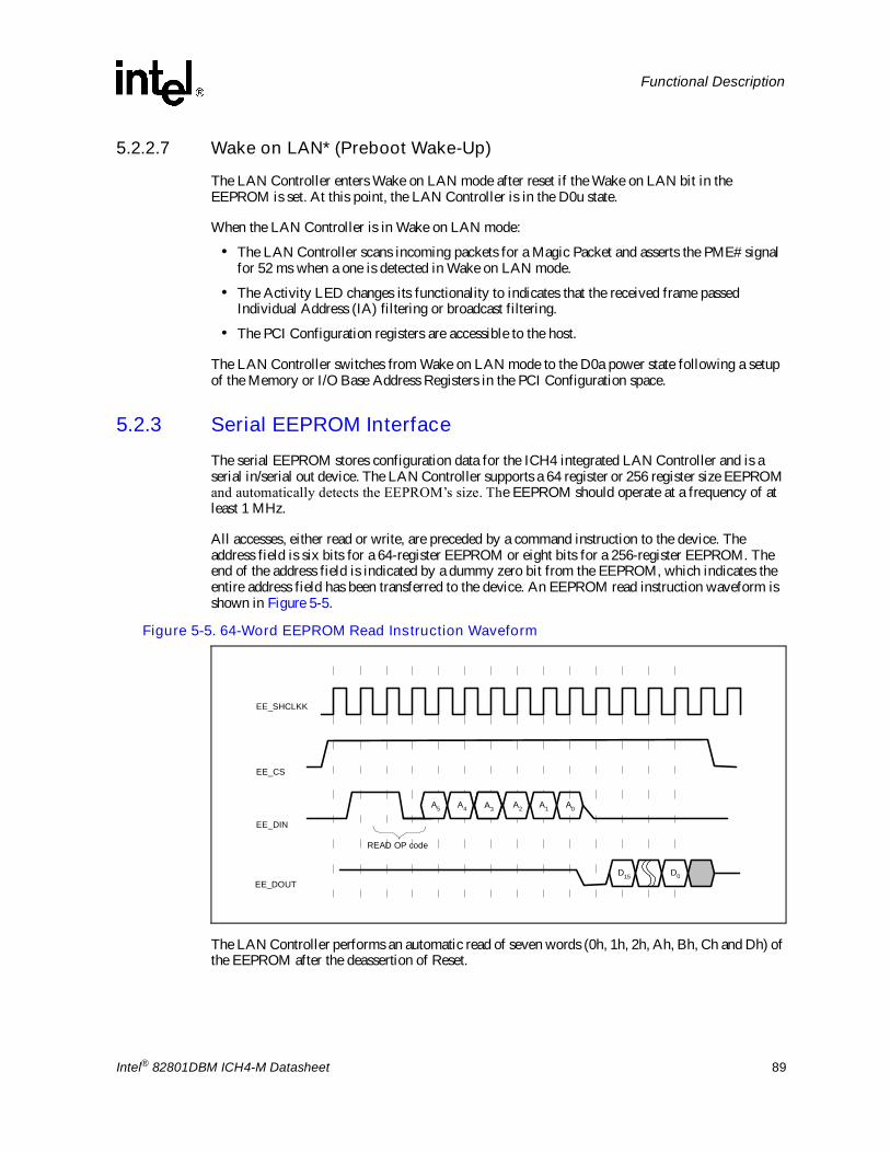
Intel® 82801DBM ICH4-M Datasheet 89
Functional Description
5.2.2.7 Wake on LAN* (Preboot Wake-Up)
The LAN Controller enters Wake on LAN mode after reset if the Wake on LAN bit in the EEPROM is set. At this point, the LAN Controller is in the D0u state.
When the LAN Controller is in Wake on LAN mode:
� The LAN Controller scans incoming packets for a Magic Packet and asserts the PME# signal for 52 ms when a one is detected in Wake on LAN mode.
� The Activity LED changes its functionality to indicates that the received frame passed Individual Address (IA) filtering or broadcast filtering.
� The PCI Configuration registers are accessible to the host.
The LAN Controller switches from Wake on LAN mode to the D0a power state following a setup of the Memory or I/O Base Address Registers in the PCI Configuration space.
5.2.3 Serial EEPROM InterfaceThe serial EEPROM stores configuration data for the ICH4 integrated LAN Controller and is a serial in/serial out device. The LAN Controller supports a 64 register or 256 register size EEPROM and automatically detects the EEPROM�s size. The EEPROM should operate at a frequency of at least 1 MHz.
All accesses, either read or write, are preceded by a command instruction to the device. The address field is six bits for a 64-register EEPROM or eight bits for a 256-register EEPROM. The end of the address field is indicated by a dummy zero bit from the EEPROM, which indicates the entire address field has been transferred to the device. An EEPROM read instruction waveform is shown in Figure 5-5.
The LAN Controller performs an automatic read of seven words (0h, 1h, 2h, Ah, Bh, Ch and Dh) of the EEPROM after the deassertion of Reset.
Figure 5-5. 64-Word EEPROM Read Instruction Waveform
A1A0
EE_CS
EE_SHCLKK
EE_DIN
EE_DOUT
A5 A4 A2
D15 D0
READ OP code
A3 A1 A0

90 Intel® 82801DBM ICH4-M Datasheet
Functional Description
5.2.4 CSMA/CD UnitThe ICH4 integrated LAN Controller CSMA/CD unit implements both the IEEE 802.3 Ethernet 10 Mbps and IEEE 802.3u Fast Ethernet 100 Mbps standards. It performs all the CSMA/CD protocol functions (e.g., transmission, reception, collision handling, etc.). The LAN Controller CSMA/CD unit interfaces to the 82562ET/EM 10/100 Mbps Ethernet through the ICH4�s LAN Connect interface signals.
5.2.4.1 Full Duplex
When operating in full-duplex mode, the LAN Controller can transmit and receive frames simultaneously. Transmission starts regardless of the state of the internal receive path. Reception starts when the LAN Connect component detects a valid frame on its receive differential pair. The ICH4 integrated LAN Controller also supports the IEEE 802.3x flow control standard, when in full-duplex mode.
The LAN Controller operates in either half-duplex mode or full-duplex mode. For proper operation, both the LAN Controller CSMA/CD module and the discrete LAN Connect component must be set to the same duplex mode. The CSMA duplex mode is set by the LAN Controller Configure command or forced by automatically tracking the mode in the LAN Connect component. Following reset, the CSMA defaults to automatically track the LAN Connect component duplex mode.
The selection of duplex operation (full or half) and flow control is done in two levels: MAC and LAN Connect.
5.2.4.2 Flow Control
The LAN Controller supports IEEE 802.3x frame-based flow control frames only in both full duplex and half duplex switched environments. The LAN Controller flow control feature is not intended to be used in shared media environments.
Flow control is optional in full-duplex mode and is selected through software configuration. There are three modes of flow control that can be selected: frame-based transmit flow control, frame-based receive flow control, and none.
5.2.4.3 Address Filtering Modifications
The LAN Controller can be configured to ignore one bit when checking for its Individual Address (IA) on incoming receive frames. The address bit, known as the Upper/Lower (U/L) bit, is the second least significant bit of the first byte of the IA. This bit may be used, in some cases, as a priority indication bit. When configured to do so, the LAN Controller passes any frame that matches all other 47 address bits of its IA, regardless of the U/L bit value.
This configuration only affects the LAN Controller specific IA and not multicast, multi-IA, or broadcast address filtering. The LAN Controller does not attribute any priority to frames with this bit set, it simply passes them to memory regardless of this bit.

Intel® 82801DBM ICH4-M Datasheet 91
Functional Description
5.2.4.4 VLAN Support
The LAN Controller supports the IEEE 802.1 standard VLAN. All VLAN flows will be implemented by software. The LAN Controller supports the reception of long frames, specifically frames longer than 1518 bytes, including the CRC, if software sets the Long Receive OK bit in the Configuration command. Otherwise, �long� frames are discarded.
5.2.5 Media Management InterfaceThe management interface allows the processor to control the LAN Connect component via a control register in the ICH4 integrated LAN Controller. This allows the software driver to place the LAN Connect in specific modes (e.g., full duplex, loopback, power down, etc.) without the need for specific hardware pins to select the desired mode. This structure allows the LAN Controller to query the LAN Connect component for status of the link. This register is the MDI Control Register and resides at offset 10h in the LAN Controller CSR. The MDI registers reside within the LAN Connect component, and are described in detail in the LAN Connect component�s datasheet. The processor writes commands to this register and the LAN Controller reads or writes the control/status parameters to the LAN Connect component through the MDI register.
5.2.6 TCO FunctionalityThe ICH4 integrated LAN controller supports management communication to reduce Total Cost of Ownership (TCO). It has a System Management Bus (SMB) on which the LAN controller is a slave device. The SMB is used as an interface between the LAN controller and the integrated host controller. An EEPROM of 256 words is required to support the heartbeat command.
5.2.6.1 Receive Functionality
In the power-up state, the LAN controller transfers TCO packets to the host as any other packet. These packets include a new status indication bit in the Receive Frame Descriptor (RFD) status register and have a specific port number indicating TCO packet recognition. In the power-down state, the TCO packets are treated as wake-up packets. The ICH4 integrated LAN controller asserts the PME# signal and delivers the first 120 bytes of the packet to the host.
5.2.6.2 Transmit Functionality
The ICH4 integrated LAN controller supports the Heartbeat (HB) transmission command from the SMB interface. The send HB packet command includes a system health status issued by the integrated system controller. The LAN controller computes a matched checksum and CRC and will transmit the HB packet from its serial EEPROM. The HB packet size and structure are not limited as long as it fits within the EEPROM size. In this case, the EEPROM size is 256 words to enable the storage of the HB packet (the first 64 words are used for driver specific data).
Note: On the SMB, the send heartbeat packet command is not normally used in the D0 power state. The one exception in which it is used in the D0 state is when the system is hung. In normal operating mode, the heartbeat packets are transmitted through the ICH4 integrated LAN controller software similar to other packets.

92 Intel® 82801DBM ICH4-M Datasheet
Functional Description
5.3 LPC Bridge (with System and Management Functions) (D31:F0)The LPC Bridge function of the ICH4 resides in PCI Device 31:Function 0. In addition to the LPC bridge function, D31:F0 contains other functional units including DMA, Interrupt Controllers, Timers, Power Management, System Management, GPIO, and RTC. In this chapter, registers and functions associated with other functional units (power management, GPIO, USB, IDE, etc.) are described in their respective sections.
5.3.1 LPC InterfaceThe ICH4 implements an LPC interface as described in the LPC 1.0 specification. The LPC interface to the ICH4 is shown in Figure 5-6. Note that the ICH4 implements all of the signals that are shown as optional, but peripherals are not required to do so.
Figure 5-6. LPC Interface Diagram
LAD[3:0]
ICH4
Super I/O
LSMI#(optional)
LPCPD#(optional)
LDRQ#(optional)
LFRAME#
PCICLK
PCIRST#
PCISERIRQ
PCIPME#
PCI Bus
SUS_STAT#
GPI
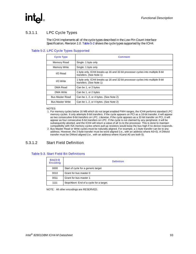
Intel® 82801DBM ICH4-M Datasheet 93
Functional Description
5.3.1.1 LPC Cycle Types
The ICH4 implements all of the cycle types described in the Low Pin Count Interface Specification, Revision 1.0. Table 5-2 shows the cycle types supported by the ICH4.
NOTES:1. For memory cycles below 16 MB which do not target enabled FWH ranges, the ICH4 performs standard LPC
memory cycles. It only attempts 8-bit transfers. If the cycle appears on PCI as a 16-bit transfer, it will appear as two consecutive 8-bit transfers on LPC. Likewise, if the cycle appears as a 32-bit transfer on PCI, it will appear as four consecutive 8-bit transfers on LPC. If the cycle is not claimed by any peripheral, it will be subsequently aborted, and the ICH4 will return a value of all 1s to the processor. This is done to maintain compatibility with ISA memory cycles where pull-up resistors would keep the bus high if no device responds.
2. Bus Master Read or Write cycles must be naturally aligned. For example, a 1-byte transfer can be to any address. However, the 2-byte transfer must be word aligned (i.e., with an address where A0=0). A DWord transfer must be DWord aligned (i.e., with an address where A1and A0 are both 0).
5.3.1.2 Start Field Definition
NOTE: All other encodings are RESERVED.
Table 5-2. LPC Cycle Types Supported
Cycle Type Comment
Memory Read Single: 1 byte only
Memory Write Single: 1 byte only
I/O Read 1 byte only. ICH4 breaks up 16 and 32-bit processor cycles into multiple 8-bit transfers. (See Note 1)
I/O Write 1 byte only. ICH4 breaks up 16 and 32-bit processor cycles into multiple 8-bit transfers. (See Note 1)
DMA Read Can be 1, or 2 bytes
DMA Write Can be 1, or 2 bytes
Bus Master Read Can be 1, 2, or 4 bytes. (See Note 2)
Bus Master Write Can be 1, 2, or 4 bytes. (See Note 2)
Table 5-3. Start Field Bit Definitions
Bits[3:0]Encoding Definition
0000 Start of cycle for a generic target
0010 Grant for bus master 0
0011 Grant for bus master 1
1111 Stop/Abort: End of a cycle for a target.

94 Intel® 82801DBM ICH4-M Datasheet
Functional Description
5.3.1.3 Cycle Type / Direction (CYCTYPE + DIR)
The ICH4 will always drive bit 0 of this field to 0. Peripherals running bus master cycles must also drive bit 0 to 0. Table 5-4 shows the valid bit encodings:
5.3.1.4 SizeBits[3:2] are reserved. The ICH4 always drives them to 00. Peripherals running bus master cycles are also supposed to drive 00 for bits 3:2, however, the ICH4 will ignore those bits. Bits[1:0] are encoded as shown in Table 5-5.
5.3.1.5 SYNCValid values for the SYNC field are provided in Table 5-6.
NOTE: All other combinations are RESERVED.
Table 5-4. Cycle Type Bit Definitions
Bits[3:2] Bit[1] Definition
00 0 I/O Read
00 1 I/O Write
01 0 Memory Read
01 1 Memory Write
10 0 DMA Read
10 1 DMA Write
11 x Reserved. If a peripheral performing a bus master cycle generates this value, the ICH4 will abort the cycle.
Table 5-5. Transfer Size Bit Definition
Bits[1:0] Size
00 8-bit transfer (1 byte)
01 16-bit transfer (2 bytes)
10 Reserved. The ICH4 will never drive this combination. If a peripheral running a bus master cycle drives this combination, the ICH4 may abort the transfer.
11 32-bit transfer (4 bytes)
Table 5-6. SYNC Bit Definition
Bits[3:0] Indication
0000 Ready: SYNC achieved with no error. For DMA transfers, this also indicates DMA request deassertion and no more transfers desired for that channel.
0101 Short Wait: Part indicating wait-states. For bus master cycles, the ICH4 will not use this encoding. It will instead use the Long Wait encoding (see next encoding below).
0110 Long Wait: Part indicating wait-states, and many wait-states will be added. This encoding driven by the ICH4 for bus master cycles, rather than the Short Wait (0101).
1001Ready More (Used only by peripheral for DMA cycle): SYNC achieved with no error and more DMA transfers desired to continue after this transfer. This value is valid only on DMA transfers and is not allowed for any other type of cycle.
1010Error: Sync achieved with error. This is generally used to replace the SERR# or IOCHK# signal on the PCI/ISA bus. It indicates that the data is to be transferred, but there is a serious error in this transfer. For DMA transfers, this not only indicates an error, but also indicates DMA request deassertion and no more transfers desired for that channel.

Intel® 82801DBM ICH4-M Datasheet 95
Functional Description
5.3.1.6 SYNC Time-Out
There are several error cases that can occur on the LPC interface. Table 5-7 indicates the failing case and the ICH4 response.
There may be other peripheral failure conditions, however these are not handled by the ICH4.
5.3.1.7 SYNC Error Indication
The SYNC protocol allows the peripheral to report an error via the LAD[3:0] = 1010b encoding. The intent of this encoding is to give peripherals a method of communicating errors to aid higher layers with more robust error recovery.
If the ICH4 was reading data from a peripheral, data will still be transferred in the next two nibbles. This data may be invalid, but it must be transferred by the peripheral. If the ICH4 was writing data to the peripheral, the data had already been transferred.
In the case of multiple byte cycles (e.g., as for memory and DMA cycles) an error SYNC terminates the cycle. Therefore, if the ICH4 is transferring 4 bytes from a device and the device returns the error SYNC in the first byte, the other three bytes will not be transferred.
Upon recognizing the SYNC field indicating an error, the ICH4 will treat this the same as IOCHK# going active on the ISA bus.
Table 5-7. Intel® ICH4 Response to Sync Failures
Possible Sync Failure ICH4 Response
ICH4 starts a Memory, I/O, or DMA cycle, but no device drives a valid SYNC after 4 consecutive clocks. This could occur if the processor tries to access an I/O location to which no device is mapped.
ICH4 aborts the cycle after the fourth clock.
ICH4 drives a Memory, I/O, or DMA cycle, and a peripheral drives more than 8 consecutive valid SYNC to insert wait-states using the Short (0101b�) encoding for SYNC. This could occur if the peripheral is not operating properly.
Continues waiting
ICH4 starts a Memory, I/O, or DMA cycle, and a peripheral drives an invalid SYNC pattern. This could occur if the peripheral is not operating properly or if there is excessive noise on the LPC interface.
ICH4 aborts the cycle when the invalid Sync is recognized.

96 Intel® 82801DBM ICH4-M Datasheet
Functional Description
5.3.1.8 LFRAME# Usage
Start of Cycle
For Memory, I/O, and DMA cycles, the ICH4 asserts LFRAME# for 1 clock at the beginning of the cycle (Figure 5-7). During that clock, the ICH4 drives LAD[3:0] with the proper START field.
Abort Mechanism
When performing an Abort, the ICH4 drives LFRAME# active for four consecutive clocks. On the fourth clock, it drives LAD[3:0] to 1111b.
The ICH4 performs an abort for the following cases (possible failure cases):
� ICH4 starts a Memory, I/O, or DMA cycle, but no device drives a valid SYNC after four consecutive clocks.
� ICH4 starts a Memory, I/O, or DMA cycle, and the peripheral drives an invalid SYNC pattern.
� A peripheral drives an illegal address when performing bus master cycles.
� A peripheral drives an invalid value.
Figure 5-7. Typical Timing for LFRAME#
LFRAME#
Start
LCLK
LAD[3:0]CYCTYPE
ADDR Start
Dir & Size
TAR Sync Data TAR1 - 8
Clocks2
Clocks1 - n
Clocks2
Clocks2
Clocks1
Clock1
Clock
Figure 5-8. Abort Mechanism
LFRAME#
Start
LCLK
LAD[3:0]CYCTYPE
ADDR
Dir & Size
TAR Sync Peripheral muststop driving
Too manySyncs causes
timeout
Chipset willdrive high

Intel® 82801DBM ICH4-M Datasheet 97
Functional Description
5.3.1.9 I/O Cycles
For I/O cycles targeting registers specified in the ICH4�s decode ranges, the ICH4 performs I/O cycles as defined in the LPC specification. These will be 8-bit transfers. If the processor attempts a 16-bit or 32-bit transfer, the ICH4 breaks the cycle up into multiple 8-bit transfers to consecutive I/O addresses.
Note: If the cycle is not claimed by any peripheral (and subsequently aborted), the ICH4 returns a value of all 1s (FFh) to the processor. This is to maintain compatibility with ISA I/O cycles where pull-up resistors would keep the bus high if no device responds.
5.3.1.10 Bus Master Cycles
The ICH4 supports Bus Master cycles and requests (using LDRQ#) as defined in the LPC specification. The ICH4 has two LDRQ# inputs, and thus, supports two separate bus master devices. It uses the associated START fields for Bus Master 0 (0010b) or Bus Master 1 (0011b).
Note: The ICH4 does not support LPC Bus Masters performing I/O cycles. LPC Bus Masters should only perform memory read or memory write cycles.
5.3.1.11 LPC Power Management
CLKRUN# Protocol
The CLKRUN# protocol is same as the PCI specification. Stopping the PCI clock stops the LPC clock.
LPCPD# Protocol
Same timings as for SUS_STAT#. Upon driving SUS_STAT# low, LPC peripherals will drive LDRQ# low or tri-state it. ICH4 will shut off the LDRQ# input buffers. After driving SUS_STAT# active, the ICH4 drives LFRAME# low, and tri-states (or drive low) LAD[3:0].
Note: The LPC specification defines he LPCPD# protocol where there is at least 30 us from LPCPD# assertion to LRST# assertion. This specification explicitly states that this protocol only applies to entry/exit of low power states (which does not include asynchronous reset events). The ICH4 will assert the SUS_STAT# (connects to LPCPD#) and PCIRST# connects to LRST#) at the same time when the core logic is reset (via CF9, PWROK, SYS_RESET#, etc.). This is not inconsistent with LPC LPCPD# protocol.
5.3.1.12 Configuration and ICH4 Implications
LPC Interface Decoders
To allow the I/O cycles and memory mapped cycles to go to the LPC interface, the ICH4 includes several decoders. During configuration, the ICH4 must be programmed with the same decode ranges as the peripheral. The decoders are programmed via the Device 31:Function 0 configuration space.
Note: The ICH4 cannot accept PCI write cycles from PCI-to-PCI bridges or devices with similar characteristics (specifically those with a �Retry Read� feature which is enabled) to an LPC device if there is an outstanding LPC read cycle towards the same PCI device or bridge. These cycles are
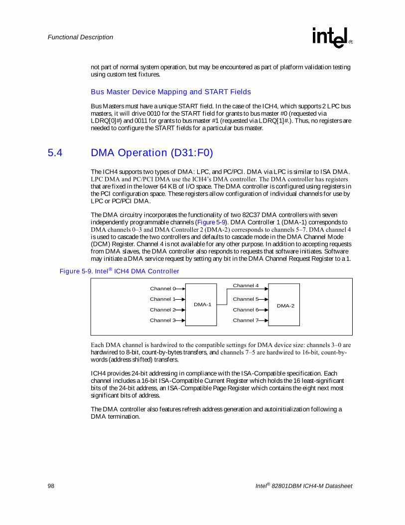
98 Intel® 82801DBM ICH4-M Datasheet
Functional Description
not part of normal system operation, but may be encountered as part of platform validation testing using custom test fixtures.
Bus Master Device Mapping and START Fields
Bus Masters must have a unique START field. In the case of the ICH4, which supports 2 LPC bus masters, it will drive 0010 for the START field for grants to bus master #0 (requested via LDRQ[0]#) and 0011 for grants to bus master #1 (requested via LDRQ[1]#.). Thus, no registers are needed to configure the START fields for a particular bus master.
5.4 DMA Operation (D31:F0)The ICH4 supports two types of DMA: LPC, and PC/PCI. DMA via LPC is similar to ISA DMA. LPC DMA and PC/PCI DMA use the ICH4�s DMA controller. The DMA controller has registers that are fixed in the lower 64 KB of I/O space. The DMA controller is configured using registers in the PCI configuration space. These registers allow configuration of individual channels for use by LPC or PC/PCI DMA.
The DMA circuitry incorporates the functionality of two 82C37 DMA controllers with seven independently programmable channels (Figure 5-9). DMA Controller 1 (DMA-1) corresponds to DMA channels 0�3 and DMA Controller 2 (DMA-2) corresponds to channels 5�7. DMA channel 4 is used to cascade the two controllers and defaults to cascade mode in the DMA Channel Mode (DCM) Register. Channel 4 is not available for any other purpose. In addition to accepting requests from DMA slaves, the DMA controller also responds to requests that software initiates. Software may initiate a DMA service request by setting any bit in the DMA Channel Request Register to a 1.
Each DMA channel is hardwired to the compatible settings for DMA device size: channels 3�0 are hardwired to 8-bit, count-by-bytes transfers, and channels 7�5 are hardwired to 16-bit, count-by-words (address shifted) transfers.
ICH4 provides 24-bit addressing in compliance with the ISA-Compatible specification. Each channel includes a 16-bit ISA-Compatible Current Register which holds the 16 least-significant bits of the 24-bit address, an ISA-Compatible Page Register which contains the eight next most significant bits of address.
The DMA controller also features refresh address generation and autoinitialization following a DMA termination.
Figure 5-9. Intel® ICH4 DMA Controller
Channel 0
Channel 1
Channel 2
Channel 3
Channel 4
Channel 5
Channel 6
Channel 7
DMA-1 DMA-2

Intel® 82801DBM ICH4-M Datasheet 99
Functional Description
5.4.1 Channel PriorityFor priority resolution, the DMA consists of two logical channel groups: channels 0�3 and channels 4�7. Each group may be in either fixed or rotate mode, as determined by the DMA Command Register.
DMA I/O slaves normally assert their DREQ line to arbitrate for DMA service. However, a software request for DMA service can be presented through each channel's DMA Request Register. A software request is subject to the same prioritization as any hardware request. See the detailed register description for Request Register programming information in Section 9.2.
5.4.1.1 Fixed Priority
The initial fixed priority structure is as follows:
The fixed priority ordering is 0, 1, 2, 3, 5, 6, and 7. In this scheme, channel 0 has the highest priority, and channel 7 has the lowest priority. Channels 3�0 of DMA-1 assume the priority position of channel 4 in DMA-2, thus taking priority over channels 5, 6, and 7.
5.4.1.2 Rotating Priority
Rotation allows for "fairness" in priority resolution. The priority chain rotates so that the last channel serviced is assigned the lowest priority in the channel group (0�3, 5�7).
Channels 0�3 rotate as a group of 4. They are always placed between channel 5 and channel 7 in the priority list.
Channel 5�7 rotate as part of a group of 4. That is, channels 5�7 form the first three positions in the rotation, while channel group 0�3 comprises the fourth position in the arbitration.
5.4.2 Address Compatibility ModeWhen the DMA is operating, the addresses do not increment or decrement through the High and Low Page Registers. Therefore, if a 24-bit address is 01FFFFh and increments, the next address will be 010000h, not 020000h. Similarly, if a 24-bit address is 020000h and decrements, the next address will be 02FFFFh, not 01FFFFh. However, when the DMA is operating in 16-bit mode, the addresses still do not increment or decrement through the High and Low Page Registers but the page boundary is now 128 kB. Therefore, if a 24 bit address is 01FFFEh and increments, the next address will be 000000h, not 010000h. Similarly, if a 24 bit address is 020000h and decrements, the next address will be 03FFFEh, not 02FFFEh. This is compatible with the 82C37 and Page Register implementation used in the PC-AT. This mode is set after CPURST is valid.
High priority.....Low priority
(0, 1, 2, 3) (5, 6, 7)

100 Intel® 82801DBM ICH4-M Datasheet
Functional Description
5.4.3 Summary of DMA Transfer SizesTable 5-8 lists each of the DMA device transfer sizes. The column labeled �Current Byte/Word Count Register� indicates that the register contents represents either the number of bytes to transfer or the number of 16-bit words to transfer. The column labeled �Current Address Increment/Decrement� indicates the number added to or taken from the Current Address register after each DMA transfer cycle. The DMA Channel Mode Register determines if the Current Address Register will be incremented or decremented.
5.4.3.1 Address Shifting When Programmed for 16-Bit I/O Count by Words
The ICH4 maintains compatibility with the implementation of the DMA in the PC AT which used the 82C37. The DMA shifts the addresses for transfers to/from a 16-bit device count-by-words. Note that the least significant bit of the Low Page Register is dropped in 16-bit shifted mode. When programming the Current Address Register (when the DMA channel is in this mode), the Current Address must be programmed to an even address with the address value shifted right by one bit. The address shifting is shown in Table 5-9.
NOTE: The least significant bit of the Page Register is dropped in 16-bit shifted mode.
5.4.4 AutoinitializeBy programming a bit in the DMA Channel Mode Register, a channel may be set up as an autoinitialize channel. When a channel undergoes autoinitialization, the original values of the Current Page, Current Address, and Current Byte/Word Count registers are automatically restored from the Base Page, Address, and Byte/Word Count Registers of that channel following TC. The Base registers are loaded simultaneously with the Current registers by the microprocessor when the DMA channel is programmed and remain unchanged throughout the DMA service. The mask bit is not set when the channel is in autoinitialize. Following autoinitialize, the channel is ready to perform another DMA service, without processor intervention, as soon as a valid DREQ is detected.
Table 5-8. DMA Transfer Size
DMA Device Date Size And Word Count Current Byte/Word Count Register
Current Address Increment/Decrement
8-Bit I/O, Count By Bytes Bytes 1
16-Bit I/O, Count By Words (Address Shifted) Words 1
Table 5-9. Address Shifting in 16-bit I/O DMA Transfers
OutputAddress
8-Bit I/O Programmed Address (Ch 0�3)
16-Bit I/O Programmed Address (Ch 5�7)(Shifted)
A0A[16:1]A[23:17]
A0A[16:1]A[23:17]
0A[15:0]
A[23:17]

Intel® 82801DBM ICH4-M Datasheet 101
Functional Description
5.4.5 Software CommandsThere are three additional special software commands that the DMA controller can execute. The three software commands are:
� Clear Byte Pointer Flip-Flop
� Master Clear
� Clear Mask Register
They do not depend on any specific bit pattern on the data bus.
5.4.5.1 Clear Byte Pointer Flip-Flop
This command is executed prior to writing or reading new address or word count information to/from the DMA controller. This initializes the flip-flop to a known state so that subsequent accesses to register contents by the microprocessor will address upper and lower bytes in the correct sequence.
When the host processor is reading or writing DMA registers, two Byte Pointer flip-flops are used; one for channels 0�3 and one for channels 4�7. Both of these act independently. There are separate software commands for clearing each of them (0Ch for channels 0�3, 0D8h for channels 4�7).
5.4.5.2 DMA Master Clear
This software instruction has the same effect as the hardware reset. The Command, Status, Request, and Internal First/Last Flip-Flop registers are cleared and the Mask register is set. The DMA controller will enter the idle cycle.
There are two independent master clear commands; 0Dh which acts on channels 0�3, and 0DAh which acts on channels 4�7.
5.4.5.3 Clear Mask Register
This command clears the mask bits of all four channels, enabling them to accept DMA requests. I/O port 00Eh is used for channels 0�3 and I/O port 0DCh is used for channels 4�7.
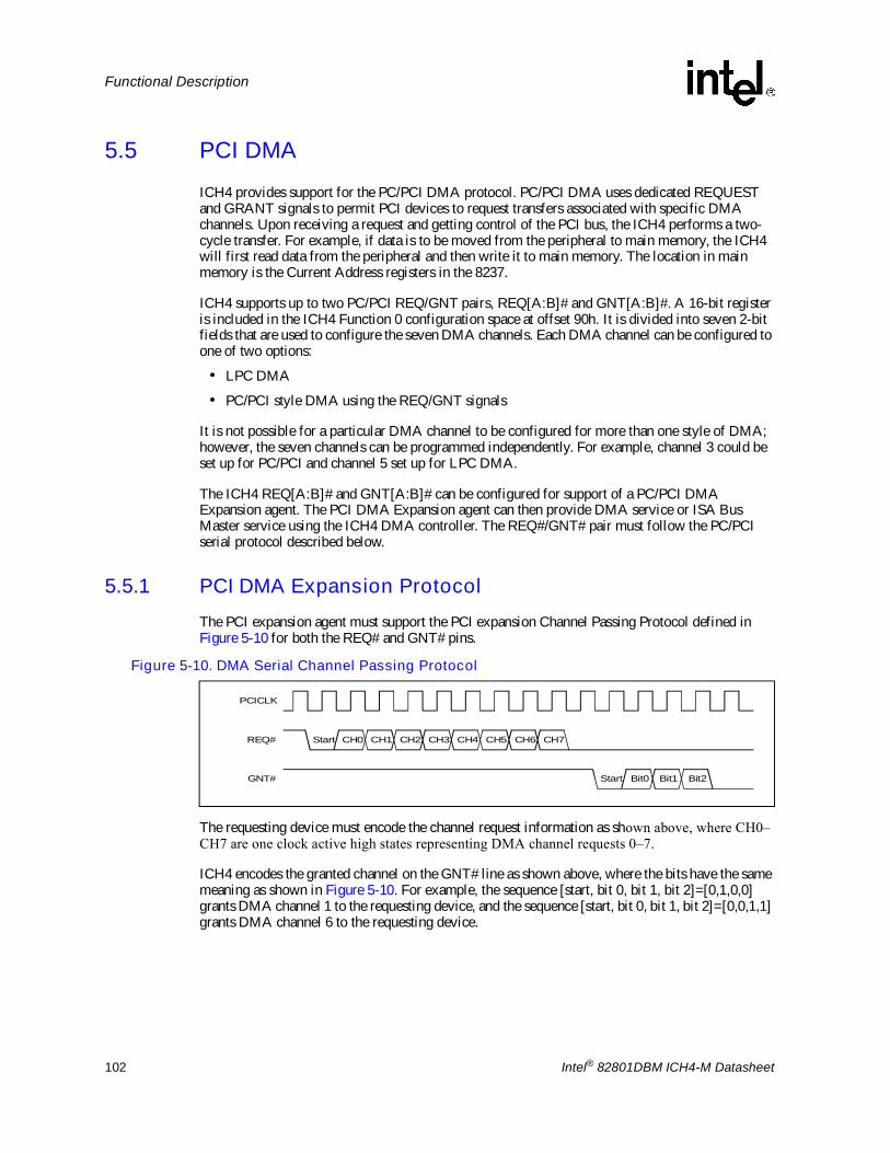
102 Intel® 82801DBM ICH4-M Datasheet
Functional Description
5.5 PCI DMAICH4 provides support for the PC/PCI DMA protocol. PC/PCI DMA uses dedicated REQUEST and GRANT signals to permit PCI devices to request transfers associated with specific DMA channels. Upon receiving a request and getting control of the PCI bus, the ICH4 performs a two-cycle transfer. For example, if data is to be moved from the peripheral to main memory, the ICH4 will first read data from the peripheral and then write it to main memory. The location in main memory is the Current Address registers in the 8237.
ICH4 supports up to two PC/PCI REQ/GNT pairs, REQ[A:B]# and GNT[A:B]#. A 16-bit register is included in the ICH4 Function 0 configuration space at offset 90h. It is divided into seven 2-bit fields that are used to configure the seven DMA channels. Each DMA channel can be configured to one of two options:
� LPC DMA
� PC/PCI style DMA using the REQ/GNT signals
It is not possible for a particular DMA channel to be configured for more than one style of DMA; however, the seven channels can be programmed independently. For example, channel 3 could be set up for PC/PCI and channel 5 set up for LPC DMA.
The ICH4 REQ[A:B]# and GNT[A:B]# can be configured for support of a PC/PCI DMA Expansion agent. The PCI DMA Expansion agent can then provide DMA service or ISA Bus Master service using the ICH4 DMA controller. The REQ#/GNT# pair must follow the PC/PCI serial protocol described below.
5.5.1 PCI DMA Expansion Protocol The PCI expansion agent must support the PCI expansion Channel Passing Protocol defined in Figure 5-10 for both the REQ# and GNT# pins.
The requesting device must encode the channel request information as shown above, where CH0�CH7 are one clock active high states representing DMA channel requests 0�7.
ICH4 encodes the granted channel on the GNT# line as shown above, where the bits have the same meaning as shown in Figure 5-10. For example, the sequence [start, bit 0, bit 1, bit 2]=[0,1,0,0] grants DMA channel 1 to the requesting device, and the sequence [start, bit 0, bit 1, bit 2]=[0,0,1,1] grants DMA channel 6 to the requesting device.
Figure 5-10. DMA Serial Channel Passing Protocol
PCICLK
Start CH0 CH1 CH2 CH3 CH4 CH5 CH6 CH7
Bit0 Bit1 Bit2Start
REQ#
GNT#

Intel® 82801DBM ICH4-M Datasheet 103
Functional Description
All PCI DMA expansion agents must use the channel passing protocol described above. They must also work as follows:
� If a PCI DMA expansion agent has more than one request active, it must resend the request serial protocol after one of the requests has been granted the bus and it has completed its transfer. The expansion device should drive its REQ# inactive for two clocks and then transmit the serial channel passing protocol again, even if there are no new requests from the PCI expansion agent to ICH4. For example: If a PCI expansion agent had active requests for DMA channel 1 and channel 5, it would pass this information to ICH4 through the expansion channel passing protocol. If after receiving GNT# (assume for CH5) and having the device finish its transfer (device stops driving request to PCI expansion agent) it would then need to re-transmit the expansion channel passing protocol to inform ICH4 that DMA channel 1 was still requesting the bus, even if that was the only request the expansion device had pending.
� If a PCI DMA expansion agent has a request go inactive before ICH4 asserts GNT#, it must resend the expansion channel passing protocol to update ICH4 with this new request information. For example: If a PCI expansion agent has DMA channel 1 and 2 requests pending it will send them serially to ICH4 using the expansion channel passing protocol. If, however, DMA channel 1 goes inactive into the expansion agent before the expansion agent receives a GNT# from ICH4, the expansion agent MUST pull its REQ# line high for ONE clock and resend the expansion channel passing information with only DMA channel 2 active. Note that ICH4 does not do anything special to catch this case because a DREQ going inactive before a DACK# is received is not allowed in the ISA DMA protocol and, therefore, does not need to work properly in this protocol either. This requirement is needed to be able to support Plug-n-Play ISA devices that toggle DREQ# lines to determine if those lines are free in the system.
� If a PCI expansion agent has sent its serial request information and receives a new DMA request before receiving GNT#, the agent must resend the serial request with the new request active. For example: If a PCI expansion agent has already passed requests for DMA channel 1 and 2 and sees DREQ 3 active before a GNT is received, the device must pull its REQ# line high for one clock and resend the expansion channel passing information with all three channels active.
The three cases above require the following functionality in the PCI DMA expansion device:
� Drive REQ# inactive for one clock to signal new request information.
� Drive REQ# inactive for two clocks to signal that a request that had been granted the bus has gone inactive.
� The REQ# and GNT# state machines must run independently and concurrently (i.e., a GNT# could be received while in the middle of sending a serial REQ# or a GNT# could be active while REQ# is inactive).
5.5.2 PCI DMA Expansion CyclesICH4�s support of the PC/PCI DMA Protocol currently consists of four types of cycles: Memory to I/O, I/O to Memory, Verify, and ISA Master cycles. ISA Masters are supported through the use of a DMA channel that has been programmed for cascade mode.
The DMA controller does a two cycle transfer (a load followed by a store) as opposed to the ISA "fly-by" cycle for PC/PCI DMA agents. The memory portion of the cycle generates a PCI memory read or memory write bus cycle, its address representing the selected memory.

104 Intel® 82801DBM ICH4-M Datasheet
Functional Description
The I/O portion of the DMA cycle generates a PCI I/O cycle to one of four I/O addresses (Table 5-10). Note that these cycles must be qualified by an active GNT# signal to the requesting device.
5.5.3 DMA AddressesThe memory portion of the cycle generates a PCI memory read or memory write bus cycle (its address representing the selected memory). The I/O portion of the DMA cycle generates a PCI I/O cycle to one of the four I/O addresses listed in Table 5-10.
5.5.4 DMA Data GenerationThe data generated by PC/PCI devices on I/O reads when they have an active GNT# is on the lower two bytes of the PCI AD bus. Table 5-11 lists the PCI pins that the data appears on for 8-bit and 16-bit channels. Each I/O read results in one memory write, and each memory read results in one I/O write. If the I/O device is 8 bit, the ICH4 performs an 8-bit memory write. The ICH4 does not assemble the I/O read into a DWord for writing to memory. Similarly, the ICH4 does not disassemble a DWord read from memory to the I/O device.
5.5.5 DMA Byte Enable GenerationThe byte enables generated by the ICH4 on I/O reads and writes must correspond to the size of the I/O device. Table 5-12 defines the byte enables asserted for 8-bit and 16-bit DMA cycles.
NOTE: For verify cycles the value of the Byte Enables (BEs) is a �don�t care�.
Table 5-10. DMA Cycle vs. I/O Address
DMA Cycle Type DMA I/O Address PCI Cycle Type
Normal 00h I/O Read/Write
Normal TC 04h I/O Read/Write
Verify 0C0h I/O Read
Verify TC 0C4h I/O Read
Table 5-11. PCI Data Bus vs. DMA I/O Port Size
PCI DMA I/O Port Size PCI Data Bus Connection
Byte AD[7:0]
Word AD[15:0]
Table 5-12. DMA I/O Cycle Width vs. BE[3:0]#
BE[3:0]# Description
1110b 8-bit DMA I/O Cycle: Channels 0-3
1100b 16-bit DMA I/O Cycle: Channels 5-7

Intel® 82801DBM ICH4-M Datasheet 105
Functional Description
5.5.6 DMA Cycle TerminationDMA cycles are terminated when a terminal count is reached in the DMA controller and the channel is not in autoinitialize mode, or when the PC/PCI device deasserts its request. The PC/PCI device must follow explicit rules when deasserting its request, or the ICH4 may not see it in time and run an extra I/O and memory cycle.
The PC/PCI device must deassert its request 7 PCICLKs before it generates TRDY# on the I/O read or write cycle, or the ICH4 is allowed to generate another DMA cycle. For transfers to memory, this means that the memory portion of the cycle is run without an asserted PC/PCI REQ#.
5.5.7 LPC DMADMA on LPC is handled through the use of the LDRQ# lines from peripherals and special encodings on LAD[3:0] from the host. Single, Demand, Verify, and Increment modes are supported on the LPC interface. Channels 0�3 are 8 bit channels. Channels 5�7 are 16-bit channels. Channel 4 is reserved as a generic bus master request.
5.5.8 Asserting DMA RequestsPeripherals that need DMA service encode their requested channel number on the LDRQ# signal. To simplify the protocol, each peripheral on the LPC interface has its own dedicated LDRQ# signal (they may not be shared between two separate peripherals). The ICH4 has two LDRQ# inputs, allowing at least two devices to support DMA or bus mastering.
LDRQ# is synchronous with LCLK (PCI clock). As shown in Figure 5-11 the peripheral uses the following serial encoding sequence:
� Peripheral starts the sequence by asserting LDRQ# low (start bit). LDRQ# is high during idle conditions.
� The next 3 bits contain the encoded DMA channel number (MSB first).
� The next bit (ACT) indicates whether the request for the indicated DMA channel is active or inactive. The ACT bit will be a 1(high) to indicate if it is active and 0 (low) if it is inactive. The case where ACT is low is rare, and is only used to indicate that a previous request for that channel is being abandoned.
� After the active/inactive indication, the LDRQ# signal must go high for at least 1 clock. After that one clock, LDRQ# signal can be brought low to the next encoding sequence.
If another DMA channel also needs to request a transfer, another sequence can be sent on LDRQ#. For example, if an encoded request is sent for channel 2 and then channel 3 needs a transfer before the cycle for channel 2 is run on the interface, the peripheral can send the encoded request for channel 3. This allows multiple DMA agents behind an I/O device to request use of the LPC interface and the I/O device does not need to self-arbitrate before sending the message.
Figure 5-11. DMA Request Assertion Through LDRQ#
Start MSB LSB ACT Start
LCLK
LDRQ#

106 Intel® 82801DBM ICH4-M Datasheet
Functional Description
5.5.9 Abandoning DMA RequestsDMA Requests can be deasserted in two fashions: on error conditions by sending an LDRQ# message with the �ACT� bit set to 0, or normally through a SYNC field during the DMA transfer. This section describes boundary conditions where the DMA request needs to be removed prior to a data transfer.
There may be some special cases where the peripheral desires to abandon a DMA transfer. The most likely case of this occurring is due to a floppy disk controller which has overrun or underrun its FIFO, or software stopping a device prematurely.
In these cases, the peripheral wishes to stop further DMA activity. It may do so by sending an LDRQ# message with the ACT bit as 0. However, since the DMA request was seen by the ICH4, there is no guarantee that the cycle has not been granted and will shortly run on LPC. Therefore, peripherals must take into account that a DMA cycle may still occur. The peripheral can choose not to respond to this cycle, in which case the host will abort it, or it can choose to complete the cycle normally with any random data.
This method of DMA deassertion should be prevented whenever possible, to limit boundary conditions both on the ICH4 and the peripheral.
5.5.10 General Flow of DMA TransfersArbitration for DMA channels is performed through the 8237 within the host. Once the host has won arbitration on behalf of a DMA channel assigned to LPC, it asserts LFRAME# on the LPC interface and begins the DMA transfer. The general flow for a basic DMA transfer is as follows:
1. ICH4 starts transfer by asserting 0000b on LAD[3:0] with LFRAME# asserted.
2. ICH4 asserts �cycle type� of DMA, direction based on DMA transfer direction.
3. ICH4 asserts channel number and, if applicable, terminal count.
4. ICH4 indicates the size of the transfer: 8 or 16 bits.
5. If a DMA read�
� The ICH4 drives the first 8 bits of data and turns the bus around.
� The peripheral acknowledges the data with a valid SYNC.
� If a 16 bit transfer, the process is repeated for the next 8 bits.
6. If a DMA write�
� The ICH4 turns the bus around and waits for data.
� The peripheral indicates data ready through SYNC and transfers the first byte.
� If a 16 bit transfer, the peripheral indicates data ready and transfers the next byte.
7. The peripheral turns around the bus.

Intel® 82801DBM ICH4-M Datasheet 107
Functional Description
5.5.11 Terminal CountTerminal count is communicated through LAD[3] on the same clock that DMA channel is communicated on LAD[2:0]. This field is the CHANNEL field. Terminal count indicates the last byte of transfer, based upon the size of the transfer.
For example, on an 8-bit transfer size (SIZE field is 00b), if the TC bit is set, then this is the last byte. On a 16-bit transfer (SIZE field is 01b), if the TC bit is set, then the second byte is the last byte. The peripheral, therefore, must internalize the TC bit when the CHANNEL field is communicated, and only signal TC when the last byte of that transfer size has been transferred.
5.5.12 Verify ModeVerify mode is supported on the LPC interface. A verify transfer to the peripheral is similar to a DMA write, where the peripheral is transferring data to main memory. The indication from the host is the same as a DMA write, so the peripheral will be driving data onto the LPC interface. However, the host will not transfer this data into main memory.
5.5.13 DMA Request DeassertionAn end of transfer is communicated to the ICH4 through a special SYNC field transmitted by the peripheral. An LPC device must not attempt to signal the end of a transfer by deasserting LDREQ#. If a DMA transfer is several bytes (e.g., a transfer from a demand mode device) the ICH4 needs to know when to deassert the DMA request based on the data currently being transferred.
The DMA agent uses a SYNC encoding on each byte of data being transferred, which indicates to the ICH4 whether this is the last byte of transfer or if more bytes are requested. To indicate the last byte of transfer, the peripheral uses a SYNC value of 0000b (ready with no error), or 1010b (ready with error). These encodings tell the ICH4 that this is the last piece of data transferred on a DMA read (ICH4 to peripheral), or the byte which follows is the last piece of data transferred on a DMA write (peripheral to ICH4).
When the ICH4 sees one of these two encodings, it ends the DMA transfer after this byte and deasserts the DMA request to the 8237. Therefore, if the ICH4 indicated a 16 bit transfer, the peripheral can end the transfer after one byte by indicating a SYNC value of 0000b or 1010b. The ICH4 will not attempt to transfer the second byte, and will deassert the DMA request internally.
If the peripheral indicates a 0000b or 1010b SYNC pattern on the last byte of the indicated size, then the ICH4 will only deassert the DMA request to the 8237 since it does not need to end the transfer.
If the peripheral wishes to keep the DMA request active, then it uses a SYNC value of 1001b (ready plus more data). This tells the 8237 that more data bytes are requested after the current byte has been transferred, so the ICH4 will keep the DMA request active to the 8237. Therefore, on an 8 bit transfer size, if the peripheral indicates a SYNC value of 1001b to the ICH4, the data will be transferred and the DMA request will remain active to the 8237. At a later time, the ICH4 will then come back with another START�CYCTYPE�CHANNEL�SIZE etc. combination to initiate another transfer to the peripheral.

108 Intel® 82801DBM ICH4-M Datasheet
Functional Description
The peripheral must not assume that the next START indication from the ICH4 is another grant to the peripheral if it had indicated a SYNC value of 1001b. On a single mode DMA device, the 8237 will re-arbitrate after every transfer. Only demand mode DMA devices can be guaranteed that they will receive the next START indication from the ICH4.
Note: Indicating a 0000b or 1010b encoding on the SYNC field of an odd byte of a 16 bit channel (first byte of a 16 bit transfer) is an error condition.
Note: The host will stop the transfer on the LPC bus as indicated, fill the upper byte with random data on DMA writes (peripheral to memory), and indicate to the 8237 that the DMA transfer occurred, incrementing the 8237�s address and decrementing its byte count.
5.5.14 SYNC Field / LDRQ# RulesSince DMA transfers on LPC are requested through an LDRQ# assertion message, and are ended through a SYNC field during the DMA transfer, the peripheral must obey the following rule when initiating back-to-back transfers from a DMA channel.
The peripheral must not assert another message for eight LCLKs after a deassertion is indicated through the SYNC field. This is needed to allow the 8237, which typically runs off a much slower internal clock, to see a message deasserted before it is re-asserted so that it can arbitrate to the next agent.
Under default operation, the host will only perform 8-bit transfers on 8-bit channels and 16-bit transfers on 16-bit channels.
The method by which this communication between host and peripheral through system BIOS is performed is beyond the scope of this specification. Since the LPC host and LPC peripheral are motherboard devices, no �plug-n-play� registry is required.
The peripheral must not assume that the host will be able to perform transfer sizes that are larger than the size allowed for the DMA channel, and be willing to accept a SIZE field that is smaller than what it may currently have buffered.
To that end, it is recommended that future devices which may appear on the LPC bus, which require higher bandwidth than 8-bit or 16-bit DMA allow, do so with a bus mastering interface and not rely on the 8237.

Intel® 82801DBM ICH4-M Datasheet 109
Functional Description
5.6 8254 Timers (D31:F0)The ICH4 contains three counters which have fixed uses. All registers and functions associated with the 8254 timers are in the core well. The 8254 unit is clocked by a 14.31818-MHz clock.
Counter 0, System Timer
This counter functions as the system timer by controlling the state of IRQ0 and is typically programmed for Mode 3 operation. The counter produces a square wave with a period equal to the product of the counter period (838 ns) and the initial count value. The counter loads the initial count value one counter period after software writes the count value to the counter I/O address. The counter initially asserts IRQ0 and decrements the count value by two each counter period. The counter negates IRQ0 when the count value reaches 0. It then reloads the initial count value and again decrements the initial count value by two each counter period. The counter then asserts IRQ0 when the count value reaches 0, reloads the initial count value, and repeats the cycle, alternately asserting and negating IRQ0.
Counter 1, Refresh Request Signal
This counter provides the refresh request signal and is typically programmed for Mode 2 operation. The counter negates refresh request for one counter period (838 ns) during each count cycle. The initial count value is loaded one counter period after being written to the counter I/O address. The counter initially asserts refresh request, and negates it for 1 counter period when the count value reaches 1. The counter then asserts refresh request and continues counting from the initial count value.
Counter 2, Speaker Tone
This counter provides the speaker tone and is typically programmed for Mode 3 operation. The counter provides a speaker frequency equal to the counter clock frequency (1.193 MHz) divided by the initial count value. The speaker must be enabled by a write to port 061h (see NMI Status and Control ports).
5.6.1 Timer ProgrammingThe counter/timers are programmed in the following fashion:
1. Write a control word to select a counter.
2. Write an initial count for that counter.
3. Load the least and/or most significant bytes (as required by Control Word bits 5, 4) of the 16-bit counter.
4. Repeat with other counters.
Only two conventions need to be observed when programming the counters. First, for each counter, the control word must be written before the initial count is written. Second, the initial count must follow the count format specified in the control word (least significant byte only, most significant byte only, or least significant byte and then most significant byte).
A new initial count may be written to a counter at any time without affecting the counter's programmed mode. Counting will be affected as described in the mode definitions. The new count must follow the programmed count format.
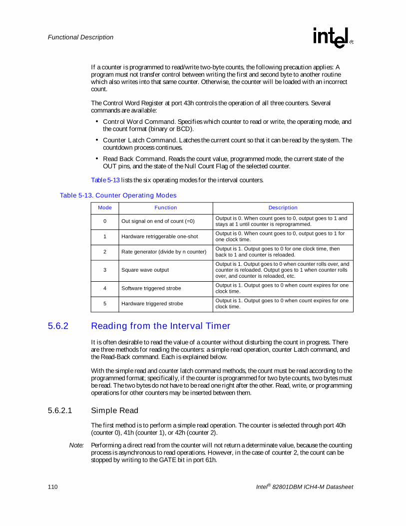
110 Intel® 82801DBM ICH4-M Datasheet
Functional Description
If a counter is programmed to read/write two-byte counts, the following precaution applies: A program must not transfer control between writing the first and second byte to another routine which also writes into that same counter. Otherwise, the counter will be loaded with an incorrect count.
The Control Word Register at port 43h controls the operation of all three counters. Several commands are available:
� Control Word Command. Specifies which counter to read or write, the operating mode, and the count format (binary or BCD).
� Counter Latch Command. Latches the current count so that it can be read by the system. The countdown process continues.
� Read Back Command. Reads the count value, programmed mode, the current state of the OUT pins, and the state of the Null Count Flag of the selected counter.
Table 5-13 lists the six operating modes for the interval counters.
5.6.2 Reading from the Interval TimerIt is often desirable to read the value of a counter without disturbing the count in progress. There are three methods for reading the counters: a simple read operation, counter Latch command, and the Read-Back command. Each is explained below.
With the simple read and counter latch command methods, the count must be read according to the programmed format; specifically, if the counter is programmed for two byte counts, two bytes must be read. The two bytes do not have to be read one right after the other. Read, write, or programming operations for other counters may be inserted between them.
5.6.2.1 Simple Read
The first method is to perform a simple read operation. The counter is selected through port 40h (counter 0), 41h (counter 1), or 42h (counter 2).
Note: Performing a direct read from the counter will not return a determinate value, because the counting process is asynchronous to read operations. However, in the case of counter 2, the count can be stopped by writing to the GATE bit in port 61h.
Table 5-13. Counter Operating Modes
Mode Function Description
0 Out signal on end of count (=0) Output is 0. When count goes to 0, output goes to 1 and stays at 1 until counter is reprogrammed.
1 Hardware retriggerable one-shot Output is 0. When count goes to 0, output goes to 1 for one clock time.
2 Rate generator (divide by n counter) Output is 1. Output goes to 0 for one clock time, then back to 1 and counter is reloaded.
3 Square wave outputOutput is 1. Output goes to 0 when counter rolls over, and counter is reloaded. Output goes to 1 when counter rolls over, and counter is reloaded, etc.
4 Software triggered strobe Output is 1. Output goes to 0 when count expires for one clock time.
5 Hardware triggered strobe Output is 1. Output goes to 0 when count expires for one clock time.

Intel® 82801DBM ICH4-M Datasheet 111
Functional Description
5.6.2.2 Counter Latch Command
The Counter Latch Command, written to port 43h, latches the count of a specific counter at the time the command is received. This command is used to ensure that the count read from the counter is accurate, particularly when reading a two-byte count. The count value is then read from each counter's Count Register as was programmed by the Control Register.
The count is held in the latch until it is read or the counter is reprogrammed. The count is then unlatched. This allows reading the contents of the counters on the fly without affecting counting in progress. Multiple Counter Latch Commands may be used to latch more than one counter. Counter Latch commands do not affect the programmed mode of the counter in any way.
If a Counter is latched and then, some time later, latched again before the count is read, the second Counter Latch command is ignored. The count read will be the count at the time the first Counter Latch command was issued.
5.6.2.3 Read Back Command
The Read Back command, written to port 43h, latches the count value, programmed mode, and current states of the OUT pin and Null Count flag of the selected counter or counters. The value of the counter and its status may then be read by I/O access to the counter address.
The Read Back command may be used to latch multiple counter outputs at one time. This single command is functionally equivalent to several counter latch commands, one for each counter latched. Each counter's latched count is held until it is read or reprogrammed. Once read, a counter is unlatched. The other counters remain latched until they are read. If multiple count Read Back commands are issued to the same counter without reading the count, all but the first are ignored.
The Read Back command may additionally be used to latch status information of selected counters. The status of a counter is accessed by a read from that counter's I/O port address. If multiple counter status latch operations are performed without reading the status, all but the first are ignored.
Both count and status of the selected counters may be latched simultaneously. This is functionally the same as issuing two consecutive, separate Read Back commands. If multiple count and/or status Read Back commands are issued to the same counters without any intervening reads, all but the first are ignored.
If both count and status of a counter are latched, the first read operation from that counter will return the latched status, regardless of which was latched first. The next one or two reads, depending on whether the counter is programmed for one or two type counts, return the latched count. Subsequent reads return unlatched count.

112 Intel® 82801DBM ICH4-M Datasheet
Functional Description
5.7 8259 Interrupt Controllers (PIC) (D31:F0)The ICH4 incorporates the functionality of two 8259 interrupt controllers that provide system interrupts for the ISA compatible interrupts. These interrupts are: system timer, keyboard controller, serial ports, parallel ports, floppy disk, IDE, mouse, and DMA channels. In addition, this interrupt controller can support the PCI based interrupts, by mapping the PCI interrupt onto the compatible ISA interrupt line. Each 8259 core supports eight interrupts, numbered 0�7. Table 5-14 shows how the cores are connected.
.
The ICH4 cascades the slave controller onto the master controller through master controller interrupt input 2. This means there are only 15 possible interrupts for the ICH4 PIC.
Interrupts can individually be programmed to be edge or level, except for IRQ0, IRQ2, IRQ8#, and IRQ13.
Note that previous PIIXn devices internally latched IRQ12 and IRQ1 and required a port 60h read to clear the latch. The ICH4 can be programmed to latch IRQ12 or IRQ1 (see bit 11 and bit 12 in General Control Register, D31:F0, offset D0h).
Table 5-14. Interrupt Controller Core Connections
8259 8259 Input
Typical Interrupt Source Connected Pin / Function
Master
0 Internal Internal Timer / Counter 0 output
1 Keyboard IRQ1 via SERIRQ
2 Internal Slave Controller INTR output
3 Serial Port A IRQ3 via SERIRQ
4 Serial Port B IRQ4 via SERIRQ
5 Parallel Port / Generic IRQ5 via SERIRQ
6 Floppy Disk IRQ6 via SERIRQ
7 Parallel Port / Generic IRQ7 via SERIRQ
Slave
0 Internal Real Time Clock Internal RTC
1 Generic IRQ9 via SERIRQ
2 Generic IRQ10 via SERIRQ
3 Generic IRQ11 via SERIRQ
4 PS/2 Mouse IRQ12 via SERIRQ
5 Internal State Machine output based on processor FERR# assertion.
6 Primary IDE cable IRQ14 from input signal (primary IDE in legacy mode only) or via SERIRQ
7 Secondary IDE Cable IRQ15 from input signal (secondary IDE in legacy mode only) or via SERIRQ
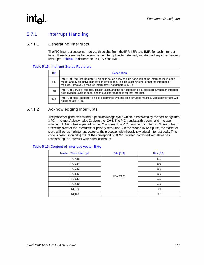
Intel® 82801DBM ICH4-M Datasheet 113
Functional Description
5.7.1 Interrupt Handling
5.7.1.1 Generating Interrupts
The PIC interrupt sequence involves three bits, from the IRR, ISR, and IMR, for each interrupt level. These bits are used to determine the interrupt vector returned, and status of any other pending interrupts. Table 5-15 defines the IRR, ISR and IMR.
5.7.1.2 Acknowledging Interrupts
The processor generates an interrupt acknowledge cycle which is translated by the host bridge into a PCI Interrupt Acknowledge Cycle to the ICH4. The PIC translates this command into two internal INTA# pulses expected by the 8259 cores. The PIC uses the first internal INTA# pulse to freeze the state of the interrupts for priority resolution. On the second INTA# pulse, the master or slave will sends the interrupt vector to the processor with the acknowledged interrupt code. This code is based upon bits [7:3] of the corresponding ICW2 register, combined with three bits representing the interrupt within that controller.
Table 5-15. Interrupt Status Registers
Bit Description
IRRInterrupt Request Register. This bit is set on a low-to-high transition of the interrupt line in edge mode, and by an active high level in level mode. This bit is set whether or not the interrupt is masked. However, a masked interrupt will not generate INTR.
ISR Interrupt Service Register. This bit is set, and the corresponding IRR bit cleared, when an interrupt acknowledge cycle is seen, and the vector returned is for that interrupt.
IMR Interrupt Mask Register. This bit determines whether an interrupt is masked. Masked interrupts will not generate INTR.
Table 5-16. Content of Interrupt Vector Byte
Master, Slave Interrupt Bits [7:3] Bits [2:0]
IRQ7,15
ICW2[7:3]
111
IRQ6,14 110
IRQ5,13 101
IRQ4,12 100
IRQ3,11 011
IRQ2,10 010
IRQ1,9 001
IRQ0,8 000
114 Intel® 82801DBM ICH4-M Datasheet
Functional Description
5.7.1.3 Hardware/Software Interrupt Sequence
1. One or more of the Interrupt Request lines (IRQ) are raised high in edge mode, or seen high in level mode, setting the corresponding IRR bit.
2. The PIC sends INTR active to the processor if an asserted interrupt is not masked.
3. The processor acknowledges the INTR and responds with an interrupt acknowledge cycle. The cycle is translated into a PCI interrupt acknowledge cycle by the host bridge. This command is broadcast over PCI by the ICH4.
4. Upon observing its own interrupt acknowledge cycle on PCI, the ICH4 converts it into the two cycles that the internal 8259 pair can respond to. Each cycle appears as an interrupt acknowledge pulse on the internal INTA# pin of the cascaded interrupt controllers.
5. Upon receiving the first internally generated INTA# pulse, the highest priority ISR bit is set and the corresponding IRR bit is reset. On the trailing edge of the first pulse, a slave identification code is broadcast by the master to the slave on a private, internal three bit wide bus. The slave controller uses these bits to determine if it must respond with an interrupt vector during the second INTA# pulse.
6. Upon receiving the second internally generated INTA# pulse, the PIC returns the interrupt vector. If no interrupt request is present because the request was too short in duration, the PIC will return vector 7 from the master controller.
7. This completes the interrupt cycle. In AEOI mode the ISR bit is reset at the end of the second INTA# pulse. Otherwise, the ISR bit remains set until an appropriate EOI command is issued at the end of the interrupt subroutine.
5.7.2 Initialization Command Words (ICWx)Before operation can begin, each 8259 must be initialized. In the ICH4, this is a four byte sequence. The four initialization command words are referred to by their acronyms: ICW1, ICW2, ICW3, and ICW4.
The base address for each 8259 initialization command word is a fixed location in the I/O memory space: 20h for the master controller, and A0h for the slave controller.
5.7.2.1 ICW1
An I/O write to the master or slave controller base address with data bit 4 equal to 1 is interpreted as a write to ICW1. Upon sensing this write, the ICH4 PIC expects three more byte writes to 21h for the master controller, or A1h for the slave controller, to complete the ICW sequence.
A write to ICW1 starts the initialization sequence during which the following automatically occur:
1. Following initialization, an interrupt request (IRQ) input must make a low-to-high transition to generate an interrupt.
2. The Interrupt Mask Register is cleared.
3. IRQ7 input is assigned priority 7.
4. The slave mode address is set to 7.
5. Special mask mode is cleared and Status Read is set to IRR.

Intel® 82801DBM ICH4-M Datasheet 115
Functional Description
5.7.2.2 ICW2
The second write in the sequence (ICW2) is programmed to provide bits [7:3] of the interrupt vector that will be released during an interrupt acknowledge. A different base is selected for each interrupt controller.
5.7.2.3 ICW3
The third write in the sequence (ICW3) has a different meaning for each controller.
� For the master controller, ICW3 is used to indicate which IRQ input line is used to cascade the slave controller. Within the ICH4, IRQ2 is used. Therefore, bit 2 of ICW3 on the master controller is set to a 1, and the other bits are set to 0s.
� For the slave controller, ICW3 is the slave identification code used during an interrupt acknowledge cycle. On interrupt acknowledge cycles, the master controller broadcasts a code to the slave controller if the cascaded interrupt won arbitration on the master controller. The slave controller compares this identification code to the value stored in its ICW3, and if it matches, the slave controller assumes responsibility for broadcasting the interrupt vector.
5.7.2.4 ICW4
The final write in the sequence, ICW4, must be programmed both controllers. At the very least, bit 0 must be set to a 1 to indicate that the controllers are operating in an Intel Architecture-based system.
5.7.3 Operation Command Words (OCW)These command words reprogram the Interrupt Controller to operate in various interrupt modes.
� OCW1 masks and unmasks interrupt lines.
� OCW2 controls the rotation of interrupt priorities when in rotating priority mode and controls the EOI function.
� OCW3 is sets up ISR/IRR reads, enables/disables the special mask mode (SMM) and enables/disables polled interrupt mode.
5.7.4 Modes of Operation
5.7.4.1 Fully Nested Mode
In this mode, interrupt requests are ordered in priority from 0 through 7, with 0 being the highest. When an interrupt is acknowledged, the highest priority request is determined and its vector placed on the bus. Additionally, the ISR for the interrupt is set. This ISR bit remains set until: the processor issues an EOI command immediately before returning from the service routine; or if in AEOI mode, on the trailing edge of the second INTA#. While the ISR bit is set, all further interrupts of the same or lower priority are inhibited, while higher levels will generate another interrupt. Interrupt priorities can be changed in the rotating priority mode.

116 Intel® 82801DBM ICH4-M Datasheet
Functional Description
5.7.4.2 Special Fully-Nested Mode
This mode will be used in the case of a system where cascading is used, and the priority has to be conserved within each slave. In this case, the special fully-nested mode will be programmed to the master controller. This mode is similar to the fully-nested mode with the following exceptions:
� When an interrupt request from a certain slave is in service, this slave is not locked out from the master's priority logic and further interrupt requests from higher priority interrupts within the slave will be recognized by the master and will initiate interrupts to the processor. In the normal-nested mode, a slave is masked out when its request is in service.
� When exiting the Interrupt Service routine, software has to check whether the interrupt serviced was the only one from that slave. This is done by sending a Non-Specific EOI command to the slave and then reading its ISR. If it is 0, a non-specific EOI can also be sent to the master.
5.7.4.3 Automatic Rotation Mode (Equal Priority Devices)
In some applications, there are a number of interrupting devices of equal priority. Automatic rotation mode provides for a sequential 8-way rotation. In this mode, a device receives the lowest priority after being serviced. In the worst case, a device requesting an interrupt will have to wait until each of seven other devices are serviced at most once.
There are two ways to accomplish automatic rotation using OCW2; the Rotation on Non-Specific EOI Command (R=1, SL=0, EOI=1) and the rotate in automatic EOI mode, which is set by (R=1, SL=0, EOI=0).
5.7.4.4 Specific Rotation Mode (Specific Priority)
Software can change interrupt priorities by programming the bottom priority. For example, if IRQ5 is programmed as the bottom priority device, then IRQ6 will be the highest priority device. The Set Priority Command is issued in OCW2 to accomplish this, where: R=1, SL=1, and LO-L2 is the binary priority level code of the bottom priority device.
In this mode, internal status is updated by software control during OCW2. However, it is independent of the EOI command. Priority changes can be executed during an EOI command by using the Rotate on Specific EOI Command in OCW2 (R=1, SL=1, EOI=1 and LO-L2=IRQ level to receive bottom priority.
5.7.4.5 Poll Mode
Poll mode can be used to conserve space in the interrupt vector table. Multiple interrupts that can be serviced by one interrupt service routine do not need separate vectors if the service routine uses the poll command. Poll mode can also be used to expand the number of interrupts. The polling interrupt service routine can call the appropriate service routine, instead of providing the interrupt vectors in the vector table. In this mode the INTR output is not used and the microprocessor internal Interrupt Enable flip-flop is reset, disabling its interrupt input. Service to devices is achieved by software using a Poll command.
The Poll command is issued by setting P=1 in OCW3. The PIC treats its next I/O read as an interrupt acknowledge, sets the appropriate ISR bit if there is a request, and reads the priority level. Interrupts are frozen from the OCW3 write to the I/O read. The byte returned during the I/O read will contain a 1 in bit 7 if there is an interrupt, and the binary code of the highest priority level in bits 2:0.

Intel® 82801DBM ICH4-M Datasheet 117
Functional Description
5.7.4.6 Cascade Mode
The PIC in the ICH4 has one master 8259 and one slave 8259 cascaded onto the master through IRQ2. This configuration can handle up to 15 separate priority levels. The master controls the slaves through a three bit internal bus. In the ICH4, when the master drives 010b on this bus, the slave controller takes responsibility for returning the interrupt vector. An EOI command must be issued twice: once for the master and once for the slave.
5.7.4.7 Edge and Level Triggered Mode
In ISA systems this mode is programmed using bit 3 in ICW1, which sets level or edge for the entire controller. In the ICH4, this bit is disabled and a new register for edge and level triggered mode selection, per interrupt input, is included. This is the Edge/Level control Registers ELCR1 and ELCR2.
If an ELCR bit is 0, an interrupt request will be recognized by a low-to-high transition on the corresponding IRQ input. The IRQ input can remain high without generating another interrupt. If an ELCR bit is 1, an interrupt request will be recognized by a high level on the corresponding IRQ input and there is no need for an edge detection. The interrupt request must be removed before the EOI command is issued to prevent a second interrupt from occurring.
In both the edge and level triggered modes, the IRQ inputs must remain active until after the falling edge of the first internal INTA#. If the IRQ input goes inactive before this time, a default IRQ7 vector will be returned.
5.7.4.8 End of Interrupt Operations
An EOI can occur in one of two fashions: by a command word write issued to the PIC before returning from a service routine, the EOI command; or automatically when AEOI bit in ICW4 is set to 1.
5.7.4.9 Normal End of Interrupt
In Normal EOI, software writes an EOI command before leaving the interrupt service routine to mark the interrupt as completed. There are two forms of EOI commands: Specific and Non-Specific. When a Non-Specific EOI command is issued, the PIC will clear the highest ISR bit of those that are set to 1. Non-Specific EOI is the normal mode of operation of the PIC within the ICH4, as the interrupt being serviced currently is the interrupt entered with the interrupt acknowledge. When the PIC is operated in modes which preserve the fully nested structure, software can determine which ISR bit to clear by issuing a Specific EOI. An ISR bit that is masked will not be cleared by a Non-Specific EOI if the PIC is in the special mask mode. An EOI command must be issued for both the master and slave controller.
5.7.4.10 Automatic End of Interrupt Mode
In this mode, the PIC will automatically perform a Non-Specific EOI operation at the trailing edge of the last interrupt acknowledge pulse. From a system standpoint, this mode should be used only when a nested multi-level interrupt structure is not required within a single PIC. The AEOI mode can only be used in the master controller and not the slave controller.

118 Intel® 82801DBM ICH4-M Datasheet
Functional Description
5.7.5 Masking Interrupts
5.7.5.1 Masking on an Individual Interrupt Request
Each interrupt request can be masked individually by the Interrupt Mask Register (IMR). This register is programmed through OCW1. Each bit in the IMR masks one interrupt channel. Masking IRQ2 on the master controller will mask all requests for service from the slave controller.
5.7.5.2 Special Mask Mode
Some applications may require an interrupt service routine to dynamically alter the system priority structure during its execution under software control. For example, the routine may wish to inhibit lower priority requests for a portion of its execution but enable some of them for another portion.
The special mask mode enables all interrupts not masked by a bit set in the Mask Register. Normally, when an interrupt service routine acknowledges an interrupt without issuing an EOI to clear the ISR bit, the interrupt controller inhibits all lower priority requests. In the special mask mode, any interrupts may be selectively enabled by loading the Mask Register with the appropriate pattern. The special mask mode is set by OCW3 where: SSMM=1, SMM=1, and cleared where SSMM=1, SMM=0.
5.7.6 Steering PCI InterruptsThe ICH4 can be programmed to allow PIRQA#-PIRQH# to be internally routed to interrupts 3-7, 9-12, 14 or 15. The assignment is programmable through the PIRQx Route Control registers, located at 60-63h and 68-6Bh in function 0. One or more PIRQx# lines can be routed to the same IRQx input. If interrupt steering is not required, the Route Registers can be programmed to disable steering.
The PIRQx# lines are defined as active low, level sensitive to allow multiple interrupts on a PCI Board to share a single line across the connector. When a PIRQx# is routed to specified IRQ line, software must change the IRQ's corresponding ELCR bit to level sensitive mode. The ICH4 will internally invert the PIRQx# line to send an active high level to the PIC. When a PCI interrupt is routed onto the PIC, the selected IRQ can no longer be used by an ISA device (through SERIRQ). However, active low non-ISA interrupts can share their interrupt with PCI interrupts.
Internal sources of the PIRQs, including SCI and TCO interrupts, cause the external PIRQ to be asserted. The ICH4 receives the PIRQ input, like all of the other external sources, and routes it accordingly.

Intel® 82801DBM ICH4-M Datasheet 119
Functional Description
5.8 Advanced Interrupt Controller (APIC) (D31:F0)In addition to the standard ISA-compatible interrupt controller (PIC) described in Section 5.7, the ICH4 incorporates the Advanced Programmable Interrupt Controller (APIC). While the standard interrupt controller is intended for use in a uni-processor system, APIC can be used in either a uni-processor or multi-processor system.
5.8.1 Interrupt HandlingThe I/O APIC handles interrupts very differently than the 8259. Briefly, these differences are:
� Method of Interrupt Transmission. The I/O APIC transmits interrupts through a three wire bus, and interrupts are handled without the need for the processor to run an interrupt acknowledge cycle.
� Interrupt Priority. The priority of interrupts in the I/O APIC is independent of the interrupt number. For example, interrupt 10 can be given a higher priority than interrupt 3.
� More Interrupts. The I/O APIC in the ICH4 supports a total of 24 interrupts.
� Multiple Interrupt Controllers. The I/O APIC interrupt transmission protocol has an arbitration phase, which allows for multiple I/O APICs in the system with their own interrupt vectors. The ICH4 I/O APIC must arbitrate for the APIC bus before transmitting its interrupt message.
5.8.2 Interrupt MappingThe I/O APIC within the ICH4 supports 24 APIC interrupts. Each interrupt has its own unique vector assigned by software. The interrupt vectors are mapped as follows, and match �Config 6� of the Multi-Processor Specification.
Table 5-17. APIC Interrupt Mapping (Sheet 1 of 2)
IRQ # Via SERIRQ
Direct from pin
Via PCI message Internal Modules
0 No No No Cascade from 8259 #1
1 Yes No Yes
2 No No No 8254 Counter 0
3 Yes No Yes
4 Yes No Yes
5 Yes No Yes
6 Yes No Yes
7 Yes No Yes
8 No No No RTC
9 Yes No Yes Option for SCI, TCO
10 Yes No Yes Option for SCI, TCO
11 Yes No Yes Option for SCI, TCO
12 Yes No Yes

120 Intel® 82801DBM ICH4-M Datasheet
Functional Description
NOTES:1. IRQ 14 and 15 can only be driven directly from the pins when in legacy IDE mode.2. When programming the polarity of internal interrupt sources on the APIC, interrupts 0 through 15 receive
active-high internal interrupt sources, while interrupts 16 through 23 receive active-low internal interrupt sources.
5.8.3 APIC Bus Functional Description
5.8.3.1 Physical Characteristics of APIC
The APIC bus is a 3-wire synchronous bus connecting all I/O and local APICs. Two of these wires are used for data transmission, and one wire is a clock. For bus arbitration, the APIC uses only one of the data wires. The bus is logically a wire-OR and electrically an open-drain connection providing for both bus use arbitration and arbitration for lowest priority. The APIC bus speed can run from 16.67 MHz to 33 MHz.
5.8.3.2 APIC Bus Arbitration
The I/O APIC uses one wire arbitration to win bus ownership. A rotating priority scheme is used for APIC bus arbitration. The winner of the arbitration becomes the lowest priority agent and assumes an arbitration ID of 0. All other agents, except the agent whose arbitration ID is 15, increment their Arbitration IDs by one. The agent whose ID was 15 will take the winner's arbitration ID and will increment it by one. Arbitration IDs are changed only for messages that are transmitted successfully (except for the Low Priority messages). A message is transmitted successfully if no CS error or acceptance error was reported for that message.
An APIC agent can use two different priority schemes: Normal or EOI. EOI has the highest priority. EOI priority is used to send EOI messages for level interrupts from a local APIC to an I/O APIC. When an agent requests the bus with EOI priority, all other agents requesting the bus with normal priorities will back off.
13 No No No FERR# logic
14 Yes Yes1 Yes
15 Yes Yes1 Yes
16 PIRQ[A]# PIRQ[A]# No USB UHCI Controller #1
17 PIRQ[B]# PIRQ[B]# No AC �97 Audio, Modem, option for SMbus
18 PIRQ[C]# PIRQ[C]# No USB UHCI Controller #3, Native IDE
19 PIRQ[D]# PIRQ[D]# No USB UHCI Controller #2
20 N/A PIRQ[E]# Yes LAN, option for SCI, TCO
21 N/A PIRQ[F]# Yes Option for SCI, TCO
22 N/A PIRQ[G]# Yes Option for SCI, TCO
23 N/A PIRQ[H]# Yes USB EHCI Controller, option for SCI, TCO
Table 5-17. APIC Interrupt Mapping (Sheet 2 of 2)
IRQ # Via SERIRQ
Direct from pin
Via PCI message Internal Modules

Intel® 82801DBM ICH4-M Datasheet 121
Functional Description
When ICH4 detects a bus idle condition on the APIC Bus, and it has an interrupt to send over the APIC bus, it drives a start cycle to begin arbitration by driving bit 0 to a 0 on an APICCLK rising edge. It then samples bit 1. If Bit 1 was a 0, then a local APIC started arbitration for an EOI message on the same clock edge that the ICH4 started arbitration. The ICH4 has, thus, lost arbitration and will stop driving the APIC bus.
If the ICH4 did not see an EOI message start, it will start transferring its arbitration ID, located in bits [27:24] of its Arbitration ID register (ARBID). Starting in Cycle 2, through Cycle 5, it will tri-state bit 0, and drive bit 1 to a 0 if ARBID[27] is a 1. If ARBID[27] is a 0, it will also tri-state bit 1. At the end of each cycle, the ICH4 will sample the state of Bit 1 on the APIC bus. If the ICH4 did not drive Bit 1 (ARBID[27] = 0), and it samples a 0, then another APIC agent started arbitration for the APIC bus at the same time as the ICH4, and it has higher priority. The ICH4 will stop driving the APIC bus. Table 5-18 describes the arbitration cycles.
5.8.3.3 Bus Message Formats
After bus arbitration, the winner is granted exclusive use of the bus and will drive its message. APIC messages come in four formats, determined by the Delivery Mode bits. These four messages are of different length, and are known by all APICs on the bus through the transmission of the Delivery Mode bits.
Table 5-18. Arbitration Cycles
Cycle Bit 1 Bit 0 Comment
1 EOI 0 Bit 1 = 1: Normal, Bit 1 = 0: EOI
2 NOT (ARBID[27]) 1
Arbitration ID. If ICH4 samples a different value than it sent, it lost arbitration.
3 NOT (ARBID[26]) 1
4 NOT (ARBID[25]) 1
5 NOT (ARBID[24]) 1
Table 5-19. APIC Message Formats
Message # of Cycles
Delivery Mode Bits Comments
EOI 14 xxxEnd of Interrupt transmission from Local APIC to I/O APIC on Level interrupts. EOI is known by the EOI bit at the start of arbitration.
Short 21 001, 010, 100, 101, 111
I/O APIC delivery on Fixed, NMI, SMI, Reset, ExtINT, and Lowest Priority with focus processor messages.
Lowest Priority 33 001 Transmission of Lowest Priority interrupts when the status field indicates that the processor does not have focus.
Remote Read 39 011 Message from one Local APIC to another to read registers.

122 Intel® 82801DBM ICH4-M Datasheet
Functional Description
EOI Message for Level Triggered Interrupts
EOI messages are used by local APICs to send an EOI cycle occurring for a level-triggered interrupt to an I/O APIC. This message is needed so that the I/O APIC can differentiate between a new interrupt on the interrupt line versus the same interrupt on the interrupt line. The target of the EOI is given by the local APIC through the transmission of the priority vector (V7 through V0) of the interrupt. Upon receiving this message, the I/O APIC resets the Remote IRR bit for that interrupt. If the interrupt signal is still active after the IRR bit is reset, the I/O APIC will treat it as a new interrupt.
Table 5-20. EOI Message
Cycle Bit 1 Bit 0 Comments
1 0 0 EOI message
2�5 ARBID 1 Arbitration ID
6 NOT(V7) NOT(V6) Interrupt vector bits V7 - V0 from redirection table register
7 NOT(V5) NOT(V4)
8 NOT(V3) NOT(V2)
9 NOT(V1) NOT(V0)
10 NOT(C1) NOT(C0) Check Sum from Cycles 6�9
11 1 1 Postamble
12 NOT(A) NOT(A) Status Cycle 0
13 NOT(A1) NOT(A1) Status Cycle 1
14 1 1 Idle

Intel® 82801DBM ICH4-M Datasheet 123
Functional Description
Short Message
Short messages are used for the delivery of Fixed, NMI, SMI, Reset, ExtINT, and Lowest Priority with Focus processor interrupts. The Delivery Mode bits (M2�M0) specify the message. All short messages take 21 cycles including the idle cycle.
NOTES:1. If DM is 0 (physical mode), cycles 15 and 16 are the APIC ID and cycles 13 and 14 are sent as 1. If DM is 1
(logical mode), cycles 13 through 16 are the 8-bit Destination field. The interpretation of the logical mode 8-bit Destination field is performed by the local units using the Destination Format Register. Shorthands of �all-incl-self� and �all-excl-self� both use physical destination mode and a destination field containing APIC ID value of all ones. The sending APIC knows whether it should (incl) or should not (excl) respond to its own message.
2. The checksum field is the cumulative add (mod 4) of all data bits (DM, M0�3, L, TM, V0�7, D0�7). The APIC driving the message provides this checksum. This, in essence, is the lower two bits of an adder at the end of the message.
3. This cycle allows all APICs to perform various internal computations based on the information contained in the received message. One of the computations takes the checksum of the data received in cycles 6 through 16 and compares it with the value in cycle 18. If any APIC computes a different checksum than the one passed in cycle 17, then that APIC will signal an error on the APIC bus (�00�) in cycle 19. If this happens, all APICs will assume the message was never sent and the sender must try sending the message again, which includes re-arbitrating for the APIC bus. In lowest priority delivery when the interrupt has a focus processor, the focus processor will signal this by driving a 01 during cycle 19. This tells all the other APICs that the interrupt has been accepted, the arbitration is preempted, and short message format is used. Cycle 19 and 20 indicates the status of the message (i.e., accepted, check sum error, retry, or error). Table 5-22 shows the status signal combinations and their meanings for all delivery modes.
Table 5-21. Short Message
Cycle Bit 1 Bit 0 Comments
1 1 0 Normal Arbitration
2�5 ARBID 1 Arbitration ID
6 NOT(DM) NOT(M2) DM1 = Destination Mode from bit 11 of the redirection table register
7 NOT(M1) NOT(M0) M2-M0 = Delivery Mode from bits 10:8 of the redirection table register
8 NOT(L) NOT(TM) L = Level, TM = Trigger Mode
9 NOT(V7) NOT(V6)
Interrupt vector bits V7 - V0 from redirection table register10 NOT(V5) NOT(V4)
11 NOT(V3) NOT(V2)
12 NOT(V1) NOT(V0)
13 NOT(D7) NOT(D6)
Destination field from bits 63:56 of redirection table register114 NOT(D5) NOT(D4)
15 NOT(D3) NOT(D2)
16 NOT(D1) NOT(D0)
17 NOT(C1) NOT(C0) Checksum for Cycles 6�162
18 1 1 Postamble3
19 NOT(A) NOT(A) Status Cycle 0. See Table 5-22.
20 NOT(A1) NOT(A1) Status Cycle 1. See Table 5-22.
21 1 1 Idle

124 Intel® 82801DBM ICH4-M Datasheet
Functional Description
Table 5-22. APIC Bus Status Cycle Definition
Delivery Mode A Comments A1 Comments
Fixed, EOI
11 Checksum OK 1x Error
01 Accepted
00 Retry
10 Error xx
01 Error xx
00 Checksum Error xx
NMI, SMM, Reset, ExtINT
11 Checksum OK 1x Error
01 Accepted
00 Error
10 Error xx
01 Error xx
00 Checksum Error xx
Lowest Priority
11 Checksum OK: No Focus Processor 1x Error
01 End and Retry
00 Go for Low Priority Arbitration
10 Error xx
01 Checksum OK: Focus Processor xx
00 Checksum Error xx
Remote Read
11 Checksum OK xx
10 Error xx
01 Error xx
00 Checksum Error xx

Intel® 82801DBM ICH4-M Datasheet 125
Functional Description
Lowest Priority without Focus Processor (FP) Message
This message format is used to deliver an interrupt in the lowest priority mode in which it does not have a Focus Process. Cycles 1 through 21 for this message is same as for the short message discussed above. Status cycle 19 identifies if there is a Focus processor (10) and a status value of 11 in cycle 20 indicates the need for lowest priority arbitration.
NOTES:1. Cycle 21 through 28 are used to arbitrate for the lowest priority processor. The processor that takes part in
the arbitration drives the processor priority on the bus. Only the local APICs that have "free interrupt slots" will participate in the lowest priority arbitration.
2. Cycles 29 through 32 are used to break a tie in case two more processors have lowest priority. The bus arbitration IDs are used to break the tie.
Table 5-23. Lowest Priority Message (Without Focus Processor)
Cycle Bit 1 Bit 0 Comments
1 1 0 Normal Arbitration2�5 ARBID 1 Arbitration ID
6 NOT(DM) NOT(M2) DM = Destination Mode from bit 11 of the redirection table register
7 NOT(M1) NOT(M0) M2-M0 = Delivery Mode from bits 10:8 of the redirection table register
8 NOT(L) NOT(TM) L = Level, TM = Trigger Mode9 NOT(V7) NOT(V6)
Interrupt vector bits V7�V0 from redirection table register10 NOT(V5) NOT(V4)11 NOT(V3) NOT(V2)
12 NOT(V1) NOT(V0)13 NOT(D7) NOT(D6)
Destination field from bits 63:56 of redirection table register14 NOT(D5) NOT(D4)15 NOT(D3) NOT(D2)
16 NOT(D1) NOT(D0)17 NOT(C1) NOT(C0) Checksum for Cycles 6�1618 1 1 Postamble19 NOT(A) NOT(A) Status Cycle 0.
20 NOT(A1) NOT(A1) Status Cycle 1.21 P7 1
Inverted Processor Priority P7�P0
22 P6 123 P5 1
24 P4 125 P3 126 P2 127 P1 1
28 P0 129 ArbID3 130 ArbID2 131 ArbID1 1
32 ArbID0 133 S S Status34 1 1 Idle

126 Intel® 82801DBM ICH4-M Datasheet
Functional Description
Remote Read Message
Remote read message is used when a local APIC wishes to read the register in another local APIC. The I/O APIC in the ICH4 neither generates or responds to this cycle. The message format is same as short message for the first 21 cycles.
NOTE: Cycle 21 through 36 contain the remote register data. The status information in cycle 37 specifies if the data is good or not. Remote read cycle is always successful (although the data may be valid or invalid) in that it is never retried. The reason for this is that Remote Read is a debug feature, and a "hung" remote APIC that is unable to respond should not cause the debugger to hang.
Table 5-24. Remote Read MessageCycle Bit 1 Bit 0 Comments
1 1 0 Normal Arbitration2�5 ARBID 1 Arbitration ID6 NOT(DM) NOT(M2) DM = Destination Mode from bit 11 of the redirection table register
7 NOT(M1) NOT(M0) M2-M0 = Delivery Mode from bits 10:8 of the redirection table register
8 NOT(L) NOT(TM) L = Level, TM = Trigger Mode9 NOT(V7) NOT(V6)
Interrupt vector bits V7�V0 from redirection table register10 NOT(V5) NOT(V4)11 NOT(V3) NOT(V2)12 NOT(V1) NOT(V0)13 NOT(D7) NOT(D6)
Destination field from bits 63:56 of redirection table register14 NOT(D5) NOT(D4)15 NOT(D3) NOT(D2)16 NOT(D1) NOT(D0)17 NOT(C1) NOT(C0) Checksum for Cycles 6�1618 1 1 Postamble19 NOT(A) NOT(A) Status Cycle 0.20 NOT(A1) NOT(A1) Status Cycle 1.21 d31 d30
Remote register data 31-0
22 d29 d2823 d27 d2624 d25 d2425 d23 d2226 d21 d2027 d19 d1828 d17 d1629 d15 d1430 d13 d1231 d11 d1032 d09 d0833 d07 d0634 d05 d0435 d03 d0236 d01 d0037 S S Data Status: 00 = valid, 11 = invalid38 C C Check Sum for data d31-d0039 1 1 Idle

Intel® 82801DBM ICH4-M Datasheet 127
Functional Description
5.8.4 PCI Message-Based Interrupts
5.8.4.1 Theory of Operation
The following scheme is only supported when the internal I/O(x) APIC is used (rather than just the 8259).
The ICH4 supports the new method for PCI devices to deliver interrupts as write cycles, rather than using the traditional PIRQ[A:D] signals. Essentially, the PCI devices are given a write path directly to a register that will cause the desired interrupt. This mode is only supported when the ICH4�s internal I/O APIC is enabled. Upon recognizing the write from the peripheral, the ICH4 sends the interrupt message to the processor using the I/O APIC�s serial bus.
The interrupts associated with the PCI Message-based interrupt method must be set up for edge triggered mode, rather than level triggered, since the peripheral only does the write to indicate the edge.
The following sequence is used:
1. During PCI PnP, the PCI peripheral is first programmed with an address (MESSAGE_ADDRESS) and data value (MESSAGE_DATA) that will be used for the interrupt message delivery. For the ICH4, the MESSAGE_ADDRESS is the IRQ Pin Assertion Register, which is mapped to memory location FEC0_0020h.
2. To cause the interrupt, the PCI peripheral requests the PCI bus and when granted, writes the MESSAGE_DATA value to the location indicated by the MESSAGE_ADDRESS. The MESSAGE_DATA value indicates which interrupt occurred. This MESSAGE_DATA value is a binary encoded. For example, to indicate that interrupt 7 should go active, the peripheral writes a binary value of 0000111. The MESSAGE_DATA is a 32-bit value, although only the lower 5 bits are used.
3. If the PRQ bit in the APIC Version register is set, the ICH4 positively decodes the cycles (as a slave) in medium time.
4. The ICH4 decodes the binary value written to MESSAGE_ADDRESS and sets the appropriate IRR bit in the internal I/O APIC. The corresponding interrupt must be set up for edge-triggered interrupts. The ICH4 supports interrupts 00h through 23h. Binary values outside this range will not cause any action.
5. After sending the interrupt message to the processor, the ICH4 automatically clears the interrupt.
Because they are edge-triggered, the interrupts that are allocated to the PCI bus for this scheme may not be shared with any other interrupt (e.g., the standard PCI PIRQ[A:D], those received via SERIRQ#, or the internal level-triggered interrupts such as SCI or TCO).
The ICH4 ignores interrupt messages sent by PCI masters that attempt to use IRQ0, 2, 8, or 13.
128 Intel® 82801DBM ICH4-M Datasheet
Functional Description
5.8.4.2 Registers and Bits Associated with PCI Interrupt Delivery
Capabilities Indication
The capability to support PCI interrupt delivery is indicated via ACPI configuration techniques. This involves the BIOS creating a data structure that gets reported to the ACPI configuration software. The OS reads the PRQ bit in the APIC Version Register to see if the ICH4 is capable of support PCI-based interrupt messages. As a precaution, the PRQ bit is not set if the XAPIC_EN bit is not set.
Interrupt Message Register
The PCI devices all write their message into the IRQ Pin Assertion Register, which is a memory-Mapped register located at the APIC base memory location + 20h.
5.8.5 Processor System Bus Interrupt Delivery
5.8.5.1 Theory of Operation
For processors that support Processor System Bus interrupt delivery, the ICH4 has an option to let the integrated I/O APIC behave as an I/O (x) APIC. In this case, it will deliver interrupt messages to the processor in a parallel manner, rather than using the I/O APIC serial scheme. The ICH4 is intended to be compatible with the I/O (x) APIC specification, Rev 1.1.
This is done by the ICH4 writing (via the Hub Interface) to a memory location that is snooped by the processor(s). The processor(s) snoop the cycle to know which interrupt goes active.
The processor enables the mode by setting the I/O APIC Enable (APIC_EN) bit and by setting the DT bit in the I/O APIC ID register.
The following sequence is used:
1. When the ICH4 detects an interrupt event (active edge for edge-triggered mode or a change for level-triggered mode), it sets or resets the internal IRR bit associated with that interrupt.
2. Internally, the ICH4 requests to use the bus in a way that automatically flushes upstream buffers. This can be internally implemented similar to a DMA device request.
3. The ICH4 then delivers the message by performing a write cycle to the appropriate address with the appropriate data. The address and data formats are described below in Section 5.8.5.5.
Note: PSB Interrupt Delivery compatibility with processor clock control depends on the processor, not the ICH4.
5.8.5.2 Edge-Triggered Operation
In this case, the �Assert Message� is sent when there is an inactive-to-active edge on the interrupt.
5.8.5.3 Level-Triggered Operation
In this case, the �Assert Message� is sent when there is an inactive-to-active edge on the interrupt. If after the EOI the interrupt is still active, then another �Assert Message� is sent to indicate that the interrupt is still active.

Intel® 82801DBM ICH4-M Datasheet 129
Functional Description
5.8.5.4 Registers Associated with Processor System Bus Interrupt Delivery
Capabilities Indication
The capability to support Processor System Bus interrupt delivery is indicated via ACPI configuration techniques. This involves the BIOS creating a data structure that gets reported to the ACPI configuration software.
DT Bit in the Boot Configuration Register
This enables the ICH4 to deliver interrupts as memory writes. This bit is ignored if the APIC mode is not enabled.
5.8.5.5 Interrupt Message Format
The ICH4 writes the message to PCI (and to the Host Controller) as a 32-bit memory write cycle. It uses the formats shown in Table 5-25 and Table 5-26 for the Address and Data.
The local APIC (in the processor) has a delivery mode option to interpret Processor System Bus messages as a SMI in which case the processor treats the incoming interrupt as a SMI instead of as an interrupt. This does not mean that the ICH4 has any way to have a SMI source from ICH4 power management logic cause the I/OAPIC to send an SMI message (there is no way to do this). The ICH4�s I/OAPIC can only send interrupts due to interrupts which do not include SMI, NMI or INIT. This means that in IA32/IA64 based platforms, Processor System Bus interrupt message format delivery modes 010 (SMI/PMI), 100 (NMI), and 101 (INIT) as indicated in this section, must not be used and is not supported. Only the hardware pin connection is supported by ICH4.
:
Table 5-25. Interrupt Message Address Format
Bit Description
31:20 Will always be FEEh
19:12 Destination ID: This will be the same as bits 63:56 of the I/O Redirection Table entry for the interrupt associated with this message.
11:4 Extended Destination ID: This will be the same as bits 55:48 of the I/O Redirection Table entry for the interrupt associated with this message.
3
Redirection Hint: This bit is used by the processor host bridge to allow the interrupt message to be redirected.0 = The message will be delivered to the agent (processor) listed in bits 19:12.1 = The message will be delivered to an agent with a lower interrupt priority This can be derived
from bits 10:8 in the Data Field (see below).The Redirection Hint bit will be a 1 if bits 10:8 in the delivery mode field associated with corresponding interrupt are encoded as 001 (Lowest Priority). Otherwise, the Redirection Hint bit will be 0.
2
Destination Mode: This bit is used only when the Redirection Hint bit is set to 1. If the Redirection Hint bit and the Destination Mode bit are both set to 1, then the logical destination mode is used, and the redirection is limited only to those processors that are part of the logical group as based on the logical ID.
1:0 Will always be 00.

130 Intel® 82801DBM ICH4-M Datasheet
Functional Description
5.9 Serial Interrupt (D31:F0)The ICH4 supports a serial IRQ scheme. This allows a single signal to be used to report interrupt requests. The signal used to transmit this information is shared between the host, the ICH4, and all peripherals that support serial interrupts. The signal line, SERIRQ, is synchronous to PCI clock, and follows the sustained tri-state protocol that is used by all PCI signals. This means that if a device has driven SERIRQ low, it will first drive it high synchronous to PCI clock and release it the following PCI clock. The serial IRQ protocol defines this sustained tri-state signaling in the following fashion:
� S - Sample Phase. Signal driven low� R - Recovery Phase. Signal driven high� T - Turn-around Phase. Signal released
The ICH4 supports a message for 21 serial interrupts. These represent the 15 ISA interrupts (IRQ[0:1, 2:15]), the four PCI interrupts, and the control signals SMI# and IOCHK#. The serial IRQ protocol does not support the additional APIC interrupts (20�23).
Note: When the IDE primary and secondary controllers are configured for native IDE mode, the only way to use the internal IRQ14 and IRQ15 connections to the Interrupt Controllers is through the Serial Interrupt pin.
Table 5-26. Interrupt Message Data Format
Bit Description
31:16 Will always be 0000h.
15 Trigger Mode: 1 = Level, 0 = Edge. Same as the corresponding bit in the I/O Redirection Table for that interrupt.
14Delivery Status: 1 = Assert, 0 = Deassert.If using edge-triggered interrupts, then bit will always be 1, since only the assertion is sent.If using level-triggered interrupts, then this bit indicates the state of the interrupt input.
13:12 Will always be 00.
11 Destination Mode: 1 = Logical. 0 = Physical. Same as the corresponding bit in the I/O Redirection Table for that interrupt.
10:8
Delivery Mode: This is the same as the corresponding bits in the I/O Redirection Table for that interrupt.000 = Fixed 100 = NMI001 = Lowest Priority 101 = INIT010 = SMI/PMI 110 = Reserved011 = Reserved 111 = ExtINT
7:0 Vector: This is the same as the corresponding bits in the I/O Redirection Table for that interrupt.

Intel® 82801DBM ICH4-M Datasheet 131
Functional Description
5.9.1 Start FrameThe serial IRQ protocol has two modes of operation which affect the start frame. These two modes are: Continuous, where the ICH4 is solely responsible for generating the start frame; and Quiet, where a serial IRQ peripheral is responsible for beginning the start frame.
The mode that must first be entered when enabling the serial IRQ protocol is continuous mode. In this mode, the ICH4 asserts the start frame. This start frame is 4, 6, or 8 PCI clocks wide based upon the Serial IRQ Control Register (bits 1:0 at 64h in Device 31:Function 0 configuration space). This is a polling mode.
When the serial IRQ stream enters quiet mode (signaled in the Stop Frame), the SERIRQ line remains inactive and pulled up between the Stop and Start Frame until a peripheral drives the SERIRQ signal low. The ICH4 senses the line low and continues to drive it low for the remainder of the Start Frame. Since the first PCI clock of the start frame was driven by the peripheral in this mode, the ICH4 drives the SERIRQ line low for 1 PCI clock less than in continuous mode. This mode of operation allows for a quiet, and, therefore, lower power operation.
5.9.2 Data FramesOnce the Start frame has been initiated, all of the SERIRQ peripherals must start counting frames based on the rising edge of SERIRQ. Each of the IRQ/DATA frames has exactly 3 phases of 1 clock each:
� Sample Phase. During this phase, the SERIRQ device drives SERIRQ low if the corresponding interrupt signal is low. If the corresponding interrupt is high, then the SERIRQ devices will tri-state the SERIRQ signal. The SERIRQ line will remain high due to pull-up resistors (there is no internal pull-up resistor on this signal, an external pull-up resistor is required). A low level during the IRQ0-1 and IRQ2-15 frames indicates that an active-high ISA interrupt is not being requested, but a low level during the PCI INT[A:D], SMI#, and IOCHK# frame indicates that an active-low interrupt is being requested.
� Recovery Phase. During this phase, the device drives the SERIRQ line high if in the Sample Phase it was driven low. If it was not driven in the sample phase, it will be tri-stated in this phase.
� Turn-around Phase. The device will tri-state the SERIRQ line.
5.9.3 Stop FrameAfter all data frames, a Stop Frame are driven by the ICH4. The SERIRQ signal is driven low by the ICH4 for 2 or 3 PCI clocks. The number of clocks is determined by the SERIRQ configuration register. The number of clocks determines the next mode:
Table 5-27. Stop Frame Explanation
Stop Frame Width Next Mode
2 PCI clocks Quiet Mode. Any SERIRQ device may initiate a Start Frame
3 PCI clocks Continuous Mode. Only the host (ICH4) may initiate a Start Frame

132 Intel® 82801DBM ICH4-M Datasheet
Functional Description
5.9.4 Specific Interrupts Not Supported via SERIRQThere are three interrupts seen through the serial stream which are not supported by the ICH4. These interrupts are generated internally and are not sharable with other devices within the system. These interrupts are:
� IRQ0. Heartbeat interrupt generated off of the internal 8254 counter 0.
� IRQ8#. RTC interrupt can only be generated internally.
� IRQ13. Floating point error interrupt generated off of the processor assertion of FERR#.
The ICH4 ignores the state of these interrupts in the serial stream, and does not adjust their level based on the level seen in the serial stream. In addition, the interrupts IRQ14 and IRQ15 from the serial stream are treated differently than their ISA counterparts. These two frames are not passed to the Bus Master IDE logic. The Bus Master IDE logic expects IDE to be behind the ICH4.
5.9.5 Data Frame FormatTable 5-28 shows the format of the data frames. For the PCI interrupts (A�D), the output from the ICH4 is ANDed with the PCI input signal. This way, the interrupt can be signaled via both the PCI interrupt input signal and via the SERIRQ signal (they are shared).
Table 5-28. Data Frame Format
Data Frame # Interrupt Clocks Past
Start Frame Comment
1 IRQ0 2 Ignored. IRQ0 can only be generated via the internal 8524
2 IRQ1 5
3 SMI# 8 Causes SMI# if low. Will set the SERIRQ_SMI_STS bit.
4 IRQ3 11
5 IRQ4 14
6 IRQ5 17
7 IRQ6 20
8 IRQ7 23
9 IRQ8 26 Ignored. IRQ8# can only be generated internally or on ISA.
10 IRQ9 29
11 IRQ10 32
12 IRQ11 35
13 IRQ12 38
14 IRQ13 41 Ignored. IRQ13 can only be generated from FERR#
15 IRQ14 44 Do not include in BM IDE interrupt logic
16 IRQ15 47 Do not include in BM IDE interrupt logic
17 IOCHCK# 50 Same as ISA IOCHCK# going active.
18 PCI INTA# 53 Drive PIRQA#
19 PCI INTB# 56 Drive PIRQB#
20 PCI INTC# 59 Drive PIRQC#
21 PCI INTD# 62 Drive PIRQD#

Intel® 82801DBM ICH4-M Datasheet 133
Functional Description
5.10 Real Time Clock (D31:F0)The Real Time Clock (RTC) module provides a battery backed-up date and time keeping device with two banks of static RAM with 128 bytes each, although the first bank has 114 bytes for general purpose usage. Three interrupt features are available: time of day alarm with once a second to once a month range, periodic rates of 122 µs to 500 ms, and end of update cycle notification. Seconds, minutes, hours, days, day of week, month, and year are counted. Daylight savings compensation is optional. The hour is represented in twelve or twenty-four hour format, and data can be represented in BCD or binary format. The design is meant to be functionally compatible with the Motorola* MS146818B. The time keeping comes from a 32.768 kHz oscillating source, which is divided to achieve an update every second. The lower 14 bytes on the lower RAM block has very specific functions. The first ten are for time and date information. The next four (0Ah to 0Dh) are registers, which configure and report RTC functions.
The time and calendar data should match the data mode (BCD or binary) and hour mode (12 or 24 hour) as selected in register B. It is up to the programmer to make sure that data stored in these locations is within the reasonable values ranges and represents a possible date and time. The exception to these ranges is to store a value of C0�FF in the Alarm bytes to indicate a don�t care situation. All Alarm conditions must match to trigger an Alarm Flag, which could trigger an Alarm Interrupt if enabled. The SET bit must be one while programming these locations to avoid clashes with an update cycle. Access to time and date information is done through the RAM locations. If a RAM read from the ten time and date bytes is attempted during an update cycle, the value read will not necessarily represent the true contents of those locations. Any RAM writes under the same conditions will be ignored.
Note: The ICH4 supports the ability to generate an SMI# based on Year 2000 rollover. See Section 5.10.4 for more information on the century rollover.
The ICH4 does not implement month/year alarms.
5.10.1 Update CyclesAn update cycle occurs once a second, if the SET bit of register B is not asserted and the divide chain is properly configured. During this procedure, the stored time and date will be incremented, overflow will be checked, a matching alarm condition will be checked, and the time and date will be rewritten to the RAM locations. The update cycle will start at least 488 µs after the UIP bit of register A is asserted, and the entire cycle will not take more than 1984 µs to complete. The time and date RAM locations (0�9) will be disconnected from the external bus during this time.
To avoid update and data corruption conditions, external RAM access to these locations can safely occur at two times. When a updated-ended interrupt is detected, almost 999 ms is available to read and write the valid time and date data. If the UIP bit of Register A is detected to be low, there is at least 488 µs before the update cycle begins.
Warning: The overflow conditions for leap years and daylight savings adjustments are based on more than one date or time item. To ensure proper operation when adjusting the time, the new time and data values should be set at least two seconds before one of these conditions (leap year, daylight savings time adjustments) occurs.

134 Intel® 82801DBM ICH4-M Datasheet
Functional Description
5.10.2 InterruptsThe real-time clock interrupt is internally routed within the ICH4 both to the I/O APIC and the 8259. It is mapped to interrupt vector 8. This interrupt does not leave the ICH4, nor is it shared with any other interrupt. IRQ8# from the SERIRQ stream is ignored.
5.10.3 Lockable RAM RangesThe RTC�s battery-backed RAM supports two 8-byte ranges that can be locked via the configuration space. If the locking bits are set, the corresponding range in the RAM will not be readable or writable. A write cycle to those locations will have no effect. A read cycle to those locations will not return the location�s actual value (may be all 0s or all 1s).
Once a range is locked, the range can be unlocked only by a hard reset, which will invoke the BIOS and allow it to relock the RAM range.
5.10.4 Century RolloverThe ICH4 detects a rollover when the Year byte (RTC I/O space, index offset 09h) transitions form 99 to 00. Upon detecting the rollover, the ICH4 will set the NEWCENTURY_STS bit (TCOBASE + 04h, bit 7). If the system is in an S0 state, this will cause an SMI#. The SMI# handler can update registers in the RTC RAM that are associated with century value. If the system is in a sleep state (S1-M�S5) when the century rollover occurs, the ICH4 will also set the NEWCENTURY_STS bit, but no SMI# is generated. When the system resumes from the sleep state, BIOS should check the NEWCENTURY_STS bit and update the century value in the RTC RAM.
5.10.5 Clearing Battery-Backed RTC RAMClearing CMOS RAM in an ICH4-based platform can be done by using a jumper on RTCRST# or GPI, or using SAFEMODE strap. Implementations should not attempt to clear CMOS by using a jumper to pull VccRTC low.
Using RTCRST# to clear CMOS
A jumper on RTCRST# can be used to clear CMOS values, as well as reset to default, the state of those configuration bits that reside in the RTC power well. When the RTCRST# is strapped to ground, the RTC_PWR_STS bit (D31:F0:A4h bit 2) is set and those configuration bits in the RTC power well will be set to their default state. BIOS can monitor the state of this bit and manually clear the RTC CMOS array once the system is booted. The normal position would cause RTCRST# to be pulled up through a weak pull-up resistor. Table 5-29 shows which bits are set to their default state when RTCRST# is asserted.
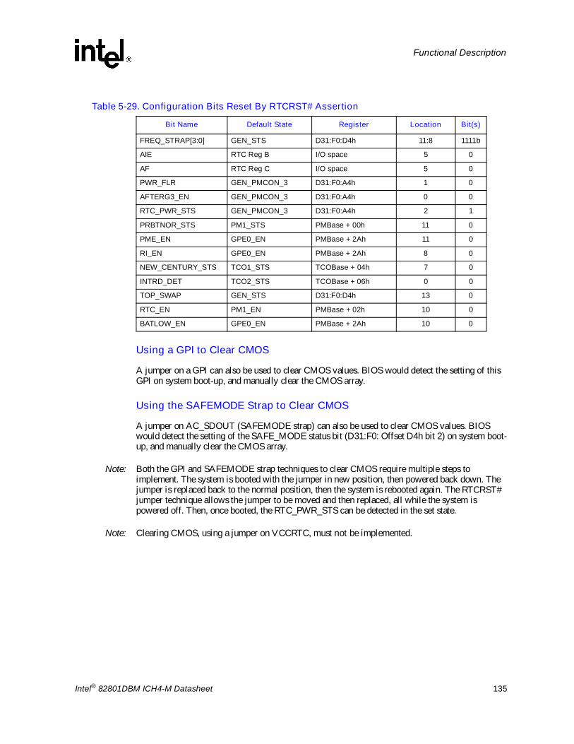
Intel® 82801DBM ICH4-M Datasheet 135
Functional Description
Using a GPI to Clear CMOS
A jumper on a GPI can also be used to clear CMOS values. BIOS would detect the setting of this GPI on system boot-up, and manually clear the CMOS array.
Using the SAFEMODE Strap to Clear CMOS
A jumper on AC_SDOUT (SAFEMODE strap) can also be used to clear CMOS values. BIOS would detect the setting of the SAFE_MODE status bit (D31:F0: Offset D4h bit 2) on system boot-up, and manually clear the CMOS array.
Note: Both the GPI and SAFEMODE strap techniques to clear CMOS require multiple steps to implement. The system is booted with the jumper in new position, then powered back down. The jumper is replaced back to the normal position, then the system is rebooted again. The RTCRST# jumper technique allows the jumper to be moved and then replaced, all while the system is powered off. Then, once booted, the RTC_PWR_STS can be detected in the set state.
Note: Clearing CMOS, using a jumper on VCCRTC, must not be implemented.
Table 5-29. Configuration Bits Reset By RTCRST# Assertion
Bit Name Default State Register Location Bit(s)
FREQ_STRAP[3:0] GEN_STS D31:F0:D4h 11:8 1111b
AIE RTC Reg B I/O space 5 0
AF RTC Reg C I/O space 5 0
PWR_FLR GEN_PMCON_3 D31:F0:A4h 1 0
AFTERG3_EN GEN_PMCON_3 D31:F0:A4h 0 0
RTC_PWR_STS GEN_PMCON_3 D31:F0:A4h 2 1
PRBTNOR_STS PM1_STS PMBase + 00h 11 0
PME_EN GPE0_EN PMBase + 2Ah 11 0
RI_EN GPE0_EN PMBase + 2Ah 8 0
NEW_CENTURY_STS TCO1_STS TCOBase + 04h 7 0
INTRD_DET TCO2_STS TCOBase + 06h 0 0
TOP_SWAP GEN_STS D31:F0:D4h 13 0
RTC_EN PM1_EN PMBase + 02h 10 0
BATLOW_EN GPE0_EN PMBase + 2Ah 10 0

136 Intel® 82801DBM ICH4-M Datasheet
Functional Description
5.11 Processor Interface (D31:F0)The ICH4 interfaces to the processor with a variety of signals
� Standard Outputs to processor: A20M#, SMI#, NMI, INIT#, INTR, STPCLK#, IGNNE#, CPUSLP#
� Standard Input from processor: FERR#
� Intel SpeedStep technology Output to processor: CPUPWRGOOD
Most ICH4 outputs to the processor use standard buffers. The ICH4 has a separate VCC signal which is pulled up at the system level to the processor voltage, and thus determines VOH for the outputs to the processor. Note that this is different than previous generations of chips, that have used open-drain outputs. This new method saves up to 12 external pull-up resistors.
The ICH4 also handles the speed setting for the processor by holding specific signals at certain states just prior to CPURST going inactive. This avoids the glue often required with other chipsets.
The ICH4 does not support the processor�s FRC mode.
5.11.1 Processor Interface SignalsThis section describes each of the signals that interface between the ICH4 and the processor(s). Note that the behavior of some signals may vary during processor reset, as the signals are used for frequency strapping.
5.11.1.1 A20M#
The A20M# signal will be active (low) when both of the following conditions are true:
� The ALT_A20_GATE bit (Bit 1 of PORT92 register) is a 0
� The A20GATE input signal is a 0
The A20GATE input signal is expected to be generated by the external microcontroller (KBC).
5.11.1.2 INIT#
The INIT# signal will be active (driven low) based on any one of several events described in Table 5-30. When any of these events occur, INIT# will be driven low for 16 PCI clocks, then driven high.
Note: The 16-clock counter for INIT# assertion will halt while STPCLK# is active. Therefore, if INIT# is supposed to go active while STPCLK# is asserted, it will actually go active after STPCLK# goes inactive.

Intel® 82801DBM ICH4-M Datasheet 137
Functional Description
5.11.1.3 FERR#/IGNNE# (Coprocessor Error)
The ICH4 supports the coprocessor error function with the FERR#/IGNNE# pins. The function is enabled via the COPROC_ERR_EN bit (Device 31:Function 0, Offset D0, bit 13). FERR# is tied directly to the Coprocessor Error signal of the processor. If FERR# is driven active by the processor, IRQ13 goes active (internally). When it detects a write to the COPROC_ERR register, the ICH4 negates the internal IRQ13 and drives IGNNE# active. IGNNE# remains active until FERR# is driven inactive. IGNNE# is never driven active unless FERR# is active.
If COPROC_ERR_EN is not set, then the assertion of FERR# will have not generate an internal IRQ13, nor will the write to F0h generate IGNNE#.
Table 5-30. INIT# Going Active
Cause of INIT# Going Active Comment
Shutdown special cycle from processor.
PORT92 write, where INIT_NOW (bit 0) transitions from a 0 to a 1.
PORTCF9 write, where SYS_RST (bit 1) was a 0 and RST_CPU (bit 2) transitions from 0 to 1.
RCIN# input signal goes low. RCIN# is expected to be driven by the external microcontroller (KBC).
0 to 1 transition on RCIN# must occur before the ICH4 will arm INIT# to be generated again.NOTE: RCIN# signal is expected to be high during
S1-M and low during S3, S4, and S5 states. Transition on the RCIN# signal in those states (or the transition to those states) may not necessarily cause the INIT# signal to be generated to the processor.
CPU BISTTo enter BIST, the software sets CPU_BIST_EN bit and then does a full processor reset using the CF9 register.
Figure 5-12. Coprocessor Error Timing Diagram
FERR#
Internal IRQ13
I/O Write to F0h
IGNNE#

138 Intel® 82801DBM ICH4-M Datasheet
Functional Description
5.11.1.4 NMI
Non-Maskable Interrupts (NMIs) can be generated by several sources, as described in Table 5-31.
5.11.1.5 STPCLK# and CPUSLP# Signals
The ICH4 power management logic controls these active-low signals. Refer to Section 5.12 for more information on the functionality of these signals.
5.11.1.6 CPUPWRGOOD Signal
This signal is connected to the processor�s PWRGOOD input. To allow for Intel SpeedStep technology support, this signal is kept high during an Intel SpeedStep technology state transition to prevent loss of processor context. This is an open-drain output signal (external pull-up resistor required) that represents a logical AND of the ICH4�s PWROK and VGATE / VRMPWRGD signals.
5.11.1.7 DPSLP#
This active-low signal controls the internal gating of the processor�s core clock. This signal behaves identically to the STP_CPU# signal to effectively stop the processor�s clock (internally) in the states in which STP_CPU# can be used to stop the processor�s clock externally.
Table 5-31. NMI Sources
Cause of NMI Comment
SERR# goes active (either internally, externally via SERR# signal, or via message from the MCH)
Can instead be routed to generate an SCI, through the NMI2SCI_EN bit (Device 31:Function 0, offset 4E, bit 11).
IOCHK# goes active via SERIRQ# stream(ISA system Error)
Can instead be routed to generate an SCI, through the NMI2SCI_EN bit (Device 31:Function 0, offset 4E, bit 11).

Intel® 82801DBM ICH4-M Datasheet 139
Functional Description
5.11.2 Speed Strapping for ProcessorThe ICH4 directly sets the speed straps for the processor, saving the external logic that has been needed with prior PCIsets. Refer to processor specification for speed strapping definition.
The ICH4 performs the following to set the speed straps for the processor:
1. While PCIRST# is active, the ICH4 drives A20M#, IGNNE#, NMI, and INTR high.
2. As soon as PWROK goes active, the ICH4 reads the FREQ_STRAP field contents.
3. The next step depends on the power state being exited as described in Table 5-32.
NOTE: The FREQ_STRAP register is in the RTC well. The value in the register can be forced to 1111h via a pinstrap (AC_SDOUT signal), or the ICH4 can automatically force the speed strapping to 1111h if the processor fails to boot.
Table 5-32. Frequency Strap Behavior Based on Exit State
State Exiting ICH4
S1-M There is no processor reset, so no frequency strap logic is used.
S3, S4, S5, or G3
Based on PWROK going active, the ICH4 will deassert PCIRST#, and based on the value of the FREQ_STRAP field (D31:F0,Offset D5h (BACK_CNTL)), the ICH4 will drive the intended core frequency values on A20M#, IGNNE#, NMI, and INTR.
Table 5-33. Frequency Strap Bit Mapping
FREQ_STRAP Bits [3:0] Sets High/Low Level for the Corresponding Signal
3 NMI
2 INTR
1 IGNNE#
0 A20M#
Figure 5-13. Signal Strapping
Processor
ICH4
A20M#, IGNNE#,INTR, NMI
Host Controller
4x 2 to 1Mux
FrequencyStrap Register
PCIRST#
PWROK
INIT#
CPURST#

140 Intel® 82801DBM ICH4-M Datasheet
Functional Description
5.12 Power Management (D31:F0)The power management features include:
� ACPI Power and Thermal Management Support� ACPI 24-Bit Timer� Software initiated throttling of processor performance for Thermal and Power Reduction� Hardware Override to throttle processor performance if system too hot� SCI and SMI# Generation
� PCI PME# Signal for Wake Up from Low-Power states� System Clock Control
� ACPI C2 state: Quickstart state (using STPCLK# signal) halts processor�s instruction stream
� ACPI C3 State: Ability to halt processor clock (but not hub interface or memory clock)
� ACPI C4 State: Ability to lower processor voltage.
� CLKRUN# Protocol for PCI Clock Starting/Stopping� System Sleeping State Control
� ACPI S1-M state: Powered On Suspend (POS)
� Ability to lower processor voltage during S1 - Mobile to reduce leakage (Deeper Sleep)� ACPI S3 state: Suspend to RAM (STR)� ACPI S4 state: Suspend-to-Disk (STD)� ACPI G2/S5 state: Soft Off (SOFF)� Power Failure Detection and Recovery
� Streamlined Legacy Power Management Support for APM-Based Systems
� Intel SpeedStep technology transition logic

Intel® 82801DBM ICH4-M Datasheet 141
Functional Description
5.12.1 Intel® ICH4 and System Power States Table 5-34 shows the power states defined for ICH4-based platforms. The state names generally match the corresponding ACPI states.
Table 5-34. General Power States for Systems Using Intel® ICH4
State/Substates Legacy Name / Description
G0/S0/C0
Full On: Processor operating. Individual devices may be shut down to save power. The different processor operating levels are defined by Cx states, as shown in Table 5-35. Within the C0 state, the ICH4 can throttle the STPCLK# signal to reduce power consumption. The throttling can be initiated by software or by the THRM# input signal.
G0/S0/C1 Auto-Halt: Processor has executed a AutoHalt instruction and is not executing code. The processor snoops the bus and maintains cache coherency.
G0/S0/C2Quickstart: The STPCLK# signal goes active to the processor. The processor performs a Stop-Grant cycle, halts its instruction stream, and remains in that state until the STPCLK# signal goes inactive. In the Quickstart state, the processor snoops the bus and maintains cache coherency.
G0/S0/C3
Stop-Clock: The STPCLK# signal goes active to the processor. The processor performs a Stop-Grant cycle, halts its instruction stream. ICH4 then asserts STP_CPU#, which forces the clock generator to stop the processor clock. This is also used for Intel SpeedStep technology support. Accesses to memory (by AGP, PCI, or internal units) is not permitted while in a C3 state. It is assumed that the ARB_DIS bit is set prior to entering C3 state.
G0/S0/C4Stop-Clock with lower Processor voltage. This closely resembles the G0/S0/C3 state. However, after the ICH4 has asserted STP_CPU#, it then lowers the voltage to the processor. This reduces the leakage on the processor. Prior to exiting the C4 state, the ICH4 increases the voltage to the processor.
G1/S1-M
Powered-On-Suspend (POS): In this state, all clocks (except the 32.768 kHz clock) are stopped. The system context is maintained in system DRAM. Power is maintained to PCI, the processor, memory controller, memory, and all other critical subsystems. Note that this state does not preclude power being removed from non-essential devices (e.g., disk drives).During this state, the processor can be selected for either Deep Sleep or Deeper Sleep.In Deeper Sleep, the processor voltage is reduced in this state to reduce the leakage power.
G1/S3 Suspend-To-RAM (STR): The system context is maintained in system DRAM, but power is shut off to non-critical circuits. Memory is retained, and refreshes continue. All clocks stop except RTC clock.
G1/S4 Suspend-To-Disk (STD): The context of the system is maintained on the disk. All power is then shut off to the system except for the logic required to resume.
G2/S5 Soft Off (SOFF): System context is not maintained. All power is shut off except for the logic required to restart. A full boot is required when waking.
G3
Mechanical OFF (MOFF): System context not maintained. All power is shut off except for the RTC. No �Wake� events are possible, because the system does not have any power. This state occurs if the user removes the batteries, turns off a mechanical switch, or if the system power supply is at a level that is insufficient to power the �waking� logic. When system power returns, transition will depends on the state just prior to the entry to G3 and the AFTERG3 bit in the GEN_PMCON3 register (D31:F0, offset A4). Refer to Table 5-42 for more details.
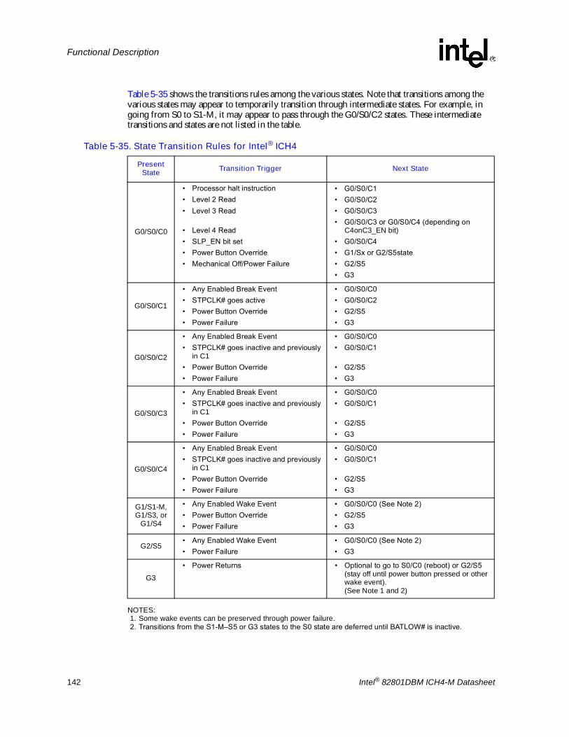
142 Intel® 82801DBM ICH4-M Datasheet
Functional Description
Table 5-35 shows the transitions rules among the various states. Note that transitions among the various states may appear to temporarily transition through intermediate states. For example, in going from S0 to S1-M, it may appear to pass through the G0/S0/C2 states. These intermediate transitions and states are not listed in the table.
NOTES:1. Some wake events can be preserved through power failure.2. Transitions from the S1-M�S5 or G3 states to the S0 state are deferred until BATLOW# is inactive.
Table 5-35. State Transition Rules for Intel® ICH4
Present State Transition Trigger Next State
G0/S0/C0
� Processor halt instruction� Level 2 Read� Level 3 Read
� Level 4 Read� SLP_EN bit set� Power Button Override� Mechanical Off/Power Failure
� G0/S0/C1� G0/S0/C2� G0/S0/C3� G0/S0/C3 or G0/S0/C4 (depending on
C4onC3_EN bit)� G0/S0/C4� G1/Sx or G2/S5state� G2/S5� G3
G0/S0/C1
� Any Enabled Break Event� STPCLK# goes active� Power Button Override� Power Failure
� G0/S0/C0� G0/S0/C2� G2/S5� G3
G0/S0/C2
� Any Enabled Break Event� STPCLK# goes inactive and previously
in C1� Power Button Override� Power Failure
� G0/S0/C0� G0/S0/C1
� G2/S5� G3
G0/S0/C3
� Any Enabled Break Event� STPCLK# goes inactive and previously
in C1� Power Button Override� Power Failure
� G0/S0/C0� G0/S0/C1
� G2/S5� G3
G0/S0/C4
� Any Enabled Break Event� STPCLK# goes inactive and previously
in C1� Power Button Override� Power Failure
� G0/S0/C0� G0/S0/C1
� G2/S5� G3
G1/S1-M,G1/S3, or
G1/S4
� Any Enabled Wake Event� Power Button Override� Power Failure
� G0/S0/C0 (See Note 2)� G2/S5� G3
G2/S5� Any Enabled Wake Event� Power Failure
� G0/S0/C0 (See Note 2)� G3
G3� Power Returns � Optional to go to S0/C0 (reboot) or G2/S5
(stay off until power button pressed or other wake event). (See Note 1 and 2)

Intel® 82801DBM ICH4-M Datasheet 143
Functional Description
5.12.2 System Power PlanesThe system has several independent power planes, as described in Table 5-36. Note that when a particular power plane is shut off, it should go to a 0-V level.
s
5.12.3 Intel® ICH4 Power PlanesThe ICH4 power planes are defined in Section 4.1. Although there are not specific power planes within the ICH4, there are many interface signals that go to devices that may be powered down. These include:
� IDE: ICH4 can tri-state or drive low all IDE output signals and shut off input buffers.
� USB: ICH4 can tri-state USB output signals and shut off input buffers if USB wakeup is not desired
� AC �97: ICH4 can drive low the outputs and shut off inputs
5.12.4 SMI#/SCI GenerationUpon any SMI# event taking place, ICH4 asserts SMI# to the processor which causes it to enter SMM space. SMI# remains active until the EOS bit is set. When the EOS bit is set, SMI# goes inactive for a minimum of 4 PCICLK. If another SMI event occurs, SMI# is driven active again.
The SCI is a level-mode interrupt that is typically handled by an ACPI-aware operating system. In non-APIC systems (which is the default), the SCI IRQ is routed to one of the 8259 interrupts (IRQ 9, 10, or 11). The 8259 interrupt controller must be programmed to level mode for that interrupt.
In systems using the APIC, the SCI can be routed to interrupts 9, 10, 11, 20, 21, 22, or 23. The interrupt polarity changes depending on whether it is on an interrupt shareable with a PIRQ or not; (see Section 9.1.11 ACPI Control Register for details.) The interrupt will remain asserted until all SCI sources are removed.
Table 5-36. System Power Plane
Plane Controlled By Description
Processor SLP_S3# signal
SLP_S1# puts the clock generator into a low-power state, but does not cut the power to the processor. The SLP_S3# signal can be used to cut the processor�s power completely. The new Deeper Sleep support allows lowering the processor�s voltage during the C4 or S1-M states.
MAIN SLP_S3# signal
When SLP_S3# goes active, power can be shut off to any circuit not required to wake the system from the S3 state. Since the S3 state requires that the memory context be preserved, power must be retained to the main memory.The processor, devices on the PCI bus, LPC interface downstream hub interface and AGP will typically be shut off when the Main power plane is shut, although there may be small subsections powered.
MEMORY SLP_S4# signal
When the SLP_S4# goes active, power can be shut off to any circuit not required to wake the system from the S4. Since the memory context does not need to be preserved in the S4 state, the power to the memory can also be shut down.
DEVICE[n] GPIOIndividual subsystems may have their own power plane. For example, GPIO signals may be used to control the power to disk drives, audio amplifiers, or the display screen.

144 Intel® 82801DBM ICH4-M Datasheet
Functional Description
Table 5-37 shows which events can cause an SMI# and SCI. Note that some events can be programmed to cause either an SMI# or SCI. The usage of the event for SCI (instead of SMI#) is typically associated with an ACPI-based system. Each SMI# or SCI source has a corresponding enable and status bit.
Table 5-37. Causes of SMI# and SCI (Sheet 1 of 2)
Cause SCI SMI Additional Enables Where Reported
PME# Yes Yes PME_EN=1 PME_STS
PME_B0 (internal EHCI controller) Yes Yes PME_B0_EN=1 PME_B0_STS
Power Button Press Yes Yes PWRBTN_EN=1 PWRBTN_STS
RTC Alarm Yes Yes RTC_EN=1 RTC_STS
Ring Indicate Yes Yes RI_EN=1 RI_STS
AC �97 wakes Yes Yes AC �97_EN=1 AC �97_STS
USB UHCI #1 wakes Yes Yes USB1_EN=1 USB1_STS
USB UHCI #2 wakes Yes Yes USB2_EN=1 USB2_STS
USB UHCI #3 wakes Yes Yes USB3_EN=1 USB3_STS
THRM# pin active Yes Yes THRM_EN=1 THRM_STS
ACPI Timer overflow (2.34 sec.) Yes Yes TMROF_EN=1 TMROF_STS
Any GPI Yes YesGPI[x]_Route=10 (SCI)GPI[x]_Route=01 (SMI)
GPE0[x]_EN=1
GPI[x]_STSGPE0_STS
TCO SCI Logic Yes No TCOSCI_EN=1 TCOSCI_STS
TCO SCI message from MCH Yes No none MCHSCI_STS
TCO SMI Logic No Yes TCO_EN=1 TCO_STS
TCO SMI -Year 2000 Rollover No Yes none NEWCENTURY_STS
TCO SMI -TCO TIMEROUT No Yes none TIMEOUT
TCO SMI - OS writes to TCO_DAT_IN register No Yes none OS_TCO_SMI
TCO SMI -Message from MCH No Yes none MCHSMI_STS
TCO SMI - NMI occurred (and NMIs mapped to SMI) No Yes NMI2SMI_EN=1 NMI2SMI_STS
TCO SMI -INTRUDER# signal goes active No Yes INTRD_SEL=10 INTRD_DET
TCO SMI - Change of the BIOSWP bit from 0 to 1 No Yes BLD=1 BIOSWR_STS
TCO SMI -Write attempted to BIOS No Yes BIOSWP=1 BIOSWR_STS
BIOS_RLS written to Yes No GBL_EN=1 GBL_STS
GBL_RLS written to No Yes BIOS_EN=1 BIOS_STS
Write to B2h register No Yes none APM_STS
Periodic timer expires No Yes PERIODIC_EN=1 PERIODIC_STS
64 ms timer expires No Yes SWSMI_TMR_EN=1 SWSMI_TMR_STS
Enhanced USB Legacy Support Event No Yes LEGACY_USB2_EN = 1 LEGACY_USB2_STS
Enhanced USB Intel Specific Event No Yes INTEL_USB2_EN = 1 INTEL_USB2_STS
Classic USB Legacy logic No Yes LEGACY_USB_EN=1 LEGACY_USB_STS
Serial IRQ SMI reported No Yes none SERIRQ_SMI_STS

Intel® 82801DBM ICH4-M Datasheet 145
Functional Description
NOTES:1. SCI_EN must be 1 to enable SCI. SCI_EN must be 0 to enable SMI.2. SCI can be routed to cause interrupt 9:11 or 20:23 (20:23 only available in APIC mode).3. GBL_SMI_EN must be 1 to enable SMI.4. EOS must be written to 1 to re-enable SMI for the next one.
5.12.5 Dynamic Processor Clock ControlThe ICH4 has extensive control for dynamically starting and stopping system clocks. The clock control is used for transitions among the various S0/Cx states, and processor throttling. Each dynamic clock control method is described in this section. The various Sleep states may also perform types of non-dynamic clock control.
The ICH4 supports the ACPI C0, C1, C3, and C4 states.
The Dynamic processor clock control is handled using the following signals:
� STPCLK#: Used to halt processor instruction stream.
� C3_STAT#: Used to signal an AGP device that the system is about to enter, or has just exited a C3 state.
� STP_CPU#: Used to stop processor�s clock
� CPUSLP#: Must be asserted prior to STP_CPU# (in stop grant mode)
� DPSLP#: Used to force Deeper Sleep for processor.
� DPRSLPVR: Used to lower voltage of VRM during C4 state and optional for S1-M.
The C1 state is entered based on the processor performing an auto halt instruction. The C2 state is entered based on the processor reading the Level 2 register in the ICH4.
The C3 state is entered based on the processor reading the Level 3 register in the ICH4. Note that an Intel SpeedStep technology transition may appear to temporarily pass through a C3 state, however it is a separate transition and documented separately in Section 5.12.9
The C4 state is entered based on the processor reading the Level 4 register in the ICH4, or by reading the Level 3 register when the C4onC3_EN bit is set.
Device monitors match address in its range No Yes DEV[n]_TRAP_EN=1 DEVMON_STS,
DEV[n]_TRAP_STS
SMBus Host Controller No Yes SMB_SMI_ENHost Controller Enabled SMBus host status reg.
SMBus Slave SMI message No Yes none SMBUS_SMI_STS
SMBus SMBALERT# signal active No Yes none SMBUS_SMI_STS
SMBus Host Notify message received No Yes HOST_NOTIFY_INTREN SMBUS_SMI_STS
HOST_NOTIFY_STS
BATLOW# assertion Yes Yes BATLOW_EN=1. BATLOW_STS
Access microcontroller 62h/66h No Yes MCSMI_EN MCSMI_STS
SLP_EN bit written to 1 No Yes SMI_ON_SLP_EN=1 SMI_ON_SLP_EN_STS
Table 5-37. Causes of SMI# and SCI (Sheet 2 of 2)
Cause SCI SMI Additional Enables Where Reported

146 Intel® 82801DBM ICH4-M Datasheet
Functional Description
A C1, C2, C3, or C4 state ends due to a Break event. Based on the break event, the ICH4 returns the system to C0 state. Table 5-38 lists the possible break events from C2, C3, or C4. The break events from C1 are indicated in the processor�s datasheet.
The ICH4 supports the Pending Break Event (PBE) indication from the processor using the FERR# signal. The following rules apply:
1. When STPCLK# is detected active by the processor, the FERR# signal from the processor will be redefined to indicate whether an interrupt is pending. The signal is active low (i.e., FERR# will be low to indicate a pending interrupt).
2. When the ICH4 asserts STPCLK#, it will latch the current state of the FERR# signal and continue to present this state to the FERR# state machine (independent of what the FERR# pin does after the latching).
3. When the ICH4 detects the Stop-Grant cycle, it will start looking at the FERR# signal as a break event indication. If FERR# is sampled low, a break event is indicated. This will force a transition to the C0 state.
4. When the processor detects the deassertion of STPCLK#, the processor will start driving the FERR# signal with the natural value (i.e., the value it would do if the pin was not muxed). The time from STPCLK# inactive to the FERR# signal transition back to the native function must be less than 120 ns.
5. The ICH4 waits at least 180 ns after deasserting STPCLK# and then starts using the FERR# signal for an indication of a floating point error. The maximum time that the ICH4 may wait is bounded such that it must have a chance to look at the FERR# signal before reasserting STPCLK#. Based on current implementation, that maximum time would be 240 ns (8 PCI clocks).
The break event associated with this new mechanism does not need to set any particular status bit, since the pending interrupt will be serviced by the processor after returning to the C0 state.
Table 5-38. Break Events
Event Breaks from Comment
Any unmasked interrupt goes active C2, C3, C4IRQ[0:15] when using the 8259s, IRQ[0:23] for I/O APIC. Since SCI is an interrupt, any SCI will also be a break event.
Any internal event that will cause an NMI or SMI# C2, C3, C4 Many possible sources
Any internal event that will cause INIT# to go active C2, C3, C4 Could be indicated by the keyboard controller
via the RCIN input signal.
Any bus master request (internal, external or DMA) goes active and BM_RLD=1
C3, C4 Need to wake up processor so it can do snoops.
Processor Pending Break Event Indication C2, C3, C4
Only available if FERR# enabled for break event indication (See GEN_CNTL.FERR# Mux-En bit in Section 9.1.22).
Intel® 82801DBM ICH4-M Datasheet 147
Functional Description
5.12.5.1 Throttling Using STPCLK#
Throttling is used to lower power consumption or reduce heat. The ICH4 asserts STPCLK# to throttle the processor clock and the processor appears to temporarily enter a C2 state. After a programmable time, the ICH4 deasserts STPCLK# and the processor appears to return to the C0 state. This allows the processor to operate at reduced average power, with a corresponding decrease in performance. Two methods are included to start throttling:
1. Software enables a timer with a programmable duty cycle. The duty cycle is set by the THTL_DTY field and the throttling is enabled using the THTL_EN field. This is known as Manual Throttling. The period is fixed to be in the non-audible range, due to the nature of switching power supplies.
2. A Thermal Override condition (THRM# signal active for >2 seconds) occurs that unconditionally forces throttling, independent of the THTL_EN bit. The throttling due to Thermal Override has a separate duty cycle (THRM_DTY) which may vary by field and system. The Thermal Override condition will end when THRM# goes inactive.
Throttling due to the THRM# signal has higher priority than the software-initiated throttling. Throttling does not occur when the system is in a C2, C3, or C4, even if Thermal override occurs.
5.12.5.2 Transition Rules among S0/Cx and Throttling States
The following priority rules and assumptions apply among the various S0/Cx and throttling states:
� Entry to any S0/Cx state is mutually exclusive with entry to any S1-M�S5 state. This is because the processor can only perform one register access at a time and Sleep states have higher priority than thermal throttling.
� When the SLP_EN bit is set (system going to a sleep state (S1-M�S5), the THTL_EN bit can be internally treated as being disabled (no throttling while going to sleep state). Note that thermal throttling (based on THRM# signal) cannot be disabled in an S0 state. However, once the SLP_EN bit is set, the thermal throttling is shut off (since STPCLK# will be active in S1-M�S5 states).
� If the THTL_EN bit is set, and a Level 2, Level 3, or Level 4 read then occurs, the system should immediately go and stay in aC2, C3, or C4 state until a break event occurs. A Level 2, Level 3 or Level 4 read has higher priority than the software initiated throttling or thermal throttling.
� If Thermal Override is causing throttling, and a Level 2, Level 3, or Level 4 read then occurs, the system will stay in a C2, C3, or C4 state until a break event occurs. A Level 2, Level 3 or Level 4 read has higher priority than the Thermal Override.
� After an exit from a C2, C3, or C4 state (due to a Break event), and if the THTL_EN bit is still set, or if a Thermal Override is still occurring, the system will continue to throttle STPCLK#. Depending on the time of break event, the first transition on STPCLK# active can be delayed by up to one THRM period (1024 PCI clocks=30.72 microseconds).
� The Host controller must post Stop-Grant cycles in such a way that the processor gets an indication of the end of the special cycle prior to the ICH4 observing the Stop-Grant cycle. This ensures that the STPCLK# signals stays active for a sufficient period after the processor observes the response phase.
� If in the C1 state and the STPCLK# signal goes active, the processor will generate a Stop-Grant cycle, and the system should go to the C2 state. When STPCLK# goes inactive, it should return to the C1 state.

148 Intel® 82801DBM ICH4-M Datasheet
Functional Description
5.12.6 Dynamic PCI Clock Control The PCI clock can be dynamically controlled independent of any other low-power state. This control is accomplished using the CLKRUN# protocol as described in the PCI Mobile Design Guide, and is transparent to software.
The Dynamic PCI Clock control is handled using the following signals:
� CLKRUN#: Used by PCI and LPC peripherals to request the system PCI clock to run
� STP_PCI#: Used to stop the system PCI clock
Note: The 33-MHz clock to the ICH4 is �free-running� and is not affected by the STP_PCI# signal.
5.12.6.1 Conditions for Stopping the PCI Clock
When there is a lack of PCI activity, the ICH4 has the capability to stop the PCI clocks to conserve power. �PCI activity� is defined as any activity that would require the PCI clock to be running.
Any of the following conditions will indicate that it is NOT OK to stop the PCI clock:
� Cycles on PCI or LPC
� Cycles of any internal device that would need to go on the PCI bus
� Cycles using PC/PCI DMA
� SERIRQ activity
Behavioral Description
� When there is a lack of activity (as defined above) for 29 PCI clocks, the ICH4 deassert (drive high) CLKRUN# for 1 clock and then tri-state the signal.
5.12.6.2 Conditions for Maintaining the PCI Clock
PCI masters or LPC devices that wish to maintain the PCI clock running will observe the CLKRUN# signal deasserted, and then must re-assert if (drive it low) within 3 clocks.
Behavioral Description
� When the ICH4 has tri-stated the CLKRUN# signal after deasserting it, the ICH4 then checks to see if the signal has been re-asserted (externally).
� After observing the CLKRUN# signal asserted for 1 clock, the ICH4 again starts asserting the signal.
� If an internal device needs the PCI bus, the ICH4 asserts the CLKRUN# signal.

Intel® 82801DBM ICH4-M Datasheet 149
Functional Description
5.12.6.3 Conditions for Stopping the PCI Clock
Behavioral Description
� If no device re-asserts CLKRUN# once it has been deasserted for 3 clocks, the ICH4 stops the PCI clock by asserting the STP_PCI# signal to the clock synthesizer.
5.12.6.4 Conditions for Re-Starting the PCI Clock
Behavioral Description
� A peripheral asserts CLKRUN# to indicate that it needs the PCI clock re-started.
� When the ICH4 observes the CLKRUN# signal asserted for 1 (free running) clock, the ICH4 deasserts the STP_PCI# signal to the clock synthesizer within 4 (free running) clocks.
� Observing the CLKRUN# signal asserted externally for 1 (free running) clock, the ICH4 again starts driving CLKRUN# asserted.
If an internal source requests the clock to be re-started, the ICH4 re-asserts CLKRUN#, and simultaneously deasserts the STP_PCI# signal.
5.12.6.5 Other Causes of CLKRUN# Going Active
The following causes the ICH4 to assert and/or maintain the CLKRUN# signal active (low):
� PC/PCI activity, which is started by one of the REQx# signals going active. It is expected that a PC/PCI device will assert CLKRUN# prior to starting the start bit on the REQ# signal. Once the start bit is recognized, the ICH4 makes sure CLKRUN# goes active if it should go inactive during the sequence.
� SERIRQ activity, which is started by the SERIRQ signal going low (in quiet mode), or the SERIRQ logic being in the continuous mode. It is expected that a SERIRQ device will assert CLKRUN# prior to starting the start bit on the SEIRQ signal. One the start bit is recognized, the ICH4 makes sure CLKRUN# goes active if it should go inactive during the sequence.
� Any internal or external bus master request, including LPC masters. Once the master request is detected (via PCI REQ or LPC LDRQ[1:0]#), the ICH4 maintains CLKRUN# active until the end of the sequence. This includes:
� Any PCI REQ# low
� Bus Master or DMA request pending (having come in via LDRQ[1:0]#)
� Any cycle coming down from hub interface1 to PCI
� Any PCI cycle currently in progress. For example, cycle forward by ICH4 from the hub interface to PCI, and then claimed by ICH4's PCI-to-LPC logic. That cycle is run as a Delayed Transaction on PCI. CLKRUN# should stay low until the cycle completes (without Delayed Transaction).
� Any bus master below PCI that needs to run a cycle. This could include the Processor System Bus interrupt logic for the I/O APIC, if it is downstream of PCI.

150 Intel® 82801DBM ICH4-M Datasheet
Functional Description
5.12.6.6 LPC Devices and CLKRUN#
If an LPC device (of any type) needs the 33-MHz PCI clock (e.g., for LPC DMA or LPC serial interrupt), then it can assert CLKRUN#. Note that LPC devices running DMA or bus master cycles do not need to assert CLKRUN#, since the ICH4 asserts it on their behalf.
The LDRQ# inputs are ignored by the ICH4 when the PCI clock is stopped to the LPC devices to avoid misinterpreting the request. The ICH4 assumes that only one more rising PCI clock edge occurs at the LPC device after the assertion of STP_PCI#. Upon deassertion of STP_PCI#, the ICH4 assumes that the LPC device receives its first clock rising edge corresponding to the ICH4�s second PCI clock rising edge after the deassertion.
5.12.7 Sleep States
5.12.7.1 Sleep State Overview
The ICH4 directly supports different sleep states (S1-M�S5), which are entered by setting the SLP_EN bit, or due to a Power Button press. The entry to the Sleep states are based on several assumptions:
� Entry to a Cx state is mutually exclusive with entry to a Sleep state. This is because the processor can only perform one register access at a time. A request to Sleep always has higher priority than throttling.
� Prior to setting the SLP_EN bit, the software turns off processor-controlled throttling. Note that thermal throttling cannot be disabled, but setting the SLP_EN bit disables thermal throttling (since S1-M�S5 sleep state has higher priority).
� The G3 state cannot be entered via any software mechanism. The G3 state indicates a complete loss of power.
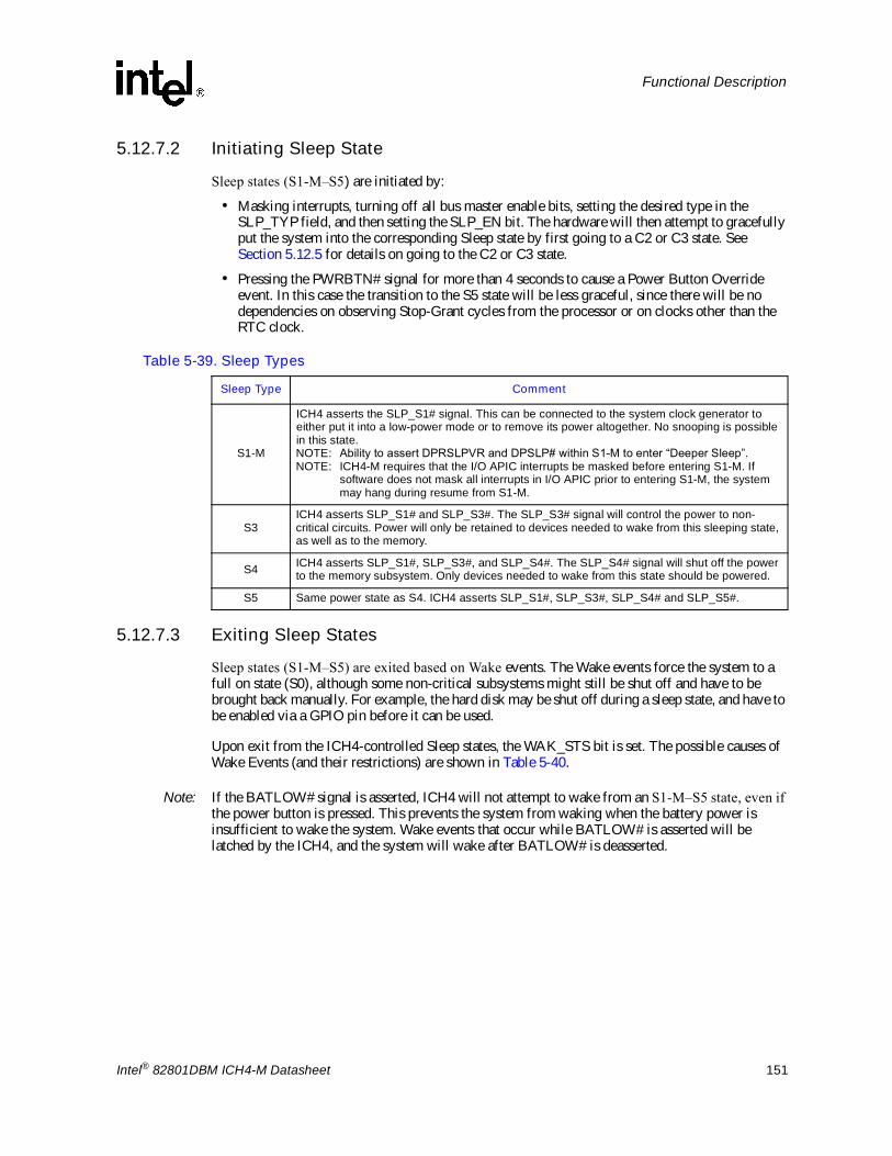
Intel® 82801DBM ICH4-M Datasheet 151
Functional Description
5.12.7.2 Initiating Sleep State
Sleep states (S1-M�S5) are initiated by:
� Masking interrupts, turning off all bus master enable bits, setting the desired type in the SLP_TYP field, and then setting the SLP_EN bit. The hardware will then attempt to gracefully put the system into the corresponding Sleep state by first going to a C2 or C3 state. See Section 5.12.5 for details on going to the C2 or C3 state.
� Pressing the PWRBTN# signal for more than 4 seconds to cause a Power Button Override event. In this case the transition to the S5 state will be less graceful, since there will be no dependencies on observing Stop-Grant cycles from the processor or on clocks other than the RTC clock.
5.12.7.3 Exiting Sleep States
Sleep states (S1-M�S5) are exited based on Wake events. The Wake events force the system to a full on state (S0), although some non-critical subsystems might still be shut off and have to be brought back manually. For example, the hard disk may be shut off during a sleep state, and have to be enabled via a GPIO pin before it can be used.
Upon exit from the ICH4-controlled Sleep states, the WAK_STS bit is set. The possible causes of Wake Events (and their restrictions) are shown in Table 5-40.
Note: If the BATLOW# signal is asserted, ICH4 will not attempt to wake from an S1-M�S5 state, even if the power button is pressed. This prevents the system from waking when the battery power is insufficient to wake the system. Wake events that occur while BATLOW# is asserted will be latched by the ICH4, and the system will wake after BATLOW# is deasserted.
Table 5-39. Sleep Types
Sleep Type Comment
S1-M
ICH4 asserts the SLP_S1# signal. This can be connected to the system clock generator to either put it into a low-power mode or to remove its power altogether. No snooping is possible in this state.NOTE: Ability to assert DPRSLPVR and DPSLP# within S1-M to enter �Deeper Sleep�.NOTE: ICH4-M requires that the I/O APIC interrupts be masked before entering S1-M. If
software does not mask all interrupts in I/O APIC prior to entering S1-M, the system may hang during resume from S1-M.
S3ICH4 asserts SLP_S1# and SLP_S3#. The SLP_S3# signal will control the power to non-critical circuits. Power will only be retained to devices needed to wake from this sleeping state, as well as to the memory.
S4 ICH4 asserts SLP_S1#, SLP_S3#, and SLP_S4#. The SLP_S4# signal will shut off the power to the memory subsystem. Only devices needed to wake from this state should be powered.
S5 Same power state as S4. ICH4 asserts SLP_S1#, SLP_S3#, SLP_S4# and SLP_S5#.

152 Intel® 82801DBM ICH4-M Datasheet
Functional Description
NOTES:1. This will be a wake event from S5 only if the sleep state was entered by setting the SLP_EN and SLP_TYP
bits via software.2. If in the S5 state due to a powerbutton override, the possible wake events are due to Power Button, Hard
Reset Without Cycling (See Command Type 3 in Table 5-95), and Hard Reset System (See Command Type 4 in Table 5-95).
3. The entry for USB changes from being able to wake from S1-M�S4 to being able to wake from S1-M�S5. Previous designs actively blocked wake events while in S5. There is no need to do this as software already disables waking from USB on S5 (so the wake bits are masked), and in the future power buttons will move to USB keyboards, and a wake from S5 will be necessary.
It is important to understand that the various GPIs have different levels of functionality when used as wake events. The GPIs that reside in the core power well can only generate wake events from an S1-M state. Also only certain GPIs are �ACPI Compliant,� meaning that their Status and Enable bits reside in ACPI I/O space. Table 5-41 summarizes the use of GPIs as wake events.
The latency to exit the various Sleep states varies greatly and is heavily dependent on power supply design, so much so that the exit latencies due to the ICH4 are insignificant.
Table 5-40. Causes of Wake Events
Cause States Can Wake From How Enabled
RTC Alarm S1-M�S5 (1) Set RTC_EN bit in PM1_EN register
Power Button S1-M�S5 Always enabled as Wake event
GPI[0:n] S1-M�S5 (1) GPE0_EN register
USB S1-M�S5 (3) Set USB1_EN, USB 2_EN and USB3_EN bits in GPE0_EN register
LAN S1-M�S5 Will use PME#. Wake enable set with LAN logic.
RI# S1-M�S5 (1) Set RI_EN bit in GPE0_EN register
AC �97 S1-M�S5 Set AC �97_EN bit in GPE0_EN register
Primary PME# S1-M�S5 PME_B0_EN bit in GPE0_EN register
Secondary PME# S1-M�S5 (1) Set PME_EN bit in GPE0_EN Register.
GST Timeout S1-M Setting the GST Timeout range to a value other than 00h.
SMBALERT# S1-M�S5 Always enabled as Wake event
SMBus Slave Message S1-M�S5
Wake/SMI# command always enabled as a Wake Event.NOTE: SMBus Slave Message can wake the system from
S1-M�S5, as well as from S5 due to Power Button Override.
SMBus Host Notify message received S1-M�S5 HOST_NOTIFY_WKEN bit SMBus Slave Command register.
Reported in the SMB_WAK_STS bit in the GPEO_STS register.
PME_B0 (internal USB EHCI controller) S1-M�S5 (1) Set PME_B0_EN bit in GPE0_EN register.
Table 5-41. GPI Wake Events
GPI Power Well Wake From Notes
GPI[7:0] Core S1-M
GPI[13:11], GPI[8] Resume S1-M�S5 ACPI Compliant

Intel® 82801DBM ICH4-M Datasheet 153
Functional Description
5.12.7.4 Sx-G3-Sx, Handling Power Failures
A power failure in a mobile system is a rare event, since the power subsystem should provide sufficient warning when the batteries are low. However, if the user removes the battery or leaves the system in an STR state for too long, a power failure could occur.
In either case, PWROK and RSMRST# are assumed to go low.
Depending on when the power failure occurs and how the system is designed, different transitions could occur due to a power failure.
The AFTER_G3 bit provides the ability to program whether or not the system should boot once power returns after a power loss event. If the policy is to not boot, the system will remain in an S5 state (unless previously in S4). There are only three possible events that will wake the system after a power failure.
1. PWRBTN#: PWRBTN# is always enabled as a wake event. When RSMRST# is low (G3 state), the PWRBTN_STS bit is reset. When the ICH4 exits G3 after power returns (RSMRST# goes high), the PWRBTN# signal is already high (because VCC-standby goes high before RSMRST# goes high) and the PWRBTN_STS bit is 0.
2. RI#: RI# does not have an internal pull-up. Therefore, if this signal is enabled as a wake event, it is important to keep this signal powered during the power loss event. If this signal goes low (active), when power returns, the RI_STS bit will be set and the system will interpret that as a wake event.
3. RTC Alarm: The RTC_EN bit is in the RTC well and is preserved after a power loss. Like PWRBTN_STS, the RTC_STS bit is cleared when RSMRST# goes low.
The ICH4 monitors both PWROK and RSMRST# to detect for power failures. If PWROK goes low, the PWROK_FLR bit is set. If RSMRST# goes low, PWR_FLR is set.
Note: Although PME_EN is in the RTC well, this signal cannot wake the system after a power loss. PME_EN is cleared by RTCRST# and PME_STS is cleared by RSMRST#.
Table 5-42. Transitions Due to Power Failure
State at Power Failure AFTERG3_EN bit Transition When Power Returns
S0, S1-M, S3 10
S5S0
S4 10
S4S0
S5 10
S5S0
154 Intel® 82801DBM ICH4-M Datasheet
Functional Description
5.12.8 Thermal ManagementThe ICH4 has mechanisms to assist with managing thermal problems in the system.
5.12.8.1 THRM# Signal
The THRM# signal is used as a status input for a thermal sensor. Based on the THRM# signal going active, the ICH4 generates an SMI# or SCI (depending on SCI_EN).
If the THRM_POL bit is set low, when the THRM# signal goes low, the THRM_STS bit will be set. This is an indicator that the thermal threshold has been exceeded. If the THRM_EN bit is set, then when THRM_STS goes active, either an SMI# or SCI is generated (depending on the SCI_EN bit being set).
The power management software (BIOS or ACPI) can then take measures to start reducing the temperature. Examples include shutting off unwanted subsystems, or halting the processor.
By setting the THRM_POL bit to high, another SMI# or SCI can optionally be generated when the THRM# signal goes back high. This allows the software (BIOS or ACPI) to turn off the cooling methods.
Note: THRM# assertion does not cause a TCO event message in S1-M, S3, or S4. The level of the signal will not be reported in the heartbeat message.
5.12.8.2 THRM# Initiated Passive Cooling
If the THRM# signal remains active for some time greater than 2 seconds and the ICH4 is in the S0/G0/C0 state, then the ICH4 enters an auto-throttling mode in which it provides a duty cycle on the STPCLK# signal. This reduces the overall power consumption by the system and should cool the system. The intended result of the cooling is that the THRM# signal should go back inactive.
For all programmed values (001�111), THRM# going active results in STPCLK# active for a minimum time of 12.5% and a maximum of 87.5%. The period is 1024 PCI clocks. Thus, the STPCLK# signal can be active for as little as 128 PCI clocks or as much as 896 PCI clocks. The actual slowdown (and cooling) of the processor depends on the instruction stream, because the processor is allowed to finish the current instruction. Furthermore, the ICH4 waits for the STOP-GRANT cycle before starting the count of the time the STPCLK# signal is active.
When THRM# goes inactive, the throttling will stop. In case the ICH4 is already attempting throttling because the THTL_EN bit is set, the duty cycle associated with the THRM# signal will have higher priority. If the ICH4 is in the C2, C3, or S1-M�S5 states, then no throttling will be caused by the THRM# signal being active.
5.12.8.3 THRM# Override Software Bit
The FORCE_THTL bit allows the BIOS to force passive cooling, just as if the THRM# signal had been active for 2 seconds. If this bit is set, the ICH4 starts throttling using the ratio in the THRM_DTY field.
When this bit is cleared, the ICH4 stops throttling, unless the THRM# signal has been active for 2 seconds or if the THTL_EN bit is set (indicating that ACPI software is attempting throttling).

Intel® 82801DBM ICH4-M Datasheet 155
Functional Description
5.12.8.4 Processor-Initiated Passive Cooling (Via Programmed Duty Cycle on STPCLK#)
Using the THTL_EN and THTL_DTY bits, the ICH4 can force a programmed duty cycle on the STPCLK# signal. This reduces the effective instruction rate of the processor and cut its power consumption and heat generation.
5.12.8.5 Active Cooling
Active cooling involves fans. The GPIO signals from the ICH4 can be used to turn on/off a fan.
5.12.9 Intel® SpeedStep® Technology ProtocolThe Intel® SpeedStep® technology feature enables a mobile system to operate in multiple processor performance/thermal states and to transition smoothly between them. The internal processor clock setting and processor supply voltage setting determine these states. The ICH4 supports a low-power mode and a high-performance mode.
Figure 5-14. Intel® SpeedStep® Technology Block Diagram
ICH4
CPUPERF#
CPUPWRGD
STPCLK #
PWROK
VGATE
From MainPower Supply
VddCore
SSMUXSEL
Mux
5
5High Voltage
Low Voltage
5VRCODE[4:0]
Intel®SpeedStep®
TechnologyEnabled Mobile
Processor
ProcessorVoltage
RegulatorModule (VRM)

156 Intel® 82801DBM ICH4-M Datasheet
Functional Description
5.12.9.1 Intel SpeedStep Technology Processor Requirements
Processors without Intel SpeedStep technology use the A20M#, IGNNE#, NMI and INTR input signals to determine the multiplier used by the processor�s PLL for the internal clock. With Intel SpeedStep technology processors, two multiplier values (one for the Maximum Performance state, a second for the Low Power-Battery Optimized state) are hard-wired within the processor. The ICH4 CPUPERF signal is used to select the processor state, based on ICH4 control logic.
The operating bus ratio must be available to the programmer, and is therefore suggested that it be read in a processor MSR. Also, the processor must return an indication that it is Intel SpeedStep technology enabled, which should be in the form of a status bit in a processor MSR or in the CPUID register.
The ICH4 is not capable of determining whether it is attached to a processor with or without Intel SpeedStep technology. When used a processor without Intel SpeedStep technology, software should not write or read the ICH4 Intel SpeedStep technology registers.
5.12.9.2 Intel SpeedStep Technology States
The ICH4 supports two system-level performance states: low-power mode and high-performance mode. Processor states are defined by valid combinations of core voltage levels and core clock speeds. These processor states can be used to alter the processor and system performance to conform to conditions of power and environment.
The low-power mode is used primarily when the system is powered from the battery, with the purpose being to maximize battery life. Mobile system performance is limited by thermal design and battery capacity. To improve thermal capacity, active cooling solutions such as a fan can be used, in addition to a passive cooling solution.
The high-performance mode assume that the mobile system is powered from an external AC/DC source. The purpose of this state is to maximize performance subject to thermal constraints. The ICH4 does not implement any restrictions on entry into high-performance mode. It will unconditionally transition into high-performance mode upon software command.
5.12.9.3 Voltage Regulator Interface
The voltage regulator interface is critical to the Intel SpeedStep technology concept. The power dissipation of the processor is proportional to the internal clock speed and to the square of the core supply voltage. As the internal clock speed of the processor changes, the minimum required core voltage supply level also changes. The interface signals are designed to allow the voltage regulator to change settings without causing a power-on reset.
� VRCODE[4:0] is a 5-bit input to the Voltage Regulator. These signals are not outputs from the ICH4, but instead are outputs from an external mux. Future voltage regulators may integrate this mux.
� The SSMUXSEL signal is an ICH4 output. It can be used directly can control the external mux that selects the high or low values for VRCODE[4:0].
� VRON (aka PWROK from main power supply) is an input to the regulator, and when VRON is asserted the regulator turns on and settles to the output defined by VRCODE[4:0].
VGATE is an input from the regulator indicating that all of the outputs from the regulator are on and within specification. When the system is transitioning between performance states, the voltage regulator output may be required to change. It is not desirable, however, that CPUPWRGOOD

Intel® 82801DBM ICH4-M Datasheet 157
Functional Description
becomes deasserted during these transitions. Normally, this would indicate to the system electronics that a power-on reset be performed, which would invalidate the system context. ICH4 prevents this from occurring by maintaining CPUPWRGOOD during the transition. CPUPWRGOOD must also be maintained during an S1-M state.
5.12.10 Event Input Signals and Their UsageThe ICH4 has various input signals that trigger specific events. This section describes those signals and how they should be used.
5.12.10.1 PWRBTN# - Power ButtonThe ICH4 PWRBTN# signal operates as a �Fixed Power Button� as described in the ACPI specification. PWRBTN# signal has a 16 ms de-bounce on the input. The state transition descriptions are included in Table 5-43. Note that the transitions start as soon as the PWRBTN# is pressed (but after the debounce logic), and does not depend on when the Power Button is released.
Power Button Override Function
If PWRBTN# is observed active for at least four consecutive seconds, then the state machine should unconditionally transition to the G2/S5 state, regardless of present state (S0�S4). In this case, the transition to the G2/S5 state should not depend on any particular response from the processor (e.g., a Stop-Grant cycle), nor any similar dependency from any other subsystem.
New: A power button override will force a transition to S5, even if PWROK is not active.
The PWRBTN# status is readable to check if the button is currently being pressed or has been released. The status is taken after the de-bounce, and is readable via the PWRBTN_LVL bit.
Note: The 4-second PWRBTN# assertion should only be used if a system lock-up has occurred. The 4-second timer starts counting when the ICH4 is in a S0 state. If the PWRBTN# signal is asserted and held active when the system is in a suspend state (S1-M�S5), the assertion causes a wake event. Once the system has resumed to the S0 state, the 4-second timer starts.
Table 5-43. Transitions Due to Power Button
Present State Event Transition/Action Comment
S0/Cx PWRBTN# goes low SMI# or SCI generated (depending on SCI_EN)
Software will typically initiate a Sleep state.
S1-M�S5 PWRBTN# goes low Wake Event. Transitions to S0 state. Standard wakeup
G3 PWRBTN# pressed NoneNo effect since no power.Not latched nor detected.
S0�S4PWRBTN# held low for at least 4 consecutive
seconds
Unconditional transition to S5 state.
No dependence on processor (e.g., Stop-Grant cycles) or any other subsystem.
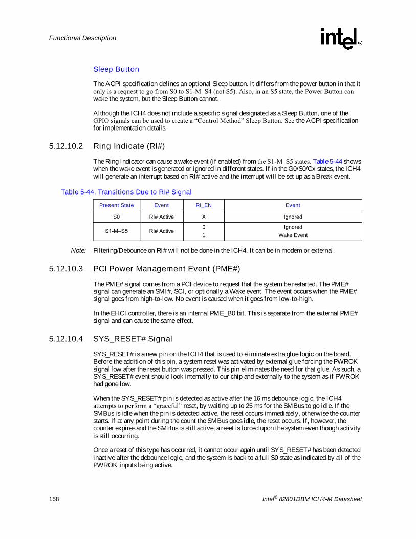
158 Intel® 82801DBM ICH4-M Datasheet
Functional Description
Sleep Button
The ACPI specification defines an optional Sleep button. It differs from the power button in that it only is a request to go from S0 to S1-M�S4 (not S5). Also, in an S5 state, the Power Button can wake the system, but the Sleep Button cannot.
Although the ICH4 does not include a specific signal designated as a Sleep Button, one of the GPIO signals can be used to create a �Control Method� Sleep Button. See the ACPI specification for implementation details.
5.12.10.2 Ring Indicate (RI#)
The Ring Indicator can cause a wake event (if enabled) from the S1-M�S5 states. Table 5-44 shows when the wake event is generated or ignored in different states. If in the G0/S0/Cx states, the ICH4 will generate an interrupt based on RI# active and the interrupt will be set up as a Break event.
Note: Filtering/Debounce on RI# will not be done in the ICH4. It can be in modem or external.
5.12.10.3 PCI Power Management Event (PME#)
The PME# signal comes from a PCI device to request that the system be restarted. The PME# signal can generate an SMI#, SCI, or optionally a Wake event. The event occurs when the PME# signal goes from high-to-low. No event is caused when it goes from low-to-high.
In the EHCI controller, there is an internal PME_B0 bit. This is separate from the external PME# signal and can cause the same effect.
5.12.10.4 SYS_RESET# Signal
SYS_RESET# is a new pin on the ICH4 that is used to eliminate extra glue logic on the board. Before the addition of this pin, a system reset was activated by external glue forcing the PWROK signal low after the reset button was pressed. This pin eliminates the need for that glue. As such, a SYS_RESET# event should look internally to our chip and externally to the system as if PWROK had gone low.
When the SYS_RESET# pin is detected as active after the 16 ms debounce logic, the ICH4 attempts to perform a �graceful� reset, by waiting up to 25 ms for the SMBus to go idle. If the SMBus is idle when the pin is detected active, the reset occurs immediately, otherwise the counter starts. If at any point during the count the SMBus goes idle, the reset occurs. If, however, the counter expires and the SMBus is still active, a reset is forced upon the system even though activity is still occurring.
Once a reset of this type has occurred, it cannot occur again until SYS_RESET# has been detected inactive after the debounce logic, and the system is back to a full S0 state as indicated by all of the PWROK inputs being active.
Table 5-44. Transitions Due to RI# Signal
Present State Event RI_EN Event
S0 RI# Active X Ignored
S1-M�S5 RI# Active01
IgnoredWake Event
Intel® 82801DBM ICH4-M Datasheet 159
Functional Description
5.12.10.5 THRMTRIP# Signal
If THRMTRIP# goes active, the processor is indicating an overheat condition, and the ICH4 immediately transitions to an S5 state. However, since the processor has overheated, it does not respond to the ICH4�s STPCLK# pin with a stop grant special cycle. Therefore, the ICH4 does not wait for one. Immediately upon seeing THRMTRIP# low, the ICH4 initiates a transition to the S5 state, drives SLP_S3#, SLP_S4#, SLP_S5# low, and sets the CTS bit. The transition looks like a power button override.
It is extremely important that when a THRMTRIP# event occurs, the ICH4 power down immediately without following the normal S0 -> S5 path. This path may be taken in parallel, but ICH4 must immediately enter a power down state. It will do this by driving SLP_S3#, SLP_S4#, and SLP_S5# immediately after sampling THRMTRIP# active.
If the processor is running extremely hot and is heating up, it is possible (although very unlikely) that components around it (e.g., the ICH4, are no longer executing cycles properly). Therefore, if THRMTRIP# fires, and the ICH4 is relying on state machine logic to perform the power down, the state machine may not be working, and the system will not power down.
The ICH4 follows this flow for THRMTRIP#.
1. At boot (PCIRST# low), THRMTRIP# ignored.
2. After power-up (PCIRST# high), if THRMTRIP# sampled active, SLP_S3#, SLP_S4#, and SLP_S5# fire, and normal sequence of sleep machine starts.
3. Until sleep machine enters the S5 state, SLP_S3#, SLP_S4#, and SLP_S5# stay active, even if THRMTRIP# is now inactive. This is the equivalent of �latching� the thermal trip event.
4. If S5 state reached, go to step #1, otherwise stay here. If the ICH4 never reaches S5, ICH4 will not reboot until power is cycled.
Note: A CPU Thermal trip event will set AFTERG3_EN bit, clear the PWRBTN_STS bit, clear the GPE0_EN & GPE1_EN register bits, and clear the SMB_WAK_STS bit only if SMB_WAK_STS was set due to SMBus slave receiving message and not set due to SMBAlert. Refer to AFTERG3_EN bit description in Section 9.8.1.3 - GEN_PMCON_3 Register for more details.
5.12.10.6 AGPBUSY#
The AGPBUSY# signal is an input from the AGP graphics component to indicate if it is busy. If prior to going to the C3 state the AGPBUSY# signal is active, the BM_STS bit is set. If after going to the C3 state, the AGPBUSY# signal goes back active, the ICH4 treats this as if one of the PCI REQ# signals went active. This is treated as a break event.
5.12.11 ALT Access ModeBefore entering a low power state, several registers from powered down parts may need to be saved. In the majority of cases, this is not an issue, as registers have read and write paths. However, several of the ISA compatible registers are either read only or write only. To get data out of write-only registers, and to restore data into read-only registers, the ICH4 implements an ALT access mode.
If the ALT access mode is entered and exited after reading the registers of the ICH4 timer (8254), the timer starts counting faster (13.5 ms). The following steps listed below can cause problems:
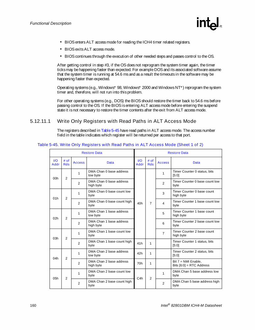
160 Intel® 82801DBM ICH4-M Datasheet
Functional Description
� BIOS enters ALT access mode for reading the ICH4 timer related registers.
� BIOS exits ALT access mode.
� BIOS continues through the execution of other needed steps and passes control to the OS.
After getting control in step #3, if the OS does not reprogram the system timer again, the timer ticks may be happening faster than expected. For example DOS and its associated software assume that the system timer is running at 54.6 ms and as a result the timeouts in the software may be happening faster than expected.
Operating systems (e.g., Windows* 98, Windows* 2000 and Windows NT*) reprogram the system timer and, therefore, will not run into this problem.
For other operating systems (e.g., DOS) the BIOS should restore the timer back to 54.6 ms before passing control to the OS. If the BIOS is entering ALT access mode before entering the suspend state it is not necessary to restore the timer contents after the exit from ALT access mode.
5.12.11.1 Write Only Registers with Read Paths in ALT Access Mode
The registers described in Table 5-45 have read paths in ALT access mode. The access number field in the table indicates which register will be returned per access to that port.
Table 5-45. Write Only Registers with Read Paths in ALT Access Mode (Sheet 1 of 2)
Restore Data Restore Data
I/OAddr
# ofRds Access Data I/O
Addr# ofRds Access Data
00h 21 DMA Chan 0 base address
low byte
40h 7
1 Timer Counter 0 status, bits [5:0]
2 DMA Chan 0 base address high byte 2 Timer Counter 0 base count low
byte
01h 21 DMA Chan 0 base count low
byte 3 Timer Counter 0 base count high byte
2 DMA Chan 0 base count high byte 4 Timer Counter 1 base count low
byte
02h 21 DMA Chan 1 base address
low byte 5 Timer Counter 1 base count high byte
2 DMA Chan 1 base address high byte 6 Timer Counter 2 base count low
byte
03h 21 DMA Chan 1 base count low
byte 7 Timer Counter 2 base count high byte
2 DMA Chan 1 base count high byte 41h 1 Timer Counter 1 status, bits
[5:0]
04h 21 DMA Chan 2 base address
low byte 42h 1 Timer Counter 2 status, bits [5:0]
2 DMA Chan 2 base address high byte 70h 1 Bit 7 = NMI Enable,
Bits [6:0] = RTC Address
05h 21 DMA Chan 2 base count low
byteC4h 2
1 DMA Chan 5 base address low byte
2 DMA Chan 2 base count high byte 2 DMA Chan 5 base address high
byte

Intel® 82801DBM ICH4-M Datasheet 161
Functional Description
NOTES:1. The OCW1 register must be read before entering ALT access mode.2. Bits 5, 3, 1, and 0 return 0.
06h 21 DMA Chan 3 base address
low byteC6h 2
1 DMA Chan 5 base count low byte
2 DMA Chan 3 base address high byte 2 DMA Chan 5 base count high
byte
07h 21 DMA Chan 3 base count low
byteC8h 2
1 DMA Chan 6 base address low byte
2 DMA Chan 3 base count high byte 2 DMA Chan 6 base address high
byte
08h 6
1 DMA Chan 0�3 Command2
CAh 21 DMA Chan 6 base count low
byte
2 DMA Chan 0�3 Request 2 DMA Chan 6 base count high byte
3 DMA Chan 0 Mode: Bits(1:0) = �00�
CCh 21 DMA Chan 7 base address low
byte
4 DMA Chan 1 Mode: Bits(1:0) = �01� 2 DMA Chan 7 base address high
byte
5 DMA Chan 2 Mode: Bits(1:0) = �10�
CEh 21 DMA Chan 7 base count low
byte
6 DMA Chan 3 Mode: Bits(1:0) = �11�. 2 DMA Chan 7 base count high
byte
20h 12
1 PIC ICW2 of Master controller
D0h 6
1 DMA Chan 4�7 Command2
2 PIC ICW3 of Master controller 2 DMA Chan 4�7 Request
3 PIC ICW4 of Master controller 3 DMA Chan 4 Mode: Bits(1:0) = 00
4 PIC OCW1 of Master controller1 4 DMA Chan 5 Mode: Bits(1:0) =
01
5 PIC OCW2 of Master controller 5 DMA Chan 6 Mode: Bits(1:0) =
10
6 PIC OCW3 of Master controller 6 DMA Chan 7 Mode: Bits(1:0) =
11.
7 PIC ICW2 of Slave controller
8 PIC ICW3 of Slave controller
9 PIC ICW4 of Slave controller
10 PIC OCW1 of Slave controller1
11 PIC OCW2 of Slave controller
12 PIC OCW3 of Slave controller
Table 5-45. Write Only Registers with Read Paths in ALT Access Mode (Sheet 2 of 2)
Restore Data Restore Data
I/OAddr
# ofRds Access Data I/O
Addr# ofRds Access Data

162 Intel® 82801DBM ICH4-M Datasheet
Functional Description
5.12.11.2 PIC Reserved Bits
Many bits within the PIC are reserved, and must have certain values written in order for the PIC to operate properly. Therefore, there is no need to return these values in ALT access mode. When reading PIC registers from 20h and A0h, the reserved bits shall return the values listed in Table 5-46.
Table 5-46. PIC Reserved Bits Return Values
PIC Reserved Bits Value Returned
ICW2[2:0] 000ICW4[7:5] 000ICW4[3:2] 00ICW4[0] 0
OCW2[4:3] 00OCW3[7] 0OCW3[5] Reflects bit 6
OCW3[4:3] 01

Intel® 82801DBM ICH4-M Datasheet 163
Functional Description
5.12.11.3 Read Only Registers with Write Paths in ALT Access ModeThe registers described in Table 5-47 have write paths to them in ALT access mode. Software restores these values after returning from a powered down state. These registers must be handled special by software. When in normal mode, writing to the base address/count register also writes to the current address/count register. Therefore, the base address/count must be written first, then the part is put into ALT access mode and the current address/count register is written.
5.12.12 System Power Supplies, Planes, and Signals
5.12.12.1 Power Plane Control with SLP_S3#, SLP_S4# and SLP_S5#
The SLP_S3# output signal can be used to cut power to the system core supply, since it only goes active for the STR state (typically mapped to ACPI S3). Power must be maintained to the ICH4 resume well, and to any other circuits that need to generate Wake signals from the STR state.
Cutting power to the core may be done via the power supply, or by external FETs to the motherboard. The SLP_S4# or SLP_S5# output signal can be used to cut power to the system core supply, as well as power to the system memory, since the context of the system is saved on the disk. Cutting power to the memory may be done via the power supply, or by external FETs to the motherboard.
5.12.12.2 SLP_S1# SignalThe SLP_S1# signal will typically use this signal to cut power to non-critical subsystems while in the S1-M state.
5.12.12.3 PWROK SignalThe PWROK input should go active based on the core supply voltages becoming valid. PWROK should go active no sooner than 10 ms after Vcc3_3 and Vcc1_5 have reached their nominal values.
Note:
1. Traditional designs have a reset button logically ANDs with the PWROK signal from the power supply and the processor�s voltage regulator module. If this is done with the ICH4, the PWROK_FLR bit will be set. The ICH4 treats this internally as if the RSMRST# signal had gone active. However, it is not treated as a full power failure. If PWROK goes inactive and then active (but RSMRST# stays high), then the ICH4 will reboot (regardless of the state of the AFTERG3 bit). If the RSMRST# signal also goes low before PWROK goes high, then this is a full power failure, and the reboot policy is controlled by the AFTERG3 bit.
2. PWROK and RSMRST# are sampled using the RTC clock. Therefore, low times that are less than one RTC clock period may not be detected by the ICH4.
3. In the case of true PWROK failure, PWROK will go low first before the VRMPWRGD/VGATE.
Table 5-47. Register Write Accesses in ALT Access Mode
I/O Address Register Write Value
08h DMA Status Register for channels 0�3.
D0h DMA Status Register for channels 4�7.

164 Intel® 82801DBM ICH4-M Datasheet
Functional Description
5.12.12.4 VRMPWRGD Signal
This signal is connected to the processor�s VRM and is internally AND�d with the PWROK signal that comes from the system power supply. This saves the external AND gate found in desktop systems.
5.12.12.5 VGATE Signal
VGATE is an input from the regulator indicating that all of the outputs from the regulator are on and within specification. When the system is performing an Intel SpeedStep transition between performance states, the voltage regulator output may be required to change. It is not desirable, however, that CPUPWRGD becomes deasserted during these transitions. Normally, this would indicate to the system that a power-on reset be performed, which would invalidate the system context. Intel ICH4 prevents this from occurring by maintaining CPUPWRGOOD during the transition. CPUPWRGOOD must also be maintained during an S1-M state.
5.12.12.6 BATLOW# - Battery Low
The BATLOW# input can inhibit waking from a sleep state if there is not sufficient power. It will also cause an SMI# if the system is already in an S0 state.
5.12.12.7 Controlling Leakage and Power Consumption during Low-Power States
To control leakage in the system, various signals tri-state or go low during some low-power states.
General principles:
� All signals going to powered down planes (either internally or externally) must be either tri-stated or driven low.
� Signals with pull-up resistors should not be low during low-power states. This is to avoid the power consumed in the pull-up resistor.
� Buses should be halted (and held) in a known state to avoid a floating input (perhaps to some other device). Floating inputs can cause extra power consumption.
Based on the above principles, the following measures are taken:
� During S3 (STR), all signals attached to powered down planes will be tri-stated or driven low.

Intel® 82801DBM ICH4-M Datasheet 165
Functional Description
5.12.13 Clock GeneratorsThe clock generator is expected to provide the frequencies shown in Table 5-48.
5.12.13.1 Clock Control Signals from ICH4 to Clock Synthesizer
The clock generator is assumed to have direct connect from the following ICH4 signals:
� STP_CPU#: Stops processor clocks in C3 state
� STP_PCI#: Stops system PCI clocks (not the ICH4 free-running 33 MHz clock) due to CLKRUN# protocol
� SLP_S1#: Stops all clocks in S1-M
Table 5-48. Intel ICH4 Clock Inputs
Clock Domain Frequency Source Usage
CLK66 66 MHz Main Clock Generator
Should be running in all Cx states. Stopped in S1-M based on SLP_S1# assertion. Stopped in S3 ~ S5 based on SLP_S3# assertion.
PCICLK 33 MHz Main Clock Generator
Free-running (not affected by STP_PCI# PCI Clock to ICH4. This is not the system PCI clock. This clock must keep running in S0 while the system PCI clock may stop based on CLKRUN# protocol. This clock is stopped in S1-M based on SLP_S1# assertion. Stopped in S3 ~ S5 based on SLP_S3# assertion.
CLK48 48 MHz Main Clock Generator
Used by USB Controllers. This clock is stopped in S1-M based on SLP_S1# assertion. Stopped in S3 ~ S5 based on SLP_S3# assertion.
CLK14 14.318 MHz Main Clock Generator
Used by ACPI timers. This clock is stopped in S1-M based on SLP_S1# assertion. Stopped in S3 ~ S5 based on SLP_S3# assertion.
AC_BIT_CLK 12.288 MHz AC �97 Codec AC �97 Link. Control policy is determined by the clock source.
APICCLK 16.67 MHzor 33 MHz
Main Clock Generator
Used for ICH4-processor interrupt messages. Should be running in C0, C1 and C2. Stopped in C3 based on STP_CPU# assertion. Stopped in S1-M based on SLP_S1# assertion. Stopped in S3 ~ S5 based on SLP_S3# assertion.
LAN_CLK 0.8 to 50 MHz
LAN Connect
LAN Connect link. Control policy is determined by the clock source.

166 Intel® 82801DBM ICH4-M Datasheet
Functional Description
5.12.14 Legacy Power Management Theory of OperationInstead of relying on ACPI software, legacy power management uses BIOS and various hardware mechanisms. ICH4 has a greatly simplified method for legacy power management compared with previous generations (e.g., the PIIX4).
The scheme relies on the concept of detecting when individual subsystems are idle, detecting when the whole system is idle, and detecting when accesses are attempted to idle subsystems.
However, the OS is assumed to be at least APM enabled. Without APM calls, there is no quick way to know when the system is idle between keystrokes. The ICH4 does not support the burst modes found in previous components (e.g., the PIIX4).
5.12.14.1 APM Power Management
There are additional requirements associated with device power management. To handle this, the ICH4 has specific SMI# traps available. The following algorithm is used:
1. The periodic SMI# timer checks if a device is idle for the require time. If so, it puts to the device into a low-power states and sets the associated SMI# trap.
2. When software (not the SMI# handler) attempts to access the device, a trap occurs (the cycle does not really go to the device and an SMI# is generated).
3. The SMI# handler turns on the device and turns off the trap
The SMI# handler exits with an I/O restart. This allows the original software to continue.

Intel® 82801DBM ICH4-M Datasheet 167
Functional Description
5.13 System Management (D31:F0)The ICH4 provides various functions to make a system easier to manage and to lower the Total Cost of Ownership (TCO) of the system. Features and functions can be augmented via external A/D converters and GPIO, as well as an external microcontroller.
The following features and functions are supported by the ICH4:
� Processor present detection
� Detects if processor fails to fetch the first instruction after reset
� Various Error detection (e.g., ECC Errors) Indicated by Host Controller
� Can generate SMI#, SCI, SERR, NMI, or TCO interrupt
� Intruder Detect input
� Can generate TCO interrupt or SMI# when the system cover is remove
� INTRUDER# allowed to go active in any power state, including G3
� Detection of bad FWH programming
� Detects if data on first read is FFh (indicates unprogrammed FWH)
� Ability to hide a PCI device
� Allows software to hide a PCI device in terms of configuration space through the use of a device hide register (See Section 8.1.26)
Note: Voltage ID from the processor can be read via GPI signals.
5.13.1 Theory of OperationThe System Management functions are designed to allow the system to diagnose failing subsystems. The intent of this logic is that some of the system management functionality be provided without the aid of an external microcontroller.
5.13.1.1 Detecting a System Lockup
When the processor is reset, it is expected to fetch its first instruction. If the processor fails to fetch the first instruction after reset, the TCO timer times out twice and the ICH4 asserts PCIRST#.
5.13.1.2 Handling an Intruder
The ICH4 has an input signal, INTRUDER#, that can be attached to a switch that is activated by the system�s case being open. This input has a two RTC clock debounce. If INTRUDER# goes active (after the debouncer), this will set the INTRD_DET bit in the TCO_STS register. The INTRD_SEL bits in the TCO_CNT register can enable the ICH4 to cause an SMI# or interrupt. The BIOS or interrupt handler can then cause a transition to the S5 state by writing to the SLP_EN bit.
The software can also directly read the status of the INTRUDER# signal (high or low) by clearing and then reading the INTRD_DET bit. This allows the signal to be used as a GPI if the intruder function is not required.
168 Intel® 82801DBM ICH4-M Datasheet
Functional Description
If the INTRUDER# signal goes inactive some point after the INTRD_DET bit is written as a 1, then the INTRD_DET signal will go to a 0 when INTRUDER# input signal goes inactive. Note that this is slightly different than a classic sticky bit, since most sticky bits would remain active indefinitely when the signal goes active and would immediately go inactive when a 1 is written to the bit.
Note: The INTRD_DET bit resides in the ICH4�s RTC well, and is set and cleared synchronously with the RTC clock. Thus, when software attempts to clear INTRD_DET (by writing a 1 to the bit location) there may be as much as two RTC clocks (about 65 µs) delay before the bit is actually cleared. Also, the INTRUDER# signal should be asserted for a minimum of 1 ms to guarantee that the INTRD_DET bit will be set.
Note: If the INTRUDER# signal is still active when software attempts to clear the INTRD_DET bit, the bit will remain set and the SMI will be generated again immediately. The SMI handler can clear the INTRD_SEL bits to avoid further SMIs. However, if the INTRUDER# signal goes inactive and then active again, there will not be further SMIs, since the INTRD_SEL bits would select that no SMI# be generated.
5.13.1.3 Detecting Improper FWH Programming
The ICH4 can detect the case where the FWH is not programmed. This results in the first instruction fetched to have a value of FFh. If this occurs, the ICH4 sets the BAD_BIOS bit, which can then be reported via the Heartbeat and Event reporting using an external, Alert on LAN enabled LAN Controller (See Section 5.13.2).
5.13.1.4 Handling an ECC Error or Other Memory Error
The Host Controller provides a message to indicate that it would like to cause an SMI#, SCI, SERR#, or NMI. The software must check the Host Controller as to the exact cause of the error.
5.13.2 Alert on LAN*The ICH4 integrated LAN controller supports Alert on LAN functionality when used with the 82562EM Platform LAN Connect component. This allows the integrated LAN controller to report messages to a network management console without the aid of the system processor. This is crucial in cases where the processor is malfunctioning or cannot function due to being in a low-power state.
The ICH4 also features an independent, dedicated SMBus interface, referred to as the SMLINK interface that can be used with an external Alert on LAN (or Alert on LAN 2) enabled LAN Controller. This separate interface is required, since devices on the system SMBus will be powered down during some low power states.
The basic scheme is for the ICH4 integrated LAN Controller to send a prepared Ethernet message to a network management console. The prepared message is stored in the non-volatile EEPROM that is connected to the ICH4.
Messages will be sent by the LAN Controller either because a specific event has occurred, or they will be sent periodically (also known as a heartbeat). The event and heartbeat messages have the exact same format. The event messages are sent based on events occurring. The heartbeat messages is sent every 30 to 32 seconds. When an event occurs, the ICH4 sends a new message and increments the SEQ[3:0] field. For heartbeat messages, the sequence number does not increment.

Intel® 82801DBM ICH4-M Datasheet 169
Functional Description
The following rules/steps apply if the system is in a G0 state and the policy is for the ICH4 to reboot the system after a hardware lockup:
1. Upon detecting the lockup the SECOND_TO_STS bit will be set. The ICH4 may send up to 1 Event message to the D110. The ICH4 then attempts to reboot the processor.
2. If the reboot at step 1 is successful, BIOS should clear the SECOND_TO_STS bit. This prevents any further Heartbeats from being sent. The BIOS may then perform addition recovery/boot steps. (See note 2.)
3. If the reboot attempt in step 1 is not successful, then the timer will timeout a third time. At this point the system has locked up and was unsuccessful in rebooting. The ICH4 does not attempt to automatically reboot again. The ICH4 starts sending a message every heartbeat period (30�32 seconds). The heartbeats continue until some external intervention occurs (reset, power failure, etc.).
4. After step 3 (unsuccessful reboot after third timeout), if the user does a Power Button Override, the system goes to an S5 state. The ICH4 continues sending the messages every heartbeat period.
5. After step 4 (power button override after unsuccessful reboot) if the user presses the Power Button again, the system should wake to an S0 state and the processor should start executing the BIOS.
6. If step 5 (power button press) is successful in waking the system, the ICH4 continues sending messages every heartbeat period until the BIOS clears the SECOND_TO_STS bit. (See note 2)
7. If step 5 (power button press) is unsuccessful in waking the system, the ICH4 continues sending a message every heartbeat period. The ICH4 does not attempt to automatically reboot again. The ICH4 will start sending a message every heartbeat period (30�32 seconds). The heartbeats continue until some external intervention occurs (reset, power failure, etc.). (See note 3)
8. After step 3 (unsuccessful reboot after third timeout), if a reset is attempted (using a button that pulses PWROK low or via the message on the SMBus slave interface), the ICH4 attempts to reset the system.
9. After step 8 (reset attempt) if the reset is successful, BIOS is run. The ICH4 continues sending a message every heartbeat period until the BIOS clears the SECOND_TO_STS bit. (See note 2)
10. After step 8 (reset attempt), if the reset is unsuccessful, then the ICH4 continues sending a message every heartbeat period. The ICH4 does not attempt to reboot the system again without external intervention. (See note 3)
The following rules/steps apply if the system is in a G0 state and the policy is for the ICH4 to not reboot the system after a hardware lockup.
1. Upon detecting the lockup the SECOND_TO_STS bit is set. The ICH4 sends a message with the Watchdog (WD) Event status bit set (and any other bits that must also be set). This message is sent as soon as the lockup is detected, and is sent with the next (incremented) sequence number.
2. After step 1, the ICH4 sends a message every heartbeat period until some external intervention occurs.
3. Rules/steps 4�10 apply if no user intervention (resets, power button presses, SMBus reset messages) occur after a third timeout of the watchdog timer. If the intervention occurs before the third timeout, then jump to rule/step11.
4. After step 3 (third timeout), if the user does a Power Button Override, the system goes to an S5 state. The ICH4 continues sending heartbeats at this point.

170 Intel® 82801DBM ICH4-M Datasheet
Functional Description
5. After step 4 (power button override), if the user presses the power button again, the system should wake to an S0 state and the processor should start executing the BIOS.
6. If step 5 (power button press) is successful in waking the system, the ICH4 continues sending heartbeats until the BIOS clears the SECOND_TO_STS bit. (See note 2)
7. If step 5 (power button press) is unsuccessful in waking the system, the ICH4 continues sending heartbeats. The ICH4 does not attempt to reboot the system again until some external intervention occurs (reset, power failure, etc.). (See note 3)
8. After step 3 (3rd timeout), if a reset is attempted (using a button that pulses PWROK low or via the message on the SMBus slave interface), the ICH4 attempts to reset the system.
9. If step 8 (reset attempt) is successful, then the BIOS will be run. The ICH4 continues sending heartbeats until the BIOS clears the SECOND_TO_STS bit. (See note 2)
10. If step 8 (reset attempt), is unsuccessful, the ICH4 continues sending heartbeats. The ICH4 does not attempt to reboot the system again without external intervention. Note: A system that has locked up and can not be restarted with power button press is probably broken (bad power supply, short circuit on some bus, etc.).
11. This and the following rules/steps apply if the user intervention (power button press, reset, SMBus message, etc.) occur prior to the third timeout of the watchdog timer.
12. After step 1 (second timeout), if the user does a Power Button Override, the system goes to an S5 state. The ICH4 continues sending heartbeats at this point.
13. After step 12 (power button override), if the user presses the power button again, the system should wake to an S0 state and the processor should start executing the BIOS.
14. If step 13 (power button press) is successful in waking the system, the ICH4 will continue sending heartbeats until the BIOS clears the SECOND_TO_STS bit. (See note 2)
15. If step 13 (power button press) is unsuccessful in waking the system, the ICH4 will continue sending heartbeats. The ICH4 will not attempt to reboot the system again until some external intervention occurs (reset, power failure, etc.). (See note 3)
16. After step 1 (second timeout), if a reset is attempted (using a button that pulses PWROK low or via the message on the SMBus slave interface), the ICH4 will attempt to reset the system.
17. If step 16 (reset attempt) is successful, then the BIOS will be run. The ICH4 will continue sending heartbeats until the BIOS clears the SECOND_TO_STS bit. (See note 2)
18. If step 16 (reset attempt), is unsuccessful, then the ICH4 will continue sending heartbeats. The ICH4 will not attempt to reboot the system again without external intervention. (See note 3)
If the system is in a G1 (S1-M�S4) state, the ICH4 will send a heartbeat message every 30�32 seconds. If an event occurs prior to the system being shutdown, the ICH4 will immediately send an event message with the next incremented sequence number. After the event message, the ICH4 will resume sending heartbeat messages.
Note: Notes for Previous two numbered lists.
1. Normally, the ICH4 does not send heartbeat messages while in the G0 state (except in the case of a lockup). However, if a hardware event (or heartbeat) occurs just as the system is transitioning into a G0 state, the hardware will continue to send the message even though the system will be in a G0 state (and the status bits may indicate this).
When used with an external Alert on LAN enabled LAN controller, the ICH4 sends these messages via the SMLINK signals. When sending messages via these signals, the ICH4 abides by the SMBus rules associated with collision detection. It delays starting a message until the bus is idle, and will detect collisions. If a collision is detected, the ICH4 waits until the bus is idle and tries again.

Intel® 82801DBM ICH4-M Datasheet 171
Functional Description
2. WARNING: It is important that the BIOS clears the SECOND_TO_STS bit, as the alerts will interfere with the LAN device driver from working properly. The alerts reset part of the D110 and would prevent an operating system�s device driver from sending or receiving some messages.
3. A system that has locked up and can not be restarted with power button press is assumed to have broken hardware (bad power supply, short circuit on some bus, etc.), and is beyond ICH4�s recovery mechanisms.
4. A spurious alert could occur in the following sequence:
� The processor has initiated an alert using the SEND_NOW bit.
� During the alert, the THRM#, INTRUDER# or GPI[11] changes state.
� The system then goes to a non-S0 state.
Once the system transitions to the non-S0 state, it may send a single alert with an incremental SEQUENCE number.
5. An inaccurate alert message can be generated in the following scenario.
� The system successfully boots after a second watchdog Timeout occurs.
� PWROK goes low (typically, due to a reset button press) or a power button override occurs (before the SECOND_TO_STS bit is cleared).
� An alert message indicating that the processor is missing or locked up is generated with a new sequence number.
Note: Section 5.13.2 describes the �Processor Missing Event Status� and how an Alert Message can be sent via LAN. This feature is meant to function when a processor is installed in the socket (but is non-functional) and was not intended to alert when the processor was not installed. When the processor is not installed, VRMPWRGD is programmed not to assert which prevents TCO timer operation. It is this timer that is used to set the SECOND_TO_STS bit in TCO2_STS (TCOBase+60h), used for the alert.
To enable this messaging without a processor installed in the socket, external logic, monitoring processor socket signal SKTOCC#, should drive VID:4] low which will enable the VRM to drive its CPUPWRGD signal, which in turn will allow the CPU Dead Alert to function under this empty socket condition.
Table 5-49 shows the data included in the Alert on LAN messages.
Table 5-49. Alert on LAN* Message Data
Field Comment
Cover Tamper Status 1 = This bit will be set if the intruder detect bit is set (INTRD_DET).
Temp Event Status 1 = This bit will be set if the ICH4 THERM# input signal is asserted.
Processor Missing Event Status 1 = This bit will be set if the processor failed to fetch the first instruction.
TCO Timer Event Status 1 = This bit is set when the TCO timer expires.
Software Event Status 1 = This bit is set when software writes a 1 to the SEND_NOW bit.
Unprogrammed FWH Event Status 1 = First BIOS fetch returned a value of FFh, indicating that the FWH has not yet been programmed (still erased).
GPIO Status1 = This bit is set when GPIO[11] signal is high.0 = This bit is cleared when GPIO[11] signal is low.An event message is triggered on an transition of GPIO[11].

172 Intel® 82801DBM ICH4-M Datasheet
Functional Description
SEQ[3:0]This is a sequence number. It is initially 0, and increments each time the ICH4 sends a new message. Upon reaching 1111, the sequence number rolls over to 0000. MSB (SEQ3) sent first.
System Power State 00 = G0, 01 = G1, 10 = G2, 11 = Pre-Boot. MSB sent first
MESSAGE1 Will be the same as the MESSAGE1 Register. MSB sent first.
MESSAGE2 Will be the same as the MESSAGE2 Register. MSB sent first.
WDSTATUS Will be the same as the WDSTATUS Register. MSB sent first.
Table 5-49. Alert on LAN* Message Data
Field Comment

Intel® 82801DBM ICH4-M Datasheet 173
Functional Description
5.14 General Purpose I/O
5.14.1 GPIO Mapping
Table 5-50. GPIO Implementation (Sheet 1 of 2)
GPIO Type Alternate Function (1)
Power Well Tolerant Notes
GPI[0] Input Only REQ[A]# Core 5.0 V
� GPIO_USE_SEL bit 0 enables REQ/GNT[A]# pair.
� Input active status read from GPE0_STS register bit 0.
� Input active high/low set through GPI_INV register bit 0.
GPI[1] Input Only
REQ[B]# or REQ[5]# Core 5.0 V
� GPIO_USE_SEL bit 1 enables REQ/GNT[B]# pair (4).
� Input active status read from GPE0_STS register bit 1.
� Input active high/low set through GPI_INV register bit 1.
GPI[2:5] Input Only PIRQ[E:H]# Core 5.0 V
� GPIO_USE_SEL bits [2:5] enable PIRQ[E:H]#.
� Input active status read from GPE0_STS register bits [2:5].
� Input active high/low set through GPI_INV register bits [2:5].
GPIO[6] N/A N/A N/A � Not implemented
GPI[7] Input Only Unmuxed Core 5.0 V
� Input active status read from GPE0_STS register bit 7.
� Input active high/low set through GPI_INV register bit 7
GPI[8] Input Only Unmuxed Resume 3.3 V
� Input active status read from GPE0_STS register bit 8.
� Input active high/low set through GPI_INV register bit 8.
GPIO[10:9] N/A N/A N/A � Not implemented
GPI[11] Input Only SMBALERT# Resume 3.3 V
� GPIO_USE_SEL bit 11 enables SMBALERT#
� Input active status read from GPE0_STS register bit 11.
� Input active high/low set through GPI_INV register bit 11.
GPI[12] Input Only Unmuxed Resume 3.3 V
� Input active status read from GPE0_STS register bit 12.
� Input active high/low set through GPI_INV register bit 12.
GPI[13] Input Only Unmuxed Resume 3.3 V
� Input active status read from GPE0_STS register bit 13.
� Input active high/low set through GPI_INV register bit 13.
GPIO[15:14] N/A N/A N/A � Not Implemented
GPO[16] Output Only GNT[A]# Core 3.3 V
� Output controlled via GP_LVL register bit 16.
� TTL driver output

174 Intel® 82801DBM ICH4-M Datasheet
Functional Description
NOTES:1. All GPIOs default to their alternate function.2. All inputs are sticky. The status bit remains set as long as the input was asserted for 2 clocks. GPIs are
sampled on PCI clocks in S0. GPIs are sampled on RTC clocks in and S1-M/S3/S4/S5.3. GPIO[0:7] are 5 V tolerant, and all GPIs can be routed to cause an SCI or SMI#.4. If GPIO_USE_SEL bit 1 is set to 1 and GEN_CNT bit 25 is also set to 1 then REQ/GNT[5]# is enabled. See
Section 9.1.22.
5.14.2 Power WellsSome GPIOs exist in the resume power plane. Care must be taken to make sure GPIO signals are not driven high into powered-down planes.
Some ICH4 GPIOs may be connected to pins on devices that exist in the core well. If these GPIOs are outputs, there is a danger that a loss of core power (PWROK low) or a Power Button Override event will result in the ICH4 driving a pin to a logic 1 to another device that is powered down.
GPIO[1:15] have �sticky� bits on the input. Refer to the GPE0_STS register. As long as the signal goes active for at least 2 clocks, the ICH4 will keep the sticky status bit active. The active level can be selected in the GP_LVL register.
If the system is in an S0 state, the GPI inputs are sampled at 33 MHz, so the signal only needs to be active for about 60 ns to be latched. In the S1-M or S3�S5 states, the GPI inputs are sampled at 32.768 kHz, and thus must be active for at least 61 microseconds to be latched.
If the input signal is still active when the latch is cleared, it will again be set. Another edge trigger is not required. This makes these signals �level� triggered inputs.
5.14.3 SMI# and SCI RoutingThe routing bits for GPIO[0:15] allow an input to be routed to SMI# or SCI, or neither. Note that a bit can be routed to either an SMI# or an SCI, but not both.
GPO[17] Output Only
GNT[B]# or GNT[5]# Core 3.3 V
� Output controlled via GP_LVL register bit 17.
� TTL driver outputGPIO[18:24] N/A N/A N/A � Not implemented
GPIO[25] I/O Unmuxed Resume 3.3 V
� Blink enabled via GPO_BLINK register bit 25.
� Input active status read from GP_LVL register bit 25
� Output controlled via GP_LVL register bit 25.
� TTL driver outputGPIO[26] N/A N/A N/A � Not implemented
GPIO[27:28] I/O Unmuxed Resume 3.3 V
� Input active status read from GP_LVL register bits [27:28]
� Output controlled via GP_LVL register bits [27:28]
� TTL driver outputGPIO[29:31] N/A N/A N/A � Not implementedGPIO[43:32] I/O Unmuxed Core 3.3 V
Table 5-50. GPIO Implementation (Sheet 2 of 2)
GPIO Type Alternate Function (1)
Power Well Tolerant Notes

Intel® 82801DBM ICH4-M Datasheet 175
Functional Description
5.15 IDE Controller (D31:F1)The ICH4 IDE controller features two sets of interface signals (Primary and Secondary) that can be independently enabled, tri-stated or driven low. The ICH4 IDE controller supports both legacy mode and native mode IDE interface. In native mode, the IDE controller is a fully PCI compliant software interface and does not use any legacy I/O or interrupt resources. The IDE interfaces of the ICH4 can support several types of data transfers:
� Programmed I/O (PIO): Processor is in control of the data transfer.
� 8237 style DMA: DMA protocol that resembles the DMA on the ISA bus, although it does not use the 8237 in the ICH4. This protocol off loads the processor from moving data. This allows higher transfer rate of up to 16 MB/s.
� Ultra ATA/33: DMA protocol that redefines signals on the IDE cable to allow both host and target throttling of data and transfer rates of up to 33 MB/s.
� Ultra ATA/66: DMA protocol that redefines signals on the IDE cable to allow both host and target throttling of data and transfer rates of up to 66 MB/s.
� Ultra ATA/100: DMA protocol that redefines signals on the IDE cable to allow both host and target throttling of data and transfer rates of up to 100 MB/s.
5.15.1 PIO TransfersThe ICH4 IDE controller includes both compatible and fast timing modes. The fast timing modes can be enabled only for the IDE data ports. All other transactions to the IDE registers are run in single transaction mode with compatible timings.
Up to two IDE devices may be attached per IDE connector (drive 0 and drive 1). The IDETIM and SIDETIM Registers permit different timing modes to be programmed for drive 0 and drive 1 of the same connector.
The Ultra ATA/33/66/100 synchronous DMA timing modes can also be applied to each drive by programming the IDE I/O Configuration register and the Synchronous DMA Control and Timing registers. When a drive is enabled for synchronous DMA mode operation, the DMA transfers are executed with the synchronous DMA timings. The PIO transfers are executed using compatible timings or fast timings if also enabled.
5.15.1.1 IDE Port Decode
The Command and Control Block registers are accessed differently depending on the decode mode, which is selected by the Programming Interface configuration register (Offset 09h).
Note: The primary and secondary channels are controlled by separate bits, allowing one to be in native mode and the other in legacy mode simultaneously.
5.15.1.2 IDE Legacy Mode and Native Mode
The ICH4 IDE controller supports both legacy mode and PCI native mode. In legacy mode, the Command and Control Block registers are accessible at fixed I/O addresses. While in legacy mode, the ICH4 does not decode any of the native mode ranges. Likewise, in native mode the ICH4 does not decode any of the legacy mode ranges.

176 Intel® 82801DBM ICH4-M Datasheet
Functional Description
The IDE I/O ports involved in PIO transfers are decoded by the ICH4 to the IDE interface when D31:F1 I/O space is enabled and IDE decode is enabled through the IDE_TIMx registers. The IDE registers are implemented in the drive itself. An access to the IDE registers results in the assertion of the appropriate IDE chip select for the register, and the IDE command strobes (PDIOR#/SDIOR#, PDIOW#/SDIOW#).
There are two I/O ranges for each IDE cable: the Command Block, which corresponds to the PCS1#/SCS1# chip select, and the Control Block, which corresponds to the PCS3#/SCS3# chip select. The Command Block is an 8-byte range, while the control block is a 4-byte range.
� Command Block Offset: 01F0h for primary, 0170h for secondary
� Control Block Offset: 03F4h for primary, 0374h for secondary
Table 5-51 and Table 5-52 specify the registers as they affect the ICH4 hardware definition.
Note: The Data Register (I/O Offset 00h) should be accessed using 16-bit or 32-bit I/O instructions. All other registers should be accessed using 8-bit I/O instructions.
NOTE: For accesses to the Alt Status register in the Control Block, the ICH4 must always force the upper address bit (PDA[2] or SDA[2]) to 1 in order to guarantee proper native mode decode by the IDE device. Unlike the legacy mode fixed address location, the native mode address for this register may contain a 0 in address bit 2 when it is received by the ICH4.
Table 5-52. IDE Legacy I/O Ports: Control Block Registers (CS3x# Chip Select)
In native mode, the ICH4 does not decode the legacy ranges. The same offsets are used as in Table 5-51 and Table 5-52 above. However, the base addresses are selected using the PCI BARs, rather than fixed I/O locations.
Table 5-51. IDE Legacy I/O Ports: Command Block Registers (CS1x# Chip Select)
I/O Offset Register Function (Read) Register Function (Write)
00h Data Data
01h Error Features
02h Sector Count Sector Count
03h Sector Number Sector Number
04h Cylinder Low Cylinder Low
05h Cylinder High Cylinder High
06h Drive Head
07h Status Command
I/O Offset Register Function (Read) Register Function (Write)
00h Reserved Reserved
01h Reserved Reserved
02h Alt Status Device Control
03h Forward to LPC - Not Claimed by IDE Forward to LPC - Not Claimed by IDE

Intel® 82801DBM ICH4-M Datasheet 177
Functional Description
5.15.1.3 PIO IDE Timing Modes
IDE data port transaction latency consists of startup latency, cycle latency, and shutdown latency. Startup latency is incurred when a PCI master cycle targeting the IDE data port is decoded and the DA[2:0] and CSxx# lines are not set up. Startup latency provides the setup time for the DA[2:0] and CSxx# lines prior to assertion of the read and write strobes (DIOR# and DIOW#).
Cycle latency consists of the I/O command strobe assertion length and recovery time. Recovery time is provided so that transactions may occur back-to-back on the IDE interface (without incurring startup and shutdown latency) without violating minimum cycle periods for the IDE interface. The command strobe assertion width for the enhanced timing mode is selected by the IDE_TIM Register and may be set to 2, 3, 4, or 5 PCI clocks. The recovery time is selected by the IDE_TIM Register and may be set to 1, 2, 3, or 4 PCI clocks.
If IORDY is asserted when the initial sample point is reached, no wait-states are added to the command strobe assertion length. If IORDY is negated when the initial sample point is reached, additional wait-states are added. Since the rising edge of IORDY must be synchronized, at least two additional PCI clocks are added.
Shutdown latency is incurred after outstanding scheduled IDE data port transactions (either a non-empty write post buffer or an outstanding read prefetch cycles) have completed and before other transactions can proceed. It provides hold time on the DA[2:0] and CSxx# lines with respect to the read and write strobes (DIOR# and DIOW#). Shutdown latency is two PCI clocks in duration.
The IDE timings for various transaction types are shown in Table 5-53. Note that bit 2 (16-bit I/O recovery enable) of the ISA I/O Recovery Timer Register does not add wait-states to IDE data port read accesses when any of the fast timing modes are enabled.
5.15.1.4 IORDY Masking
The IORDY signal can be ignored and assumed asserted at the first IORDY Sample Point (ISP) on a drive by drive basis via the IDETIM Register.
5.15.1.5 PIO 32-Bit IDE Data Port Accesses
A 32-bit PCI transaction run to the IDE data address (01F0h primary, 0170h secondary) results in two back-to-back 16-bit transactions to the IDE data port. The 32-bit data port feature is enabled for all timings, not just enhanced timing. For compatible timings, a shutdown and startup latency is incurred between the two 16-bit halves of the IDE transaction. This guarantees that the chip selects will be deasserted for at least two PCI clocks between the two cycles.
Table 5-53. IDE Transaction Timings (PCI Clocks)
IDE Transaction Type Startup Latency
IORDY Sample Point (ISP)
Recovery Time (RCT)
Shutdown Latency
Non-Data Port Compatible 4 11 22 2
Data Port Compatible 3 6 14 2
Fast Timing Mode 2 2�5 1�4 2

178 Intel® 82801DBM ICH4-M Datasheet
Functional Description
5.15.1.6 PIO IDE Data Port Prefetching and Posting
The ICH4 can be programmed via the IDETIM registers to allow data to be posted to and prefetched from the IDE data ports. Data prefetching is initiated when a data port read occurs. The read prefetch eliminates latency to the IDE data ports and allows them to be performed back to back for the highest possible PIO data transfer rates. The first data port read of a sector is called the demand read. Subsequent data port reads from the sector are called prefetch reads. The demand read and all prefetch reads must be the same size (16 or 32 bits).
Data posting is performed for writes to the IDE data ports. The transaction is completed on the PCI bus after the data is received by the ICH4. The ICH4 will then run the IDE cycle to transfer the data to the drive. If the ICH4 write buffer is non-empty and an unrelated (non-data or opposite channel) IDE transaction occurs, that transaction will be stalled until all current data in the write buffer is transferred to the drive.
5.15.2 Bus Master FunctionThe ICH4 can act as a PCI Bus master on behalf of an IDE slave device. Two PCI Bus master channels are provided, one channel for each IDE connector (primary and secondary). By performing the IDE data transfer as a PCI Bus master, the ICH4 off-loads the processor and improves system performance in multitasking environments. Both devices attached to a connector can be programmed for bus master transfers, but only one device per connector can be active at a time.
5.15.2.1 Physical Region Descriptor Format
The physical memory region to be transferred is described by a Physical Region Descriptor (PRD). The PRDs are stored sequentially in a Descriptor Table in memory. The data transfer proceeds until all regions described by the PRDs in the table have been transferred. Note that the ICH4 bus master IDE function does not support memory regions or Descriptor tables located on ISA.
Descriptor Tables must not cross a 64-kB boundary. Each PRD entry in the table is 8 bytes in length. The first 4 bytes specify the byte address of a physical memory region. This memory region must be DWord aligned and must not cross a 64-kB boundary. The next two bytes specify the size or transfer count of the region in bytes (64-kB limit per region). A value of zero in these two bytes indicates 64 kB (thus, the minimum transfer count is 1). If bit 7 (EOT) of the last byte is a 1, it indicates that this is the final PRD in the Descriptor table. Bus master operation terminates when the last descriptor has been retired.
When the Bus Master IDE controller is reading data from the memory regions, bit 1 of the Base Address is masked and byte enables are asserted for all read transfers. When writing data, bit 1 of the Base Address is not masked and if set, causes the lower Word byte enables to be deasserted for the first DWord transfer. The write to PCI typically consists of a 32-byte cache line. If valid data ends prior to end of the cache line, the byte enables are deasserted for invalid data.
The total sum of the byte counts in every PRD of the descriptor table must be equal to or greater than the size of the disk transfer request. If greater than the disk transfer request, the driver must terminate the bus master transaction (by setting bit 0 in the Bus Master IDE Command Register to 0) when the drive issues an interrupt to signal transfer completion.

Intel® 82801DBM ICH4-M Datasheet 179
Functional Description
5.15.2.2 Line Buffer
A single line buffer exists for the ICH4 Bus master IDE interface. This buffer is not shared with any other function. The buffer is maintained in either the read state or the write state. Memory writes are typically 4-DWord bursts and invalid DWords have C/BE[3:0]#=0Fh. The line buffer allows burst data transfers to proceed at peak transfer rates.
The Bus Master IDE Active bit in Bus Master IDE Status register is reset automatically when the controller has transferred all data associated with a Descriptor Table (as determined by EOT bit in last PRD). The IDE Interrupt Status bit is set when the IDE device generates an interrupt. These events may occur prior to line buffer emptying for memory writes. If either of these conditions exist, all PCI Master non-Memory read accesses to ICH4 are retried until all data in the line buffers has been transferred to memory.
5.15.2.3 Bus Master IDE Timings
The timing modes used for Bus Master IDE transfers are identical to those for PIO transfers. The DMA Timing Enable Only bits in the IDE Timing register can be used to program fast timing mode for DMA transactions only. This is useful for IDE devices whose DMA transfer timings are faster that its PIO transfer timings. The IDE device DMA request signal is sampled on the same PCI clock that DIOR# or DIOW# is deasserted. If inactive, the DMA Acknowledge signal is deasserted on the next PCI clock and no more transfers take place until DMA request is asserted again.
5.15.2.4 InterruptsLegacy Mode
The ICH4 is connected to IRQ14 for the primary interrupt and IRQ15 for the secondary interrupt. This connection is done from the ISA pin, before any mask registers. This implies the following:
� Bus Master IDE devices are connected directly off of ICH4. IDE interrupts cannot be communicated through PCI devices or the serial stream.
Figure 5-15. Physical Region Descriptor Table Entry
051910_3.drw
Byte 3 Byte 2 Byte 1 Byte 0
EOT Reserved Byte Count [15:1]
Memory Region Physical Base Address [31:1]
MemoryRegion
Main Memory
0
0

180 Intel® 82801DBM ICH4-M Datasheet
Functional Description
Warning: In this mode, the ICH4 does not drive the PCI Interrupt associated with this function. That is only used in native mode.
Native Mode
In this case both the primary and secondary channels share an interrupt. It will be internally connected to PIRQ[C]# (IRQ18 in APIC mode). The interrupt will be active-low and shared.
Behavioral notes in native mode are:
� The IRQ14 and IRQ15 pins do not affect the internal IRQ14 and IRQ15 inputs to the interrupt controllers. The IDE logic forces these signals inactive in such a way that the Serial IRQ source may be used.
� The IRQ14 and IRQ15 inputs (not external IRQ[14:15] pins) to the interrupt controller can come from other sources (Serial IRQ, PIRQx).
� The IRQ14 and IRQ15 pins are inverted from active-high to the active-low PIRQ.� When switching the IDE controller to native mode, the IDE Interrupt Pin register (see
Section 10.1.19) will be masked. If an interrupt occurs while the masking is in place and the interrupt is still active when the masking ends, the interrupt will be allowed to be asserted.
Note: Native Mode IDE/ACPI S3 Resume Hang Avoidance:
System BIOS must clear the interrupt bit (Bit 2) in Bus Master IDE Status Register for BOTH primary and secondary channels prior to passing control to the OS during resume from S3 state (STR). This ensures that the pending IDE interrupt(s) are cleared when the control is passed to the OS. The registers are locked in I/O space via BM_BASE register (Bus 0: Device 31: Register 20-23h) at offset 02h and offset 0Ah, respectively. Failure to do this may result in system hang when the OS starts executing resume sequence from S3 (STR) under certain conditions. These conditions include a combination of the following:
- Only a single channel of IDE is enabled (either Primary or Secondary)
- Native IDE Mode capability is reported by the BIOS
- OS is capable of dynamically switching from Legacy IDE Mode to Native IDE Mode.
A system hang may occur if there exists a pending IDE Interrupt status bit during the legacy IDE Mode to Native IDE mode sequence, the OS software may not clear the IDE interrupt(s), resulting in an apparent hang condition (interrupt storm).
5.15.2.5 Bus Master IDE OperationTo initiate a bus master transfer between memory and an IDE device, the following steps are required:
1. Software prepares a PRD Table in system memory. The PRD Table must be DWord aligned and must not cross a 64-KB boundary.
2. Software provides the starting address of the PRD Table by loading the PRD Table Pointer Register. The direction of the data transfer is specified by setting the Read/Write Control bit. The interrupt bit and Error bit in the Status register are cleared.
3. Software issues the appropriate DMA transfer command to the disk device.
4. The bus master function is engaged by software writing a 1 to the Start bit in the Command Register. The first entry in the PRD table is fetched and loaded into two registers which are not
Intel® 82801DBM ICH4-M Datasheet 181
Functional Description
visible by software, the Current Base and Current Count registers. These registers hold the current value of the address and byte count loaded from the PRD table. The value in these registers is only valid when there is an active command to an IDE device.
5. Once the PRD is loaded internally, the IDE device receives a DMA acknowledge.
6. The controller transfers data to/from memory responding to DMA requests from the IDE device. The IDE device and the host controller may or may not throttle the transfer several times. When the last data transfer for a region has been completed on the IDE interface, the next descriptor is fetched from the table. The descriptor contents are loaded into the Current Base and Current Count registers.
7. At the end of the transfer the IDE device signals an interrupt.
8. In response to the interrupt, software resets the Start/Stop bit in the command register. It then reads the controller status followed by the drive status to determine if the transfer completed successfully.
The last PRD in a table has the End of List (EOL) bit set. The PCI bus master data transfers will terminate when the physical region described by the last PRD in the table has been completely transferred. The active bit in the Status Register will be reset and the DDRQ signal will be masked.
The buffer is flushed (when in the write state) or invalidated (when in the read state) when a terminal count condition exists; that is, the current region descriptor has the EOL bit set and that region has been exhausted. The buffer is also flushed (write state) or invalidated (read state) when the Interrupt bit in the Bus Master IDE Status register is set. Software that reads the status register and finds the Error bit reset, and either the Active bit reset or the Interrupt bit set, can be assured that all data destined for system memory has been transferred and that data is valid in system memory. Table 5-54 describes how to interpret the Interrupt and Active bits in the Status Register after a DMA transfer has started.
During concurrent DMA or Ultra ATA transfers, the ICH4 IDE interface arbitrates between the primary and secondary IDE cables when a PRD expires.
Note: System BIOS must clear the Interrupt Status bit (bit-7) in Bus Master IDE Status Register for BOTH primary and secondary channels before returning from an INT 13 read or write command. This ensures that the pending IDE interrupt(s) are cleared before exiting the routine. The registers are located in I/O space via BM_BASE register (Bus0:Device31:Function1:Register20-23h) ar offset 02h and 0Ah respectively.
A System hang may occur if there exists a pending IDE interrupt status bit during Native IDE read/write operations resulting in an apparent hang condition (Interrupt Storm).

182 Intel® 82801DBM ICH4-M Datasheet
Functional Description
5.15.2.6 Error Conditions
IDE devices are sector-based mass storage devices. The drivers handle errors on a sector basis; either a sector is transferred successfully or it is not. A sector is 512 bytes.
If the IDE device does not complete the transfer due to a hardware or software error, the command will eventually be stopped by the driver setting Command Start bit to 0 when the driver times out the disk transaction. Information in the IDE device registers help isolate the cause of the problem.
If the controller encounters an error while doing the bus master transfers it will stop the transfer (i.e., reset the Active bit in the Command register) and set the Error bit in the Bus Master IDE Status register. The controller does not generate an interrupt when this happens. The device driver can use device specific information (PCI Configuration Space Status register and IDE Drive Register) to determine what caused the error.
When a requested transfer does not complete properly, information in the IDE device registers (Sector Count) can be used to determine how much of the transfer was completed and to construct a new PRD table to complete the requested operation. In most cases the existing PRD table can be used to complete the operation.
5.15.2.7 8237-Like Protocol
The 8237 mode DMA is similar in form to DMA used on the ISA bus. This mode uses pins familiar to the ISA bus, namely a DMA Request, a DMA Acknowledge, and I/O read/write strobes. These pins have similar characteristics to their ISA counterparts in terms of when data is valid relative to strobe edges, and the polarity of the strobes; however, the ICH4 does not use the 8237 for this mode.
5.15.3 Ultra ATA/33 ProtocolUltra ATA/33 is enabled through configuration register 48h in Device 31:Function 1 for each IDE device. The IDE signal protocols are significantly different under this mode than for 8237 mode.
Ultra ATA/33 is a physical protocol used to transfer data between a Ultra ATA/33 capable IDE controller (e.g., the ICH4) and one or more Ultra ATA/33 capable IDE devices. It utilizes the standard Bus Master IDE functionality and interface to initiate and control the transfer. Ultra ATA/33 utilizes a �source synchronous� signaling protocol to transfer data at rates up to 33 MB/s. The Ultra ATA/33 definition also incorporates a Cyclic Redundancy Checking (CRC-16) error checking protocol.
Table 5-54. Interrupt/Active Bit Interaction Definition
Interrupt Active Description
0 1 DMA transfer is in progress. No interrupt has been generated by the IDE device.
1 0The IDE device generated an interrupt. The controller exhausted the Physical Region Descriptors. This is the normal completion case where the size of the physical memory regions was equal to the IDE device transfer size.
1 1The IDE device generated an interrupt. The controller has not reached the end of the physical memory regions. This is a valid completion case where the size of the physical memory regions was larger than the IDE device transfer size.
0 0This bit combination signals an error condition. If the Error bit in the status register is set, then the controller has some problem transferring data to/from memory. Specifics of the error have to be determined using bus-specific information. If the Error bit is not set, then the PRD's specified a smaller size than the IDE transfer size.

Intel® 82801DBM ICH4-M Datasheet 183
Functional Description
5.15.3.1 Signal Descriptions
The Ultra ATA/33 protocol requires no extra signal pins on the IDE connector. It does redefine a number of the standard IDE control signals when in Ultra ATA/33 mode. These redefinitions are shown in Table 5-55. Read cycles are defined as transferring data from the IDE device to the ICH4. Write cycles are defined as transferring data from ICH4 to IDE device.
The DIOW# signal is redefined as STOP for both read and write transfers. This is always driven by the ICH4 and is used to request that a transfer be stopped or as an acknowledgment to stop a request from the IDE device.
The DIOR# signal is redefined as DMARDY# for transferring data from the IDE device to the ICH4 (read). It is used by the ICH4 to signal when it is ready to transfer data and to add wait-states to the current transaction. The DIOR# signal is redefined as STROBE for transferring data from the ICH4 to the IDE device (write). It is the data strobe signal driven by the ICH4 on which data is transferred during each rising and falling edge transition.
The IORDY signal is redefined as STROBE for transferring data from the IDE device to the ICH4 (read). It is the data strobe signal driven by the IDE device on which data is transferred during each rising and falling edge transition. The IORDY signal is redefined as DMARDY# for transferring data from the ICH4 to the IDE device (write). It is used by the IDE device to signal when it is ready to transfer data and to add wait-states to the current transaction.
All other signals on the IDE connector retain their functional definitions during Ultra ATA/33 operation.
5.15.3.2 Operation
Initial setup programming consists of enabling and performing the proper configuration of ICH4 and the IDE device for Ultra ATA/33 operation. For ICH4, this consists of enabling synchronous DMA mode and setting up appropriate Synchronous DMA timings.
When ready to transfer data to or from an IDE device, the Bus Master IDE programming model is followed. Once programmed, the drive and ICH4 control the transfer of data via the Ultra ATA/33 protocol. The actual data transfer consists of three phases, a start-up phase, a data transfer phase, and a burst termination phase.
The IDE device begins the start-up phase by asserting DMARQ signal. When ready to begin the transfer, the ICH4 asserts DMACK# signal. When DMACK# signal is asserted, the host controller drives CS0# and CS1# inactive, DA0�DA2 low. For write cycles, the ICH4 deasserts STOP, waits for the IDE device to assert DMARDY#, and then drives the first data word and STROBE signal. For read cycles, the ICH4 tri-states the DD lines, deasserts STOP, and asserts DMARDY#. The IDE device then sends the first data word and STROBE.
Table 5-55. UltraATA/33 Control Signal Redefinitions
Standard IDE Signal Definition
Ultra ATA/33 Read Cycle Definition
Ultra ATA/33 Write Cycle Definition
ICH4 Primary Channel Signal
ICH4 Secondary Channel Signal
DIOW# STOP STOP PDIOW# SDIOW#
DIOR# DMARDY# STROBE PDIOR# SDIOR#
IORDY STROBE DMARDY# PIORDY SIORDY
184 Intel® 82801DBM ICH4-M Datasheet
Functional Description
The data transfer phase continues the burst transfers with the data transmitter (ICH4 - writes, IDE device - reads) providing data and toggling STROBE. Data is transferred (latched by receiver) on each rising and falling edge of STROBE. The transmitter can pause the burst by holding STROBE high or low, resuming the burst by again toggling STROBE. The receiver can pause the burst by deasserting DMARDY# and resumes the transfers by asserting DMARDY#. The ICH4 pauses a burst transaction to prevent an internal line buffer over or under flow condition, resuming once the condition has cleared. It may also pause a transaction if the current PRD byte count has expired, resuming once it has fetched the next PRD.
The current burst can be terminated by either the transmitter or receiver. A burst termination consists of a Stop Request, Stop Acknowledge and transfer of CRC data. The ICH4 can stop a burst by asserting STOP, with the IDE device acknowledging by deasserting DMARQ. The IDE device stops a burst by deasserting DMARQ and the ICH4 acknowledges by asserting STOP. The transmitter then drives the STROBE signal to a high level. The ICH4 then drives the CRC value onto the DD lines and deasserts DMACK#. The IDE device latches the CRC value on the rising edge of DMACK#. The ICH4 terminates a burst transfer if it needs to service the opposite IDE channel, if a Programmed I/O (PIO) cycle is executed to the IDE channel currently running the burst, or upon transferring the last data from the final PRD.
5.15.3.3 CRC Calculation
Cyclic Redundancy Checking (CRC-16) is used for error checking on Ultra ATA/33 transfers. The CRC value is calculated for all data by both the ICH4 and the IDE device over the duration of the Ultra ATA/33 burst transfer segment. This segment is defined as all data transferred with a valid STROBE edge from DDACK# assertion to DDACK# deassertion. At the end of the transfer burst segment, the ICH4 drives the CRC value onto the DD[15:0] signals. It is then latched by the IDE device on deassertion of DDACK#. The IDE device compares the ICH4 CRC value to its own and reports an error if there is a mismatch.
5.15.4 Ultra ATA/66 ProtocolIn addition to Ultra ATA/33, the ICH4 supports the Ultra ATA/66 protocol. The Ultra ATA/66 protocol is enabled via configuration bits 3:0 at offset 54h. The two protocols are similar, and are intended to be device driver compatible. The Ultra ATA/66 logic can achieve transfer rates of up to 66 MB/s.
To achieve the higher data rate, the timings are shortened and the quality of the cable is improved to reduce reflections, noise, and inductive coupling. Note that the improved cable is required and will still plug into the standard IDE connector. The Ultra ATA/66 protocol also supports a 44 MB/s mode.
5.15.5 Ultra ATA/100 ProtocolWhen the ATA_FAST bit is set for any of the four IDE devices, then the timings for the transfers to and from the corresponding device run at a higher rate. The ICH4 Ultra ATA/100 logic can achieve read transfer rates up to 100-MB/s, and write transfer rates up to 88.9 MB/s.
The cable improvements required for Ultra ATA/66 are sufficient for Ultra ATA/100, so no further cable improvements are required when implementing Ultra ATA/100.

Intel® 82801DBM ICH4-M Datasheet 185
Functional Description
5.15.6 Ultra ATA/33/66/100 TimingThe timings for Ultra ATA/33/66/100 modes are programmed via the Synchronous DMA Timing Register and the IDE Configuration Register. Different timings can be programmed for each drive in the system. The Base Clock frequency for each drive is selected in the IDE Configuration Register. The Cycle Time (CT) and Ready to Pause (RP) time (defined as multiples of the Base Clock) are programmed in the Synchronous DMA Timing Register. The Cycle Time represents the minimum pulse width of the data strobe (STROBE) signal. The Ready to Pause time represents the number of Base Clock periods that the ICH4 will wait from deassertion of DMARDY# to the assertion of STOP when it desires to stop a burst read transaction.
Note: The internal Base Clock for Ultra ATA/100 (Mode 5) runs at 133 MHz, and the Cycle Time (CT) must be set for three Base Clocks. The ICH4 will thus toggle the write strobe signal every 22.5 ns, transferring two bytes of data on each strobe edge. This means that the ICH4 will perform Mode 5 write transfers at a maximum rate of 88.9 MB/s. For read transfers, the read strobe will be driven by the ATA/100 device, and the ICH4 supports reads at the maximum rate of 100 MB/s.
5.15.7 IDE Swap BayTo support a swap bay, the ICH4 allows the IDE output signals to be tri-stated and input buffers to be turned off. This should be done prior to the removal of the drive. The output signals can also be driven low. This can be used to remove charge built up on the signals. Configuration bits are included in the IDE I/O Configuration Register, offset 54h in the IDE PCI configuration space.
In an IDE Hot Swap Operation, an IDE device is removed and a new one inserted while the IDE interface is powered down and the rest of the system is in a fully powered-on state (SO). During an IDE Hot Swap, if the operating system executes cycles to the IDE interface after it has been powered down, it will cause the ICH4 to hang the system that is waiting for IORDY to be asserted from the drive. To correct this issue, the following BIOS procedures are required for performing an IDE hot swap.
1. Program IDE SIG_MODE (offset 54h) to 10b (drive low mode).
2. Clear IORDY Sample Point Enable (bits 1 or 5 of IDE Timing register). This prevents ICH4 from waiting for IORDY assertion when the operating system accesses the IDE device after the IDE drive powers down, and ensures that zeros will always be returned for read cycles that occur during hot swap operation.
Warning: The software should not attempt to control the outputs (either tri-state or driving low), while an IDE transfer is in progress. Unpredictable results could occur, including a system lockup.

186 Intel® 82801DBM ICH4-M Datasheet
Functional Description
5.16 USB UHCI Controllers (D29:F0, F1 and F2)The ICH4 contains three USB UHCI Host Controllers. Each Host Controller includes a root hub with two separate USB ports each, for a total of 6 USB ports. The ICH4 Host Controllers support the standard Universal Host Controller Interface (UHCI) Specification, Revision 1.1.
� Overcurrent detection on all 6 USB ports is supported. The overcurrent inputs are 5-V tolerant, and can be used as GPIs if not needed.
� The ICH4�s USB UHCI controllers are arbitrated differently than standard PCI devices to improve arbitration latency.
� The USB UHCI controllers use the Analog Front End (AFE) embedded cell that allows support for USB High-speed signaling rates, instead of USB I/O buffers.
5.16.1 Data Structures in Main MemoryThis section describes the details of the data structures used to communicate control, status, and data between software and the ICH4: Frame Lists, Transfer Descriptors, and Queue Heads. Frame Lists are aligned on 4-kB boundaries. Transfer Descriptors and Queue Heads are aligned on 16-byte boundaries.
5.16.1.1 Frame List Pointer
The frame list pointer contains a link pointer to the first data object to be processed in the frame, as well as the control bits defined in Table 5-56.
Table 5-56. Frame List Pointer Bit Description
Bit Description
31:4 Frame List Pointer (FLP). This field contains the address of the first data object to be processed in the frame and corresponds to memory address signals [31:4], respectively.
3:2 Reserved. These bits must be written as 0.
1
QH/TD Select (Q). This bit indicates to the hardware whether the item referenced by the link pointer is a TD (Transfer Descriptor) or a QH (Queue Head). This allows the ICH4 to perform the proper type of processing on the item after it is fetched.1 = QH 0 = TD
0
Terminate (T). This bit indicates to the ICH4 whether the schedule for this frame has valid entries in it.1 = Empty Frame (pointer is invalid). 0 = Pointer is valid (points to a QH or TD).

Intel® 82801DBM ICH4-M Datasheet 187
Functional Description
5.16.1.2 Transfer Descriptor (TD)
Transfer Descriptors (TDs) express the characteristics of the transaction requested on USB by a client. TDs are always aligned on 16-byte boundaries, and the elements of the TD are shown in Figure 5-16. The four different USB transfer types are supported by a small number of control bits in the descriptor that the ICH4 interprets during operation. All Transfer Descriptors have the same basic, 32-byte structure. During operation, the ICH4 hardware performs consistency checks on some fields of the TD. If a consistency check fails, the ICH4 halts immediately and issues an interrupt to the system. This interrupt cannot be masked within the ICH4.
Figure 5-16. Transfer Descriptor
Table 5-57. TD Link Pointer
Bit Description
31:4 Link Pointer (LP). Bits [31:4] Correspond to memory address signals [31:4], respectively. This field points to another TD or QH.
3 Reserved. Must be 0 when writing this field.
2
Depth/Breadth Select (VF). This bit is only valid for queued TDs and indicates to the hardware whether it should process in a depth first or breadth first fashion. When set to depth first, it informs the ICH4 to process the next transaction in the queue rather than starting a new queue.0 = Breadth first1 = Depth first
1
QH/TD Select (Q). This bit informs the ICH4 whether the item referenced by the link pointer is another TD or a QH. This allows the ICH4 to perform the proper type of processing on the item after it is fetched.0 = TD1 = QH
0
Terminate (T). This bit informs the ICH4 that the link pointer in this TD does not point to another valid entry. When encountered in a queue context, this bit indicates to the ICH4 that there are no more valid entries in the queue. A TD encountered outside of a queue context with the T bit set informs the ICH4 that this is the last TD in the frame.0 = Link Pointer field is valid.1 = Link Pointer field not valid.
Q0
0123431
MaxLen
T
7815162324 101114181920
R D
Status R
252627282930 21
ICH4 Read Only
Link Pointer
EndPt Device Address PID
ActLen
Vf
C_ERR LSSPD ISO ISCR
Buffer Pointer
R = Reserved
ICH4 Read/Write

188 Intel® 82801DBM ICH4-M Datasheet
Functional Description
Table 5-58. TD Control and Status (Sheet 1 of 2)
Bit Description
31:30 Reserved.
29
Short Packet Detect (SPD). When a packet has this bit set to 1 and the packet is an input packet, is in a queue; and successfully completes with an actual length less than the maximum length, then the TD is marked inactive, the Queue Header is not updated, and the USBINT status bit (Status Register) is set at the end of the frame. In addition, if the interrupt is enabled, the interrupt will be sent at the end of the frame.Note that any error (e.g., babble or FIFO error) prevents the short packet from being reported. The behavior is undefined when this bit is set with output packets or packets outside of queues. 0 = Disable1 = Enable
28:27
Error Counter (C_ERR). This field is a 2-bit down counter that keeps track of the number of Errors detected while executing this TD. If this field is programmed with a non zero value during setup, the ICH4 decrements the count and writes it back to the TD if the transaction fails. If the counter counts from one to zero, the ICH4 marks the TD inactive, sets the �STALLED� and error status bit for the error that caused the transition to zero in the TD. An interrupt will be generated to Host Controller Driver (HCD) if the decrement to zero was caused by Data Buffer error, Bit stuff error, or if enabled, a CRC or Timeout error. If HCD programs this field to zero during setup, the ICH4 will not count errors for this TD and there will be no limit on the retries of this TD.Bits[28:27]Interrupt After00 No Error Limit01 1 Error10 2 Errors11 3 ErrorsError Decrement Counter Error Decrement CounterCRC ErrorYesData Buffer ErrorYesTimeout ErrorYesStalledNo1
NAK ReceivedNoBit stuff ErrorYesBabble DetectedNo1
NOTE 1. Detection of Babble or Stall automatically deactivates the TD. Thus, count is not decremented.
26
Low Speed Device (LS). This bit indicates that the target device (USB data source or sink) is a low speed device, running at 1.5 Mb/s, instead of at full speed (12 Mb/sec). There are special restrictions on schedule placement for low speed TDs. If an ICH4 root hub port is connected to a full speed device and this bit is set to a 1 for a low speed transaction, the ICH4 sends out a low speed preamble on that port before sending the PID. No preamble is sent if an ICH4 root hub port is connected to a low speed device. 0 = Full Speed Device1 = Low Speed Device
25
Isochronous Select (IOS). The field specifies the type of the data structure. If this bit is set to a 1, the TD is an isochronous transfer. Isochronous TDs are always marked inactive by the hardware after execution, regardless of the results of the transaction.0 = Non-isochronous Transfer Descriptor1 = Isochronous Transfer Descriptor
24
Interrupt on Complete (IOC). This specifies that the ICH4 should issue an interrupt on completion of the frame in which this Transfer Descriptor is executed. Even if the Active bit in the TD is already cleared when the TD is fetched (no transaction will occur on USB), an IOC interrupt is generated at the end of the frame.1 = Issue IOC
23
Active. For ICH4 schedule execution operations, see Section 5.16.2, Data Transfers to/from Main Memory.0 = When the transaction associated with this descriptor is completed, the ICH4 sets this bit to 0
indicating that the descriptor should not be executed when it is next encountered in the schedule. The Active bit is also set to 0 if a stall handshake is received from the endpoint.
1 = Set to 1 by software to enable the execution of a message transaction by the ICH4.

Intel® 82801DBM ICH4-M Datasheet 189
Functional Description
22
Stalled. 1 = Set to a 1 by the ICH4 during status updates to indicate that a serious error has occurred at the
device/endpoint addressed by this TD. This can be caused by babble, the error counter counting down to zero, or reception of the STALL handshake from the device during the transaction. Any time that a transaction results in the Stalled bit being set, the Active bit is also cleared (set to 0). If a STALL handshake is received from a SETUP transaction, a Time Out Error will also be reported.
21 Data Buffer Error (DBE). 1 = Set to a 1 by the ICH4 during status update to indicate that the ICH4 is unable to keep up with
the reception of incoming data (overrun) or is unable to supply data fast enough during transmission (underrun). When this occurs, the actual length and Max Length field of the TD will not match. In the case of an underrun, the ICH4 will transmit an incorrect CRC (thus invalidating the data at the endpoint) and leave the TD active (unless error count reached zero). If a overrun condition occurs, the ICH4 will force a timeout condition on the USB, invalidating the transaction at the source.
20 Babble Detected (BABD). 1 = Set to a 1 by the ICH4 during status update when �babble� is detected during the transaction
generated by this descriptor. Babble is unexpected bus activity for more than a preset amount of time. In addition to setting this bit, the ICH4 also sets the� STALLED� bit (bit 22) to a 1. Since �babble� is considered a fatal error for that transfer, setting the� STALLED� bit to a 1 insures that no more transactions occur as a result of this descriptor. Detection of babble causes immediate termination of the current frame. No further TDs in the frame are executed. Execution resumes with the next frame list index.
19 Negative Acknowledgment (NAK) Received (NAKR). 1 = Set to a 1 by the ICH4 during status update when the ICH4 receives a �NAK� packet during the
transaction generated by this descriptor. If a NAK handshake is received from a SETUP transaction, a Time Out Error will also be reported.
18
CRC/Time Out Error (CRC_TOUT). 1 = Set to a 1 by the ICH4 as follows:
� During a status update in the case that no response is received from the target device/endpoint within the time specified by the protocol chapter of the USB specification.
� During a status update when a Cycli Redundancy Check (CRC) error is detected during the transaction associated with this transfer descriptor.
In the transmit case (OUT or SETUP Command), this is in response to the ICH4 detecting a timeout from the target device/endpoint. In the receive case (IN Command), this is in response to the ICH4�s CRC checker circuitry detecting an error on the data received from the device/endpoint or a NAK or STALL handshake being received in response to a SETUP transaction.
17 Bit stuff Error (BSE). 1 = This bit is set to a 1 by the ICH4 during status update to indicate that the receive data stream
contained a sequence of more than 6 ones in a row.
16
Bus Turn Around Time-out (BTTO).1 = This bit is set to a 1 by the ICH4 during status updates to indicate that a bus time-out condition
was detected for this USB transaction. This time-out is specially defined as not detecting an IDLE-to �K� state Start of Packet (SOP) transition from 16 to 18 bit times after the SE0-to-IDE transition of previous End of Packet (EOP).
15:11 Reserved
10:0Actual Length (ACTLEN). The Actual Length field is written by the ICH4 at the conclusion of a USB transaction to indicate the actual number of bytes that were transferred. It can be used by the software to maintain data integrity. The value programmed in this register is encoded as n-1 (see Maximum Length field description in the TD Token).
Table 5-58. TD Control and Status (Sheet 2 of 2)
Bit Description

190 Intel® 82801DBM ICH4-M Datasheet
Functional Description
Table 5-59. TD Token
Bit Description
31:21
Maximum Length (MAXLEN). The Maximum Length field specifies the maximum number of data bytes allowed for the transfer. The Maximum Length value does not include protocol bytes, such as Packet ID (PID) and CRC. The maximum data packet is 1280 bytes. The 1280 packet length is the longest packet theoretically guaranteed to fit into a frame. Actual packet maximum lengths are set by HCD according to the type and speed of the transfer. Note that the maximum length allowed by the USB specification is 1023 bytes. The valid encodings for this field are: 0x000 = 1 byte0x001 = 2 bytes....0x3FE = 1023 bytes0x3FF = 1024 bytes....0x4FF = 1280 bytes0x7FF = 0 bytes (null data packet)Note that values from 500h to 7FEh are illegal and cause a consistency check failure.In the transmit case, the ICH4 uses this value as a terminal count for the number of bytes it fetches from host memory. In most cases, this is the number of bytes it will actually transmit. In rare cases, the ICH4 may be unable to access memory (e.g., due to excessive latency) in time to avoid underrunning the transmitter. In this instance the ICH4 would transmit fewer bytes than specified in the Maximum Length field.
20 Reserved.
19Data Toggle (D). This bit is used to synchronize data transfers between a USB endpoint and the host. This bit determines which data PID is sent or expected (0=DATA0 and 1=DATA1). The Data Toggle bit provides a 1-bit sequence number to check whether the previous packet completed. This bit must always be 0 for Isochronous TDs.
18:15Endpoint (ENDPT). This 4-bit field extends the addressing internal to a particular device by providing 16 endpoints. This permits more flexible addressing of devices in which more than one sub-channel is required.
14:8 Device Address. This field identifies the specific device serving as the data source or sink.
7:0Packet Identification (PID). This field contains the Packet ID to be used for this transaction. Only the IN (69h), OUT (E1h), and SETUP (2Dh) tokens are allowed. Any other value in this field causes a consistency check failure resulting in an immediate halt of the ICH4. Bits [3:0] are complements of bits [7:4].
Table 5-60. TD Buffer Pointer
Bit Description
31:0Buffer Pointer (BUFF_PNT). Bits [31:0] corresponds to memory address [31:0], respectively. It points to the beginning of the buffer that will be used during this transaction. This buffer must be at least as long as the value in the Maximum Length field described int the TD token. The data buffer may be byte-aligned.

Intel® 82801DBM ICH4-M Datasheet 191
Functional Description
5.16.1.3 Queue Head (QH)
Queue heads are special structures used to support the requirements of Control, Bulk, and Interrupt transfers. Since these TDs are not automatically retired after each use, their maintenance requirements can be reduced by putting them into a queue. Queue Heads must be aligned on a 16-byte boundary, and the elements are shown in Table 5-61.
Table 5-61. Queue Head Block
Bytes Description Attributes
00�03 Queue Head Link Pointer RO
04�07 Queue Element Link Pointer R/W
Table 5-62. Queue Head Link Pointer
Bit Description
31:4 Queue Head Link Pointer (QHLP). This field contains the address of the next data object to be processed in the horizontal list and corresponds to memory address signals [31:4], respectively.
3:2 Reserved. These bits must be written as 0s.
1 QH/TD Select (Q). This bit indicates to the hardware whether the item referenced by the link pointer is another TD or a QH.0 = TD1 = QH
0
Terminate (T). This bit indicates to the ICH4 that this is the last QH in the schedule. If there are active TDs in this queue, they are the last to be executed in this frame.0 = Pointer is valid (points to a QH or TD).1 = Last QH (pointer is invalid).
Table 5-63. Queue Element Link Pointer
Bit Description
31:4 Queue Element Link Pointer (QELP). This field contains the address of the next TD or QH to be processed in this queue and corresponds to memory address signals [31:4], respectively.
3:2 Reserved.
1
QH/TD Select (Q). This bit indicates to the hardware whether the item referenced by the link pointer is another TD or a QH. For entries in a queue, this bit is typically set to 0.0 = TD1 = QH
0
Terminate (T). This bit indicates to the ICH4 that there are no valid TDs in this queue. When HCD has new queue entries it overwrites this value with a new TD pointer to the queue entry.0 = Pointer is valid.1 = Terminate (No valid queue entries).

192 Intel® 82801DBM ICH4-M Datasheet
Functional Description
5.16.2 Data Transfers to/from Main MemoryThe following sections describe the details on how HCD and the ICH4 communicate via the Schedule data structures. The discussion is organized in a top-down manner, beginning with the basics of walking the Frame List, followed by a description of generic processing steps common to all transfer descriptors, and finally a discussion on Transfer Queuing.
5.16.2.1 Executing the Schedule
Software programs the ICH4 with the starting address of the Frame List and the Frame List index, then causes the ICH4 to execute the schedule by setting the Run/Stop bit in the Control register to Run. The ICH4 processes the schedule one entry at a time: the next element in the frame list is not fetched until the current element in the frame list is retired.
Schedule execution proceeds in the following fashion:
� The ICH4 first fetches an entry from the Frame List. This entry has three fields. Bit 0 indicates whether the address pointer field is valid. Bit 1 indicates whether the address points to a Transfer Descriptor or to a queue head. The third field is the pointer itself.
� If isochronous traffic is to be moved in a given frame, the Frame List entry points to a Transfer Descriptor. If no isochronous data is to be moved in that frame, the entry points to a queue head or the entry is marked invalid and no transfers are initiated in that frame.
� If the Frame List entry indicates that it points to a Transfer Descriptor, the ICH4 fetches the entry and begins the operations necessary to initiate a transaction on USB. Each TD contains a link field that points to the next entry, as well as indicating whether it is a TD or a QH.
� If the Frame List entry contains a pointer to a QH, the ICH4 processes the information from the QH to determine the address of the next data object that it should process.
� The TD/QH process continues until the millisecond allotted to the current frame expires. At this point, the ICH4 fetches the next entry from the Frame List. If the ICH4 is not able to process all of the transfer descriptors during a given frame, those descriptors are retired by software without having been executed.

Intel® 82801DBM ICH4-M Datasheet 193
Functional Description
5.16.2.2 Processing Transfer Descriptors
The ICH4 executes a TD using the following generalized algorithm. These basic steps are common across all modes of TDs. Subsequent sections present processing steps unique to each TD mode.
1. ICH4 fetches TD or QH from the current Link Pointer.
2. If a QH, go to 1 to fetch from the Queue Element Link Pointer. If inactive, go to 12
3. Build token, actual bits are in TD token.
4. If (Host-to-Function) then [PCI Access] issue request for data, (referenced through TD.BufferPointer) wait for first chunk data arrivalend if
5. [Begin USB Transaction] Issue token (from token built in 2, above) and begin data transfer.if (Host-to-Function) then Go to 6else Go to 7end if
6. Fetch data from memory (via TD BufferPointer) and transfer over USB until TD Max-Length bytes have been read and transferred. [Concurrent system memory and USB Accesses]. Go to 8.
7. Wait for data to arrive (from USB). Write incoming bytes into memory beginning at TD BufferPointer. Internal HC buffer should signal end of data packet. Number of bytes received must be (TD Max-Length; The length of the memory area referenced by TD BufferPointer must be (TD Max-Length. [Concurrent system memory and USB Accesses].
8. Issue handshake based on status of data received (Ack or Time-out). Go to 10.
9. Wait for handshake, if required [End of USB Transaction].
10. Update Status [PCI Access] (TD.Status and TD.ActualLength).If the TD was an isochronous TD, mark the TD inactive. Go to 12.If not an isochronous TD, and the TD completed successfully, mark the TD inactive. Go to 11.If not successful, and the error count has not been reached, leave the TD active. If the error count has been reached, mark the TD inactive. Go to 12.
11. Write the link pointer from the current TD into the element pointer field of the QH structure. If the Vf bit is set in the TD link pointer, go to 2.
12. Proceed to next entry.

194 Intel® 82801DBM ICH4-M Datasheet
Functional Description
5.16.2.3 Command Register, Status Register, and TD Status Bit Interaction
NOTES:1. Only If error counter counted down from 1 to 02. Suspend mode can be entered only when Run/Stop bit is 0
Note that if a NAK or STALL response is received from a SETUP transaction, a Time Out Error will be reported. This causes the Error counter to decrement and the CRC/Time-out Error status bit to be set within the TD Control and Status DWord during write back. If the Error counter changes from 1 to 0, the Active bit is reset to 0 and Stalled bit to 1 as normal.
Table 5-64. Command Register, Status Register, and TD Status Bit Interaction
Condition Intel® ICH4 USB Status Register Actions TD Status Register Actions
CRC/Time Out Error Set USB Error Int bit1, Clear HC Halted bit Clear Active bit1 and set Stall bit1
Illegal PID, PID Error,Max Length (illegal)
Clear Run/Stop bit in Command registerSet HC Process Error and HC Halted bits
PCI Master/Target AbortClear Run/Stop bit in Command registerSet Host System Error and HC Halted bits
Suspend ModeClear Run/Stop bit in Command register2
Set HC Halted bit
Resume Received andSuspend Mode = 1
Set Resume received bit
Run/Stop = 0Clear Run/Stop bit in command registerSet HC Halted bit
Configuration Flag Set Set Configuration Flag in Command register
HC Reset/Global Reset
Clear Run/Stop and Configuration Flag in Command registerClear USB Int, USB Error Int, Resume received, Host System Error, HC Process Error, and HC Halted bits
IOC = 1 in TD Status Set USB Int bit
Stall Set USB Error Int bit Clear Active bit1 and set Stall bit
Bit Stuff/Data Buffer Error Set USB Error Int bit1 Clear Active bit1 and set Stall bit1
Short Packet Detect Set USB Int bit Clear Active bit

Intel® 82801DBM ICH4-M Datasheet 195
Functional Description
5.16.2.4 Transfer Queuing
Transfer Queues are used to implement a guaranteed data delivery stream to a USB Endpoint. Transfer Queues are composed of two parts: a Queue Header (QH) and a linked list. The linked list of TDs and QHs has an indeterminate length (0 to n).
The QH contains two link pointers and is organized as two contiguous DWords. The first DWord is a horizontal pointer (Queue Head Link Pointer), used to link a single transfer queue with either another transfer queue, or a TD (target data structure depends on Q bit). If the T bit is set, this QH represents the last data structure in the current Frame. The T bit informs the ICH4 that no further processing is required until the beginning of the next frame. The second DWord is a vertical pointer (Queue Element Link Pointer) to the first data structure (TD or QH) being managed by this QH. If the T bit is set, the queue is empty. This pointer may reference a TD or another QH.
Figure 5-17 illustrates four example queue conditions. The first QH (on far left) is an example of an �empty� queue; the termination bit (T Bit) in the vertical link pointer field is set to 1. The horizontal link pointer references another QH. The next queue is the expected typical configuration. The horizontal link pointer references another QH, and the vertical link pointer references a valid TD.
Typically, the vertical pointer in a QH points to a TD. However, as shown in Figure 5-17 (third example from left side of figure) the vertical pointer could point to another QH. When this occurs, a new Q Context is entered and the Q Context just exited is NULL (ICH4 will not update the vertical pointer field).
The far right QH is an example of a frame �termination� node. Since its horizontal link pointer has its termination bit set, the ICH4 assumes there is no more work to complete for the current Frame.
Figure 5-17. Example Queue Conditions
Frame List Pointer Q T01231
Link Pointer (Horiz) Q T01231
Link Pointer (Vert) Q T
Indicates 'NULL' Queue Head Link Pointer Q T
TD
QH
Link Pointer Q T
TD
Link Pointer Q T
TD
Indicates 'Nil' Next Pointer
Indicates 'Nil' Next Pointer
QH
Link Pointer (Horiz) Q T01231
Link Pointer (Vert) Q T
QH
Link Pointer (Horiz) Q T01231
Link Pointer (Vert) Q T
QH
Link Pointer (Horiz) Q T01231
Link Pointer (Vert) Q T
QH
Link Pointer (Horiz) Q T01231
Link Pointer (Vert) Q T
Link Pointer Q T
TD
Link Pointer Q T
TD
Link Pointer (Horzz)=Queue Head Link Pointer
field in QH DWord 0
Link Pointer (Vert)=Queue Element Link Pointerfield in QH DWord 1

196 Intel® 82801DBM ICH4-M Datasheet
Functional Description
Transfer Queues are based on the following characteristics:
� A QH�s vertical link pointer (Queue Element Link Pointer) references the �Top� queue member. A QH�s horizontal link pointer (Queue Head Link Pointer) references the �next� work element in the Frame.
� Each queue member�s link pointer references the next element within the queue.
In the simplest model, the ICH4 follows vertical link point to a queue element, then executes the element. If the completion status of the TD satisfies the advance criteria as shown in Table 5-65, the ICH4 advances the queue by writing the just-executed TD�s link pointer back into the QH�s Queue Element link pointer. The next time the queue head is traversed, the next queue element will be the Top element.
The traversal has two options: Breadth first, or Depth first. A flag bit in each TD (Vf - Vertical Traversal Flag) controls whether traversal is Breadth or Depth first. The default mode of traversal is Breadth-First. For Breadth-First, the ICH4 only executes the top element from each queue. The execution path is shown below:
1. QH (Queue Element Link Pointer)
2. TD
3. Write-Back to QH (Queue Element Link Pointer)
4. QH (Queue Head Link pointer).
Breadth-First is also performed for every transaction execution that fails the advance criteria. This means that if a queued TD fails, the queue does not advance, and the ICH4 traverses the QH�s Queue Head Link Pointer.
In a Depth-first traversal, the top queue element must complete successfully to satisfy the advance criteria for the queue. If the ICH4 is currently processing a queue, and the advance criteria are met, and the Vf bit is set, the ICH4 follows the TD�s link pointer to the next schedule work item.
Note that regardless of traversal model, when the advance criteria are met, the successful TD�s link pointer is written back to the QH�s Queue Element link pointer. When the ICH4 encounters a QH, it caches the QH internally, and sets internal state to indicate it is in a Q-context. It needs this state to update the correct QH (for auto advancement) and also to make the correct decisions on how to traverse the Frame List.
Restricting the advancement of queues to advancement criteria implements a guaranteed data delivery stream. A queue is never advanced on an error completion status (even in the event the error count was exhausted). Table 5-65 lists the general queue advance criteria, which are based on the execution status of the TD at the �Top� of a currently �active� queue.
Table 5-66 is a decision table illustrating the valid combinations of link pointer bits and the valid actions taken when advancement criteria for a queued transfer descriptor are met. The column headings for the link pointer fields are encoded, based on the following list:
Table 5-65. Queue Advance Criteria
Function-to-Host (IN) Host-to-Function (OUT)
Non-NULL NULL Error/NAK Non-NULL NULL Error/NAK
Advance Q Advance Q Retry Q Element Advance Q Advance Q Retry Q Element

Intel® 82801DBM ICH4-M Datasheet 197
Functional Description
Legends:
QH.LP = Queue Head Link Pointer (or Horizontal Link Pointer) QE.Q = Q bit in QEQE.LP = Queue Element Link Pointer (or Vertical Link Pointer) QE.T = T bit in QETD.LP = TD Link Pointer TD. Vf = Vf bit in TDQH.Q = Q bit in QH TD.Q = Q bit in TDQH.T = T bit in QH TD. T = T bit in TD
Q TQHLPQH
Q TQELPQE Vf
TDLP
TD
Vf Q T
Table 5-66. USB Schedule List Traversal Decision Table
QContext QH.Q QH.T QE.Q QE.T TD.Vf TD.Q TD.T Description
0 � � � � x 0 0� Not in Queue - execute TD.� Use TD.LP to get next TD
0 � � � � x x 1 � Not in Queue - execute TD. End of Frame
0 � � � � x 1 0� Not in Queue - execute TD.� Use TD.LP to get next (QH+QE).� Set Q Context to 1.
1 0 0 0 0 0 x x� In Queue. Use QE.LP to get TD.� Execute TD. Update QE.LP with TD.LP.� Use QH.LP to get next TD.
1 x x 0 0 1 0 0� In Queue. Use QE.LP to get TD.� Execute TD. Update QE.LP with TD.LP.� Use TD.LP to get next TD.
1 x x 0 0 1 1 0� In Queue. Use QE.LP to get TD.� Execute TD. Update QE.LP with TD.LP.� Use TD.LP to get next (QH+QE).
1 0 0 x 1 x x x� In Queue. Empty queue.� Use QH.LP to get next TD
1 x x 1 0 � � � � In Queue. Use QE.LP to get (QH+QE)
1 x 1 0 0 0 x x� In Queue. Use QE.LP to get TD.� Execute TD. Update QE.LP with TD.LP.� End of Frame
1 x 1 x 1 x x x � In Queue. Empty queue. End of Frame
1 1 0 0 0 0 x x� In Queue. Use QE.LP to get TD.� Execute TD. Update QE.LP with TD.LP.� Use QH.LP to get next (QH+QE).
1 1 0 x 1 x x x� In Queue. Empty queue.� Use QH.LP to get next (QH+QE)

198 Intel® 82801DBM ICH4-M Datasheet
Functional Description
5.16.3 Data Encoding and Bit StuffingThe USB employs NRZI data encoding (Non-Return to Zero Inverted) when transmitting packets. In NRZI encoding; a 1 is represented by no change in level and a 0 is represented by a change in level. A string of 0s causes the NRZI data to toggle each bit time. A string of 1s causes long periods with no transitions in the data. To ensure adequate signal transitions, bit stuffing is employed by the transmitting device when sending a packet on the USB. A 0 is inserted after every six consecutive 1s in the data stream before the data is NRZI encoded to force a transition in the NRZI data stream. This gives the receiver logic a data transition at least once every seven bit times to guarantee the data and clock lock. A waveform of the data encoding is shown in Figure 5-18.
Bit stuffing is enabled beginning with the Sync Pattern and throughout the entire transmission. The data �one� that ends the Sync Pattern is counted as the first one in a sequence. Bit stuffing is always enforced, without exception. If required by the bit stuffing rules, a zero bit will be inserted even if it is the last bit before the end-of-packet (EOP) signal.
5.16.4 Bus Protocol
5.16.4.1 Bit Ordering
Bits are sent out onto the bus least significant bit (LSb) first, followed by next LSb, through to the most significant bit (MSb) last.
5.16.4.2 SYNC Field
All packets begin with a synchronization (SYNC) field, which is a coded sequence that generates a maximum edge transition density. The SYNC field appears on the bus as IDLE followed by the binary string �KJKJKJKK,� in its NRZI encoding. It is used by the input circuitry to align incoming data with the local clock and is defined to be eight bits in length. SYNC serves only as a synchronization mechanism and is not shown in the following packet diagrams. The last two bits in the SYNC field are a marker that is used to identify the first bit of the PID. All subsequent bits in the packet must be indexed from this point.
5.16.4.3 Packet Field Formats
Field formats for the token, data, and handshake packets are described in the following section. The effects of NRZI coding and bit stuffing have been removed for the sake of clarity. All packets have distinct start and end of packet delimiters.
Figure 5-18. USB Data Encoding
CLOCK
Data
Bit Stuffed Data
NRZI Data
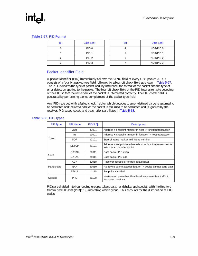
Intel® 82801DBM ICH4-M Datasheet 199
Functional Description
Packet Identifier Field
A packet identifier (PID) immediately follows the SYNC field of every USB packet. A PID consists of a four bit packet type field followed by a four-bit check field as shown in Table 5-67. The PID indicates the type of packet and, by inference, the format of the packet and the type of error detection applied to the packet. The four-bit check field of the PID insures reliable decoding of the PID so that the remainder of the packet is interpreted correctly. The PID check field is generated by performing a ones complement of the packet type field.
Any PID received with a failed check field or which decodes to a non-defined value is assumed to be corrupted and the remainder of the packet is assumed to be corrupted and is ignored by the receiver. PID types, codes, and descriptions are listed in Table 5-68.
PIDs are divided into four coding groups: token, data, handshake, and special, with the first two transmitted PID bits (PID[1:0]) indicating which group. This accounts for the distribution of PID codes.
Table 5-67. PID Format
Bit Data Sent Bit Data Sent
0 PID 0 4 NOT(PID 0)
1 PID 1 5 NOT(PID 1)
2 PID 2 6 NOT(PID 2)
3 PID 3 7 NOT(PID 3)
Table 5-68. PID Types
PID Type PID Name PID[3:0] Description
Token
OUT b0001 Address + endpoint number in host -> function transaction
IN b1001 Address + endpoint number in function -> host transaction
SOF b0101 Start of frame marker and frame number
SETUP b1101 Address + endpoint number in host -> function transaction for setup to a control endpoint
DataDATA0 b0011 Data packet PID even
DATA1 b1011 Data packet PID odd
Handshake
ACK b0010 Receiver accepts error free data packet
NAK b1010 Rx device cannot accept data or Tx device cannot send data
STALL b1110 Endpoint is stalled
Special PRE b1100 Host-issued preamble. Enables downstream bus traffic to low speed devices.

200 Intel® 82801DBM ICH4-M Datasheet
Functional Description
5.16.4.4 Address Fields
Function endpoints are addressed using two fields: the function address field and the endpoint field.
Address Field
The function address (ADDR) field specifies the function, via its address, that is either the source or destination of a data packet, depending on the value of the token PID. As shown in Table 5-69, a total of 128 addresses are specified as ADDR[6:0]. The ADDR field is specified for IN, SETUP, and OUT tokens.
Endpoint Field
An additional four-bit endpoint (ENDP) field, shown in Table 5-70, permits more flexible addressing of functions in which more than one sub-channel is required. Endpoint numbers are function specific. The endpoint field is defined for IN, SETUP, and OUT token PIDs only.
5.16.4.5 Frame Number Field
The frame number field is an 11-bit field that is incremented by the host on a per frame basis. The frame number field rolls over upon reaching its maximum value of x7FFh, and is sent only for SOF tokens at the start of each frame.
5.16.4.6 Data Field
The data field may range from 0 to 1023 bytes and must be an integral numbers of bytes. Data bits within each byte are shifted out LSB first.
Table 5-69. Address Field
Bit Data Sent Bit Data Sent
0 ADDR 0 4 ADDR 4
1 ADDR 1 5 ADDR 5
2 ADDR 2 6 ADDR 6
3 ADDR 3
Table 5-70. Endpoint Field
Bit Data Sent
0 ENDP 0
1 ENDP 1
2 ENDP 2
3 ENDP 3

Intel® 82801DBM ICH4-M Datasheet 201
Functional Description
5.16.4.7 Cyclic Redundancy Check (CRC)
CRC is used to protect the all non-PID fields in token and data packets. In this context, these fields are considered to be protected fields. The PID is not included in the CRC check of a packet containing CRC. All CRCs are generated over their respective fields in the transmitter before bit stuffing is performed. Similarly, CRCs are decoded in the receiver after stuffed bits have been removed. Token and data packet CRCs provide 100% coverage for all single and double bit errors. A failed CRC is considered to indicate that one or more of the protected fields is corrupted and causes the receiver to ignore those fields, and, in most cases, the entire packet.
5.16.5 Packet Formats
5.16.5.1 Token Packets
Table 5-71 shows the field formats for a token packet. A token consists of a PID, specifying either IN, OUT, or SETUP packet type, and ADDR and ENDP fields. For OUT and SETUP transactions, the address and endpoint fields uniquely identify the endpoint that will receive the subsequent data packet. For IN transactions, these fields uniquely identify which endpoint should transmit a data packet. Only the ICH4 can issue token packets. IN PIDs define a data transaction from a function to the ICH4. OUT and SETUP PIDs define data transactions from the ICH4 to a function.
Token packets have a five-bit CRC that covers the address and endpoint fields as shown above. The CRC does not cover the PID, which has its own check field. Token and SOF packets are delimited by an EOP after three bytes of packet field data. If a packet decodes as an otherwise valid token or SOF but does not terminate with an EOP after three bytes, it must be considered invalid and ignored by the receiver.
5.16.5.2 Start of Frame Packets
Table 5-72 shows a start of frame (SOF) packet. SOF packets are issued by the host at a nominal rate of once every 1.00 ms 0.05. SOF packets consist of a PID indicating packet type followed by an 11-bit frame number field.
The SOF token comprises the token-only transaction that distributes a start of frame marker and accompanying frame number at precisely timed intervals corresponding to the start of each frame. All full speed functions, including hubs, must receive and decode the SOF packet. The SOF token does not cause any receiving function to generate a return packet; therefore, SOF delivery to any given function cannot be guaranteed. The SOF packet delivers two pieces of timing information. A function is informed that a start of frame has occurred when it detects the SOF PID. Frame timing sensitive functions, which do not need to keep track of frame number, need only decode the SOF PID; they can ignore the frame number and its CRC. If a function needs to track frame number, it must comprehend both the PID and the time stamp.
Table 5-71. Token Format
Packet Width
PID 8 bits
ADDR 7 bits
ENDP 4 bits
CRC5 5 bits

202 Intel® 82801DBM ICH4-M Datasheet
Functional Description
5.16.5.3 Data Packets
A data packet consists of a PID, a data field, and a CRC as shown in Table 5-73. There are two types of data packets, identified by differing PIDs: DATA0 and DATA1. Two data packet PIDs are defined to support data toggle synchronization.
Data must always be sent in integral numbers of bytes. The data CRC is computed over only the data field in the packet and does not include the PID, which has its own check field.
5.16.5.4 Handshake Packets
Handshake packets consist of only a PID. Handshake packets are used to report the status of a data transaction and can return values indicating successful reception of data, flow control, and stall conditions. Only transaction types that support flow control can return handshakes. Handshakes are always returned in the handshake phase of a transaction and may be returned, instead of data, in the data phase. Handshake packets are delimited by an EOP after one byte of packet field. If a packet is decoded as an otherwise valid handshake but does not terminate with an EOP after one byte, it must be considered invalid and ignored by the receiver.
There are three types of handshake packets:
� ACK indicates that the data packet was received without bit stuff or CRC errors over the data field and that the data PID was received correctly. An ACK handshake is applicable only in transactions in which data has been transmitted and where a handshake is expected. ACK can be returned by the host for IN transactions and by a function for OUT transactions.
� NAK indicates that a function was unable to accept data from the host (OUT) or that a function has no data to transmit to the host (IN). NAK can only be returned by functions in the data phase of IN transactions or the handshake phase of OUT transactions. The host can never issue a NAK. NAK is used for flow control purposes to indicate that a function is temporarily unable to transmit or receive data, but will eventually be able to do so without need of host intervention. NAK is also used by interrupt endpoints to indicate that no interrupt is pending.
� STALL is returned by a function in response to an IN token or after the data phase of an OUT. STALL indicates that a function is unable to transmit or receive data, and that the condition requires host intervention to remove the stall. Once a function�s endpoint is stalled, the function must continue returning STALL until the condition causing the stall has been cleared through host intervention. The host is not permitted to return a STALL under any condition.
Table 5-72. SOF Packet
Packet Width
PID 8 bits
Frame Number 11 bits
CRC5 5 bits
Table 5-73. Data Packet Format
Packet Width
PID 8 bits
DATA 0�1023 bytes
CRC16 16 bits

Intel® 82801DBM ICH4-M Datasheet 203
Functional Description
5.16.5.5 Handshake Responses
IN Transaction
A function may respond to an IN transaction with a STALL or NAK. If the token received was corrupted, the function will issue no response. If the function can transmit data, it will issue the data packet. The ICH4, as the USB host, can return only one type of handshake on an IN transaction, an ACK. If it receives a corrupted data, or cannot accept data due to a condition such as an internal buffer overrun, it discards the data and issues no response.
OUT Transaction
A function may respond to an OUT transaction with a STALL, ACK, or NAK. If the transaction contained corrupted data, it will issue no response.
SETUP Transaction
Setup defines a special type of host to function data transaction which permits the host to initialize an endpoint�s synchronization bits to those of the host. Upon receiving a Setup transaction, a function must accept the data. Setup transactions cannot be STALLed or NAKed and the receiving function must accept the Setup transfer�s data. If a non-control endpoint receives a SETUP PID, it must ignore the transaction and return no response.
5.16.6 USB InterruptsThere are two general groups of USB interrupt sources, those resulting from execution of transactions in the schedule, and those resulting from an ICH4 operation error. All transaction-based sources can be masked by software through the ICH4�s Interrupt Enable register. Additionally, individual transfer descriptors can be marked to generate an interrupt on completion.
When the ICH4 drives an interrupt for USB, it internally drives the PIRQ[A]# pin for USB function #0, PIRQ[D]# pin for USB function #1, and the PIRQ[C]# pin for USB function #2, until all sources of the interrupt are cleared. To accommodate some operating systems, the Interrupt Pin register must contain a different value for each function of this new multi-function device.
5.16.6.1 Transaction Based Interrupts
These interrupts are not signaled until after the status for the last complete transaction in the frame has been written back to host memory. This guarantees that software can safely process through (Frame List Current Index -1) when it is servicing an interrupt.
CRC Error / Time-Out
A CRC/Time-Out error occurs when a packet transmitted from the ICH4 to a USB device or a packet transmitted from a USB device to the ICH4 generates a CRC error. The ICH4 is informed of this event by a time-out from the USB device or by the ICH4�s CRC checker generating an error on reception of the packet. Additionally, a USB bus time-out occurs when USB devices do not respond to a transaction phase within 19-bit times of an EOP. Either of these conditions will cause the C_ERR field of the TD to decrement.

204 Intel® 82801DBM ICH4-M Datasheet
Functional Description
When the C_ERR field decrements to zero, the following occurs:
� The Active bit in the TD is cleared
� The Stalled bit in the TD is set
� The CRC/Time-out bit in the TD is set.
� At the end of the frame, the USB Error Interrupt bit is set in the HC status register.
If the CRC/Time out interrupt is enabled in the Interrupt Enable register, a hardware interrupt will be signaled to the system.
Interrupt on Completion
Transfer Descriptors contain a bit that can be set to cause an interrupt on their completion. The completion of the transaction associated with that block causes the USB Interrupt bit in the HC Status Register to be set at the end of the frame in which the transfer completed. When a TD is encountered with the IOC bit set to 1, the IOC bit in the HC Status register is set to 1 at the end of the frame if the active bit in the TD is set to 0 (even if it was set to zero when initially read).
If the IOC Enable bit of Interrupt Enable register (bit 2 of I/O offset 04h) is set, a hardware interrupt is signaled to the system. The USB Interrupt bit in the HC status register is set either when the TD completes successfully or because of errors. If the completion is because of errors, the USB Error bit in the HC status register is also set.
Short Packet Detect
A transfer set is a collection of data which requires more than 1 USB transaction to completely move the data across the USB. An example might be a large print file which requires numerous TDs in multiple frames to completely transfer the data. Reception of a data packet that is less than the endpoint�s Max Packet size during Control, Bulk or Interrupt transfers signals the completion of the transfer set, even if there are active TDs remaining for this transfer set. Setting the SPD bit in a TD indicates to the HC to set the USB Interrupt bit in the HC status register at the end of the frame in which this event occurs. This feature streamlines the processing of input on these transfer types. If the Short Packet Interrupt Enable bit in the Interrupt Enable register is set, a hardware interrupt is signaled to the system at the end of the frame where the event occurred.
Serial Bus Babble
When a device transmits on the USB for a time greater than its assigned Max Length, it is said to be babbling. Since isochrony can be destroyed by a babbling device, this error results in the Active bit in the TD being cleared to 0 and the Stalled and Babble bits being set to one. The C_ERR field is not decremented for a babble. The USB Error Interrupt bit in the HC Status register is set to 1 at the end of the frame. A hardware interrupt is signaled to the system.
If an EOF babble was caused by the ICH4 (due to incorrect schedule for instance), the ICH4 will force a bit stuff error followed by an EOP and the start of the next frame.
Stalled
This event indicates that a device/endpoint returned a STALL handshake during a transaction or that the transaction ended in an error condition. The TDs Stalled bit is set and the Active bit is cleared. Reception of a STALL does not decrement the error counter. A hardware interrupt is signaled to the system.

Intel® 82801DBM ICH4-M Datasheet 205
Functional Description
Data Buffer Error
This event indicates that an overrun of incoming data or a under-run of outgoing data has occurred for this transaction. This would generally be caused by the ICH4 not being able to access required data buffers in memory within necessary latency requirements. Either of these conditions will cause the C_ERR field of the TD to be decremented.
When C_ERR decrements to zero, the Active bit in the TD is cleared, the Stalled bit is set, the USB Error Interrupt bit in the HC Status register is set to 1 at the end of the frame and a hardware interrupt is signaled to the system.
Bit Stuff Error
A bit stuff error results from the detection of a sequence of more that 6 ones in a row within the incoming data stream. This will cause the C_ERR field of the TD to be decremented. When the C_ERR field decrements to zero, the Active bit in the TD is cleared to 0, the Stalled bit is set to 1, the USB Error Interrupt bit in the HC Status register is set to 1 at the end of the frame and a hardware interrupt is signaled to the system.
5.16.6.2 Non-Transaction Based Interrupts
If an ICH4 process error or system error occur, the ICH4 halts and immediately issues a hardware interrupt to the system.
Resume Received
This event indicates that the ICH4 received a RESUME signal from a device on the USB bus during a global suspend. If this interrupt is enabled in the Interrupt Enable register, a hardware interrupt will be signaled to the system allowing the USB to be brought out of the suspend state and returned to normal operation.
ICH4 Process Error
The HC monitors certain critical fields during operation to ensure that it does not process corrupted data structures. These include checking for a valid PID and verifying that the MaxLength field is less than 1280. If it detects a condition that would indicate that it is processing corrupted data structures, it immediately halts processing, sets the HC Process Error bit in the HC Status register and signals a hardware interrupt to the system.
This interrupt cannot be disabled through the Interrupt Enable register.
Host System Error
The ICH4 sets this bit to 1 when a PCI Parity error, PCI Master Abort, or PCI Target Abort occur. When this error occurs, the ICH4 clears the Run/Stop bit in the Command register to prevent further execution of the scheduled TDs. This interrupt cannot be disabled through the Interrupt Enable register.

206 Intel® 82801DBM ICH4-M Datasheet
Functional Description
5.16.7 USB Power ManagementThe Host Controller can be put into a suspended state and its power can be removed. This requires that certain bits of information are retained in the resume power plane of the ICH4 so that a device on a port may wake the system. Such a device may be a fax-modem, which will wake up the machine to receive a fax or take a voice message. The settings of the following bits in I/O space will be maintained when the ICH4 enters the S3, S4 or S5 states:
When the ICH4 detects a resume event on any of its ports, it will set the corresponding USB_STS bit in ACPI space. If USB is enabled as a wake/break event, the system will wake up and an SCI will be generated.
5.16.8 USB Legacy Keyboard OperationWhen a USB keyboard is plugged into the system, and a standard keyboard is not, the system may not boot, and DOS legacy software will not run, because the keyboard will not be identified. The ICH4 implements a series of trapping operations which will snoop accesses that go to the keyboard controller, and put the expected data from the USB keyboard into the keyboard controller.
Note: The scheme described below assumes that the keyboard controller (8042 or equivalent) is on the LPC bus.
This legacy operation is performed through SMM space. Figure 5-19 shows the Enable and Status path. The latched SMI source (60R, 60W, 64R, 64W) is available in the Status Register. Because the enable is after the latch, it is possible to check for other events that didn't necessarily cause an SMI. It is the software's responsibility to logically AND the value with the appropriate enable bits.
Note also that the SMI is generated before the PCI cycle completes (e.g., before TRDY# goes active) to ensure that the processor does not complete the cycle before the SMI is observed. This method is used on MPIIX and has been validated.
The logic will also need to block the accesses to the 8042. If there is an external 8042, then this is simply accomplished by not activating the 8042 CS. This is simply done by logically ANDing the 4 enables (60R, 60W, 64R, 64W) with the 4 types of accesses to determine if 8042CS should go active. An additional term is required for the �Pass-through� case.
The state table for the diagram is shown in Table 5-75.
Table 5-74. Bits Maintained in Low Power States
Register Offset Bit Description
Command 00h 3 Enter Global Suspend Mode (EGSM)
Status 02h 2 Resume Detect
Port Status and Control 10h & 12h
2 Port Enabled/Disabled
6 Resume Detect
8 Low Speed Device Attached
12 Suspend

Intel® 82801DBM ICH4-M Datasheet 207
Functional Description
Figure 5-19. USB Legacy Keyboard Enable and Status Paths
KBC Accesses
PCI Config
Read, Write
60 READ
Clear SMI_60_R
EN_SMI_ON_60RComb.
DecoderAND
Same for 60W, 64R, 64W
SMIOR
To Individual"Caused By"
"Bits"
To PIRQD#
To "Caused By" Bit
AND
AND
EN_PIRQD#
USB_IRQ
Clear USB_IRQ
EN_SMI_ON_IRQ
SD
R
SD
R

208 Intel® 82801DBM ICH4-M Datasheet
Functional Description
Table 5-75. USB Legacy Keyboard State Transitions
Current State Action Data Value Next State Comment
IDLE 64h / Write D1h GateState1Standard D1 command. Cycle passed through to 8042. SMI# doesn't go active. PSTATE (offset C0, bit 6) goes to 1.
IDLE 64h / Write Not D1h IDLE Bit 3 in configuration register determines if cycle passed through to 8042 and if SMI# generated.
IDLE 64h / Read N/A IDLE Bit 2 in configuration register determines if cycle passed through to 8042 and if SMI# generated.
IDLE 60h / Write Don't Care IDLE Bit 1 in configuration register determines if cycle passed through to 8042 and if SMI# generated.
IDLE 60h / Read N/A IDLE Bit 0 in configuration register determines if cycle passed through to 8042 and if SMI# generated.
GateState1 60h / Write XXh GateState2Cycle passed through to 8042, even if trap enabled in Bit 1 in configuration register. No SMI# generated. PSTATE remains 1. If data value is not DFh or DDh, then the 8042 may chose to ignore it.
GateState1 64h / Write D1h GateState1
Cycle passed through to 8042, even if trap enabled via Bit 3 in configuration register. No SMI# generated. PSTATE remains 1. Stay in GateState1 because this is part of the double-trigger sequence.
GateState1 64h / Write Not D1h ILDEBit 3 in configuration space determines if cycle passed through to 8042 and if SMI# generated. PSTATE goes to 0. If Bit 7 in Configuration register is set, then SMI# should be generated.
GateState1 60h / Read N/A IDLE
This is an invalid sequence. Bit 0 in configuration register determines if cycle passed through to 8042 and if SMI# generated. PSTATE goes to 0. If Bit 7 in configuration register is set, then SMI# should be generated.
GateState1 64h / Read N/A GateState1Just stay in same state. Generate an SMI# if enabled in Bit 2 of configuration register. PSTATE remains 1.
GateState2 64 / Write FFh IDLEStandard end of sequence. Cycle passed through to 8042. PSTATE goes to 0. Bit 7 in configuration space determines if SMI# should be generated.
GateState2 64h / Write Not FFh IDLE
Improper end of sequence. Bit 3 in the configuration register determines if cycle passed through to 8042 and if SMI# generated. PSTATE goes to 0. If Bit 7 in the configuration register is set, then SMI# should be generated.
GateState2 64h / Read N/A GateState2Just stay in same state. Generate an SMI# if enabled in Bit 2 of configuration register. PSTATE remains 1.
GateState2 60h / Write XXh IDLE
Improper end of sequence. Bit 1 in the configuration register determines if cycle passed through to 8042 and if SMI# generated. PSTATE goes to 0. If Bit 7 in configuration register is set, then SMI# should be generated.
GateState2 60h / Read N/A IDLE
Improper end of sequence. Bit 0 in the configuration register determines if cycle passed through to 8042 and if SMI# generated. PSTATE goes to 0. If Bit 7 in configuration register is set, then SMI# should be generated.

Intel® 82801DBM ICH4-M Datasheet 209
Functional Description
5.17 USB EHCI Controller (D29:F7)The ICH4 contains an Enhanced Host Controller Interface (EHCI) compliant host controller which supports up to 6 high-speed USB 2.0 Specification compliant root ports. High-speed USB 2.0 allows data transfers up to 480 Mbps using the same pins as the 6 Full-speed/Low-speed USB UHCI ports. The ICH4 contains port-routing logic that determines whether a USB port is controlled by one of the UHCI controllers or by the EHCI controller. A USB 2.0 based Debug Port is also implemented in the ICH4.
A summary of the key architectural differences between the USB UHCI host controllers and the USB EHCI host controller are shown in Table 5-76.
5.17.1 EHC InitializationThe following descriptions step through the expected ICH4 Enhanced Host Controller (EHC) initialization sequence in chronological order, beginning with a complete power cycle in which the suspend well and core well have been off.
5.17.1.1 Power On
The suspend well is a �deeper� power plane than the core well, which means that the suspend well is always functional when the core well is functional but the core well may not be functional when the suspend well is. Therefore, the suspend well reset pin (RSMRST#) deasserts before the core well reset pin (PWROK) rises.
1. The suspend well reset deasserts, leaving all registers and logic in the suspend well in the default state. However, it is not possible to read any registers until after the core well reset deasserts. Note that normally the suspend well reset will only occur when the battery is removed. In other words, suspend well resets are not easily achieved by software or the end-user. This step will typically not occur immediately before the remaining steps.
2. The core well reset deasserts, leaving all registers and logic in the core well in the default state. The EHC configuration space is accessible at this point. Note that the core well reset can (and typically does) occur without the suspend well reset asserting. This means that all of the Configure Flag and Port Status and Control bits (and any other suspend-well logic) may be in any valid state at this time.
5.17.1.2 BIOS Initialization
BIOS performs a number of platform customization steps after the core well has powered up. Contact your intel field sales representative for the latest BIOS information.
Table 5-76. UHCI vs. EHCI
Topic USB UHCI USB EHCI
Accessible by I/O space Memory Space
Memory Data Structure Single linked list Separated in to Periodic and Asynchronous lists
Differential Signaling Voltage 3.3 V 400 mV
Ports per Controller 2 6

210 Intel® 82801DBM ICH4-M Datasheet
Functional Description
5.17.1.3 Driver Initialization
See Chapter 4 of the Enhanced Host Controller Interface Specification for Universal Serial Bus.
5.17.1.4 EHC Resets
In addition to the standard ICH4 hardware resets, portions of the EHC are reset by the HCRESET bit and the transition from the D3hot device power management state to the D0 state. The effects of each of these resets are listed in the following table.
If the detailed register descriptions give exceptions to these rules, those exceptions override these rules. This summary is provided to help explain the reasons for the reset policies.
5.17.2 Data Structures in Main MemorySee Chapter 3 and Appendix B of the Enhanced Host Controller Interface Specification for Universal Serial Bus for details.
5.17.3 USB 2.0 Enhanced Host Controller DMAThe ICH4 USB 2.0 EHC implements three sources of USB packets. They are, in order of priority on USB during each microframe,
1. the USB 2.0 Debug Port (see Section USB 2.0 EHCI Based Debug Port),
2. the Periodic DMA engine, and
3. the Asynchronous DMA engine.
The ICH4 always performs any currently-pending debug port transaction at the beginning of a microframe, followed by any pending periodic traffic for the current microframe. If there is time left in the microframe, then the EHC performs any pending asynchronous traffic until the end of the microframe (EOF1). Note that the debug port traffic is only presented on one port (Port #0), while the other ports are idle during this time.
The following subsections describe the policies of the periodic and asynchronous DMA engines.
Reset Does Reset Does not Reset Comments
HCRESET bit set
Memory space registers except Structural Parameters (which is written by BIOS)
Configuration registers
The HCRESET must only affect registers that the EHCI driver controls. PCI Configuration space and BIOS-programmed parameters can not be reset.
Software writes the Device Power State from D3hot (11b) to D0 (00b)
Core well registers (except BIOS-programmed registers)
Suspend well registers; BIOS-programmed core well registers
The D3-to-D0 transition must not cause wake information (suspend well) to be lost. It also must not clear BIOS-programmed registers because BIOS may not be invoked following the D3-to-D0 transition.

Intel® 82801DBM ICH4-M Datasheet 211
Functional Description
5.17.3.1 Periodic List Execution
The Periodic DMA engine contains buffering for two control structures (two transactions). By implementing two entries, the EHC is able to pipeline the memory accesses for the next transaction while executing the current transaction on the USB ports. Note that a multiple-packet, High-Bandwidth transaction occupies one of these buffer entries, which means that up to six 1-kB data packets may be associated with the two buffered control structures.
5.17.3.1.1 Read Policies for Periodic DMA
The Periodic DMA engine performs reads for the following structures.
The EHC Periodic DMA Engine (PDE) does not generate accesses to main memory unless all three of the following conditions are met.
� The HCHalted bit is 0 (memory space, offset 24h, bit 12). Software clears this bit indirectly by setting the RUN/STOP bit to 1.
� The Periodic Schedule Status bit is 1 (memory space, offset 24h, bit 14). Software sets this bit indirectly by setting the Periodic Schedule Enable Bit to 1.
� The Bus Master Enable bit is 1 (configuration space, offset 04h, bit 2).
Note: Prefetching is limited to the current and next microframes only.
Note: Once the PDE checks the length of a periodic packet against the remaining time in the microframe (late-start check) and decides that there is not enough time to run it on the wire, then the EHC switches over to run asynchronous traffic.
Memory Structure Size (DWords) Comments
Periodic Frame List entry 1 The EHC reads the entry for each microframe. The frame list is not internally cached across microframes.
iTD 23 Only the 64-bit addressing format is supported.
siTD 9 Only the 64-bit addressing format is supported.
qTD 13 Only the 64-bit addressing format is supported.
Queue Head 17 Only the 64-bit addressing format is supported.
Out Data Up to 257The ICH4 breaks large read requests down into smaller aligned read requests based on the setting of the Read Request Max Length field.
Frame Span Transversal Node 2

212 Intel® 82801DBM ICH4-M Datasheet
Functional Description
5.17.3.1.2 Write Policies for Periodic DMAThe Periodic DMA engine performs writes for the following reasons.
NOTES:1. The Periodic DMA Engine (PDE) will only generate writes after a transaction is executed on USB.2. Status writes are always performed after In Data writes for the same transaction.
5.17.3.2 Asynchronous List Execution
The Asynchronous DMA engine contains buffering for two control structures (two transactions). By implementing two entries, the EHC is able to pipeline the memory accesses for the next transaction while executing the current transaction on the USB ports.
5.17.3.2.1 Read Policies for Asynchronous DMAThe Asynchronous DMA engine performs reads for the following structures.
The EHC Asynchronous DMA Engine (ADE) does not generate accesses to main memory unless all four of the following conditions are met. (Note that the ADE may be active when the periodic schedule is actively executed, unlike the description in the EHCI specification; since the EHC contains independent DMA engines, the ADE may perform memory accesses interleaved with the PDE accesses.)
� The HCHalted bit is 0 (memory space, offset 24h, bit 12). Software clears this bit indirectly by setting the RUN/STOP bit to 1.
� The Asynchronous Schedule Status bit is 1 (memory space, offset 24h, bit 14). Software sets this bit indirectly by setting the Asynchronous Schedule Enable Bit to 1.
� The Bus Master Enable bit is 1 (configuration space, offset 04h, bit 2).� The ADE is not sleeping due to the detection of an empty schedule. There is not one single bit
that indicates this state. However, the sleeping state is entered when the Queue Head with the H bit set is encountered when the Reclamation bit in the USB EHCI Status register is 0.
Memory Structure Size (DWords) Comments
iTD Status Write 1 Only the DWord that corresponds to the just-executed microframe�s status is written. All bytes of the DWord are written.
siTD Status Write 3 DWords 0C:17h are written. IOC and Buffer Pointer fields are re-written with the original value.
Interrupt Queue Head Overlay 14 Only the 64-bit addressing format is supported. DWords 0C:43h are
written.
Interrupt Queue Head Status Write 54 DWords 14:27h are written.
Interrupt qTD Status Write 3 DWords 04:0Fh are written. PID Code, IOC, Buffer Pointers, and Alt.
Next qTD Pointers are re-written with the original value.
In Data Up to 257 The ICH4 breaks data writes down into 16 DWord aligned chunks.
Memory Structure Size (DW) Comments
qTD 13 Only the 64-bit addressing format is supported.
Queue Head 17 Only the 64-bit addressing format is supported.
Out Data Up to 129The ICH4 breaks large read requests down in to smaller aligned read requests based on the setting of the Read Request Max Length field.

Intel® 82801DBM ICH4-M Datasheet 213
Functional Description
Note: The ADE does not fetch data when a QH is encountered in the Ping state. An Ack handshake in response to the Ping results in the ADE writing the QH to the Out state, which results in the fetching and delivery of the Out Data on the next iteration through the asynchronous list.
Note: Once the ADE checks the length of an asynchronous packet against the remaining time in the microframe (late-start check) and decides that there is not enough time to run it on the wire, then the EHC stops all activity on the USB ports for the remainder of that microframe.
Note: Once the ADE detects an �empty� asynchronous schedule as described in Chapter 4 of the Enhanced Host Controller Interface (EHCI) Specification for Universal Serial Bus, it implements a waking mechanism like the one in the example. The amount of time that the ADE �sleeps� is 10 µs ± 30 ns.
5.17.3.2.2 Write Policies for Asynchronous DMA
The Asynchronous DMA engine performs writes for the following reasons.
NOTES:1. The Asynchronous DMA Engine (ADE) will only generate writes after a transaction is executed on USB.2. Status writes are always performed after In Data writes for the same transaction.
5.17.4 Data Encoding and Bit StuffingSee Chapter 8 of the Universal Serial Bus (USB) Specification, Revision 2.0.
5.17.5 Packet FormatsSee Chapter 8 of the Universal Serial Bus (USB) Specification, Revision 2.0.
Memory Structure Size (DWords) Comments
Asynchronous Queue Head Overlay 14 Only the 64-bit addressing format is supported. DWords 0C:43h are
written.
Asynchronous Queue Head Status Write
34 DWords 14:1Fh are written.
Asynchronous qTD Status Write 3 DWords 04:0Fh are written. PID Code, IOC, Buffer Pointer (Page 0),
and Alt. Next qTD Pointers are re-written with the original value.
In Data Up to 1297 The ICH4 breaks data writes down into 16 DWord aligned chunks.

214 Intel® 82801DBM ICH4-M Datasheet
Functional Description
5.17.6 USB EHCI Interrupts and Error ConditionsSection 4 of the EHCI specification goes into detail on the EHC interrupts and the error conditions that cause them. All error conditions that the EHC detects can be reported through the EHCI Interrupt status bits. Only ICH4-specific interrupt and error-reporting behavior is documented in this section. The EHCI Interrupts Section must be read first, followed by this section of the datasheet to fully comprehend the EHC interrupt and error-reporting functionality.
� Based on the EHC�s buffer sizes and buffer management policies, the Data Buffer Error can never occur on the ICH4.
� Master Abort and Target Abort responses from hub interface on EHC-initiated read packets will be treated as Fatal Host Errors. The EHC halts when these conditions are encountered.
� The ICH4 may assert the interrupts which are based on the interrupt threshold as soon as the status for the last complete transaction in the interrupt interval has been posted in the internal write buffers. The requirement in the EHCI Specification (that the status is written to memory) is met internally, even though the write may not be seen on the hub interface before the interrupt is asserted.
� Since the ICH4 supports the 1024-element Frame List size, the Frame List Rollover interrupt occurs every 1024 milliseconds.
� The ICH4 delivers interrupts using PIRQ#[H].
� The ICH4 does not modify the CERR count on an Interrupt IN when the �Do Complete-Split� execution criteria are not met.
� For complete-split transactions in the Periodic list, the �Missed Microframe� bit does not get set on a control-structure-fetch that fails the late-start test. If subsequent accesses to that control structure do not fail the late-start test, then the �Missed Microframe� bit will get set and written back.
5.17.6.1 Aborts on USB EHCI-Initiated Memory Reads
If a read initiated by the EHC is aborted, the EHC treats it as a fatal host error. The following actions are taken when this occurs:
� The Host System Error status bit is set
� The DMA engines are halted after completing up to one more transaction on the USB interface
� If enabled (by the Host System Error Enable), an interrupt is generated
� If the status is Master Abort, the Received Master Abort bit in configuration space is set
� If the status is Target Abort, the Received Target Abort bit in configuration space is set
� If enabled (by the SERR Enable bit in the function�s configuration space), the Signaled System Error bit in configuration bit is set.
5.17.7 USB EHCI Power Management
5.17.7.1 Pause Feature
This feature allows platforms (especially mobile systems) to dynamically enter low-power states during brief periods when the system is idle (i.e., between keystrokes). This is useful for enabling power management features like C3, C4, and Intel SpeedStep technology in the ICH4. The policies
Intel® 82801DBM ICH4-M Datasheet 215
Functional Description
for entering these states typically are based on the recent history of system bus activity to incrementally enter deeper power management states. Normally, when the EHC is enabled, it regularly accesses main memory while traversing the DMA schedules looking for work to do; this activity is viewed by the power management software as a non-idle system, thus preventing the power managed states to be entered. Suspending all of the enabled ports can prevent the memory accesses from occurring, but there is an inherent latency overhead with entering and exiting the suspended state on the USB ports that makes this unacceptable for the purpose of dynamic power management. As a result, the EHCI software drivers are allowed to pause the EHC�s DMA engines when it knows that the traffic patterns of the attached devices can afford the delay. The pause only prevents the EHC from generating memory accesses; the SOF packets continue to be generated on the USB ports (unlike the suspended state).
5.17.7.2 Suspend Feature
The Enhanced Host Controller Interface (EHCI) for Universal Serial Bus Specification describes the details of Port Suspend and Resume in detail in Section 4.3.
5.17.7.3 ACPI Device States
The USB EHCI function only supports the D0 and D3 PCI Power Management states. Notes regarding the ICH4 implementation of the Device States:
� The EHC hardware does not inherently consume any more power when it is in the D0 state than it does in the D3 state. However, software is required to suspend or disable all ports prior to entering the D3 state such that the maximum power consumption is reduced.
� In the D0 state, all implemented EHC features are enabled.
� In the D3 state, accesses to the EHC memory-mapped I/O range will master abort. Note that, since the Debug Port uses the same memory range, the Debug Port is only operational when the EHC is in the D0 state.
� In the D3 state, the EHC interrupt must never assert for any reason. The internal PME# signal is used to signal wake events, etc.
� When the Device Power State field is written to D0 from D3, an internal reset is generated. See section EHC Resets for general rules on the effects of this reset.
� Attempts to write any other value into the Device Power State field other than 00b (D0 state) and 11b (D3 state) will complete normally without changing the current value in this field.

216 Intel® 82801DBM ICH4-M Datasheet
Functional Description
5.17.7.4 ACPI System States
The EHC behavior as it relates to other power management states in the system is summarized in the following list:
� The System is always in the S0 state when the EHC is in the D0 state. However, when the EHC is in the D3 state, the system may be in any power management state (including S0).
� When in D0, the Pause feature (See Section 5.17.7.1) enables dynamic processor low-power states to be entered.
� The PLL in the EHC is disabled when entering the S1-M state (48 MHz clock stops), or the S3/S4/S5 states (core power turns off).
� All core well logic is reset in the S3/S4/S5 states (core power turns off).
5.17.7.5 Mobile Considerations
The ICH4 USB EHCI implementation does not behave differently in the mobile configurations versus the desktop configurations. However, some features may be especially useful for the mobile configurations.
� Mobile systems are not likely to use all 6 of the USB ports that are provided on the ICH4. With this in mind, the ICH4 provides mechanisms for changing the structural parameters of the EHC and hiding unused USB UHCI controllers. See ICH4 BIOS Specification on how BIOS should configure the ICH4.
� Mobile systems may want to minimize the conditions that will wake the system. The ICH4 implements the �Wake Enable� bits in the Port Status and Control registers, as specified in the EHCI specification, for this purpose.
� Mobile systems may want to cut suspend well power to some or all USB ports when in a low-power state. The ICH4 implements the optional Port Wake Capability Register in the EHC Configuration Space for this platform-specific information to be communicated to software.
5.17.8 Interaction with Classic Host ControllersThe Enhanced Host Controller shares the 6 USB ports with 3 UHCI Host Controllers in the ICH4. The USB UHCI Controller at D29:F0 shares ports 0 and 1; the USB UHCI Controller at D29:F1 shares ports 2 and 3; and the USB UHCI Controller at D29:F2 shares ports 4 and 5 with the EHCI Controller. There is very little interaction between the USB EHCI and the USB UHCI controllers other than the muxing control which is provided as part of the EHCI Controller.
Figure 5-20 depicts the USB Port Connections at a conceptual level. The dashed rectangle indicates all of the logic that is part of the Enhanced Host Controller cluster.

Intel® 82801DBM ICH4-M Datasheet 217
Functional Description
5.17.8.1 Port-Routing Logic
Integrated into the EHC functionality is port-routing logic, which performs the muxing between the USB UHCI and USB EHCI host controllers. The ICH4 conceptually implements this logic as described in Section 4.2 of the Enhanced Host Controller Interface (EHCI) for Universal Serial Bus Specification. If a device is connected that is not capable of USB 2.0�s high-speed signaling protocol or if the EHCI software drivers are not present as indicated by the Configured Flag, then the USB UHCI Controller owns the port. Owning the port means that the differential output is driven by the owner and the input stream is only visible to the owner. The host controller that is not the owner of the port internally sees a disconnected port.
Note that the port-routing logic is the only block of logic within the ICH4 that observes the physical (real) connect/disconnect information. The port status logic inside each of the host controllers observes the electrical connect/disconnect information that is generated by the port-routing logic.
Only the differential signal pairs are muxed/demuxed between the USB UHCI and USB EHCI host controllers. The other USB functional signals are handled as follows:
� The Overcurrent inputs (OC#[5:0]) are directly routed to both controllers. An overcurrent event is recorded in both controller�s status registers.
The Port-Routing logic is implemented in the Suspend power well so that re-enumeration and re-mapping of the USB ports is not required following entering and exiting a system sleep state in which the core power is turned off.
The ICH4 also allows the USB Debug Port traffic to be routed in and out of Port #0. When in this mode, the Enhanced Host Controller is the owner of Port #0.
Figure 5-20. Intel® ICH4 USB Port Connections
Port 0
Port 1
Port 2
Port 3
Port 4
Port 5
UHCI #3 (D29:F2)
UHCI #2 (D29:F1)
UHCI #1 (D29:F0)
EHCI (D29:F7) Debug Port

218 Intel® 82801DBM ICH4-M Datasheet
Functional Description
5.17.8.2 Device Connects
Section 4.2 of the Enhanced Host Controller Interface (EHCI) for Universal Serial Bus Specification describes the details of handling Device Connects. There are four general scenarios that are summarized below.
1. Configure Flag = 0 and a USB Full-speed/Low-speed -only Device is connected� In this case, the USB UHCI Controller is the owner of the port both before and after the
connect occurs. The EHC (except for the port-routing logic) never sees the connect occur. The UHCI driver handles the connection and initialization process.
2. Configure Flag = 0 and an USB High-speed-capable Device is connected� In this case, the USB UHCI Controller is the owner of the port both before and after the
connect occurs. The EHC (except for the port-routing logic) never sees the connect occur. The UHCI driver handles the connection and initialization process. Since the USB UHCI Controller does not perform the high-speed chirp handshake, the device operates in compatible mode.
3. Configure Flag = 1 and a USB Full-speed/Low-speed-only Device is connected� In this case, the USB EHCI Controller is the owner of the port before the connect occurs.
The EHCI driver handles the connection and performs the port reset. After the reset process completes, the EHC hardware has cleared (not set) the Port Enable bit in the EHC�s PORTSC register. The EHCI driver then writes a 1 to the Port Owner bit in the same register, causing the USB UHCI Controller to see a connect event and the EHC to see an �electrical� disconnect event. The UHCI driver and hardware handle the connection and initialization process from that point on. The EHCI driver and hardware handle the perceived disconnect.
4. Configure Flag = 1 and an USB High-speed-capable Device is connected� In this case, the USB EHCI Controller is the owner of the port before, and remains the
owner after, the connect occurs. The EHCI driver handles the connection and performs the port reset. After the reset process completes, the EHC hardware has set the Port Enable bit in the EHC�s PORTSC register. The port is functional at this point. The USB UHCI Controller continues to see an unconnected port.
5.17.8.3 Device Disconnects
Section 4.2 of the Enhanced Host Controller Interface (EHCI) for Universal Serial Bus Specification describes the details of handling Device Connects. There are three general scenarios that are summarized below.
1. Configure Flag = 0 and the device is disconnected� In this case, the USB UHCI Controller is the owner of the port both before and after the
disconnect occurs. The EHC (except for the port-routing logic) never sees a device attached. The UHCI driver handles disconnection process.
2. Configure Flag = 1 and a USB Full-speed/Low-speed-capable Device is disconnected� In this case, the USB UHCI Controller is the owner of the port before the disconnect
occurs. The disconnect is reported by the USB UHCI Controller and serviced by the associated UHCI driver. The port-routing logic in the EHC cluster forces the Port Owner bit to 0, indicating that the EHC owns the unconnected port.
3. Configure Flag = 1 and a USB High-speed-capable Device is disconnected� In this case, the USB EHCI Controller is the owner of the port before, and remains the
owner after, the disconnect occurs. The EHCI hardware and driver handle the disconnection process. The USB UHCI Controller never sees a device attached.

Intel® 82801DBM ICH4-M Datasheet 219
Functional Description
5.17.8.4 Effect of Resets on Port-Routing Logic
As mentioned above, the Port Routing logic is implemented in the Suspend power well so that re-enumeration and re-mapping of the USB ports is not required following entering and exiting a system sleep state in which the core power is turned off.
5.17.9 USB 2.0 Legacy Keyboard OperationThe ICH4 must support the possibility of a keyboard downstream from either a USB UHCI or a USB EHCI port. The description of the legacy keyboard support is unchanged from USB UHCI (See Section 5.16.8).
The EHC provides the basic ability to generate SMIs on an interrupt event, along with more sophisticated control of the generation of SMIs.
Reset Event Effect on Configure Flag Effect on Port Owner Bits
Suspend Well Reset cleared (0) set (1)
Core Well Reset no effect no effect
D3-to-D0 Reset no effect no effect
HCRESET cleared (0) set (1)

220 Intel® 82801DBM ICH4-M Datasheet
Functional Description
5.17.10 USB 2.0 EHCI Based Debug PortThe ICH4 supports the elimination of the legacy COM ports by providing the ability for new debugger software to interact with devices on a USB EHCI port. High-level restrictions and features are:
� Must be operational before USB EHCI drivers are loaded.� Must work even when the port is disabled.� Must work even though non-configured port is default-routed to the classic controller. Note
that the Debug Port can not be used to debug an issue that requires a classic USB device on Port #0 using the UHCI drivers.
� Must allow normal system USB EHCI traffic in a system that may only have one USB port.� Debug Port device (DPD) must be High-Speed capable and connect to a High-Speed port on
ICH4 systems.� Debug Port FIFO must always make forward progress (a bad status on USB is simply
presented back to software)� The Debug Port FIFO is only given one USB access per microframe
The Debug port facilitates OS and device driver debug. It allows the software to communicate with an external console using a USB EHCI connection. Because the interface to this link does not go through the normal USB EHCI stack, it allows communication with the external console during cases where the OS is not loaded, the USB EHCI software is broken, or where the USB EHCI software is being debugged. Specific features of this implementation of a debug port are:
� Only works with an external USB 2.0 debug device (console)
� Implemented for a specific port on the host controller
� Operational anytime the port is not suspended AND the host controller is in D0 power state.
� Capability is interrupted when port is driving USB RESET
5.17.10.1 Theory of Operation
There are two operational modes for the USB debug port:� Mode 1 is when the USB port is in a disabled state from the viewpoint of a standard host
controller driver. In Mode 1, the Debug Port controller is required to generate a �keepalive� packets less than 2 ms apart to keep the attached debug device from suspending. The keepalive packet should be a standalone 32-bit SYNC field.
� Mode 2 is when the host controller is running (i.e., Host controller�s Run/Stop# bit is 1). In Mode 2, the normal transmission of SOF packets will keep the debug device from suspending.
Behavioral Rules
1. In both modes 1 and 2, the Debug Port controller must check for software requested debug transactions at least every 125 microseconds.
2. If the debug port is enabled by the debug driver, and the standard host controller driver resets the USB port, USB debug transactions are held off for the duration of the reset and until after the first SOF is sent.
3. If the standard host controller driver suspends the USB port, then USB debug transactions are held off for the duration of the suspend/resume sequence and until after the first SOF is sent.
4. The ENABLED_CNT bit in the debug register space is independent of the similar port control bit in the associated Port Status and Control register.

Intel® 82801DBM ICH4-M Datasheet 221
Functional Description
Table 5-77 shows the debug port behavior related to the state of bits in the debug registers as well as bits in the associated Port Status and Control register.
5.17.10.1.1OUT Transactions
An Out transaction sends data to the debug device. It can occur only when the following are true:
� The debug port is enabled� The debug software sets the GO_CNT bit� The WRITE_READ#_CNT bit is set
The sequence of the transaction is:
1. Software sets the appropriate values in the following bits: � USB_ADDRESS_CNF� USB_ENDPOINT_CNF� DATA_BUFFER[63:0]� TOKEN_PID_CNT[7:0]� SEND_PID_CNT[15:8]� DATA_LEN_CNT� WRITE_READ#_CNT (note: this will always be 1 for OUT transactions)� GO_CNT (note: this will always be 1 to initiate the transaction)
Table 5-77. Debug Port Behavior
OWNER_CNT ENABLED_CT Port Enable
Run / Stop Suspend Debug Port Behavior
0 X X X X Debug port is not being used. Normal operation.
1 0 X X X Debug port is not being used. Normal operation.
1 1 0 0 X Debug port in Mode 1. SYNC keepalives sent plus debug traffic
1 1 0 1 X
Debug port in Mode 2. SOF (and only SOF) is sent as keepalive. Debug traffic is also sent. Note that no other normal traffic is sent out this port, because the port is not enabled.
1 1 1 0 0Illegal. Host controller driver should never put controller into this state (enabled, not running and not suspended).
1 1 1 0 1 Port is suspended. No debug traffic sent.
1 1 1 1 0Debug port in Mode 2. Debug traffic is interspersed with normal traffic.
1 1 1 1 1 Port is suspended. No debug traffic sent.

222 Intel® 82801DBM ICH4-M Datasheet
Functional Description
2. The debug port controller sends a token packet consisting of� SYNC� TOKEN_PID_CNT field� USB_ADDRESS_CNT field� USB_ENDPOINT_CNT field� 5-bit CRC field
3. After sending the token packet, the debug port controller sends a data packet consisting of� SYNC� SEND_PID_CNT field� The number of data bytes indicated in DATA_LEN_CNT from the DATA_BUFFER� 16-bit CRC
Note: A DATA_LEN_CNT value of zero is valid in which case no data bytes would be included in the packet.
4. After sending the data packet, the controller waits for a handshake response from the debug device.
� If a handshake is received, the debug port controller:� a. Places the received PID in the RECEIVED_PID_STS field� b. Resets the ERROR_GOOD#_STS bit� c. Sets the DONE_STS bit
� If no handshake PID is received, the debug port controller:� a. Sets the EXCEPTION_STS field to 001b� b. Sets the ERROR_GOOD#_STS bit� c. Sets the DONE_STS bit
5.17.10.1.2 IN Transactions
An IN transaction receives data from the debug device. It can occur only when the following are true:
� The debug port is enabled
� The debug software sets the GO_CNT bit
� The WRITE_READ#_CNT bit is reset
The sequence of the transaction is:
1. Software sets the appropriate values in the following bits:
� USB_ADDRESS_CNF
� USB_ENDPOINT_CNF
� TOKEN_PID_CNT[7:0]
� DATA_LEN_CNT
� WRITE_READ#_CNT (note: this will always be 0 for IN transactions)
� GO_CNT (note: this will always be 1 to initiate the transaction)

Intel® 82801DBM ICH4-M Datasheet 223
Functional Description
2. The debug port controller sends a token packet consisting of:
� SYNC
� TOKEN_PID_CNT field
� USB_ADDRESS_CNT field
� USB_ENDPOINT_CNT field
� 5-bit CRC field.
3. After sending the token packet, the debug port controller waits for a response from the debug device.If a response is received:
� The received PID is placed into the RECEIVED_PID_STS field
� Any subsequent bytes are placed into the DATA_BUFFER
� The DATA_LEN_CNT field is updated to show the number of bytes that were received after the PID.
4. If valid packet was received from the device that was one byte in length (indicating it was a handshake packet), then the debug port controller:
� Resets the ERROR_GOOD#_STS bit
� Sets the DONE_STS bit
5. If valid packet was received from the device that was more than one byte in length (indicating it was a data packet), then the debug port controller:
� Transmits an ACK handshake packet
� Resets the ERROR_GOOD#_STS bit
� Sets the DONE_STS bit
6. If no valid packet is received, then the debug port controller:
� Sets the EXCEPTION_STS field to 001b
� Sets the ERROR_GOOD#_STS bit
� Sets the DONE_STS bit.
5.17.10.1.3 Debug Software
Enabling the Debug Port
There are two mutually exclusive conditions that debug software must address as part of its startup processing:
� The EHCI has been initialized by system software
� The EHCI has not been initialized by system software
Debug software can determine the current �initialized� state of the EHCI by examining the Configure Flag in the EHCI USB 2.0 Command Register. If this flag is set, then system software has initialized the EHCI. Otherwise, the EHCI should not be considered initialized. Debug software will initialize the debug port registers depending on the state the EHCI. However, before this can be accomplished, debug software must determine which root USB port is designated as the debug port.

224 Intel® 82801DBM ICH4-M Datasheet
Functional Description
Determining the Debug Port
Debug software can easily determine which USB root port has been designated as the debug port by examining bits 20:23 of the EHCI Host Controller Structural Parameters register. This 4-bit field represents the numeric value assigned to the debug port (i.e., 0000=port 0).
Debug Software Startup with Non-Initialized EHCI
Debug software can attempt to use the debug port if after setting the OWNER_CNT bit, the Current Connect Status bit in the appropriate (See Determining the Debug Port) PORTSC register is set. If the Current Connect Status bit is not set, then debug software may choose to terminate or it may choose to wait until a device is connected.
If a device is connected to the port, then debug software must reset/enable the port. Debug software does this by setting and then clearing the Port Reset bit the PORTSC register. To guarantee a successful reset, debug software should wait at least 50 ms before clearing the Port Reset bit. Due to possible delays, this bit may not change to 0 immediately; reset is complete when this bit reads as 0. Software must not continue until this bit reads 0.
If a high-speed device is attached, the EHCI will automatically set the Port Enabled/Disabled bit in the PORTSC register and the debug software can proceed. Debug software should set the ENABLED_CNT bit in the Debug Port Control/Status register, and then reset (clear) the Port Enabled/Disabled bit in the PORTSC register (so that the system host controller driver does not see an enabled port when it is first loaded).
Debug Software Startup with Initialized EHCI
Debug software can attempt to use the debug port if the Current Connect Status bit in the appropriate (See Determining the Debug Port) PORTSC register is set. If the Current Connect Status bit is not set, then debug software may choose to terminate or it may choose to wait until a device is connected.
If a device is connected, then debug software must set the OWNER_CNT bit and then the ENABLED_CNT bit in the Debug Port Control/Status register.
Determining Debug Peripheral Presence
After enabling the debug port functionality, debug software can determine if a debug peripheral is attached by attempting to send data to the debug peripheral. If all attempts result in an error (Exception bits in the Debug Port Control/Status register indicates a Transaction Error), then the attached device is not a debug peripheral. If the debug port peripheral is not present, then debug software may choose to terminate or it may choose to wait until a debug peripheral is connected.

Intel® 82801DBM ICH4-M Datasheet 225
Functional Description
5.18 SMBus Controller Functional Description (D31:F3)The ICH4 provides an SMBus 2.0 compliant Host Controller as well as an SMBus Slave Interface. The Host Controller provides a mechanism for the processor to initiate communications with SMBus peripherals (slaves). The ICH4 is also capable of operating in a mode in which it can communicate with I2C compatible devices.
The ICH4 can perform SMBus messages with either packet error checking (PEC) enabled or disabled. The actual PEC calculation and checking is performed in hardware by the ICH4.
The Slave Interface allows an external master to read from or write to the ICH4. Write cycles can be used to cause certain events or pass messages, and the read cycles can be used to determine the state of various status bits. The ICH4�s internal Host Controller cannot access the ICH4�s internal Slave Interface.
The ICH4 SMBus logic exists in Device 31:Function 3 configuration space, and consists of a transmit data path and host controller. The transmit data path provides the data flow logic needed to implement the seven different SMBus command protocols and is controlled by the host controller. The ICH4 SMBus controller logic is clocked by RTC clock.
The SMBus Address Resolution Protocol (ARP) is supported by using the existing host controller commands through software, except for the new Host Notify command (which is actually a received message).
The programming model of the host controller is combined into two portions: a PCI configuration portion and a system I/O mapped portion. All static configuration (e.g., the I/O base address) is done via the PCI configuration space. Real-time programming of the Host interface is done in system I/O space.
5.18.1 Host ControllerThe SMBus Host Controller is used to send commands to other SMBus slave devices. Software sets up the host controller with an address, command, and, for writes, data and optional PEC; and then tells the controller to start. When the controller has finished transmitting data on writes, or receiving data on reads, it will generate an SMI# or interrupt, if enabled.
The host controller supports 8 command protocols of the SMBus interface (see System Management Bus Specification): Quick Command, Send Byte, Receive Byte, Write Byte/Word, Read Byte/Word, Process Call, Block Read/Write, and Host Notify.
The SMBus Host Controller requires that the various data and command fields be setup for the type of command to be sent. When software sets the START bit, the SMBus Host Controller performs the requested transaction and interrupts the processor (or generate an SMI#) when the transaction is completed. Once a START command has been issued, the values of the �active registers� (Host Control, Host Command, Transmit Slave Address, Data 0, Data 1) should not be changed or read until the interrupt status bit (INTR) has been set (indicating the completion of the command). Any register values needed for computation purposes should be saved prior to issuing of a new command, as the SMBus Host Controller will update all registers while completing the new command.

226 Intel® 82801DBM ICH4-M Datasheet
Functional Description
Using the SMB Host Controller to send commands to the ICH4's SMB slave port is supported. The ICH4 supports slave functionality, including the Host Notify protocol, on the SMLink pins. Therefore, to be fully compliant with the SMBus 2.0 specification (which requires the Host Notify protocol), the SMLink and SMBus signals should be tied together externally.
5.18.1.1 Command Protocols
In all of the following commands, the Host Status Register (offset 00h) is used to determine the progress of the command. While the command is in operation, the HOST_BUSY bit is set. If the command completes successfully, the INTR bit will be set in the Host Status Register. If the device does not respond with an acknowledge, and the transaction times out, the DEV_ERR bit is set. If software sets the KILL bit in the Host Control Register while the command is running, the transaction will stop and the FAILED bit will be set.
Quick Command
When programmed for a Quick Command, the Transmit Slave Address Register is sent. The PEC byte is never appended to the Quick Protocol. Software should force the PEC_EN bit to 0 when performing the Quick Command. Software must force the I2C_EN bit to 0 when running this command.The format of the protocol is shown in Table 5-78.
Send Byte / Receive Byte
For the Send Byte command, the Transmit Slave Address and Device Command Registers are sentFor the Receive Byte command, the Transmit Slave Address Register is sent. The data received is stored in the DATA0 register. Software must force the I2C_EN bit to 0 when running this command.
The Receive Byte is similar to a Send Byte, the only difference is the direction of data transfer. The format of the protocol is shown in Table 5-79. and Table 5-80
Table 5-78. Quick Protocol
Bit Description
1 Start Condition2�8 Slave Address - 7 bits
9 Read / Write Direction10 Acknowledge from slave11 Stop
Table 5-79. Send / Receive Byte Protocol without PEC
Send Byte Protocol Receive Byte Protocol
Bit Description Bit Description
1 Start 1 Start2�8 Slave Address - 7 bits 2�8 Slave Address - 7 bits
9 Write 9 Read10 Acknowledge from slave 10 Acknowledge from slave
11�18 Command code - 8 bits 11�18 Data byte from slave19 Acknowledge from slave 19 NOT Acknowledge20 Stop 20 Stop

Intel® 82801DBM ICH4-M Datasheet 227
Functional Description
Write Byte/Word
The first byte of a Write Byte/Word access is the command code. The next 1 or 2 bytes are the data to be written. When programmed for a Write Byte/Word command, the Transmit Slave Address, Device Command, and Data0 Registers are sent. In addition, the Data1 Register is sent on a Write Word command. Software must force the I2C_EN bit to 0 when running this command. The format of the protocol is shown in Table 5-81 and Table 5-82.
Table 5-80. Send/Receive Byte Protocol with PEC
Send Byte Protocol Receive Byte Protocol
Bit Description Bit Description
1 Start 1 Start
2�8 Slave Address - 7 bits 2�8 Slave Address - 7 bits
9 Write 9 Read
10 Acknowledge from slave 10 Acknowledge from slave
11�18 Command code - 8 bits 11�18 Data byte from slave
19 Acknowledge from slave 19 Acknowledge
20�27 PEC 20�27 PEC from slave
28 Acknowledge from slave 28 Not Acknowledge
29 Stop 29 Stop
Table 5-81. Write Byte/Word Protocol without PEC
Write Byte Protocol Write Word Protocol
Bit Description Bit Description
1 Start 1 Start
2�8 Slave Address - 7 bits 2�8 Slave Address - 7 bits
9 Write 9 Write
10 Acknowledge from slave 10 Acknowledge from slave
11�18 Command code - 8 bits 11�18 Command code - 8 bits
19 Acknowledge from slave 19 Acknowledge from slave
20�27 Data Byte - 8 bits 20�27 Data Byte Low - 8 bits
28 Acknowledge from Slave 28 Acknowledge from Slave
29 Stop 29�36 Data Byte High - 8 bits
37 Acknowledge from slave
38 Stop

228 Intel® 82801DBM ICH4-M Datasheet
Functional Description
Read Byte/Word
Reading data is slightly more complicated than writing data. First the ICH4 must write a command to the slave device. Then it must follow that command with a repeated start condition to denote a read from that device's address. The slave then returns 1 or 2 bytes of data. Software must force the I2C_EN bit to 0 when running this command.
When programmed for the read byte/word command, the Transmit Slave Address and Device Command Registers are sent. Data is received into the DATA0 on the read byte, and the DAT0 and DATA1 registers on the read word. The format of the protocol is shown in Table 5-83 and Table 5-84.
Table 5-82. Write Byte/Word Protocol with PEC
Write Byte Protocol Write Word Protocol
Bit Description Bit Description
1 Start 1 Start
2�8 Slave Address - 7 bits 2�8 Slave Address - 7 bits
9 Write 9 Write
10 Acknowledge from slave 10 Acknowledge from slave
11�18 Command code - 8 bits 11�18 Command code - 8 bits
19 Acknowledge from slave 19 Acknowledge from slave
20�27 Data Byte - 8 bits 20�27 Data Byte Low - 8 bits
28 Acknowledge from Slave 28 Acknowledge from Slave
29�36 PEC 29�36 Data Byte High - 8 bits
37 Acknowledge from Slave 37 Acknowledge from slave
38 Stop 38�45 PEC
46 Acknowledge from slave
47 Stop

Intel® 82801DBM ICH4-M Datasheet 229
Functional Description
Table 5-83. Read Byte/Word Protocol without PEC
Read Byte Protocol Read Word Protocol
Bit Description Bit Description
1 Start 1 Start
2�8 Slave Address - 7 bits 2�8 Slave Address - 7 bits
9 Write 9 Write
10 Acknowledge from slave 10 Acknowledge from slave
11�18 Command code - 8 bits 11�18 Command code - 8 bits
19 Acknowledge from slave 19 Acknowledge from slave
20 Repeated Start 20 Repeated Start
21�27 Slave Address - 7 bits 21�27 Slave Address - 7 bits
28 Read 28 Read
29 Acknowledge from slave 29 Acknowledge from slave
30�37 Data from slave - 8 bits 30�37 Data Byte Low from slave - 8 bits
38 NOT acknowledge 38 Acknowledge
39 Stop 39�46 Data Byte High from slave - 8 bits
47 NOT acknowledge
48 Stop
Table 5-84. Read Byte/Word Protocol with PEC
Read Byte Protocol Read Word Protocol
Bit Description Bit Description
1 Start 1 Start
2�8 Slave Address - 7 bits 2�8 Slave Address - 7 bits
9 Write 9 Write
10 Acknowledge from slave 10 Acknowledge from slave
11�18 Command code - 8 bits 11�18 Command code - 8 bits
19 Acknowledge from slave 19 Acknowledge from slave
20 Repeated Start 20 Repeated Start
21�27 Slave Address - 7 bits 21�27 Slave Address - 7 bits
28 Read 28 Read
29 Acknowledge from slave 29 Acknowledge from slave
30�37 Data from slave - 8 bits 30�37 Data Byte Low from slave - 8 bits
38 Acknowledge 38 Acknowledge
39�46 PEC from slave 39�46 Data Byte High from slave - 8 bits
47 NOT Acknowledge 47 Acknowledge
48 Stop 48�55 PEC from slave
56 NOT acknowledge
57 Stop

230 Intel® 82801DBM ICH4-M Datasheet
Functional Description
Process Call
The process call is so named because a command sends data and waits for the slave to return a value dependent on that data. The protocol is simply a Write Word followed by a Read Word, but without a second command or stop condition.
When programmed for the Process Call command, the ICH4 transmits the Transmit Slave Address, Host Command, DATA0 and DATA1 registers. Data received from the device is stored in the DATA0 and DATA1 registers. The Process Call command with I2C_EN set and the PEC_EN bit set produces undefined results. Software must force either I2C_EN or PEC_EN to 0 when running this command. The format of the protocol is shown in Table 5-85 and Table 5-86.
Note: For process call command, the value written into bit 0 of the Transmit Slave Address Register (SMB I/O register, offset 04h) needs to be 0.
Table 5-85. Process Call Protocol without PEC
Bit Description
1 Start
2�8 Slave Address - 7 bits
9 Write
10 Acknowledge from Slave
11�18(Skip This step if I2C_EN bit set) Command code - 8 bits
19(Skip This step if I2C_EN bit set) Acknowledge from slave
20�27 Data byte Low - 8 bits
28 Acknowledge from slave
29�36 Data Byte High - 8 bits
37 Acknowledge from slave
38 Repeated Start
39�45 Slave Address - 7 bits
46 Read
47 Acknowledge from slave
48�55 Data Byte Low from slave - 8 bits
56 Acknowledge
57�64 Data Byte High from slave - 8 bits
65 NOT acknowledge
66 Stop

Intel® 82801DBM ICH4-M Datasheet 231
Functional Description
Block Read/Write
The ICH4 contains a 32-byte buffer for read and write data which can be enabled by setting bit 1 of the Auxiliary Control register at offset 0Dh in I/O space, as opposed to a single byte of buffering. This 32-byte buffer is filled with write data before transmission, and filled with read data on reception. In the ICH4, the interrupt is generated only after a transmission or reception of 32 bytes, or when the entire byte count has been transmitted/received.
This requires the ICH4 to check the byte count field. Currently, the byte count field is transmitted but ignored by the hardware as software will end the transfer after all bytes it cares about have been sent or received.
For a Block Write software must either force the I2C_EN bit or both the PEC_EN and AAC bits to 0 when running this command.
SMBus mode: The block write begins with a slave address and a write condition. After the command code the ICH4 issues a byte count describing how many more bytes will follow in the message. If a slave had 20 bytes to send, the first byte would be the number 20 (14h), followed by 20 bytes of data. The byte count may not be 0. A Block Read or Write is allowed to transfer a maximum of 32 data bytes.
Table 5-86. Process Call Protocol with PEC
Bit Description
1 Start
2�8 Slave Address - 7 bits
9 Write
10 Acknowledge from Slave
11�18 Command code - 8 bits
19 Acknowledge from slave
20�27 Data byte Low - 8 bits
28 Acknowledge from slave
29�36 Data Byte High - 8 bits
37 Acknowledge from slave
38 Repeated Start
39�45 Slave Address - 7 bits
46 Read
47 Acknowledge from slave
48�55 Data Byte Low from slave - 8 bits
56 Acknowledge
57�64 Data Byte High from slave - 8 bits
65 Acknowledge
66�73 PEC from slave
74 NOT acknowledge
75 Stop

232 Intel® 82801DBM ICH4-M Datasheet
Functional Description
When programmed for a block write command, the Transmit Slave Address, Device Command, and Data0 (count) registers are sent. Data is then sent from the Block Data Byte register; the total data sent being the value stored in the Data0 Register. On block read commands, the first byte received is stored in the Data0 register, and the remaining bytes are stored in the Block Data Byte register.
The format of the Block Read/Write protocol is shown in Table 5-87 and Table 5-88.
Note: For Block Write, if the I2C_EN bit is set, the format of the command changes slightly. The ICH4 will still send the number of bytes (on writes) or receive the number of bytes (on reads) indicated in the DATA0 register. However, it will not send the contents of the DATA0 register as part of the message.
l
Table 5-87. Block Read/Write Protocol without PEC
Block Write Protocol Block Read Protocol
Bit Description Bit Description
1 Start 1 Start
2�8 Slave Address - 7 bits 2�8 Slave Address - 7 bits
9 Write 9 Write
10 Acknowledge from slave 10 Acknowledge from slave
11�18 Command code - 8 bits 11�18 Command code - 8 bits
19 Acknowledge from slave 19 Acknowledge from slave
20�27 Byte Count - 8 bits 20 Repeated Start
28 Acknowledge from Slave 21�27 Slave Address - 7 bits
29�36 Data Byte 1 - 8 bits 28 Read
37 Acknowledge from Slave 29 Acknowledge from slave
38�45 Data Byte 2 - 8 bits 30�37 Byte Count from slave - 8 bits
46 Acknowledge from slave 38 Acknowledge
...Data Bytes / Slave Acknowledges...
39�46 Data Byte 1 from slave - 8 bits
... Data Byte N - 8 bits 47 Acknowledge
... Acknowledge from Slave 48�55 Data Byte 2 from slave - 8 bits
... Stop 56 Acknowledge
... Data Bytes from slave/Acknowledge
... Data Byte N from slave - 8 bits
... NOT Acknowledge
... Stop

Intel® 82801DBM ICH4-M Datasheet 233
Functional Description
I2C Read
This command allows the ICH4 to perform block reads to certain I2C devices (e.g., serial E2PROMs) in 10-bit addressing mode only. The SMBus Block Read sends both the 7-bit address, as well as the Command field. This command field could be used as the extended 10-bit address for accessing I2C devices that use 10-bit addressing.
However, this does not allow access to devices using the I2C �Combined Format� that has data bytes after the address. Typically these data bytes correspond to an offset (address) within the serial memory chips.
Note: This command is supported independent of the setting of the I2C_EN bit. The I2C Read command with the PEC_EN bit set produces undefined results. Software must force both the PEC_EN and AAC bit to 0 when running this command.
Table 5-88. Block Read/Write Protocol with PEC
Block Write Protocol Block Read Protocol
Bit Description Bit Description
1 Start 1 Start
2�8 Slave Address - 7 bits 2�8 Slave Address - 7 bits
9 Write 9 Write
10 Acknowledge from slave 10 Acknowledge from slave
11�18 Command code - 8 bits 11�18 Command code - 8 bits
19 Acknowledge from slave 19 Acknowledge from slave
20�27Byte Count - 8 bits(Skip this step if I2C_En bit set)
20 Repeated Start
28Acknowledge from Slave(Skip this step if I2C_EN bit set)
21�27 Slave Address - 7 bits
29�36 Data Byte 1 - 8 bits 28 Read
37 Acknowledge from Slave 29 Acknowledge from slave
38�45 Data Byte 2 - 8 bits 30�37 Byte Count from slave - 8 bits
46 Acknowledge from slave 38 Acknowledge
...Data Bytes / Slave Acknowledges...
39�46 Data Byte 1 from slave - 8 bits
... Data Byte N - 8 bits 47 Acknowledge
... Acknowledge from Slave 48�55 Data Byte 2 from slave - 8 bits
... PEC - 8 bits 56 Acknowledge
... Acknowledge from Slave ... Data Bytes from slave/Acknowledge
... Stop ... Data Byte N from slave - 8 bits
... Acknowledge
... PEC from slave - 8 bits
... NOT Acknowledge
... Stop

234 Intel® 82801DBM ICH4-M Datasheet
Functional Description
For I2C Read command, the value written into bit 0 of the Transmit Slave Address Register (SMB I/O register, offset 04h) needs to be 0. The format that is used for the new command is shown in Table 5-89.
The ICH4 will continue reading data from the peripheral until the NAK is received.
5.18.1.2 I2C Behavior
When the I2C_EN bit is set, the ICH4 SMBus logic will instead be set to communicate with I2C devices. This forces the following changes:
� The Process Call command will skip the Command code (and its associated acknowledge)
� The Block Write command will skip sending the Byte Count (DATA0)
In addition, the ICH4 will support the new I2C Read command. This is independent of the I2C_EN bit.
Note: When operating in I2C mode the ICH4 will not use the 32-byte buffer for block commands.
Table 5-89. I2C Block Read
Bit Description
1 Start
2�8 Slave Address - 7 bits
9 Write
10 Acknowledge from slave
11�18 Command code - 8 bits
19 Acknowledge from slave
20�27 Send DATA0 register
28 Acknowledge from slave
29�36 Send DATA1 register
37 Acknowledge from slave
38 Repeated start
39�45 Slave Address - 7 bits
46 Read
47 Acknowledge from slave
48�55 Data byte from slave
56 Acknowledge
57�64 Data byte 2 from slave - 8 bits
65 Acknowledge
� Data bytes from slave / Acknowledge
� Data byte N from slave - 8 bits
� NOT Acknowledge
� Stop

Intel® 82801DBM ICH4-M Datasheet 235
Functional Description
5.18.1.3 Heartbeat for Use with the External LAN Controller
This method allows the ICH4 to send messages to an external LAN Controller when the processor is otherwise unable to do so. It uses the SMLINK interface between the ICH4 and the external LAN Controller. The actual Heartbeat message is a Block Write. Only 8 bytes are sent.
5.18.2 Bus ArbitrationSeveral masters may attempt to get on the bus at the same time by driving the SMBDATA line low to signal a start condition. The ICH4 must continuously monitor the SMBDATA line. When the ICH4 is attempting to drive the bus to a 1 by letting go of the SMBDATA line, and it samples SMBDATA low, some other master is driving the bus and the ICH4 must stop transferring data.
If the ICH4 sees that it has lost arbitration, the condition is called a collision. The ICH4 will set the BUS_ERR bit in the Host Status Register, and if enabled, generate an interrupt or SMI#. The processor is responsible for restarting the transaction.
When the ICH4 is a SMBus master, it will drive the clock. When the ICH4 is sending address or command as an SMBus master, or data bytes as a master on writes, it will drive data relative to the clock it is also driving. It will not start toggling the clock until the start or stop condition meets proper setup and hold time. The ICH4 will also guarantee minimum time between SMBus transactions as a master.
Note: The ICH4 supports the same arbitration protocol for both the SMBus and the System Management (SMLINK) interfaces.
5.18.3 Bus Timing
5.18.3.1 Clock Stretching
Some devices may not be able to handle their clock toggling at the rate that the ICH4 as an SMBus master would like. They have the capability of stretching the low time of the clock. When the ICH4 attempts to release the clock (allowing the clock to go high), the clock will remain low for an extended period of time.
The ICH4 must monitor the SMBus clock line after it releases the bus to determine whether to enable the counter for the high time of the clock. While the bus is still low, the high time counter must not be enabled. Similarly, the low period of the clock can be stretched by an SMBus master if it is not ready to send or receive data.
5.18.3.2 Bus Time Out (ICH4 as SMBus Master)
If there is an error in the transaction such that an SMBus device does not signal an acknowledge or holds the clock lower than the allowed time-out time, the transaction will time out. The ICH4 discards the cycle and sets the DEV_ERR bit. The time-out minimum is 25 ms. The time-out counter inside the ICH4 will start after the last bit of data is transferred by the ICH4 and it is waiting for a response. The 25 ms is a count of 800 RTC clocks.

236 Intel® 82801DBM ICH4-M Datasheet
Functional Description
5.18.4 Interrupts / SMI#The ICH4 SMBus controller uses PIRQB# as its interrupt pin. However, the system can alternatively be set up to generate SMI# instead of an interrupt, by setting the SMBUS_SMI_EN bit.
Table 5-91 and Table 5-92 specify how the various enable bits in the SMBus function control the generation of the interrupt, Host and Slave SMI, and Wake internal signals. The rows in the tables are additive, which means that if more than one row is true for a particular scenario then the Results for all of the activated rows will occur.
Table 5-90. Enable for SMBALERT#
EventINTREN (Host
Control I/O Register, Offset
02h, Bit 0)
SMB_SMI_EN (Host Configu-ration Register,
D31:F3:Offset 40h, Bit 1)
SMBALERT_DIS (Slave Command I/O Register, Offset 11h,
Bit 2)Result
SMBALERT# asserted low (always reported in Host Status Register, Bit 5)
X X X Wake generated
X 1 0 Slave SMI# generated(SMBUS_SMI_STS)
1 0 0 Interrupt generated
Table 5-91. Enables for SMBus Slave Write and SMBus Host Events
EventINTREN (Host Control
I/O Register, Offset 02h, Bit 0)
SMB_SMI_EN (Host Configuration Register, D31:F3:Offset 40h, Bit1)
Event
Slave Write to Wake/SMI# Command X X
Wake generated when asleep.Slave SMI# generated when awake (SMBUS_SMI_STS).
Slave Write to SMLINK_SLAVE_SMI Command
X X Slave SMI# generated when in the S0 state (SMBUS_SMI_STS)
Any combination of Host Status Register [4:1] asserted
0 X None
1 0 Interrupt generated
1 1 Host SMI# generated
Table 5-92. Enables for the Host Notify Command
HOST_NOTIFY_INTREN (Slave Control I/O Register, Offset 11h, bit 0)
SMB_SMI_EN (Host Configuration Register, D31:F3:Off40h, Bit 1)
HOST_NOTIFY_WKEN (Slave Control I/O Register, Offset 11h, bit 1)
Result
0 X 0 None
X X 1 Wake generated
1 0 X Interrupt generated
1 1 XSlave SMI# generated (SMBUS_SMI_STS)

Intel® 82801DBM ICH4-M Datasheet 237
Functional Description
5.18.5 SMBALERT#SMBALERT# is multiplexed with GPIO[11]. When enable and the signal is asserted, The ICH4 can generate an interrupt, an SMI# or a wake event from S1-M�S5.
Note: Any event on SMBALERT# (regardless whether it is programmed as a GPIO or not), causes the event message to be sent in �heartbeat mode.�
5.18.6 SMBus CRC Generation and CheckingIf the AAC bit is set in the Auxiliary Control register, the ICH4 automatically calculates and drives CRC at the end of the transmitted packet for write cycles and checks the CRC for read cycles. It will not transmit the contents of the PEC register for CRC. The PEC bit must not be set in the Host Control register if this bit is set, or unspecified behavior will result.
If the read cycle results in a CRC error, the DEV_ERR bit and the CRCE bit in the Auxiliary Status register at offset 0Ch will be set.
5.18.7 SMBus Slave InterfaceThe ICH4�s SMBus Slave interface is accessed via the SMLINK[1:0] signals. The SMBus slave logic does not generate or handle receiving the PEC byte and only acts as a Legacy Alerting Protocol (Alert on LAN*) device. The slave interface allows the ICH4 to decode cycles, and allows an external microcontroller to perform specific actions. Key features and capabilities include:
� Supports decode of three types of messages: Byte Write, Byte Read, and Host Notify
� Receive Slave Address register: This is the address that the ICH4 decodes. A default value is provided so that the slave interface can be used without the processor having to program this register.
� Receive Slave Data register in the SMBus I/O space that includes the data written by the external microcontroller
� Registers that the external microcontroller can read to get the state of the ICH4. See Table 5-97
� Status bits to indicate that the SMLink/SMBus slave logic caused an interrupt or SMI# due to the reception of a message that matched the slave address.
� Bit 0 of the Slave Status Register for the Host Notify command
� Bit 16 of the SMI Status Register (Section 9.8.3.13) for all others
If a master leaves the clock and data bits of the SMLink interface at 1 for 50 µs or more in the middle of a cycle, the ICH4 slave logic's behavior is undefined. This is interpreted as an unexpected idle and should be avoided when performing management activities to the slave logic.
Note: When an external micro controller accesses the SMBus Slave Interface over the SMLink a translation in the address is needed to accommodate the least significant bit used for read/write control. For example, if the ICH4 slave address (RCV_SLVA) is left at 44h (default), the external microcontroller would use an address of 88h/89h (write/read).
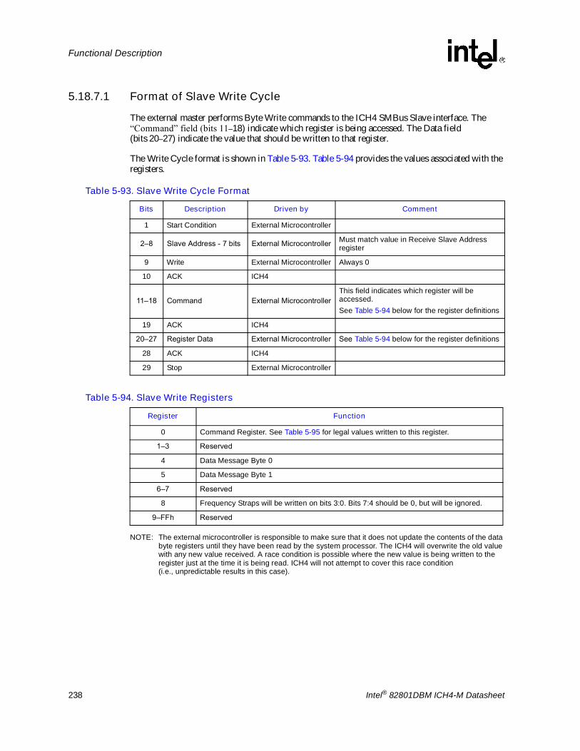
238 Intel® 82801DBM ICH4-M Datasheet
Functional Description
5.18.7.1 Format of Slave Write Cycle
The external master performs Byte Write commands to the ICH4 SMBus Slave interface. The �Command� field (bits 11�18) indicate which register is being accessed. The Data field (bits 20�27) indicate the value that should be written to that register.
The Write Cycle format is shown in Table 5-93. Table 5-94 provides the values associated with the registers.
NOTE: The external microcontroller is responsible to make sure that it does not update the contents of the data byte registers until they have been read by the system processor. The ICH4 will overwrite the old value with any new value received. A race condition is possible where the new value is being written to the register just at the time it is being read. ICH4 will not attempt to cover this race condition (i.e., unpredictable results in this case).
Table 5-93. Slave Write Cycle Format
Bits Description Driven by Comment
1 Start Condition External Microcontroller
2�8 Slave Address - 7 bits External Microcontroller Must match value in Receive Slave Address register
9 Write External Microcontroller Always 0
10 ACK ICH4
11�18 Command External MicrocontrollerThis field indicates which register will be accessed.See Table 5-94 below for the register definitions
19 ACK ICH4
20�27 Register Data External Microcontroller See Table 5-94 below for the register definitions
28 ACK ICH4
29 Stop External Microcontroller
Table 5-94. Slave Write Registers
Register Function
0 Command Register. See Table 5-95 for legal values written to this register.
1�3 Reserved
4 Data Message Byte 0
5 Data Message Byte 1
6�7 Reserved
8 Frequency Straps will be written on bits 3:0. Bits 7:4 should be 0, but will be ignored.
9�FFh Reserved

Intel® 82801DBM ICH4-M Datasheet 239
Functional Description
.
5.18.7.2 Format of Read Command
The external master performs Byte Read commands to the ICH4 SMBus Slave interface. The �Command� field (bits 11�18) indicate which register is being accessed. The Data field (bits 30-37) contain the value that should be read from that register. Table 5-96 shows the Read Cycle format. Table 5-97 shows the register mapping for the data byte.
Table 5-95. Command Types
Command Type Description
0 Reserved
1WAKE/SMI#: Wake system if it is not already awake. If system is already awake, then an SMI# will be generated. NOTE: The SMB_WAK_STS bit will be set by this command, even if the system is already
awake. The SMI handler should then clear this bit.
2 Unconditional Powerdown: This command sets the PWRBTNOR_STS bit, and has the same effect as the Powerbutton Override occurring.
3HARD RESET WITHOUT CYCLING: The will cause a hard reset of the system (does not include cycling of the power supply). This is equivalent to a write to the CF9h register with bits 2:1 set to 1, but bit 3 set to 0.
4 HARD RESET SYSTEM: The will cause a hard reset of the system (including cycling of the power supply). This is equivalent to a write to the CF9h register with bits 3:1 set to 1.
5
Disable the TCO Messages: This command will disable the ICH4 from sending Heartbeat and Event messages (as described in Section 5.13.2). Once this command has been executed, Heartbeat and Event message reporting can only be re-enabled by assertion and deassertion of the RSMRST# signal.
6 WD RELOAD: Reload watchdog timer.
7 Reserved
8
SMLINK_SLV_SMI: When ICH4 detects this command type while in the S0 state, it sets the SMLINK_SLV_SMI_STS bit (see Section 9.9.7). This command should only be used if the system is in an S0 state. If the message is received during S1-M�S5 states, the ICH4 acknowledges it, but the SMLINK_SLV_SMI_STS bit does not get set.NOTE: It is possible that the system transitions out of the S0 state at the same time that the
SMLINK_SLV_SMI command is received. In this case, the SMLINK_SLV_SMI_STS bit may get set but not serviced before the system goes to sleep. Once the system returns to S0, the SMI associated with this bit would then be generated. Software must be able to handle this scenario.
9�FFh Reserved

240 Intel® 82801DBM ICH4-M Datasheet
Functional Description
Table 5-96. Read Cycle Format
Bit Description Driven by: Comment:
1 Start External Microcontroller
2�8 Slave Address � 7 bits External Microcontroller Must match value in Receive Slave Address register
9 Write External Microcontroller Always 0
10 ACK ICH4
11�18 Command code � 8 bits External Microcontroller Indicates which register is being accessed. See Table 5-97.
19 ACK ICH4
20 Repeated Start External Microcontroller
21�27 Slave Address - 7 bits External Microcontroller Must match value in Receive Slave Address register
28 Read External Microcontroller Always 1
29 ACK ICH4
30�37 Data Byte ICH4 Value depends on register being accessed. See Table 5-97.
38 NOT ACK External Microcontroller
39 Stop External Microcontroller
Table 5-97. Data Values for Slave Read Registers (Sheet 1 of 2)
Register Bits Description
0 7:0 Reserved.
1 2:0
System Power State� 000 = S0 � 001 = S1-M� 010 = Reserved � 011 = S3� 100 = S4 � 101 = S5 � 110 = Reserved � 111 = Reserved
1 7:3 Reserved
2 3:0 Frequency Strap Register
2 7:4 Reserved
3 5:0 Watchdog Timer current value
3 7:6 Reserved
4 0 1 = The Intruder Detect (INTRD_DET) bit is set. This indicates that the system cover has probably been opened.
4 1 1 = BTI Temperature Event occurred. This bit will be set if the ICH4�s THRM# input signal is active. Need to take after polarity control.
4 2 Boot-Status. This bit will be 1 when the processor does not fetch the first instruction.

Intel® 82801DBM ICH4-M Datasheet 241
Functional Description
5.18.7.2.1 Behavioral Notes
According to SMBus protocol, Read and Write messages always begin with a Start bit�Address�Write bit sequence. When the ICH4 detects that the address matches the value in the Receive Slave Address register, it will assume that the protocol is always followed and ignore the Write bit (bit 9) and signal an Acknowledge during bit 10 (See Table 5-93 and Table 5-96). In other words, if a Start�Address�Read occurs (which is illegal for SMBus Read or Write protocol) and the address matches the ICH4�s Slave Address, the ICH4 will still grab the cycle.
Also according to SMBus protocol, a Read cycle contains a Repeated Start�Address�Read sequence beginning at bit 20 (See Table 5-96). Once again, if the Address matches the ICH4�s Receive Slave Address, it will assume that the protocol is followed, ignore bit 28, and proceed with the Slave Read cycle.
Note: An external microcontroller must not attempt to access the ICH4�s SMBus Slave logic until at least 1 second after both RTCRST# and RSMRST# are deasserted (high).
5.18.7.3 Format of Host Notify Command
The ICH4 tracks and responds to the standard Host Notify command as specified in the SMBus 2.0 specification. The host address for this command is fixed to 0001000b. If the ICH4 already has data for a previously-received host notify command which has not been serviced yet by the host software (as indicated by the HOST_NOTIFY_STS bit), then it will NACK following the host address byte of the protocol. This allows the host to communicate non-acceptance to the master and retain the host notify address and data values for the previous cycle until host software completely services the interrupt. Table 5-98 shows the Host Notify format.
Note: Host software must always clear the HOST_NOTIFY_STS bit after completing any necessary reads of the address and data registers.
4 3 This bit will be set after the TCO timer times out a second time (Both TIMEOUT and SECOND_TO_STS bits set).
4 6:4 Reserved.
4 7
The bit will reflect the state of the GPI[11]/SMBALERT# signal, and will depend on the GP_INV[11] bit. It does not matter if the pin is configured as GPI[11] or SMBALERT#.
� If the GP_INV[11] bit is 1 then the value of register 4 bit 7 will equal the level of the GPI[11]/SMBALERT# pin (high = 1, low = 0).
� If the GP_INV[11] bit is 0 then the value of register 4 bit 7 will equal the inverse of the level of the GPI[11]/SMBALERT# pin (high = 1, low = 0).
5 0 Unprogrammed FWH bit. This bit will be 1 to indicate that the first BIOS fetch returned FFh, which indicates that the FWH is probably blank.
5 1 Battery Low Status. 1 if the BATLOW# pin is a 0.
5 2 CPU Power Failure Status: 1 if the CPUPWR_FLR bit in the GEN_PMCON_2 register is set.
5 7:3 Reserved
6 7:0 Contents of the Message 1 register. See Section 9.9.9.
7 7:0 Contents of the Message 2 register. See Section 9.9.9.
8 7:0 Contents of the WDSTATUS register. See Section 9.9.10.
9�FFh 7:0 Reserved
Table 5-97. Data Values for Slave Read Registers (Sheet 2 of 2)
Register Bits Description
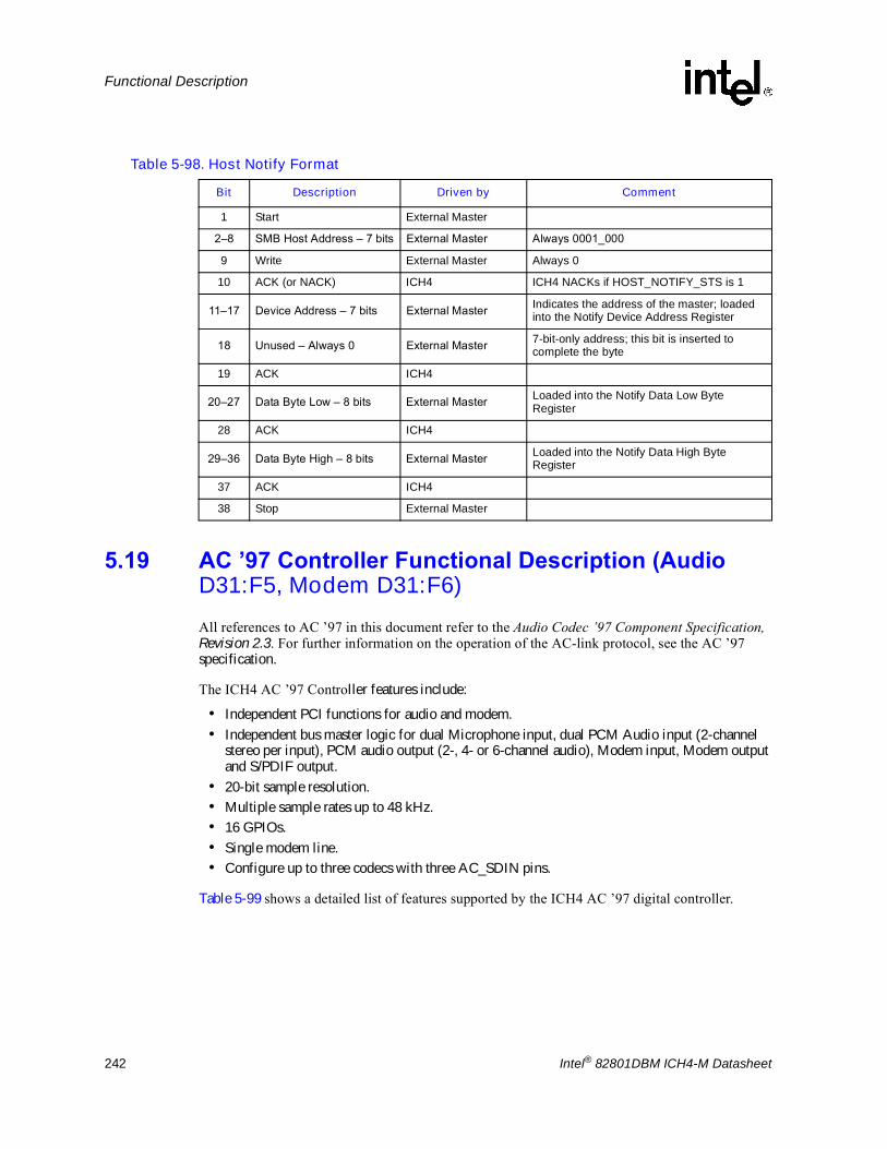
242 Intel® 82801DBM ICH4-M Datasheet
Functional Description
5.19 AC �97 Controller Functional Description (Audio D31:F5, Modem D31:F6)All references to AC �97 in this document refer to the Audio Codec �97 Component Specification, Revision 2.3. For further information on the operation of the AC-link protocol, see the AC �97 specification.
The ICH4 AC �97 Controller features include:
� Independent PCI functions for audio and modem.� Independent bus master logic for dual Microphone input, dual PCM Audio input (2-channel
stereo per input), PCM audio output (2-, 4- or 6-channel audio), Modem input, Modem output and S/PDIF output.
� 20-bit sample resolution.� Multiple sample rates up to 48 kHz.� 16 GPIOs.� Single modem line.� Configure up to three codecs with three AC_SDIN pins.
Table 5-99 shows a detailed list of features supported by the ICH4 AC �97 digital controller.
Table 5-98. Host Notify Format
Bit Description Driven by Comment
1 Start External Master
2�8 SMB Host Address � 7 bits External Master Always 0001_000
9 Write External Master Always 0
10 ACK (or NACK) ICH4 ICH4 NACKs if HOST_NOTIFY_STS is 1
11�17 Device Address � 7 bits External Master Indicates the address of the master; loaded into the Notify Device Address Register
18 Unused � Always 0 External Master 7-bit-only address; this bit is inserted to complete the byte
19 ACK ICH4
20�27 Data Byte Low � 8 bits External Master Loaded into the Notify Data Low Byte Register
28 ACK ICH4
29�36 Data Byte High � 8 bits External Master Loaded into the Notify Data High Byte Register
37 ACK ICH4
38 Stop External Master

Intel® 82801DBM ICH4-M Datasheet 243
Functional Description
.
Table 5-99. Features Supported by Intel® ICH4
Feature Description
System Interface
� Isochronous low latency bus master memory interface� Scatter/gather support for word-aligned buffers in memory.
(all mono or stereo 20-bit and 16-bit data types are supported, no 8-bit data types are supported).
� Data buffer size in system memory from 3 to 65535 samples per input.� Data buffer size in system memory from 0 to 65535 samples per output.� Independent PCI audio and modem functions with configuration and IO spaces.� AC �97 codec registers are shadowed in system memory via driver.� AC �97 codec register accesses are serialized via semaphore bit in PCI IO space
(new accesses are not allowed while a prior access is still in progress).
Power Management � Power management via PCI Power Management
PCI Audio Function
� Read/write access to audio codec registers 00h�3Ah and vendor registers 5Ah�7Eh.� 20-bit stereo PCM output, up to 48 kHz (L,R, Center, Sub-woofer, L-rear and R-rear
channels on slots 3,4,6,7,8,9,10,11).� 16-bit stereo PCM input, up to 48 kHz (L,R channels on slots 3,4).� 16-bit mono mic in w/ or w/o mono mix, up to 48 kHz (L,R channel, slots 3,4) (mono
mix supports mono hardware AEC reference for speakerphone).� 16-bit mono PCM input, up to 48 kHz from dedicated mic ADC (slot 6)
(supports speech recognition or stereo hardware AEC ref for speakerphone).� During cold reset, AC_RST# is held low until after POST and software deassertion of
AC_RST# (supports passive PC_BEEP to speaker connection during POST).
PCI Modem function
� Read/write access to modem codec registers 3Ch�58h and vendor registers 5Ah�7Eh.
� 16-bit mono modem line1 output and input, up to 48 kHz (slot 5). � Low latency GPIO[15:0] via hardwired update between slot 12 and PCI IO register.� Programmable PCI interrupt on modem GPIO input changes via slot 12 GPIO_INT.� SCI event generation on AC_SDIN[2:0] wake-up signals.
AC-link
� Supports AC �97 2.3 AC-link interface. � Variable sample rate output support via AC �97 SLOTREQ protocol
(slots 3,4,5,6,7,8,9,10,11).� Variable sample rate input support via monitoring of slot valid tag bits (slots 3,4,5,6)� 3.3 V digital operation meets AC �97 2.3 DC switching levels. � AC-link IO driver capability meets AC �97 2.3 triple codec specifications.� Codec register status reads must be returned with data in the next AC-link frame, per
the AC �97 2.3 specification.
Multiple Codec
� Triple codec addressing: All AC�97 Audio codec register accesses are addressable to codec ID 00 (primary), codec ID 01 (secondary), or codec ID 10 (tertiary).
� Modem codec addressing: All AC�97 Modem codec register accesses are addressable to codec ID 00 (primary) or codec ID 01 (secondary).
� Triple codec receive capability via AC_SDIN[2:0] pins(AC_SDIN[2:0] frames are internally validated, synch�d, and OR�d depending on the Steer Enable bit status in the SDM register).
� AC_SDIN mapping to DMA engine mapping capability allows for simultaneous input from three different audio codecs.
NOTES:1. Audio Codec IDs are remappable and not limited to 00,01,10.2. Modem Codec IDs are remappable and limited to 00,01.3. When using multiple codecs, the Modem Codec must be ID 01.

244 Intel® 82801DBM ICH4-M Datasheet
Functional Description
Note: Throughout this document, references to D31:F5 indicate that the audio function exists in PCI Device 31, Function 5. References to D31:F6 indicate that the modem function exists in PCI Device 31, Function 6.
Note: Throughout this document, references to tertiary, third, or triple codecs refer to the third codec in the system connected to the AC_SDIN[2] pin. The AC �97 2.3 specification refers to non-primary codecs as multiple secondary codecs. To avoid confusion and excess verbiage this datasheet refers to it as the third or tertiary codec.
5.19.1 PCI Power ManagementThis Power Management section applies for all AC �97 controller functions. After a power management event is detected, the AC �97 controller will wake the host system. The sections below describe these events and the AC �97 controller power states.
Device Power StatesThe AC �97 controller supports D0 and D3 PCI Power Management states. Notes regarding the Intel ICH4 AC �97 controller implementation of the Device States:
1. The AC �97 controller hardware does not inherently consume any more power when it is in the D0 state than it does in D3 state. However, software can halt the DMA engine prior to entering these low power states such that the maximum power consumption is reduced.
2. In the D0 state, all implemented AC �97 controller features are enabled. 3. In D3 state, accesses to the AC �97 controller memory-mapped or I/O range result in master
abort. 4. In D3 state, the AC �97 controller interrupt must never assert for any reason. The internal
PME# signal is used to signal wake events, etc. 5. When the Device Power State field is written from D3HOT to D0, an internal reset is generated.
See Section 14.1 for general rules on the effects of this reset. 6. AC �97 STS bit will be set only when the audio or modem resume events were detected and
their respective PME enable bits were set. 7. GPIO Status change interrupt no longer has a direct path to AC �97 STS bit. This will cause a
wake up event only if the modem controller was in D3 8. Resume events on AC_SDIN[2:0] will cause resume interrupt status bits to be set only if their
respective controllers are not in D3. 9. Edge detect logic will prevent the interrupts from being asserted in case AC �97 controller is
switched from D3 to D0 after a wake event. 10. Once the interrupt status bits are set, they will cause PIRQB# if their respective enable bits
were set. One of the audio or the modem drivers will handle the interrupt.
Figure 5-21. Intel® ICH4 Based Audio Codec �97 Specification, Revision 2.3
Audio In (Record)
Audio Out (6 Channel Playback)
PC
Mic.2
S/PDIF* Output
Mic.1
Modem

Intel® 82801DBM ICH4-M Datasheet 245
Functional Description
5.19.2 AC-Link Overview
The ICH4 supports the AC �97 2.3 controller that communicates with companion codecs via a digital serial link called the AC-link. All digital audio/modem streams and command/status information is communicated over the AC-link.
The AC-link is a bi-directional, serial PCM digital stream. It handles multiple input and output data streams, as well as control register accesses, employing a time division multiplexed (TDM) scheme. The AC-link architecture provides for data transfer through individual frames transmitted in a serial fashion. Each frame is divided into 12 outgoing and 12 incoming data streams, or slots. The architecture of the ICH4 AC-link allows a maximum of three codecs to be connected. Figure 5-22 shows a three codec topology of the AC-link for the ICH4.
Figure 5-22. AC �97 2.3 Controller-Codec Connection
ICH4
Primary Codec
AC / MC / AMC
AC_SDIN2
AC_SDIN1
AC_RST#
AC_SDOUT
AC_SYNC
AC_BIT_CLK
Secondary Codec
AC / MC / AMC
Tertiary Codec
AC / MC / AMC
AC_SDIN0

246 Intel® 82801DBM ICH4-M Datasheet
Functional Description
The AC-link consists of a five signal interface between the controller and codec. Table 5-100 indicates the AC-link signal pins on the ICH4 and their associated power wells.
NOTE: Power well voltage levels are 3.3 V.
ICH4 core well outputs may be used as strapping options for the ICH4, sampled during system reset. These signals may have weak pullups/pulldowns on them, however this will not interfere with link operation. ICH4 inputs integrate weak pulldowns to prevent floating traces when a secondary and/or tertiary codec is not attached. When the Shut Off bit in the control register is set, all buffers will be turned off and the pins will be held in a steady state, based on these pullups/pulldowns.
AC_BIT_CLK is fixed at 12.288 MHz and is sourced by the primary codec. It provides the necessary clocking to support the twelve 20-bit time slots. AC-link serial data is transitioned on each rising edge of AC_BIT_CLK. The receiver of AC-link data samples each serial bit on the falling edge of AC_BIT_CLK.
If AC_BIT_CLK makes no transitions for four consecutive PCI clocks, the ICH4 assumes the primary codec is not present or not working. It sets bit 28 of the Global Status Register (I/O offset 30h). All accesses to codec registers with this bit set will return data of FFh to prevent system hangs.
Synchronization of all AC-link data transactions is signaled by the Af97 controller via the AC_SYNC signal, as shown in Figure 5-23. The primary codec drives the serial bit clock onto the AC-link, which the AC �97 controller then qualifies with the AC_SYNC signal to construct data frames. AC_SYNC, fixed at 48 kHz, is derived by dividing down AC_BIT_CLK. AC_SYNC remains high for a total duration of 16 AC_BIT_CLKs at the beginning of each frame. The portion of the frame where AC_SYNC is high is defined as the tag phase. The remainder of the frame where AC_SYNC is low is defined as the data phase. Each data bit is sampled on the falling edge of AC_BIT_CLK.
Table 5-100. AC �97 Signals
Signal Name Type Power Well Description
AC_RST# Output Resume Master hardware reset
AC_SYNC Output Core 48 kHz fixed rate sample sync
AC_BIT_CLK Input Core 12.288 MHz Serial data clock
AC_SDOUT Output Core Serial output data
AC_SDIN 0 Input Resume Serial input data
AC_SDIN 1 Input Resume Serial input data
AC_SDIN 2 Input Resume Serial input data
Figure 5-23. AC-Link Protocol
SYNC
BIT_CLK
SDIN slot(1)
Time Slot "Valid"Bits
20.8uS(48 KHz)
Slot 1 Slot 2
0 19 0 19 0 19 0
Slot 3 Slot 12
81.4 nS12.288 MHz
slot(2) "0""0""0"slot(12)
("1" = time slot contains valid PCM
19CodecReady
End of previousAudio Frame
Tag Phase Data Phase

Intel® 82801DBM ICH4-M Datasheet 247
Functional Description
The ICH4 has three AC_SDIN pins allowing a single, dual, or triple codec configuration. When multiple codecs are connected, the primary, secondary, and tertiary codecs can be connected to any AC_SDIN line. The ICH4 does not distinguish between codecs on its AC_SDIN[2:0] pins; however, the registers do distinguish between AC_SDIN[0], AC_SDIN[1], and AC_SDIN[2] for wake events, etc. If using a Modem Codec it is recommended to connect it to AC_SDIN[1].
See your Platform Design Guide for a matrix of valid codec configurations. The ICH4 does not support optional test modes as outlined in the AC �97 specification.
5.19.2.1 AC-link Output Frame (SDOUT)
A new output frame begins with a low-to-high transition of AC_SYNC. AC_SYNC is synchronous to the rising edge of BIT_CLK. On the immediately following falling edge of AC_BIT_CLK, the codec samples the assertion of AC_SYNC. This falling edge marks the time when both sides of AC-link are aware of the start of a new frame. On the next rising edge of AC_BIT_CLK, the ICH4 transitions AC_SDOUT into the first bit position of slot 0, or the valid frame bit. Each new bit position is presented to the AC-link on a rising edge of AC_BIT_CLK, and subsequently sampled by the codec on the following falling edge of AC_BIT_CLK. This sequence ensures that data transitions and subsequent sample points for both incoming and outgoing data streams are time aligned.
The output frame data phase corresponds to the multiplexed bundles of all digital output data targeting codec DAC inputs and control registers. Each output frame supports up to twelve outgoing data time slots. The ICH4 generates 16 or 20 bits and stuffs remaining bits with 0s.
The output data stream is sent with the most significant bit first, and all invalid slots are stuffed with 0s. When mono audio sample streams are output from the ICH4, software must ensure both left and right sample stream time slots are filled with the same data.
5.19.2.2 Output Slot 0: Tag Phase
Slot 0 is considered the tag phase. The tag phase is a special 16 bit time slot wherein each bit conveys a valid tag for its corresponding time slot within the current frame. A one in a given bit position of slot 0 indicates that the corresponding time slot within the current frame has been assigned to a data stream and contains valid data. If a slot is tagged invalid with a zero in the corresponding bit position of slot 0, the ICH4 stuffs the corresponding slot with 0s during that slot�s active time.
Within slot 0, the first bit is a valid frame bit (slot 0, bit 15) which flags the validity of the entire frame. If the valid frame bit is set to one, this indicates that the current frame contains at least one slot with valid data. When there is no transaction in progress, the ICH4 will deassert the frame valid bit. Note that after a write to slot 12, that slot will always stay valid, and therefore the frame valid bit will remain set.
The next 12 bit positions of slot 0 (bits [14:3]) indicate which of the corresponding twelve time slots contain valid data. Bits [1:0] of slot 0 are used as codec ID bits to distinguish between separate codecs on the link.
Using the valid bits in the tag phase allows data streams of differing sample rates to be transmitted across the link at its fixed 48 kHz frame rate. The codec can control the output sample rate of the ICH4 using the SLOTREQ bits as described in the AC �97 specification.
248 Intel® 82801DBM ICH4-M Datasheet
Functional Description
5.19.2.3 Output Slot 1: Command Address Port
The command port is used to control features and monitor status of AC �97 functions including, but not limited to, mixer settings and power management.
The control interface architecture supports up to 64, 16-bit read/write registers, addressable on even byte boundaries. Only the even registers (00h, 02h, etc.) are valid.
Output frame slot 1 communicates control register address, and write/read command information.
In the case of the multiple codec implementation, accesses to the codecs are differentiated by the driver using address offsets 00h�7Fh for the primary codec, address offsets 80h�FEh for the secondary codec, and address offsets 100h�17Fh for the tertiary codec. The differentiation on the link, however, is done via the codec ID bits. See Section 5.19.2.23 for further details.
5.19.2.4 Output Slot 2: Command Data Port
The command data port is used to deliver 16-bit control register write data in the event that the current command port operation is a write cycle as indicated in slot 1, bit 19. If the current command port operation is a read then the entire slot time stuffed with 0s by the ICH4. Bits [19:4] contain the write data. Bits [3:0] are reserved and are stuffed with 0s.
5.19.2.5 Output Slot 3: PCM Playback Left Channel
Output frame slot 3 is the composite digital audio left playback stream. Typically, this slot is composed of standard PCM (.wav) output samples digitally mixed by the host processor. The ICH4 transmits sample streams of 16 bits or 20 bits and stuffs remaining bits with zeros.
Data in output slots 3 and 4 from the ICH4 should be duplicated by software if there is only a single channel out.
5.19.2.6 Output Slot 4: PCM Playback Right Channel
Output frame slot 4 is the composite digital audio right playback stream. Typically, this slot is composed of standard PCM (.wav) output samples digitally mixed by the host processor. The ICH4 transmits sample streams of 16 or 20 bits and stuffs remaining bits with 0s.
Data in output slots 3 and 4 from the ICH4 should be duplicated by software if there is only a single channel out.
5.19.2.7 Output Slot 5: Modem Codec
Output frame slot 5 contains modem DAC data. The modem DAC output supports 16-bit resolution. At boot time, if the modem codec is supported, the AC �97 controller driver determines the DAC resolution. During normal runtime operation the ICH4 stuffs trailing bit positions within this time slot with zeros.
5.19.2.8 Output Slot 6: PCM Playback Center Front Channel
When set up for 6-channel mode, this slot is used for the front center channel. The format is the same as Slots 3 and 4. If not set up for 6-channel mode, this channel will always be stuffed with 0s by ICH4.

Intel® 82801DBM ICH4-M Datasheet 249
Functional Description
5.19.2.9 Output Slots 7-8: PCM Playback Left and Right Rear ChannelsWhen set up for 4 or 6 channel modes, slots 7 and 8 are used for the rear Left and Right channels. The format for these two channels are the same as Slots 3 and 4.
5.19.2.10 Output Slot 9: Playback Sub Woofer Channel
When set for 6-channel mode, this slot is used for the Sub Woofer. The format is the same as Slots 3. If not set up for 6-channel mode, this channel will always be stuffed with 0s by ICH4.
5.19.2.11 Output Slots 10-11: Reserved
Output frame slots 10�11 are reserved and are always stuffed with 0s by the ICH4 AC �97 controller.
5.19.2.12 Output Slot 12: I/O ControlThe 16 bits of DAA and GPIO control (output) and status (input) have been directly assigned to bits on slot 12 in order to minimize latency of access to changing conditions.
The value of the bits in this slot are the values written to the GPIO control register at offset 54h and D4h (in the case of a secondary codec) in the modem codec I/O space. The following rules govern the usage of slot 12.
1. Slot 12 is marked invalid by default on coming out of AC-link reset, and will remain invalid until a register write to 54h/D4h.
2. A write to offset 54h/D4h in codec I/O space will cause the write data to be transmitted on slot 12 in the next frame, with slot 12 marked valid, and the address/data information to also be transmitted on slots 1 and 2.
3. After the first write to offset 54h/D4h, slot 12 remains valid for all following frames. The data transmitted on slot 12 is the data last written to offset 54h/D4h. Any subsequent write to the register will cause the new data to be sent out on the next frame.
4. Slot 12 will get invalidated after the following events: PCI reset, AC '97 cold reset, warm reset, and, hence, a wake from S3, S4, or S5. Slot 12 will remain invalid until the next write to offset 54h/D4h.
5.19.2.13 AC-Link Input Frame (SDIN)There are three AC_SDIN lines on the ICH4 for use with up to three codecs. Each AC_SDIN pin can have a codec attached. The input frame data streams correspond to the multiplexed bundles of all digital input data targeting the AC �97 controller. As in the case for the output frame, each AC-link input frame consists of twelve time slots.
A new audio input frame begins with a low-to-high transition of AC_SYNC. AC_SYNC is synchronous to the rising edge of AC_BIT_CLK. On the immediately following falling edge of AC_BIT_CLK, the receiver samples the assertion of AC_SYNC. This falling edge marks the time when both sides of AC-link are aware of the start of a new audio frame. On the next rising edge of AC_BIT_CLK, the codec transitions AC_SDIN into the first bit position of slot 0 (codec ready bit). Each new bit position is presented to AC-link on a rising edge of AC_BIT_CLK, and subsequently sampled by the ICH4 on the following falling edge of AC_BIT_CLK. This sequence ensures that data transitions and subsequent sample points for both incoming and outgoing data streams are time aligned.
AC_SDIN data stream must follow the AC �97 specification and be MSB justified with all non-valid bit positions (for assigned and/or unassigned time slots) stuffed with zeros. AC_SDIN data is sampled by the ICH4 on the falling edge of AC_BIT_CLK.

250 Intel® 82801DBM ICH4-M Datasheet
Functional Description
5.19.2.14 Input Slot 0: Tag Phase
Input slot 0 consists of a codec ready bit (bit 15), and slot valid bits for each subsequent slot in the frame (bits [14:3]).
The codec ready bit within slot 0 (bit 15) indicates whether the codec on the AC-link is ready for register access (digital domain). If the codec ready bit in slot 0 is a zero, the codec is not ready for register access. When the AC-link codec ready bit is a 1, it indicates that the AC-link and codec control and status registers are in a fully operational state. The codec ready bits are visible through the Global Status register of the ICH4. Software must further probe the Powerdown Control/Status register in the codec to determine exactly which subsections, if any, are ready.
Bits [14:3] in slot 0 indicate which slots of the input stream to the ICH4 contain valid data, just as in the output frame. The remaining bits in this slot are stuffed with zeros.
5.19.2.15 Input Slot 1: Status Address Port / Slot Request Bits
The status port is used to monitor status of codec functions including, but not limited to, mixer settings and power management.
Slot 1 must echo the control register index, for historical reference, for the data to be returned in slot 2, assuming that slots 1 and 2 had been tagged valid by the codec in slot 0.
For variable sample rate output, the codec examines its sample rate control registers, the state of its FIFOs, and the incoming SDOUT tag bits at the beginning of each audio output frame to determine which SLOTREQ bits to set active (low). SLOTREQ bits asserted during the current audio input frame signal which output slots require data from the controller in the next audio output frame. For fixed 48 kHz operation the SLOTREQ bits are always set active (low) and a sample is transferred each frame.
For variable sample rate input, the tag bit for each input slot indicates whether valid data is present or not.
NOTES:1. Slot 3 Request and Slot 4 Request bits must be the same value (i.e., set or cleared in tandem). This is also
true for the Slot 7 and Slot 8 Request bits, as well as the Slot 6 and Slot 9 Request bits.
Table 5-101. Input Slot 1 Bit Definitions
Bit Description
19 Reserved (Set to zero)
18:12 Control Register Index (Stuffed with zeros if tagged invalid)
11 Slot 3 Request: PCM Left Channel(1)
10 Slot 4 Request: PCM Right Channel(1)
9 Slot 5 Request: Modem Line 1
8 Slot 6 Request: PCM Center Channel(1)
7 Slot 7 Request: PCM Left Surround(1)
6 Slot 8 Request: PCM Right Surround(1)
5 Slot 9 Request: PCM LFE Channel(1)
4:2 Slot Request 10�12: Not Implemented
1:0 Reserved (Stuffed with zeros)

Intel® 82801DBM ICH4-M Datasheet 251
Functional Description
As shown in Table 5-101, slot 1 delivers codec control register read address and multiple sample rate slot request flags for all output slots of the controller. When a slot request bit is set by the codec, the controller will return data in that slot in the next output frame. Slot request bits for slots 3 and 4 are always set or cleared in tandem (i.e., both are set or cleared).
When set, the input slot 1 tag bit only pertains to Status Address Port data from a previous read. SLOTREQ bits are always valid independent of the slot 1 tag bit.
5.19.2.16 Input Slot 2: Status Data Port
The status data port receives 16-bit control register read data.
� Bit [19:4]: Control Register Read Data
� Bit [3:0]: Reserved.
5.19.2.17 Input Slot 3: PCM Record Left Channel
Input slot 3 is the left channel input of the codec. The ICH4 supports 16-bit sample resolution. Samples transmitted to the ICH4 must be in left/right channel order.
5.19.2.18 Input Slot 4: PCM Record Right Channel
Input slot 4 is the right channel input of the codec. The ICH4 supports 16-bit sample resolution. Samples transmitted to the ICH4 must be in left/right channel order.
5.19.2.19 Input Slot 5: Modem Line
Input slot 5 contains MSB justified modem data. The ICH4 supports 16-bit sample resolution.
5.19.2.20 Input Slot 6: Optional Dedicated Microphone Record Data
Input slot 6 is a third PCM system input channel available for dedicated use by a microphone. This input channel supplements a true stereo output which enables more precise echo cancellation algorithm for speakerphone applications. The ICH4 supports 16-bit resolution for slot 6 input.
5.19.2.21 Input Slots 7�11: Reserved
Input frame slots 7�11 are reserved for future use and should be stuffed with zeros by the codec, per the AC �97 specification.
5.19.2.22 Input Slot 12: I/O Status
The status of the GPIOs configured as inputs are to be returned on this slot in every frame. The data returned on the latest frame is accessible to software by reading the register at offset 54h/D4h in the codec I/O space. Only the 16 MSBs are used to return GPI status. In order for GPI events to cause an interrupt, both the 'sticky' and 'interrupt' bits must be set for that particular GPIO pin in regs 50h and 52h. Therefore, the interrupt will be signalled until it has been cleared by the controller, which can be much longer than one frame.
Reads from 54h/D4h will not be transmitted across the link in slot 1 and 2. The data from the most recent slot 12 is returned on reads from offset 54h/D4h.

252 Intel® 82801DBM ICH4-M Datasheet
Functional Description
5.19.2.23 Register Access
In the ICH4 implementation of the AC-link, up to three codecs can be connected to the AC_SDOUT pin. The following mechanism is used to address the primary, secondary, and tertiary codecs individually.
The primary device uses bit 19 of slot 1 as the direction bit to specify read or write. Bits [18:12] of slot 1 are used for the register index. For I/O writes to the primary codec, the valid bits [14:13] for slots 1 and 2 must be set in slot 0, as shown in Table 5-102. Slot 1 is used to transmit the register address, and slot 2 is used to transmit data. For I/O reads to the primary codec, only slot 1 should be valid since only an address is transmitted. For I/O reads only slot 1 valid bit is set, while for I/O writes both slots 1 and 2 valid bits are set.
The secondary and tertiary codec registers are accessed using slots 1 and 2 as described above, however the slot valid bits for slots 1 and 2 are marked invalid in slot 0 and the codec ID bits [1:0] (bit 0 and bit 1 of slot 0) is set to a non zero value. This allows the secondary or tertiary codec to monitor the slot valid bits of slots 1and 2, and bits [1:0] of slot 0 to determine if the access is directed to the secondary or tertiary codec. If the register access is targeted to the secondary or tertiary codec, slot 1 and 2 will contain the address and data for the register access. Since slots 1 and 2 are marked invalid, the primary codec will ignore these accesses.
When accessing the codec registers, only one I/O cycle can be pending across the AC-link at any time. The ICH4 implements write posting on I/O writes across the AC-link (i.e., writes across the link are indicated as complete before they are actually sent across the link). In order to prevent a second I/O write from occurring before the first one is complete, software must monitor the CAS bit in the Codec Access Semaphore register which indicates that a codec access is pending. Once the CAS bit is cleared, then another codec access (read or write) can go through. The exception to this being reads to offset 54h/D4h/154h (slot 12) which are returned immediately with the most recently received slot 12 data. Writes to offset 54h, D4h, and 154h (primary, secondary and tertiary codecs), get transmitted across the AC-link in slots 1 and 2 as a normal register access. Slot 12 is also updated immediately to reflect the data being written.
The controller will not issue back to back reads. It must get a response to the first read before issuing a second. In addition, codec reads and writes are only executed once across the link, and are not repeated.
Table 5-102. Output Tag Slot 0
Bit Primary AccessExample
Secondary AccessExample Description
15 1 1 Frame Valid
14 1 0 Slot 1 Valid, Command Address bit (Primary codec only)
13 1 0 Slot 2 Valid, Command Data bit (Primary codec only)
12:3 X X Slot 3�12 Valid
2 0 0 Reserved
1:0 00 01 Codec ID (00 reserved for primary; 01 indicate secondary; 10 indicate tertiary)

Intel® 82801DBM ICH4-M Datasheet 253
Functional Description
5.19.3 AC-Link Low Power Mode The AC-link signals can be placed in a low-power mode. When the AC �97 Powerdown Register (26h), is programmed to the appropriate value, both AC_BIT_CLK and AC_SDIN will be brought to, and held at a logic low voltage level.
AC_BIT_CLK and AC_SDIN transition low immediately after a write to the Powerdown Register (26h) with PR4 enabled. When the AC �97 controller driver is at the point where it is ready to program the AC-link into its low-power mode, slots 1 and 2 are assumed to be the only valid stream in the audio output frame.
The AC �97 controller also drives AC_SYNC, and AC_SDOUT low after programming AC �97 to this low power, halted mode
Once the codec has been instructed to halt AC_BIT_CLK, a special wake up protocol must be used to bring the AC-link to the active mode since normal output and input frames cannot be communicated in the absence of AC_BIT_CLK. Once in a low-power mode, the ICH4 provides three methods for waking up the AC-link; external wake event, cold reset and warm reset.
Note: Before entering any low-power mode where the link interface to the codec is expected to be powered down while the rest of the system is awake, the software must set the �Shut Off� bit in the control register.
Figure 5-24. AC-Link Powerdown Timing
Note: AC_BIT_CLK not to scale
AC_SDOUT TAG
AC_SYNC
AC_BIT_CLK
Write to0x20
DataPR4
slot 12prev. frame
TAGslot 12prev. frameAC_SDIN

254 Intel® 82801DBM ICH4-M Datasheet
Functional Description
5.19.3.1 External Wake Event
Codecs can signal the controller to wake the AC-link, and wake the system using AC_SDIN.
The minimum AC_SDIN wake up pulse width is 1 us. The rising edge of AC_SDIN[0], AC_SDIN[1] or AC_SDIN[2] causes the ICH4 to sequence through an AC-link warm reset and set the AC �97_STS bit in the GPE0_STS register to wake the system. The primary codec must wait to sample AC_SYNC high and low before restarting BIT_CLK as diagrammed in Figure 5-25. The codec that signaled the wake event must keep its AC_SDIN high until it has sampled AC_SYNC having gone high, and then low.
The AC-link protocol provides for a cold reset and a warm reset. The type of reset used depends on the system�s current power down state. Unless a cold or register reset (a write to the Reset register in the codec) is performed, wherein the AC �97 codec registers are initialized to their default values, registers are required to keep state during all power down modes.
Once powered down, activation of the AC-link via re-assertion of the AC_SYNC signal must not occur for a minimum of 4 audio frame times following the frame in which the power down was triggered. When AC-link powers up, it indicates readiness via the codec ready bit.
5.19.4 AC �97 Cold ResetA cold reset is achieved by asserting AC_RST# for 1 us. By driving AC_RST# low, BIT_CLK, and SDOUT will be activated and all codec registers will be initialized to their default power on reset values. AC_RST# is an asynchronous AC �97 input to the codec.
5.19.5 AC �97 Warm ResetA warm reset will re-activate the AC-link without altering the current codec register values. A warm reset is signaled by driving AC_SYNC high for a minimum of 1 us in the absence of BIT_CLK.
Within normal frames, AC_SYNC is a synchronous AC �97 input to the codec. However, in the absence of AC_BIT_CLK, AC_SYNC is treated as an asynchronous input to the codec used in the generation of a warm reset.
The codec must not respond with the activation of AC_BIT_CLK until AC_SYNC has been sampled low again by the codec. This will prevent the false detection of a new frame.
Note: On receipt of wake up signalling from the codec, the digital controller will issue an interrupt if enabled. Software will then have to issue a warm or cold reset to the codec by setting the appropriate bit in the Global Control Register.
Figure 5-25. SDIN Wake Signaling
SDOUT TAG
SYNC
BIT_CLK
Write to0x20
DataPR4
slot 12prev. frame
TAGslot 12prev. frame SDIN
TAG Slot 1 Slot 2
Power DownFrame Wake EventSleep State New Audio
Frame
TAG Slot 1 Slot 2

Intel® 82801DBM ICH4-M Datasheet 255
Functional Description
5.19.6 System ResetTable 5-103 indicates the states of the link during various system reset and sleep conditions.
NOTES:1. ICH4 core well outputs are used as strapping options for the ICH4, sampled during system reset. These
signals may have weak pullups/pulldowns on them. The ICH4 outputs will be driven to the appropriate level prior to AC_RST# being deasserted, preventing a codec from entering test mode. Straps are tied to the core well to prevent leakage during a suspend state.
2. The pull-down resistors on these signals are only enabled when the AC-Link Shut Off bit in the AC �97 Global Control Register is set to 1. All other times, the pull-down resistor is disabled.
3. AC_RST# will be held low during S3�S5. It cannot be programmed high during a suspend state.4. AC_BIT_CLK and AC_SDIN[2:0] are driven low by the codecs during normal states. If the codec is powered
during suspend states it will hold these signals low. However, if the codec is not present, or not powered in suspend, external pull-down resistors are required.
The transition of AC_RST# to the deasserted state will only occur under driver control. In theS1-M sleep state, the state of the AC_RST# signal is controlled by the AC �97 Cold Reset# bit (bit 1) in the Global Control register. AC_RST# will be asserted (low) by the ICH4 under the following conditions:
� RSMRST# (system reset, including the a reset of the resume well and PCIRST#)
� Mechanical power up (causes PCIRST#)
� Write to CF9h hard reset (causes PCIRST#)
� Transition to S3/S4/S5 sleep states (causes PCIRST#)
� Write to AC �97 Cold Reset# bit in the Global Control Register.
Hardware will never deassert AC_RST# (i.e., never deasserts the Cold Reset# bit) automatically. Only software can deassert the Cold Reset# bit, and hence the AC_RST# signal. This bit, while it resides in the core well, will remain cleared upon return from S3/S4/S5 sleep states. The AC_RST# pin will remain actively driven from the resume well as indicated.
Table 5-103. AC-link State during PCIRST#
Signal Power Plane I/O During
PCIRST#/After
PCIRST#/ S1-M S3 S4/S5
AC_RST# Resume3 Output Low Low Cold Reset bit (Hi) Low Low
AC_SDOUT Core1 Output Low Running Low Low Low
AC_SYNC Core Output Low Running Low Low Low
AC_BIT_CLK Core Input Driven by codec Running Low2,4 Low2,4 Low2,4
AC_SDIN[2:0] Resume Input Driven by codec Running Low2,4 Low2,4 Low2,4

256 Intel® 82801DBM ICH4-M Datasheet
Functional Description
5.19.7 Hardware Assist to Determine AC_SDIN Used Per CodecSoftware first performs a read to one of the audio codecs. The read request goes out on AC_SDOUT. Since under our micro-architecture only one read can be performed at a time on the link, eventually the read data will come back in on one of the AC_SDIN[2:0] lines.
The codec will do this by indicating that status data is valid in its TAG, then echo the read address in slot 1 followed by the read data in slot 2.
The new function of the ICH4 hardware is to notice which AC_SDIN line contains the read return data, and to set new bits in the new register indicating which AC_SDIN line the register read data returned on. If it returned on AC_SDIN0, bits [1:0] contain the value 00. If it returned on AC_SDIN1, the bits contain the value 01, etc.
ICH4 hardware can set these bits every time register read data is returned from a function 5 read. No special command is necessary to cause the bits to be set. The new driver/BIOS software will read the bits from this register when it cares to, and can ignore it otherwise. When software is attempting to establish the codec-to-AC_SDIN mapping, it will single feed the read request and not pipeline to ensure it gets the right mapping, we cannot ensure the serialization of the access.
5.19.8 Software Mapping of AC_SDIN to DMA EngineOnce software has performed the register read to determine codec-to-AC_SDIN mapping, it will then either set bits 5:4 or 7:6 in the SDATA_IN MAP register to map this codec to the DMA engine. After it maps the audio codecs, it will set the �SE� (steer enable) bit, which now lets the hardware know to no longer OR the AC_SDIN lines, and to use the mappings in the register to steer the appropriate AC_SDIN line to the correct DMA engines.

Intel® 82801DBM ICH4-M Datasheet 257
Register and Memory Mapping
6 Register and Memory Mapping
The ICH4 contains registers that are located in the processor�s I/O space and memory space and sets of PCI configuration registers that are located in PCI configuration space. This chapter describes the ICH4 I/O and memory maps at the register-set level. Register access is also described. Register-level address maps and Individual register bit descriptions are provided in the following chapters. The following notations and definitions are used in the register/instruction description chapters.
RO Read Only. In some cases, If a register is read only, writes to this register location have no effect. However, in other cases, two separate registers are located at the same location where a read accesses one of the registers and a write accesses the other register. See the I/O and memory map tables for details.
WO Write Only. In some cases, If a register is write only, reads to this register location have no effect. However, in other cases, two separate registers are located at the same location where a read accesses one of the registers and a write accesses the other register. See the I/O and memory map tables for details.
R/W Read/Write. A register with this attribute can be read and written.
R/WC Read/Write Clear. A register bit with this attribute can be read and written. However, a write of 1 clears (sets to 0) the corresponding bit and a write of 0 has no effect.
R/WO Read/Write-Once. A register bit with this attribute can be written only once after power up. After the first write, the bit becomes read only.
Default When ICH4 is reset, it sets its registers to predetermined default states. The default state represents the minimum functionality feature set required to successfully bring up the system. Hence, it does not represent the optimal system configuration. It is the responsibility of the system initialization software to determine configuration, operating parameters, and optional system features that are applicable, and to program the ICH4 registers accordingly.
Bold Register bits that are highlighted in bold text indicate that the bit is implemented in the ICH4. Register bits that are not implemented or are hardwired will remain in plain text.

258 Intel® 82801DBM ICH4-M Datasheet
Register and Memory Mapping
6.1 PCI Devices and FunctionsThe ICH4 incorporates a variety of PCI functions as shown in Table 6-1. These functions are divided into four logical devices (B0:D30, B0:D31, B0:D29 and B1:D8). D30 is the hub interface-to-PCI bridge, D31 contains the PCI-to-LPC Bridge, IDE Controller, SMBus Controller and the AC �97 Audio and Modem Controller functions and D29 contains the three USB UHCI Controllers and one USB EHCI Controller. B1:D8 is the integrated LAN Controller.
Note: From a software perspective, the integrated LAN Controller resides on the ICH4�s external PCI bus (See Section 5.1.2). This is typically Bus 1, but may be assigned a different number depending upon system configuration.
If for some reason, the particular system platform does not want to support any one of Device 31�s Functions 1�6, Device 29�s functions, or Device 8, they can individually be disabled. The integrated LAN Controller will be disabled if no Platform LAN Connect component is detected (See Section 5.2.1.3). When a function is disabled, it does not appear at all to the software. A disabled function will not respond to any register reads or writes. This is intended to prevent software from thinking that a function is present (and reporting it to the end-user).
NOTES:1. The PCI to LPC bridge contains registers that control LPC, power management, system management, GPIO,
processor interface, RTC, interrupts, timers, DMA.
Table 6-1. PCI Devices and Functions
Bus:Device:Function Function Description
Bus 0:Device 30:Function 0 Hub Interface to PCI Bridge
Bus 0:Device 31:Function 0 PCI to LPC Bridge1
Bus 0:Device 31:Function 1 IDE Controller
Bus 0:Device 31:Function 3 SMBus Controller
Bus 0:Device 31:Function 5 AC�97 Audio Controller
Bus 0:Device 31:Function 6 AC�97 Modem Controller
Bus 0:Device 29:Function 0 USB UHCI Controller #1
Bus 0:Device 29:Function 1 USB UHCI Controller #2
Bus 0:Device 29:Function 2 USB UHCI Controller #3
Bus 0:Device 29:Function 7 USB 2.0 EHCI Controller
Bus n:Device 8:Function 0 LAN Controller

Intel® 82801DBM ICH4-M Datasheet 259
Register and Memory Mapping
6.2 PCI Configuration MapEach PCI function on the ICH4 has a set of PCI configuration registers. The register address map tables for these register sets are included at the beginning of the chapter for the particular function. Refer to Table A-1 for a complete list of all PCI Configuration Registers.
Configuration Space registers are accessed through configuration cycles on the PCI bus by the Host bridge using configuration mechanism #1 detailed in the PCI Local Bus Specification, Revision 2.2.
Some of the PCI registers contain reserved bits. Software must deal correctly with fields that are reserved. On reads, software must use appropriate masks to extract the defined bits and not rely on reserved bits being any particular value. On writes, software must ensure that the values of reserved bit positions are preserved. That is, the values of reserved bit positions must first be read, merged with the new values for other bit positions and then written back. Note the software does not need to perform read, merge, write operation for the configuration address register.
In addition to reserved bits within a register, the configuration space contains reserved locations. Software should not write to reserved PCI configuration locations in the device-specific region (above address offset 3Fh).
6.3 I/O MapThe I/O map is divided into Fixed and Variable address ranges. Fixed ranges cannot be moved, but in some cases can be disabled. Variable ranges can be moved and can also be disabled.
6.3.1 Fixed I/O Address RangesTable 6-2 shows the Fixed I/O decode ranges from the CPU perspective. Note that for each I/O range, there may be separate behavior for reads and writes. The hub interface cycles that go to target ranges that are marked as �Reserved� will not be decoded by the ICH4, and will be passed to PCI. If a PCI master targets one of the fixed I/O target ranges, it will be positively decoded by the ICH4 in Medium speed.
Refer to Table A-2 for a complete list of all fixed I/O registers.
Address ranges that are not listed or marked �Reserved� are NOT decoded by the ICH4 (unless assigned to one of the variable ranges).

260 Intel® 82801DBM ICH4-M Datasheet
Register and Memory Mapping
Table 6-2. Fixed I/O Ranges Decoded by Intel® ICH4 (Sheet 1 of 2)
I/O Address Read Target Write Target Internal Unit
00h�08h DMA Controller DMA Controller DMA
09h�0Eh RESERVED DMA Controller DMA
0Fh DMA Controller DMA Controller DMA
10h�18h DMA Controller DMA Controller DMA
19h�1Eh RESERVED DMA Controller DMA
1Fh DMA Controller DMA Controller DMA
20h�21h Interrupt Controller Interrupt Controller Interrupt
24h�25h Interrupt Controller Interrupt Controller Interrupt
28h�29h Interrupt Controller Interrupt Controller Interrupt
2Ch�2Dh Interrupt Controller Interrupt Controller Interrupt
2E�2F LPC SIO LPC SIO Forwarded to LPC
30h�31h Interrupt Controller Interrupt Controller Interrupt
34h�35h Interrupt Controller Interrupt Controller Interrupt
38h�39h Interrupt Controller Interrupt Controller Interrupt
3Ch�3Dh Interrupt Controller Interrupt Controller Interrupt
40h�42h Timer/Counter Timer/Counter PIT (8254)
43h RESERVED Timer/Counter PIT
4E�4F LPC SIO LPC SIO Forwarded to LPC
50h�52h Timer/Counter Timer/Counter PIT
53h RESERVED Timer/Counter PIT
60h Microcontroller Microcontroller Forwarded to LPC
61h NMI Controller NMI Controller CPU I/F
62h Microcontroller Microcontroller Forwarded to LPC
63h NMI Controller NMI Controller CPU I/F
64h Microcontroller Microcontroller Forwarded to LPC
65h NMI Controller NMI Controller CPU I/F
66h Microcontroller Microcontroller Forwarded to LPC
67h NMI Controller NMI Controller CPU I/F
70h RESERVED NMI and RTC Controller RTC
71h RTC Controller RTC Controller RTC
72h RTC Controller NMI and RTC Controller RTC
73h RTC Controller RTC Controller RTC
74h RTC Controller NMI and RTC Controller RTC
75h RTC Controller RTC Controller RTC
76h RTC Controller NMI and RTC Controller RTC
77h RTC Controller RTC Controller RTC
80h DMA Controller DMA Controller and LPC or PCI DMA
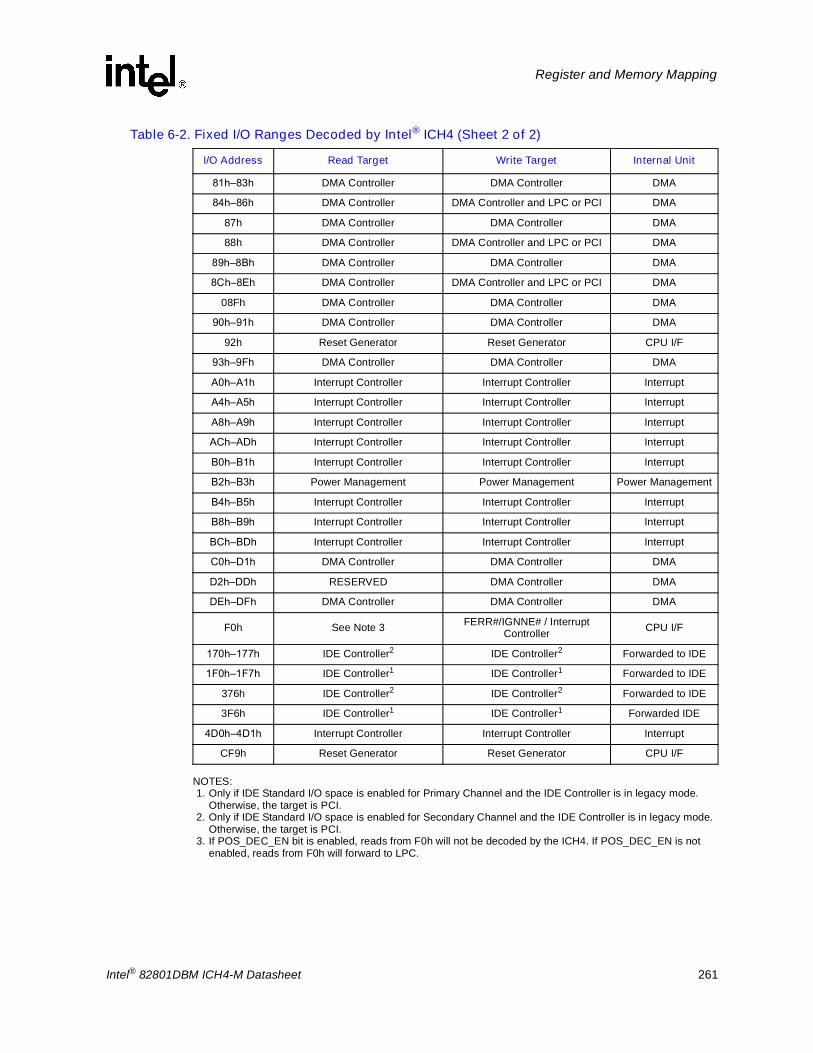
Intel® 82801DBM ICH4-M Datasheet 261
Register and Memory Mapping
NOTES:1. Only if IDE Standard I/O space is enabled for Primary Channel and the IDE Controller is in legacy mode.
Otherwise, the target is PCI.2. Only if IDE Standard I/O space is enabled for Secondary Channel and the IDE Controller is in legacy mode.
Otherwise, the target is PCI.3. If POS_DEC_EN bit is enabled, reads from F0h will not be decoded by the ICH4. If POS_DEC_EN is not
enabled, reads from F0h will forward to LPC.
81h�83h DMA Controller DMA Controller DMA
84h�86h DMA Controller DMA Controller and LPC or PCI DMA
87h DMA Controller DMA Controller DMA
88h DMA Controller DMA Controller and LPC or PCI DMA
89h�8Bh DMA Controller DMA Controller DMA
8Ch�8Eh DMA Controller DMA Controller and LPC or PCI DMA
08Fh DMA Controller DMA Controller DMA
90h�91h DMA Controller DMA Controller DMA
92h Reset Generator Reset Generator CPU I/F
93h�9Fh DMA Controller DMA Controller DMA
A0h�A1h Interrupt Controller Interrupt Controller Interrupt
A4h�A5h Interrupt Controller Interrupt Controller Interrupt
A8h�A9h Interrupt Controller Interrupt Controller Interrupt
ACh�ADh Interrupt Controller Interrupt Controller Interrupt
B0h�B1h Interrupt Controller Interrupt Controller Interrupt
B2h�B3h Power Management Power Management Power Management
B4h�B5h Interrupt Controller Interrupt Controller Interrupt
B8h�B9h Interrupt Controller Interrupt Controller Interrupt
BCh�BDh Interrupt Controller Interrupt Controller Interrupt
C0h�D1h DMA Controller DMA Controller DMA
D2h�DDh RESERVED DMA Controller DMA
DEh�DFh DMA Controller DMA Controller DMA
F0h See Note 3 FERR#/IGNNE# / Interrupt Controller CPU I/F
170h�177h IDE Controller2 IDE Controller2 Forwarded to IDE
1F0h�1F7h IDE Controller1 IDE Controller1 Forwarded to IDE
376h IDE Controller2 IDE Controller2 Forwarded to IDE
3F6h IDE Controller1 IDE Controller1 Forwarded IDE
4D0h�4D1h Interrupt Controller Interrupt Controller Interrupt
CF9h Reset Generator Reset Generator CPU I/F
Table 6-2. Fixed I/O Ranges Decoded by Intel® ICH4 (Sheet 2 of 2)
I/O Address Read Target Write Target Internal Unit

262 Intel® 82801DBM ICH4-M Datasheet
Register and Memory Mapping
6.3.2 Variable I/O Decode RangesTable 6-3 shows the Variable I/O Decode Ranges. They are set using Base Address Registers (BARs) or other configuration bits in the various PCI configuration spaces. The PNP software (PCI or ACPI) can use their configuration mechanisms to set and adjust these values.
When a cycle is detected on the hub interface, the ICH4 will positively decode the cycle. If the response is on the behalf of an LPC device, ICH4 will forward the cycle to the LPC I/F.
Refer to Table A-3 for a complete list of all variable I/O registers.
Warning: The Variable I/O Ranges should not be set to conflict with the Fixed I/O Ranges. Unpredictable results if the configuration software allows conflicts to occur. The ICH4 does not perform any checks for conflicts.
Table 6-3. Variable I/O Decode Ranges
Range Name Mappable Size (Bytes) Target
ACPI Anywhere in 64 kB I/O Space 64 Power Management
IDE Bus Master Anywhere in 64 kB I/O Space 16 IDE Unit
USB UHCI Controller #1 Anywhere in 64 kB I/O Space 32 USB Unit 1
SMBus Anywhere in 64 kB I/O Space 32 SMB Unit
AC�97 Audio Mixer Anywhere in 64 kB I/O Space 256 AC�97 Unit
AC�97 Bus Master Anywhere in 64 kB I/O Space 64 AC�97 Unit
AC�97 Modem Mixer Anywhere in 64 kB I/O Space 256 AC�97 Unit
TCO 96 Bytes above ACPI Base 32 TCO Unit
GPIO Anywhere in 64 kB I/O Space 64 GPIO Unit
Parallel Port 3 ranges in 64 kB I/O Space 8 LPC Peripheral
Serial Port 1 8 Ranges in 64 kB I/O Space 8 LPC Peripheral
Serial Port 2 8 Ranges in 64 kB I/O Space 8 LPC Peripheral
Floppy Disk Controller 2 Ranges in 64 kB I/O Space 8 LPC Peripheral
MIDI 4 Ranges in 64 kB I/O Space 2 LPC Peripheral
MSS 4 Ranges in 64 kB I/O Space 8 LPC Peripheral
SoundBlaster 2 Ranges in 64 kB I/O Space 32 LPC Peripheral
LAN Anywhere in 64 kB I/O Space 64 LAN Unit
USB UHCI Controller #2 Anywhere in 64 kB I/O Space 32 USB Unit 2
USB UHCI Controller #3 Anywhere in 64 kB I/O Space 32 USB Unit 3
LPC Generic 1 Anywhere in 64 kB I/O Space 128 LPC Peripheral
LPC Generic 2 Anywhere in 64 kB I/O Space 16 LPC Peripheral
Monitors 4:7 Anywhere in 64 kB I/O Space 16 LPC Peripheral or Trap on PCI
Native IDE Primary Command Anywhere in 64 kB I/O Space 8 IDE Unit
Native IDE Primary Control Anywhere in 64 kB I/O Space 4 IDE Unit
Native IDE Secondary Command Anywhere in 64 kB I/O Space 8 IDE Unit
Native IDE Secondary Control Anywhere in 64 kB I/O Space 4 IDE Unit

Intel® 82801DBM ICH4-M Datasheet 263
Register and Memory Mapping
6.4 Memory MapTable 6-4 shows (from the processor perspective) the memory ranges that the ICH4 will decode. Cycles that arrive from the hub interface that are not directed to any of the internal memory targets that decode directly from hub interface will be driven out on PCI. The ICH4 may then claim the cycle for it to be forwarded to LPC or claimed by the internal APIC. If subtractive decode is enabled, the cycle can be forwarded to LPC.
PCI cycles generated by an external PCI master will be positively decoded unless it falls in the PCI-PCI bridge forwarding range (those addresses are reserved for PCI peer-to-peer traffic). If the cycle is not in the I/O APIC or LPC ranges, it will be forwarded up the hub interface to the Host Controller. PCI masters can not access the memory ranges for functions that decode directly from Hub Interface.
Table 6-4. Memory Decode Ranges from Processor Perspective (Sheet 1 of 2)
Memory Range Target Dependency/Comments
0000 0000�000D FFFFh0010 0000h�TOM (Top of Memory)
Main Memory TOM registers in Host Controller
000E 0000�000F FFFFh FWH Bit 7 in FWH Decode Enable Register is set
FEC0 0000�FEC0 0100h I/O APIC inside ICH4
FFC0 0000�FFC7 FFFFhFF80 0000�FF87 FFFFh
FWH Bit 0 in FWH Decode Enable Register
FFC8 0000�FFCF FFFFhFF88 0000�FF8F FFFFh
FWH Bit 1 in FWH Decode Enable Register
FFD0 0000�FFD7 FFFFhFF90 0000�FF97 FFFFh
FWH Bit 2 in FWH Decode Enable Register is set
FFD8 0000�FFDF FFFFhFF98 0000�FF9F FFFFh
FWH Bit 3 in FWH Decode Enable Register is set
FFE0 000�FFE7 FFFFhFFA0 0000�FFA7 FFFFh
FWH Bit 4 in FWH Decode Enable Register is set
FFE8 0000�FFEF FFFFhFFA8 0000�FFAF FFFFh
FWH Bit 5 in FWH Decode Enable Register is set
FFF0 0000�FFF7 FFFFhFFB0 0000�FFB7 FFFFh
FWH Bit 6 in FWH Decode Enable Register is set.
FFF8 0000�FFFF FFFFhFFB8 0000�FFBF FFFFh
FWHAlways enabled.The top two 64 KB blocks of this range can be swapped, as described in Section 7.4.1.
FF70 0000�FF7F FFFFhFF30 0000�FF3F FFFFh
FWH Bit 3 in FWH Decode Enable 2 Register is set
FF60 0000�FF6F FFFFhFF20 0000�FF2F FFFFh
FWH Bit 2 in FWH Decode Enable 2 Register is set
FF50 0000�FF5F FFFFhFF10 0000�FF1F FFFFh
FWH Bit 1 in FWH Decode Enable 2 Register is set
FF40 0000�FF4F FFFFhFF00 0000�FF0F FFFFh
FWH Bit 0 in FWH Decode Enable 2 Register is set
4 kB anywhere in 4 GB range
Integrated LAN Controller
Enable via BAR in Device 29:Function 0 (Integrated LAN Controller)

264 Intel® 82801DBM ICH4-M Datasheet
Register and Memory Mapping
NOTES:1. These ranges are decoded directly from the hub interface. The memory cycles will not be seen on PCI. 2. Software must not attempt locks to memory mapped I/O ranges for USB EHCI and IDE Expansion. If
attempted, the lock is not honored, which means potential deadlock conditions may occur.
6.4.1 Boot-Block Update SchemeThe ICH4 supports a �top-block swap� mode that has the ICH4 swap the top block in the FWH (the boot block) with another location. This allows for safe update of the Boot Block (even if a power failure occurs). When the �TOP_SWAP� Enable bit is set, the ICH4 will invert A16 for cycles targeting FWH BIOS space. When this bit is 0, the ICH4 will not invert A16. This bit is automatically set to 0 by RTCRST#, but not by PCIRST#.
The scheme is based on the concept that the top block is reserved as the �boot� block, and the block immediately below the top block is reserved for doing boot-block updates.
The algorithm is:
1. Software copies the top block to the block immediately below the top2. Software checks that the copied block is correct. This could be done by performing a
checksum calculation.3. Software sets the TOP_SWAP bit. This will invert A16 for cycles going to the FWH. CPU
access to FFFF_0000 through FFFF_FFFF will be directed to FFFE_0000 through FFFE_FFFF in the FWH, and processor accesses to FFFE_0000 through FFFE_FFFF will be directed to FFFF_0000 through FFFF_FFFF.
4. Software erases the top block5. Software writes the new top block6. Software checks the new top block7. Software clears the TOP_SWAP bit
If a power failure occurs at any point after step 3, the system will be able to boot from the copy of the boot block that is stored in the block below the top. This is because the TOP_SWAP bit is backed in the RTC well.
Note: The top-block swap mode may be forced by an external strapping option (See Section 2.20.1). When top-block swap mode is forced in this manner, the TOP_SWAP bit cannot be cleared by software. A re-boot with the strap removed will be required to exit a forced top-block swap mode.
Note: Top-block swap mode only affects accesses to the FWH BIOS space, not feature space.
Note: The top-block swap mode has no effect on accesses below FFFE_0000.
1 kB anywhere in 4 GB range IDE Expansion2 Enable via standard PCI mechanism and bits in IDE I/O
Configuration Register (Device 31, Function 1)1 kB anywhere in 4 GB
rangeUSB EHCI
Controller1,2Enable via standard PCI mechanism (Device 29, Function 7)
All other PCI None
Table 6-4. Memory Decode Ranges from Processor Perspective (Sheet 2 of 2)
Memory Range Target Dependency/Comments

Intel® 82801DBM ICH4-M Datasheet 265
LAN Controller Registers (B1:D8:F0)
7 LAN Controller Registers (B1:D8:F0)
The ICH4 integrated LAN Controller appears to reside at PCI Device 8, Function 0 on the secondary side of the ICH4�s virtual PCI-to-PCI Bridge (See Section 5.1.2). This is typically Bus 1, but may be assigned a different number depending upon system configuration. The LAN Controller acts as both a master and a slave on the PCI bus. As a master, the LAN Controller interacts with the system main memory to access data for transmission or deposit received data. As a slave, some of the LAN Controller�s control structures are accessed by the host processor to read or write information to the on-chip registers. The processor also provides the LAN Controller with the necessary commands and pointers that allow it to process receive and transmit data.
7.1 PCI Configuration Registers (B1:D8:F0)Note: Registers that are not shown should be treated as Reserved (See Section 6.2 for details).
.
Table 7-1. LAN Controller PCI Configuration Register Address Map (LAN Controller�B1:D8:F0)
Offset Mnemonic Register Name Default Type
00�01h VID Vendor ID 8086h RO02�03h DID Device ID 103Ah RO04�05h PCICMD PCI Device Command Register 0000h R/W, RO
06�07h PCISTS PCI Device Status Register 0290h R/WC, RO08h REVID Revision ID See Note RO0Ah SCC Sub Class Code 00h RO0Bh BCC Base Class Code 02h RO
0Dh PMLT PCI Master Latency Timer 00h R/W0Eh HEADTYP Header Type 00h RO
10�13h CSR_MEM_BASE CSR Memory-Mapped Base Address 0008h R/W, RO14�17h CSR_IO_BASE CSR I/O-Mapped Base Address 0001h R/W, RO
2C�2Dh SVID Subsystem Vendor ID 0000h RO2E�2Fh SID Subsystem ID 0000h RO
34h CAP_PTR Capabilities Pointer DCh RO3Ch INT_LN Interrupt Line 00h R/W
3D INT_PN Interrupt Pin 01h RO3E MIN_GNT Minimum Grant 08h RO3F MAX_LAT Maximum Latency 38h RO
DCh CAP_ID Capability ID 01h RO
DDh NXT_PTR Next Item Pointer 00h RODE�DFh PM_CAP Power Management Capabilities 7E21h RO
E0�E1h PMCSR Power Management Control/Status 0000h R/WC, R/W, RO
E3 PCIDATA PCI Power Management Data 00h RO

266 Intel® 82801DBM ICH4-M Datasheet
LAN Controller Registers (B1:D8:F0)
NOTE: Refer to the ICH4 Specification Update for the value of the Revision ID Register.
7.1.1 VID�Vendor ID Register (LAN Controller�B1:D8:F0)Offset Address: 00�01h Attribute: RODefault Value: 8086h Size: 16 bits
7.1.2 DID�Device ID Register (LAN Controller�B1:D8:F0)Offset Address: 02�03h Attribute: RODefault Value: 103Ah Size: 16 bits
Bit Description
15:0 Vendor Identification Value � RO. This is a 16-bit value assigned to Intel.
Bit Description
15:0
Device Identification Value � RO. This is a 16-bit value assigned to the ICH4 integrated LAN Controller.
1. If the EEPROM is not present (or not properly programmed), reads to the Device ID return the default value of 103Ah
2. If the EEPROM is present (and properly programmed) and if the value of Word 23h is not 0000f or FFFFh, the Device ID is loaded from the EEPROM, Word 23h after the hardware reset. (See Section 7.1.14 for details)

Intel® 82801DBM ICH4-M Datasheet 267
LAN Controller Registers (B1:D8:F0)
7.1.3 PCICMD�PCI Command Register (LAN Controller�B1:D8:F0)Offset Address: 04�05h Attribute: R/W, RODefault Value: 0000h Size: 16 bits
Bit Description
15:10 Reserved
9 Fast Back to Back Enable (FBE) � RO. Hardwired to 0. The integrated LAN* Controller will not run fast back-to-back PCI cycles.
8SERR# Enable (SERR_EN) � R/W. 0 = Disable.1 = Enable. Allow SERR# to be asserted.
7 Wait Cycle Control (WCC) � RO. Hardwired to 0. Not implemented.
6
Parity Error Response (PER) � R/W0 = The LAN Controller will ignore PCI parity errors.1 = The integrated LAN Controller will take normal action when a PCI parity error is detected and
will enable generation of parity on the hub interface.
5 VGA Palette Snoop (VPS) � RO. Hardwired to 0. Not Implemented.
4Memory Write and Invalidate Enable (MWIE) � R/W.0 = Disable. The LAN* Controller will not use the Memory Write and Invalidate command.1 = Enable.
3 Special Cycle Enable (SCE) � RO. Hardwired to 0. The LAN Controller ignores special cycles.
2Bus Master Enable (BME) � R/W. 0 = Disable.1 = Enable. The ICH4�s integrated may function as a PCI bus master.
1Memory Space Enable (MSE) � R/W.0 = Disable.1 = Enable. The ICH4�s integrated LAN Controller will respond to the memory space accesses.
0I/O Space Enable (IOSE) � R/W.0 = Disable.1 = Enable. The ICH4�s integrated LAN Controller will respond to the I/O space accesses.

268 Intel® 82801DBM ICH4-M Datasheet
LAN Controller Registers (B1:D8:F0)
7.1.4 PCISTS�PCI Status Register (LAN Controller�B1:D8:F0)Offset Address: 06�07h Attribute: R/WC, RODefault Value: 0290h Size: 16 bits
Bit Description
15
Detected Parity Error (DPE) � R/WC.0 = This bit is cleared by writing a 1 to the bit location.1 = The ICH4�s integrated LAN* Controller has detected a parity error on the PCI bus (will be set
even if Parity Error Response is disabled in the PCI Command register).
14
Signaled System Error (SSE) � R/WC.0 = This bit is cleared by writing a 1 to the bit location.1 = The ICH4�s integrated LAN Controller has asserted SERR#. (SERR# can be routed to cause
NMI, SMI# or interrupt.
13Master Abort Status (MAS) � R/WC.0 = This bit is cleared by writing a 1 to the bit location.1 = The ICH4�s integrated LAN Controller (as a PCI master) has generated a master abort.
12Received Target Abort (RTA) � R/WC.0 = This bit is cleared by writing a 1 to the bit location.1 = The ICH4�s integrated LAN Controller (as a PCI master) has received a target abort.
11 Signaled Target Abort (STA) � RO. Hardwired to 0. The device will never signal Target Abort.
10:9DEVSEL# Timing Status (DEV_STS) �RO. 01h = Medium timing.
8
Data Parity Error Detected (DPED) � R/WC.0 = This bit is cleared by writing a 1 to the bit location.1 = All of the following three conditions have been met:1. The LAN Controller is acting as bus master2. The LAN Controller has asserted PERR# (for reads) or detected PERR# asserted (for writes)3. The Parity Error Response bit in the LAN Controller�s PCI Command Register is set.
7 Fast Back to Back Capable (FB2BC) � RO. Hardwired to 1. The device can accept fast back-to-back transactions.
6 User Definable Features (UDF) � RO. Hardwired to 0. Not implemented.
5 66 MHz Capable (66MHZ_CAP) � RO. Hardwired to 0. The device does not support 66 MHz PCI.
4
Capabilities List (CAP_LIST) � RO.0 = The EEPROM indicates that the integrated LAN controller does not support PCI Power
Management.1 = The EEPROM indicates that the integrated LAN controller supports PCI Power Management.
3:0 Reserved

Intel® 82801DBM ICH4-M Datasheet 269
LAN Controller Registers (B1:D8:F0)
7.1.5 REVID�Revision ID Register (LAN Controller�B1:D8:F0)Offset Address: 08h Attribute: RODefault Value: See Note Size: 8 bits
NOTE: Refer to the ICH4 Specification Update for the value of the Revision ID Register.
7.1.6 SCC�Sub-Class Code Register (LAN Controller�B1:D8:F0)Offset Address: 0Ah Attribute: RODefault Value: 00h Size: 8 bits
7.1.7 BCC�Base-Class Code Register (LAN Controller�B1:D8:F0)Offset Address: 0Bh Attribute: RODefault Value: 02h Size: 8 bits
7.1.8 CLS�Cache Line Size Register (LAN Controller�B1:D8:F0)Offset Address: 0Ch Attribute: R/WDefault Value: 00h Size: 8 bits
Bit Description
7:0Revision Identification Value � RO. This 8-bit value indicates the revision number for the integrated LAN* Controller. The three least significant bits in this register may be overridden by the ID and REV ID fields in the EEPROM.
Bit Description
7:0 Sub Class Code � RO. 8-bit value that specifies the sub-class of the device as an Ethernet controller.
Bit Description
7:0 Base Class Code � RO. 8-bit value that specifies the base class of the device as a network controller.
Bit Description
7:5 Reserved
4:3
Cache Line Size (CLS) � R/W.00 = Memory Write and Invalidate (MWI) command will not be used by the integrated LAN* Controller.01 = MWI command will be used with Cache Line Size set to 8 DWORDs (only set if a value of 08h is
written to this register).10 = MWI command will be used with Cache Line Size set to 16 DWORDs (only set if a value of 10h
is written to this register).11 = Invalid. MWI command will not be used.
2:0 Reserved

270 Intel® 82801DBM ICH4-M Datasheet
LAN Controller Registers (B1:D8:F0)
7.1.9 PMLT�PCI Master Latency Timer Register (LAN Controller�B1:D8:F0)Offset Address: 0Dh Attribute: R/WDefault Value: 00h Size: 8 bits
7.1.10 HEADTYP�Header Type Register (LAN Controller�B1:D8:F0)Offset Address: 0Eh Attribute: RODefault Value: 00h Size: 8 bits
7.1.11 CSR_MEM_BASE CSR � Memory-Mapped Base Address Register (LAN Controller�B1:D8:F0)Offset Address: 10�13h Attribute: R/W, RODefault Value: 0000 0008h Size: 32 bits
Note: The ICH4�s integrated LAN Controller requires one BAR for memory mapping. Software determines which BAR (memory or I/O) is used to access the Lan Controller�s CSR registers.
Bit Description
7:3 Master Latency Timer Count (MLTC) � R/W. Defines the number of PCI clock cycles that the integrated LAN Controller may own the bus while acting as bus master.
2:0 Reserved
Bit Description
7 Multi-Function Device � RO. Hardwired to 0 to indicate a single function device.
6:0 Header Type � RO. This 7-bit field identifies the header layout of the configuration space as an Ethernet controller.
Bit Description
31:12 Base Address � R/W. Upper 20 bits of the base address provides 4 KB of memory-Mapped space for the LAN* Controller�s Control/Status Registers.
11:4 Reserved
3 Prefetchable � RO. Hardwired to 0 to indicate that this is not a pre-fetchable memory-Mapped address range.
2:1 Type � RO. Hardwired to 00b to indicate the memory-Mapped address range may be located anywhere in 32-bit address space.
0 Memory Space Indicator � RO. Hardwired to 0 to indicate that this base address maps to memory space.

Intel® 82801DBM ICH4-M Datasheet 271
LAN Controller Registers (B1:D8:F0)
7.1.12 CSR_IO_BASE � CSR I/O-Mapped Base Address Register (LAN Controller�B1:D8:F0)Offset Address: 14�17h Attribute: R/W, RODefault Value: 0000 0001h Size: 32 bits
Note: The ICH4�s integrated LAN Controller requires one BAR for memory mapping. Software determines which BAR (memory or I/O) is used to access the Lan Controller�s CSR registers.
7.1.13 SVID � Subsystem Vendor ID (LAN Controller�B1:D8:F0)Offset Address: 2C�2D Attribute: RODefault Value: 0000h Size: 16 bits
7.1.14 SID � Subsystem ID (LAN Controller�B1:D8:F0)Offset Address: 2E�2Fh Attribute: RODefault Value: 0000h Size: 16 bits
Note: The ICH4�s integrated LAN Controller provides support for configurable Subsystem ID and Subsystem Vendor ID fields. After reset, the LAN Controller automatically reads addresses Ah through Ch, and 23h of the EEPROM. The LAN Controller checks bits 15:13 in the EEPROM word Ah, and functions according to Table 7-2.
NOTE:1. Refer to the ICH4 Specification Update for the value of the Revision ID Register.2. The Device ID is loaded from Word 23h only if the value of Word 23h is not 0000h or FFFFh.
Bit Description
31:16 Reserved
15:6 Base Address � R/W. Provides 64 bytes of I/O-Mapped address space for the LAN Controller�s Control/Status Registers.
5:1 Reserved
0 I/O Space Indicator � RO. Hardwired to 1 to indicate that this base address maps to I/O space.
Bit Description
15:0 Subsystem Vendor ID (SVID) � RO. (see Section 7.1.14 for details)
Bit Description
15:0 Subsystem ID (SID) � RO.
Table 7-2. Configuration of Subsystem ID and Subsystem Vendor ID via EEPROM
Bits 15:14 Bit 13 Device ID Vendor ID Revision ID Subsystem ID Subsystem Vendor ID
11b, 10b, 00b X 103Ah 8086h Note 1 0000h 0000h
01b 0b Word 23h 8086h Note 1 Word Bh Word Ch
01b 1b Word 23h Word Ch REVID + Word Ah, bits 10:8 Word Bh Word Ch

272 Intel® 82801DBM ICH4-M Datasheet
LAN Controller Registers (B1:D8:F0)
7.1.15 CAP_PTR � Capabilities Pointer (LAN Controller�B1:D8:F0)Offset Address: 34h Attribute: RODefault Value: DCh Size: 8 bits
7.1.16 INT_LN � Interrupt Line Register (LAN Controller�B1:D8:F0)Offset Address: 3Ch Attribute: R/WDefault Value: 00h Size: 8 bits
7.1.17 INT_PN � Interrupt Pin Register (LAN Controller�B1:D8:F0)Offset Address: 3Dh Attribute: RODefault Value: 01h Size: 8 bits
7.1.18 MIN_GNT � Minimum Grant Register (LAN Controller�B1:D8:F0)Offset Address: 3Eh Attribute: RODefault Value: 08h Size: 8 bits
Bit Description
7:0 Capabilities Pointer (CAP_PTR) � RO. Hardwired to DCh; indicates the offset within configuration space for the location of the Power Management registers.
Bit Description
7:0 Interrupt Line (INT_LN) � R/W. Identifies the system interrupt line to which the LAN Controller�s PCI interrupt request pin (as defined in the Interrupt Pin Register) is routed.
Bit Description
7:0
Interrupt Pin (INT_PN) � RO. Hardwired to 01h to indicate that the LAN Controller�s interrupt request is connected to PIRQA#. However, in the ICH4 implementation, when the LAN Controller interrupt is generated PIRQ[E]# will go active, not PIRQ[A]#. Note that if the PIRQ[E]# signal is used as a GPIO, the external visibility will be lost (though PIRQ[E]# will still go active internally).
Bit Description
7:0 Minimum Grant (MIN_GNT) � RO. This field indicates the amount of time (in increments of 0.25 s) that the LAN Controller needs to retain ownership of the PCI bus when it initiates a transaction.

Intel® 82801DBM ICH4-M Datasheet 273
LAN Controller Registers (B1:D8:F0)
7.1.19 MAX_LAT � Maximum Latency Register (LAN Controller�B1:D8:F0)Offset Address: 3Fh Attribute: RODefault Value: 38h Size: 8 bits
7.1.20 CAP_ID � Capability ID Register (LAN Controller�B1:D8:F0)Offset Address: DCh Attribute: RODefault Value: 01h Size: 8 bits
7.1.21 NXT_PTR � Next Item Pointer (LAN Controller�B1:D8:F0)Offset Address: DDh Attribute: RODefault Value: 00h Size: 8 bits
Bit Description
7:0 Maximum Latency (MAX_LAT) � RO. This field defines how often (in increments of 0.25 s) the LAN Controller needs to access the PCI bus.
Bit Description
7:0 Capability ID (CAP_ID) � RO. Hardwired to 01h to indicate that the ICH4�s integrated LAN Controller supports PCI Power Management.
Bit Description
7:0 Next Item Pointer (NXT_PTR) � RO. Hardwired to 00b to indicate that power management is the last item in the Capabilities list.
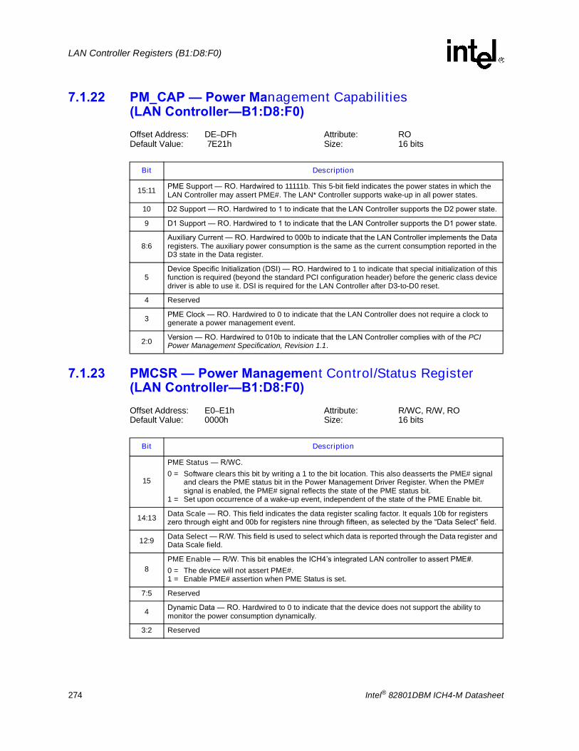
274 Intel® 82801DBM ICH4-M Datasheet
LAN Controller Registers (B1:D8:F0)
7.1.22 PM_CAP � Power Management Capabilities (LAN Controller�B1:D8:F0)Offset Address: DE�DFh Attribute: RODefault Value: 7E21h Size: 16 bits
7.1.23 PMCSR � Power Management Control/Status Register (LAN Controller�B1:D8:F0)Offset Address: E0�E1h Attribute: R/WC, R/W, RODefault Value: 0000h Size: 16 bits
Bit Description
15:11 PME Support � RO. Hardwired to 11111b. This 5-bit field indicates the power states in which the LAN Controller may assert PME#. The LAN* Controller supports wake-up in all power states.
10 D2 Support � RO. Hardwired to 1 to indicate that the LAN Controller supports the D2 power state.
9 D1 Support � RO. Hardwired to 1 to indicate that the LAN Controller supports the D1 power state.
8:6Auxiliary Current � RO. Hardwired to 000b to indicate that the LAN Controller implements the Data registers. The auxiliary power consumption is the same as the current consumption reported in the D3 state in the Data register.
5Device Specific Initialization (DSI) � RO. Hardwired to 1 to indicate that special initialization of this function is required (beyond the standard PCI configuration header) before the generic class device driver is able to use it. DSI is required for the LAN Controller after D3-to-D0 reset.
4 Reserved
3 PME Clock � RO. Hardwired to 0 to indicate that the LAN Controller does not require a clock to generate a power management event.
2:0 Version � RO. Hardwired to 010b to indicate that the LAN Controller complies with of the PCI Power Management Specification, Revision 1.1.
Bit Description
15
PME Status � R/WC. 0 = Software clears this bit by writing a 1 to the bit location. This also deasserts the PME# signal
and clears the PME status bit in the Power Management Driver Register. When the PME# signal is enabled, the PME# signal reflects the state of the PME status bit.
1 = Set upon occurrence of a wake-up event, independent of the state of the PME Enable bit.
14:13 Data Scale � RO. This field indicates the data register scaling factor. It equals 10b for registers zero through eight and 00b for registers nine through fifteen, as selected by the �Data Select� field.
12:9 Data Select � R/W. This field is used to select which data is reported through the Data register and Data Scale field.
8PME Enable � R/W. This bit enables the ICH4�s integrated LAN controller to assert PME#.0 = The device will not assert PME#.1 = Enable PME# assertion when PME Status is set.
7:5 Reserved
4 Dynamic Data � RO. Hardwired to 0 to indicate that the device does not support the ability to monitor the power consumption dynamically.
3:2 Reserved

Intel® 82801DBM ICH4-M Datasheet 275
LAN Controller Registers (B1:D8:F0)
7.1.24 PCIDATA � PCI Power Management Data Register (LAN Controller�B1:D8:F0)Offset Address: E3h Attribute: RODefault Value: 00h Size: 8 bits
Note: The data register is an 8-bit read only register that provides a mechanism for the ICH4�s integrated LAN Controller to report state dependent maximum power consumption and heat dissipation. The value reported in this register depends on the value written to the Data Select field in the PMCSR register. The power measurements defined in this register have a dynamic range of 0 W to 2.55 W with 0.01 W resolution, scaled according to the Data Scale field in the PMCSR. The structure of the Data Register is given in Table 7-3.
1:0
Power State � R/W. This 2-bit field is used to determine the current power state of the integrated LAN Controller, and to put it into a new power state. The definition of the field values is as follows:00 = D001 = D110 = D211 = D3
Bit Description
Bit Description
7:0 State dependent power consumption and heat dissipation data.
Table 7-3. Data Register Structure
Data Select Data Scale Data Reported
0 2 D0 Power Consumption
1 2 D1 Power Consumption
2 2 D2 Power Consumption
3 2 D3 Power Consumption
4 2 D0 Power Dissipated
5 2 D1 Power Dissipated
6 2 D2 Power Dissipated
7 2 D3 Power Dissipated
8 2 Common Function Power Dissipated
9�15 0 Reserved
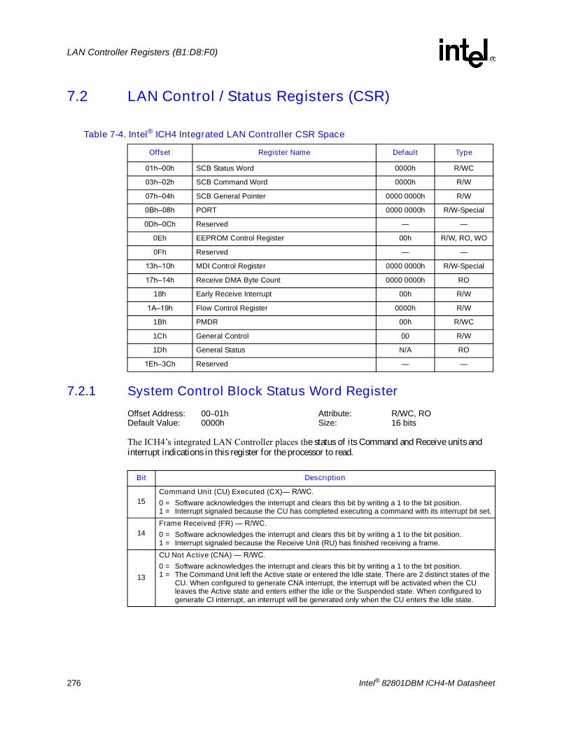
276 Intel® 82801DBM ICH4-M Datasheet
LAN Controller Registers (B1:D8:F0)
7.2 LAN Control / Status Registers (CSR)
7.2.1 System Control Block Status Word RegisterOffset Address: 00�01h Attribute: R/WC, RODefault Value: 0000h Size: 16 bits
The ICH4�s integrated LAN Controller places the status of its Command and Receive units and interrupt indications in this register for the processor to read.
Table 7-4. Intel® ICH4 Integrated LAN Controller CSR Space
Offset Register Name Default Type
01h�00h SCB Status Word 0000h R/WC
03h�02h SCB Command Word 0000h R/W
07h�04h SCB General Pointer 0000 0000h R/W
0Bh�08h PORT 0000 0000h R/W-Special
0Dh�0Ch Reserved � �
0Eh EEPROM Control Register 00h R/W, RO, WO
0Fh Reserved � �
13h�10h MDI Control Register 0000 0000h R/W-Special
17h�14h Receive DMA Byte Count 0000 0000h RO
18h Early Receive Interrupt 00h R/W
1A�19h Flow Control Register 0000h R/W
1Bh PMDR 00h R/WC
1Ch General Control 00 R/W
1Dh General Status N/A RO
1Eh�3Ch Reserved � �
Bit Description
15Command Unit (CU) Executed (CX)� R/WC.0 = Software acknowledges the interrupt and clears this bit by writing a 1 to the bit position.1 = Interrupt signaled because the CU has completed executing a command with its interrupt bit set.
14Frame Received (FR) � R/WC. 0 = Software acknowledges the interrupt and clears this bit by writing a 1 to the bit position.1 = Interrupt signaled because the Receive Unit (RU) has finished receiving a frame.
13
CU Not Active (CNA) � R/WC.0 = Software acknowledges the interrupt and clears this bit by writing a 1 to the bit position.1 = The Command Unit left the Active state or entered the Idle state. There are 2 distinct states of the
CU. When configured to generate CNA interrupt, the interrupt will be activated when the CU leaves the Active state and enters either the Idle or the Suspended state. When configured to generate CI interrupt, an interrupt will be generated only when the CU enters the Idle state.

Intel® 82801DBM ICH4-M Datasheet 277
LAN Controller Registers (B1:D8:F0)
12
Receive Not Ready (RNR) � R/WC. 0 = Software acknowledges the interrupt and clears this bit by writing a 1 to the bit position.1 = Interrupt signaled because the Receive Unit left the Ready state. This may be caused by an RU
Abort command, a no resources situation, or set suspend bit due to a filled Receive Frame Descriptor.
11
Management Data Interrupt (MDI) � R/WC. 0 = Software acknowledges the interrupt and clears this bit by writing a 1 to the bit position.1 = Set when a Management Data Interface read or write cycle has completed. The management
data interrupt is enabled through the interrupt enable bit (bit 29 in the Management Data Interface Control register in the CSR).
10Software Interrupt (SWI) � R/WC.0 = Software acknowledges the interrupt and clears this bit by writing a 1 to the bit position.1 = Set when software generates an interrupt.
9Early Receive (ER) � R/WC.0 = Software acknowledges the interrupt and clears this bit by writing a 1 to the bit position.1 = Indicates the occurrence of an Early Receive Interrupt.
8Flow Control Pause (FCP) � R/WC.0 = Software acknowledges the interrupt and clears this bit by writing a 1 to the bit position.1 = Indicates Flow Control Pause interrupt.
7:6
Command Unit Status (CUS) � RO.00 = Idle01 = Suspended10 = LPQ (Low Priority Queue) active11 = HPQ (High Priority Queue) active
5:2
Receive Unit Status (RUS) �RO.0000 = Idle1000 = Reserved0001 = Suspended1001 = Suspended with no more RBDs0010 = No Resources1010 = No resources due to no more RBDs0011 = Reserved1011 = Reserved0100 = Ready1100 = Ready with no RBDs present0101 = Reserved1101 = Reserved0110 = Reserved1110 = Reserved0111 = Reserved1111 = Reserved
1:0 Reserved
Bit Description
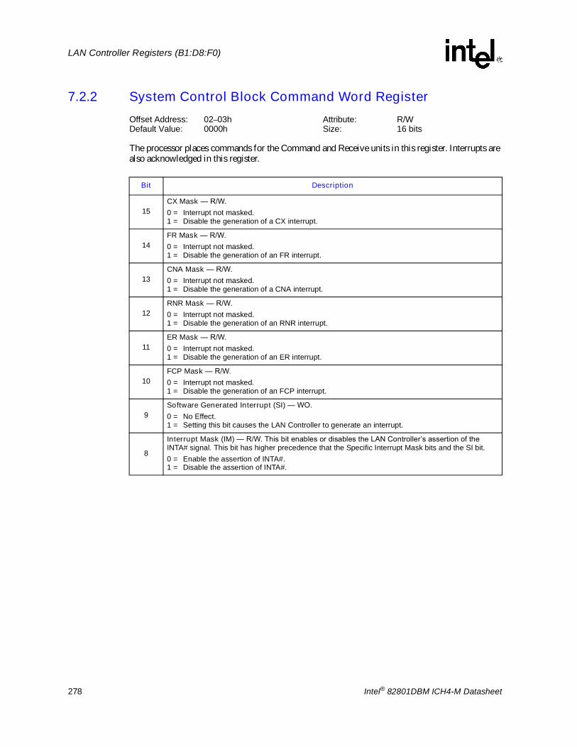
278 Intel® 82801DBM ICH4-M Datasheet
LAN Controller Registers (B1:D8:F0)
7.2.2 System Control Block Command Word RegisterOffset Address: 02�03h Attribute: R/WDefault Value: 0000h Size: 16 bits
The processor places commands for the Command and Receive units in this register. Interrupts are also acknowledged in this register.
Bit Description
15CX Mask � R/W.0 = Interrupt not masked.1 = Disable the generation of a CX interrupt.
14FR Mask � R/W.0 = Interrupt not masked.1 = Disable the generation of an FR interrupt.
13CNA Mask � R/W.0 = Interrupt not masked.1 = Disable the generation of a CNA interrupt.
12RNR Mask � R/W.0 = Interrupt not masked.1 = Disable the generation of an RNR interrupt.
11ER Mask � R/W.0 = Interrupt not masked.1 = Disable the generation of an ER interrupt.
10FCP Mask � R/W.0 = Interrupt not masked.1 = Disable the generation of an FCP interrupt.
9Software Generated Interrupt (SI) � WO. 0 = No Effect.1 = Setting this bit causes the LAN Controller to generate an interrupt.
8
Interrupt Mask (IM) � R/W. This bit enables or disables the LAN Controller�s assertion of the INTA# signal. This bit has higher precedence that the Specific Interrupt Mask bits and the SI bit.0 = Enable the assertion of INTA#.1 = Disable the assertion of INTA#.
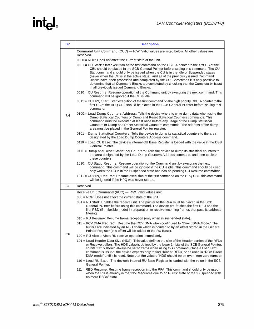
Intel® 82801DBM ICH4-M Datasheet 279
LAN Controller Registers (B1:D8:F0)
7:4
Command Unit Command (CUC) � R/W. Valid values are listed below. All other values are Reserved.0000 = NOP: Does not affect the current state of the unit.0001 = CU Start: Start execution of the first command on the CBL. A pointer to the first CB of the
CBL should be placed in the SCB General Pointer before issuing this command. The CU Start command should only be issued when the CU is in the Idle or Suspended states (never when the CU is in the active state), and all of the previously issued Command Blocks have been processed and completed by the CU. Sometimes it is only possible to determine that all Command Blocks are completed by checking that the Complete bit is set in all previously issued Command Blocks.
0010 = CU Resume: Resume operation of the Command unit by executing the next command. This command will be ignored if the CU is idle.
0011 = CU HPQ Start: Start execution of the first command on the high priority CBL. A pointer to the first CB of the HPQ CBL should be placed in the SCB General POinter before issuing this command.
0100 = Load Dump Counters Address: Tells the device where to write dump data when using the Dump Statistical Counters or Dump and Reset Statistical Counters commands. This command must be executed at least once before any usage of the Dump Statistical Counters or Dump and Reset Statistical Counters commands. The address of the dump area must be placed in the General Pointer register.
0101 = Dump Statistical Counters: Tells the device to dump its statistical counters to the area designated by the Load Dump Counters Address command.
0110 = Load CU Base: The device�s internal CU Base Register is loaded with the value in the CSB General Pointer.
0111 = Dump and Reset Statistical Counters: Tells the device to dump its statistical counters to the area designated by the Load Dump Counters Address command, and then to clear these counters.
1010 = CU Static Resume: Resume operation of the Command unit by executing the next command. This command will be ignored if the CU is idle. This command should be used only when the CU is in the Suspended state and has no pending CU Resume commands.
1011 = CU HPQ Resume: Resume execution of the first command on the HPQ CBL. this command will be ignored if the HPQ was never started.
3 Reserved
2:0
Receive Unit Command (RUC) � R/W. Valid values are:000 = NOP: Does not affect the current state of the unit.001 = RU Start: Enables the receive unit. The pointer to the RFA must be placed in the SCB
General POinter before using this command. The device pre-fetches the first RFD and the first RBD (if in flexible mode) in preparation to receive incoming frames that pass its address filtering.
010 = RU Resume: Resume frame reception (only when in suspended state).011 = RCV DMA Redirect: Resume the RCV DMA when configured to �Direct DMA Mode.� The
buffers are indicated by an RBD chain which is pointed to by an offset stored in the General Pointer Register (this offset will be added to the RU Base).
100 = RU Abort: Abort RU receive operation immediately.101 = Load Header Data Size (HDS): This value defines the size of the Header portion of the RFDs
or Receive buffers. The HDS value is defined by the lower 14 bits of the SCB General Pointer, so bits 31:15 should always be set to zeros when using this command. Once a Load HDS command is issued, the device expects only to find Header RFDs, or be used in �RCV Direct DMA mode� until it is reset. Note that the value of HDS should be an even, non-zero number.
110 = Load RU Base: The device�s internal RU Base Register is loaded with the value in the SCB General Pointer.
111 = RBD Resume: Resume frame reception into the RFA. This command should only be used when the RU is already in the �No Resources due to no RBDs� state or the �Suspended with no more RBDs� state.
Bit Description

280 Intel® 82801DBM ICH4-M Datasheet
LAN Controller Registers (B1:D8:F0)
7.2.3 System Control Block General Pointer RegisterOffset Address: 04�07h Attribute: R/WDefault Value: 0000 0000h Size: 32 bits
7.2.4 PORT RegisterOffset Address: 08�0Bh Attribute: R/W (special)Default Value: 0000 0000h Size: 32 bits
The PORT interface allows the processor to reset the ICH4�s internal LAN Controller, or perform an internal self test. The PORT DWORD may be written as a 32-bit entity, two 16-bit entities, or four 8-bit entities. The LAN Controller will only accept the command after the high byte (offset 0Bh) is written; therefore, the high byte must be written last.
Bit Description
15:0 SCB General Pointer � R/W. The SCB General Pointer register is programmed by software to point to various data structures in main memory depending on the current SCB Command word.
Bit Description
31:4Pointer Field � R/W (special). A 16-byte aligned address must be written to this field when issuing a Self-Test command to the PORT interface.The results of the Self Test will be written to the address specified by this field.
3:0
PORT Function Selection � R/W (special). Valid values are listed below. All other values are Reserved.0000 = PORT Software Reset: Completely resets the LAN Controller (all CSR and PCI registers).
This command should not be used when the device is active. If a PORT Software Reset is desired, software should do a Selective Reset (described below), wait for the PORT register to be cleared (completion of the Selective Reset), and then issue the PORT Software Reset command. Software should wait approximately 10 s after issuing this command before attempting to access the LAN Controller�s registers again.
0001 = Self Test: The Self-Test begins by issuing an internal Selective Reset followed by a general internal self-test of the LAN Controller. The results of the self-test are written to memory at the address specified in the Pointer field of this register. The format of the self-test result is shown in Table 7-5. After completing the self-test and writing the results to memory, the LAN Controller will execute a full internal reset and will re-initialize to the default configuration. Self-Test does not generate an interrupt of similar indicator to the host processor upon completion.
0010 = Selective Reset: Sets the CU and RU to the Idle state, but otherwise maintains the current configuration parameters (RU and CU Base, HDSSize, Error Counters, Configure information and Individual/Multicast Addresses are preserved). Software should wait approximately 10 s after issuing this command before attempting to access the LAN* Controller�s registers again.

Intel® 82801DBM ICH4-M Datasheet 281
LAN Controller Registers (B1:D8:F0)
7.2.5 EEPROM Control RegisterOffset Address: 0Eh Attribute: RO, R/W, WODefault Value: 00h Size: 8 bits
The EEPROM Control Register is a 16-bit field that enables a read from and a write to the external EEPROM.
Table 7-5. Self-Test Results Format
Bit Description
31:13 Reserved
12General Self-Test Result � R/W (special).0 = Pass1 = Fail
11:6 Reserved
5
Diagnose Result � R/W (special). This bit provides the result of an internal diagnostic test of the Serial Subsystem.0 = Pass1 = Fail
4 Reserved
3
Register Result � R/W (special). This bit provides the result of a test of the internal Parallel Subsystem registers.0 = Pass1 = Fail
2
ROM Content Result � R/W (special). This bit provides the result of a test of the internal microcode ROM.0 = Pass1 = Fail
1:0 Reserved
Bit Description
7:4 Reserved
3EEPROM Serial Data Out (EEDO)� RO. Note that this bit represents "Data Out" from the perspective of the EEPROM device. This bit contains the value read from the EEPROM when performing read operations.
2EEPROM Serial Data In (EEDI)� WO. Note that this bit represents "Data In" from the perspective of the EEPROM device. The value of this bit is written to the EEPROM when performing write operations.
1
EEPROM Chip Select (EECS)� R/W.0 = Drives the ICH4�s EE_CS signal low, to disable the EEPROM. this bit must be set to 0 for a
minimum of 1 s between consecutive instruction cycles.1 = Drives the ICH4�s EE_CS signal high, to enable the EEPROM.
0
EEPROM Serial Clock (EESK)� R/W. Toggling this bit, clocks data into or out of the EEPROM. Software must ensure that this bit is toggled at a rate that meets the EEPROM component�s minimum clock frequency specification.0 = Drives the ICH4�s EE_SHCLK signal low.1 = Drives the ICH4�s EE_SHCLK signal high.

282 Intel® 82801DBM ICH4-M Datasheet
LAN Controller Registers (B1:D8:F0)
7.2.6 Management Data Interface (MDI) Control RegisterOffset Address: 10�13h Attribute: R/W (special)Default Value: 0000 0000h Size: 32 bits
The Management Data Interface (MDI) Control register is a 32-bit field and is used to read and write bits from the LAN Connect component. This register may be written as a 32-bit entity, two 16-bit entities, or four 8-bit entities. The LAN Controller will only accept the command after the high byte (offset 13h) is written, therefore the high byte must be written last.
Bit Description
31:30 These bits are reserved and should be set to 00b.
29Interrupt Enable � R/W. 0 = Disable.1 = Enables the LAN Controller to assert an interrupt to indicate the end of an MDI cycle.
28Ready � R/W. 0 = Expected to be reset by software at the same time the command is written.1 = Set by the LAN Controller at the end of an MDI transaction.
27:26
Opcode � R/W. These bits define the opcode: 00 = Reserved01 = MDI write10 = MDI read11 = Reserved
25:21 LAN Connect Address � R/W. This field of bits contains the LAN Connect address.
20:16 LAN Connect Register Address � R/W. This field of bits contains the LAN Connect Register Address.
15:0
Data � R/W. In a write command, software places the data bits in this field, and the LAN* Controller transfers the data to the external LAN Connect component. During a read command, the LAN Controller reads these bits serially from the LAN Connect, and software reads the data from this location.

Intel® 82801DBM ICH4-M Datasheet 283
LAN Controller Registers (B1:D8:F0)
7.2.7 Receive DMA Byte Count RegisterOffset Address: 14�17h Attribute: RODefault Value: 0000 0000h Size: 32 bits
7.2.8 Early Receive Interrupt RegisterOffset Address: 18h Attribute: R/WDefault Value: 00h Size: 8 bits
The Early Receive Interrupt register allows the internal LAN Controller to generate an early interrupt depending on the length of the frame. The LAN Controller will generate an interrupt at the end of the frame regardless of whether or not Early Receive Interrupts are enabled.
Note: It is recommended that software not utilize this register unless receive interrupt latency is a critical performance issue in that particular software environment. Using this feature may reduce receive interrupt latency, but will also result in the generation of more interrupts, that can degrade system efficiency and performance in some environments.
Bit Description
31:0 Receive DMA Byte Count � RO. Keeps track of how many bytes of receive data have been passed into host memory via DMA.
Bit Description
7:0
Early Receive Count � R/W. When some non-zero value x is programmed into this register, the LAN controller will set the ER bit in the SCB Status Word Register and assert INTA# when the byte count indicates that there are x quad-words remaining to be received in the current frame (based on the Type/Length field of the received frame). No Early Receive interrupt will be generated if a value of 00h (the default value) is programmed into this register.

284 Intel® 82801DBM ICH4-M Datasheet
LAN Controller Registers (B1:D8:F0)
7.2.9 Flow Control RegisterOffset Address: 19�1Ah Attribute: RO, R/W (special)Default Value: h Size: 16 bits
Bit Description
15:13 Reserved
12FC Paused Low � RO.0 = Cleared when the FC timer reaches zero, or a Pause frame is received.1 = Set when the LAN Controller receives a Pause Low command with a value greater than zero.
11
FC Paused � RO.0 = Cleared when the FC timer reaches zero.1 = Set when the LAN Controller receives a Pause command regardless of its cause (FIFO
reaching Flow Control Threshold, fetching a Receive Frame Descriptor with its Flow Control Pause bit set, or software writing a 1 to the Xoff bit).
10FC Full � RO.0 = Cleared when the FC timer reaches zero.1 = Set when the LAN Controller sends a Pause command with a value greater than zero.
9
Xoff � R/W (special). This bit should only be used if the LAN Controller is configured to operate with IEEE frame-based flow control.0 = This bit can only be cleared by writing a 1 to the Xon bit (bit 8 in this register).1 = Writing a 1 to this bit forces the Xoff request to 1 and causes the LAN Controller to behave as if
the FIFO extender is full. This bit will also be set to 1 when an Xoff request due to an �RFD Xoff� bit.
8
Xon � WO. This bit should only be used if the LAN Controller is configured to operate with IEEE frame-based flow control.0 = This bit always returns 0 on reads.1 = Writing a 1 to this bit resets the Xoff request to the LAN Controller, clearing bit 9 in this register.
7:3 Reserved
2:0
Flow Control Threshold � R/W. The LAN Controller can generate a Flow Control Pause frame when its Receive FIFO is almost full. The value programmed into this field determines the number of bytes still available in the Receive FIFO when the Pause frame is generated.
Free BytesBits 2:0in Receive FIFOComment0000.50 kBFast system (recommended default)0011.00 kB0101.25 kB0111.50 kB1001.75 kB1012.00 kB1102.25 kB1112.50 kBSlow system

Intel® 82801DBM ICH4-M Datasheet 285
LAN Controller Registers (B1:D8:F0)
7.2.10 Power Management Driver (PMDR) RegisterOffset Address: 1Bh Attribute: R/WCDefault Value: 00h Size: 8 bits
The ICH4�s internal LAN Controller provides an indication in the PMDR that a wake-up event has occurred.
Bit Description
7Link Status Change Indication � R/WC. 0 = Software clears this bit by writing a 1 to the bit location1 = The link status change bit is set following a change in link status.
6
Magic Packet � R/WC.0 = Software clears this bit by writing a 1 to the bit location.1 = This bit is set when a Magic Packet is received regardless of the Magic Packet wake-up disable
bit in the configuration command and the PME Enable bit in the Power Management Control/ Status Register.
5
Interesting Packet � R/WC. 0 = Software clears this bit by writing a 1 to the bit location.1 = This bit is set when an �interesting� packet is received. Interesting packets are defined by the
LAN Controller packet filters.
4:1 Reserved
0
PME Status � R/WC. This bit is a reflection of the PME Status bit in the Power Management Control/Status Register (PMCSR).0 = Software clears this bit by writing a 1 to the bit location. This also clears the PME Status bit in
the PMCSR and de-asserts the PME signal.1 = Set upon a wake-up event, independent of the PME Enable bit.

286 Intel® 82801DBM ICH4-M Datasheet
LAN Controller Registers (B1:D8:F0)
7.2.11 General Control RegisterOffset Address: 1Ch Attribute: R/WDefault Value: 00h Size: 8 bits
7.2.12 General Status RegisterOffset Address: 1Dh Attribute: RODefault Value: h Size: 8 bits
Bit Description
7:4 Reserved. These bits should be set to 0000b.
3
LAN Connect Software Reset � R/W.0 = Cleared by software to begin normal LAN Connect operating mode. Software must not attempt
to access the LAN Connect interface for at least 1 ms after clearing this bit.1 = Software can set this bit to force a reset condition on the LAN Connect interface.
2 Reserved. This bit should be set to 0.
1
Deep Power-Down on Link Down Enable � R/W.0 = Disable1 = The ICH4�s internal LAN Controller may enter a deep power-down state (sub-3 mA) in the D2
and D3 power states while the link is down. In this state, the LAN Controller does not keep link integrity. This state is not supported for point-to-point connection of two end stations.
0 Reserved
Bit Description
7:3 Reserved
2Duplex Mode � RO. This bit indicates the wire duplex mode.0 = Half duplex1 = Full duplex
1Speed � RO. This bit indicates the wire speed. 0 = 10 Mbps1 = 100 Mbps
0Link Status Indication � RO. This bit indicates the status of the link. 0 = Invalid1 = Valid

Intel® 82801DBM ICH4-M Datasheet 287
LAN Controller Registers (B1:D8:F0)
7.2.13 Statistical CountersThe ICH4�s integrated LAN Controller provides information for network management statistics by providing on-chip statistical counters that count a variety of events associated with both transmit and receive. The counters are updated by the LAN Controller when it completes the processing of a frame (that is, when it has completed transmitting a frame on the link or when it has completed receiving a frame). The Statistical Counters are reported to the software on demand by issuing the Dump Statistical Counters command or Dump and Reset Statistical Counters command in the SCB Command Unit Command (CUC) field.
Table 7-6. Statistical Counters (Sheet 1 of 2)
ID Counter Description
0 Transmit Good FramesThis counter contains the number of frames that were transmitted properly on the link. It is updated only after the actual transmission on the link is completed, not when the frame was read from memory as is done for the Transmit Command Block status.
4 Transmit Maximum Collisions (MAXCOL) Errors
This counter contains the number of frames that were not transmitted because they encountered the configured maximum number of collisions.
8 Transmit Late Collisions (LATECOL) Errors
This counter contains the number of frames that were not transmitted since they encountered a collision later than the configured slot time.
12 Transmit Underrun Errors
A transmit underrun occurs because the system bus cannot keep up with the transmission. This counter contains the number of frames that were either not transmitted or retransmitted due to a transmit DMA underrun. If the LAN Controller is configured to retransmit on underrun, this counter may be updated multiple times for a single frame.
16 Transmit Lost Carrier Sense (CRS)
This counter contains the number of frames that were transmitted by the LAN Controller despite the fact that it detected the deassertion of CRS during the transmission.
20 Transmit Deferred This counter contains the number of frames that were deferred before transmission due to activity on the link.
24 Transmit Single Collisions This counter contains the number of transmitted frames that encountered one collision.
28 Transmit Multiple Collisions This counter contains the number of transmitted frames that encountered more than one collision.
32 Transmit Total CollisionsThis counter contains the total number of collisions that were encountered while attempting to transmit. This count includes late collisions and frames that encountered MAXCOL.
36 Receive Good Frames
This counter contains the number of frames that were received properly from the link. It is updated only after the actual reception from the link is completed and all the data bytes are stored in memory.
40 Receive CRC Errors
This counter contains the number of aligned frames discarded because of a CRC error. This counter is updated, if needed, regardless of the Receive Unit state. The Receive CRC Errors counter is mutually exclusive of the Receive Alignment Errors and Receive Short Frame Errors counters.
44 Receive Alignment Errors
This counter contains the number of frames that are both misaligned (for example, CRS deasserts on a non-octal boundary) and contain a CRC error. The counter is updated, if needed, regardless of the Receive Unit state. The Receive Alignment Errors counter is mutually exclusive of the Receive CRC Errors and Receive Short Frame Errors counters.

288 Intel® 82801DBM ICH4-M Datasheet
LAN Controller Registers (B1:D8:F0)
The Statistical Counters are initially set to zero by the ICH4�s integrated LAN Controller after reset. They cannot be preset to anything other than zero. The LAN Controller increments the counters by internally reading them, incrementing them and writing them back. This process is invisible to the processor and PCI bus. In addition, the counters adhere to the following rules:
� The counters are wrap-around counters. After reaching FFFFFFFFh the counters wrap around to 0.
� The LAN Controller updates the required counters for each frame. It is possible for more than one counter to be updated as multiple errors can occur in a single frame.
� The counters are 32 bits wide and their behavior is fully compatible with the IEEE 802.1 standard. The LAN Controller supports all mandatory and recommend statistics functions through the status of the receive header and directly through these Statistical Counters.
The processor can access the counters by issuing a Dump Statistical Counters SCB command. This provides a �snapshot�, in main memory, of the internal LAN Controller statistical counters. The LAN Controller supports 21 counters. The dump could consist of the either 16, 19, or all 21 counters, depending on the status of the Extended Statistics Counters and TCO Statistics configuration bits in the Configuration command.
48 Receive Resource Errors
This counter contains the number of good frames discarded due to unavailability of resources. Frames intended for a host whose Receive Unit is in the No Resources state fall into this category. If the LAN* Controller is configured to Save Bad Frames and the status of the received frame indicates that it is a bad frame, the Receive Resource Errors counter is not updated.
52 Receive Overrun Errors
This counter contains the number of frames known to be lost because the local system bus was not available. If the traffic problem persists for more than one frame, the frames that follow the first are also lost; however, because there is no lost frame indicator, they are not counted.
56 Receive Collision Detect (CDT)
This counter contains the number of frames that encountered collisions during frame reception.
60 Receive Short Frame Errors
This counter contains the number of received frames that are shorter than the minimum frame length. The Receive Short Frame Errors counter is mutually exclusive to the Receive Alignment Errors and Receive CRC Errors counters. A short frame will always increment only the Receive Short Frame Errors counter.
64 Flow Control Transmit PauseThis counter contains the number of Flow Control frames transmitted by the LAN Controller. This count includes both the Xoff frames transmitted and Xon (PAUSE(0)) frames transmitted.
68 Flow Control Receive PauseThis counter contains the number of Flow Control frames received by the LAN Controller. This count includes both the Xoff frames received and Xon (PAUSE(0)) frames received.
72 Flow Control Receive Unsupported
This counter contains the number of MAC Control frames received by the LAN Controller that are not Flow Control Pause frames. These frames are valid MAC control frames that have the predefined MAC control Type value and a valid address but has an unsupported opcode.
76 Receive TCO Frames This counter contains the number of TCO packets received by the LAN Controller.
78 Transmit TCO Frames This counter contains the number of TCO packets transmitted.
Table 7-6. Statistical Counters (Sheet 2 of 2)
ID Counter Description

Intel® 82801DBM ICH4-M Datasheet 289
Hub Interface to PCI Bridge Registers (D30:F0)
8 Hub Interface to PCI Bridge Registers (D30:F0)
The hub interface to PCI Bridge resides in PCI Device 30, Function 0 on bus #0. This portion of the ICH4 implements the buffering and control logic between PCI and the hub interface. The arbitration for the PCI bus is handled by this PCI device. The PCI decoder in this device must decode the ranges for the hub interface. All register contents will be lost when core well power is removed.
8.1 PCI Configuration Registers (D30:F0)Note: Registers that are not shown should be treated as Reserved (see Section 6.2 for details).
.
Table 8-1. Hub Interface PCI Configuration Register Address Map (HUB-PCI�D30:F0) (Sheet 1 of 2)
Offset Mnemonic Register Name Default Type
00�01h VID Vendor ID 8086h RO
02�03h DID Device ID 2448h RO
04�05h CMD PCI Device Command Register 0001h R/W, RO
06�07h PD_STS PCI Device Status Register 0080h R/WC, RO
08h REVID Revision ID See Note RO
0Ah SCC Sub Class Code 04h RO
0Bh BCC Base Class Code 06h RO
0Dh PMLT Primary Master Latency Timer 00h RO
0Eh HEADTYP Header Type 01h RO
18h PBUS_NUM Primary Bus Number 00h RO
19h SBUS_NUM Secondary Bus Number 00h R/W
1Ah SUB_BUS_NUM Subordinate Bus Number 00h R/W
1Bh SMLT Secondary Master Latency Timer 00h R/W
1Ch IOBASE IO Base Register F0h R/W, RO
1Dh IOLIM IO Limit Register 00h R/W, RO
1E�1Fh SECSTS Secondary Status Register 0280h R/WC, RO
20�21h MEMBASE Memory Base FFF0h R/W
22�23h MEMLIM Memory Limit 0000h R/W
24�25h PREF_MEM_BASE Prefetchable Memory Base 0000h RO
26�27h PREF_MEM_MLT Prefetchable Memory Limit 0000h RO
30�31h IOBASE_HI I/O Base Upper 16 Bits 0000h RO
32�33h IOLIMIT_HI I/O Limit Upper 16 Bits 0000h RO

290 Intel® 82801DBM ICH4-M Datasheet
Hub Interface to PCI Bridge Registers (D30:F0)
NOTE: Refer to the ICH4 Specification Update for the value of the Revision ID Register.
8.1.1 VID�Vendor ID Register (HUB-PCI�D30:F0)Offset Address: 00�01h Attribute: RODefault Value: 8086h Size: 16 bits
8.1.2 DID�Device ID Register (HUB-PCI�D30:F0)Offset Address: 02�03h Attribute: RODefault Value: 2448h Size: 16 bits
3Ch INT_LINE Interrupt Line 00h RO
3E�3Fh BRIDGE_CNT Bridge Control 0000h R/W, R/WC, RO
40�43h HI1_CMD Hub Interface 1 Command Control 00202802h R/W, RO
44�45h DEVICE_HIDE Secondary PCI Device Hiding Register 00 R/W
50�51h CNF ICH4 Configuration Register 1400h R/W
70h MTT Multi-Transaction Timer 20h R/W
82h PCI_MAST_STS PCI Master Status 00h R/WC
90h ERR_CMD Error Command Register 00h R/W
92h ERR_STS Error Status Register 00h R/W
Table 8-1. Hub Interface PCI Configuration Register Address Map (HUB-PCI�D30:F0) (Sheet 2 of 2)
Offset Mnemonic Register Name Default Type
Bit Description
15:0 Vendor Identification Value�RO. This is a 16-bit value assigned to Intel. Intel VID = 8086h.
Bit Description
15:0Device Identification Value � RO. This is a 16-bit value assigned to the ICH4 hub interface to PCI bridge (i.e., Device #2). DID = 2448h.

Intel® 82801DBM ICH4-M Datasheet 291
Hub Interface to PCI Bridge Registers (D30:F0)
8.1.3 CMD�Command Register (HUB-PCI�D30:F0)Offset Address: 04�05h Attribute: R/W, RODefault Value: 0001h Size: 16 bits
Bit Description
15:10 Reserved
9 Fast Back to Back Enable (FBE) � RO. Hardwired to 0. The ICH4 does not support this capability.
8
SERR# Enable (SERR_EN) � R/W. 0 = Disable.1 = Enable the ICH4 to generate an NMI (or SMI# if NMI routed to SMI#) when the D30:F0 SSE bit
(offset 06h, bit 14) is set.
7 Wait Cycle Control (WCC) � RO. Hardwired to 0.
6Parity Error Response (PER) � R/W.0 = The ICH4 will ignore parity errors on the hub interface.1 = The ICH4 is allowed to report parity errors detected on the hub interface.
5 VGA Palette Snoop (VPS) � RO. Hardwired to 0.
4 Memory Write and Invalidate Enable (MWIE) � RO. Hardwired to 0.
3 Special Cycle Enable (SCE) � RO. Hardwired to 0 by P2P Bridge spec.
2
Bus Master Enable (BME) � R/W. 0 = Disable1 = Allows the Hub interface-to-PCI bridge to accept cycles from PCI to run on the hub interface.
NOTES:1. This bit does not affect the CF8h and CFCh I/O accesses. 2. Cycles that generated from the ICH4�s Device 31 functionality are not blocked by clearing this
bit. (PC/PCI Cascade Mode cycles may be blocked)
1Memory Space Enable (MSE) � R/W. The ICH4 provides this bit as read/writable for software only. However, the ICH4 ignores the programming of this bit, and runs hub interface memory cycles to PCI.
0I/O Space Enable (IOSE) � R/W. The ICH4 provides this bit as read/writable for software only. However, the ICH4 ignores the programming of this bit and runs hub interface I/O cycles to PCI that are not intended for USB, IDE, or AC �97.

292 Intel® 82801DBM ICH4-M Datasheet
Hub Interface to PCI Bridge Registers (D30:F0)
8.1.4 PD_STS�Primary Device Status Register (HUB-PCI�D30:F0)Offset Address: 06�07h Attribute: R/WC, RODefault Value: 0080h Size: 16 bits
For the writable bits in this register, writing a 1 will clear the bit. Writing a 0 to the bit will have no effect.
Bit Description
15
Detected Parity Error (DPE) � R/WC.0 = Software clears this bit by writing a 1 to the bit location. 1 = Indicates that the ICH4 detected a parity error on the hub interface. This bit gets set even if the
Parity Error Response bit (offset 04, bit 6) is not set.
14
Signaled System Error (SSE) � R/WC.0 = Software clears this bit by writing a 1 to the bit location.1 = An address, or command parity error, or special cycles data parity error has been detected on
the PCI bus, and the Parity Error Response bit (D30:F0, Offset 04h, bit 6) is set. If this bit is set because of parity error and the D30:F0 SERR_EN bit (Offset 04h, bit 8) is also set, the ICH4 will generate an NMI (or SMI# if NMI routed to SMI#).
13Received Master Abort (RMA) � R/WC.0 = Software clears this bit by writing a 1 to the bit location.1 = ICH4 received a master abort from the hub interface device.
12
Received Target Abort (RTA) � R/WC.0 = Software clears this bit by writing a 1 to the bit location.1 = ICH4 received a target abort from the hub interface device. The TCO logic can cause an SMI#,
NMI, or interrupt based on this bit getting set.
11Signaled Target Abort (STA) � R/WC.0 = Software clears this bit by writing a 1 to the bit location.1 = ICH4 signals a target abort condition on the hub interface.
10:9DEVSEL# Timing Status (DEV_STS) � RO.00h = Fast timing. This register applies to the hub interface; therefore, this field does not matter.
8
Master Data Parity Error Detected (MDPD) � R/WC. Since this register applies to the hub interface, the ICH4 must interpret this bit differently than it is in the PCI spec.0 = Software clears this bit by writing a 1 to the bit location.1 = ICH4 detects a parity error on the hub interface and the Parity Error Response bit in the
Command Register (offset 04h, bit 6) is set.
7 Fast Back to Back Capable (FB2BC) � RO. Hardwired to 1.
6 User Definable Features (UDF) � RO. Hardwired to 0.
5 66 MHz Capable (66MHZ_CAP) � RO. Hardwired to 0.
4:0 Reserved
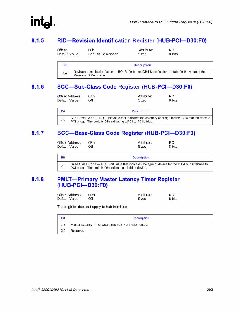
Intel® 82801DBM ICH4-M Datasheet 293
Hub Interface to PCI Bridge Registers (D30:F0)
8.1.5 RID�Revision Identification Register (HUB-PCI�D30:F0)Offset: 08h Attribute: RODefault Value: See Bit Description Size: 8 Bits
8.1.6 SCC�Sub-Class Code Register (HUB-PCI�D30:F0)Offset Address: 0Ah Attribute: RODefault Value: 04h Size: 8 bits
8.1.7 BCC�Base-Class Code Register (HUB-PCI�D30:F0)Offset Address: 0Bh Attribute: RODefault Value: 06h Size: 8 bits
8.1.8 PMLT�Primary Master Latency Timer Register (HUB-PCI�D30:F0)Offset Address: 0Dh Attribute: RODefault Value: 00h Size: 8 bits
This register does not apply to hub interface.
Bit Description
7:0 Revision Identification Value � RO. Refer to the ICH4 Specification Update for the value of the Revision ID Register.e
Bit Description
7:0 Sub Class Code � RO. 8-bit value that indicates the category of bridge for the ICH4 hub interface to PCI bridge. The code is 04h indicating a PCI-to-PCI bridge.
Bit Description
7:0 Base Class Code � RO. 8-bit value that indicates the type of device for the ICH4 hub interface to PCI bridge. The code is 06h indicating a bridge device.
Bit Description
7:3 Master Latency Timer Count (MLTC). Not implemented.
2:0 Reserved

294 Intel® 82801DBM ICH4-M Datasheet
Hub Interface to PCI Bridge Registers (D30:F0)
8.1.9 HEADTYP�Header Type Register (HUB-PCI�D30:F0)Offset Address: 0Eh Attribute: RODefault Value: 01h Size: 8 bits
8.1.10 PBUS_NUM�Primary Bus Number Register (HUB-PCI�D30:F0)Offset Address: 18h Attribute: RODefault Value: 00h Size: 8 bits
8.1.11 SBUS_NUM�Secondary Bus Number Register(HUB-PCI�D30:F0)Offset Address: 19h Attribute: R/WDefault Value: 00h Size: 8 bits
8.1.12 SUB_BUS_NUM�Subordinate Bus Number Register (HUB-PCI�D30:F0)Offset Address: 1A Attribute: R/WDefault Value: 00h Size: 8 bits
Bit Description
7 Multi-Function Device � RO. This bit is 0 to indicate a single function device.
6:0 Header Type � RO. 8-bit field identifies the header layout of the configuration space, which is a PCI-to-PCI bridge in this case.
Bit Description
7:0 Primary Bus Number � RO. This field indicates the bus number of the hub interface and is hardwired to 00h.
Bit Description
7:0Secondary Bus Number � R/W. This field indicates the bus number of PCI. Note: when this number is equal to the primary bus number (i.e., bus #0), the ICH4 will run hub interface configuration cycles to this bus number as Type 1 configuration cycles on PCI.
Bit Description
7:0Subordinate Bus Number � R/W. This field specifies the highest PCI bus number below the hub interface to PCI bridge. If a Type 1 configuration cycle from the hub interface does not fall in the Secondary-to-Subordinate Bus ranges of Device 30, the ICH4 will indicate a master abort back to the hub interface.

Intel® 82801DBM ICH4-M Datasheet 295
Hub Interface to PCI Bridge Registers (D30:F0)
8.1.13 SMLT�Secondary Master Latency Timer Register (HUB-PCI�D30:F0)Offset Address: 1Bh Attribute: R/WDefault Value: 00h Size: 8 bits
This Master Latency Timer (MLT) controls the amount of time that the ICH4 will continue to burst data as a master on the PCI bus. When the ICH4 starts the cycle after being granted the bus, the counter is loaded and starts counting down from the assertion of FRAME#. If the internal grant to this device is removed, then the expiration of the MLT counter will result in the deassertion of FRAME#. If the internal grant has not been removed, then the ICH4 can continue to own the bus.
8.1.14 IOBASE�I/O Base Register (HUB-PCI�D30:F0)Offset Address: 1Ch Attribute: R/W, RODefault Value: F0h Size: 8 bits
8.1.15 IOLIM�I/O Limit Register (HUB-PCI�D30:F0)Offset Address: 1Dh Attribute: R/W, RODefault Value: 00h Size: 8 bits
Bit Description
7:3 Master Latency Timer Count (MLTC) � R/W. 5-bit value that indicates the number of PCI clocks, in 8-clock increments, that the ICH4 will remain as master of the bus.
2:0 Reserved
Bit Description
7:4 I/O Address Base Bits [15:12] � R/W. I/O Base bits corresponding to address lines 15:12 for 4-KB alignment. Bits 11:0 are assumed to be padded to 000h.
3:0I/O Addressing Capability � RO. This is hardwired to 0h, indicating that the hub interface to PCI bridge does not support 32-bit I/O addressing. This means that the I/O base & limit upper address registers must be read only.
Bit Description
7:4 I/O Address Limit Bits [15:12] � R/W. I/O Base bits corresponding to address lines 15:12 for 4-KB alignment. Bits 11:0 are assumed to be padded to FFFh.
3:0I/O Addressing Capability � RO. This is hardwired to 0h, indicating that the hub interface-to-PCI bridge does not support 32-bit I/O addressing. This means that the I/O Base and I/O Limit Upper Address registers must be read only.

296 Intel® 82801DBM ICH4-M Datasheet
Hub Interface to PCI Bridge Registers (D30:F0)
8.1.16 SECSTS�Secondary Status Register (HUB-PCI�D30:F0)Offset Address: 1E�1Fh Attribute: R/WCDefault Value: 0280h Size: 16 bits
For the writable bits in this register, writing a 1 will clear the bit. Writing a 0 to the bit will have no effect.
Bit Description
15Detected Parity Error (DPE) � R/WC.0 = This bit is cleared by software writing a 1.1 = ICH4 detected a parity error on the PCI bus.
14Received System Error (SSE) � R/WC.0 = Software clears this bit by writing a 1 to the bit position.1 = SERR# assertion is received on PCI.
13Received Master Abort (RMA) � R/WC.0 = Software clears this bit by writing a 1 to the bit position.1 = Hub interface to PCI cycle is master-aborted on PCI.
12
Received Target Abort (RTA) � R/WC.0 = Software clears this bit by writing a 1 to the bit position.1 = Hub interface to PCI cycle is target-aborted on PCI. For �completion required� cycles from the
hub interface, this event should also set the Signaled Target Abort in the Primary Status Register in this device, and the ICH4 must send the �target abort� status back to the hub interface.
11 Signaled Target Abort (STA) �RO. The ICH4 does not generate target aborts.
10:9DEVSEL# Timing Status (DEV_STS) � RO. 01h = Medium timing.
8
Master Data Parity Error Detected (MDPD) � R/WC.0 = Software clears this bit by writing a 1 to the bit position.1 = The ICH4 sets this bit when all of the following three conditions are met:
� The Parity Error Response Enable bit in the Bridge Control Register (bit 0, offset 3Eh) is set� USB, AC �97 or IDE is a Master � PERR# asserts during a write cycle OR a parity error is detected internally during a read cycle
7 Fast Back to Back Capable (FB2BC) � RO. Hardwired to 1 to indicate that the PCI to hub interface target logic is capable of receiving fast back-to-back cycles.
6 User Definable Features (UDF) � RO. Hardwired to 0.
5 66 MHz Capable (66MHZ_CAP) � RO. Hardwired to 0.
4:0 Reserved

Intel® 82801DBM ICH4-M Datasheet 297
Hub Interface to PCI Bridge Registers (D30:F0)
8.1.17 MEMBASE�Memory Base Register (HUB-PCI�D30:F0)Offset Address: 20�21h Attribute: R/WDefault Value: FFF0h Size: 16 bits
This register defines the base of the hub interface to PCI non-prefetchable memory range. Since the ICH4 will forward all hub interface memory accesses to PCI, the ICH4 will only use this information for determining when not to accept cycles as a target.
This register must be initialized by the configuration software. For the purpose of address decode, address bits A[19:0] are assumed to be 0. Thus, the bottom of the defined memory address range will be aligned to a 1-MB boundary.
8.1.18 MEMLIM�Memory Limit Register (HUB-PCI�D30:F0)Offset Address: 22�23h Attribute: R/WDefault Value: 0000h Size: 16 bits
This register defines the upper limit of the hub interface to PCI non-prefetchable memory range. Since the ICH4 will forward all hub interface memory accesses to PCI, the ICH4 will only use this information for determining when not to accept cycles as a target.
This register must be initialized by the config software. For the purpose of address decode, address bits A[19:0] are assumed to be FFFFFh. Thus, the top of the defined memory address range will be aligned to a 1-MB boundary.
8.1.19 PREF_MEM_BASE�Prefetchable Memory Base Register (HUB-PCI�D30:F0)Offset Address: 24h�25h Attribute: R/WDefault Value: 0000FFF0h Size: 16 bit
Bit Description
15:4 Memory Address Base � R/W. Defines the base of the memory range for PCI. These 12 bits correspond to address bits 31:20.
3:0 Reserved
Bit Description
15:4 Memory Address Limit � R/W. Defines the top of the memory range for PCI. These 12 bits correspond to address bits 31:20.
3:0 Reserved
Bit Description
15:4 Prefetchable Memory Address Base � R/W. Defines the base address of the prefetchable memory address range for PCI. These 12 bits correspond to address bits 31:20.
3:0 Reserved. RO.

298 Intel® 82801DBM ICH4-M Datasheet
Hub Interface to PCI Bridge Registers (D30:F0)
8.1.20 PREF_MEM_MLT�Prefetchable Memory Limit Register (HUB-PCI�D30:F0)Offset Address: 26h�27h Attribute: R/WDefault Value: 00000000h Size: 16 bit
8.1.21 IOBASE_HI�I/O Base Upper 16 Bits Register (HUB-PCI�D30:F0)Offset Address: 30�31h Attribute: RODefault Value: 0000h Size: 16 bits
8.1.22 IOLIM_HI�I/O Limit Upper 16 Bits Register (HUB-PCI�D30:F0)Offset Address: 32�33h Attribute: RODefault Value: 0000h Size: 16 bits
8.1.23 INT_LINE�Interrupt Line Register (HUB-PCI�D30:F0)Offset Address: 3Ch Attribute: RODefault Value: 00h Size: 8 bits
Bit Description
15:4 Prefetchable Memory Address Limit � RW. Defines the limit address of the prefetchable memory address range for PCI. These 12 bits correspond to address bits 31:20.
3:0 Reserved. RO
Bit Description
15:0 I/O Address Base Upper 16 Bits [31:16] � RO. Not supported; hardwired to 0.
Bit Description
15:0 I/O Address Limit Upper 16 Bits [31:16] � RO. Not supported; hardwired to 0.
Bit Description
7:0 Interrupt Line (INT_LN) � RO. Hardwired to 00h. The bridge does not generate interrupts, and interrupts from downstream devices are routed around the bridge.

Intel® 82801DBM ICH4-M Datasheet 299
Hub Interface to PCI Bridge Registers (D30:F0)
8.1.24 BRIDGE_CNT�Bridge Control Register (HUB-PCI�D30:F0)Offset Address: 3E�3Fh Attribute: R/W, R/WC, RODefault Value: 0000h Size: 16 bits
Bit Description
15:12 Reserved
11
Discard Timer SERR# Enable (DTSE) � R/W. Controls the generation of SERR# on the primary interface in response to a timer discard on the secondary interface:0 = Do not generate SERR# on a secondary timer discard1 = Generate SERR# in response to a secondary timer discard.
NOTE: This bit replaces bit 1 of offset 90h, which held this function in ICH3.
10
Discard Timer Status (DTS) � R/WC. 0 = Not Expired. Software clears this bit by writing a 1 to the bit position. 1 = Secondary discard timer expired (there is no discard timer for the primary interface)
NOTE: This bit replaces bit 1 of offset 92h, which had this function in ICH3.
9
Secondary Discard Timer (SDT) � R/W. Sets the maximum number of PCI clock cycles that the ICH4 waits for an initiator on PCI to repeat a delayed transaction request. The counter starts once the delayed transaction completion is at the head of the queue. If the master has not repeated the transaction at least once before the counter expires, the ICH4 discards the transaction from its queue.0 = The PCI master timeout value is between 215 and 216 PCI clocks1 = The PCI master timeout value is between 210 and 211 PCI clocks
8 Primary Discard Timer (PDT) � R/W. This bit is RW for software compatibility only.
7 Fast Back to Back Enable � RO. Hardwired to 0. The PCI logic will not generate fast back-to-back cycles on the PCI bus.
6 Secondary Bus Reset � RO. Hardwired to 0. The ICH4 does not follow the P2P bridge reset scheme; Software-controlled resets are implemented in the PCI-LPC device.
5
Master Abort Mode � R/W. This bit controls the behavior of the ICH4 when a master abort occurs on a transaction that crosses the hub interface-PCI bridge in either direction. The default is 0. 0 = ICH4 behaves in the following manner:
� Hub Interface Completion-Required requests to PCI: when these master abort on PCI, the ICH4 returns a master abort status. For reads, FFFFh is returned for each DWORD.
� Hub Interface Posted Writes to PCI: when these master abort on PCI, the ICH4 discards the data.� PCI Reads to Hub Interface: when these master abort on Hub Interface, the ICH4 returns the
data provided with the Hub Interface master abort packet to the PCI requestor.� PCI writes to Hub Interface: the ICH4 has no idea when these �master-abort.�
1 = ICH4 treats the master abort as an error:� Hub Interface Completion-Required requests to PCI: when these master abort on PCI, the ICH4
returns a target abort status. For reads, FFFFh is returned for each DWORD.� Hub Interface Posted Writes to PCI: when these master abort on PCI, the ICH4 discards the data
and sets the Primary Signaled SERR# bit (if the corresponding SERR_EN bit is set).� PCI Reads to Hub Interface: when these master abort on Hub Interface, the ICH4 terminates the
cycle with a target abort and flushes the remainder of the prefetched data.� PCI writes to Hub Interface: the ICH4 has no idea when these �master-abort.�
4VGA 16-Bit Decode. This bit does not have any functionality relative to address decodes because the ICH4 will forward the cycles to PCI, independent of the decode. Writes of 1 have no impact other than to force the bit to 1. Writes of 0 have no impact other than to force the bit to 0. Reads to this bit will return the previously written value (or 0 if no writes since reset).

300 Intel® 82801DBM ICH4-M Datasheet
Hub Interface to PCI Bridge Registers (D30:F0)
8.1.25 HI1_CMD�Hub Interface 1 Command Control Register (HUB-PCI�D30:F0)Offset Address: 40�43h Attribute: R/W, RODefault Value: 00202802h Size: 32 bits
3
VGA Enable � R/W.0 = No VGA device on PCI.1 = Indicates that the VGA device is on PCI. Therefore, the PCI to hub interface decoder will not
accept memory cycles in the range A0000h�BFFFFh. Note that the ICH4 will never take I/O cycles in the VGA range from PCI.
2ISA Enable � R/W. The ICH4 ignores this bit. However, this bit is read/write for software compatibility. Since the ICH4 forwards all I/O cycles that are not in the USB, AC �97, or IDE ranges to PCI, this bit would have no effect.
1
SERR# Enable � R/W. 0 = Disable1 = If this bit is set AND bit 8 in CMD register (D30:F0 Offset 04h) is also set, the ICH4 will set the
SSE bit in PD_STS register (D30:F0, offset 06h, bit 14) and also generate an NMI (or SMI# if NMI routed to SMI) when the SERR# signal is asserted.
0Parity Error Response Enable � R/W.0 = Disable1 = Enable the hub interface to PCI bridge for parity error detection and reporting on the PCI bus.
Bit Description
Bit Description
31:24 Reserved
23:21Hub ID � RO. This field identifies the Hub Interface ID number for the Intel ICH4. The Intel ICH4 will use this field for sending request packets from the Intel ICH4, and for routing completion packets back from HI1.
20 Reserved
19:16HI Timeslice � R/W. This field sets the HI arbiter time-slice value with 4 base-clock granularity. A value of 0h means that the time-slice is immediately expired and that the ICH4 will allow the other master�s request to be serviced after every message.
15:14 HI_Width � RO. This field is hardwired to 00b, indicating that the HI interface is 8 bits wide.
13 HI_Rate_Valid � RO. Hardwired to 1.
12:10
HI_Rate � RO. Encoded value representing the clock-to-transfer rate of the HI1 interface:010 = 1:4 The value is loaded at reset by sampling the capability of the device connected to the HI1 port. The value for this field is fixed for 4x mode only.
9:4 Reserved.
3:1Max Data (MAXD) � RO. Hardwired to 001b. This field specifies the maximum amount of data that the ICH4 is allowed to burst in one packet on the hub interface. The ICH4 will always do 64-byte bursts.
0 Reserved

Intel® 82801DBM ICH4-M Datasheet 301
Hub Interface to PCI Bridge Registers (D30:F0)
8.1.26 DEVICE_HIDE�Secondary PCI Device Hiding Register (HUB-PCI�D30:F0)Offset Address: 44�45h Attribute: R/WDefault Value: 00h Size: 16 bitsPower Well: 00h
This register allows software to �hide� PCI devices (0 through 5) in terms of configuration space. Specifically, when PCI devices (0�5) are hidden, the configuration space is not accessible because the PCI IDSEL pin does not assert. The ICH4 supports the hiding of 6 external devices (0 through 5), which matches the number of PCI request/grant pairs, and the ability to hide the integrated LAN device by masking out the configuration space decode of LAN controller. Writing a 1 to this bit will not restrict the configuration cycle to the PCI bus. This differs from bits 0 through 5 in which the configuration cycle is restricted.
Hiding a PCI device can be useful for debugging, bug work-arounds, and system management support. Devices should only be hidden during initialization before any configuration cycles are run. This guarantees that the device is not in a semi-enable state.
Bit Description
15:9 Reserved
8HIDE_DEV8�R/W. Same as bit 0 of this register, except for device 8 (AD[24]), which is hardwired to the integrated LAN device. This bit will not change the way the configuration cycle appears on PCI bus
7:6 Reserved
5 HIDE_DEV5�R/W. Same as bit 0 of this register, except for device 5 (AD[21]).
4 HIDE_DEV4�R/W. Same as bit 0 of this register, except for device 4 (AD[20]).
3 HIDE_DEV3�R/W. Same as bit 0 of this register, except for device 3 (AD[19]).
2 HIDE_DEV2�R/W. Same as bit 0 of this register, except for device 2 (AD[18]).
1 HIDE_DEV1�R/W. Same as bit 0 of this register, except for device 1 (AD[17]).
0
HIDE_DEV0�R/W. 0 = PCI configuration cycles for this slot are not affected.1 = Device 0 is hidden on the PCI bus. This is done by masking the IDSEL (keeping it low) for
configuration cycles to that device. Since the device will not see its IDSEL go active, it will not respond to PCI configuration cycles and the processor will think the device is not present. AD[16] is used as IDSEL for device 0.

302 Intel® 82801DBM ICH4-M Datasheet
Hub Interface to PCI Bridge Registers (D30:F0)
8.1.27 CNF�ICH4 Configuration Register (HUB-PCI�D30:F0)Offset Address: 50�51h Attribute: R/WDefault Value: 1400h Size: 16 bits
8.1.28 MTT�Multi-Transaction Timer Register (HUB-PCI�D30:F0)Offset Address: 70h Attribute: R/WDefault Value: 20h Size: 8 bits
MTT is an 8-bit register that controls the amount of time that the ICH4�s arbiter allows a PCI initiator to perform multiple back-to-back transactions on the PCI bus. The ICH4�s MTT mechanism is used to guarantee a fair share of the Primary PCI bandwidth to an initiator that performs multiple back-to-back transactions to fragmented memory ranges (and as a consequence it can not use long burst transfers).
The number of clocks programmed in the MTT represents the guaranteed time slice (measured in PCI clocks) allotted to the current agent, after which the arbiter will grant another agent that is requesting the bus. The MTT value must be programmed with 8 clock granularity in the same manner as MLT. For example, if the MTT is programmed to 18h, then the selected value corresponds to the time period of 24 PCI clocks.The default value of MTT is 20h (32 PCI clocks).
Note: Programming the MTT to a value of 00h disables this function, which could cause starvation problems for some PCI master devices. Programming of the MTT to anything less than 16 clocks will not allow the Grant-to-FRAME# latency to be 16 clocks. The MTT timer will timeout before the Grant-to-FRAME# trigger causing a re-arbitration. MTT timer must be set to greater than 16 clocks.
Bit Description
15:14 Reserved
13Prefetch Flush Enable - R/W. When set, this bit causes CPU to PCI logic to only deliver �Demand� data for a delayed transaction if a CPU to PCI write has occurred since the delayed transaction was initiated. This bit must be set by system BIOS.
12:10 Reserved
9High Priority PCI Enable (HP_PCI_EN) � R/W. 0 = All PCI REQ#/GNT pairs have the same arbitration priority.1 = Enables a mode where the REQ[0]#/GNT[0]# signal pair has a higher arbitration priority.
8Hole Enable (15 MB�16 MB) � R/W. 0 = Disable1 = Enables the 15 MB to 16 MB hole in main memory.
7:2 Reserved
1
12-Clock Retry Enable � R/W. System BIOS must set this bit for PCI compliance.0 = If this bit is not set, the ICH4 will insert as many wait states as needed to complete the PCI to
memory cycle.0 = The ICH4 will retry a PCI to memory cycle (reads or writes) if the ICH4 is not able to complete
the transfer in 12 PCI clocks.
0 Reserved
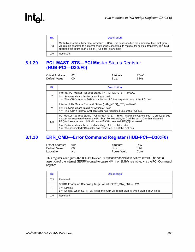
Intel® 82801DBM ICH4-M Datasheet 303
Hub Interface to PCI Bridge Registers (D30:F0)
8.1.29 PCI_MAST_STS�PCI Master Status Register (HUB-PCI�D30:F0)Offset Address: 82h Attribute: R/WCDefault Value: 00h Size: 8 bits
8.1.30 ERR_CMD�Error Command Register (HUB-PCI�D30:F0)Offset Address: 90h Attribute: R/WDefault Value: 00h Size: 8 bitLockable: No Power Well: Core
This register configures the ICH4�s Device 30 responses to various system errors. The actual assertion of the internal SERR# (routed to cause NMI# or SMI#) is enabled via the PCI Command register.
Bit Description
7:3Multi-Transaction Timer Count Value � R/W. This field specifies the amount of time that grant will remain asserted to a master continuously asserting its request for multiple transfers. This field specifies the count in an 8-clock (PCI clock) granularity.
2:0 Reserved
Bit Description
7Internal PCI Master Request Status (INT_MREQ_STS) � R/WC.0 = Software clears this bit by writing a 1 to it.1 = The ICH4�s internal DMA controller or LPC has requested use of the PCI bus.
6Internal LAN Master Request Status (LAN_MREQ_STS) � R/WC.0 = Software clears this bit by writing a 1 to it.1 = The ICH4�s internal LAN controller has requested use of the PCI bus.
5:0
PCI Master Request Status (PCI_MREQ_STS) � R/WC. Allows software to see if a particular bus master has requested use of the PCI bus. For example, bit 0 will be set if ICH4 has detected REQ[0]# asserted and bit 5 will be set if ICH4 detected REQ[5]# asserted. 0 = Software clears these bits by writing a 1 to the bit position.1 = The associated PCI master has requested use of the PCI bus.
Bit Description
7:3 Reserved
2SERR# Enable on Receiving Target Abort (SERR_RTA_EN) � R/W.0 = Disable.1 = Enable. When SERR_EN is set, the ICH4 will report SERR# when SERR_RTA is set.
1:0 Reserved

304 Intel® 82801DBM ICH4-M Datasheet
Hub Interface to PCI Bridge Registers (D30:F0)
8.1.31 ERR_STS�Error Status Register (HUB-PCI�D30:F0)Offset Address: 92h Attribute: R/WDefault Value: 00h Size: 8 bitLockable: No Power Well: Core
This register records the cause of system errors in Device 30. The actual assertion of SERR# is enabled via the PCI Command register.
Bit Description
7:3 Reserved
2
SERR# Due to Received Target Abort (SERR_RTA) � R/W.0 = Software clears this bit by writing a 1 to it.1 = The ICH4 sets this bit when the ICH4 receives a target abort. If SERR_EN, the ICH4 will also
generate an SERR# when SERR_RTA is set.
1:0 Reserved
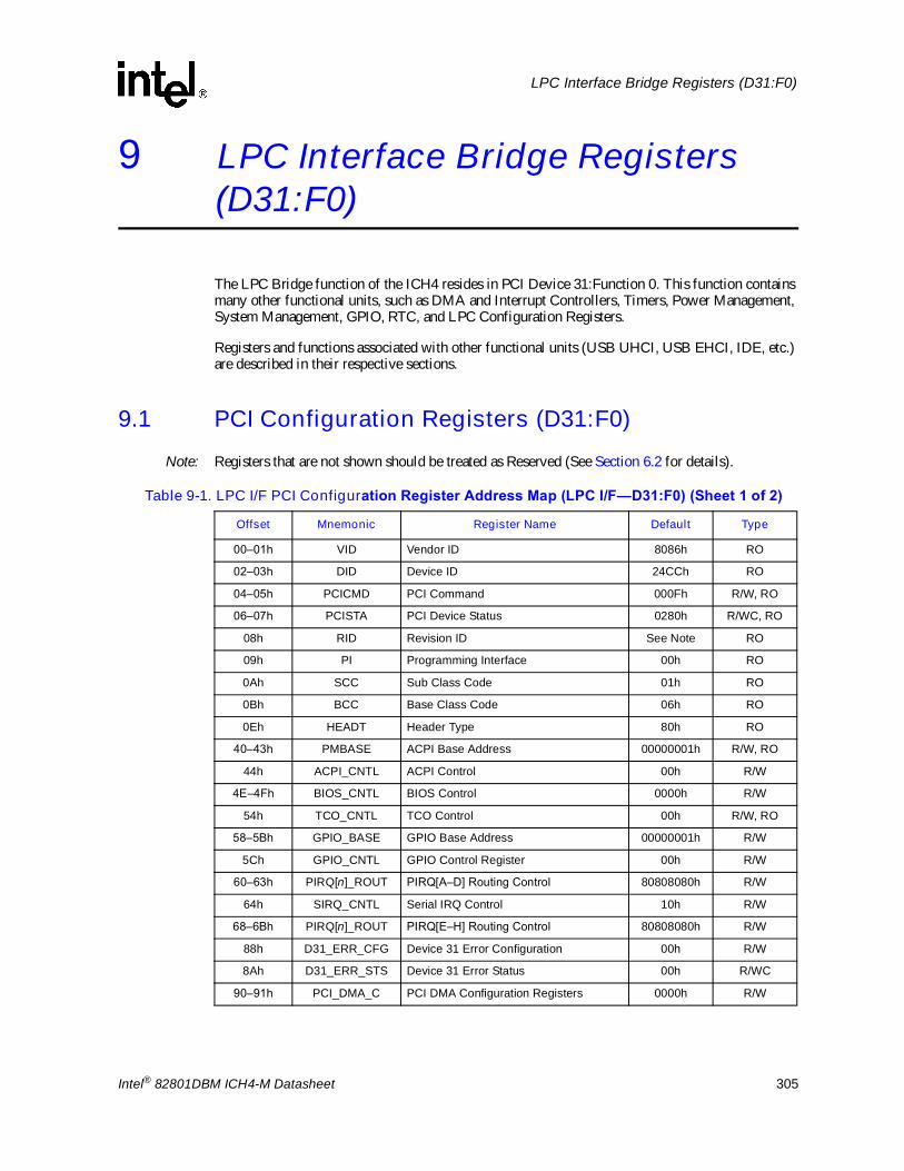
Intel® 82801DBM ICH4-M Datasheet 305
LPC Interface Bridge Registers (D31:F0)
9 LPC Interface Bridge Registers (D31:F0)
The LPC Bridge function of the ICH4 resides in PCI Device 31:Function 0. This function contains many other functional units, such as DMA and Interrupt Controllers, Timers, Power Management, System Management, GPIO, RTC, and LPC Configuration Registers.
Registers and functions associated with other functional units (USB UHCI, USB EHCI, IDE, etc.) are described in their respective sections.
9.1 PCI Configuration Registers (D31:F0)Note: Registers that are not shown should be treated as Reserved (See Section 6.2 for details).
.
Table 9-1. LPC I/F PCI Configuration Register Address Map (LPC I/F�D31:F0) (Sheet 1 of 2)
Offset Mnemonic Register Name Default Type
00�01h VID Vendor ID 8086h RO
02�03h DID Device ID 24CCh RO
04�05h PCICMD PCI Command 000Fh R/W, RO
06�07h PCISTA PCI Device Status 0280h R/WC, RO
08h RID Revision ID See Note RO
09h PI Programming Interface 00h RO
0Ah SCC Sub Class Code 01h RO
0Bh BCC Base Class Code 06h RO
0Eh HEADT Header Type 80h RO
40�43h PMBASE ACPI Base Address 00000001h R/W, RO
44h ACPI_CNTL ACPI Control 00h R/W
4E�4Fh BIOS_CNTL BIOS Control 0000h R/W
54h TCO_CNTL TCO Control 00h R/W, RO
58�5Bh GPIO_BASE GPIO Base Address 00000001h R/W
5Ch GPIO_CNTL GPIO Control Register 00h R/W
60�63h PIRQ[n]_ROUT PIRQ[A�D] Routing Control 80808080h R/W
64h SIRQ_CNTL Serial IRQ Control 10h R/W
68�6Bh PIRQ[n]_ROUT PIRQ[E�H] Routing Control 80808080h R/W
88h D31_ERR_CFG Device 31 Error Configuration 00h R/W
8Ah D31_ERR_STS Device 31 Error Status 00h R/WC
90�91h PCI_DMA_C PCI DMA Configuration Registers 0000h R/W

306 Intel® 82801DBM ICH4-M Datasheet
LPC Interface Bridge Registers (D31:F0)
NOTE: Refer to the ICH4 Specification Update for the value of the Revision ID Register.
9.1.1 VID�Vendor ID Register (LPC I/F�D31:F0)Offset Address: 00�01h Attribute: RODefault Value: 8086h Size: 16 bitLockable: No Power Well: Core
9.1.2 DID�Device ID Register (LPC I/F�D31:F0)Offset Address: 02�03h Attribute: RODefault Value: 24CCh Size: 16 bitLockable: No Power Well: Core
A0�CFh Power Management Registers(See Section 9.8.1)
D0�D3h GEN_CNTL General Control 00000000h R/W
D4h GEN_STA General Status 0Xh R/W-Special, RO
D5h BACK_CNTL Backed Up Control Depends on Strap R/W
D8h RTC_CONF Real Time Clock Configuration 00h R/W
E0h COM_DEC LPC I/F COM Port Decode Ranges 00h R/W
E1h LPCFDD_DEC LPC I/F FDD & LPT Decode Ranges 00h R/W
E2h SND_DEC LPC I/F Sound Decode Ranges 00h R/W
E3h FWH_DEC_EN1 FWH Decode Enable 1 FFh R/W
E4�E5h GEN1_DEC LPC I/F General 1 Decode Range 0000h R/W
E6�E7h LPC_EN LPC I/F Enables 00h R/W
E8�EBh FWH_SEL1 FWH Select 1 00112233h R/W
EC�EDh GEN2_DEC LPC I/F General 2 Decode Range 0000h R/W
EE�EFh FWH_SEL2 FWH Select 2 5678h R/W
F0h FWH_DEC_EN2 FWH Decode Enable 2 0Fh R/W
F2h FUNC_DIS Function Disable Register 00h R/W
Table 9-1. LPC I/F PCI Configuration Register Address Map (LPC I/F�D31:F0) (Sheet 2 of 2)
Offset Mnemonic Register Name Default Type
Bit Description
15:0 Vendor Identification Value � RO. This is a 16-bit value assigned to Intel. Intel VID = 8086h
Bit Description
15:0 Device Identification Value � RO. This is a 16-bit value assigned to the ICH4 LPC Bridge.

Intel® 82801DBM ICH4-M Datasheet 307
LPC Interface Bridge Registers (D31:F0)
9.1.3 PCICMD�PCI COMMAND Register (LPC I/F�D31:F0)Offset Address: 04�05h Attribute: R/W, RODefault Value: 000Fh Size: 16 bitLockable: No Power Well: Core
Bit Description
15:10 Reserved
9 Fast Back to Back Enable (FBE) � RO. Hardwired to 0.
8SERR# Enable (SERR_EN) � R/W. 0 = Disable.1 = Enable. Allow SERR# to be generated.
7 Wait Cycle Control (WCC) � RO. Hardwired to 0.
6Parity Error Response (PER) � R/W. 0 = No action is taken when detecting a parity error.1 = The ICH will take normal action when a parity error is detected.
5 VGA Palette Snoop (VPS) � RO. Hardwired to 0
4 Postable Memory Write Enable (PMWE) � RO. Hardwired to 0
3 Special Cycle Enable (SCE) � Hardwired to 1.
2 Bus Master Enable (BME) � RO. Hardwired to 1 to indicate that bus mastering cannot be disabled for function 0 (DMA/ISA Master)
1 Memory Space Enable (MSE) � RO. Hardwired to 1 to indicate that memory space cannot be disabled for Function 0 (LPC I/F)
0 I/O Space Enable (IOSE) � RO. Hardwired to 1 to indicate that the I/O space cannot be disabled for function 0 (LPC I/F)

308 Intel® 82801DBM ICH4-M Datasheet
LPC Interface Bridge Registers (D31:F0)
9.1.4 PCISTA�PCI Device Status (LPC I/F�D31:F0)Offset Address: 06�07h Attribute: R/WC, RODefault Value: 0280h Size: 16 bitLockable: No Power Well: Core
9.1.5 REVID�Revision ID Register (LPC I/F�D31:F0)Offset Address: 08h Attribute: RODefault Value: See Bit Description Size: 8 bits
Bit Description
15Detected Parity Error (DPE) � R/WC.0 = This bit is cleared by software writing a 1 to the bit position.1 = PERR# signal goes active. Set even if the PER bit is 0.
14
Signaled System Error (SSE) � R/WC.0 = This bit is cleared by software writing a 1 to the bit position.1 = Set by the ICH4 if the SERR_EN bit is set and the ICH4 generates an SERR# on function 0. The
ERR_STS register can be read to determine the cause of the SERR#. The SERR# can be routed to cause SMI#, NMI, or interrupt.
13Master Abort Status (RMA) � R/WC. 0 = This bit is cleared by software writing a 1 to the bit position.1 = ICH4 generated a master abort on PCI due to LPC I/F master or DMA cycles.
12Received Target Abort (RTA) � R/WC. 0 = This bit is cleared by software writing a 1 to the bit position.1 = ICH4 received a target abort during LPC I/F master or DMA cycles to PCI.
11
Signaled Target Abort (STA) � R/WC. 0 = This bit is cleared by software writing a 1 to the bit position.1 = ICH4 generated a target abort condition on PCI cycles claimed by the ICH4 for ICH4 internal
registers or for going to LPC I/F.
10:9DEVSEL# Timing Status (DEV_STS) � RO. 01 = Medium Timing.
8
Data Parity Error Detected (DPED) � R/WC.0 = This bit is cleared by software writing a 1 to the bit position.1 = Set when all three of the following conditions are true:
- The ICH4 is the initiator of the cycle, - The ICH4 asserted PERR# (for reads) or observed PERR# (for writes), and- The PER bit is set.
7 Fast Back to Back Capable (FB2BC) � RO. Hardwired to 1. Indicates ICH4 as a target can accept fast back-to-back transactions.
6 User Definable Features (UDF) � RO. Hardwired to 0
5 66 MHz Capable (66MHZ_CAP) � RO. Hardwired to 0
4:0 Reserved
Bit Description
7:0 Revision Identification Value � RO. Refer to the ICH4 Specification Update for the value of the Revision ID Register.

Intel® 82801DBM ICH4-M Datasheet 309
LPC Interface Bridge Registers (D31:F0)
9.1.6 PI�Programming Interface (LPC I/F�D31:F0)Offset Address: 09h Attribute: RODefault Value: 00h Size: 8 bits
9.1.7 SCC�Sub-Class Code Register (LPC I/F�D31:F0)Offset Address: 0Ah Attribute: RODefault Value: 01h Size: 8 bits
9.1.8 BCC�Base-Class Code Register (LPC I/F�D31:F0)Offset Address: 0Bh Attribute: RODefault Value: 06h Size: 8 bits
9.1.9 HEADTYP�Header Type Register (LPC I/F�D31:F0)Offset Address: 0Eh Attribute: RODefault Value: 80h Size: 8 bits
Bit Description
7:0 Programming Interface Value � RO.
Bit Description
7:0 Sub Class Code � RO. This 8-bit value indicates the category of bridge for the LPC PCI bridge.
Bit Description
7:0 Base Class Code � RO. This 8-bit value indicates the type of device for the LPC bridge. The code is 06h indicating a bridge device.
Bit Description
7 Multi-Function Device � RO. This bit is 1 to indicate a multi-function device.
6:0 Header Type � RO. 7-bit field identifies the header layout of the configuration space.

310 Intel® 82801DBM ICH4-M Datasheet
LPC Interface Bridge Registers (D31:F0)
9.1.10 PMBASE�ACPI Base Address (LPC I/F�D31:F0)Offset Address: 40�43h Attribute: R/W, RODefault Value: 00000001h Size: 32 bitLockable: No Usage: ACPI, Legacy
Power Well: Core
Sets base address for ACPI I/O registers, GPIO registers and TCO I/O registers. Can be mapped anywhere in the 64K I/O space on 128-byte boundaries.
9.1.11 ACPI_CNTL�ACPI Control (LPC I/F � D31:F0)Offset Address: 44h Attribute: R/WDefault Value: 00h Size: 8 bitLockable: No Usage: ACPI, Legacy
Power Well: Core
Bit Description
31:16 Reserved
15:7 Base Address � R/W. Provides 128 bytes of I/O space for ACPI, GPIO, and TCO logic. This is placed on a 128-byte boundary.
6:1 Reserved
0 Resource Indicator � RO. Tied to 1 to indicate I/O space.
Bit Description
7:5 Reserved
4
ACPI Enable (ACPI_EN) � R/W.0 = Disable.1 = Decode of the I/O range pointed to by the ACPI Base register is enabled, and the ACPI power
management function is enabled. Note that the APM power management ranges (B2/B3h) are always enabled and are not affected by this bit.
3 Reserved
2:0
SCI IRQ Select (SCI_IRQ_SEL) � R/W. This field specifies on which IRQ the SCI will internally appear. If not using the APIC, the SCI must be routed to IRQ9-11, and that interrupt is not sharable with the SERIRQ stream, but is shareable with other PCI interrupts. If using the APIC, the SCI can also be mapped to IRQ20-23, and can be shared with other interrupts.000 = IRQ9001 = IRQ10010 = IRQ11011 = Reserved100 = IRQ20 (Only available if APIC enabled)101 = IRQ21 (Only available if APIC enabled)110 = IRQ22 (Only available if APIC enabled)111 = IRQ23 (Only available if APIC enabled)
NOTE: When the TCO interrupt is mapped to APIC interrupts 9, 10 or 11, the signal is in fact active high. When the TCO interrupt is mapped to IRQ 20, 21, 22, or 23 the signal is active low and can be shared with PCI interrupts that may be mapped to those same signals (IRQs).

Intel® 82801DBM ICH4-M Datasheet 311
LPC Interface Bridge Registers (D31:F0)
9.1.12 BIOS_CNTL�BIOS Control Register (LPC I/F�D31:F0) Offset Address: 4E�4Fh Attribute: R/WDefault Value: 0000h Size: 16 bitLockable: No Power Well: Core
9.1.13 TCO_CNTL � TCO Control (LPC I/F � D31:F0)Offset Address: 54h Attribute: R/WDefault Value: 00h Size: 8 bitLockable: No Power Well: Core
Bit Description
15:2 Reserved
1
BIOS Lock Enable (BLE) � R/W. 0 = Setting the BIOSWE will not cause Sums. Once set, this bit can only be cleared by a
PCIRST#.1 = Enables setting the BIOSWE bit to cause Sums.
0
BIOS Write Enable (BIOSWE) � R/W. 0 = Only read cycles result in FWH I/F cycles. 1 = Access to the BIOS space is enabled for both read and write cycles. When this bit is written
from a 0 to a 1 and BIOS lock Enable (BLE) is also set, an SMI# is generated. This ensures that only SMI code can update BIOS.
Bits Description
7:4 Reserved
3TCO Interrupt Enable (TCO_INT_EN) � R/W. This bit enables/disables the TCO interrupt.0 = Disables TCO interrupt. 1 = Enables TCO Interrupt, as selected by the TCO_INT_SEL field.
2:0
TCO Interrupt Select (TCO_INT_SEL) � R/W. This field specifies on which IRQ the TCO will internally appear. If not using the APIC, the TCO interrupt must be routed to IRQ9:11, and that interrupt is not sharable with the SERIRQ stream, but is shareable with other PCI interrupts. If using the APIC, the TCO interrupt can also be mapped to IRQ20:23, and can be shared with other interrupt. Note that if the TCOSCI_EN bit is set (bit 6 of the GPEO_EN register), then the TCO interrupt will be sent to the same interrupt as the SCI, and the TCO_INT_SEL bits will have no meaning. When the TCO interrupt is mapped to APIC interrupts 9, 10 or 11, the signal is active high. When the TCO interrupt is mapped to IRQ 20, 21, 22, or 23, the signal is active low and can be shared with PCI interrupts that may be mapped to those same signals (IRQs).000 = IRQ9001 = IRQ10010 = IRQ11011 = Reserved100 = IRQ20 (Only available if APIC enabled)101 = IRQ21 (Only available if APIC enabled)110 = IRQ22 (Only available if APIC enabled)111 = IRQ23 (Only available if APIC enabled)
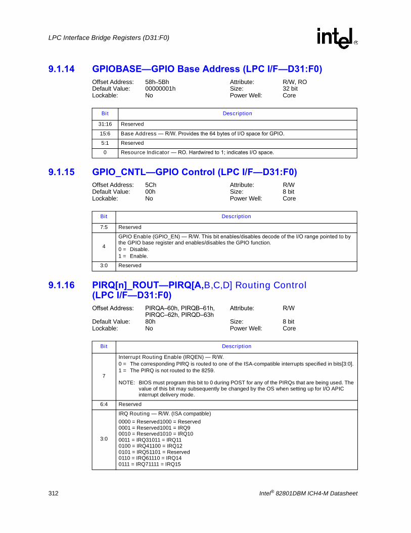
312 Intel® 82801DBM ICH4-M Datasheet
LPC Interface Bridge Registers (D31:F0)
9.1.14 GPIOBASE�GPIO Base Address (LPC I/F�D31:F0)Offset Address: 58h�5Bh Attribute: R/W, RODefault Value: 00000001h Size: 32 bitLockable: No Power Well: Core
9.1.15 GPIO_CNTL�GPIO Control (LPC I/F�D31:F0)Offset Address: 5Ch Attribute: R/WDefault Value: 00h Size: 8 bitLockable: No Power Well: Core
9.1.16 PIRQ[n]_ROUT�PIRQ[A,B,C,D] Routing Control (LPC I/F�D31:F0)Offset Address: PIRQA�60h, PIRQB�61h, Attribute: R/W
PIRQC�62h, PIRQD�63hDefault Value: 80h Size: 8 bitLockable: No Power Well: Core
Bit Description
31:16 Reserved
15:6 Base Address � R/W. Provides the 64 bytes of I/O space for GPIO.
5:1 Reserved
0 Resource Indicator � RO. Hardwired to 1; indicates I/O space.
Bit Description
7:5 Reserved
4
GPIO Enable (GPIO_EN) � R/W. This bit enables/disables decode of the I/O range pointed to by the GPIO base register and enables/disables the GPIO function.0 = Disable.1 = Enable.
3:0 Reserved
Bit Description
7
Interrupt Routing Enable (IRQEN) � R/W. 0 = The corresponding PIRQ is routed to one of the ISA-compatible interrupts specified in bits[3:0]. 1 = The PIRQ is not routed to the 8259.
NOTE: BIOS must program this bit to 0 during POST for any of the PIRQs that are being used. The value of this bit may subsequently be changed by the OS when setting up for I/O APIC interrupt delivery mode.
6:4 Reserved
3:0
IRQ Routing � R/W. (ISA compatible)0000 = Reserved1000 = Reserved0001 = Reserved1001 = IRQ90010 = Reserved1010 = IRQ100011 = IRQ31011 = IRQ110100 = IRQ41100 = IRQ120101 = IRQ51101 = Reserved0110 = IRQ61110 = IRQ140111 = IRQ71111 = IRQ15
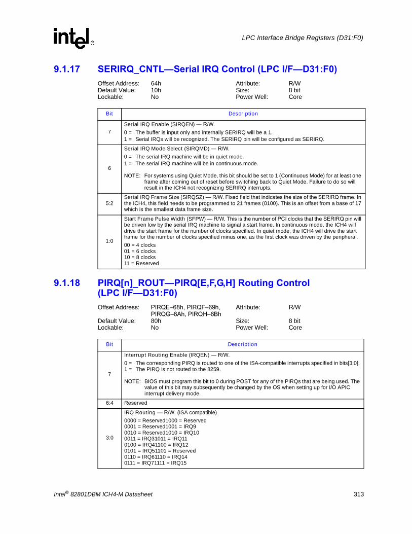
Intel® 82801DBM ICH4-M Datasheet 313
LPC Interface Bridge Registers (D31:F0)
9.1.17 SERIRQ_CNTL�Serial IRQ Control (LPC I/F�D31:F0)Offset Address: 64h Attribute: R/WDefault Value: 10h Size: 8 bitLockable: No Power Well: Core
9.1.18 PIRQ[n]_ROUT�PIRQ[E,F,G,H] Routing Control (LPC I/F�D31:F0)Offset Address: PIRQE�68h, PIRQF�69h, Attribute: R/W
PIRQG�6Ah, PIRQH�6BhDefault Value: 80h Size: 8 bitLockable: No Power Well: Core
Bit Description
7Serial IRQ Enable (SIRQEN) � R/W.0 = The buffer is input only and internally SERIRQ will be a 1.1 = Serial IRQs will be recognized. The SERIRQ pin will be configured as SERIRQ.
6
Serial IRQ Mode Select (SIRQMD) � R/W.0 = The serial IRQ machine will be in quiet mode. 1 = The serial IRQ machine will be in continuous mode.
NOTE: For systems using Quiet Mode, this bit should be set to 1 (Continuous Mode) for at least one frame after coming out of reset before switching back to Quiet Mode. Failure to do so will result in the ICH4 not recognizing SERIRQ interrupts.
5:2Serial IRQ Frame Size (SIRQSZ) � R/W. Fixed field that indicates the size of the SERIRQ frame. In the ICH4, this field needs to be programmed to 21 frames (0100). This is an offset from a base of 17 which is the smallest data frame size.
1:0
Start Frame Pulse Width (SFPW) � R/W. This is the number of PCI clocks that the SERIRQ pin will be driven low by the serial IRQ machine to signal a start frame. In continuous mode, the ICH4 will drive the start frame for the number of clocks specified. In quiet mode, the ICH4 will drive the start frame for the number of clocks specified minus one, as the first clock was driven by the peripheral.00 = 4 clocks01 = 6 clocks10 = 8 clocks11 = Reserved
Bit Description
7
Interrupt Routing Enable (IRQEN) � R/W. 0 = The corresponding PIRQ is routed to one of the ISA-compatible interrupts specified in bits[3:0]. 1 = The PIRQ is not routed to the 8259.
NOTE: BIOS must program this bit to 0 during POST for any of the PIRQs that are being used. The value of this bit may subsequently be changed by the OS when setting up for I/O APIC interrupt delivery mode.
6:4 Reserved
3:0
IRQ Routing � R/W. (ISA compatible)0000 = Reserved1000 = Reserved0001 = Reserved1001 = IRQ90010 = Reserved1010 = IRQ100011 = IRQ31011 = IRQ110100 = IRQ41100 = IRQ120101 = IRQ51101 = Reserved0110 = IRQ61110 = IRQ140111 = IRQ71111 = IRQ15

314 Intel® 82801DBM ICH4-M Datasheet
LPC Interface Bridge Registers (D31:F0)
9.1.19 D31_ERR_CFG�Device 31 Error Configuration Register (LPC I/F�D31:F0)Offset Address: 88h Attribute: R/WDefault Value: 00h Size: 8 bitLockable: No Power Well: Core
This register configures the ICH4�s Device 31 responses to various system errors. The actual assertion of SERR# is enabled via the PCI Command register
.
9.1.20 D31_ERR_STS�Device 31 Error Status Register (LPC I/F�D31:F0)Offset Address: 8Ah Attribute: R/WCDefault Value: 00h Size: 8 bitLockable: No Power Well: Core
This register configures the ICH4�s Device 31 responses to various system errors. The actual assertion of SERR# is enabled via the PCI Command register.
Bit Description
7:3 Reserved
2SERR# on Received Target Abort Enable (SERR_RTA_EN) � R/W.0 = Disable. No SERR# assertion on Received Target Abort.1 = The ICH4 will generate SERR# when SERR_RTA is set if SERR_EN is set.
1SERR# on Delayed Transaction Timeout Enable (SERR_DTT_EN) � R/W.0 = Disable. No SERR# assertion on Delayed Transaction Timeout.1 = The ICH4 will generate SERR# when SERR_DTT bit is set if SERR_EN is set.
0 Reserved
Bit Description
7:3 Reserved
2
SERR# Due to Received Target Abort (SERR_RTA) � R/WC.0 = Software clears this bit by writing a 1 to the bit location.1 = The ICH4 sets this bit when it receives a target abort. If SERR_EN, the ICH4 will also generate
an SERR# when SERR_RTA is set.
1
SERR# Due to Delayed Transaction Timeout (SERR_DTT) � R/WC.0 = Software clears this bit by writing a 1 to the bit location.1 = When a PCI master does not return for the data within 1 ms of the cycle�s completion, the ICH4
clears the delayed transaction and sets this bit. If both SERR_DTT_EN and SERR_EN are set, then ICH4 will also generate an SERR# when SERR_DTT is set.
0 Reserved

Intel® 82801DBM ICH4-M Datasheet 315
LPC Interface Bridge Registers (D31:F0)
9.1.21 PCI_DMA_CFG�PCI DMA Configuration (LPC I/F�D31:F0)Offset Address: 90h�91h Attribute: R/WDefault Value: 0000h Size: 16 bitLockable: No Power Well: Core
Bit Description
15:14
Channel 7 Select � R/W.00 = Reserved 01 = PC/PCI DMA10 = Reserved11 = LPC I/F DMA
13:12 Channel 6 Select � R/W. Same bit decode as for Channel 7
11:10 Channel 5 Select � R/W. Same bit decode as for Channel 7
9:8 Reserved
7:6 Channel 3 Select � R/W. Same bit decode as for Channel 7
5:4 Channel 2 Select � R/W. Same bit decode as for Channel 7
3:2 Channel 1 Select � R/W. Same bit decode as for Channel 7
1:0 Channel 0 Select � R/W. Same bit decode as for Channel 7

316 Intel® 82801DBM ICH4-M Datasheet
LPC Interface Bridge Registers (D31:F0)
9.1.22 GEN_CNTL � General Control Register (LPC I/F � D31:F0)Offset Address: D0h�D3h Attribute: R/WDefault Value: 00000000h Size: 32 bitLockable: No Power Well: Core
Bit Description
31:26 Reserved
25
REQ[5]#/GNT[5]# PC/PCI Protocol Select (PCPCIB_SEL) � R/W.0 = REQ[5]#/GNT[5]# pins function as a standard PCI REQ/GNT signal pair. 1 = PCI REQ[5]#/GNT[5]# signal pair use the PC/PCI protocol as REQ[B]#/GNT[B]. The
corresponding bits in the GPIO_USE_SEL register must also be set to a 0. If the corresponding bits in the GPIO_USE_SEL register are set to a 1, then the signals will be used as a GPI and GPO.
24
Hide ISA Bridge (HIDE_ISA) � R/W. 0 = The ICH4 does not prevent AD22 from asserting during configuration cycles to the PCI-to-ISA
bridge.1 = Software sets this bit to 1 to disable configuration cycle from being claimed by a PCI-to-ISA
bridge. This prevents the OS PCI PnP from getting confused by seeing two ISA bridges. It is required for the ICH4 PCI address line AD22 to connect to the PCI-to-ISA bridge�s IDSEL input. When this bit is set, the ICH4 will not assert AD22 during configuration cycles to the PCI-to-ISA bridge.
23:22 Reserved
21
CPU Break Event Indication Enable (FERR#-MUX-EN) � R/W. 0 = Disable. The ICH4 does not examine the FERR# signal during C2, C3, or C4. (Default)1 = Enables the ICH4 to examine the FERR# signal during a C2, C3, or C4 state as a break event.
(See Section 5.12.5 for details.)
20 Reserved
19:18 SCRATCHPAD. These bits are provided for possible future use.
17:14 Reserved
13
Coprocessor Error Enable (COPR_ERR_EN) � R/W.0 = FERR# will not generate IRQ13 nor IGNNE#.1 = When FERR# is low, ICH4 generates IRQ13 internally and holds it until an I/O write to port F0h.
It will also drive IGNNE# active.
12Keyboard IRQ1 Latch Enable (IRQ1LEN) � R/W.0 = IRQ1 bypasses the latch.1 = The active edge of IRQ1 is latched and held until a port 60h read.
11Mouse IRQ12 Latch Enable (IRQ12LEN) � R/W.0 = IRQ12 bypasses the latch.1 = The active edge of IRQ12 is latched and held until a port 60h read.
10:9 Reserved

Intel® 82801DBM ICH4-M Datasheet 317
LPC Interface Bridge Registers (D31:F0)
8
APIC Enable (APIC_EN) � R/W.0 = Disables internal I/O (x) APIC.1 = Enables the internal I/O (x) APIC and its address decode. The following behavioral rules apply for bits 8 and 7 in this register:
� Rule 1: If bit 8 is 0, the ICH4 does not decode any of the registers associated with the I/O APIC or I/O (x) APIC. The state of bit 7 is �Don�t Care� in this case.
� Rule 2: If bit 8 is 1 and bit 7 is 0, the ICH4 decodes the memory space associated with the I/O APIC, but not the extra registers associated I/O (x) APIC.
� Rule 3: If bit 8 is 1 and bit 7 is 1, the ICH4 decodes the memory space associated with both the I/O APIC and the I/O (x) APIC. This also enables PCI masters to write directly to the register to cause interrupts (PCI Message Interrupt).
NOTE: There is no separate way to disable PCI Message Interrupts if the I/O (x) APIC is enabled. This is not considered necessary.
7
I/O (x) Extension Enable (XAPIC_EN) � R/W.0 = The I/O (x) APIC extensions are not supported.1 = Enables the extra features (beyond standard I/O APIC) associated with the I/O (x) APIC.
NOTE: This bit is only valid if the APIC_EN bit is also set to 1.
6
Alternate Access Mode Enable (ALTACC_EN) � R/W.0 = Alt Access Mode Disabled (default). ALT access mode allows reads to otherwise unreadable
registers and writes otherwise unwritable registers.1 = Alt Access Mode Enable.
5:4 Reserved
3
:Mobile IDE Configuration Lock Down (MICLD)� R/WO. 0 = No lock1 = When set, Bits 7:6 of the Backed up Control Register (Offset D5h)can no longer be written until
a PCI reset occurs. This prevents rogue software from changing the default state of the IDE pins during boot after BIOS configures them. This bit is write once, and is cleared by PCIRST# and when returning from the S3/S4/S5 states.
2DMA Collection Buffer Enable (DCB_EN) � R/W.0 = DCB disabled.1 = Enables DMA Collection Buffer (DCB) for LPC I/F and PC/PCI DMA.
1Delayed Transaction Enable (DTE) � R/W.0 = Delayed transactions disabled.1 = ICH4 enables delayed transactions for internal register, FWH and LPC I/F accesses.
0
Positive Decode Enable (POS_DEC_EN) � R/W.0 = The ICH4 will perform subtractive decode on the PCI bus and forward the cycles to LPC I/F if
not to an internal register or other known target on the LPC I/F. Accesses to internal registers and to known LPC I/F devices will still be positively decoded.
1 = Enables ICH4 to only perform positive decode on the PCI bus.
Bit Description

318 Intel® 82801DBM ICH4-M Datasheet
LPC Interface Bridge Registers (D31:F0)
9.1.23 GEN_STA�General Status Register (LPC I/F�D31:F0)Offset Address: D4h Attribute: RO, R/W-SpecialDefault Value: 0Xh Size: 8 bitLockable: No Power Well: Core
Bit Description
7:3 Reserved
2
SAFE_MODE � RO.0 = ICH4 sampled AC_SDOUT low on the rising edge of PWROK.1 = ICH4 sampled AC_SDOUT high on the rising edge of PWROK. ICH4 will force
FREQ_STRAP[3:0] bits to all 1s (safe mode multiplier).
1
NO_REBOOT � R/W-Special.0 = Normal TCO Timer reboot functionality (reboot after 2nd TCO timeout). This bit cannot be set to
0 by software if the strap is set to No Reboot.1 = ICH4 will disable the TCO Timer system reboot feature. This bit is set either by hardware when
SPKR is sampled high on the rising edge of PWROK, or by software writing a 1 to the bit.
0 Reserved
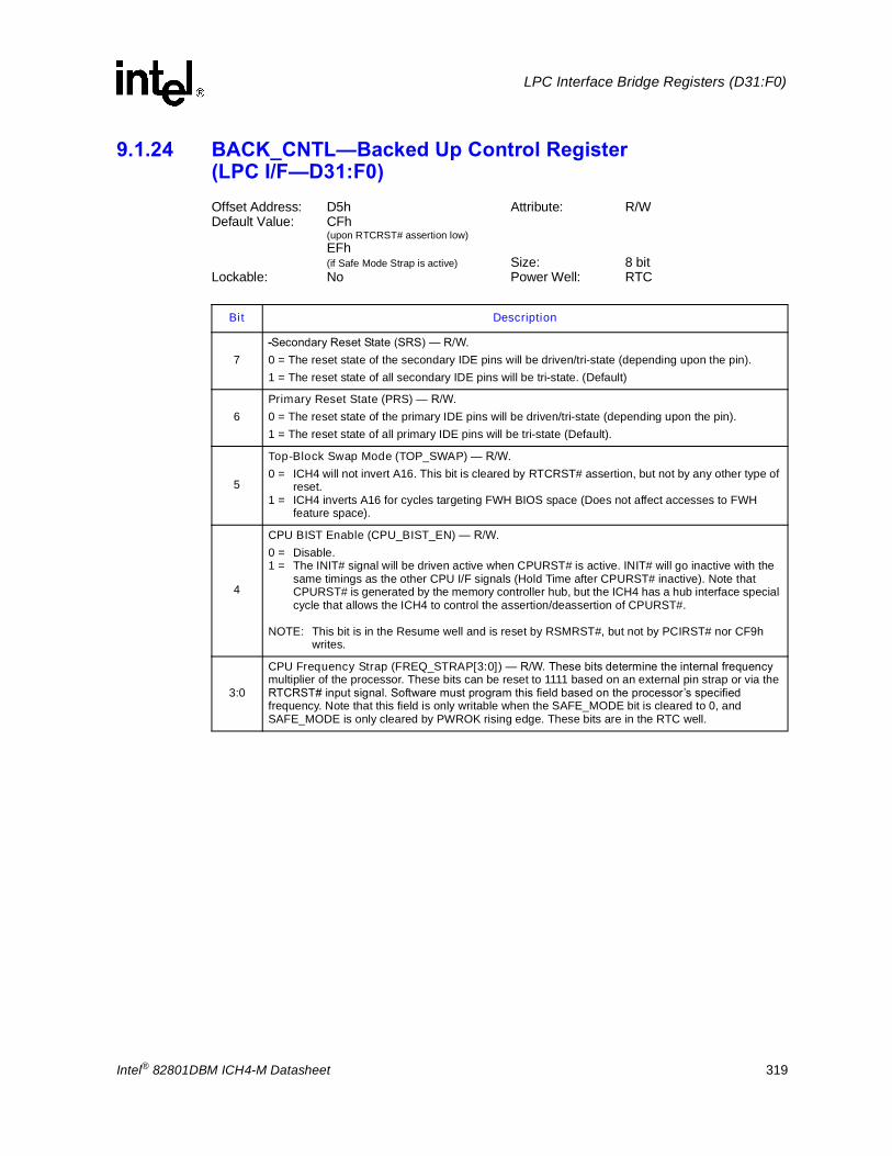
Intel® 82801DBM ICH4-M Datasheet 319
LPC Interface Bridge Registers (D31:F0)
9.1.24 BACK_CNTL�Backed Up Control Register (LPC I/F�D31:F0)Offset Address: D5h Attribute: R/WDefault Value: CFh
(upon RTCRST# assertion low)EFh(if Safe Mode Strap is active) Size: 8 bit
Lockable: No Power Well: RTC
Bit Description
7 Secondary Reset State (SRS) � R/W. 0 = The reset state of the secondary IDE pins will be driven/tri-state (depending upon the pin). 1 = The reset state of all secondary IDE pins will be tri-state. (Default)
6Primary Reset State (PRS) � R/W. 0 = The reset state of the primary IDE pins will be driven/tri-state (depending upon the pin). 1 = The reset state of all primary IDE pins will be tri-state (Default).
5
Top-Block Swap Mode (TOP_SWAP) � R/W.0 = ICH4 will not invert A16. This bit is cleared by RTCRST# assertion, but not by any other type of
reset.1 = ICH4 inverts A16 for cycles targeting FWH BIOS space (Does not affect accesses to FWH
feature space).
4
CPU BIST Enable (CPU_BIST_EN) � R/W.0 = Disable.1 = The INIT# signal will be driven active when CPURST# is active. INIT# will go inactive with the
same timings as the other CPU I/F signals (Hold Time after CPURST# inactive). Note that CPURST# is generated by the memory controller hub, but the ICH4 has a hub interface special cycle that allows the ICH4 to control the assertion/deassertion of CPURST#.
NOTE: This bit is in the Resume well and is reset by RSMRST#, but not by PCIRST# nor CF9h writes.
3:0
CPU Frequency Strap (FREQ_STRAP[3:0]) � R/W. These bits determine the internal frequency multiplier of the processor. These bits can be reset to 1111 based on an external pin strap or via the RTCRST# input signal. Software must program this field based on the processor�s specified frequency. Note that this field is only writable when the SAFE_MODE bit is cleared to 0, and SAFE_MODE is only cleared by PWROK rising edge. These bits are in the RTC well.

320 Intel® 82801DBM ICH4-M Datasheet
LPC Interface Bridge Registers (D31:F0)
9.1.25 RTC_CONF�RTC Configuration Register (LPC I/F�D31:F0)Offset Address: D8h Attribute: R/W, R/W-SpecialDefault Value: 00h Size: 8 bitLockable: Yes Power Well: Core
9.1.26 COM_DEC�LPC I/F Communication Port Decode Ranges (LPC I/F�D31:F0)Offset Address: E0h Attribute: R/WDefault Value: 00h Size: 8 bitLockable: No Power Well: Core
Bit Description
7:5 Reserved
4
Upper 128-byte Lock (U128LOCK) � R/W-Special.0 = Access to these bytes in the upper CMOS RAM range have not been locked.1 = Locks reads and writes to bytes 38h�3Fh in the upper 128-byte bank of the RTC CMOS RAM.
Write cycles to this range will have no effect and read cycles will not return any particular guaranteed value. This is a write once register that can only be reset by a hardware reset.
3
Lower 128-byte Lock (L128LOCK) � R/W-Special.0 = Access to these bytes in the lower CMOS RAM range have not been locked.1 = Locks reads and writes to bytes 38h�3Fh in the lower 128-byte bank of the RTC CMOS RAM.
Write cycles to this range will have no effect and read cycles will not return any particular guaranteed value. This is a write once register that can only be reset by a hardware reset.
2Upper 128-byte Enable (U128E) � R/W.0 = Disable.1 = Enables access to the upper 128-byte bank of RTC CMOS RAM.
1:0 Reserved
Bit Description
7 Reserved
6:4
COMB Decode Range � R/W. This field determines which range to decode for the COMB Port.000 = 3F8h�3FFh (COM1)001 = F8h�2FFh (COM2)010 = 220h�227h011 = 228h�22Fh100 = 238h�23Fh 101 = 2E8h�2EFh (COM4)110 = 338h�33Fh 111 = 3E8h�3EFh (COM3)
3 Reserved
2:0
COMA Decode Range � R/W. This field determines which range to decode for the COMA Port.000 = 3F8h�3FFh (COM1)001 = 2F8h�2FFh (COM2)010 = 220h�227h011 = 228h�22Fh100 = 238h�23Fh 101 = 2E8h�2EFh (COM4)110 = 338h�33Fh 111 = 3E8h�3EFh (COM3)

Intel® 82801DBM ICH4-M Datasheet 321
LPC Interface Bridge Registers (D31:F0)
9.1.27 FDD/LPT_DEC�LPC I/F FDD & LPT Decode Ranges (LPC I/F�D31:F0)Offset Address: E1h Attribute: R/WDefault Value: 00h Size: 8 bitLockable: No Power Well: Core
9.1.28 SND_DEC�LPC I/F Sound Decode Ranges (LPC I/F�D31:F0)Offset Address: E2h Attribute: R/WDefault Value: 00h Size: 8 bitLockable: No Power Well: Core
Bit Description
7:5 Reserved
4FDD Decode Range � R/W. Determines which range to decode for the FDD Port0 = 3F0h�3F5h, 3F7h (Primary)1 = 370h�2FFh (Secondary)
3:2 Reserved
1:0
LPT Decode Range � R/W. This field determines which range to decode for the LPTPort.00 = 378h�37Fh and 778h�77Fh01 = 278h�27Fh (port 279h is read only) and 678h�67Fh10 = 3BCh�3BEh and 7BCh�7BEh11 = Reserved
Bit Description
7:6 Reserved
5:4
MSS Decode Range � R/W. This field determines which range to decode for the Microsoft* Sound System (MSS)00 = 530h�537h01 = 604h�60Bh10 = E80h�E87h11 = F40h�F47h
3MIDI Decode Range � R/W. This bit determines which range to decode for the Midi Port0 = 330h�331h1 = 300h�301h
2 Reserved
1:0
SB16 Decode Range � R/W. This field determines which range to decode for the Sound Blaster 16 (SB16) Port00 = 220h�233h01 = 240h�253h 10 = 260h�273h11 = 280h�293h
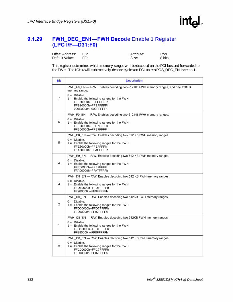
322 Intel® 82801DBM ICH4-M Datasheet
LPC Interface Bridge Registers (D31:F0)
9.1.29 FWH_DEC_EN1�FWH Decode Enable 1 Register (LPC I/F�D31:F0)Offset Address: E3h Attribute: R/WDefault Value: FFh Size: 8 bits
This register determines which memory ranges will be decoded on the PCI bus and forwarded to the FWH. The ICH4 will subtractively decode cycles on PCI unless POS_DEC_EN is set to 1.
Bit Description
7
FWH_F8_EN � R/W. Enables decoding two 512 KB FWH memory ranges, and one 128KB memory range.0 = Disable1 = Enable the following ranges for the FWH
FFF80000h�FFFFFFFFhFFB80000h�FFBFFFFFh000E0000h�000FFFFFh
6
FWH_F0_EN � R/W. Enables decoding two 512 KB FWH memory ranges.0 = Disable.1 = Enable the following ranges for the FWH:
FFF00000h�FFF7FFFFhFFB00000h�FFB7FFFFh
5
FWH_E8_EN � R/W. Enables decoding two 512 KB FWH memory ranges.0 = Disable.1 = Enable the following ranges for the FWH:
FFE80000h�FFEFFFFh FFA80000h�FFAFFFFFh
4
FWH_E0_EN � R/W. Enables decoding two 512 KB FWH memory ranges.0 = Disable.1 = Enable the following ranges for the FWH:
FFE00000h�FFE7FFFFhFFA00000h�FFA7FFFFh
3
FWH_D8_EN � R/W. Enables decoding two 512 KB FWH memory ranges.0 = Disable.1 = Enable the following ranges for the FWH
FFD80000h�FFDFFFFFhFF980000h�FF9FFFFFh
2
FWH_D0_EN � R/W. Enables decoding two 512KB FWH memory ranges.0 = Disable.1 = Enable the following ranges for the FWH
FFD00000h�FFD7FFFFhFF900000h�FF97FFFFh
1
FWH_C8_EN � R/W. Enables decoding two 512KB FWH memory ranges.0 = Disable.1 = Enable the following ranges for the FWH
FFC80000h�FFCFFFFFhFF880000h�FF8FFFFFh
0
FWH_C0_EN � R/W. Enables decoding two 512 KB FWH memory ranges.0 = Disable.1 = Enable the following ranges for the FWH
FFC00000h�FFC7FFFFhFF800000h�FF87FFFFh

Intel® 82801DBM ICH4-M Datasheet 323
LPC Interface Bridge Registers (D31:F0)
9.1.30 GEN1_DEC�LPC I/F Generic Decode Range 1 Register(LPC I/F�D31:F0)Offset Address: E4h�E5h Attribute: R/WDefault Value: 00h Size: 16 bitLockable: Yes Power Well: Core
9.1.31 LPC_EN�LPC I/F Enables Register (LPC I/F�D31:F0)Offset Address: E6h�E7h Attribute: R/WDefault Value: 00h Size: 16 bitLockable: Yes Power Well: Core
Bit Description
15:7Generic I/O Decode Range 1 Base Address (GEN1_BASE) � R/W. This address is aligned on a 128-byte boundary, and must have address lines 31:16 as 0.NOTE: This generic decode is for I/O addresses only, not memory addresses. The size of this
range is 128 bytes.
6:1 Reserved
0Generic Decode Range 1 Enable (GEN1_EN) � R/W. 0 = Disable.1 = Enable the GEN1 I/O range to be forwarded to the LPC I/F
Bit Description
15:14 Reserved
13
CNF2_LPC_EN � R/W.0 = Disable.1 = Enables the decoding of the I/O locations 4Eh and 4Fh to the LPC interface. This range is used
for a microcontroller.
12
CNF1_LPC_EN � R/W.0 = Disable.1 = Enables the decoding of the I/O locations 2Eh and 2Fh to the LPC interface. This range is used
for Super I/O devices.
11
MC_LPC_EN � R/W.0 = Disable.1 = Enables the decoding of the I/O locations 62h and 66h to the LPC interface. This range is used
for a microcontroller.
10
KBC_LPC_EN � R/W. 0 = Disable.1 = Enables the decoding of the I/O locations 60h and 64h to the LPC interface. This range is used
for a microcontroller.
9
GAMEH_LPC_EN � R/W.0 = Disable.1 = Enables the decoding of the I/O locations 208h to 20Fh to the LPC interface. This range is
used for a gameport.
8
GAMEL_LPC_EN � R/W.0 = Disable.1 = Enables the decoding of the I/O locations 200h to 207h to the LPC interface. This range is
used for a gameport.

324 Intel® 82801DBM ICH4-M Datasheet
LPC Interface Bridge Registers (D31:F0)
7ADLIB_LPC_EN � R/W.0 = Disable.1 = Enables the decoding of the I/O locations 388h�38Bh to the LPC interface.
6
MSS_LPC_EN � R/W.0 = Disable.1 = Enables the decoding of the MSS range to the LPC interface. This range is selected in the
LPC_Sound Decode Range Register.
5
MIDI_LPC_EN � R/W.0 = Disable.1 = Enables the decoding of the MIDI range to the LPC interface. This range is selected in the
LPC_Sound Decode Range Register.
4
SB16_LPC_EN � R/W.0 = Disable.1 = Enables the decoding of the SB16 range to the LPC interface. This range is selected in the
LPC_Sound Decode Range Register.
3
FDD_LPC_EN � R/W.0 = Disable.1 = Enables the decoding of the FDD range to the LPC interface. This range is selected in the
LPC_FDD/LPT Decode Range Register.
2
LPT_LPC_EN � R/W.0 = Disable.1 = Enables the decoding of the LPTrange to the LPC interface. This range is selected in the
LPC_FDD/LPT Decode Range Register.
1
COMB_LPC_EN � R/W.0 = Disable.1 = Enables the decoding of the COMB range to the LPC interface. This range is selected in the
LPC_COM Decode Range Register.
0
COMA_LPC_EN � R/W.0 = Disable.1 = Enables the decoding of the COMA range to the LPC interface. This range is selected in the
LPC_COM Decode Range Register.
Bit Description

Intel® 82801DBM ICH4-M Datasheet 325
LPC Interface Bridge Registers (D31:F0)
9.1.32 FWH_SEL1�FWH Select 1 Register (LPC I/F�D31:F0)Offset Address: E8h Attribute: R/W, RODefault Value: 00112233h Size: 32 bits
Bit Description
31:28
FWH_F8_IDSEL � RO. IDSEL for two 512 KB FWH memory ranges and one 128 KB memory range. This field is fixed at 0000. The IDSEL programmed in this field addresses the following memory ranges:FFF8 0000h�FFFF FFFFhFFB8 0000h�FFBF FFFFh000E 0000h�000F FFFFh
27:24
FWH_F0_IDSEL � R/W. IDSEL for two 512 KB FWH memory ranges. The IDSEL programmed in this field addresses the following memory ranges:FFF0 0000h�FFF7 FFFFhFFB0 0000h�FFB7 FFFFh
23:20
FWH_E8_IDSEL � R/W. IDSEL for two 512 KB FWH memory ranges. The IDSEL programmed in this field addresses the following memory ranges:FFE8 0000h�FFEF FFFFh FFA8 0000h�FFAF FFFFh
19:16
FWH_E0_IDSEL � R/W. IDSEL for two 512 KB FWH memory ranges. The IDSEL programmed in this field addresses the following memory ranges:FFE0 0000h�FFE7 FFFFhFFA0 0000h�FFA7 FFFFh
15:12
FWH_D8_IDSEL � R/W. IDSEL for two 512 KB FWH memory ranges. The IDSEL programmed in this field addresses the following memory ranges:FFD8 0000h�FFDF FFFFhFF98 0000h�FF9F FFFFh
11:8
FWH_D0_IDSEL � R/W. IDSEL for two 512 KB FWH memory ranges. The IDSEL programmed in this field addresses the following memory ranges:FFD0 0000h�FFD7 FFFFhFF90 0000h�FF97 FFFFh
7:4
FWH_C8_IDSEL � R/W. IDSEL for two 512 KB FWH memory ranges. The IDSEL programmed in this field addresses the following memory ranges:FFC8 0000h�FFCF FFFFhFF88 0000h�FF8F FFFFh
3:0
FWH_C0_IDSEL � R/W. IDSEL for two 512 KB FWH memory ranges. The IDSEL programmed in this field addresses the following memory ranges:FFC0 0000h�FFC7 FFFFhFF80 0000h�FF87 FFFFh

326 Intel® 82801DBM ICH4-M Datasheet
LPC Interface Bridge Registers (D31:F0)
9.1.33 GEN2_DEC�LPC I/F Generic Decode Range 2 Register(LPC I/F�D31:F0)Offset Address: ECh�EDh Attribute: R/WDefault Value: 00h Size: 16 bitLockable: Yes Power Well: Core
9.1.34 FWH_SEL2�FWH Select 2 Register (LPC I/F�D31:F0)Offset Address: EEh�EFh Attribute: R/WDefault Value: 4567h Size: 32 bits
Bit Description
15:4
Generic I/O Decode Range 2 Base Address (GEN2_BASE) � R/W. This address is aligned on a 64-byte boundary, and must have address lines 31:16 as 0.Note that this generic decode is for I/O addresses only, not memory addresses. The size of this range is 16 bytes.
3:1 Reserved. Read as 0
0Generic I/O Decode Range 2 Enable (GEN2_EN) � R/W. 0 = Disable.1 = Accesses to the GEN2 I/O range will be forwarded to the LPC I/F
Bit Description
15:12
FWH_70_IDSEL � R/W. IDSEL for two 1M FWH memory ranges. The IDSEL programmed in this field addresses the following memory ranges:FF70 0000h�FF7F FFFFhFF30 0000h�FF3F FFFFh
11:8
FWH_60_IDSEL � R/W. IDSEL for two 1M FWH memory ranges. The IDSEL programmed in this field addresses the following memory ranges:FF60 0000h�FF6F FFFFh FF20 0000h�FF2F FFFFh
7:4
FWH_50_IDSEL � R/W. IDSEL for two 1M FWH memory ranges. The IDSEL programmed in this field addresses the following memory ranges:FF50 0000h�FF5F FFFFhFF10 0000h�FF1F FFFFh
3:0
FWH_40_IDSEL � R/W. IDSEL for two 1M FWH memory ranges. The IDSEL programmed in this field addresses the following memory ranges:FF40 0000h�FF4F FFFFhFF00 0000h�FF0F FFFFh

Intel® 82801DBM ICH4-M Datasheet 327
LPC Interface Bridge Registers (D31:F0)
9.1.35 FWH_DEC_EN2�FWH Decode Enable 2 Register (LPC I/F�D31:F0)Offset Address: F0h Attribute: R/WDefault Value: 0Fh Size: 8 bits
This register determines which memory ranges will be decoded on the PCI bus and forwarded to the FWH. The ICH4 will subtractively decode cycles on PCI unless POS_DEC_EN is set to 1.
Bit Description
7:4 Reserved
3
FWH_70_EN � R/W. Enables decoding two 1M FWH memory ranges.0 = Disable.1 = Enable the following ranges for the FWH
FF70 0000h�FF7F FFFFhFF30 0000h�FF3F FFFFh
2
FWH_60_EN � R/W. Enables decoding two 1M FWH memory ranges.0 = Disable.1 = Enable the following ranges for the FWH
FF60 0000h�FF6F FFFFh FF20 0000h�FF2F FFFFh
1
FWH_50_EN � R/W. Enables decoding two 1M FWH memory ranges.0 = Disable.1 = Enable the following ranges for the FWH
FF50 0000h�FF5F FFFFhFF10 0000h�FF1F FFFFh
0
FWH_40_EN � R/W. Enables decoding two 1M FWH memory ranges.0 = Disable.1 = Enable the following ranges for the FWH
FF40 0000h�FF4F FFFFhFF00 0000h�FF0F FFFFh

328 Intel® 82801DBM ICH4-M Datasheet
LPC Interface Bridge Registers (D31:F0)
9.1.36 FUNC_DIS�Function Disable Register (LPC I/F�D31:F0)Offset Address: F2h Attribute: R/WDefault Value: 00h Size: 16 bitsLockable: No Power Well: Core
Bit Description
15
D29_F7_Disable � R/W. Software sets this bit to disable the USB EHCI Controller function. BIOS must not enable I/O or memory address space decode, interrupt generation, or any other functionality of functions that are to be disabled.0 = Enable. USB EHCI Controller is enabled1 = Disable. USB EHCI Controller is disabled
14
LPC Bridge Disable (D31F0D) � R/W. 0 = Enable. 1 = Disable LPC bridge. When disabled, the following spaces will no longer be decoded by the LPC
bridge:� Device 31, Function 0 Configuration space� Memory cycles below 16 MB (100000h)� I/O cycles below 64 KB (100h)� The Internal I/OxAPIC at FEC0_0000 to FECF_FFFFMemory cycles in the LPC BIOS range below 4GB will still be decoded when this bit is set, but the aliases at the top of 1 MB (the E and F segment) no longer will be decoded.
13:11 Reserved
10
D29_F2_Disable � R/W. Software sets this bit to disable the USB UHCI Controller #3 function. BIOS must not enable I/O or memory address space decode, interrupt generation, or any other functionality of functions that are to be disabled.0 = Enable. USB UHCI Controller #3 is enabled1 = Disable. USB UHCI Controller #3 is disabled
9
D29_F1_Disable � R/W. Software sets this bit to disable the USB UHCI Controller #2 function. BIOS must not enable I/O or memory address space decode, interrupt generation, or any other functionality of functions that are to be disabled.0 = Enable. USB UHCI Controller #2 is enabled1 = Disable. USB UHCI Controller #2 is disabled
8
D29_F0_Disable � R/W. Software sets this bit to disable the USB UHCI Controller #1 function.BIOS must not enable I/O or memory address space decode, interrupt generation, or any other functionality of functions that are to be disabled.0 = Enable. USB UHCI Controller #1 is enabled1 = Disable. USB UHCI Controller #1 is disabled
7 Reserved
6
D31_F6_Disable � R/W. Software sets this bit to disable the AC�97 modem controller function. BIOS must not enable I/O or memory address space decode, interrupt generation, or any other functionality of functions that are to be disabled.0 = Enable. AC�97 Modem is enabled1 = Disable. AC�97 Modem is disabled
5
D31_F5_Disable � R/W. Software sets this bit to disable the AC�97 audio controller function. BIOS must not enable I/O or memory address space decode, interrupt generation, or any other functionality of functions that are to be disabled.0 = Enable. AC �97 audio controller is enabled1 = Disable. AC �97 audio controller is disabled
4 Reserved

Intel® 82801DBM ICH4-M Datasheet 329
LPC Interface Bridge Registers (D31:F0)
NOTES:1. Software must always disable all functionality within the function before disabling the configuration space.2. Configuration writes to internal ICH4 USB EHCI (D29:F7) and AC �97 (D31:F5, F6) devices when disabled
are illegal and may cause undefined results.
3
D31_F3_Disable � R/W. Software sets this bit to disable the SMBus Host Controller function. BIOS must not enable I/O or memory address space decode, interrupt generation, or any other functionality of functions that are to be disabled.0 = Enable. SMBus controller is enabled1 = Disable. SMBus controller is disabled
2 Reserved
1
D31_F1_Disable � R/W. Software sets this bit to disable the IDE controller function. BIOS must not enable I/O or memory address space decode, interrupt generation, or any other functionality of functions that are to be disabled.0 = Enable. IDE controller is enabled1 = Disable. IDE controller is disabled
0
SMB_FOR_BIOS � R/W. This bit is used in conjunction with bit 3 in this register.0 = No effect.1 = Allows the SMBus I/O space to be accessible by software when bit 3 in this register is set. The
PCI configuration space is hidden in this case. Note that if bit 3 is set alone, the decode of both SMBus PCI configuration and I/O space will be disabled.
Bit Description

330 Intel® 82801DBM ICH4-M Datasheet
LPC Interface Bridge Registers (D31:F0)
9.2 DMA I/O Registers
Table 9-2. DMA Registers Port Alias Register Name Default Type00h 10h Channel 0 DMA Base & Current Address Register Undefined R/W01h 11h Channel 0 DMA Base & Current Count Register Undefined R/W02h 12h Channel 1 DMA Base & Current Address Register Undefined R/W03h 13h Channel 1 DMA Base & Current Count Register Undefined R/W04h 14h Channel 2 DMA Base & Current Address Register Undefined R/W05h 15h Channel 2 DMA Base & Current Count Register Undefined R/W06h 16h Channel 3 DMA Base & Current Address Register Undefined R/W07h 17h Channel 3 DMA Base & Current Count Register Undefined R/W
08h 18hChannel 0�3 DMA Command Register Undefined WOChannel 0�3 DMA Status Register Undefined RO
0Ah 1Ah Channel 0�3 DMA Write Single Mask Register 000001XXb WO0Bh 1Bh Channel 0�3 DMA Channel Mode Register 000000XXb WO0Ch 1Ch Channel 0�3 DMA Clear Byte Pointer Register Undefined WO0Dh 1Dh Channel 0�3 DMA Master Clear Register Undefined WO0Eh 1Eh Channel 0�3 DMA Clear Mask Register Undefined WO0Fh 1Fh Channel 0�3 DMA Write All Mask Register 0Fh R/W80h 90h Reserved Page Register Undefined R/W81h 91h Channel 2 DMA Memory Low Page Register Undefined R/W82h � Channel 3 DMA Memory Low Page Register Undefined R/W83h 93h Channel 1 DMA Memory Low Page Register Undefined R/W
84h�86h 94h�96h Reserved Page Registers Undefined R/W87h 97h Channel 0 DMA Memory Low Page Register Undefined R/W88h 98h Reserved Page Register Undefined R/W89h 99h Channel 6 DMA Memory Low Page Register Undefined R/W8Ah 9Ah Channel 7 DMA Memory Low Page Register Undefined R/W8Bh 9Bh Channel 5 DMA Memory Low Page Register Undefined R/W
8Ch�8Eh 9Ch�9Eh Reserved Page Registers Undefined R/W8Fh 9Fh Refresh Low Page Register Undefined R/WC0h C1h Channel 4 DMA Base & Current Address Register Undefined R/WC2h C3h Channel 4 DMA Base & Current Count Register Undefined R/WC4h C5h Channel 5 DMA Base & Current Address Register Undefined R/WC6h C7h Channel 5 DMA Base & Current Count Register Undefined R/WC8h C9h Channel 6 DMA Base & Current Address Register Undefined R/WCAh CBh Channel 6 DMA Base & Current Count Register Undefined R/WCCh CDh Channel 7 DMA Base & Current Address Register Undefined R/WCEh CFh Channel 7 DMA Base & Current Count Register Undefined R/W
D0h D1hChannel 4�7 DMA Command Register Undefined WOChannel 4�7 DMA Status Register Undefined RO
D4h D5h Channel 4�7 DMA Write Single Mask Register 000001XXb WOD6h D7h Channel 4�7 DMA Channel Mode Register 000000XXb WOD8h D9h Channel 4�7 DMA Clear Byte Pointer Register Undefined WODAh DBh Channel 4�7 DMA Master Clear Register Undefined WODCh DDh Channel 4�7 DMA Clear Mask Register Undefined WODEh DFh Channel 4�7 DMA Write All Mask Register 0Fh R/W

Intel® 82801DBM ICH4-M Datasheet 331
LPC Interface Bridge Registers (D31:F0)
9.2.1 DMABASE_CA�DMA Base and Current Address RegistersI/O Address: Ch. #0 = 00h; Ch. #1 = 02h Attribute: R/W
Ch. #2 = 04h; Ch. #3 = 06h Size: 16 bit (per channel), Ch. #5 = C4h Ch. #6 = C8h but accessed in two 8-bit Ch. #7 = CCh; quantities
Default Value: UndefLockable: No Power Well: Core
9.2.2 DMABASE_CC�DMA Base and Current Count RegistersI/O Address: Ch. #0: = 01h; Ch. #1 = 03h Attribute: R/W
Ch. #2: = 05h; Ch. #3 = 07h Size: 16 bit (per channel),Ch. #5 = C6h; Ch. #6 = CAh but accessed in two 8-bit Ch. #7 = CEh; quantities
Default Value: Undefined Lockable: No Power Well: Core
Bit Description
15:0
Base and Current Address � R/W. This register determines the address for the transfers to be performed. The address specified points to two separate registers. On writes, the value is stored in the Base Address register and copied to the Current Address register. On reads, the value is returned from the Current Address register.The address increments/decrements in the Current Address register after each transfer, depending on the mode of the transfer. If the channel is in auto-initialize mode, the Current Address register will be reloaded from the Base Address register after a terminal count is generated.For transfers to/from a 16-bit slave (channel�s 5�7), the address is shifted left one bit location. Bit 15 will be shifted into Bit 16.The register is accessed in 8 bit quantities. The byte is pointed to by the current byte pointer flip/flop. Before accessing an address register, the byte pointer flip/flop should be cleared to ensure that the low byte is accessed first
Bit Description
15:0
Base and Current Count � R/W. This register determines the number of transfers to be performed. The address specified points to two separate registers. On writes, the value is stored in the Base Count register and copied to the Current Count register. On reads, the value is returned from the Current Count register.The actual number of transfers is one more than the number programmed in the Base Count Register (i.e., programming a count of 4h results in 5 transfers). The count is decrements in the Current Count register after each transfer. When the value in the register rolls from zero to FFFFh, a terminal count is generated. If the channel is in auto-initialize mode, the Current Count register will be reloaded from the Base Count register after a terminal count is generated.For transfers to/from an 8-bit slave (channels 0�3), the count register indicates the number of bytes to be transferred. For transfers to/from a 16-bit slave (channels 57), the count register indicates the number of words to be transferred.The register is accessed in 8 bit quantities. The byte is pointed to by the current byte pointer flip/flop. Before accessing a count register, the byte pointer flip/flop should be cleared to ensure that the low byte is accessed first.

332 Intel® 82801DBM ICH4-M Datasheet
LPC Interface Bridge Registers (D31:F0)
9.2.3 DMAMEM_LP�DMA Memory Low Page RegistersI/O Address: Ch. #0 = 87h; Ch. #1 = 83h
Ch. #2 = 81h; Ch. #3 = 82hCh. #5 = 8Bh; Ch. #6 = 89hCh. #7 = 8Ah; Attribute: R/W
Default Value: Undefined Size: 8 bitLockable: No Power Well: Core
9.2.4 DMACMD�DMA Command RegisterI/O Address: Ch. #0�3 = 08h;
Ch. #4�7 = D0h Attribute: WODefault Value: Undefined Size: 8 bitLockable: No Power Well: Core
Bit Description
7:0
DMA Low Page (ISA Address bits [23:16]) � R/W. This register works in conjunction with the DMA controller's Current Address Register to define the complete 24-bit address for the DMA channel. This register remains static throughout the DMA transfer. Bit 16 of this register is ignored when in 16 bit I/O count by words mode as it is replaced by the bit 15 shifted out from the current address register.
Bit Description
7:5 Reserved. Must be 0.
4
DMA Group Arbitration Priority � WO. Each channel group is individually assigned either fixed or rotating arbitration priority. At part reset, each group is initialized in fixed priority. 0 = Fixed priority to the channel group1 = Rotating priority to the group.
3 Reserved. Must be 0
2
DMA Channel Group Enable � WO. Both channel groups are enabled following part reset.0 = Enable the DMA channel group.1 = Disable. Disabling channel group 4�7 also disables channel group 0�3, which is cascaded
through channel 4.
1:0 Reserved. Must be 0.

Intel® 82801DBM ICH4-M Datasheet 333
LPC Interface Bridge Registers (D31:F0)
9.2.5 DMASTA�DMA Status RegisterI/O Address: Ch. #0�3 = 08h;
Ch. #4�7 = D0h Attribute: RODefault Value: Undefined Size: 8 bitLockable: No Power Well: Core
9.2.6 DMA_WRSMSK�DMA Write Single Mask RegisterI/O Address: Ch. #0�3 = 0Ah;
Ch. #4�7 = D4h Attribute: WODefault Value: 0000 01xx Size: 8 bitLockable: No Power Well: Core
Bit Description
7:4
Channel Request Status � RO. When a valid DMA request is pending for a channel, the corresponding bit is set to 1. When a DMA request is not pending for a particular channel, the corresponding bit is set to 0. The source of the DREQ may be hardware or a software request. Note that channel 4 is the cascade channel, so the request status of channel 4 is a logical OR of the request status for channels 0 through 3.4 = Channel 0 5 = Channel 1 (5)6 = Channel 2 (6)7 = Channel 3 (7)
3:0
Channel Terminal Count Status � RO. When a channel reaches terminal count (TC), its status bit is set to 1. If TC has not been reached, the status bit is set to 0. Channel 4 is programmed for cascade, so the TC bit response for channel 4 is irrelevant:0 = Channel 0 1 = Channel 1 (5)2 = Channel 2 (6)3 = Channel 3 (7)
Bit Description
7:3 Reserved. Must be 0.
2
Channel Mask Select � WO.0 = Enable DREQ for the selected channel. The channel is selected through bits [1:0]. Therefore,
only one channel can be masked / unmasked at a time.1 = Disable DREQ for the selected channel.
1:0
DMA Channel Select � WO. These bits select the DMA Channel Mode Register to program.00 = Channel 0 (4)01 = Channel 1 (5)10 = Channel 2 (6) 11 = Channel 3 (7)

334 Intel® 82801DBM ICH4-M Datasheet
LPC Interface Bridge Registers (D31:F0)
9.2.7 DMACH_MODE�DMA Channel Mode RegisterI/O Address: Ch. #0�3 = 0Bh;
Ch. #4�7 = D6h Attribute: WODefault Value: 0000 00xx Size: 8 bitLockable: No Power Well: Core
9.2.8 DMA Clear Byte Pointer RegisterI/O Address: Ch. #0�3 = 0Ch;
Ch. #4�7 = D8h Attribute: WODefault Value: xxxx xxxx Size: 8 bitLockable: No Power Well: Core
Bit Description
7:6
DMA Transfer Mode � WO. Each DMA channel can be programmed in one of four different modes: 00 = Demand mode01 = Single mode10 = Reserved11 = Cascade mode
5
Address Increment/Decrement Select � WO. This bit controls address increment/decrement during DMA transfers. 0 = Address increment. (default after part reset or Master Clear)1 = Address decrement.
4
Autoinitialize Enable � WO.0 = Autoinitialize feature is disabled and DMA transfers terminate on a terminal count. A part reset or
Master Clear disables autoinitialization.1 = DMA restores the Base Address and Count registers to the current registers following a terminal
count (TC).
3:2
DMA Transfer Type � WO. These bits represent the direction of the DMA transfer. When the channel is programmed for cascade mode, (bits[7:6] = 11) the transfer type is irrelevant.00 = Verify: No I/O or memory strobes generated01 = Write: Data transferred from the I/O devices to memory10 = Read: Data transferred from memory to the I/O device11 = Illegal
1:0
DMA Channel Select � WO. These bits select the DMA Channel Mode Register that will be written by bits [7:2].00 = Channel 0 (4)01 = Channel 1 (5)10 = Channel 2 (6)11 = Channel 3 (7)
Bit Description
7:0
Clear Byte Pointer � WO. No specific pattern. Command enabled with a write to the I/O port address. Writing to this register initializes the byte pointer flip/flop to a known state. It clears the internal latch used to address the upper or lower byte of the 16-bit Address and Word Count Registers. The latch is also cleared by part reset and by the Master Clear command. This command precedes the first access to a 16-bit DMA controller register. The first access to a 16-bit register will then access the significant byte, and the second access automatically accesses the most significant byte.

Intel® 82801DBM ICH4-M Datasheet 335
LPC Interface Bridge Registers (D31:F0)
9.2.9 DMA Master Clear RegisterI/O Address: Ch. #0�3 = 0Dh;
Ch. #4�7 = DAh Attribute: WODefault Value: xxxx xxxx Size: 8 bit
9.2.10 DMA_CLMSK�DMA Clear Mask RegisterI/O Address: Ch. #0�3 = 0Eh;
Ch. #4�7 = DCh Attribute: WODefault Value: xxxx xxxx Size: 8 bitLockable: No Power Well: Core
9.2.11 DMA_WRMSK�DMA Write All Mask RegisterI/O Address: Ch. #0�3 = 0Fh;
Ch. #4�7 = DEh Attribute: R/WDefault Value: 0000 1111 Size: 8 bitLockable: No Power Well: Core
Bit Description
7:0Master Clear � WO. No specific pattern. Enabled with a write to the port. This has the same effect as the hardware Reset. The Command, Status, Request, and Byte Pointer flip/flop registers are cleared and the Mask Register is set.
Bit Description
7:0 Clear Mask Register � WO. No specific pattern. Command enabled with a write to the port.
Bit Description
7:4 Reserved. Must be 0.
3:0
Channel Mask Bits � R/W. This register permits all four channels to be simultaneously enabled/disabled instead of enabling/disabling each channel individually, as is the case with the Mask Register - Write Single Mask Bit. In addition, this register has a read path to allow the status of the channel mask bits to be read. A channel's mask bit is automatically set to 1 when the Current Byte/Word Count Register reaches terminal count (unless the channel is in auto-initialization mode).Setting the bit(s) to a 1 disables the corresponding DREQ(s). Setting the bit(s) to a 0 enables the corresponding DREQ(s). Bits [3:0] are set to 1 upon part reset or Master Clear. When read, bits [3:0] indicate the DMA channel [3:0] ([7:4]) mask status. Bit 0 = Channel 0 (4)1 = Masked, 0 = Not MaskedBit 1 = Channel 1 (5)1 = Masked, 0 = Not MaskedBit 2 = Channel 2 (6)1 = Masked, 0 = Not MaskedBit 3 = Channel 3 (7)1 = Masked, 0 = Not Masked
NOTE: Disabling channel 4 also disables channels 0�3 due to the cascade of channel�s 0�3 through channel 4.

336 Intel® 82801DBM ICH4-M Datasheet
LPC Interface Bridge Registers (D31:F0)
9.3 Timer I/O Registers
9.3.1 TCW�Timer Control Word RegisterI/O Address: 43h Default Value: All bits undefinedAttribute: WO Size: 8 bits
This register is programmed prior to any counter being accessed to specify counter modes. Following part reset, the control words for each register are undefined and each counter output is 0. Each timer must be programmed to bring it into a known state.
There are two special commands that can be issued to the counters through this register, the Read Back Command and the Counter Latch Command. When these commands are chosen, several bits within this register are redefined. These register formats are described below.
Port Aliases Register Name/Function Default Value Type
40h 50hCounter 0 Interval Time Status Byte Format 0XXXXXXXb ROCounter 0 Counter Access Port Register Undefined R/W
41h 51hCounter 1 Interval Time Status Byte Format 0XXXXXXXb ROCounter 1 Counter Access Port Register Undefined R/W
42h 52hCounter 2 Interval Time Status Byte Format 0XXXXXXXb RO
Counter 2 Counter Access Port Register Undefined R/W
43h 53hTimer Control Word Register Undefined WOTimer Control Word Register Read Back XXXXXXX0b WO
Counter Latch Command X0h WO
Bit Description
7:6
Counter Select � WO. The Counter Selection bits select the counter the control word acts upon as shown below. The Read Back Command is selected when bits[7:6] are both 1.00 = Counter 0 select01 = Counter 1 select10 = Counter 2 select11 = Read Back Command
5:4
Read/Write Select � WO. These bits are the read/write control bits. The actual counter programming is done through the counter port (40h for counter 0, 41h for counter 1, and 42h for counter 2).00 = Counter Latch Command 01 = Read/Write Least Significant Byte (LSB)10 = Read/Write Most Significant Byte (MSB)11 = Read/Write LSB then MSB
3:1
Counter Mode Selection � WO. These bits select one of six possible modes of operation for the selected counter. 000 = Mode 0Out signal on end of count (=0)001 = Mode 1Hardware retriggerable one-shotx10 = Mode 2Rate generator (divide by n counter)x11 = Mode 3Square wave output100 = Mode 4Software triggered strobe101 = Mode 5Hardware triggered strobe
0Binary/BCD Countdown Select � WO.0 = Binary countdown is used. The largest possible binary count is 2161 = Binary coded decimal (BCD) count is used. The largest possible BCD count is 104

Intel® 82801DBM ICH4-M Datasheet 337
LPC Interface Bridge Registers (D31:F0)
9.3.1.1 RDBK_CMD�Read Back Command
The Read Back Command is used to determine the count value, programmed mode, and current states of the OUT pin and Null count flag of the selected counter or counters. Status and/or count may be latched in any or all of the counters by selecting the counter during the register write. The count and status remain latched until read, and further latch commands are ignored until the count is read. Both count and status of the selected counters may be latched simultaneously by setting both bit 5 and bit 4 to 0. If both are latched, the first read operation from that counter returns the latched status. The next one or two reads, depending on whether the counter is programmed for one or two byte counts, returns the latched count. Subsequent reads return an unlatched count.
9.3.1.2 LTCH_CMD�Counter Latch Command
The Counter Latch Command latches the current count value. This command is used to insure that the count read from the counter is accurate. The count value is then read from each counter's count register through the Counter Ports Access Ports Register (40h for counter 0, 41h for counter 1, and 42h for counter 2). The count must be read according to the programmed format, i.e. if the counter is programmed for two byte counts, two bytes must be read. The two bytes do not have to be read one right after the other (read, write, or programming operations for other counters may be inserted between the reads). If a counter is latched once and then latched again before the count is read, the second Counter Latch Command is ignored.
Bit Description
7:6 Read Back Command. Must be 11 to select the Read Back Command
5Latch Count of Selected Counters.0 = Current count value of the selected counters will be latched1 = Current count will not be latched
4Latch Status of Selected Counters.0 = Status of the selected counters will be latched1 = Status will not be latched
3 Counter 2 Select. 1 = Counter 2 count and/or status will be latched
2 Counter 1 Select. 1 = Counter 1 count and/or status will be latched
1 Counter 0 Select. 1 = Counter 0 count and/or status will be latched.
0 Reserved. Must be 0.
Bit Description
7:6
Counter Selection. These bits select the counter for latching. If 11 is written, then the write is interpreted as a read back command.00 = Counter 001 = Counter 110 = Counter 2
5:4Counter Latch Command.00 = Selects the Counter Latch Command.Others = Reserved
3:0 Reserved. Must be 0.

338 Intel® 82801DBM ICH4-M Datasheet
LPC Interface Bridge Registers (D31:F0)
9.3.2 SBYTE_FMT�Interval Timer Status Byte Format RegisterI/O Address: Counter 0 = 40h,
Counter 1 = 41h, Attribute: ROCounter 2 = 42h Size: 8 bits per counter
Default Value: Bits[6:0] undefined, Bit 7=0
Each counter's status byte can be read following a Read Back Command. If latch status is chosen (bit 4=0, Read Back Command) as a read back option for a given counter, the next read from the counter's Counter Access Ports Register (40h for counter 0, 41h for counter 1, and 42h for counter 2) returns the status byte. The status byte returns the following:
9.3.3 Counter Access Ports RegisterI/O Address: Counter 0�40h,
Counter 1�41h, Attribute: R/WCounter 2�42h
Default Value: All bits undefined Size: 8 bit
Bit Description
7Counter OUT Pin State � RO.0 = OUT pin of the counter is also a 0.1 = OUT pin of the counter is also a 1.
6
Count Register Status � RO. This bit indicates when the last count written to the Count Register (CR) has been loaded into the counting element (CE). The exact time this happens depends on the counter mode, but until the count is loaded into the counting element (CE), the count value will be incorrect.0 = Count has been transferred from CR to CE and is available for reading.1 = Null Count. Count has not been transferred from CR to CE and is not yet available for reading.
5:4
Read/Write Selection Status � RO. These reflect the read/write selection made through bits[5:4] of the control register. The binary codes returned during the status read match the codes used to program the counter read/write selection.00 = Counter Latch Command01 = Read/Write Least Significant Byte (LSB)10 = Read/Write Most Significant Byte (MSB)11 = Read/Write LSB then MSB
3:1
Mode Selection Status � RO. These bits return the counter mode programming. The binary code returned matches the code used to program the counter mode, as listed under the bit function above.000 = Mode 0Out signal on end of count (=0)001 = Mode 1Hardware retriggerable one-shotx10 = Mode 2Rate generator (divide by n counter)x11 = Mode 3Square wave output100 = Mode 4Software triggered strobe101 = Mode 5Hardware triggered strobe
0Countdown Type Status � RO. This bit reflects the current countdown type.0 = Binary countdown 1 = Binary Coded Decimal (BCD) countdown.
Bit Description
7:0Counter Port � R/W. Each counter port address is used to program the 16-bit Count Register. The order of programming, either LSB only, MSB only, or LSB then MSB, is defined with the Interval Counter Control Register at port 43h. The counter port is also used to read the current count from the Count Register, and return the status of the counter programming following a Read Back Command.

Intel® 82801DBM ICH4-M Datasheet 339
LPC Interface Bridge Registers (D31:F0)
9.4 8259 Interrupt Controller (PIC) RegistersThe interrupt controller registers are located at 20h and 21h for the master controller (IRQ0�7), and at A0h and A1h for the slave controller (IRQ8�13). These registers have multiple functions, depending upon the data written to them. Below is a description of the different register possibilities for each address. Table 9-3 provides the register I/O map for the interrupt controller.
Table 9-3. Interrupt Controller I/O Address Map (PIC Registers)
Port Aliases Register Name/Function Default Value Type
20h24h, 28h,2Ch, 30h,
34h, 38h, 3Ch
Master PIC ICW1 Init. Cmd Word 1 Register Undefined WO
Master PIC OCW2 Op Ctrl Word 2 Register 001XXXXXb WO
Master PIC OCW3 Op Ctrl Word 3 Register X01XXX10b R/W
21h25h, 29h, 2Dh, 31h,
35h, 39h, 3Dh
Master PIC ICW2 Init. Cmd Word 2 Register Undefined WO
Master PIC ICW3 Init. Cmd Word 3 Register Undefined WO
Master PIC ICW4 Init. Cmd Word 4 Register 01h WO
Master PIC OCW1 Op Ctrl Word 1 Register 00h R/W
A0hA4h, A8h, ACh, B0h,
B4h, B8h, BCh
Slave PIC ICW1 Init. Cmd Word 1 Register Undefined WO
Slave PIC OCW2 Op Ctrl Word 2 Register 001XXXXXb WO
Slave PIC OCW3 Op Ctrl Word 3 Register X01XXX10b R/W
A1hA5h, A9h,ADh, B1h,
B5h, B9h, BDh
Slave PIC ICW2 Init. Cmd Word 2 Register Undefined WO
Slave PIC ICW3 Init. Cmd Word 3 Register Undefined WO
Slave PIC ICW4 Init. Cmd Word 4 Register 01h WO
Slave PIC OCW1 Op Ctrl Word 1 Register 00h R/W
4D0h � Master PIC Edge/Level Triggered Register 00h R/W
4D1h � Slave PIC Edge/Level Triggered Register 00h R/W

340 Intel® 82801DBM ICH4-M Datasheet
LPC Interface Bridge Registers (D31:F0)
9.4.1 ICW1�Initialization Command Word 1 RegisterOffset Address: Master Controller�020h Attribute: WO Slave Controller�0A0h Size: 8 bit /controllerDefault Value: All bits undefined
A write to Initialization Command Word 1 starts the interrupt controller initialization sequence, during which the following occurs:
1. The Interrupt Mask register is cleared.
2. IRQ7 input is assigned priority 7.
3. The slave mode address is set to 7.
4. Special mask mode is cleared and Status Read is set to IRR.
Once this write occurs, the controller expects writes to ICW2, ICW3, and ICW4 to complete the initialization sequence.
Bit Description
7:5ICW/OCW Select � WO. These bits are MCS-85 specific, and not needed. 000 = Should be programmed to 000
4ICW/OCW Select � WO.1 = This bit must be a 1 to select ICW1 and enable the ICW2, ICW3, and ICW4 sequence.
3 Edge/Level Bank Select (LTIM) � WO. Disabled. Replaced by the edge/level triggered control registers (ELCR).
2ADI � WO.0 = Ignored for the ICH4. Should be programmed to 0.
1Single or Cascade (SNGL) � WO.0 = Must be programmed to a 0 to indicate two controllers operating in cascade mode.
0ICW4 Write Required (IC4) � WO.1 = This bit must be programmed to a 1 to indicate that ICW4 needs to be programmed.
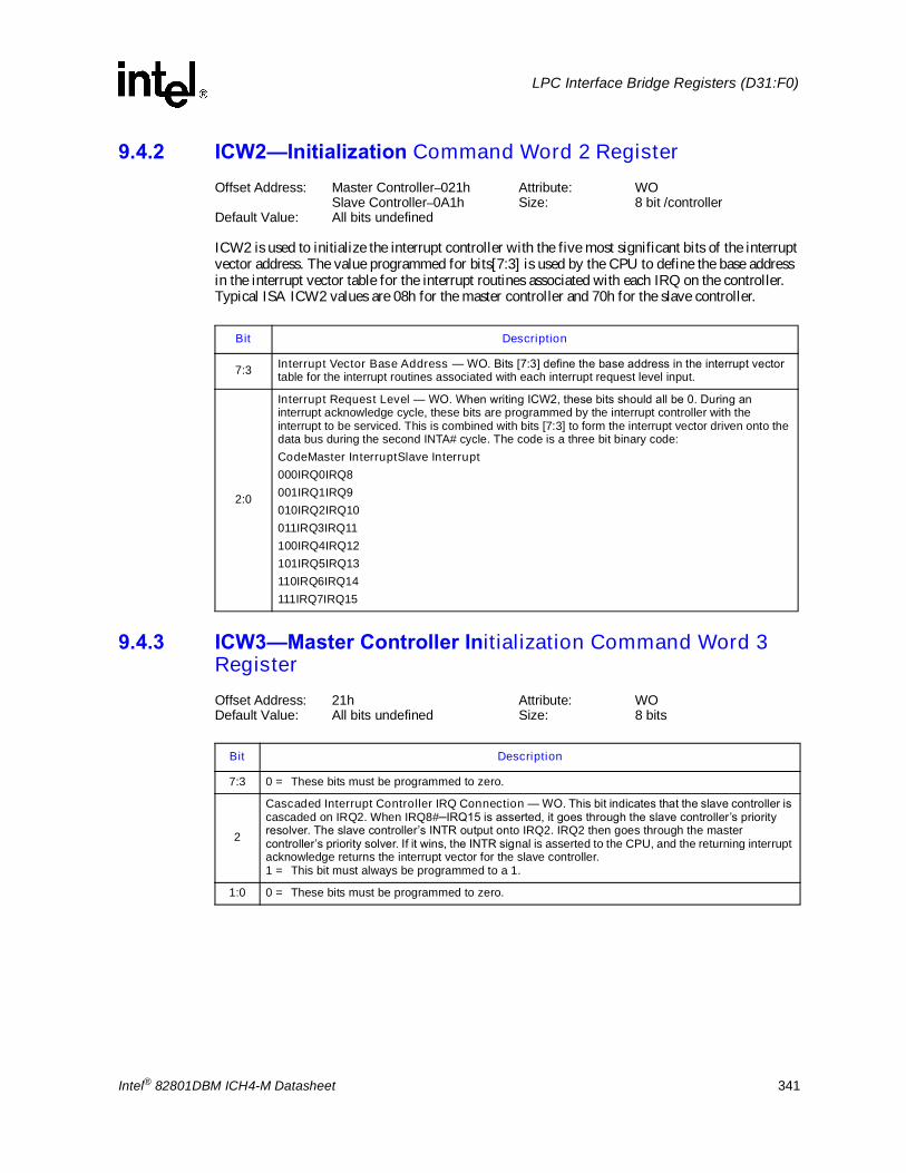
Intel® 82801DBM ICH4-M Datasheet 341
LPC Interface Bridge Registers (D31:F0)
9.4.2 ICW2�Initialization Command Word 2 RegisterOffset Address: Master Controller�021h Attribute: WO Slave Controller�0A1h Size: 8 bit /controllerDefault Value: All bits undefined
ICW2 is used to initialize the interrupt controller with the five most significant bits of the interrupt vector address. The value programmed for bits[7:3] is used by the CPU to define the base address in the interrupt vector table for the interrupt routines associated with each IRQ on the controller. Typical ISA ICW2 values are 08h for the master controller and 70h for the slave controller.
9.4.3 ICW3�Master Controller Initialization Command Word 3 RegisterOffset Address: 21h Attribute: WODefault Value: All bits undefined Size: 8 bits
Bit Description
7:3 Interrupt Vector Base Address � WO. Bits [7:3] define the base address in the interrupt vector table for the interrupt routines associated with each interrupt request level input.
2:0
Interrupt Request Level � WO. When writing ICW2, these bits should all be 0. During an interrupt acknowledge cycle, these bits are programmed by the interrupt controller with the interrupt to be serviced. This is combined with bits [7:3] to form the interrupt vector driven onto the data bus during the second INTA# cycle. The code is a three bit binary code:CodeMaster InterruptSlave Interrupt000IRQ0IRQ8001IRQ1IRQ9010IRQ2IRQ10011IRQ3IRQ11100IRQ4IRQ12101IRQ5IRQ13110IRQ6IRQ14111IRQ7IRQ15
Bit Description
7:3 0 = These bits must be programmed to zero.
2
Cascaded Interrupt Controller IRQ Connection � WO. This bit indicates that the slave controller is cascaded on IRQ2. When IRQ8#�IRQ15 is asserted, it goes through the slave controller�s priority resolver. The slave controller�s INTR output onto IRQ2. IRQ2 then goes through the master controller�s priority solver. If it wins, the INTR signal is asserted to the CPU, and the returning interrupt acknowledge returns the interrupt vector for the slave controller.1 = This bit must always be programmed to a 1.
1:0 0 = These bits must be programmed to zero.

342 Intel® 82801DBM ICH4-M Datasheet
LPC Interface Bridge Registers (D31:F0)
9.4.4 ICW3�Slave Controller Initialization Command Word 3 RegisterOffset Address: A1h Attribute: WODefault Value: All bits undefined Size: 8 bits
9.4.5 ICW4�Initialization Command Word 4 RegisterOffset Address: Master Controller�021h Attribute: WO Slave Controller�0A1h Size: 8 bits
9.4.6 OCW1�Operational Control Word 1 (Interrupt Mask) Register Offset Address: Master Controller�021h Attribute: R/W Slave Controller�0A1h Size: 8 bitsDefault Value: 00h
Bit Description
7:3 0 = These bits must be programmed to zero.
2:0
Slave Identification Code � WO. These bits are compared against the slave identification code broadcast by the master controller from the trailing edge of the first internal INTA# pulse to the trailing edge of the second internal INTA# pulse. These bits must be programmed to 02h to match the code broadcast by the master controller. When 02h is broadcast by the master controller during the INTA# sequence, the slave controller assumes responsibility for broadcasting the interrupt vector.
Bit Description
7:5 0 = These bits must be programmed to zero.
4Special Fully Nested Mode (SFNM) � WO. 0 = Should normally be disabled by writing a 0 to this bit. 1 = Special fully nested mode is programmed.
3Buffered Mode (BUF) � WO.0 = Must be programmed to 0 for the ICH4. This is non-buffered mode.
2Master/Slave in Buffered Mode � WO. Not used.0 = Should always be programmed to 0.
1Automatic End of Interrupt (AEOI) � WO. 0 = This bit should normally be programmed to 0. This is the normal end of interrupt. 1 = Automatic End of Interrupt (AEOI) mode is programmed.
0Microprocessor Mode � WO.1 = Must be programmed to 1 to indicate that the controller is operating in an Intel Architecture-
based system.
Bit Description
7:0Interrupt Request Mask � R/W. When a 1 is written to any bit in this register, the corresponding IRQ line is masked. When a 0 is written to any bit in this register, the corresponding IRQ mask bit is cleared, and interrupt requests will again be accepted by the controller. Masking IRQ2 on the master controller will also mask the interrupt requests from the slave controller.

Intel® 82801DBM ICH4-M Datasheet 343
LPC Interface Bridge Registers (D31:F0)
9.4.7 OCW2�Operational Control Word 2 RegisterOffset Address: Master Controller�020h Attribute: WO Slave Controller�0A0h Size: 8 bitsDefault Value: Bit[4:0]=undefined, Bit[7:5]=001
Following a part reset or ICW initialization, the controller enters the fully nested mode of operation. Non-specific EOI without rotation is the default. Both rotation mode and specific EOI mode are disabled following initialization.
Bit Description
7:5
Rotate and EOI Codes (R, SL, EOI) � WO. These three bits control the Rotate and End of Interrupt modes and combinations of the two.000 = Rotate in Auto EOI Mode (Clear)001 = Non-specific EOI command010 = No Operation011 = Specific EOI Command100 = Rotate in Auto EOI Mode (Set) 101 = Rotate on Non-Specific EOI Command110 = *Set Priority Command111 = *Rotate on Specific EOI Command*L0�L2 Are Used
4:3 OCW2 Select � WO. When selecting OCW2, bits 4:3 = 00
2:0
Interrupt Level Select (L2, L1, L0) � WO. L2, L1, and L0 determine the interrupt level acted upon when the SL bit is active. A simple binary code, outlined below, selects the channel for the command to act upon. When the SL bit is inactive, these bits do not have a defined function; programming L2, L1 and L0 to 0 is sufficient in this case.BitsInterrupt LevelBitsInterrupt Level000IRQ0/8100IRQ4/12001IRQ1/9101IRQ5/13010IRQ2/10110IRQ6/14011IRQ3/11111IRQ7/15

344 Intel® 82801DBM ICH4-M Datasheet
LPC Interface Bridge Registers (D31:F0)
9.4.8 OCW3�Operational Control Word 3 RegisterOffset Address: Master Controller�020h Attribute: WO Slave Controller�0A0h Size: 8 bitsDefault Value: Bit[6,0]=0, Bit[7,4:2]=undefined,
Bit[5,1]=1
Bit Description
7 Reserved. Must be 0.
6Special Mask Mode (SMM) � WO.1 = The Special Mask Mode can be used by an interrupt service routine to dynamically alter the
system priority structure while the routine is executing, through selective enabling/disabling of the other channel's mask bits. Bit 5, the ESMM bit, must be set for this bit to have any meaning.
5Enable Special Mask Mode (ESMM) � WO.0 = Disable. The SMM bit becomes a �don't care�.1 = Enable the SMM bit to set or reset the Special Mask Mode.
4:3 OCW3 Select � WO. When selecting OCW3, bits 4:3 = 01
2
Poll Mode Command � WO.0 = Disable. Poll Command is not issued.1 = Enable. The next I/O read to the interrupt controller is treated as an interrupt acknowledge cycle.
An encoded byte is driven onto the data bus, representing the highest priority level requesting service.
1:0
Register Read Command � WO. These bits provide control for reading the In-Service Register (ISR) and the Interrupt Request Register (IRR). When bit 1=0, bit 0 will not affect the register read selection. When bit 1=1, bit 0 selects the register status returned following an OCW3 read. If bit 0=0, the IRR will be read. If bit 0=1, the ISR will be read. Following ICW initialization, the default OCW3 port address read will be �read IRR�. To retain the current selection (read ISR or read IRR), always write a 0 to bit 1 when programming this register. The selected register can be read repeatedly without reprogramming OCW3. To select a new status register, OCW3 must be reprogrammed prior to attempting the read.00 = No Action01 = No Action10 = Read IRQ Register11 = Read IS Register

Intel® 82801DBM ICH4-M Datasheet 345
LPC Interface Bridge Registers (D31:F0)
9.4.9 ELCR1�Master Controller Edge/Level Triggered Register Offset Address: 4D0h Attribute: R/WDefault Value: 00h Size: 8 bits
In edge mode, (bit[x] = 0), the interrupt is recognized by a low to high transition. In level mode (bit[x] = 1), the interrupt is recognized by a high level. The cascade channel, IRQ2, the heart beat timer (IRQ0), and the keyboard controller (IRQ1), cannot be put into level mode.
Bit Description
7IRQ7 ECL � R/W.0 = Edge.1 = Level.
6IRQ6 ECL � R/W.0 = Edge.1 = Level.
5IRQ5 ECL � R/W.0 = Edge.1 = Level.
4IRQ4 ECL � R/W.0 = Edge.1 = Level.
3IRQ3 ECL � R/W.0 = Edge.1 = Level.
2:0 Reserved. Must be 0.

346 Intel® 82801DBM ICH4-M Datasheet
LPC Interface Bridge Registers (D31:F0)
9.4.10 ELCR2�Slave Controller Edge/Level Triggered Register Offset Address: 4D1h Attribute: R/WDefault Value: 00h Size: 8 bits
In edge mode, (bit[x] = 0), the interrupt is recognized by a low to high transition. In level mode (bit[x] = 1), the interrupt is recognized by a high level. The real time clock, IRQ8#, and the floating point error interrupt, IRQ13, cannot be programmed for level mode.
Bit Description
7IRQ15 ECL � R/W.0 = Edge.1 = Level.
6IRQ14 ECL � R/W.0 = Edge.1 = Level.
5 Reserved. Must be 0.
4IRQ12 ECL � R/W.0 = Edge.1 = Level.
3IRQ11 ECL � R/W.0 = Edge.1 = Level.
2IRQ10 ECL � R/W.0 = Edge.1 = Level.
1IRQ9 ECL � R/W.0 = Edge.1 = Level.
0 Reserved. Must be 0.

Intel® 82801DBM ICH4-M Datasheet 347
LPC Interface Bridge Registers (D31:F0)
9.5 Advanced Interrupt Controller (APIC)
9.5.1 APIC Register MapThe APIC is accessed via an indirect addressing scheme. Two registers are visible by software for manipulation of most of the APIC registers. These registers are mapped into memory space. The registers are shown in Table 9-4.
Table 9-5 lists the registers which can be accessed within the APIC via the Index Register. When accessing these registers, accesses must be done a DWORD at a time. For example, software should never access byte 2 from the Data register before accessing bytes 0 and 1. The hardware will not attempt to recover from a bad programming model in this case.
Table 9-4. APIC Direct Registers
Address Register Name Size Type
FEC0_0000h Index Register 8 bits R/W
FEC0_0010h Data Register 32 bits R/W
FECO_0020h IRQ Pin Assertion Register 8 bits WO
FECO_0040h EOI Register 8 bits WO
Table 9-5. APIC Indirect Registers
Index Register Name Size Type
00h ID 32 bits R/W
01h Version 32 bits RO
02h Arbitration ID 32 bits RO
03h Boot Configuration 32 bits R/W
03�0Fh Reserved RO
10�11h Redirection Table 0 64 bits R/W, RO
12�13h Redirection Table 1 64 bits R/W, RO
... ... ... ...
3E�3Fh Redirection Table 23 64 bits R/W, RO
40�FFh Reserved RO

348 Intel® 82801DBM ICH4-M Datasheet
LPC Interface Bridge Registers (D31:F0)
9.5.2 IND�Index RegisterMemory Address FEC0_0000h Attribute: R/WDefault Value: 00h Size: 8 bits
The Index Register will select which APIC indirect register to be manipulated by software. The selector values for the indirect registers are listed in Table 9-5. Software will program this register to select the desired APIC internal register
.
9.5.3 DAT�Data RegisterMemory Address FEC0_0010h Attribute: R/WDefault Value: 00000000h Size: 32 bits
This is a 32-bit register specifying the data to be read or written to the register pointed to by the Index register. This register can only be accessed in DWORD quantities.
9.5.4 IRQPA�IRQ Pin Assertion RegisterMemory Address FEC0_0020h Attribute: WODefault Value: N/A Size: 32 bits
The IRQ Pin Assertion Register is present to provide a mechanism to scale the number of interrupt inputs into the I/O APIC without increasing the number of dedicated input pins. When a device that supports this interrupt assertion protocol requires interrupt service, that device will issue a write to this register. Bits 4:0 written to this register contain the IRQ number for this interrupt. The only valid values are 0�23. Bits 31:5 are ignored. To provide for future expansion, peripherals should always write a value of 0 for Bits 31:5.
See Section 5.8.4 for more details on how PCI devices will use this field.
Note: Writes to this register are only allowed by the processor and by masters on the ICH4�s PCI bus. Writes by devices on PCI buses above the ICH4 (e.g., a PCI segment on a P64H) are not supported.
Bit Description
7:0 APIC Index � R/W. This is an 8-bit pointer into the I/O APIC register table.
Bit Description
7:0 APIC Data � R/W. This is a 32-bit register for the data to be read or written to the APIC indirect register pointed to by the Index register.
Bit Description
31:5 Reserved. To provide for future expansion, the CPU should always write a value of 0 to Bits 31:5.
4:0 IRQ Number � WO. Bits 4:0 written to this register contain the IRQ number for this interrupt. The only valid values are 0�23.

Intel® 82801DBM ICH4-M Datasheet 349
LPC Interface Bridge Registers (D31:F0)
9.5.5 EOIR�EOI RegisterMemory Address FEC0_0040h Attribute: WODefault Value: N/A Size: 32 bits
The EOI register is present to provide a mechanism to maintain the level triggered semantics for level-triggered interrupts issued on the parallel bus.
When a write is issued to this register, the I/O APIC will check the lower 8 bits written to this register, and compare it with the vector field for each entry in the I/O Redirection Table. When a match is found, the Remote_IRR bit for that I/O Redirection Entry will be cleared.
Note: This is similar to what already occurs when the APIC sees the EIO message on the serial bus. Note that if multiple I/O Redirection entries, for any reason, assign the same vector for more than one interrupt input, each of those entries will have the Remote_IRR bit reset to 0. The interrupt which was prematurely reset will not be lost because if its input remained active when the Remote_IRR bit is cleared, the interrupt will be reissued and serviced at a later time. Note: Only bits 7:0 are actually used. Bits 31:8 are ignored by the ICH4.
Note: To provide for future expansion, the CPU should always write a value of 0 to Bits 31:8.
9.5.6 ID�Identification RegisterIndex Offset: 00h Attribute: R/WDefault Value: 00000000h Size: 32 bits
The APIC ID serves as a physical name of the APIC. The APIC bus arbitration ID for the APIC is derived from its I/O APIC ID. This register is reset to zero on power up reset
Bit Description
31:8 Reserved. To provide for future expansion, the processor should always write a value of 0 to Bits 31:8.
7:0Redirection Entry Clear � WO. When a write is issued to this register, the I/O APIC will check this field, and compare it with the vector field for each entry in the I/O Redirection Table. When a match is found, the Remote_IRR bit for that I/O Redirection Entry will be cleared.
Bit Description
31:28 Reserved
27:24 APIC ID � R/W. Software must program this value before using the APIC.
23:16 Reserved
15 Scratchpad bit.
14:0 Reserved

350 Intel® 82801DBM ICH4-M Datasheet
LPC Interface Bridge Registers (D31:F0)
9.5.7 VER�Version RegisterIndex Offset: 01h Attribute: RODefault Value: 00170002h Size: 32 bits
Each I/O APIC contains a hardwired Version Register that identifies different implementation of APIC and their versions. The maximum redirection entry information also is in this register, to let software know how many interrupt are supported by this APIC.
9.5.8 ARBID�Arbitration ID RegisterIndex Offset: 02h Attribute: RODefault Value: 00000000h Size: 32 bits
This register contains the bus arbitration priority for the APIC. If APIC Clock is running, this register is loaded whenever the APIC ID register is loaded. A rotating priority scheme is used for APIC bus arbitration. The winner of the arbitration becomes the lowest priority agent and assumes an arbitration ID of 0.
a
9.5.9 BOOT_CONFIG�Boot Configuration RegisterIndex Offset: 03h Attribute: R/WDefault Value: 00000000h Size: 32 bits
This register is used to control the interrupt delivery mechanism for the APIC.a
Bit Description
31:24 Reserved
23:16Maximum Redirection Entries � RO. This is the entry number (0 being the lowest entry) of the highest entry in the redirection table. It is equal to the number of interrupt input pins minus one and is in the range 0 through 239. In the ICH4 this field is hardwired to 17h to indicate 24 interrupts.
15 PRQ � RO. This bit is set to 1 to indicate that this version of the I/O APIC implements the IRQ Assertion register and allows PCI devices to write to it to cause interrupts.
14:8 Reserved
7:0 Version � RO. This is a version number that identifies the implementation version.
Bit Description
31:28 Reserved
27:24 I/O APIC Identification � RO. This 4-bit field contains the I/O APIC Arbitration ID.
23:0 Reserved
Bit Description
31:1 Reserved
0Delivery Type (DT) � R/W.0 = Interrupt delivery mechanism is via the APIC serial bus (default).1 = Interrupt delivery mechanism is a Processor System Bus message.

Intel® 82801DBM ICH4-M Datasheet 351
LPC Interface Bridge Registers (D31:F0)
9.5.10 Redirection TableIndex Offset: 10h�11h (vector 0) through Attribute: R/W, RO
3E�3Fh (vector 23)Default Value: Bit 16=1, Bits[15:12]=0. Size: 64 bits each, (accessed as
All other bits undefined two 32 bit quantities)
The Redirection Table has a dedicated entry for each interrupt input pin. The information in the Redirection Table is used to translate the interrupt manifestation on the corresponding interrupt pin into an APIC message.
The APIC will respond to an edge triggered interrupt as long as the interrupt is held until after the acknowledge cycle has begun. Once the interrupt is detected, a delivery status bit internally to the I/O APIC is set. The state machine will step ahead and wait for an acknowledgment from the APIC bus unit that the interrupt message was sent over the APIC bus. Only then will the I/O APIC be able to recognize a new edge on that interrupt pin. That new edge will only result in a new invocation of the handler if its acceptance by the destination APIC causes the Interrupt Request Register bit to go from 0 to 1. (In other words, if the interrupt was not already pending at the destination.)
Bit Description
63:56
Destination � R/W. If bit 11 of this entry is 0 [Physical], then bits [59:56] specifies an APIC ID. In this case, bits 63:59 should be programmed by software to 0. If bit 11 of this entry is 1 [Logical], then bits [63:56] specify the logical destination address of a set of processors.
55:48 Extended Destination ID (EDID). These bits are only sent to a local APIC when in Processor System Bus mode. They become bits [11:4] of the address.
47:17 Reserved
16
Mask � R/W.0 = Not masked: An edge or level on this interrupt pin results in the delivery of the interrupt to the
destination.1 = Masked: Interrupts are not delivered nor held pending. Setting this bit after the interrupt is
accepted by a local APIC has no effect on that interrupt. This behavior is identical to the device withdrawing the interrupt before it is posted to the processor. It is software's responsibility to deal with the case where the mask bit is set after the interrupt message has been accepted by a local APIC unit but before the interrupt is dispensed to the processor.
15
Trigger Mode � R/W. This field indicates the type of signal on the interrupt pin that triggers an interrupt.0 = Edge triggered.1 = Level triggered.
14
Remote IRR � R/W. This bit is used for level-triggered interrupts; its meaning is undefined for edge-triggered interrupts. 0 = Reset when an EOI message is received from a local APIC.1 = Set when Local APIC/s accept the level interrupt sent by the I/O APIC.
13
Interrupt Input Pin Polarity � R/W. This bit specifies the polarity of each interrupt signal connected to the interrupt pins.0 = Active high.1 = Active low.
12
Delivery Status � RO. This field contains the current status of the delivery of this interrupt. Writes to this bit have no effect.0 = Idle. No activity for this interrupt.1 = Pending. Interrupt has been injected, but delivery is held up due to the APIC bus being busy
or the inability of the receiving APIC unit to accept the interrupt at this time.
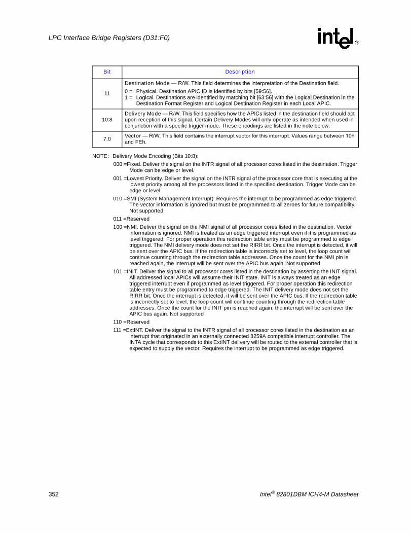
352 Intel® 82801DBM ICH4-M Datasheet
LPC Interface Bridge Registers (D31:F0)
NOTE: Delivery Mode Encoding (Bits 10:8): 000 =Fixed. Deliver the signal on the INTR signal of all processor cores listed in the destination. Trigger
Mode can be edge or level.001 =Lowest Priority. Deliver the signal on the INTR signal of the processor core that is executing at the
lowest priority among all the processors listed in the specified destination. Trigger Mode can be edge or level.
010 =SMI (System Management Interrupt). Requires the interrupt to be programmed as edge triggered. The vector information is ignored but must be programmed to all zeroes for future compatibility. Not supported
011 =Reserved100 =NMI. Deliver the signal on the NMI signal of all processor cores listed in the destination. Vector
information is ignored. NMI is treated as an edge triggered interrupt even if it is programmed as level triggered. For proper operation this redirection table entry must be programmed to edge triggered. The NMI delivery mode does not set the RIRR bit. Once the interrupt is detected, it will be sent over the APIC bus. If the redirection table is incorrectly set to level, the loop count will continue counting through the redirection table addresses. Once the count for the NMI pin is reached again, the interrupt will be sent over the APIC bus again. Not supported
101 =INIT. Deliver the signal to all processor cores listed in the destination by asserting the INIT signal. All addressed local APICs will assume their INIT state. INIT is always treated as an edge triggered interrupt even if programmed as level triggered. For proper operation this redirection table entry must be programmed to edge triggered. The INIT delivery mode does not set the RIRR bit. Once the interrupt is detected, it will be sent over the APIC bus. If the redirection table is incorrectly set to level, the loop count will continue counting through the redirection table addresses. Once the count for the INIT pin is reached again, the interrupt will be sent over the APIC bus again. Not supported
110 =Reserved111 =ExtINT. Deliver the signal to the INTR signal of all processor cores listed in the destination as an
interrupt that originated in an externally connected 8259A compatible interrupt controller. The INTA cycle that corresponds to this ExtINT delivery will be routed to the external controller that is expected to supply the vector. Requires the interrupt to be programmed as edge triggered.
11
Destination Mode � R/W. This field determines the interpretation of the Destination field.0 = Physical. Destination APIC ID is identified by bits [59:56].1 = Logical. Destinations are identified by matching bit [63:56] with the Logical Destination in the
Destination Format Register and Logical Destination Register in each Local APIC.
10:8Delivery Mode � R/W. This field specifies how the APICs listed in the destination field should act upon reception of this signal. Certain Delivery Modes will only operate as intended when used in conjunction with a specific trigger mode. These encodings are listed in the note below:
7:0 Vector � R/W. This field contains the interrupt vector for this interrupt. Values range between 10h and FEh.
Bit Description

Intel® 82801DBM ICH4-M Datasheet 353
LPC Interface Bridge Registers (D31:F0)
9.6 Real Time Clock Registers
9.6.1 I/O Register Address MapThe RTC internal registers and RAM are organized as two banks of 128 bytes each, called the standard and extended banks. The first 14 bytes of the standard bank contain the RTC time and date information along with four registers, A�D, that are used for configuration of the RTC. The extended bank contains a full 128 bytes of battery backed SRAM, and will be accessible even when the RTC module is disabled (via the RTC configuration register). Registers A�D do not physically exist in the RAM.
All data movement between the host processor and the real-time clock is done through registers mapped to the standard I/O space. The register map appears in Table 9-6.
NOTES:1. I/O locations 70h and 71h are the standard ISA location for the real-time clock. The map for this bank is
shown in Table 9-7. Locations 72h and 73h are for accessing the extended RAM. The extended RAM bank is also accessed using an indexed scheme. I/O address 72h is used as the address pointer and I/O address 73h is used as the data register. Index addresses above 127h are not valid. If the extended RAM is not needed, it may be disabled.
2. Software must preserve the value of bit 7 at I/O addresses 70h and 74h. When writing to these addresses, software must first read the value, and then write the same value for bit 7 during the sequential address write.
3. Accesses to 70h, 72h, 74h, and 76h do affect the NMI mask (bit 7 of 70h).
Table 9-6. RTC I/O Registers
I/O Locations If U128E bit = 0 Function
70h and 74h Also alias to 72h and 76h Real-Time Clock (Standard RAM) Index Register
71h and 75h Also alias to 73h and 77h Real-Time Clock (Standard RAM) Target Register
72h and 76h Extended RAM Index Register (if enabled)
73h and 77h Extended RAM Target Register (if enabled)

354 Intel® 82801DBM ICH4-M Datasheet
LPC Interface Bridge Registers (D31:F0)
9.6.2 Indexed RegistersThe RTC contains two sets of indexed registers that are accessed using the two separate Index and Target registers (70/71h or 72/73h), as shown in Table 9-7.
Table 9-7. RTC (Standard) RAM Bank
Index Name
00h Seconds
01h Seconds Alarm.
02h Minutes
03h Minutes Alarm
04h Hours
05h Hours Alarm
06h Day of Week
07h Day of Month
08h Month
09h Year
0Ah Register A
0Bh Register B
0Ch Register C
0Dh Register D
0Eh�7Fh 114 Bytes of User RAM

Intel® 82801DBM ICH4-M Datasheet 355
LPC Interface Bridge Registers (D31:F0)
9.6.2.1 RTC_REGA�Register ARTC Index: 0A Attribute: R/WDefault Value: Undefined Size: 8 bitLockable: No Power Well: RTC
This register is used for general configuration of the RTC functions. None of the bits are affected by RSMRST# or any other ICH4 reset signal.
Bit Description
7
Update In Progress (UIP) � R/W. This bit may be monitored as a status flag. 0 = The update cycle will not start for at least 492 µs. The time, calendar, and alarm information in
RAM is always available when the UIP bit is 0.1 = The update is soon to occur or is in progress.
6:4
Division Chain Select (DV[2:0]) � R/W. These three bits control the divider chain for the oscillator, and are not affected by RSMRST# or any other reset signal. DV[2] corresponds to bit 6.010 = Normal Operation11X = Divider Reset101 = Bypass 15 stages (test mode only)100 = Bypass 10 stages (test mode only)011 = Bypass 5 stages (test mode only)001 = Invalid000 = Invalid
3:0
Rate Select (RS[3:0]) � R/W. Selects one of 13 taps of the 15 stage divider chain. The selected tap can generate a periodic interrupt if the PIE bit is set in Register B. Otherwise this tap will set the PF flag of Register C. If the periodic interrupt is not to be used, these bits should all be set to zero. RS3 corresponds to bit 3.0000 = Interrupt never toggles0001 = 3.90625 ms0010 = 7.8125 ms0011 = 122.070 µs0100 = 244.141 µs0101 = 488.281 µs0110 = 976.5625 µs0111 = 1.953125 ms1000 = 3.90625 ms1001 = 7.8125 ms1010 = 15.625 ms1011 = 31.25 ms1100 = 62.5 ms1101 = 125 ms1110 = 250 ms1111= 500 ms

356 Intel® 82801DBM ICH4-M Datasheet
LPC Interface Bridge Registers (D31:F0)
9.6.2.2 RTC_REGB�Register B (General Configuration)RTC Index: 0Bh Attribute: R/WDefault Value: U0U00UUU (U: Undefined) Size: 8 bitLockable: No Power Well: RTC
Bit Description
7
Update Cycle Inhibit (SET) � R/W. Enables/Inhibits the update cycles. This bit is not affected by RSMRST# nor any other reset signal.0 = Update cycle occurs normally once each second.1 = A current update cycle will abort and subsequent update cycles will not occur until SET is
returned to zero. When set is one, the BIOS may initialize time and calendar bytes safely.
NOTE: This bit should be set then cleared by BIOS early in BIOS POST, after each power-up directly after coin-cell batter insertion.
6Periodic Interrupt Enable (PIE) � R/W. This bit is cleared by RSMRST#, but not on any other reset.0 = Disable. 1 = Allows an interrupt to occur with a time base set with the RS bits of register A.
5
Alarm Interrupt Enable (AIE) � R/W. This bit is cleared by RSMRST#, but not on any other reset. 0 = Disable.1 = Allows an interrupt to occur when the AF is set by an alarm match from the update cycle. An
alarm can occur once a second, one an hour, once a day, or one a month.
4
Update-Ended Interrupt Enable (UIE) � R/W. This bit is cleared by RSMRST#, but not on any other reset.0 = Disable.1 = Allows an interrupt to occur when the update cycle ends.
3Square Wave Enable (SQWE) � R/W. This bit serves no function in the ICH4. It is left in this register bank to provide compatibility with the Motorola* 146818B. The ICH4 has no SQW pin. This bit is cleared by RSMRST#, but not on any other reset.
2
Data Mode (DM) � R/W. Specifies either binary or BCD data representation. This bit is not affected by RSMRST# nor any other reset signal.0 = BCD1 = Binary
1
Hour Format (HOURFORM) � R/W. Indicates the hour byte format. This bit is not affected by RSMRST# nor any other reset signal.0 = Twelve-hour mode. In twelve-hour mode, the seventh bit represents AM as zero and PM as one.1 = Twenty-four hour mode.
0
Daylight Savings Enable (DSE) � R/W. Triggers two special hour updates per year. The days for the hour adjustment are those specified in United States federal law as of 1987, which is different than previous years. This bit is not affected by RSMRST# nor any other reset signal. 0 = Daylight Savings Time updates do not occur.1 = a) Update on the first Sunday in April, where time increments from 1:59:59 AM to 3:00:00 AM.
b) Update on the last Sunday in October when the time first reaches 1:59:59 AM, it is changed to 1:00:00 AM. The time must increment normally for at least two update cycles (seconds) previous to these conditions for the time change to occur properly.

Intel® 82801DBM ICH4-M Datasheet 357
LPC Interface Bridge Registers (D31:F0)
9.6.2.3 RTC_REGC�Register C (Flag Register)RTC Index: 0Ch Attribute: RODefault Value: 00U00000 (U: Undefined) Size: 8 bitLockable: No Power Well: RTC
Writes to Register C have no effect.
9.6.2.4 RTC_REGD�Register D (Flag Register)RTC Index: 0Dh Attribute: R/WDefault Value: 10UUUUUU (U: Undefined) Size: 8 bitLockable: No Power Well: RTC
Bit Description
7 Interrupt Request Flag (IRQF) � RO. IRQF = (PF * PIE) + (AF * AIE) + (UF *UFE). This also causes the CH_IRQ_B signal to be asserted. This bit is cleared upon RSMRST# or a read of Register C.
6Periodic Interrupt Flag (PF) � RO. This bit is cleared upon RSMRST# or a read of Register C.0 = If no taps are specified via the RS bits in Register A, this flag will not be set.1 = Periodic interrupt Flag will be 1 whenever the tap specified by the RS bits of register A is 1.
5Alarm Flag (AF) � RO.0 = This bit is cleared upon RTCRST# or a read of Register C.1 = Alarm Flag will be set after all Alarm values match the current time.
4Update-ended Flag (UF) � RO. 0 = The bit is cleared upon RSMRST# or a read of Register C.1 = Set immediately following an update cycle for each second.
3:0 Reserved. Will always report 0.
Bit Description
7Valid RAM and Time Bit (VRT) � R/W.0 = This bit should always be written as a 0 for write cycle; however, it will return a 1 for read cycles.1 = This bit is hardwired to 1 in the RTC power well.
6 Reserved. This bit always returns a 0 and should be set to 0 for write cycles.
5:0Date Alarm � R/W. These bits store the date of month alarm value. If set to 000000b, then a don�t care state is assumed. The host must configure the date alarm for these bits to do anything, yet they can be written at any time. If the date alarm is not enabled, these bits will return zeros to mimic the functionality of the Motorola 146818B. These bits are not affected by RESET.

358 Intel® 82801DBM ICH4-M Datasheet
LPC Interface Bridge Registers (D31:F0)
9.7 Processor Interface Registers
9.7.1 NMI_SC�NMI Status and Control RegisterI/O Address: 61h Attribute: R/W, RODefault Value: 00h Size: 8 bitLockable: No Power Well: Core
Bit Description
7
SERR# NMI Source Status (SERR#_NMI_STS) � RO.1 = PCI agent detected a system error and pulses the PCI SERR# line. This interrupt source is
enabled by setting bit 2 to 0. To reset the interrupt, set bit 2 to 1 and then set it to 0. When writing to port 61h, this bit must be 0.
6
IOCHK# NMI Source Status (IOCHK_NMI_STS) � RO. 1 = An ISA agent (via SERIRQ) asserted IOCHK# on the ISA bus. This interrupt source is enabled
by setting bit 3 to 0. To reset the interrupt, set bit 3 to 0 and then set it to 1. When writing to port 61h, this bit must be a 0.
5Timer Counter 2 OUT Status (TMR2_OUT_STS) � RO. This bit reflects the current state of the 8254 counter 2 output. Counter 2 must be programmed following any PCI reset for this bit to have a determinate value. When writing to port 61h, this bit must be a 0.
4Refresh Cycle Toggle (REF_TOGGLE) � RO. This signal toggles from either 0 to 1 or 1 to 0 at a rate that is equivalent to when refresh cycles would occur. When writing to port 61h, this bit must be a 0.
3IOCHK# NMI Enable (IOCHK_NMI_EN) � R/W.0 = Enabled.1 = Disabled and cleared.
2PCI SERR# Enable (PCI_SERR_EN) � R/W. 0 = SERR# NMIs are enabled.1 = SERR# NMIs are disabled and cleared.
1Speaker Data Enable (SPKR_DAT_EN) � R/W. 0 = SPKR output is a 0.1 = SPKR output is equivalent to the Counter 2 OUT signal value.
0Timer Counter 2 Enable (TIM_CNT2_EN) � R/W. 0 = Disable1 = Enable

Intel® 82801DBM ICH4-M Datasheet 359
LPC Interface Bridge Registers (D31:F0)
9.7.2 NMI_EN�NMI Enable (and Real Time Clock Index) RegisterI/O Address: 70h Attribute: R/W-SpecialDefault Value: 80h Size: 8 bitLockable: No Power Well: Core
Note: The RTC Index field is write-only for normal operation. This field can only be read in Alt-Access Mode. Note, however, that this register is aliased to Port 74h (documented in Table 17-2), and all bits are readable at that address.
9.7.3 PORT92�Fast A20 and Init RegisterI/O Address: 92h Attribute: R/WDefault Value: 00h Size: 8 bitLockable: No Power Well: Core
9.7.4 COPROC_ERR�Coprocessor Error RegisterI/O Address: F0h Attribute: WODefault Value: 00h Size: 8 bitsLockable: No Power Well: Core
Bits Description
7NMI Enable (NMI_EN) � R/W.0 = Enable NMI sources.1 = Disable All NMI sources.
6:0 Real Time Clock Index Address (RTC_INDX) � R/W. This data goes to the RTC to select which register or CMOS RAM address is being accessed.
Bit Description
7:2 Reserved
1
Alternate A20 Gate (ALT_A20_GATE) � R/W. This bit is Or�d with the A20GATE input signal to generate A20M# to the processor.0 = A20M# signal can potentially go active.1 = This bit is set when INIT# goes active.
0 INIT_NOW � R/W. When this bit transitions from a 0 to a 1, the ICH4 will force INIT# active for 16 PCI clocks.
Bits Description
7:0COPROC_ERR � WO. Any value written to this register will cause IGNNE# to go active, if FERR# had generated an internal IRQ13. For FERR# to generate an internal IRQ13, the COPROC_ERR_EN bit (Device 31:Function 0, Offset D0, Bit 13) must be 1.

360 Intel® 82801DBM ICH4-M Datasheet
LPC Interface Bridge Registers (D31:F0)
9.7.5 RST_CNT�Reset Control RegisterI/O Address: CF9h Attribute: R/WDefault Value: 00h Size: 8 bitLockable: No Power Well: Core
Bit Description
7:4 Reserved
3
Full Reset (FULL_RST) � R/W. This bit is used to determine the states of SLP_S3#, SLP_S4# and SLP_S5# after a CF9 hard reset (SYS_RST =1 and RST_CPU is set to 1), after PWROK going low (with RSMRST# high), or after two TCO timeouts.0 = ICH4 will keep SLP_S3#, SLP_S4# and SLP_S5# high.1 = ICH4 will drive SLP_S3#, SLP_S4# and SLP_S5# low for 3�5 seconds.
2 Reset CPU (RST_CPU) � R/W. When this bit transitions from a 0 to a 1, it initiates a hard or soft reset, as determined by the SYS_RST bit (bit 1 of this register).
1
System Reset (SYS_RST) � R/W. This bit is used to determine a hard or soft reset to the processor.0 = When RST_CPU bit goes from 0 to 1, the ICH4 performs a soft reset by activating INIT# for
16 PCI clocks.1 = When RST_CPU bit goes from 0 to 1, the ICH4 performs a hard reset by activating PCIRST#
for 1 millisecond. It also resets the resume well bits (except for those noted throughout the EDS). The SLP_S3#, SLP_S4#, and SLP_S5# signals will not go active.
0 Reserved

Intel® 82801DBM ICH4-M Datasheet 361
LPC Interface Bridge Registers (D31:F0)
9.8 Power Management Registers (D31:F0)The power management registers are distributed within the PCI Device 31: Function 0 space, as well as a separate I/O range. Each register is described below. Unless otherwise indicate, bits are in the main (core) power well.
Bits not explicitly defined in each register are assumed to be reserved. When writing to a reserved bit, the value should always be 0. Software should not attempt to use the value read from a reserved bit, as it may not be consistently 1 or 0.
9.8.1 Power Management PCI Configuration Registers (D31:F0)Table 9-8 shows a small part of the configuration space for PCI Device 31: Function 0. It includes only those registers dedicated for power management. Some of the registers are only used for Legacy Power management schemes.
Table 9-8. PCI Configuration Map (PM�D31:F0)
Offset Mnemonic Register Name Default Type
40h�43h PM_BASE ACPI Base Address (See Section 9.1.10) 00000001h R/W
44h ACPI_CNTL ACPI Control (See Section 9.1.11) 00h R/W
A0h GEN_PMCON_1 General Power Management Configuration 1 0000h R/W, RO,
R/WO, R/WC
A2h GEN_PMCON_2 General Power Management Configuration 2 0000h R/WC, R/W
A4h GEN_PMCON_3 General Power Management Configuration 3 00h R/W, R/WC
A8h STPCLK_DEL Stop Clock Delay Register 0Dh R/W
B8�BBh GPI_ROUT GPI Route Control 00000000h R/W
C0 TRP_FWD_EN I/O Monitor Trap Forwarding Enable
C4�CAhh MON[n]_TRP_RNG I/O Monitor[4:7] Trap Range 0000h R/W
CCh MON_TRP_MSK I/O Monitor Trap Range Mask 0000h R/W

362 Intel® 82801DBM ICH4-M Datasheet
LPC Interface Bridge Registers (D31:F0)
9.8.1.1 GEN_PMCON_1�General PM Configuration 1 Register (PM�D31:F0)Offset Address: A0h Attribute: R/W, RO, R/WO, R/WCDefault Value: 00h Size: 16 bitLockable: No Usage: ACPI, Legacy
Power Well: Core
Bit Description
15:12Global Standby Timer Timeout Count (GST_TIMEOUT) � R/W. This field sets the number of clock ticks that the Global Standby Timer will count before generating a wake event. The GST starts counting when the ICH4 enters the S1-M state. If a value of 0h is entered into this field the GST will not count, and no wake event will be generated. The GST_TICK bit sets the tick rate.
11
Global Standby Timer Tick Rate (GST_TICK) � R/W.0 = Counts by 65.536 seconds (1.0921 minute). This yields a GST timeout range of 1 to 17.476 1 = Counts by 2097.152 seconds (34.952 minutes). This yields a GST timeout range of
0.58 hours to 8 hours 45 minutes 22.816 seconds.
10 Reserved
9PWRBTN_LVL � RO. This read-only bit indicates the current state of the PWRBTN# signal. 0 = Low.1 = High.
8 Deeper Sleep in S1-M state (DPRSLP_S1) � R/W. If this bit is set, then when entering the S1-M state, the ICH4 will use the C4 sequence (rather than the standard sequence).
7 Enter C4 When C3 Invoked (C4onC3_EN). If this bit is set, then when software does a LVL3 read, the ICH4 will transition to the C4 state.
6 64_EN. Software sets this bit to indicate that the processor is an IA_64 processor, not an IA_32 processor.This may be used in various state machines where there are behavioral differences.
5
CPU SLP# Enable (CPUSLP_EN) � R/W. 0 = Disable.1 = Enables the CPUSLP# signal to go active in the C3 and C4 states. This reduces the CPU
power.Note that CPUSLP# will go active during Intel® SpeedStep� technology transitions and on entry to S1-M, S3, S4 and S5 even if this bit is not set.
4SMI_LOCK � R/W-Once. When this bit is set, writes to the GLB_SMI_EN bit will have no effect. Once the SMI_LOCK bit is set, writes of 0 to SMI_LOCK bit will have no effect (i.e., once set, this bit can only be cleared by PCIRST#).
3
Intel SpeedStep Enable (SS_EN) � R/W. 0 = Intel SpeedStep technology logic is disabled and the SS_CNT and SS_CNFregister will not
be visible (reads to SS_CNT will return 00h and writes will have no effect).1 = Intel SpeedStep technology logic is enabled.
2
PCI CLKRUN# Enable (CLKRUN_EN) � R/W.0 = Disable. ICH4 will drive the CLKRUN# signal low.1 = Enable CLKRUN# logic to control the system PCI clock via the CLKRUN# and STP_PCI#
signals.Note that when the SLP_EN# bit is set, the ICH4 will drive the CLKRUN# signal low regardless of the state of the CLKRUN_EN bit. This ensures that the PCI and LPC clocks will continue running during a transition to a sleep state.
1:0
Periodic SMI# Rate Select (PER_SMI_SEL) � R/W. Set by software to control the rate the periodic SMI# is generated.00 = 1 minute01 = 32 seconds10 = 16 seconds11 = 8 seconds

Intel® 82801DBM ICH4-M Datasheet 363
LPC Interface Bridge Registers (D31:F0)
9.8.1.2 GEN_PMCON_2�General PM Configuration 2 Register (PM�D31:F0)Offset Address: A2h Attribute: R/WC, R/WDefault Value: 00h Size: 8 bitLockable: No Usage: ACPI, Legacy
Power Well: Resume
NOTE: VRMPWROK/VGATE is sampled using the RTC clock. Therefore, low times that are less than one RTC clock period may not be detected by the ICH4.
Bit Description
7 Reserved
6:5
CPU PLL Lock Time (CPLT) � R/W. This field indicates the amount of time that the processor needs to lock its PLLs. This is used where timing t208 applies (see Chapter 17). 00 = Minimum lock time of 30.7 µs (Default)01 = min 61.4 µs, 10 = min 122.8 µs, and 11 = min 245.6 µs. It is the responsibility of the BIOS to program the correct value in this field prior to the first transition to C3 or C4 states (or performing Intel SpeedStep Technology transitions).
4System Reset Status (SRS)� R/WC. ICH4 sets this bit when the SYS_RESET# button is pressed. BIOS is expected to read this bit and clear it if it is set. This bit is also reset by RSMRST# and CF9h resets.
3
CPU Thermal Trip Status (CTS)� R/WC. This bit is set when PCIRST# is inactive and CPUTHRMTRIP# goes active while the system is in an S0 or S1-M state. This bit is also reset by RSMRST# and CF9h resets. It is not reset by the shutdown and reboot associated with the CPUTHRMTRIP# event.
2 Reserved
1
CPU Power Failure (CPUPWR_FLR) � R/WC.0 = Software clears this bit by writing a 0 to the bit position.1 = Indicates that the VGATE signal from the processor�s VRM went low. This bit will not be set if
VGATE went low due to an Intel® SpeedStep� technology transition, during C4 entry/exit, or S1-M entry/exit (if DPSLP# is enabled).
0
PWROK Failure (PWROK_FLR) � R/WC.0 = Software clears this bit by writing a 1 to the bit position, or when the system goes into a G3
state.1 = This bit will be set any time PWROK goes low, when the system was in S0, or S1-M state. The
bit will be cleared only by software by writing a 1 to this bit or when the system goes to a G3 state.
NOTES:1. Traditional designs have a reset button logically AND�d with the PWROK signal from the power
supply and the CPU�s voltage regulator module. If this is done with the ICH4, the PWROK_FLR bit will be set. The ICH4 treats this internally as if the RSMRST# signal had gone active. However, it is not treated as a full power failure. If PWROK goes inactive and then active (but RSMRST# stays high), then the ICH4 will reboot (regardless of the state of the AFTERG3 bit). If the RSMRST# signal also goes low before PWROK goes high, then this is a full power failure, and the reboot policy is controlled by the AFTERG3 bit.
2. In the case of true PWROK failure, PWROK will go low first before the VRMPWRGD/VGATE.

364 Intel® 82801DBM ICH4-M Datasheet
LPC Interface Bridge Registers (D31:F0)
9.8.1.3 GEN_PMCON_3�General PM Configuration 3 Register (PM�D31:F0)Offset Address: A4h Attribute: R/W, R/WCDefault Value: 00h Size: 8 bitLockable: No Usage: ACPI, Legacy
Power Well: RTC
NOTE: RSMRST# is sampled using the RTC clock. Therefore, low times that are less than one RTC clock period may not be detected by the ICH4.
Bit Description
7:6
SWSMI_RATE_SEL � R/W. This 2-bit value indicates when the SWSMI timer will time out. Valid values are:
00 = 1.5 ms ± 0.5 ms
01 = 16 ms ± 4 ms
10 = 32 ms ± 4 ms11 = 64 ms ± 4 ms
5:3 Reserved
2
RTC Power Status (RTC_PWR_STS) � R/W. This bit is set when RTCRST# is low. The bit is not cleared by any type of reset. When the system boots, BIOS can detect that the FREQ_STRAP register contents are 1111 (the default when RTCRST# has been low). If this bit is also set, then BIOS knows the RTC battery had been removed. In that case, BIOS should take steps to reprogram the FREQ_STRAP register with the correct value, and then reboot the system.
1
Power Failure (PWR_FLR) � R/WC. This bit is in the RTC well, and is not cleared by any type of reset except RTCRST#.0 = Indicates that the trickle current has not failed since the last time the bit was cleared. Software
clears this bit by writing a 1 to the bit position.1 = Indicates that the trickle current (from the main battery or trickle supply) was removed or failed.
NOTE: Clearing CMOS in an ICH4-based platform can be done by using a jumper on RTCRST# or GPI, or using SAFEMODE strap. Implementations should not attempt to clear CMOS by using a jumper to pull VccRTC low.
0
AFTERG3_EN � R/W. Determines what state to go to when power is re-applied after a power failure (G3 state). This bit is in the RTC well and is not cleared by any type of reset except writes to CF9h or RTCRST#.0 = System will return to S0 state (boot) after power is re-applied.1 = System will return to the S5 state (except if it was in S4, in which case it will return to S4). In the
S5 state, the only enabled wake event is the Power Button or any enabled wake event that was preserved through the power failure.

Intel® 82801DBM ICH4-M Datasheet 365
LPC Interface Bridge Registers (D31:F0)
9.8.1.4 STPCLK_DEL�Stop Clock Delay Register (PM�D31:F0)Offset Address: A8h Attribute: R/WDefault Value: 0Dh Size: 8 bitPower Well: Core Usage: ACPI, Legacy
9.8.1.5 GPI_ROUT�GPI Routing Control Register (PM�D31:F0)Offset Address: B8h�BBh Attribute: R/WDefault Value: 0000h Size: 32-bitLockable: No Power Well: Resume
NOTE: GPIOs that are not implemented will not have the corresponding bits implemented in this register.
Bit Description
7:6 Reserved
5:0
STPCLK_DEL � R/W. This field selects the AC timing value for t190 (CPUSLP# inactive to STPCLK# inactive). The default value of 0Dh yields a default of approximately 50.045 microseconds. The maximum value of 3Fh will result in a time of 245 microseconds.
NOTE: Software must program the value to a range that can be tolerated by the associated processor and chipset. The ICH4 requires that software does not program a value of 00h or 01h; a minimum programming of 02h yields the minimum possible delay of 3.87 s.
Bit Description
31:30 GPI15 Route � R/W. See bits 1:0 for description.
Same pattern for GPI14 through GPI35:4 GPI2 Route � R/W. See bits 1:0 for description.
3:2 GPI1 Route � R/W. See bits 1:0 for description.
1:0
GPI0 Route � R/W. GPIO[15:0] can be routed to cause an SMI or SCI when the GPI[n]_STS bit is set. If the GPIO is not set to an input, this field has no effect.If the system is in an S1-M�S5 state and if the GPE0_EN bit is also set, then the GPI can cause a Wake event, even if the GPI is NOT routed to cause an SMI# or SCI. 00 = No effect.01 = SMI# (if corresponding ALT_GP_SMI_EN bit is also set)10 = SCI (if corresponding GPE0_EN bit is also set)11 = Reserved

366 Intel® 82801DBM ICH4-M Datasheet
LPC Interface Bridge Registers (D31:F0)
9.8.1.6 TRP_FWD_EN�IO Monitor Trap Forwarding Enable Register (PM�D31:F0)Offset Address: C0h Attribute: R/W (Special)Default Value: 00h Size: 8 bitsLockable: No Usage: Legacy OnlyPower Well: Core
The ICH4 uses this register to enable the monitors to forward cycles to LPC, independent of the POS_DEC_EN bit and the bits that enable the monitor to generate an SMI#. The only criteria is that the address passes the decoding logic as determined by the MON[n]_TRP_RNG and MON_TRP_MSK register settings.
Bit Description
7MON7_FWD_EN � R/W. 0 = Disable. Cycles trapped by I/O Monitor 7 will not be forwarded to LPC.1 = Enable. Cycles trapped by I/O Monitor 7 will be forwarded to LPC.
6MON6_FWD_EN � R/W. 0 = Disable. Cycles trapped by I/O Monitor 6 will not be forwarded to LPC.1 = Enable. Cycles trapped by I/O Monitor 6 will be forwarded to LPC.
5MON5_FWD_EN � R/W. 0 = Disable. Cycles trapped by I/O Monitor 5 will not be forwarded to LPC.1 = Enable. Cycles trapped by I/O Monitor 5 will be forwarded to LPC.
4MON4_FWD_EN � R/W. 0 = Disable. Cycles trapped by I/O Monitor 4 will not be forwarded to LPC.1 = Enable. Cycles trapped by I/O Monitor 4 will be forwarded to LPC.
3:0 Reserved

Intel® 82801DBM ICH4-M Datasheet 367
LPC Interface Bridge Registers (D31:F0)
9.8.1.7 MON[n]_TRP_RNG�I/O Monitor [4:7] Trap Range Register for Devices 4�7 (PM�D31:F0)Offset Address: C4h, C6h, C8h, CAh Attribute: R/WDefault Value: 00h Size: 16 bitsLockable: No Usage: Legacy OnlyPower Well: Core
These registers set the ranges that Device Monitors 4�7 should trap. Offset 4Ch corresponds to Monitor 4. Offset C6h corresponds to Monitor 5, etc.
If the trap is enabled in the MON_SMI register and the address is in the trap range (and passes the mask set in the MON_TRP_MSK register) the ICH4 will generate an SMI#. This SMI# occurs if the address is positively decoded by another device on PCI or by the ICH4 (because it would be forwarded to LPC or some other ICH4 internal registers). The trap ranges should not point to registers in the ICH4�s internal IDE, USB, AC�97 or LAN I/O space. If the cycle is to be claimed by the ICH4 and targets one of the permitted ICH4 internal registers (interrupt controller, RTC, etc.), the cycle will complete to the intended target and an SMI# will be generated (this is the same functionality as the ICH component). If the cycle is to be claimed by the ICH4 and the intended target is on LPC, an SMI# will be generated but the cycle will only be forwarded to the intended target if forwarding to LPC is enabled via the TRP_FWD_EN register settings.
9.8.1.8 MON_TRP_MSK�I/O Monitor Trap Range Mask Register for Devices 4�7 (PM�D31:F0)Offset Address: CCh Attribute: R/WDefault Value: 00h Size: 16 bitsLockable: No Usage: Legacy OnlyPower Well: Core
Bit Description
15:0
MON[n]_TRAP_BASE � R/W. Base I/O locations that MON[n] traps (where n = 4, 5, 6 or 7). The range can be mapped anywhere in the processor I/O space (0�64 KB). Any access to the range will generate an SMI# if enabled by the associated DEV[n]_TRAP_EN bit in the MON_SMI register (PMBASE +40h).
Bit Description
15:12 MON7_MASK � R/W. Selects low 4-bit mask for the I/O locations that MON7 will trap. Similar to MON4_MASK.
11:8 MON6_MASK � R/W. Selects low 4-bit mask for the I/O locations that MON6 will trap. Similar to MON4_MASK.
7:4 MON5_MASK � R/W. Selects low 4-bit mask for the I/O locations that MON5 will trap. Similar to MON4_MASK.
3:0
MON4_MASK � R/W. Selects low 4-bit mask for the I/O locations that MON7 will trap. When a mask bit is set to a 1, the corresponding bit in the base I/O selection will not be decoded.For example, if MON4_TRAP_BASE = 1230h, and MON4_MSK = 0011b, the ICH4 will decode 1230h, 1231h, 1232h, and 1233h for Monitor 4.

368 Intel® 82801DBM ICH4-M Datasheet
LPC Interface Bridge Registers (D31:F0)
9.8.2 APM I/O DecodeTable 9-9 shows the I/O registers associated with APM support. This register space is enabled in the PCI Device 31: Function 0 space (APMDEC_EN), and cannot be moved (fixed I/O location).
9.8.2.1 APM_CNT�Advanced Power Management Control Port RegisterI/O Address: B2h Attribute: R/WDefault Value: 00h Size: 8 bitLockable: No Usage: Legacy OnlyPower Well: Core
9.8.2.2 APM_STS�Advanced Power Management Status Port RegisterI/O Address: B3h Attribute: R/WDefault Value: 00h Size: 8 bitLockable: No Usage: Legacy OnlyPower Well: Core
Table 9-9. APM Register Map
Address Mnemonic Register Name Default Type
B2h APM_CNT Advanced Power Management Control Port 00h R/W
B3h APM_STS Advanced Power Management Status Port 00h R/W
Bit Description
7:0 Used to pass an APM command between the OS and the SMI handler. Writes to this port not only store data in the APMC register, but also generates an SMI# when the APMC_EN bit is set.
Bit Description
7:0 Used to pass data between the OS and the SMI handler. Basically, this is a scratchpad register and is not affected by any other register or function (other than a PCI reset).

Intel® 82801DBM ICH4-M Datasheet 369
LPC Interface Bridge Registers (D31:F0)
9.8.3 Power Management I/O Registers Table 9-10 shows the registers associated with ACPI and Legacy power management support. These registers are enabled in the PCI Device 31: Function 0 space (PM_IO_EN), and can be moved to any I/O location (128-byte aligned). The registers are defined to be compliant with the ACPI 1.0 specification, and use the same bit names.
Note: All reserved bits and registers will always return 0 when read, and will have no effect when written.
Table 9-10. ACPI and Legacy I/O Register Map
PMBASE+ Offset Register Name ACPI Pointer Default Attributes
00�01h Power Management 1 Status PM1a_EVT_BLK 0000h R/WC
02�03h Power Management 1 Enable PM1a_EVT_BLK+2 0000h R/W
04�07h Power Management 1 Control PM1a_CNT_BLK 00000000h R/W, WO
08�0Bh Power Management 1 Timer PMTMR_BLK 00000000h RO
0Ch Reserved
10h�13h Processor Control P_BLK 00000000h R/W, RO
14h Level 2 Register P_BLK+4 00h RO
15h Level 3 Register P_BLK+5 0 RO
16h Level 4 Register P_BLK+6 0 RO
17�1Fh Reserved
20h PM2 Control PM2a_CNT_BLK 0000h R/W
28�2Bh General Purpose Event 0 Status GPE0_BLK 00000000h R/W, R/WC
2C�2Fh General Purpose Event 0 Enables GPE0_BLK+4 00000000h R/W
30�33h SMI# Control and Enable 00000000h R/W, WO, R/W-Special
34�37h SMI Status Register 00000000h R/WC, RO
38�39h Alternate GPI SMI Enable 0000h R/W
3A�3Bh Alternate GPI SMI Status 0000h R/WC
3C�3Fh Reserved 0000h RO
40h Monitor SMI Status 0000h R/W, R/WC
42h Reserved
44h Device Trap Status 0000h R/W
48h Trap Enable register 0000h R/W
4Ch�4Dh Bus Address Tracker Last Cycle RO
4Eh Bus Cycle Tracker Last Cycle RO
50h Intel® SpeedStep� Control Register 01h R/W-Special
51h�5Fh Reserved
60h�7Fh Reserved for TCO Registers

370 Intel® 82801DBM ICH4-M Datasheet
LPC Interface Bridge Registers (D31:F0)
9.8.3.1 PM1_STS�Power Management 1 Status RegisterI/O Address: PMBASE + 00h
(ACPI PM1a_EVT_BLK) Attribute: R/WCDefault Value: 0000h Size: 16 bitLockable: No Usage: ACPI or Legacy Power Well: Bits 0�7: Core,
Bits 8�10, 12�15: Resume,Bit 11: RTC
If bit 10 or 8 in this register is set, and the corresponding _EN bit is set in the PM1_EN register, then the ICH4 will generate a Wake Event. Once back in an S0 state (or if already in an S0 state when the event occurs), the ICH4 will also generate an SCI if the SCI_EN bit is set, or an SMI# if the SCI_EN bit is not set.
Note: Bit 5 does not cause an SMI# or a wake event. Bit 0 does not cause a wake event but can cause an SMI# or SCI.
Bit Description
15
Wake Status (WAK_STS) � R/WC. This bit is not affected by hard resets caused by a CF9 write, but is reset by RSMRST#.0 = Software clears this bit by writing a 1 to the bit position.1 = Set by hardware when the system is in one of the sleep states (via the SLP_EN bit) and an
enabled wake event occurs. Upon setting this bit, the ICH4 will transition the system to the ON state.
If the AFTERG3_EN bit is not set and a power failure (e.g., removed batteries) occurs without the SLP_EN bit set, the system will return to an S0 state when power returns and the WAK_STS bit will not be set. If the AFTERG3_EN bit is set and a power failure occurs without the SLP_EN bit having been set, the system will go into an S5 state when power returns, and a subsequent wake event will cause the WAK_STS bit to be set. Note that any subsequent wake event would have to be caused by either a Power Button press, or an enabled wake event that was preserved through the power failure (enable bit in the RTC well).
14:12 Reserved
11
Power Button Override Status (PRBTNOR_STS) � R/WC. This bit is set any time a Power Button Override occurs (i.e., the power button is pressed for at least 4 consecutive seconds), or due to the corresponding bit in the SMBus slave message. The power button override causes an unconditional transition to the S5 state, as well as sets the AFTERG# bit. The BIOS or SCI handler clears this bit by writing a 1 to it. This bit is not affected by hard resets via CF9h writes, and is not reset by RSMRST#. Thus, this bit is preserved through power failures.
10
RTC Status (RTC_STS) � R/WC. This bit is not affected by hard resets caused by a CF9 write, but is reset by RSMRST#. 0 = Software clears this bit by writing a 1 to the bit position.1 = Set by hardware when the RTC generates an alarm (assertion of the IRQ8# signal).
Additionally if the RTC_EN bit is set, the setting of the RTC_STS bit will generate a wake event.
9 Reserved

Intel® 82801DBM ICH4-M Datasheet 371
LPC Interface Bridge Registers (D31:F0)
8
Power Button Status (PWRBTN__STS) � R/WC. This bit is not affected by hard resets caused by a CF9 write.0 = If the PWRBTN# signal is held low for more than 4 seconds, the hardware clears the
PWRBTN_STS bit, sets the PWRBTNOR_STS bit, and the system transitions to the S5 state with only PWRBTN# enabled as a wake event.
This bit can be cleared by software by writing a one to the bit position.1 = This bit is set by hardware when the PWRBTN# signal is asserted Low, independent of any
other enable bit.
In the S0 state, while PWRBTN_EN and PWRBTN_STS are both set, an SCI (or SMI# if SCI_EN is not set) will be generated.
In any sleeping state S1-M�S5, while PWRBTN_EN and PWRBTN_STS are both set, a wake event is generated.
7:6 Reserved
5
Global Status (GBL _STS) � R/WC. 0 = The SCI handler should then clear this bit by writing a 1 to the bit location.1 = Set when an SCI is generated due to BIOS wanting the attention of the SCI handler. BIOS
has a corresponding bit, BIOS_RLS, which will cause an SCI and set this bit.
4
Bus Master Status (BM_STS) � R/WC. This bit will not cause a wake event, SCI or SMI#0 = Software clears this bit by writing a 1 to the bit position.1 = Set by the ICH4 when a bus master requests a break from the C3 state. Bus master activity
is detected by any of the PCI Requests being active, any internal bus master request being active, the AGPBUSY# signal being active, or activity on any of the ICH4�s USB UHCI Controllers. A USB Controller is considered active if all three of the following conditions are true�The controller is not in Global Suspend�At least one of the controller�s ports is not suspended�3 The USB RUN bit is setThere are 3 USB UHCI controllers, each providing an independent signal into the BM_STS.Bus Master IDE Controller activity will also cause BM_STS to be set. The ICH4�s BMIDE Controller is considered active when the Controller�s Start bit is set.AC�97 activity will also cause BM_STS bit to be set when any of the following conditions are true:�PICR.Run/Pause BM=1 �POCR. Run/Pause BM=1 �MCCR.Run/Pause BM=1�MICR.Run/Pause BM=1
3:1 Reserved
0
Timer Overflow Status (TMROF_STS) � R/WC. 0 = The SCI or SMI# handler clears this bit by writing a 1 to the bit location.1 = This bit gets set any time bit 22 of the 24-bit timer goes high (bits are numbered from 0 to 23).
This will occur every 2.3435 seconds. When the TMROF_EN bit is set, then the setting of the TMROF_STS bit will additionally generate an SCI or SMI# (depending on the SCI_EN).
Bit Description

372 Intel® 82801DBM ICH4-M Datasheet
LPC Interface Bridge Registers (D31:F0)
9.8.3.2 PM1_EN�Power Management 1 Enable RegisterI/O Address: PMBASE + 02h
(ACPI PM1a_EVT_BLK + 2) Attribute: R/WDefault Value: 0000h Size: 16 bitLockable: No Usage: ACPI or Legacy Power Well: Bits 0�7: Core,
Bits 8�9, 11�15: ResumeBit 10: RTC
Bit Description
15:11 Reserved
10
RTC Event Enable (RTC_EN) � R/W. This bit is in the RTC well to allow an RTC event to wake after a power failure. This bit is not cleared by any reset other than RTCRST# or a Power Button Override event.0 = No SCI (or SMI#) or wake event is generated then RTC_STS goes active.1 = An SCI (or SMI#) or wake event will occur when this bit is set and the RTC_STS bit goes
active.
9 Reserved.
8
Power Button Enable (PWRBTN_EN) � R/W. This bit is used to enable the setting of the PWRBTN_STS bit to generate a power management event (SMI#, SCI). PWRBTN_EN has no effect on the PWRBTN_STS bit being set by the assertion of the power button. The Power Button is always enabled as a Wake event.0 = Disable.1 = Enable.
7:6 Reserved.
5
Global Enable (GBL_EN) � R/W. When both the GBL_EN and the GBL_STS are set, an SCI is raised.0 = Disable.1 = Enable SCI on GBL_STS going active.
4:1 Reserved.
0
Timer Overflow Interrupt Enable (TMROF_EN) � R/W. Works in conjunction with the SCI_EN bit as described below:TMROF_ENSCI_ENEffect when TMROF_STS is set
0x No SMI# or SCI10 SMI#11 SCI

Intel® 82801DBM ICH4-M Datasheet 373
LPC Interface Bridge Registers (D31:F0)
9.8.3.3 PM1_CNT�Power Management 1 Control RegisterI/O Address: PMBASE + 04h
(ACPI PM1a_CNT_BLK) Attribute: R/W, WODefault Value: 0000h Size: 32-bitLockable: No Usage: ACPI or LegacyPower Well: Bits 0�7: Core,
Bits 8�12: RTCBits 13�15: Resume
Bit Description
15:14 Reserved.
13Sleep Enable (SLP_EN) � WO.Setting this bit causes the system to sequence into the Sleep state defined by the SLP_TYP field.
12:10
Sleep Type (SLP_TYP) � R/W. This 3-bit field defines the type of Sleep the system should enter when the SLP_EN bit is set to 1.000 = N: Typically maps to S0 state.001 =Reserved.010 =Asserts SLP_S1#: Typically maps to S1-M state. 011 =Reserved100 =Reserved101 =Suspend-To-RAM. Assert SLP_S1# and SLP_S3#: Typically maps to S3 state.110 =Suspend-To-Disk. Assert SLP_S1#, SLP_S3#, and SLP_S4#: Typically maps to S4 state.111 =Soft Off. Assert SLP_S1#, SLP_S3#, SLP_S4#, and SLP_S5#: Typically maps to S5 state.
NOTE: These bits are only reset by RTCRST#.
9:3 Reserved.
2
Global Release (GBL_RLS) � WO. 0 = This bit always reads as 0.1 = ACPI software writes a 1 to this bit to raise an event to the BIOS. BIOS software has a
corresponding enable and status bits to control its ability to receive ACPI events.
1
Bus Master Reload (BM_RLD) � R/W. This bit is reset to 0 by PCIRST#0 = Bus master requests will not cause a break from the C3 state.1 = Enable Bus Master requests (internal, external or AGPBUSY#) to cause a break from the C3
state.
0
SCI Enable (SCI_EN) � R/W. Selects the SCI interrupt or the SMI# interrupt for various events including the bits in the PM1_STS register (bit 10, 8, 0), and bits in GPE0_STS. 0 = These events will generate an SMI#.1 = These events will generate an SCI.

374 Intel® 82801DBM ICH4-M Datasheet
LPC Interface Bridge Registers (D31:F0)
9.8.3.4 PM1_TMR�Power Management 1 Timer RegisterI/O Address: PMBASE + 08h
(ACPI PMTMR_BLK)Attribute: RO
Default Value: xx000000h Size: 32-bitLockable: No Usage: ACPIPower Well: Core
9.8.3.5 PROC_CNT�Processor Control RegisterI/O Address: PMBASE + 10h
(ACPI P_BLK) Attribute: R/W, RODefault Value: 00000000h Size: 32 bitLockable: No (bits 7:5 are write once) Usage: ACPI or LegacyPower Well: Core
Bit Description
31:24 Reserved
23:0
Timer Value (TMR_VAL) � RO. Returns the running count of the PM timer. This counter runs off a 3.579545 MHz clock (14.31818 MHz divided by 4). It is reset to zero during a PCI reset, and then continues counting as long as the system is in the S0 state. Anytime bit 22 of the timer goes HIGH to LOW (bits referenced from 0 to 23), the TMROF_STS bit is set. The high-to-low transition will occur every 2.3435 seconds. If the TMROF_EN bit is set, an SCI interrupt is also generated.
Bit Description
31:18 Reserved
17
Throttle Status (THTL_STS) � RO. 0 = No clock throttling is occurring (maximum processor performance).1 = Indicates that the clock state machine is in some type of low power state (where the processor
is not running at its maximum performance): thermal throttling or hardware throttling.
16:9 Reserved
8
Force Thermal Throttling (FORCE_THTL) � R/W. Software can set this bit to force the thermal throttling function. This has the same effect as the THRM# signal being active for 2 seconds.0 = No forced throttling.1 = Throttling at the duty cycle specified in THRM_DTY starts immediately (no 2 second delay), and
no SMI# is generated.
7:5
THRM_DTY � R/W. This write-once 3-bit field determines the duty cycle of the throttling when the thermal override condition occurs. The duty cycle indicates the approximate percentage of time the STPCLK# signal is asserted while in the throttle mode. The STPCLK# throttle period is 1024 PCICLKs. Note that the throttling only occurs if the system is in the C0 state. If in the C2 state, no throttling occurs.There is no enable bit for thermal throttling, because it should not be disabled. Once the THRM_DTY field is written, any subsequent writes will have no effect until PCIRST# goes active.THRM_DTY Throttle ModePCI Clocks000 50% (Default)512001 87.5%896010 75.0%768011 62.5%640100 50%512101 37.5%384110 25%256111 12.5%128
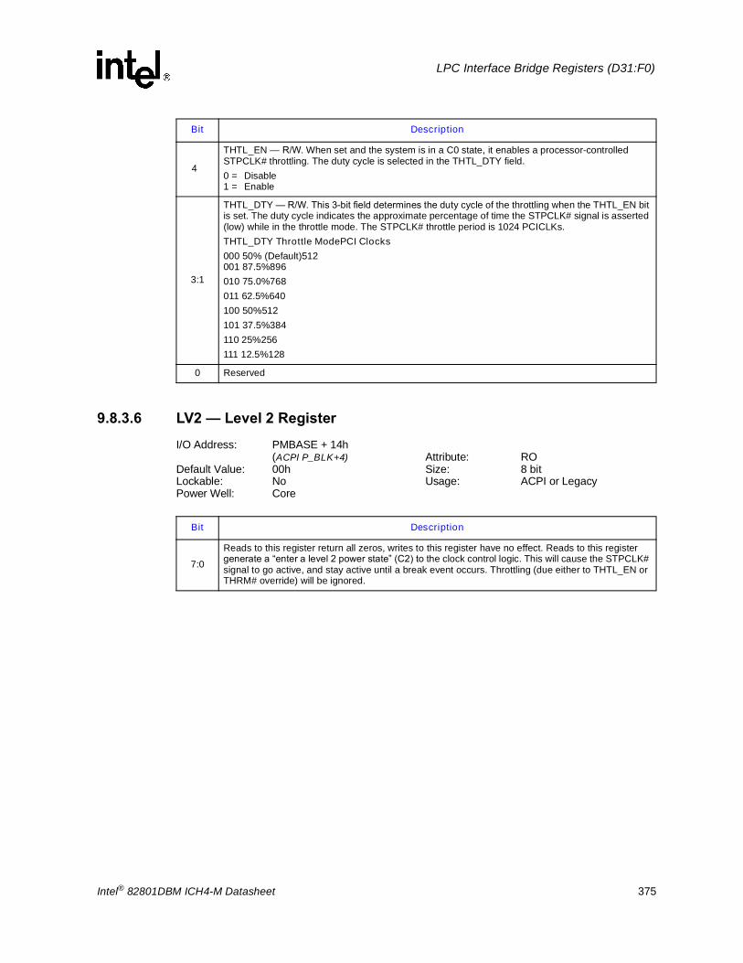
Intel® 82801DBM ICH4-M Datasheet 375
LPC Interface Bridge Registers (D31:F0)
9.8.3.6 LV2 � Level 2 RegisterI/O Address: PMBASE + 14h
(ACPI P_BLK+4) Attribute: RODefault Value: 00h Size: 8 bitLockable: No Usage: ACPI or LegacyPower Well: Core
4
THTL_EN � R/W. When set and the system is in a C0 state, it enables a processor-controlled STPCLK# throttling. The duty cycle is selected in the THTL_DTY field.0 = Disable1 = Enable
3:1
THTL_DTY � R/W. This 3-bit field determines the duty cycle of the throttling when the THTL_EN bit is set. The duty cycle indicates the approximate percentage of time the STPCLK# signal is asserted (low) while in the throttle mode. The STPCLK# throttle period is 1024 PCICLKs. THTL_DTY Throttle ModePCI Clocks000 50% (Default)512001 87.5%896010 75.0%768011 62.5%640100 50%512101 37.5%384110 25%256111 12.5%128
0 Reserved
Bit Description
Bit Description
7:0Reads to this register return all zeros, writes to this register have no effect. Reads to this register generate a �enter a level 2 power state� (C2) to the clock control logic. This will cause the STPCLK# signal to go active, and stay active until a break event occurs. Throttling (due either to THTL_EN or THRM# override) will be ignored.

376 Intel® 82801DBM ICH4-M Datasheet
LPC Interface Bridge Registers (D31:F0)
9.8.3.7 LV3�Level 3 RegisterI/O Address: PMBASE + 15h (ACPI P_BLK + 5)
Attribute: RODefault Value: 00h Size: 8 bitLockable: No Usage: ACPI or Legacy
Power Well: Core
NOTE: If the C4onC3_EN bit is set, the LV3 read will initiate a LV4 transition rather than a LV3 transition.
9.8.3.8 LV4�Level 4 RegisterI/O Address: PMBASE + 16h (ACPI P_BLK + 6)
Attribute: RODefault Value: 00h Size: 8 bitLockable: No Usage: ACPI or Legacy
Power Well: Core
9.8.3.9 PM2_CNT�Power Management 2 ControlI/O Address: PMBASE + 20h
(ACPI PM2_BLK) Attribute: R/WDefault Value: 00h Size: 8 bitLockable: No Usage: ACPIPower Well: Core
Bit Description
7:0Reads to this register return all zeros, writes to this register have no effect. Reads to this register generate a �enter a C3 power state� to the clock control logic. The C3 state persists until a break event occurs.
Bit Description
7:0Reads to this register return all zeros, writes to this register have no effect. Reads to this register generate a �enter a C4 power state� to the clock control logic. The C4 state persists until a break event occurs.
Bit Description
7:1 Reserved
0
Arbiter Disable (ARB_DIS) � R/W0 = Enable Hub Interface arbiter1 = Disable Hub Interface arbiter. ARB_DIS will only disable the arbiter at the Hub Interface to
prevent up-bound traffic. Consequently, the PCI arbiter will continue to issue GNT#s even when ARB_DIS is set. Note that after the arbiter is disabled, the processor must not initiate down-bound reads to PCI devices that may have up-bound posted data, as this will result in system deadlock.
NOTES:1. In general, software should not attempt any non-posted accesses during arbiter disable except to
the ICH4's power management registers. This implies that interrupt handlers for any unmasked hardware interrupts and SMI/NMI should check ARB_DIS status before reading from ICH devices.

Intel® 82801DBM ICH4-M Datasheet 377
LPC Interface Bridge Registers (D31:F0)
9.8.3.10 GPE0_STS�General Purpose Event 0 Status RegisterI/O Address: PMBASE + 28h
(ACPI GPE0_BLK) Attribute: R/WC, R/WDefault Value: 00000000h Size: 32 bitLockable: No Usage: ACPIPower Well: Resume
Note: This register is symmetrical to the General Purpose Event 0 Enable Register. If the corresponding _EN bit is set, then when the _STS bit gets set, the ICH4 generates a Wake Event. Once back in an S0 state (or if already in an S0 state when the event occurs), the ICH4 also generates an SCI if the SCI_EN bit is set, or an SMI# if the SCI_EN bit is not set. There is no SCI/SMI# or wake event on THRMOR_STS since there is no corresponding _EN bit. None of these bits are reset by CF9h write. All are reset by RSMRST#.
Bit Description
31:16
GPIn_STS � R/WC. These bits are set any time the corresponding GPIO is set up as an input and the corresponding GPIO signal is high (or low if the corresponding GP_INV bit is set). If the corresponding enable bit is set in the GPE0_EN register, then when the GPI[n]_STS bit is set:
� If the system is in an S1-M�S5 state, the event will also wake the system.� If the system is in an S0 state (or upon waking back to an S0 state), a SCI will be caused
depending on the GPI_ROUT bits for the corresponding GPI.15:14 Reserved
13
PME_B0_STS � R/WC. 0 = Software clears this bit by writing a 1 to the bit position. (default)1 = This bit will be set to 1 by the ICH4 when any internal device on bus 0 asserts the equivalent
of the PME# signal. Additionally, if the PME_B0_EN bit is set, and the system is in an S0 state, then the setting of the PME_B0_STS bit will generate an SCI (or SMI# if SCI_EN is not set). If the PME_B0_STS bit is set, and the system is in an S1-M�S4 state (or S5 state due to SLP_TYP and SLP_EN), then the setting of the PME_B0_STS bit will generate a wake event, and an SCI (or SMI# if SCI_EN is not set) will be generated. If the system is in an S5 state due to power button override, then the PME_B0_STS bit will not cause a wake event or SCI.
12
USB3_STS � R/W0 = Disable.1 = Set by hardware and can be reset by writing a one to this bit position or a resume-well reset.
This bit is set when USB UHCI Controller #3 needs to cause a wake. Additionally if the USB3_EN bit is set, the setting of the USB3_STS bit will generate a wake event.
11
PME_STS � R/WC. 0 = Software clears this bit by writing a 1 to the bit position.1 = Set by hardware when the PME# signal goes active. Additionally, if the PME_EN bit is set,
and the system is in an S0 state, then the setting of the PME_STS bit will generate an SCI or SMI# (if SCI_EN is not set). If the PME_EN bit is set, and the system is in an S1-M�S4 state (or S5 state due to setting SLP_TYP and SLP_EN), then the setting of the PME_STS bit will generate a wake event, and an SCI will be generated. If the system is in an S5 state due to power button override or a power failure, then PME_STS will not cause a wake event or SCI.
10BATLOW_STS � R/WC.0 = Software clears this bit by writing a 1 to the bit position.1 = Set by hardware when the BATLOW# signal is asserted.
9
Global Standby Timer Status (GST_STS) � R/WC. 0 = Software clears this bit by writing a 1 to the bit position.1 = Set by hardware to indicate that the wake event was due to GST timeout. This bit will only be
set when the system was in the S1-M state.
8RI_STS � R/WC.0 = Software clears this bit by writing a 1 to the bit position.1 = Set by hardware when the RI# input signal goes active.

378 Intel® 82801DBM ICH4-M Datasheet
LPC Interface Bridge Registers (D31:F0)
7
SMBus Wake Status (SMB_WAK_STS) � R/WC. The SMBus controller can independently cause an SMI# or SCI, so this bit does not need to do so (unlike the other bits in this register).0 = Software clears this bit by writing a 1 to the bit position.1 = Set by hardware to indicate that the wake event was caused by the ICH4�s SMBus logic.This
bit will be set by the WAKE/SMI# command type, even if the system is already awake. The SMI handler should then clear this bit.
NOTES:1. This bit is set by the SMBus slave command 01h (Wake/SMI#) even when the system is in the
S0 state. Therefore, to avoid an instant wake on subsequent transitions to sleep states, software must clear this bit after each reception of the Wake/SMI# command or just prior to entering the sleep state.
2. If SMB_WAK_STS is set due to SMBus slave receiving a message, it will be cleared by internal logic when a THRMTRIP# event happens or a Power Button Override event. However, THRMTRIP# or Power Button Override event will not clear SMB_WAK_STS if it is set due to SMBALERT# signal going active.
3. The SMBALERT_STS bit (D31:F3:I/O Offset 00h:Bit 5) should be cleared by software before this bit is cleared.
6TCOSCI_STS � R/WC. 0 = Software clears this bit by writing a 1 to the bit position.1 = Set by hardware when the TCO logic causes an SCI.
5
AC97_STS � R/WC. This bit will be set to 1 by when the codecs are attempting to wake the system and the PME events for the codecs are armed for wakeup. A PME is armed by programming the appropriate PMEE bit in the Power Management Control and Status register at bit 8 of offset 54h in each AC�97 function. 0 = Software clears this bit by writing a 1 to the bit position.1 = Set by hardware when the codecs are attempting to wake the system. The AC97_STS bit
gets set only from the following two cases:� The PMEE bit for the function is set, and o The AC-link bit clock has been shut and the routed
AC_SDIN line is high (for audio, if routing is disabled, no wake events are allowed. � For modem, if audio routing is disabled, then the wake event is an OR of all AC_SDIN lines. If
routing is enabled, then the wake event for modem is the remaining non-routed AC_SDIN line), or o GPI Status Change Interrupt bit (NABMBAR + 30h, bit 0) is 1.
This bit is not affected by a hard reset caused by a CF9h write.
4
USB2_STS � R/WC.0 = Software clears this bit by writing a 1 to the bit position.1 = Set by hardware when USB UHCI Controller 2 needs to cause a wake. Wake event will be
generated if the corresponding USB2_EN bit is set.
3
USB1_STS � R/WC.0 = Software clears this bit by writing a 1 to the bit position.1 = Set by hardware when USB UHCI Controller 1 needs to cause a wake. Wake event will be
generated if the corresponding USB1_EN bit is set.2 Reserved
1
Thermal Interrupt Override Status (THRMOR_STS) � R/WC.0 = Software clears this bit by writing a 1 to the bit position.1 = This bit is set by hardware anytime a thermal over-ride condition occurs and starts throttling
the processor�s clock at the THRM_DTY ratio. This will not cause an SMI#, SCI, or wake event.
0
Thermal Interrupt Status (THRM_STS) � R/WC. 0 = Software clears this bit by writing a 1 to the bit position.1 = Set by hardware anytime the THRM# signal is driven active as defined by the THRM_POL
bit. Additionally, if the THRM_EN bit is set, then the setting of the THRM_STS bit will also generate a power management event (SCI or SMI#).
Bit Description

Intel® 82801DBM ICH4-M Datasheet 379
LPC Interface Bridge Registers (D31:F0)
9.8.3.11 GPE0_EN�General Purpose Event 0 Enables RegisterI/O Address: PMBASE + 2Ch
(ACPI GPE0_BLK + 2) Attribute: R/WDefault Value: 00000000h Size: 32-bitLockable: No Usage: ACPIPower Well: Bits 0�7, 12, 16�31 Resume,
Bits 8�11, 13�15 RTC
Note: This register is symmetrical to the General Purpose Event 0 Status Register. All the bits in this register should be cleared to 0 based on a Power Button Override. The resume well bits are all cleared by RSMRST#. The RTC sell bits are cleared by RTCRST#.
Bit Description
31:16 GPIn_EN � R/W. These bits enable the corresponding GPI[n]_STS bits being set to cause a SCI, and/or wake event. These bits are cleared by RSMRST#.
15:14 Reserved
13PME_B0_EN � R/W. Enables the setting of the PME_B0_STS bit to generate a wake event and/or an SCI or SMI#. PME_B0_STS can be a wake event from the S1-M�S4 states, or from S5 (if entered via SLP_TYP and SLP_EN) or power failure, but not Power Button Override. This bit defaults to 0. It is only cleared by Software or RTCRST#. It is not cleared by CF9h writes.
12
USB3_EN � R/W.0 = Disable.1 = Enable the setting of the USB3_STS bit to generate a wake event. The USB3_STS bit is set
anytime USB UHCI Controller #3 signals a wake event. Break events are handled via the USB interrupt.
11
PME_EN � R/W.0 = Disable.1 = Enables the setting of the PME_STS to generate a wake event and/or an SCI. PME# can be
a wake event from the S1-M�S4 state or from S5 (if entered via SLP_EN, but not power button override).
10
BATLOW_EN � R/W. 0 = Disable.1 = Enables the BATLOW# signal to cause an SMI# or SCI (depending on the SCI_EN bit) when
it goes low. This bit does not prevent the BATLOW# signal from inhibiting the wake event.
9 Reserved
8
RI_EN � R/W. The value of this bit will be maintained through a G3 state and is not affected by a hard reset caused by a CF9h write.0 = Disable.1 = Enables the setting of the RI_STS to generate a wake event.
7 Reserved
6TCOSCI_EN � R/W.0 = Disable.1 = Enables the setting of the TCOSCI_STS to generate an SCI.
5AC97_EN � R/W.0 = Disable.1 = Enables the setting of the AC97_STS to generate a wake event.
4
USB2_EN � R/W.0 = Disable.1 = Enable the setting of the USB2_STS bit to generate a wake event. The USB2_STS bit is set
anytime USB UHCI Controller #2 signals a wake event. Break events are handled via the USB interrupt.

380 Intel® 82801DBM ICH4-M Datasheet
LPC Interface Bridge Registers (D31:F0)
9.8.3.12 SMI_EN�SMI Control and Enable RegisterI/O Address: PMBASE + 30h Attribute: R/W, WO, R/W-SpecialDefault Value: 0000h Size: 32 bitLockable: No Usage: ACPI or Legacy Power Well: Core
3
USB1_EN � R/W.0 = Disable.1 = Enable the setting of the USB1_STS bit to generate a wake event. The USB1_STS bit is set
anytime USB UHCI Controller #1 signals a wake event. Break events are handled via the USB interrupt.
2
THRM#_POL � R/W. This bit controls the polarity of the THRM# pin needed to set the THRM_STS bit. 0 = Low value on the THRM# signal will set the THRM_STS bit.1 = HIGH value on the THRM# signal will set the THRM_STS bit.
1 Reserved
0
THRM_EN � R/W.0 = Disable.1 = Active assertion of the THRM# signal (as defined by the THRM_POL bit) will set the
THRM_STS bit and generate a power management event (SCI or SMI).
Bit Description
Bit Description
31:19 Reserved
18INTEL_USB2_EN � R/W. 0 = Disable.1 = Enables Intel-Specific USB EHCI SMI logic to cause SMI#.
17LEGACY_USB2_EN � R/W. 0 = Disable.1 = Enables legacy USB EHCI logic to cause SMI#.
16:15 Reserved
14
PERIODIC_EN � R/W.0 = Disable.1 = Enables the ICH4 to generate an SMI# when the PERIODIC_STS bit is set in the SMI_STS
register.
13
TCO_EN � R/W.0 = Disables TCO logic generating an SMI#. Note that if the NMI2SMI_EN bit is set, SMIs that are
caused by re-routed NMIs will not be gated by the TCO_EN bit. Even if the TCO_EN bit is 0, NMIs will still be routed to cause SMIs.
1 = Enables the TCO logic to generate SMI#.
12 Reserved
11
Microcontroller SMI Enable (MCSMI_EN) � R/W.0 = Disable.1 = Enables ICH4 to trap accesses to the microcontroller range (62h or 66h) and generate an
SMI#. Note that �trapped� cycles will be claimed by the ICH4 on PCI, but not forwarded to LPC.
10:8 Reserved

Intel® 82801DBM ICH4-M Datasheet 381
LPC Interface Bridge Registers (D31:F0)
7
BIOS Release (BIOS_RLS) � WO.0 = This bit will always return 0 on reads. Writes of 0 to this bit have no effect.1 = Enables the generation of an SCI interrupt for ACPI software when a one is written to this bit
position by BIOS software.
6
Software SMI# Timer Enable (SWSMI_TMR_EN) � R/W.0 = Disable. Clearing the SWSMI_TMR_EN bit before the timer expires will reset the timer and the
SMI# will not be generated.1 = Starts Software SMI# Timer. When the SWSMI timer expires (the timeout period depends upon
the SWSMI_RATE_SEL bit setting), SWSMI_TMR_STS is set and an SMI# is generated. SWSMI_TMR_EN stays set until cleared by software.
5APMC_EN � R/W.0 = Disable. Writes to the APM_CNT register will not cause an SMI#.1 = Enables writes to the APM_CNT register to cause an SMI#.
4
SLP_SMI_EN � R/W.0 = Disables the generation of SMI# on SLP_EN. Note that this bit must be 0 before the software
attempts to transition the system into a sleep state by writing a 1 to the SLP_EN bit.1 = A write of 1 to the SLP_EN bit (bit 13 in PM1_CNT register) will generate an SMI#, and the
system will not transition to the sleep state based on that write to the SLP_EN bit.
3LEGACY_USB_EN � R/W.0 = Disable.1 = Enables legacy USB circuit to cause SMI#.
2BIOS_EN � R/W.0 = Disable.1 = Enables the generation of SMI# when ACPI software writes a 1 to the GBL_RLS bit.
1
End of SMI (EOS) � R/W-Special. This bit controls the arbitration of the SMI signal to the processor. This bit must be set for the ICH4 to assert SMI# low to the processor. 0 = Once the ICH4 asserts SMI# low, the EOS bit is automatically cleared.1 = When this bit is set, SMI# signal will be deasserted for 4 PCI clocks before its assertion. In the
SMI handler, the CPU should clear all pending SMIs (by servicing them and then clearing their respective status bits), set the EOS bit, and exit SMM. This will allow the SMI arbiter to re-assert SMI upon detection of an SMI event and the setting of a SMI status bit.
NOTE: ICH4 is able to generate 1st SMI after reset even though EOS bit is not set. Subsequent SMI require EOS bit is set.
0GBL_SMI_EN � R/W.0 = No SMI# will be generated by ICH4. This bit is reset by a PCI reset event.1 = Enables the generation of SMI# in the system upon any enabled SMI event.
Bit Description

382 Intel® 82801DBM ICH4-M Datasheet
LPC Interface Bridge Registers (D31:F0)
9.8.3.13 SMI_STS�SMI Status RegisterI/O Address: PMBASE + 34h Attribute: R/WC, RODefault Value: 0000h Size: 32-bitLockable: No Usage: ACPI or Legacy Power Well: Core
Note: If the corresponding _EN bit is set when the _STS bit is set, the ICH4 will cause an SMI# (except bits 8:10 and 12, which don�t need enable bits since they are logic ORs of other registers that have enable bits). The ICH4 uses the same GPE0_EN register (I/O address: PMBase+2Ch) to enable/disable both SMI and ACPI SCI general purpose input events. ACPI OS assumes that it owns the entire GPE0_EN register per ACPI spec. Problems arise when some of the general-purpose inputs are enabled as SMI by BIOS, and some of the general purpose inputs are enabled for SCI. In this case ACPI OS turns off the enabled bit for any GPIx input signals that are not indicated as SCI general-purpose events at boot, and exit from sleeping states. BIOS should define a dummy control method which prevents the ACPI OS from clearing the SMI GPE0_EN bits.
Bit Description
31:19 Reserved
18INTEL_USB2_STS � RO. This non-sticky read-only bit is a logical OR of each of the SMI status bits in the Intel-Specific USB EHCI SMI Status Register ANDed with the corresponding enable bits. This bit will not be active if the enable bits are not set. Writes to this bit have no effect.
17LEGACY_USB2_STS � RO. This non-sticky read-only bit is a logical OR of each of the SMI status bits in the USB EHCI Legacy Support Register ANDed with the corresponding enable bits. This bit will not be active if the enable bits are not set. Writes to this bit will have no effect.
16
SMBus SMI Status (SMBUS_SMI_STS) � R/WC.0 = This bit is cleared by writing a 1 to its bit position. This bit is set from the 64 KHz clock domain
used by the SMBus. Software must wait at least 15.63 us after the initial assertion of this bit before clearing it.
1 = Indicates that the SMI# was caused by:�The SMBus Slave receiving a message, or�The SMBALERT# signal goes active and the SMB_SMI_EN bit is set and the SMBALERT_DIS
bit is cleared, or�The SMBus Slave receiving a Host Notify message and the HOST_NOTIFY_INTREN and the
SMB_SMI_EN bits are set, or�The ICH4 detecting the SMLINK_SLAVE_SMI command while in the S0 state.
15SERIRQ_SMI_STS � RO.0 = SMI# was not caused by SERIRQ decoder. This is not a sticky bit.1 = SMI# was caused by the SERIRQ decoder.
14
PERIODIC_STS � R/WC.� This bit is cleared by writing a 1 to its bit position.
1 = This bit will be set at the rate determined by the PER_SMI_SEL bits. If the PERIODIC_EN bit is also set, the ICH4 will generate an SMI#.
13
TCO_STS � R/WC.0 = SMI# not caused by TCO logic.1 = SMI# was caused by the TCO logic. Note that this is not a wake event.Note: This bit is cleared by writing a 1 to this bit position.
12
Device Monitor Status (DEVMON_STS) � RO.0 = SMI# not caused by Device Monitor.1 = Set under any of the following conditions:
�Any of the DEV[7:4]_TRAP_STS bits are set and the corresponding DEV[7:4]_TRAP_EN bits are also set.
�Any of the DEVTRAP_STS bits are set and the corresponding DEVTRAP_EN bits are also set.

Intel® 82801DBM ICH4-M Datasheet 383
LPC Interface Bridge Registers (D31:F0)
11
Microcontroller SMI# Status (MCSMI_STS) � R/WC.0 = Indicates that there has been no access to the power management microcontroller range (62h or
66h). This bit is cleared by software writing a 1 to the bit position.1 = Set if there has been an access to the power management microcontroller range (62h or 66h). If
this bit is set and the MCSMI_EN bit is also set, the ICH4 will generate an SMI#.
10
GPE0_STS � RO. This bit is a logical OR of the bits in the ALT_GP_SMI_STS register that are also set up to cause an SMI# (as indicated by the GPI_ROUT registers) and have the corresponding bit set in the ALT_GP_SMI_EN register. Bits that are not routed to cause an SMI# will have no effect on this bit.0 = SMI# was not generated by a GPI assertion.1 = SMI# was generated by a GPI assertion.
9
GPE0_STS � RO. This bit is a logical OR of the bits in the GPE0_STS register that also have the corresponding bit set in the GPE0_EN register.0 = SMI# was not generated by a GPE0 event.1 = SMI# was generated by a GPE0 event.
8
PM1_STS_REG � RO. This is an ORs of the bits in the ACPI PM1 Status Register (offset PMBASE+00h) that can cause an SMI#.0 = SMI# was not generated by a PM1_STS event.1 = SMI# was generated by a PM1_STS event.
7 Reserved
6SWSMI_TMR_STS � R/WC. 0 = Software clears this bit by writing a 1 to the bit location.1 = Set by the hardware when the Software SMI# Timer expires.
5APM_STS � R/WC. 0 = Software clears this bit by writing a 1 to the bit location.1 = SMI# was generated by a write access to the APM control register with the APMC_EN bit set.
4SLP_SMI_STS � R/WC.0 = Software clears this bit by writing a 1 to the bit location.1 = Indicates an SMI# was caused by a write of 1 to SLP_EN bit when SLP_SMI_EN bit is also set.
3
LEGACY_USB_STS � RO. This bit is a logical OR of each of the SMI status bits in the USB Legacy Keyboard/Mouse Control Registers ANDed with the corresponding enable bits. This bit will not be active if the enable bits are not set.0 = SMI# was not generated by USB Legacy event.1 = SMI# was generated by USB Legacy event.
2
BIOS_STS � R/WC. 0 = Software clears this bit by writing a 1 to the bit location.1 = SMI# was generated due to ACPI software requesting attention (writing a 1 to the GBL_RLS bit
with the BIOS_EN bit set).
1:0 Reserved
Bit Description

384 Intel® 82801DBM ICH4-M Datasheet
LPC Interface Bridge Registers (D31:F0)
9.8.3.14 ALT_GP_SMI_EN�Alternate GPI SMI Enable RegisterI/O Address: PMBASE +38h Attribute: R/WDefault Value: 0000h Size: 16 bitLockable: No Usage: ACPI or LegacyPower Well: Resume
9.8.3.15 ALT_GP_SMI_STS�Alternate GPI SMI Status RegisterI/O Address: PMBASE +3Ah Attribute: R/WCDefault Value: 0000h Size: 16 bitLockable: No Usage: ACPI or LegacyPower Well: Resume
9.8.3.16 MON_SMI�Device Monitor SMI Status and Enable RegisterI/O Address: PMBASE +40h Attribute: R/W, R/WCDefault Value: 0000h Size: 16 bitLockable: No Usage: Legacy OnlyPower Well: Core
Bit Description
15:0
Alternate GPI SMI Enable � R/W. These bits are used to enable the corresponding GPIO to cause an SMI#. For these bits to have any effect, the following must be true.
� The corresponding bit in the ALT_GP_SMI_EN register is set.� The corresponding GPI must be routed in the GPI_ROUT register to cause an SMI.� The corresponding GPIO must be implemented.
Bit Description
15:0
Alternate GPI SMI Status � R/WC. These bits report the status of the corresponding GPIs. 1 = active, 0 = inactive. These bits are sticky. If the following conditions are true, an SMI# will be generated and the GPE0_STS bit set:
� The corresponding bit in the ALT_GPI_SMI_EN register is set� The corresponding GPI must be routed in the GPI_ROUT register to cause an SMI.� The corresponding GPIO must be implemented.
All bits are in the resume well. Default for these bits is dependent on the state of the GPI pins.
Bit Description
15:12
DEV[7:4]_TRAP_STS � R/WC. Bit 12 corresponds to Monitor 4, bit 13 corresponds to Monitor 5 etc.0 = SMI# was not caused by the associated device monitor.1 = SMI# was caused by an access to the corresponding device monitor�s I/O range.
11:8DEV[7:4]_TRAP_EN � R/W. Bit 8 corresponds to Monitor 4, bit 9 corresponds to Monitor 5 etc.0 = Disable.1 = Enables SMI# due to an access to the corresponding device monitor�s I/O range.
7:0 Reserved

Intel® 82801DBM ICH4-M Datasheet 385
LPC Interface Bridge Registers (D31:F0)
9.8.3.17 DEVACT_STS � Device Activity Status RegisterI/O Address: PMBASE +44h Attribute: R/WCDefault Value: 0000h Size: 16 bitLockable: No Usage: Legacy OnlyPower Well: Core
This register is used in conjunction with the Periodic SMI# timer to detect any system activity for legacy power management.
Bit Description
15:14 Reserved
13ADLIB_ACT_STS � R/WC. Ad-Lib.0 = Indicates that there has been no access to this device�s I/O range.1 = This device�s I/O range has been accessed. Clear this bit by writing a 1 to the bit location.
12KBC_ACT_STS � R/WC. KBC (60/64h). 0 = Indicates that there has been no access to this device�s I/O range.1 = This device�s I/O range has been accessed. Clear this bit by writing a 1 to the bit location.
11MIDI_ACT_STS � R/WC. MIDI.0 = Indicates that there has been no access to this device�s I/O range.1 = This device�s I/O range has been accessed. Clear this bit by writing a 1 to the bit location.
10AUDIO_ACT_STS � R/WC. Audio (Sound Blaster �OR�d� with MSS).0 = Indicates that there has been no access to this device�s I/O range.1 = This device�s I/O range has been accessed. Clear this bit by writing a 1 to the bit location.
9
PIRQDH_ACT_STS � R/WC. PIRQ[D or H].0 = The corresponding PCI interrupts have not been active.1 = At least one of the corresponding PCI interrupts has been active. Clear this bit by writing a 1 to
the bit location.
8
PIRQCG_ACT_STS � R/WC. PIRQ[C or G].0 = The corresponding PCI interrupts have not been active.1 = At least one of the corresponding PCI interrupts has been active. Clear this bit by writing a 1 to
the bit location.
7
PIRQBF_ACT_STS � R/WC. PIRQ[B or F].0 = The corresponding PCI interrupts have not been active.1 = At least one of the corresponding PCI interrupts has been active. Clear this bit by writing a 1 to
the bit location.
6
PIRQAE_ACT_STS � R/WC. PIRQ[A or E].0 = The corresponding PCI interrupts have not been active.1 = At least one of the corresponding PCI interrupts has been active. Clear this bit by writing a 1 to
the bit location.
5LEG_ACT_STS � R/WC. Parallel Port, Serial Port 1, Serial Port 2, Floppy Disk Controller.0 = Indicates that there has been no access to this device�s I/O range.1 = This device�s I/O range has been accessed. Clear this bit by writing a 1 to the bit location.
4 Reserved
3IDES1_ACT_STS � R/WC. IDE Secondary Drive 1.0 = Indicates that there has been no access to this device�s I/O range.1 = This device�s I/O range has been accessed. Clear this bit by writing a 1 to the bit location.
2IDES0_ACT_STS � R/WC. IDE Secondary Drive 0.0 = Indicates that there has been no access to this device�s I/O range.1 = This device�s I/O range has been accessed. Clear this bit by writing a 1 to the bit location.

386 Intel® 82801DBM ICH4-M Datasheet
LPC Interface Bridge Registers (D31:F0)
9.8.3.18 DEVTRAP_EN� Device Trap Enable RegisterI/O Address: PMBASE +48h Attribute: R/WDefault Value 0000h Size: 16 bitLockable: No Usage: Legacy OnlyPower Well: Core
This register enables the individual trap ranges to generate an SMI# when the corresponding status bit in the DEVACT_STS register is set. When a range is enabled, I/O cycles associated with that range will not be forwarded to LPC or IDE.
1IDEP1_ACT_STS � R/WC. IDE Primary Drive 1.0 = Indicates that there has been no access to this device�s I/O range.1 = This device�s I/O range has been accessed. Clear this bit by writing a 1 to the bit location.
0IDEP0_ACT_STS � R/WC. IDE Primary Drive 0.0 = Indicates that there has been no access to this device�s I/O range.1 = This device�s I/O range has been accessed. Clear this bit by writing a 1 to the bit location.
Bit Description
Bit Description
15:14 Reserved
13ADLIB_TRP_EN � R/W. Ad-Lib.0 = Disable.1 = Enable.
12KBC_TRP_EN � R/W. KBC (60/64h). 0 = Disable.1 = Enable.
11MIDI_TRP_EN � R/W. MIDI.0 = Disable.1 = Enable.
10AUDIO_TRP_EN � R/W. Audio (Sound Blaster �OR�d� with MSS).0 = Disable.1 = Enable.
9:6 Reserved
5LEG_IO_TRP_EN � R/W. Parallel Port, Serial Port 1, Serial Port 2, Floppy Disk Controller.0 = Disable.1 = Enable.
4 Reserved
3IDES1_TRP_EN � R/W. IDE Secondary Drive 1.0 = Disable.1 = Enable.
2IDES0_TRP_EN � R/W. IDE Secondary Drive 0.0 = Disable.1 = Enable.
1IDEP1_TRP_EN � R/W. IDE Primary Drive 1.0 = Disable.1 = Enable.

Intel® 82801DBM ICH4-M Datasheet 387
LPC Interface Bridge Registers (D31:F0)
9.8.3.19 BUS_ADDR_TRACK� Bus Address TrackerI/O Address: PMBASE +4Ch Attribute: ROLockable: No Size: 16 bitPower Well: Core Usage: Legacy Only
This register could be used by the SMI# handler to assist in determining what was the last cycle from the processor. BUS_ADDR_TRACK may not contain �expected� last I/O cycle data if Asynchronous SMIs and Synchronous SMIs are occurring simultaneously. This register only reports �expected� last I/O cycle data if Asynchronous SMIs are disabled.
9.8.3.20 BUS_CYC_TRACK� Bus Cycle TrackerI/O Address: PMBASE +4Eh Attribute: ROLockable: No Size: 8 bitPower Well: Core Usage: Legacy Only
This register could be used by the SMM handler to assist in determining what was the last cycle from the CPU. BUS_CYC_TRACK may not contain �expected� last I/O cycle data if Asynchronous SMIs and Synchronous SMIs are occurring simultaneously. This register only reports �expected� last I/O cycle data if Asynchronous SMIs are disabled.
0IDEP0_TRP_EN � R/W. IDE Primary Drive 0.0 = Disable.1 = Enable.
Bit Description
Bit Description
15:0Corresponds to the low 16 bits of the last I/O cycle, as would be defined by the PCI AD[15:0] signals on the PCI bus (even though it may not be a real PCI cycle). The value is latched based on SMI# active. This functionality is useful for figuring out which I/O was last being accessed.
Bit Description
7:4 Corresponds to the byte enables, as would be defined by the PCI C/BE# signals on the PCI bus (even though it may not be a real PCI cycle). The value is latched based on SMI# going active.
3:0 Corresponds to the cycle type, as would be defined by the PCI C/BE# signals on the PCI bus (even though it may not be a real PCI cycle). The value is latched based on SMI# going active.
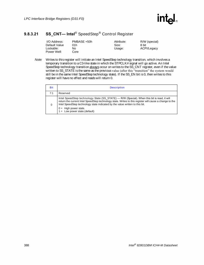
388 Intel® 82801DBM ICH4-M Datasheet
LPC Interface Bridge Registers (D31:F0)
9.8.3.21 SS_CNT� Intel® SpeedStep® Control Register
I/O Address: PMBASE +50h Attribute: R/W (special)Default Value 01h Size: 8 bitLockable: No Usage: ACPI/LegacyPower Well: Core
Note: Writes to this register will initiate an Intel SpeedStep technology transition, which involves a temporary transition to a C3-like state in which the STPCLK# signal will go active. An Intel SpeedStep technology transition always occur on writes to the SS_CNT register, even if the value written to SS_STATE is the same as the previous value (after this �transition� the system would still be in the same Intel SpeedStep technology state). If the SS_EN bit is 0, then writes to this register will have no effect and reads will return 0.
Bit Description
7:1 Reserved
0
Intel SpeedStep technology State (SS_STATE) � R/W (Special). When this bit is read, it will return the current Intel SpeedStep technology state. Writes to this register will cause a change to the Intel SpeedStep technology state indicated by the value written to this bit.0 = High power state.1 = Low power state.(default)

Intel® 82801DBM ICH4-M Datasheet 389
LPC Interface Bridge Registers (D31:F0)
9.9 System Management TCO Registers (D31:F0)The TCO logic is accessed via registers mapped to the PCI configuration space (Device 31:Function 0) and the system I/O space. For TCO PCI Configuration registers, see LPC Device 31:Function 0 PCI Configuration registers.
The TCO I/O registers reside in a 32-byte range pointed to by a TCOBASE value, which is, ACPIBASE + 60h in the PCI configuration space. Table 9-11 shows the mapping of the registers within that 32-byte range. Each register is described in the following sections.
9.9.1 TCO_RLD�TCO Timer Reload and Current Value RegisterI/O Address: TCOBASE +00h Attribute: R/WDefault Value: 00h Size: 8 bitLockable: No Power Well: Core
Table 9-11. TCO I/O Register Map
Offset Mnemonic Register Name Type
00h TCO_RLD TCO Timer Reload and Current Value R/W
01h TCO_TMR TCO Timer Initial Value R/W
02h TCO_DAT_IN TCO Data In R/W
03h TCO_DAT_OUT TCO Data Out R/W
04h�05h TCO1_STS TCO Status R/W, RO
06h�07h TCO2_STS TCO Status R/W
08h�09h TCO1_CNT TCO Control R/W, R/WC, R/W-Special
0Ah�0Bh TCO2_CNT TCO Control R/W
0Ch�0Dh TCO_MESSAGE1TCO_MESSAGE2 Used by BIOS to indicate POST/Boot progress R/W
0Eh TCO_WDSTATUS Watchdog Status Register R/W
0Fh � Reserved RO
10h SW_IRQ_GEN Software IRQ Generation Register R/W
11h�1Fh � Reserved RO
Bit Description
7:0 Reading this register will return the current count of the TCO timer. Writing any value to this register will reload the timer to prevent the timeout. Bits 7:6 will always be 0.

390 Intel® 82801DBM ICH4-M Datasheet
LPC Interface Bridge Registers (D31:F0)
9.9.2 TCO_TMR�TCO Timer Initial Value RegisterI/O Address: TCOBASE +01h Attribute: R/WDefault Value: 04h Size: 8 bitLockable: No Power Well: Core
9.9.3 TCO_DAT_IN�TCO Data In RegisterI/O Address: TCOBASE +02h Attribute: R/WDefault Value: 00h Size: 8 bitLockable: No Power Well: Core
9.9.4 TCO_DAT_OUT�TCO Data Out RegisterI/O Address: TCOBASE +03h Attribute: R/WDefault Value: 00h Size: 8 bitLockable: No Power Well: Core
Bit Description
7:6 Reserved
5:0Value that is loaded into the timer each time the TCO_RLD register is written. Values of 0h�1h will be ignored and should not be attempted. The timer is clocked at approximately 0.6 seconds, and this allows timeouts ranging from 2.4 seconds to 38 seconds.
Bit Description
7:0 Data Register for passing commands from the OS to the SMI handler. Writes to this register will cause an SMI and set the SW_TCO_SMI bit in the TCO1_STS register.
Bit Description
7:0Data Register for passing commands from the SMI handler to the OS. Writes to this register will set the TCO_INT_STS bit in the TCO_STS register. It will also cause an interrupt, as selected by the TCO_INT_SEL bits.

Intel® 82801DBM ICH4-M Datasheet 391
LPC Interface Bridge Registers (D31:F0)
9.9.5 TCO1_STS�TCO1 Status RegisterI/O Address: TCOBASE +04h Attribute: R/WC, RODefault Value: 0000h Size: 16 bitLockable: No Power Well: Core
(Except bit 7, in RTC)
Bit Description
15:13 Reserved
12
HUBSERR_STS � R/WC.0 = Software clears this bit by writing a 1 to the bit position.1 = ICH4 received an SERR# message via the hub interface. The software must read the memory
controller hub (or its equivalent) to determine the reason for the SERR#.
NOTE: If this bit is set AND the SERR_EN bit in CMD register (D30:F0, Offset 04h, bit 8) is also set, the ICH4 will set the SSE bit in SECSTS register (D30:F0, offset 1Eh, bit 14) AND will also generate a NMI (or SMI# if NMI routed to SMI#).
11
HUBNMI_STS � R/WC. 0 = Software clears this bit by writing a 1 to the bit position.1 = ICH4 received an NMI message via the hub interface. The software must read the memory
controller hub (or its equivalent) to determine the reason for the NMI.
10
HUBSMI_STS � R/WC. 0 = Software clears this bit by writing a 1 to the bit position.1 = ICH4 received an SMI message via the hub interface. The software must read the memory
controller hub (or its equivalent) to determine the reason for the SMI#.
9
HUBSCI_STS � R/WC.0 = Software clears this bit by writing a 1 to the bit position.1 = ICH4 received an SCI message via the hub interface. The software must read the memory
controller hub (or its equivalent) to determine the reason for the SCI.
8
BIOSWR_STS � R/WC.0 = Software clears this bit by writing a 1 to the bit position.1 = ICH4 sets this bit and generates and SMI# to indicate an illegal attempt to write to the BIOS.
This occurs when either: �The BIOSWP bit is changed from 0 to 1 and the BLD bit is also set, or �Any write is attempted to the BIOS and the BIOSWP bit is also set.
NOTE: On write cycles attempted to the 4-MB lower alias to the BIOS space, the BIOSWR_STS will not be set.
7
NEWCENTURY_STS � R/WC. This bit is in the RTC well.0 = Cleared by writing a 1 to the bit position or by RTCRST# going active.1 = This bit is set when the Year byte (RTC I/O space, index offset 09h) rolls over from 99 to 00.
Setting this bit will cause an SMI# (but not a wake event).Note that the NEWCENTURY_STS bit is not valid when the RTC battery is first installed (or when RTC power has not been maintained). Software can determine if RTC power has not been maintained by checking the RTC_PWR_STS bit, or by other means (e.g., a checksum on RTC RAM). If RTC power is determined to have not been maintained, BIOS should set the time to a legal value and then clear the NEWCENTURY_STS bit.The NEWCENTURY_STS bit may take up to 3 RTC clocks for the bit to be cleared after a 1 is written to the bit to clear it. After writing a 1 to this bit, software should not exit the SMI handler until verifying that the bit has actually been cleared. This will ensure that the SMI is not re-entered.
6:4 Reserved
3TIMEOUT � R/WC. 0 = Software clears this bit by writing a 1 to the bit position.1 = Set by ICH4 to indicate that the SMI was caused by the TCO timer reaching 0.

392 Intel® 82801DBM ICH4-M Datasheet
LPC Interface Bridge Registers (D31:F0)
9.9.6 TCO2_STS�TCO2 Status RegisterI/O Address: TCOBASE +06h Attribute: R/WCDefault Value: 0000h Size: 16 bitLockable: No Power Well: Resume
(Except Bit 0, in RTC)
2TCO_INT_STS � R/WC.0 = Software clears this bit by writing a 1 to the bit position.1 = SMI handler caused the interrupt by writing to the TCO_DAT_OUT register.
1SW_TCO_SMI � R/WC.0 = Software clears this bit by writing a 1 to the bit position.1 = Software caused an SMI# by writing to the TCO_DAT_IN register.
0
NMI2SMI_STS � RO.0 = Cleared by clearing the associated NMI status bit.1 = Set by the ICH4 when an SMI# occurs because an event occurred that would otherwise have
caused an NMI (because NMI2SMI_EN is set).
Bit Description
Bit Description
15:5 Reserved
4
SMLink Slave SMI Status (SMLINK_SLV_SMI_STS) � R/WC. This allow the software to go directly into pre-determined sleep state. This avoids race conditions.0 = The bit is reset by RSMRST#, but not due to the PCI Reset associated with exit from S3�S5
states. Software clears the bit by writing a 1 to this bit position. 1 = ICH4 sets this bit to 1 when it receives the SMI message on the SMLink's Slave Interface.
3 Reserved
2
BOOT_STS � R/WC. 0 = Cleared by ICH4 based on RSMRST# or by software writing a 1 to this bit. Note that software
should first clear the SECOND_TO_STS bit before writing a 1 to clear the BOOT_STS bit.1 = Set to 1 when the SECOND_TO_STS bit goes from 0 to 1 and the processor has not fetched the
first instruction. If rebooting due to a second TCO timer timeout, and if the BOOT_STS bit is set, the ICH4 will reboot using the �safe� multiplier (1111). This allows the system to recover from a CPU frequency multiplier that is too high, and allows the BIOS to check the BOOT_STS bit at boot. If the bit is set and the frequency multiplier is 1111, then the BIOS knows that the processor has been programmed to an illegal multiplier.
1
SECOND_TO_STS � R/WC.0 = This bit is cleared by writing a 1 to the bit position or by a RSMRST#.1 = The ICH4 sets this bit to a 1 to indicate that the TCO timer timed out a second time (probably due
to system lock). If this bit is set and the NO_REBOOT configuration bit is 0, then the ICH4 will reboot the system after the second timeout. The reboot is done by asserting PCIRST#.
NOTE: BIOS should always clear this bit before executing SMBus reads and writes.
0
Intruder Detect (INTRD_DET) � R/WC.0 = This bit is only cleared by writing a 1 to the bit position, or by RTCRST# assertion.1 = Set by ICH4 to indicate that an intrusion was detected. This bit is set even if the system is in G3
state.

Intel® 82801DBM ICH4-M Datasheet 393
LPC Interface Bridge Registers (D31:F0)
9.9.7 TCO1_CNT�TCO1 Control RegisterI/O Address: TCOBASE +08h Attribute: R/W, R/WC, R/W-SpecialDefault Value: 0000h Size: 16 bitLockable: No Power Well: Core
Bit Description
15:12 Reserved
11
TCO Timer Halt (TCO_TMR_HLT) � R/W.0 = The TCO Timer is enabled to count.1 = The TCO Timer will halt. It will not count, and thus cannot reach a value that will cause an SMI#
or set the SECOND_TO_STS bit. When set, this bit will prevent rebooting and prevent Alert On LAN event messages from being transmitted on the SMLINK (but not Alert On LAN* heartbeat messages).
10
SEND_NOW � R/W-Special. 0 = The ICH4 will clear this bit when it has completed sending the message. Software must not set
this bit to 1 again until the ICH4 has set it back to 0.1 = Writing a 1 to this bit will cause the ICH to send an Alert On LAN Event message over the
SMLINK interface, with the Software Event bit set.
NOTE: Setting the SEND_NOW bit causes the ICH4 integrated LAN Controller to reset, which can have unpredictable side-effects. Unless software protects against these side effects, software should not attempt to set this bit.
9
NMI2SMI_EN � R/W. 0 = Normal NMI functionality.1 = Forces all NMIs to instead cause SMIs. The functionality of this bit is dependent upon the
settings of the NMI_EN bit and the GBL_SMI_EN bit as detailed in the following table:NMI_ENGBL_SMI_ENDescription
00 No SMI# at all because GBL_SMI_EN = 001 SMI# will be caused due to NMI events10 No SMI# at all because GBL_SMI_EN = 011 No SMI# due to NMI because NMI_EN = 1
8
NMI_NOW � R/WC.0 = This bit is cleared by writing a 1 to the bit position. The NMI handler is expected to clear this bit.
Another NMI will not be generated until the bit is cleared.1 = Writing a 1 to this bit causes an NMI. This allows the BIOS or SMI handler to force an entry to
the NMI handler.
7:0 Reserved

394 Intel® 82801DBM ICH4-M Datasheet
LPC Interface Bridge Registers (D31:F0)
9.9.8 TCO2_CNT�TCO2 Control RegisterI/O Address: TCOBASE +0Ah Attribute: R/WDefault Value: 0008h Size: 16 bitLockable: No Power Well: Resume
9.9.9 TCO_MESSAGE1 and TCO_MESSAGE2 RegistersI/O Address: TCOBASE +0Ch (Message 1) Attribute: R/W
TCOBASE +0Dh (Message 2)Default Value: 00h Size: 8 bitLockable: No Power Well: Resume
Bit Description
15:4 Reserved
3
GPIO11_ALERT_DISABLE � R/W. At reset (via RSMRST# asserted) this bit is set and GPIO[11] alerts are disabled. 0 = Enable.1 = Disable GPIO11/SMBALERT# as an alert source for the heartbeats and the SMBus slave.
2:1
INTRD_SEL � R/W. Selects the action to take if the INTRUDER# signal goes active.00 = No interrupt or SMI#01 = Interrupt (as selected by TCO_INT_SEL).10 = SMI11 = Reserved
0 Reserved
Bit Description
7:0TCO_MESSAGE[n] � R/W.The value written into this register will be sent out via the SMLINK interface in the MESSAGE field of the Alert On LAN message. BIOS can write to this register to indicate its boot progress which can be monitored externally.
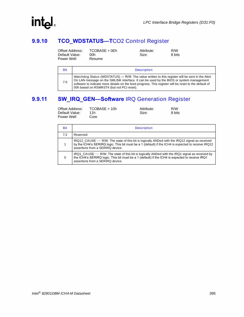
Intel® 82801DBM ICH4-M Datasheet 395
LPC Interface Bridge Registers (D31:F0)
9.9.10 TCO_WDSTATUS�TCO2 Control RegisterOffset Address: TCOBASE + 0Eh Attribute: R/WDefault Value: 00h Size: 8 bitsPower Well: Resume
9.9.11 SW_IRQ_GEN�Software IRQ Generation RegisterOffset Address: TCOBASE + 10h Attribute: R/WDefault Value: 11h Size: 8 bitsPower Well: Core
Bit Description
7:0Watchdog Status (WDSTATUS) � R/W. The value written to this register will be sent in the Alert On LAN message on the SMLINK interface. It can be used by the BIOS or system management software to indicate more details on the boot progress. This register will be reset to the default of 00h based on RSMRST# (but not PCI reset).
Bit Description
7:2 Reserved
1IRQ12_CAUSE � R/W. The state of this bit is logically ANDed with the IRQ12 signal as received by the ICH4�s SERIRQ logic. This bit must be a 1 (default) if the ICH4 is expected to receive IRQ12 assertions from a SERIRQ device.
0IRQ1_CAUSE � R/W. The state of this bit is logically ANDed with the IRQ1 signal as received by the ICH4�s SERIRQ logic. This bit must be a 1 (default) if the ICH4 is expected to receive IRQ1 assertions from a SERIRQ device.

396 Intel® 82801DBM ICH4-M Datasheet
LPC Interface Bridge Registers (D31:F0)
9.10 General Purpose I/O Registers (D31:F0)The control for the general purpose I/O signals is handled through a separate 64-byte I/O space. The base offset for this space is selected by the GPIO_BAR register. Table 9-12 shows the GPIO Register I/O address map.
Table 9-12. Registers to Control GPIO
Offset Mnemonic Register Name Default Access
General Registers
00�03h GPIO_USE_SEL GPIO Use Select 1A003180h R/W
04�07h GP_IO_SEL GPIO Input/Output Select 0000 FFFFh R/W
08�0Bh � Reserved 00h RO
0C�0Fh GP_LVL GPIO Level for Input or Output 1B3F 0000h R/W
10�13h � Reserved 00h RO
Output Control Registers
14�17h GPO_TTL GPIO TTL Select 06630000h RO
18�1Bh GPO_BLINK GPIO Blink Enable 00040000h R/W
1C�1Fh � Reserved 0 RO
Input Control Registers
20�2Bh � Reserved 00000000h RO
2C�2Fh GPI_INV GPIO Signal Invert 00000000h R/W
30�33h GPIO_USE_SEL2 GPIO Use Select 00000FFFh R/W
34�37h GP_IO_SEL2 GPIO Input/Output Select 2 00000000h R/W
38�3Bh GP_LVL2 GPIO Level for Input or Output 2 00000FFFh R/W

Intel® 82801DBM ICH4-M Datasheet 397
LPC Interface Bridge Registers (D31:F0)
9.10.1 GPIO_USE_SEL�GPIO Use Select RegisterOffset Address: GPIOBASE + 00h Attribute: R/WDefault Value: 1A003180h Size: 32-bitLockable: Yes Power Well: Resume
9.10.2 GP_IO_SEL�GPIO Input/Output Select RegisterOffset Address: GPIOBASE +04h Attribute: R/WDefault Value: 0000FFFFh Size: 32-bitLockable: No Power Well: Resume
Bit Description
21,11,5:0
GPIO_USE_SEL � R/W. Each bit in this register enables the corresponding GPIO (if it exists) to be used as a GPIO, rather than for the native function.0 = Signal used as native function.1 = Signal used as a GPIO.
NOTES:1. . Bits 31:29, 26, 24:18,15:14, 10:9, and 6 are not implemented because there is no
corresponding GPIO.2. Bits 28:27, 25, 13:12 and 8:7 are not implemented because the corresponding GPIOs are not
multiplexed.1. Bits 16:17 are not implemented because the GPIO selection is controlled by bits 0:1. The REQ/
GNT# pairs are enabled/disabled together. For example, if bit 0 is set to 1, then the REQ/GNT[A]# pair will function as GPIO[0] and GPIO[16].
Bit Description
31:29, 26 Reserved
28:2725
GPIO[n]_SEL � R/W.0 = Output. The corresponding GPIO signal is an output.1 = Input. The corresponding GPIO signal is an input.
24:18, Reserved
17:16 Always 0. The GPIOs are fixed as outputs.
15:0 Always 1. These GPIOs are fixed as inputs. NOTE: Bits 15:14, 10:9, 6 are not implemented and are reserved.

398 Intel® 82801DBM ICH4-M Datasheet
LPC Interface Bridge Registers (D31:F0)
9.10.3 GP_LVL�GPIO Level for Input or Output RegisterOffset Address: GPIOBASE +0Ch Attribute: R/W, RODefault Value: 1B3F 0000h Size: 32-bitLockable: No Power Well: See bit descriptions
9.10.4 GPO_BLINK�GPO Blink Enable RegisterOffset Address: GPIOBASE +18h Attribute: R/WDefault Value: 0004 0000h Size: 32-bitLockable: No Power Well: See bit description
Bit Description
31:29, 2624:18 Reserved
28:27, 25
GP_LVL[n] � R/W. If GPIO[n] is programmed to be an output (via the corresponding bit in the GP_IO_SEL register) then the bit can be updated by software to drive a high or low value on the output pin. If GPIO[n] is programmed as an input, then software can read the bit to determine the level on the corresponding input pin. These bits correspond to GPIO that are in the resume well, and will be reset to their default values by RSMRST# and also by a write to the CF9h register.0 = Low1 = High
17:16
GP_LVL[n] � R/W. These bits can be updated by software to drive a high or low value on the output pin. These bits correspond to GPIO that are in the core well, and will be reset to their default values by PCIRST#.0 = Low1 = High
15:0 Reserved. GPI[13:11], [8:7], and [5:0] the active status of a GPI is read from the corresponding bit in GPE0_STS register.
Bit Description
31:29, 26, 24:18, 17:0 Reserved
28:27, 25
GP_BLINK[n] � R/W. The setting of these bits will have no effect if the corresponding GPIO is programmed as an input. These bits correspond to GPIO that are in the Resume well, and will be reset to their default values by RSMRST# or a write to the CF9h register.0 = The corresponding GPIO will function normally.1 = If the corresponding GPIO is programmed as an output, the output signal will blink at a
rate of approximately once per second. The high and low times have approximately 0.5 seconds each. The GP_LVL bit is not altered when this bit is set.

Intel® 82801DBM ICH4-M Datasheet 399
LPC Interface Bridge Registers (D31:F0)
9.10.5 GPI_INV�GPIO Signal Invert RegisterOffset Address: GPIOBASE +2Ch Attribute: R/WDefault Value: 00000000h Size: 32-bitLockable: No Power Well: See bit description
9.10.6 GPIO_USE_SEL2�GPIO Use Select 2 RegisterOffset Address: GPIOBASE +30h Attribute: R/WDefault Value: 00000FFFh Size: 32-bitLockable: No Power Well: Core
Bit Description
31:14, 10:9, 6 Reserved
13:11, 8
GP_INV[n] � R/W. These bits are used to allow both active-low and active-high inputs to cause SMI# or SCI. Note that in the S0 or S1-M state, the input signal must be active for at least 2 PCI clocks to ensure detection by the ICH4. In the S3, S4 or S5 states the input signal must be active for at least 2 RTC clocks to ensure detection. The setting of these bits will have no effect if the corresponding GPIO is programmed as an output. These bits correspond to GPIO that are in the Resume well, and will be reset to their default values by RSMRST# or a write to the CF9h register.0 = The corresponding GPI_STS bit will be set when the ICH4 detects the state of the input pin
to be high.1 = The corresponding GPI_STS bit will be set when the ICH4 detects the state of the input pin
to be low.
7, 5:0
GP_INV[n] � R/W. These bits are used to allow both active-low and active-high inputs to cause SMI# or SCI. Note that in the S0 or S1-M state, the input signal must be active for at least 2 PCI clocks to ensure detection by the ICH4. The setting of these bits will have no effect if the corresponding GPIO is programmed as an output. These bits correspond to GPIO that are in the Core well, and will be reset to their default values by PCIRST#.0 = The corresponding GPI_STS bit will be set when the ICH4 detects the state of the input pin
to be high.1 = The corresponding GPI_STS bit will be set when the ICH4 detects the state of the input pin
to be low.
Bit Description
31:0
GPIO_USE_SEL2[43:32]� R/W. Each bit in this register enables the corresponding GPIO (if it exists) to be used as a GPIO, rather than for the native function.0 = Signal used as native function.1 = Signal used as a GPIO.
NOTES:1. The following bits are not implemented because there is no corresponding GPIO: 31:122. If GPIO[n] does not exist, then the bit in this register will always read as 0 and writes will have
no effect.After a full reset (RSMRST#) all multiplexed signals in the resume and core wells are configured as their native function rather than as a GPIO. After just a PCIRST#, the GPIO in the core well are configured as their native function.

400 Intel® 82801DBM ICH4-M Datasheet
LPC Interface Bridge Registers (D31:F0)
9.10.7 GP_IO_SEL2�GPIO Input/Output Select 2 RegisterOffset Address: GPIOBASE +34h Attribute: R/WDefault Value: 00000000h Size: 32-bitLockable: No Power Well: Core
9.10.8 GP_LVL2�GPIO Level for Input or Output 2 RegisterOffset Address: GPIOBASE +38h Attribute: R/WDefault Value: 00000FFFh Size: 32-bitLockable: No Power Well: See below
Bit Description
31:12 Always 0. No corresponding GPIO.
11:0GP_IO_SEL2[43:32] � R/W. When set to a 1, the corresponding GPIO signal (if enabled in the GPIO_USE_SEL2 register) is programmed as an input. When set to 0, the GPIO signal is programmed as an output.
Bit Description
31:12 Reserved. Read-only 0
11:0
GP_LVL2[43:32] � R/W. If GPIO[n] is programmed to be an output (via the corresponding bit in the GP_IO_SEL2 register), then the corresponding GP_LVL2[n] bit can be updated by software to drive a high or low value on the output pin. 1 = high, 0 = low. If GPIO[n] is programmed as an input, then the corresponding GP_LVL2 bit reflects the state of the input signal (1 = high, 0 = low). Writes will have no effect.Since these bits correspond to GPIO that are in the core well, these bits will be reset by PCIRST#.

Intel® 82801DBM ICH4-M Datasheet 401
IDE Controller Registers (D31:F1)
10 IDE Controller Registers (D31:F1)
10.1 PCI Configuration Registers (IDE�D31:F1)Note: Registers that are not shown should be treated as Reserved (See Section 6.2 for details).
All of the IDE registers are in the core well. None can be locked.
NOTES:1. The ICH4 IDE controller is not arbitrated as a PCI device, therefore it does not need a master latency timer.2. Refer to the ICH4 Specification Update for the value of the Revision ID Register.
Table 10-1. PCI Configuration Register Address Map (IDE�D31:F1)
Offset Mnemonic Register Name Default Type
00�01h VID Vendor ID 8086h RO
02�03h DID Device ID 24CAh RO
04�05h CMD Command Register 00h R/W, RO
06�07h STS Device Status 0280h R/WC, RO
08h RID Revision ID See Note 2 RO
09h PI Programming Interface 8Ah RO
0Ah SCC Sub Class Code 01h RO
0Bh BCC Base Class Code 01h RO
0Dh MLT Master Latency Timer (Note 1) 00 RO
0Eh HTYPE Header Type 00h RO
10�13h PCMD_BAR Primary Command Block Base Address 00000001h R/W
14�17h PCNL_BAR Primary Control Block Base Address 00000001h R/W
18�1Bh SCMD_BAR Secondary Command Block Base Address 00000001h R/W
1C�1Fh SCNL_BAR Secondary Control Block Base Address 00000001h R/W
20�23h BAR Base Address Register 00000001h R/W
24�27h EXBAR Expansion BAR 00h R/W
2C�2Dh SVID Subsystem Vendor ID 00 R/WO
2E�2Fh SID Subsystem ID 00 R/WO
3C INTR_LN Interrupt Line 00 R/W
3D INTR_PN Interrupt Pin 01 R/W
40�41h IDE_TIMP Primary IDE Timing 0000h R/W
42�43h ID_TIMS Secondary IDE Timing 0000h R/W
44h SIDETIM Slave IDE Timing 00h R/W
48h SDMAC Synchronous DMA Control Register 00h R/W
4A�4Bh SDMATIM Synchronous DMA Timing Register 0000h R/W
54h IDE_CONFIG IDE I/O Configuration Register 00h R/W

402 Intel® 82801DBM ICH4-M Datasheet
IDE Controller Registers (D31:F1)
10.1.1 VID�Vendor ID Register (LPC I/F�D31:F1)Offset Address: 00�01h Attribute: RODefault Value: 8086h Size: 16 bitLockable: No Power Well: Core
10.1.2 DID�Device ID Register (LPC I/F�D31:F1)Offset Address: 02�03h Attribute: RODefault Value: 24CAh Size: 16 bitLockable: No Power Well: Core
10.1.3 CMD � Command Register (IDE�D31:F1)Address Offset: 04h�05h Attribute: R/W, RODefault Value: 00h Size: 16 bits
Bit Description
15:0 Vendor Identification Value � RO. This is a 16-bit value assigned to Intel. Intel VID = 8086h
Bit Description
15:0 Device Identification Value � RO. This is a 16-bit value assigned to the ICH4 IDE Controller.
Bit Description
15:10 Reserved
9 Fast Back to Back Enable (FBE) � RO. Reserved as 0.
8 SERR# Enable (SERR_EN) � RO. Reserved as 0.
7 Wait Cycle Control (WCC) � RO. Reserved as 0.
6 Parity Error Response (PER) � RO. Reserved as 0.
5 VGA Palette Snoop (VPS) � RO. Reserved as 0.
4 Postable Memory Write Enable (PMWE) � RO. Reserved as 0.
3 Special Cycle Enable (SCE) � RO. Reserved as 0.
2
Bus Master Enable (BME) � R/W. Controls the ICH4�s ability to act as a PCI master for IDE Bus Master transfers.0 = Disable1 = Enable
1
Memory Space Enable (MSE) � R/W.0 = Disables access.1 = Enables access to the IDE Expansion memory range. The EXBAR register (Offset 24h) must
be programmed before this bit is set.
NOTE: BIOS should set this bit to a 1.

Intel® 82801DBM ICH4-M Datasheet 403
IDE Controller Registers (D31:F1)
10.1.4 STS � Device Status Register (IDE�D31:F1)Address Offset: 06�07h Attribute: R/WC, RODefault Value: 0280h Size: 16 bits
10.1.5 REVID�Revision ID Register (IDE�D31:F1)Offset Address: 08h Attribute: RODefault Value: See Bit Description Size: 8 bits
0
I/O Space Enable (IOSE) � R/W. This bit controls access to the I/O space registers. 0 = Disables access to the Legacy or Native IDE ports (both Primary and Secondary) as well as
the Bus Master IO registers. 1 = Enable. Note that the Base Address register for the Bus Master registers should be
programmed before this bit is set.
NOTES:1. Separate bits are provided (IDE Decode Enable, in the IDE Timing register) to independently
disable the Primary or Secondary I/O spaces.2. When this bit is 0 and the IDE controller is in Native Mode, the Interrupt Pin Register (see
Section 10.1.19) will be masked (the interrupt will not be asserted). If an interrupt occurs while the masking is in place and the interrupt is still active when the masking ends, the interrupt will be allowed to be asserted.
Bit Description
Bit Description
15 Detected Parity Error (DPE) � RO. Reserved as 0.
14 Signaled System Error (SSE) � RO. Reserved as 0.
13Received Master Abort (RMA) � R/WC.0 = Cleared by writing a 1 to it.1 = Bus Master IDE interface function, as a master, generated a master-abort.
12 Reserved as 0 � RO.
11
Signaled Target Abort (STA) � R/WC.0 = Cleared by writing a 1 to it.1 = ICH4 IDE interface function is targeted with a transaction that the ICH4 terminates with a target
abort.
10:9DEVSEL# Timing Status (DEV_STS) � RO. 01 =Hardwired; however, the ICH4 does not have a real DEVSEL# signal associated with the IDE
unit, so these bits have no effect.
8 Data Parity Error Detected (DPED)� RO. Reserved as 0.
7 Fast Back to Back Capable (FB2BC)� RO. Reserved as 1.
6 User Definable Features (UDF)� RO. Reserved as 0.
5 66 MHz Capable (66MHZ_CAP)� RO. Reserved as 0.
4:0 Reserved
Bit Description
7:0 Revision Identification Value � RO. Refer to the ICH4 Specification Update for the value of the Revision ID Register.

404 Intel® 82801DBM ICH4-M Datasheet
IDE Controller Registers (D31:F1)
10.1.6 PI � Programming Interface Register (IDE�D31:F1)Address Offset: 09h Attribute: R/WDefault Value: 8Ah Size: 8 bits
10.1.7 SCC � Sub Class Code Register (IDE�D31:F1)Address Offset: 0Ah Attribute: RODefault Value: 01h Size: 8 bits
10.1.8 BCC � Base Class Code Register (IDE�D31:F1)Address Offset: 0Bh Attribute: RODefault Value: 01h Size: 8 bits
Bit Description
7 This read-only bit is a 1 to indicate that the ICH4 supports bus master operation
6:4 Reserved. Will always return 0.
3 SOP_MODE_CAP � RO. This read-only bit is a 1 to indicate that the secondary controller supports both legacy and native modes.
2
SOP_MODE_SEL � R/W. This read/write bit determines the mode that the secondary IDE channel is operating in.0 = Legacy-PCI mode (default)1 = Native-PCI mode
1 POP_MODE_CAP � RO. This read-only bit is a 1 to indicate that the primary controller supports both legacy and native modes.
0
POP_MODE_SEL � R/W. This read/write bit determines the mode that the primary IDE channel is operating in. 0 = Legacy-PCI mode (default)1 = Native-PCI mode
Bit Description
7:0Sub Class Code � RO.01h = IDE device, in the context of a mass storage device.
Bit Description
7:0 Base Class Code � RO.01 = Mass storage device

Intel® 82801DBM ICH4-M Datasheet 405
IDE Controller Registers (D31:F1)
10.1.9 MLT � Master Latency Timer Register (IDE�D31:F1)Address Offset: 0Dh Attribute: RODefault Value: 00h Size: 8 bits
10.1.10 PCMD_BAR�Primary Command Block Base Address Register (IDE�D31:F1)Address Offset: 10h�13h Attribute: R/WDefault Value: 00000001h Size: 32 bits
.
NOTE: This 8-byte I/O space is used in native mode for the Primary Controller�s Command Block.
10.1.11 PCNL_BAR�Primary Control Block Base Address Register (IDE�D31:F1)Address Offset: 14h�17h Attribute: R/WDefault Value: 00000001h Size: 32 bits
.
NOTE: This 4-byte I/O space is used in native mode for the Primary Controller�s Command Block.
Bit Description
7:0 Master Latency Timer Count (MLTC) � RO. Hardwired to 00h. The IDE controller is implemented internally, and is not arbitrated as a PCI device, so it does not need a Master Latency Timer.
Bit Description
31:16 Reserved
15:3 Base Address � R/W. Base address of the I/O space (8 consecutive I/O locations).
2:1 Reserved
0 Resource Type Indicator (RTE) � RO. his bit is set to one, indicating a request for I/O space.
Bit Description
31:16 Reserved
15:2 Base Address � R/W. Base address of the I/O space (4 consecutive I/O locations).
1 Reserved
0 Resource Type Indicator (RTE) � RO. This bit is set to one, indicating a request for I/O space.

406 Intel® 82801DBM ICH4-M Datasheet
IDE Controller Registers (D31:F1)
10.1.12 SCMD_BAR�Secondary Command Block Base Address Register (IDE D31:F1)Address Offset: 18h�1Bh Attribute: R/WDefault Value: 00000001h Size: 32 bits
NOTE: This 4-byte I/O space is used in native mode for the Secondary Controller�s Command Block.
10.1.13 SCNL_BAR�Secondary Control Block Base Address Register (IDE D31:F1)Address Offset: 1Ch�1Fh Attribute: R/WDefault Value: 00000001h Size: 32 bits
NOTE: This 4-byte I/O space is used in native mode for the Secondary Controller�s Command Block.
10.1.14 BM_BASE � Bus Master Base Address Register (IDE�D31:F1)Address Offset: 20h�23h Attribute: R/WDefault Value: 00000001h Size: 32 bits
The Bus Master IDE interface function uses Base Address register 5 to request a 16-byte I/O space to provide a software interface to the Bus Master functions. Only 12 bytes are actually used (6 bytes for primary, 6 bytes for secondary). Only bits [15:4] are used to decode the address.
Bit Description
31:16 Reserved
15:3 Base Address � R/W. Base address of the I/O space (8 consecutive I/O locations).
2:1 Reserved
0 Resource Type Indicator (RTE) � RO. This bit is set to one, indicating a request for I/O space.
Bit Description
31:16 Reserved
15:2 Base Address � R/W. Base address of the I/O space (4 consecutive I/O locations).
1 Reserved
0 Resource Type Indicator (RTE) � RO. This bit is set to one, indicating a request for I/O space.
Bit Description
31:16 Reserved
15:4 Base Address � R/W. Base address of the I/O space (16 consecutive I/O locations).
3:1 Reserved
0 Resource Type Indicator (RTE) � RO. Hardwired to 1, indicating a request for I/O space.

Intel® 82801DBM ICH4-M Datasheet 407
IDE Controller Registers (D31:F1)
10.1.15 EXBAR � Expansion Base Address Register (IDE�D31:F1)Address Offset: 24h�27h Attribute: R/WDefault Value: 00h Size: 32 bits
Note: This is a memory mapped BAR that requires 1 KB of DWord-aligned memory that is Intel reserved for future functionality. BIOS needs to program the base address for a 1-kB memory space.
10.1.16 IDE_SVID � Subsystem Vendor ID Register (IDE�D31:F1)Address Offset: 2Ch�2Dh Attribute: R/WODefault Value: 00h Size: 16 bitsLockable: No Power Well: Core
10.1.17 IDE_SID � Subsystem ID Register (IDE�D31:F1)Address Offset: 2Eh�2Fh Attribute: R/WODefault Value: 00h Size: 16 bitsLockable: No Power Well: Core
Bit Description
31:0 Intel Reserved for Future Functionality.
Bit Description
15:0
Subsystem Vendor ID (SVID) � R/Write-Once. The SVID register, in combination with the Subsystem ID (SID) register, enables the operating system (OS) to distinguish subsystems from each other. Software (BIOS) sets the value in this register. After that, the value can be read, but subsequent writes to this register have no effect. The value written to this register will also be readable via the corresponding SVID registers for the USB UHCI #1, USB UHCI #2, USB UHCI #3, and SMBus functions.
Bit Description
15:0
Subsystem ID (SID) � R/Write-Once. The SID register, in combination with the SVID register, enables the operating system (OS) to distinguish subsystems from each other. Software (BIOS) sets the value in this register. After that, the value can be read, but subsequent writes to this register have no effect. The value written to this register will also be readable via the corresponding SID registers for the USB UHCI #1, USB UHCI #2, USB UHCI #3, and SMBus functions.

408 Intel® 82801DBM ICH4-M Datasheet
IDE Controller Registers (D31:F1)
10.1.18 INTR_LN�Interrupt Line Register (IDE�D31:F1)Address Offset: 3Ch Attribute: R/WDefault Value: 00h Size: 8 bits
10.1.19 INTR_PN�Interrupt Pin Register (IDE�D31:F1)Address Offset: 3Dh Attribute: RODefault Value: 01h Size: 8 bits
10.1.20 IDE_TIM � IDE Timing Register (IDE�D31:F1)Address Offset: Primary: 40�41h Attribute: R/W
Secondary: 42�43hDefault Value: 0000h Size: 16 bits
This register controls the timings driven on the IDE cable for PIO and 8237 style DMA transfers. It also controls operation of the buffer for PIO transfers.
Bit Description
7:0 Interrupt Line (INT_LN) � R/W. It is to communicate to software the interrupt line that the interrupt pin is connected to.
Bit Description
7:3 Reserved
2:0Interrupt Pin (INT_PN) � RO. The value of 01h indicates to �software� that the ICH4 will drive INTA#. Note that this is only used in native mode. Also note that the routing to the internal interrupt controller does not necessarily relate to the value in this register. The IDE interrupt is in fact routed to PIRQ[C]# (IRQ18 in APIC mode).
Bit Description
15
IDE Decode Enable (IDE) � R/W. Individually enable/disable the Primary or Secondary decode. The IDE I/O Space Enable bit in the Command register must be set for this bit to have any effect. Additionally, separate configuration bits are provided (in the IDE I/O Configuration register) to individually disable the primary or secondary IDE interface signals, even if the IDE Decode Enable bit is set.0 = Disable.1 = Enables the ICH4 to decode the associated Command Blocks (1F0�1F7h for primary,
170�177h for secondary) and Control Block (3F6h for primary and 376h for secondary).This bit effects the IDE decode ranges for both legacy and native-Mode decoding. It also effects the corresponding primary or secondary memory decode range for IDE Expansion.
14Drive 1 Timing Register Enable (SITRE) � R/W.0 = Use bits 13:12, 9:8 for both drive 0 and drive 1.1 = Use bits 13:12, 9:8 for drive 0, and use the Slave IDE Timing register for drive 1.
13:12
IORDY Sample Point (ISP) � R/W. The setting of these bits determine the number of PCI clocks between IDE IOR#/IOW# assertion and the first IORDY sample point.00 = 5 clocks01 = 4 clocks10 = 3 clocks11 = Reserved

Intel® 82801DBM ICH4-M Datasheet 409
IDE Controller Registers (D31:F1)
11:10 Reserved
9:8
Recovery Time (RCT) � R/W. The setting of these bits determines the minimum number of PCI clocks between the last IORDY sample point and the IOR#/IOW# strobe of the next cycle.00 = 4 clocks01 = 3 clocks10 = 2 clocks11 = 1 clock
7
Drive 1 DMA Timing Enable (DTE1) � R/W.0 = Disable.1 = Enable the fast timing mode for DMA transfers only for this drive. PIO transfers to the IDE data
port will run in compatible timing.
6Drive 1 Prefetch/Posting Enable (PPE1) � R/W.0 = Disable.1 = Enable Prefetch and posting to the IDE data port for this drive.
5Drive 1 IORDY Sample Point Enable (IE1) � R/W.0 = Disable IORDY sampling for this drive.1 = Enable IORDY sampling for this drive.
4
Drive 1 Fast Timing Bank (TIME1) � R/W.0 = Accesses to the data port will use compatible timings for this drive.1 = When this bit =1 and bit 14 = 0, accesses to the data port will use bits 13:12 for the IORDY
sample point, and bits 9:8 for the recovery time. When this bit = 1 and bit 14 = 1, accesses to the data port will use the IORDY sample point and recover time specified in the slave IDE timing register.
3
Drive 0 DMA Timing Enable (DTE0) � R/W.0 = Disable1 = Enable fast timing mode for DMA transfers only for this drive. PIO transfers to the IDE data
port will run in compatible timing.
2Drive 0 Prefetch/Posting Enable (PPE0) � R/W.0 = Disable prefetch and posting to the IDE data port for this drive.1 = Enable prefetch and posting to the IDE data port for this drive.
1Drive 0 IORDY Sample Point Enable (IE0) � R/W.0 = Disable IORDY sampling is disabled for this drive.1 = Enable IORDY sampling for this drive.
0
Drive 0 Fast Timing Bank (TIME0) � R/W.0 = Accesses to the data port will use compatible timings for this drive.1 = Accesses to the data port will use bits 13:12 for the IORDY sample point, and bits 9:8 for the
recovery time.
Bit Description
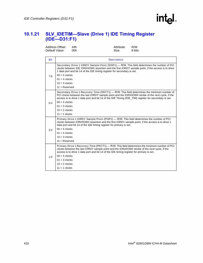
410 Intel® 82801DBM ICH4-M Datasheet
IDE Controller Registers (D31:F1)
10.1.21 SLV_IDETIM�Slave (Drive 1) IDE Timing Register (IDE�D31:F1)Address Offset: 44h Attribute: R/WDefault Value: 00h Size: 8 bits
Bit Description
7:6
Secondary Drive 1 IORDY Sample Point (SISP1) � R/W. This field determines the number of PCI clocks between IDE IOR#/IOW# assertion and the first IORDY sample point, if the access is to drive 1 data port and bit 14 of the IDE timing register for secondary is set.00 = 5 clocks01 = 4 clocks10 = 3 clocks11 = Reserved
5:4
Secondary Drive 1 Recovery Time (SRCT1) � R/W. This field determines the minimum number of PCI clocks between the last IORDY sample point and the IOR#/IOW# strobe of the next cycle, if the access is to drive 1 data port and bit 14 of the IDE Timing (IDE_TIM) register for secondary is set.00 = 4 clocks01 = 3 clocks10 = 2 clocks11 = 1 clocks
3:2
Primary Drive 1 IORDY Sample Point (PISP1) � R/W. This field determines the number of PCI clocks between IOR#/IOW# assertion and the first IORDY sample point, if the access is to drive 1 data port and bit 14 of the IDE timing register for primary is set.00 = 5 clocks01 = 4 clocks10 = 3 clocks11 = Reserved
1:0
Primary Drive 1 Recovery Time (PRCT1) � R/W. This field determines the minimum number of PCI clocks between the last IORDY sample point and the IOR#/IOW# strobe of the next cycle, if the access is to drive 1 data port and bit 14 of the IDE timing register for primary is set.00 = 4 clocks01 = 3 clocks10 = 2 clocks11 = 1 clocks

Intel® 82801DBM ICH4-M Datasheet 411
IDE Controller Registers (D31:F1)
10.1.22 SDMA_CNT�Synchronous DMA Control Register (IDE�D31:F1)Address Offset: 48h Attribute: R/W Default Value: 00h Size: 8 bits
Bit Description
7:4 Reserved
3Secondary Drive 1 Synchronous DMA Mode Enable (SSDE1) � R/W.0 = Disable (default)1 = Enable Synchronous DMA mode for secondary channel drive 1.
2Secondary Drive 0 Synchronous DMA Mode Enable (SSDE0) � R/W.0 = Disable (default)1 = Enable Synchronous DMA mode for secondary drive 0.
1Primary Drive 1 Synchronous DMA Mode Enable (PSDE1) � R/W.0 = Disable (default)1 = Enable Synchronous DMA mode for primary channel drive 1.
0Primary Drive 0 Synchronous DMA Mode Enable (PSDE0) � R/W.0 = Disable (default)1 = Enable Synchronous DMA mode for primary channel drive 0.

412 Intel® 82801DBM ICH4-M Datasheet
IDE Controller Registers (D31:F1)
10.1.23 SDMA_TIM�Synchronous DMA Timing Register (IDE�D31:F1)Address Offset: 4A�4Bh Attribute: R/WDefault Value: 0000h Size: 16 bits
Note: For FAST_SCB1=1 (133 MHz clk) in bits [13:12, 9:8, 5:4, 1:0], refer to Section 5.15.6 for details.
Bit Description
15:14 Reserved
13:12
Secondary Drive 1 Cycle Time (SCT1) � R/W. For Ultra ATA mode. The setting of these bits determines the minimum write strobe cycle time (CT). The DMARDY#-to-STOP (RP) time is also determined by the setting of these bits.SCB1 = 0 (33 MHz clk)SCB1 = 1 (66 MHz clk)FAST_SCB1 = 1 (133 MHz clk) 00 = CT 4 clocks, RP 6 clocks00 = Reserved00 = Reserved01 = CT 3 clocks, RP 5 clocks01 = CT 3 clocks, RP 8 clocks01 = CT 3 clks, RP 16 clks10 = CT 2 clocks, RP 4 clocks10 = CT 2 clocks, RP 8 clocks10 = Reserved11 = Reserved11 = Reserved11 = Reserved
11:10 Reserved
9:8
Secondary Drive 0 Cycle Time (SCT0) � R/W. For Ultra ATA mode. The setting of these bits determines the minimum write strobe cycle time (CT). The DMARDY#-to-STOP (RP) time is also determined by the setting of these bits.SCB1 = 0 (33 MHz clk)SCB1 = 1 (66 MHz clk)FAST_SCB1 = 1 (133 MHz clk)00 = CT 4 clocks, RP 6 clocks00 = Reserved00 = Reserved01 = CT 3 clocks, RP 5 clocks01 = CT 3 clocks, RP 8 clocks01 = CT 3 clks, RP 16 clks10 = CT 2 clocks, RP 4 clocks10 = CT 2 clocks, RP 8 clocks10 = Reserved11 = Reserved11 = Reserved11 = Reserved
7:6 Reserved
5:4
Primary Drive 1 Cycle Time (PCT1) � R/W. For Ultra ATA mode, the setting of these bits determines the minimum write strobe cycle time (CT). The DMARDY#-to-STOP (RP) time is also determined by the setting of these bits.PCB1 = 0 (33 MHz clk)PCB1 = 1 (66 MHz clk)FAST_PCB1 = 1 (133 MHz clk)00 = CT 4 clocks, RP 6 clocks00 = Reserved00 = Reserved01 = CT 3 clocks, RP 5 clocks01 = CT 3 clocks, RP 8 clocks01 = CT 3 clks, RP 16 clks10 = CT 2 clocks, RP 4 clocks10 = CT 2 clocks, RP 8 clocks10 = Reserved11 = Reserved11 = Reserved11 = Reserved
3:2 Reserved
1:0
Primary Drive 0 Cycle Time (PCT0) � R/W. For Ultra ATA mode, the setting of these bits determines the minimum write strobe cycle time (CT). The DMARDY#-to-STOP (RP) time is also determined by the setting of these bits.PCB1 = 0 (33 MHz clk)PCB1 = 1 (66 MHz clk)FAST_PCB1 = 1 (133 MHz clk)00 = CT 4 clocks, RP 6 clocks00 = Reserved00 = Reserved01 = CT 3 clocks, RP 5 clocks01 = CT 3 clocks, RP 8 clocks01 = CT 3 clks, RP 16 clks10 = CT 2 clocks, RP 4 clocks10 = CT 2 clocks, RP 8 clocks10 = Reserved11 = Reserved11 = Reserved11 = Reserved

Intel® 82801DBM ICH4-M Datasheet 413
IDE Controller Registers (D31:F1)
10.1.24 IDE_CONFIG�IDE I/O Configuration Register (IDE�D31:F1)Address Offset: 54h Attribute: R/WDefault Value: 00h Size: 32 bits
Bit Description
31:20 Reserved
19:18
SEC_SIG_MODE � R/W. These bits are used to control the mode of the Secondary IDE signal pins. If the SRS bit (bit 7, offset D5h of D31:F0) is 1, the reset states of bits 19:18 will be 01 (tri-state) instead of 00 (normal). 00 = Normal (Enabled)01 = Tri-state (Disabled)10 = Drive low (Disabled)11 = Reserved
17:16
PRIM_SIG_MODE � R/W. These bits are used to control the mode of the Primary IDE signal pins. If the PRS bit (bit 6, offset D5h of D31:F0) is 1, then the reset states of bits 17:16 will be 01 (tri-state) instead of 00 (normal). 00 = Normal (Enabled)01 = Tri-state (Disabled)10 = Drive low (Disabled)11 = Reserved
15
Fast Secondary Drive 1 Base Clock (FAST_SCB1) � R/W. This bit is used in conjunction with the SCT1 bits to enable/disable Ultra ATA/100 timings for the Secondary Slave drive.0 = Disable Ultra ATA/100 timing for the Secondary Slave drive.1 = Enable Ultra ATA/100 timing for the Secondary Slave drive (overrides bit 3 in this register).
14
Fast Secondary Drive 0 Base Clock (FAST_SCB0) � R/W. This bit is used in conjunction with the SCT0 bits to enable/disable Ultra ATA/100 timings for the Secondary Master drive.0 = Disable Ultra ATA/100 timing for the Secondary Master drive.1 = Enable Ultra ATA/100 timing for the Secondary Master drive (overrides bit 2 in this register).
13
Fast Primary Drive 1 Base Clock (FAST_PCB1) � R/W. This bit is used in conjunction with the PCT1 bits to enable/disable Ultra ATA/100 timings for the Primary Slave drive.0 = Disable Ultra ATA/100 timing for the Primary Slave drive.1 = Enable Ultra ATA/100 timing for the Primary Slave drive (overrides bit 1 in this register).
12
Fast Primary Drive 0 Base Clock (FAST_PCB0) � R/W. This bit is used in conjunction with the PCT0 bits to enable/disable Ultra ATA/100 timings for the Primary Master drive.0 = Disable Ultra ATA/100 timing for the Primary Master drive.1 = Enable Ultra ATA/100 timing for the Primary Master drive (overrides bit 0 in this register).
11 Reserved
10WR_PingPong_EN � R/W.0 = Disabled. The buffer behaves similar to PIIX4.1 = Enables the write buffer to be used in a split (ping/pong) manner.
9: 8 Reserved
7
Secondary Slave Channel Cable Reporting � R/W. BIOS should program this bit to tell the IDE driver which cable is plugged into the channel.0 = 40 conductor cable is present.1 = 80 conductor cable is present.
6 Secondary Master Channel Cable Reporting � R/W. Same description as bit 7
5 Primary Slave Channel Cable Reporting � R/W. Same description as bit 7

414 Intel® 82801DBM ICH4-M Datasheet
IDE Controller Registers (D31:F1)
10.2 Bus Master IDE I/O Registers (D31:F1)The bus master IDE function uses 16 bytes of I/O space, allocated via the BMIBA register, located in Device 31:Function 1 Configuration space, offset 20h. All bus master IDE I/O space registers can be accessed as byte, word, or DWord quantities. Reading reserved bits returns an indeterminate, inconsistent value, and writes to reserved bits have no affect (but should not be attempted). The description of the I/O registers is shown below in Table 10-2.
4 Primary Master Channel Cable Reporting � R/W. Same description as bit 7
3Secondary Drive 1 Base Clock (SCB1) � R/W.0 = 33 MHz base clock for Ultra ATA timings.1 = 66 MHz base clock for Ultra ATA timings.
2Secondary Drive 0 Base Clock (SCBO) � R/W.0 = 33 MHz base clock for Ultra ATA timings.1 = 66 MHz base clock for Ultra ATA timings.
1Primary Drive 1 Base Clock (PCB1) � R/W.0 = 33 MHz base clock for Ultra ATA timings.1 = 66 MHz base clock for Ultra ATA timings.
0Primary Drive 0 Base Clock (PCB0) � R/W.0 = 33 MHz base clock for Ultra ATA timings.1 = 66 MHz base clock for Ultra ATA timings.
Bit Description
Table 10-2. Bus Master IDE I/O Registers
Offset Mnemonic Register Name Default Type
00 BMICP Bus Master IDE Command Primary 00h R/W
01 Reserved 00h RO
02 BMISP Bus Master IDE Status Primary 00h R/WC, R/W, RO
03 Reserved 00h RO
04�07 BMIDP Bus Master IDE Descriptor Table Pointer Primary xxxxxxxxh R/W
08 BMICS Bus Master IDE Command Secondary 00h R/W
09 Reserved 00h RO
0A BMISS Bus Master IDE Status Secondary 00h R/WC, R/W, RO
0B Reserved 00h RO
0C�0F BMIDS Bus Master IDE Descriptor Table Pointer Secondary xxxxxxxxh R/W

Intel® 82801DBM ICH4-M Datasheet 415
IDE Controller Registers (D31:F1)
10.2.1 BMIC[P,S]�Bus Master IDE Command RegisterAddress Offset: Primary: 00h Attribute: R/W
Secondary: 08hDefault Value: 00h Size: 8 bits
Bit Description
7:4 Reserved. Returns 0.
3
Read / Write Control (RWC) � R/W. This bit sets the direction of the bus master transfer: This bit must NOT be changed when the bus master function is active.0 = Memory reads1 = Memory writes
2:1 Reserved. Returns 0.
0
Start/Stop Bus Master (START) � R/W. 0 = All state information is lost when this bit is cleared. Master mode operation cannot be stopped
and then resumed. If this bit is reset while bus master operation is still active (i.e., the Bus Master IDE Active bit of the Bus Master IDE Status register for that IDE channel is set) and the drive has not yet finished its data transfer (the Interrupt bit in the Bus Master IDE Status register for that IDE channel is not set), the bus master command is said to be aborted and data transferred from the drive may be discarded instead of being written to system memory.
1 = Enables bus master operation of the controller. Bus master operation begins when this bit is detected changing from 0-to-1. The controller will transfer data between the IDE device and memory only when this bit is set. Master operation can be halted by writing a 0 to this bit.
NOTE: This bit is intended to be cleared by software after the data transfer is completed, as indicated by either the Bus Master IDE Active bit being cleared or the Interrupt bit of the Bus Master IDE Status register for that IDE channel being set, or both. Hardware does not clear this bit automatically.

416 Intel® 82801DBM ICH4-M Datasheet
IDE Controller Registers (D31:F1)
10.2.2 BMIS[P,S]�Bus Master IDE Status RegisterAddress Offset: Primary: 02h Attribute: R/WC, R/W, RO
Secondary: 0AhDefault Value: 00h Size: 8 bits
Bit Description
7
Interrupt Status - R/WC0 = This bit is cleared by software writing �1� to the bit position. If this bit is cleared while the interrupt is still active, this bit will remain clear until another assertion edge is detected on the interrupt line1 = This bit is set when the host controller executes a PRD that has the PRD_INT bit set. When this bit is cleared by software, the interrupt is cleared.
6
Drive 1 DMA Capable � R/W.0 = Not Capable.1 = Capable. Set by device dependent code (BIOS or device driver) to indicate that drive 1 for this
channel is capable of DMA transfers, and that the controller has been initialized for optimum performance. The ICH4 does not use this bit. It is intended for systems that do not attach BMIDE to the PCI bus.
5
Drive 0 DMA Capable � R/W.0 = Not Capable1 = Capable. Set by device dependent code (BIOS or device driver) to indicate that drive 0 for this
channel is capable of DMA transfers, and that the controller has been initialized for optimum performance. The ICH4 does not use this bit. It is intended for systems that do not attach BMIDE to the PCI bus.
4:3 Reserved. Returns 0s.
2
Interrupt � R/WC. Software can use this bit to determine if an IDE device has asserted its interrupt line (IRQ 14 for the Primary channel, and IRQ 15 for Secondary).0 = This bit is cleared by software writing a 1 to the bit position. If this bit is cleared while the interrupt
is still active, this bit will remain clear until another assertion edge is detected on the interrupt line. 1 = Set by the rising edge of the IDE interrupt line, regardless of whether or not the interrupt is
masked in the 8259 or the internal I/O APIC. When this bit is read as a 1, all data transferred from the drive is visible in system memory.
1
Error � R/WC.0 = This bit is cleared by software writing a 1 to the bit position.1 = This bit is set when the controller encounters a target abort or master abort when transferring
data on PCI.
0
Bus Master IDE Active (ACT) � RO.0 = This bit is cleared by the ICH4 when the last transfer for a region is performed, where EOT for
that region is set in the region descriptor. It is also cleared by the ICH4 when the Start bit is cleared in the Command register. When this bit is read as a 0, all data transferred from the drive during the previous bus master command is visible in system memory, unless the bus master command was aborted.
1 = Set by the ICH4 when the Start bit is written to the Command register.

Intel® 82801DBM ICH4-M Datasheet 417
IDE Controller Registers (D31:F1)
10.2.3 BMID[P,S]�Bus Master IDE Descriptor Table Pointer RegisterAddress Offset: Primary: 04h Attribute: R/W
Secondary: 0ChDefault Value: All bits undefined Size: 32 bits
Bit Description
31:2 Address of Descriptor Table (ADDR) � R/W. Corresponds to A[31:2]. The Descriptor Table must be DWord-aligned. The Descriptor Table must not cross a 64-kB boundary in memory.
1:0 Reserved

418 Intel® 82801DBM ICH4-M Datasheet
IDE Controller Registers (D31:F1)
This page intentionally left blank.
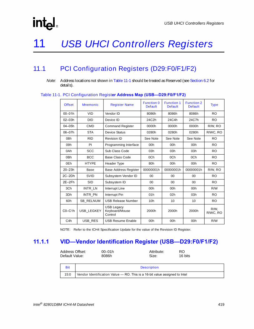
Intel® 82801DBM ICH4-M Datasheet 419
USB UHCI Controllers Registers
11 USB UHCI Controllers Registers
11.1 PCI Configuration Registers (D29:F0/F1/F2)Note: Address locations not shown in Table 11-1 should be treated as Reserved (see Section 6.2 for
details).
NOTE: Refer to the ICH4 Specification Update for the value of the Revision ID Register.
11.1.1 VID�Vendor Identification Register (USB�D29:F0/F1/F2)Address Offset: 00�01h Attribute: RODefault Value: 8086h Size: 16 bits
Table 11-1. PCI Configuration Register Address Map (USB�D29:F0/F1/F2)
Offset Mnemonic Register Name Function 0 Default
Function 1 Default
Function 2 Default Type
00�01h VID Vendor ID 8086h 8086h 8086h RO
02�03h DID Device ID 24C2h 24C4h 24C7h RO
04�05h CMD Command Register 0000h 0000h 0000h R/W, RO
06�07h STA Device Status 0280h 0280h 0280h R/WC, RO
08h RID Revision ID See Note See Note See Note RO
09h PI Programming Interface 00h 00h 00h RO
0Ah SCC Sub Class Code 03h 03h 03h RO
0Bh BCC Base Class Code 0Ch 0Ch 0Ch RO
0Eh HTYPE Header Type 80h 00h 00h RO
20�23h Base Base Address Register 00000001h 00000001h 00000001h R/W, RO
2C�2Dh SVID Subsystem Vendor ID 00 00 00 RO
2E�2Fh SID Subsystem ID 00 00 00 RO
3Ch INTR_LN Interrupt Line 00h 00h 00h R/W
3Dh INTR_PN Interrupt Pin 01h 02h 03h RO
60h SB_RELNUM USB Release Number 10h 10 10 RO
C0�C1h USB_LEGKEYUSB Legacy Keyboard/Mouse Control
2000h 2000h 2000h R/W, R/WC, RO
C4h USB_RES USB Resume Enable 00h 00h 00h R/W
Bit Description
15:0 Vendor Identification Value � RO. This is a 16-bit value assigned to Intel
420 Intel® 82801DBM ICH4-M Datasheet
USB UHCI Controllers Registers
11.1.2 DID�Device Identification Register (USB�D29:F0/F1/F2)Address Offset: 02�03h Attribute: RODefault Value: Function 0: 24C2h Size: 16 bits
Function 1: 24C4hFunction 2: 24C7h
11.1.3 CMD�Command Register (USB�D29:F0/F1/F2)Address Offset: 04�05h Attribute: R/W, RODefault Value: 0000h Size: 16 bits
Bit Description
15:0 Device Identification Value � RO. This is a 16-bit value assigned to the ICH4 USB Host Controllers.
Bit Description
15:10 Reserved
9 Fast Back to Back Enable (FBE) � RO. Reserved as 0.
8 SERR# Enable (SERR_EN) � RO. Reserved as 0.
7 Wait Cycle Control (WCC) � RO. Reserved as 0.
6 Parity Error Response (PER) � RO. Reserved as 0.
5 VGA Palette Snoop (VSP) � RO. Reserved as 0.
4 Postable Memory Write Enable (PMWE) � RO. Reserved as 0.
3 Special Cycle Enable (SCE) � RO. Reserved as 0.
2 Bus Master Enable (BME) � RW. When set, the ICH4 can act as a master on the PCI bus for USB transfers.
1 Memory Space Enable (MSE) � RO. Reserved as 0.
0
I/O Space Enable (IOSE) � RW. This bit controls access to the I/O space registers. 0 = Disable1 = Enable accesses to the USB I/O registers. The Base Address register for USB should be
programmed before this bit is set.

Intel® 82801DBM ICH4-M Datasheet 421
USB UHCI Controllers Registers
11.1.4 STA�Device Status Register (USB�D29:F0/F1/F2)Address Offset: 06�07h Attribute: R/WC, RODefault Value: 0280h Size: 16 bits
11.1.5 RID�Revision Identification Register (USB�D29:F0/F1/F2)Address Offset: 08h Attribute: RODefault Value: See Bit Description Size: 8 bits
11.1.6 PI�Programming Interface (USB�D29:F0/F1/F2)Address Offset: 09h Attribute: RODefault Value: 00h Size: 8 bits
Bit Description
15:14 Reserved as 00b. Read Only.
13Received Master Abort (RMA) � R/WC. 0 = Software clears this bit by writing a 1 to the bit location.1 = USB, as a master, generated a master-abort.
12 Reserved. Always read as 0.
11Signaled Target Abort (STA) � R/WC.0 = Software clears this bit by writing a 1 to the bit location.1 = USB function is targeted with a transaction that the ICH4 terminates with a target abort.
10:9DEVSEL# Timing Status (DEV_STS) � RO: This 2-bit field defines the timing for DEVSEL# assertion. These read only bits indicate the ICH4's DEVSEL# timing when performing a positive decode. ICH4 generates DEVSEL# with medium timing for USB.
8 Data Parity Error Detected (DPED) � RO. Reserved as 0.
7 Fast Back to Back Capable (FB2BC) � RO. Reserved as 1.
6 User Definable Features (UDF) � RO. Reserved as 0.
5 66 MHz Capable (66MHZ_CAP) � RO. Reserved as 0.
4:0 Reserved
Bit Description
7:0 Revision Identification Value � RO. Refer to the ICH4 Specification Update for the value of the Revision ID Register.
Bit Description
7:0Programming Interface � RO. 00h = No specific register level programming interface defined.

422 Intel® 82801DBM ICH4-M Datasheet
USB UHCI Controllers Registers
11.1.7 SCC�Sub Class Code Register (USB�D29:F0/F1/F2)Address Offset: 0Ah Attribute: RODefault Value: 03h Size: 8 bits
11.1.8 BCC�Base Class Code Register (USB�D29:F0/F1/F2)Address Offset: 0Bh Attribute: RODefault Value: 0Ch Size: 8 bits
11.1.9 HTYPE�Header Type Register (USB�D29:F0/F1/F2)Address Offset: 0Eh Attribute: RODefault Value: FN 0: 80h Size: 8 bits
FN 1: 00hFN 2: 00h
For functions 1 and 2, this register is hard-wired to 00h. For function 0, bit 7 is determined by the values in bits 15, 10, and 9 of the function disable register (D31:F0:F2h).
Bit Description
7:0Sub Class Code � RO. 03h = Universal Serial Bus Host Controller.
Bit Description
7:0Base Class Code � RO. 0Ch = Serial Bus Controller.
Bit Description
7
Multi-Function Bit � RO. When set to 1, this bit indicates to software that this is a multi-function device. A 0 indicates a single-function device. Since the upper functions in this device can be individually hidden, this bit must be based on the function-disable bits in Device 31, Function 0, Offset F2h as follows:D29:F7_Disable D29:F2_Disable D29:F1_Disable Multi-Function Bit (bit 15) (bit 10) (bit 9) 0 X X 1 X 0 X 1 X X 0 1 1 1 1 0
6:0 Header Type � RO. Hardwired to 00h, which indicates the standard PCI configuration layout.

Intel® 82801DBM ICH4-M Datasheet 423
USB UHCI Controllers Registers
11.1.10 BASE�Base Address Register (USB�D29:F0/F1/F2)Address Offset: 20�23h Attribute: R/W, RODefault Value: 00000001h Size: 32 bits
11.1.11 SVID � Subsystem Vendor ID (USB�D29:F0/F1/F2)Address Offset: 2Ch�2Dh Attribute: RODefault Value: 00h Size: 16 bitsLockable: No Power Well: Core
11.1.12 SID � Subsystem ID (USB�D29:F0/F1/F2)Address Offset: 2Eh�2Fh Attribute: RODefault Value: 00h Size: 16 bitsLockable: No Power Well: Core
Bit Description
31:16 Reserved
15:5 Base Address � R/W. Bits [15:5] correspond to I/O address signals AD [15:5], respectively. This gives 32 bytes of relocatable I/O space.
4:1 Reserved
0 Resource Type Indicator (RTE) � RO. This bit is hardwired to 1 indicating that the base address field in this register maps to I/O space
Bit Description
15:0 Subsystem Vendor ID (SVID) � RO. The SVID register, in combination with the Subsystem ID (SID) register, enables the operating system (OS) to distinguish subsystems from each other. The value returned by reads to this register is the same as what was written by BIOS into the IDE_SVID register.
Bit Description
15:0 Subsystem ID (SID) � R/Write-Once. The SID register, in combination with the SVID register, enables the operating system (OS) to distinguish subsystems from each other. The value returned by reads to this register is the same as what was written by BIOS into the IDE_SID register.

424 Intel® 82801DBM ICH4-M Datasheet
USB UHCI Controllers Registers
11.1.13 INTR_LN�Interrupt Line Register (USB�D29:F0/F1/F2)Address Offset: 3Ch Attribute: R/WDefault Value: 00h Size: 8 bits
11.1.14 INTR_PN�Interrupt Pin Register (USB�D29:F0/F1/F2)Address Offset: 3Dh Attribute: RODefault Value: Function 0: 01h Size: 8 bits
Function 1: 02hFunction 2: 03h
11.1.15 USB_RELNUM�USB Release Number Register (USB�D29:F0/F1/F2)Address Offset: 60h Attribute: RODefault Value: 10h Size: 8 bits
Bit Description
7:0 Interrupt Line (INT_LN) � R/W. This data is not used by the ICH4. It is to communicate to software the interrupt line that the interrupt pin is connected to.
Bit Description
7:3 Reserved
2:0
Interrupt Pin (INT_PN) � RO. The values of 01h, 02h, and 03h in function 0, 1, and 2, respectively, indicate to software that the corresponding ICH4 UHCI USB controllers drive the INTA#, INTB#, and INTC# PCI signals. Note that this does not determine the mapping to the ICH4 PIRQ inputs. Function 0 will drive PIRQA. Function 1 will drive PIRQD. Function 2 will drive PIRQC. Function 1 does not use the corresponding mapping in order to spread the interrupts with AC97, which has historically been mapped to PIRQB.
Bit Description
7:0USB Release Number � RO. 10h = Indicates that the USB controller is compliant with the USB specification, Release 1.0.

Intel® 82801DBM ICH4-M Datasheet 425
USB UHCI Controllers Registers
11.1.16 USB_LEGKEY�USB Legacy Keyboard/Mouse Control Register (USB�D29:F0/F1/F2)Address Offset: C0�C1h Attribute: R/W, R/WC, RODefault Value: 2000h Size: 16 bits
This register is implemented separately in each of the USB UHCI functions. However, the enable and status bits for the trapping logic are OR�d and shared, respectively, since their functionality is not specific to any one host controller.
Bit Description
15
SMI Caused by End of Pass-through (SMIBYENDPS) � R/WC. Indicates if the event occurred. Note that even if the corresponding enable bit is not set in bit 7, then this bit will still be active. It is up to the SMM code to use the enable bit to determine the exact cause of the SMI#. 0 = Software clears this bit by writing a 1 to the bit location in any of the controllers.1 = Event OccurredNOTE:This bit reports same value in all USB UHCI controllers.
14 Reserved
13
PCI Interrupt Enable (USBPIRQEN) � R/W. Used to prevent the USB controller from generating an interrupt due to transactions on its ports. Note, when disabled, that it will probably be configured to generate an SMI using bit 4 of this register. Default to 1 for compatibility with older USB software.0 = Disable1 = Enable
12
SMI Caused by USB Interrupt (SMIBYUSB) � RO. Indicates if an interrupt event occurred from this controller. The interrupt from the controller is taken before the enable in bit 13 has any effect to create this read-only bit. Note that even if the corresponding enable bit is not set in the Bit 4, then this bit may still be active. It is up to the SMM code to use the enable bit to determine the exact cause of the SMI#.0 = Software should clear the interrupts via the USB controllers. Writing a 1 to this bit will have no
effect. 1 = Event Occurred.
11
SMI Caused by Port 64 Write (TRAPBY64W) � R/WC. Indicates if the event occurred. Note that even if the corresponding enable bit is not set in the bit 3, then this bit will still be active. It is up to the SMM code to use the enable bit to determine the exact cause of the SMI#. Note that the A20Gate Pass-Through Logic allows specific port 64h writes to complete without setting this bit.0 = Software clears this bit by writing a 1 to the bit location in any of the controllers.1 = Event Occurred.NOTE: This bit reports same value in all USB UHCI controllers.
10
SMI Caused by Port 64 Read (TRAPBY64R) � R/WC. Indicates if the event occurred. Note that even if the corresponding enable bit is not set in the bit 2, then this bit will still be active. It is up to the SMM code to use the enable bit to determine the exact cause of the SMI#. 0 = Software clears this bit by writing a 1 to the bit location in any of the controllers.1 = Event Occurred.NOTE: This bit reports same value in all USB UHCI controllers.
9
SMI Caused by Port 60 Write (TRAPBY60W) � R/WC. Indicates if the event occurred. Note that even if the corresponding enable bit is not set in the bit 1, then this bit will still be active. It is up to the SMM code to use the enable bit to determine the exact cause of the SMI#. Note that the A20Gate Pass-Through Logic allows specific port 64h writes to complete without setting this bit.0 = Software clears this bit by writing a 1 to the bit location in any of the controllers.1 = Event Occurred.NOTE: This bit reports same value in all USB UHCI controllers.
426 Intel® 82801DBM ICH4-M Datasheet
USB UHCI Controllers Registers
11.1.17 USB_RES�USB Resume Enable Register (USB�D29:F0/F1/F2)Address Offset: C4h Attribute: R/WDefault Value: 00h Size: 8 bits
8
SMI Caused by Port 60 Read (TRAPBY60R) � R/WC. Indicates if the event occurred. Note that even if the corresponding enable bit is not set in the bit 0, then this bit will still be active. It is up to the SMM code to use the enable bit to determine the exact cause of the SMI#. 0 = Software clears this bit by writing a 1 to the bit location in any of the controllers.1 = Event Occurred.NOTE:This bit reports same value in all USB UHCI controllers.
7
SMI at End of Pass-through Enable (SMIATENDPS) � R/W. May need to cause SMI at the end of a pass-through. Can occur if an SMI is generated in the middle of a pass through, and needs to be serviced later.0 = Disable1 = EnableNOTE:Setting this bit in any controller enables the function.
6
Pass Through State (PSTATE) � RO.0 = If software needs to reset this bit, it should set bit 5 in all of the host controllers to 0.1 = Indicates that the state machine is in the middle of an A20GATE pass-through sequence.NOTE:This bit reports same value in all USB UHCI controllers.
5
A20Gate Pass-Through Enable (A20PASSEN) � R/W.0 = Disable.1 = Allows A20GATE sequence Pass-Through function. A specific cycle sequence involving writes to
port 60h and 64h does not result in the setting of the SMI status bits.NOTE:Setting this bit in any controller enables the function.
4SMI on USB IRQ Enable (USBSMIEN) � R/W.0 = Disable1 = USB interrupt will cause an SMI event.
3
SMI on Port 64 Writes Enable (64WEN) � R/W.0 = Disable1 = A 1 in bit 11 will cause an SMI event.NOTE:Setting this bit in any controller enables the function.
2
SMI on Port 64 Reads Enable (64REN) � R/W.0 = Disable1 = A 1 in bit 10 will cause an SMI event.NOTE:Setting this bit in any controller enables the function.
1
SMI on Port 60 Writes Enable (60WEN) � R/W.0 = Disable1 = A 1 in bit 9 will cause an SMI event.NOTE:Setting this bit in any controller enables the function.
0
SMI on Port 60 Reads Enable (60REN) � R/W.0 = Disable1 = A 1 in bit 8 will cause an SMI event.NOTE:Setting this bit in any controller enables the function.
Bit Description
Bit Description
7:2 Reserved

Intel® 82801DBM ICH4-M Datasheet 427
USB UHCI Controllers Registers
11.2 USB I/O RegistersSome of the read/write register bits which deal with changing the state of the USB hub ports function such that on read back they reflect the current state of the port, and not necessarily the state of the last write to the register. This allows the software to poll the state of the port and wait until it is in the proper state before proceeding. A Host Controller Reset, Global Reset, or Port Reset will immediately terminate a transfer on the affected ports and disable the port. This affects the USBCMD register, bit [4] and the PORTSC registers, bits [12, 6, 2]. See individual bit descriptions for more detail.
NOTES:1. These registers are Word writable only. Byte writes to these registers have unpredictable effects.
1PORT1EN � R/W. Enable port 1 of the USB controller to respond to wakeup events.0 = The USB controller will not look at this port for a wakeup event. 1 = The USB controller will monitor this port for remote wakeup and connect/disconnect events.
0PORT0EN � R/W. Enable port 0 of the USB controller to respond to wakeup events.0 = The USB controller will not look at this port for a wakeup event. 1 = The USB controller will monitor this port for remote wakeup and connect/disconnect events.
Table 11-2. USB I/O Registers
Offset Mnemonic Register Default Type
00�01h USBCMD USB Command 0000h R/W
02�03h USBSTS USB Status 0020h R/WC
04�05h USBINTR USB Interrupt Enable 0000h R/W
06�07h FRNUM USB Frame Number 0000h R/W (1)
08�0Bh FRBASEADD USB Frame List Base Address Undefined R/W
0Ch SOFMOD USB Start of Frame Modify 40h R/W
0D�0Fh Reserved 0 RO
10�11h PORTSC0 Port 0 Status/Control 0080h R/WC, R/W, RO (1)
12�13h PORTSC1 Port 1 Status/Control 0080h R/WC, R/W, RO (1)
14�17h Reserved 0 RO

428 Intel® 82801DBM ICH4-M Datasheet
USB UHCI Controllers Registers
11.2.1 USBCMD�USB Command RegisterI/O Offset: Base + (00�01h) Attribute: R/WDefault Value: 0000h Size: 16 bits
The Command Register indicates the command to be executed by the serial bus host controller. Writing to the register causes a command to be executed. The table following the bit description provides additional information on the operation of the Run/Stop and Debug bits.
Bit Description
15:7 Reserved
8
Loop Back Test Mode � R/W. 0 = Disable loop back test mode. 1 = ICH4 is in loop back test mode. When both ports are connected together, a write to one port will
be seen on the other port and the data will be stored in I/O offset 18h.
7
Max Packet (MAXP) � R/W. This bit selects the maximum packet size that can be used for full speed bandwidth reclamation at the end of a frame. This value is used by the Host Controller to determine whether it should initiate another transaction based on the time remaining in the SOF counter. Use of reclamation packets larger than the programmed size will cause a Babble error if executed during the critical window at frame end. The Babble error results in the offending endpoint being stalled. Software is responsible for ensuring that any packet which could be executed under bandwidth reclamation be within this size limit.0 = 32 bytes1 = 64 bytes
6
Configure Flag (CF) � R/W. This bit has no effect on the hardware. It is provided only as a semaphore service for software.0 = Indicates that software has not completed host controller configuration.1 = HCD software sets this bit as the last action in its process of configuring the Host Controller.
5
Software Debug (SWDBG) � R/W. The SWDBG bit must only be manipulated when the controller is in the stopped state. This can be determined by checking the HCHalted bit in the USBSTS register.0 = Normal Mode.1 = Debug mode. In SW Debug mode, the Host Controller clears the Run/Stop bit after the
completion of each USB transaction. The next transaction is executed when software sets the Run/Stop bit back to 1.
4
Force Global Resume (FGR) � R/W. 0 = Software resets this bit to 0 after 20 ms has elapsed to stop sending the Global Resume signal.
At that time all USB devices should be ready for bus activity. The 1-to-0 transition causes the port to send a low speed EOP signal. This bit will remain a 1 until the EOP has completed.
1 = Host Controller sends the Global Resume signal on the USB, and sets this bit to 1 when a resume event (connect, disconnect, or K-state) is detected while in global suspend mode.
3
Enter Global Suspend Mode (EGSM) � R/W. 0 = Software resets this bit to 0 to come out of Global Suspend mode. Software writes this bit to 0 at
the same time that Force Global Resume (bit 4) is written to 0 or after writing bit 4 to 0.1 = Host Controller enters the Global Suspend mode. No USB transactions occur during this time.
The Host Controller is able to receive resume signals from USB and interrupt the system. Software must ensure that the Run/Stop bit (bit 0) is cleared prior to setting this bit.
2
Global Reset (GRESET) � R/W. 0 = This bit is reset by the software after a minimum of 10 ms has elapsed as specified in Chapter 7
of the USB Specification.1 = Global Reset. The Host Controller sends the global reset signal on the USB and then resets all
its logic, including the internal hub registers. The hub registers are reset to their power on state. Chip Hardware Reset has the same effect as Global Reset (bit 2), except that the Host Controller does not send the Global Reset on USB.

Intel® 82801DBM ICH4-M Datasheet 429
USB UHCI Controllers Registers
When the USB Host Controller is in Software Debug Mode (USBCMD Register bit 5=1), the single-stepping software debug operation is as follows:
To Enter Software Debug Mode:
1. HCD puts Host Controller in Stop state by setting the Run/Stop bit to 0.
2. HCD puts Host Controller in Debug Mode by setting the SWDBG bit to 1.
1
Host Controller Reset (HCRESET) � R/W. The effects of HCRESET on Hub registers are slightly different from Chip Hardware Reset and Global USB Reset. The HCRESET affects bits [8,3:0] of the Port Status and Control Register (PORTSC) of each port. HCRESET resets the state machines of the Host Controller including the Connect/Disconnect state machine (one for each port). When the Connect/Disconnect state machine is reset, the output that signals connect/disconnect are negated to 0, effectively signaling a disconnect, even if a device is attached to the port. This virtual disconnect causes the port to be disabled. This disconnect and disabling of the port causes bit 1 (connect status change) and bit 3 (port enable/disable change) of the PORTSC to get set. The disconnect also causes bit 8 of PORTSC to reset. About 64 bit times after HCRESET goes to 0, the connect and low-speed detect will take place, and bits 0 and 8 of the PORTSC will change accordingly.0 = Reset by the Host Controller when the reset process is complete.1 = Reset. When this bit is set, the Host Controller module resets its internal timers, counters, state
machines, etc. to their initial value. Any transaction currently in progress on USB is immediately terminated.
0
Run/Stop (RS) � R/W. When set to 1, the ICH4 proceeds with execution of the schedule. The ICH4 continues execution as long as this bit is set. When this bit is cleared, the ICH4 completes the current transaction on the USB and then halts. The HC Halted bit in the status register indicates when the Host Controller has finished the transaction and has entered the stopped state. The Host Controller clears this bit when the following fatal errors occur: consistency check failure, PCI Bus errors.0 = Stop1 = Run
NOTE: This bit should only be cleared if there are no active Transaction Descriptors in the executable schedule or software will reset the host controller prior to setting this bit again.
Table 11-3. Run/Stop, Debug Bit Interaction SWDBG (Bit 5), Run/Stop (Bit 0) Operation
SWDBG (Bit 5)
Run/Stop(Bit 0) Description
0 0
If executing a command, the Host Controller completes the command and then stops. The 1.0 ms frame counter is reset and command list execution resumes from start of frame using the frame list pointer selected by the current value in the FRNUM register. (While Run/Stop=0, the FRNUM register can be reprogrammed).
0 1Execution of the command list resumes from Start Of Frame using the frame list pointer selected by the current value in the FRNUM register. The Host Controller remains running until the Run/Stop bit is cleared (by software or hardware).
1 0If executing a command, the Host Controller completes the command and then stops and the 1.0 ms frame counter is frozen at its current value. All status are preserved. The Host Controller begins execution of the command list from where it left off when the Run/Stop bit is set.
1 1
Execution of the command list resumes from where the previous execution stopped. The Run/Stop bit is set to 0 by the Host Controller when a TD is being fetched. This causes the Host Controller to stop again after the execution of the TD (single step). When the Host Controller has completed execution, the HC Halted bit in the Status Register is set.
Bit Description

430 Intel® 82801DBM ICH4-M Datasheet
USB UHCI Controllers Registers
3. HCD sets up the correct command list and Start Of Frame value for starting point in the Frame List Single Step Loop.
4. HCD sets Run/Stop bit to 1.
5. Host Controller executes next active TD, sets Run/Stop bit to 0, and stops.
6. HCD reads the USBCMD register to check if the single step execution is completed (HCHalted=1).
7. HCD checks results of TD execution. Go to step 4 to execute next TD or step 8 to end Software Debug mode.
8. HCD ends Software Debug mode by setting SWDBG bit to 0.
9. HCD sets up normal command list and Frame List table.
10. HCD sets Run/Stop bit to 1 to resume normal schedule execution.
In Software Debug mode, when the Run/Stop bit is set, the Host Controller starts. When a valid TD is found, the Run/Stop bit is reset. When the TD is finished, the HCHalted bit in the USBSTS register (bit 5) is set.
The SW Debug mode skips over inactive TDs and only halts after an active TD has been executed. When the last active TD in a frame has been executed, the Host Controller waits until the next SOF is sent and then fetches the first TD of the next frame before halting.
This HCHalted bit can also be used outside of Software Debug mode to indicate when the Host Controller has detected the Run/Stop bit and has completed the current transaction. Outside of the Software Debug mode, setting the Run/Stop bit to 0 always resets the SOF counter so that when the Run/Stop bit is set the Host Controller starts over again from the frame list location pointed to by the Frame List Index (see FRNUM Register description) rather than continuing where it stopped.

Intel® 82801DBM ICH4-M Datasheet 431
USB UHCI Controllers Registers
11.2.2 USBSTS�USB Status RegisterI/O Offset: Base + (02�03h) Attribute: R/WCDefault Value: 0020h Size: 16 bits
This register indicates pending interrupts and various states of the Host Controller. The status resulting from a transaction on the serial bus is not indicated in this register. Software sets a bit to 0 in this register by writing a 1 to it.
Bit Description
15:6 Reserved
5
HCHalted � R/WC.0 = Software resets this bit to 0 by writing a 1 to the bit position.1 = The Host Controller has stopped executing as a result of the Run/Stop bit being set to 0, either
by software or by the Host Controller hardware (debug mode or an internal error). Default.
4
Host Controller Process Error � R/WC. 0 = Software resets this bit to 0 by writing a 1 to the bit position.1 = The Host Controller has detected a fatal error. This indicates that the Host Controller suffered
a consistency check failure while processing a Transfer Descriptor. An example of a consistency check failure would be finding an illegal PID field while processing the packet header portion of the TD. When this error occurs, the Host Controller clears the Run/Stop bit in the Command register to prevent further schedule execution. A hardware interrupt is generated to the system.
3
Host System Error � R/WC.0 = Software resets this bit to 0 by writing a 1 to the bit position.1 = A serious error occurred during a host system access involving the Host Controller module. In
a PCI system, conditions that set this bit to 1 include PCI Parity error, PCI Master Abort, and PCI Target Abort. When this error occurs, the Host Controller clears the Run/Stop bit in the Command register to prevent further execution of the scheduled TDs. A hardware interrupt is generated to the system.
2
Resume Detect (RSM_DET) � R/WC.0 = Software resets this bit to 0 by writing a 1 to the bit position.1 = The Host Controller received a �RESUME� signal from a USB device. This is only valid if the
Host Controller is in a global suspend state (bit 3 of Command register = 1).
1
USB Error Interrupt � R/WC.0 = Software resets this bit to 0 by writing a 1 to the bit position.1 = Completion of a USB transaction resulted in an error condition (e.g., error counter underflow).
If the TD on which the error interrupt occurred also had its IOC bit set, both this bit and Bit 0 are set.
0
USB Interrupt (USBINT) � R/WC.0 = Software resets this bit to 0 by writing a 1 to the bit position.1 = The Host Controller sets this bit when the cause of an interrupt is a completion of a USB
transaction whose Transfer Descriptor had its IOC bit set. Also set when a short packet is detected (actual length field in TD is less than maximum length field in TD), and short packet detection is enabled in that TD.

432 Intel® 82801DBM ICH4-M Datasheet
USB UHCI Controllers Registers
11.2.3 USBINTR�Interrupt Enable RegisterI/O Offset: Base + (04�05h) Attribute: R/WDefault Value: 0000h Size: 16 bits
This register enables and disables reporting of the corresponding interrupt to the software. When a bit is set and the corresponding interrupt is active, an interrupt is generated to the host. Fatal errors (Host Controller Processor Error-bit 4, USBSTS Register) cannot be disabled by the host controller. Interrupt sources that are disabled in this register still appear in the Status Register to allow the software to poll for events.
11.2.4 FRNUM�Frame Number RegisterI/O Offset: Base + (06�07h) Attribute: R/W (Writes must be Word Writes)Default Value: 0000h Size: 16 bits
Bits [10:0] of this register contain the current frame number which is included in the frame SOF packet. This register reflects the count value of the internal frame number counter. Bits [9:0] are used to select a particular entry in the Frame List during scheduled execution. This register is updated at the end of each frame time.
This register must be written as a word. Byte writes are not supported. This register cannot be written unless the Host Controller is in the STOPPED state as indicated by the HCHalted bit (USBSTS register). A write to this register while the Run/Stop bit is set (USBCMD register) is ignored.
Bit Description
15:4 Reserved
3Short Packet Interrupt Enable � R/W.0 = Disabled.1 = Enabled.
2Interrupt On Complete (IOC) Enable � R/W.0 = Disabled.1 = Enabled.
1Resume Interrupt Enable � R/W.0 = Disabled.1 = Enabled.
0Timeout/CRC Interrupt Enable � R/W.0 = Disabled.1 = Enabled.
Bit Description
15:11 Reserved
10:0
Frame List Current Index/Frame Number � R/W. Provides the frame number in the SOF Frame. The value in this register increments at the end of each time frame (approximately every 1 ms). In addition, bits [9:0] are used for the Frame List current index and correspond to memory address signals [11:2].

Intel® 82801DBM ICH4-M Datasheet 433
USB UHCI Controllers Registers
11.2.5 FRBASEADD�Frame List Base AddressI/O Offset: Base + (08�0Bh) Attribute: R/WDefault Value: Undefined Size: 32 bits
This 32-bit register contains the beginning address of the Frame List in the system memory. HCD loads this register prior to starting the schedule execution by the Host Controller. When written, only the upper 20 bits are used. The lower 12 bits are written as 0s (4-kB alignment). The contents of this register are combined with the frame number counter to enable the Host Controller to step through the Frame List in sequence. The two least significant bits are always 00. This requires DWord alignment for all list entries. This configuration supports 1024 Frame List entries.
Bit Description
31:12 Base Address � R/W. These bits correspond to memory address signals [31:12], respectively.
11:0 Reserved

434 Intel® 82801DBM ICH4-M Datasheet
USB UHCI Controllers Registers
11.2.6 SOFMOD�Start of Frame Modify RegisterI/O Offset: Base + (0Ch) Attribute: R/WDefault Value: 40h Size: 8 bits
This 1-byte register is used to modify the value used in the generation of SOF timing on the USB. Only the 7 least significant bits are used. When a new value is written into these 7 bits, the SOF timing of the next frame will be adjusted. This feature can be used to adjust out any offset from the clock source that generates the clock that drives the SOF counter. This register can also be used to maintain real time synchronization with the rest of the system so that all devices have the same sense of real time. Using this register, the frame length can be adjusted across the full range required by the USB specification. Its initial programmed value is system dependent based on the accuracy of hardware USB clock and is initialized by system BIOS. It may be reprogrammed by USB system software at any time. Its value will take effect from the beginning of the next frame. This register is reset upon a Host Controller Reset or Global Reset. Software must maintain a copy of its value for reprogramming if necessary.
Bit Description
7 Reserved
6:0
SOF Timing Value � R/W. Guidelines for the modification of frame time are contained in Chapter 7 of the USB Specification. The SOF cycle time (number of SOF counter clock periods to generate a SOF frame length) is equal to 11936 + value in this field. The default value is decimal 64 which gives a SOF cycle time of 12000. For a 12-MHz SOF counter clock input, this produces a 1 ms Frame period. The following table indicates what SOF Timing Value to program into this field for a certain frame period.Frame Length(# 12 MHz Clocks)SOF Reg. Value (decimal) (decimal)
119360119371....119996312000641200165....1206212612063127
Intel® 82801DBM ICH4-M Datasheet 435
USB UHCI Controllers Registers
11.2.7 PORTSC[0,1]�Port Status and Control RegisterI/O Offset: Port 0/2/4: Base + (10�11h)Attribute: R/WC, RO, R/W (Word writes only)
Port 1/3/5: Base + (12�13h)Default Value: 0080h Size: 16 bits
Note: For Function 0, this register applies to ICH4 USB ports 0 and 1; for Function 1, this register applies to ICH4 USB ports 2 and 3; for Function 2, this register applies to ICH4 USB ports 4 and 5.
After a Power-up reset, Global reset, or Host Controller reset, the initial conditions of a port are: no device connected, port disabled, and the bus line status is 00 (single-ended zero).
Bit Description
15:13 Reserved � RO.
12
Suspend � R/W This bit should not be written to a 1 if global suspend is active (bit 3=1 in the USBCMD register). Bit 2 and bit 12 of this register define the hub states as follows:
Bits [12,2]Hub StateX0Disable01Enable11Suspend
When in suspend state, downstream propagation of data is blocked on this port, except for single-ended 0 resets (global reset and port reset). The blocking occurs at the end of the current transaction, if a transaction was in progress when this bit was written to 1. In the suspend state, the port is sensitive to resume detection. Note that the bit status does not change until the port is suspended and that there may be a delay in suspending a port if there is a transaction currently in progress on the USB.0 = Port not in suspend state. 1 = Port in suspend state.
NOTE: Normally, if a transaction is in progress when this bit is set, the port will be suspended when the current transaction completes. However, in the case of a specific error condition (out transaction with babble), the ICH4 may issue a start-of-frame, and then suspend the port.
11Over-current Indicator � R/WC. Set by hardware.0 = Software clears this bit by writing a 1 to the bit position.1 = Overcurrent pin has gone from inactive to active on this port.
10Over-current Active � RO. This bit is set and cleared by hardware. 0 = Indicates that the overcurrent pin is inactive (high).1 = Indicates that the overcurrent pin is active (low).
9Port Reset � R/W0 = Port is not in Reset.1 = Port is in Reset. When set, the port is disabled and sends the USB Reset signaling.
8Low Speed Device Attached (LS) � RO Writes have no effect.0 = Full speed device is attached.1 = Low speed device is attached to this port.
7 Reserved � RO. Always read as 1.
6
Resume Detect (RSM_DET) � R/W. Software sets this bit to a 1 to drive resume signaling. The Host Controller sets this bit to a 1 if a J-to-K transition is detected for at least 32 microseconds while the port is in the Suspend state. The ICH4 will then reflect the K-state back onto the bus as long as the bit remains a 1, and the port is still in the suspend state (bit 12,2 are 11). Writing a 0 (from 1) causes the port to send a low speed EOP. This bit will remain a 1 until the EOP has completed.0 = No resume (K-state) detected/driven on port.1 = Resume detected/driven on port.

436 Intel® 82801DBM ICH4-M Datasheet
USB UHCI Controllers Registers
5:4Line Status � RO These bits reflect the D+ (bit 4) and D- (bit 5) signals line�s logical levels. These bits are used for fault detect and recovery as well as for USB diagnostics. This field is updated at EOF2 time (See Chapter 11 of the USB Specification).
3
Port Enable/Disable Change � R/WC For the root hub, this bit gets set only when a port is disabled due to disconnect on that port or due to the appropriate conditions existing at the EOF2 point (See Chapter 11 of the USB Specification).0 = No change. Software clears this bit by writing a 1 to the bit location.1 = Port enabled/disabled status has changed.
2
Port Enabled/Disabled (PORT_EN) � R/W Ports can be enabled by host software only. Ports can be disabled by either a fault condition (disconnect event or other fault condition) or by host software. Note that the bit status does not change until the port state actually changes and that there may be a delay in disabling or enabling a port if there is a transaction currently in progress on the USB.0 = Disable1 = Enable
1
Connect Status Change � R/WC Indicates that a change has occurred in the port�s Current Connect Status (see bit 0). The hub device sets this bit for any changes to the port device connect status, even if system software has not cleared a connect status change. If, for example, the insertion status changes twice before system software has cleared the changed condition, hub hardware will be setting� an already-set bit (i.e., the bit will remain set). However, the hub transfers the change bit only once when the Host Controller requests a data transfer to the Status Change endpoint. System software is responsible for determining state change history in such a case.0 = No change. Software clears this bit by writing a 1 to the bit location.1 = Change in Current Connect Status.
0
Current Connect Status � RO This value reflects the current state of the port, and may not correspond directly to the event that caused the Connect Status Change bit (Bit 1) to be set.0 = No device is present.1 = Device is present on port.
Bit Description

Intel® 82801DBM ICH4-M Datasheet 437
EHCI Controller Registers (D29:F7)
12 EHCI Controller Registers (D29:F7)
12.1 USB EHCI Configuration Registers (D29:F7)Note: Register address locations not shown in Table 12-1 should be treated as Reserved (see Section 6.2
for details).
Table 12-1. USB EHCI PCI Configuration Register Address Map (D29:F7) (Sheet 1 of 2)
Offset Mnemonic Register Name Default Value Type
00�01h VID Vendor ID 8086h RO
02�03h DID Device ID 24CDh RO
04�05h PCICMD Command Register 0000h R/W, RO
06�07h PCISTS Device Status 0290h R/WC, RO
08h REVID Revision ID See Note RO
09h PI Programming Interface 20h RO
0Ah SCC Sub Class Code 03h RO
0Bh BCC Base Class Code 0Ch RO
0Dh MLT Master Latency Timer 00h RO
10�13h MEM_BASE Memory Base Address Register 00000000h R/W, RO
2C�2Dh SVID Subsystem Vendor ID XXXXh R/W-Special
2E�2Fh SID Subsystem ID XXXXh R/W-Special
34h CAP_PTR Capabilities Pointer 50h
3Ch INT_LN Interrupt Line 00h R/W
3Dh INT_PN Interrupt Pin 04h RO
50h PWR_CAPID Power Management Capability ID 01h RO
51h NXT_PRT1 Next Item Pointer #1 58h R/W-Special
52�53h PWR_CAP Power Management Capabilities C9C2h R/W-Special
54�55h PWR_CNTL_STS Power Management Control/Status 0000h R/W, R/WC
58h DEBUG_CAPID Debug Port Capability ID 0Ah RO
59h NXT_PRT2 Next Item Pointer #2 00h RO
5A�5Bh DEBUG_BASE Debug Port Base Offset 2080h RO
60h USB_RELNUM USB Release Number 20h RO
61h FL_ADJ Frame Length Adjustment 20h R/W
62�63h PWAKE_CAP Power Wake Capabilities 007Fh R/W
64�65h PORT_OVRIDE USB UHCI Port Override 0000 R/W
66�67h Reserved 0 RO
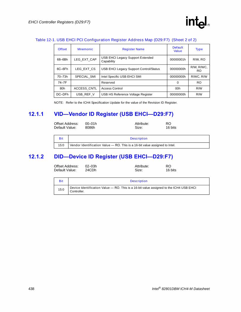
438 Intel® 82801DBM ICH4-M Datasheet
EHCI Controller Registers (D29:F7)
NOTE: Refer to the ICH4 Specification Update for the value of the Revision ID Register.
12.1.1 VID�Vendor ID Register (USB EHCI�D29:F7)Offset Address: 00�01h Attribute: RODefault Value: 8086h Size: 16 bits
12.1.2 DID�Device ID Register (USB EHCI�D29:F7)Offset Address: 02�03h Attribute: RODefault Value: 24CDh Size: 16 bits
68�6Bh LEG_EXT_CAP USB EHCI Legacy Support Extended Capability 00000001h R/W, RO
6C�6Fh LEG_EXT_CS USB EHCI Legacy Support Control/Status 00000000h R/W, R/WC, RO
70�73h SPECIAL_SMI Intel Specific USB EHCI SMI 00000000h R/WC, R/W
74�7F Reserved 0 RO
80h ACCESS_CNTL Access Control 00h R/W
DC�DFh USB_REF_V USB HS Reference Voltage Register 00000000h R/W
Table 12-1. USB EHCI PCI Configuration Register Address Map (D29:F7) (Sheet 2 of 2)
Offset Mnemonic Register Name Default Value Type
Bit Description
15:0 Vendor Identification Value � RO. This is a 16-bit value assigned to Intel.
Bit Description
15:0 Device Identification Value � RO. This is a 16-bit value assigned to the ICH4 USB EHCI Controller.

Intel® 82801DBM ICH4-M Datasheet 439
EHCI Controller Registers (D29:F7)
12.1.3 PCICMD�PCI Command Register (USB EHCI�D29:F7)Address Offset: 04�05h Attribute: R/W, RODefault Value: 0000h Size: 16 bits
Bit Description
15:10 Reserved
9 Fast Back to Back Enable (FBE) � RO. Reserved as 0.
8
SERR# Enable (SERR_EN) � R/W.0 = Disables EHC�s capability to generate an SERR#.1 = The Enhanced Host Controller (EHC) is capable of generating (internally) SERR# when it
receive a completion status other than �successful� for one of its DMA-initiated memory reads on the hub interface (and subsequently on its internal interface).
7 Wait Cycle Control (WCC) � RO. Reserved as 0.
6 Parity Error Response (PER) � RO. Reserved as 0.
5 VGA Palette Snoop (VPS) � RO. Reserved as 0.
4 Postable Memory Write Enable (PMWE) � RO. Reserved as 0.
3 Special Cycle Enable (SCE) � RO. Reserved as 0.
2Bus Master Enable (BME) � R/W.0 = Disables this functionality.1 = Enables the ICH4 can act as a master on the PCI bus for USB transfers.
1
Memory Space Enable (MSE) � R/W. This bit controls access to the USB EHCI Memory Space registers. 0 = Disables this functionality.1 = Enables accesses to the USB EHCI registers. The Base Address register for USB EHCI should
be programmed before this bit is set.
0 I/O Space Enable (IOSE) � RO. Reserved as 0.

440 Intel® 82801DBM ICH4-M Datasheet
EHCI Controller Registers (D29:F7)
12.1.4 PCISTS�PCI Device Status Register (USB EHCI�D29:F7)Address Offset: 06�07h Attribute: R/WC, RODefault Value: 0290h Size: 16 bits
12.1.5 REVID�Revision ID Register (USB EHCI�D29:F7)Offset Address: 08h Attribute: RODefault Value: See Bit Description Size: 8 bits
Bit Description
15 Detected Parity Error (DPE) � RO. Reserved as 0.
14
Signaled System Error (SSE) � R/WC. 0 = Software clears this bit by writing a 1 to this bit location.1 = ICH4 signaled SERR# (internally). The SER_EN bit (bit 8 of the Command Register) must be 1
for this bit to be set.
13
Received Master Abort (RMA) � R/WC.0 = Software clears this bit by writing a 1 to this bit location.1 = USB EHCI, as a master, received a master abort status on a memory access. This is treated as
a Host Error and halts the DMA engines. This event can optionally generate an SERR# by setting the SERR# Enable bit.
12
Received Target Abort (RTA) � R/WC.0 = Software clears this bit by writing a 1 to this bit location.1 = USB EHCI, as a master, received a target abort status on a memory access. This is treated as
a Host Error and halts the DMA engines. This event can optionally generate an SERR# by setting the SERR# Enable bit.
11Signaled Target Abort (STA) � RO. Hardwired to 0. This bit is used to indicate when the USB EHCI function responds to a cycle with a target abort. There is no reason for this to happen; thus, this bit is hardwired to 0.
10:9 DEVSEL# Timing Status (DEV_STS) � RO. This 2-bit field defines the timing for DEVSEL# assertion.
8
Master Data Parity Error Detected (DPED) � R/WC. 0 = Software clears this bit by writing a 1 to this bit location.1 = ICH4 detected a data parity error on a USB EHCI read completion packet on the internal
interface to the USB EHCI host controller (due to an equivalent data parity error on hub interface), and bit 6 of the Command register is set to 1.
7 Fast Back to Back Capable (FB2BC) � RO. Reserved as 1.
6 User Definable Features (UDF) � RO. Reserved as 0.
5 66 MHz Capable (66MHZ_CAP) � RO. Reserved as 0.
4 Capabilities List (CAP_LIST) � RO. This bit is hardwired to 1 indicating the presence of a valid capabilities pointer at offset 34h.
3:0 Reserved.
Bit Description
7:0 Revision Identification Value � RO. Refer to the ICH4 Specification Update for the value of the Revision ID Register.

Intel® 82801DBM ICH4-M Datasheet 441
EHCI Controller Registers (D29:F7)
12.1.6 PI�Programming Interface Register (USB EHCI�D29:F7)Address Offset: 09h Attribute: RODefault Value: 20h Size: 8 bits
12.1.7 SCC�Sub Class Code Register (USB EHCI�D29:F7)Address Offset: 0Ah Attribute: RODefault Value: 03h Size: 8 bits
12.1.8 BCC�Base Class Code Register (USB EHCI�D29:F7)Address Offset: 0Bh Attribute: RODefault Value: 0Ch Size: 8 bits
12.1.9 MLT� PCI Master Latency Timer Register (USB EHCI�D29:F7)Address Offset: 0Dh Attribute: RODefault Value: 00h Size: 8 bits
Bit Description
7:0 Programming Interface � RO. A value of 20h indicates that this USB High-speed Host Controller conforms to the EHCI Specification.
Bit Description
7:0 Sub Class Code � RO. A value of 03h indicates that this is a Universal Serial Bus Host Controller.
Bit Description
7:0 Base Class Code � RO. A value of 0Ch indicates that this is a Serial Bus controller.
Bit Description
7:0 Master Latency Timer Count (MLTC) � RO. Hardwired to 00h. Because the USB EHCI controller is internally implemented with arbitration via hub interface (and not PCI), it does not need a master latency timer.

442 Intel® 82801DBM ICH4-M Datasheet
EHCI Controller Registers (D29:F7)
12.1.10 MEM_BASE�Memory Base Address Register (USB EHCI�D29:F7)Address Offset: 10�13h Attribute: R/W, RODefault Value: 00000000h Size: 32 bits
12.1.11 SVID�USB EHCI Subsystem Vendor ID Register (USB EHCI�D29:F7)Address Offset: 2C�2Dh Attribute: R/W-SpecialDefault Value: XXXXh Size: 16 bitsReset: None
12.1.12 SID�USB EHCI Subsystem ID Register (USB EHCI�D29:F7)Address Offset: 2E�2Fh Attribute: R/W-Special Default Value: XXXXh Size: 16 bitsReset: None
Bit Description
31:10 Base Address � R/W. Bits [31:10] correspond to memory address signals [31:10], respectively. This provides 1 kB of locatable memory space aligned to 1-kB boundaries.
9:4 Reserved
3 Prefetchable � RO. Hardwired to 0; indicates that this range should not be prefetched.
2:1 Type � RO. Hardwired to 00b; indicates that this range can be mapped anywhere within 32-bit address space.
0 Resource Type Indicator (RTE) � RO. Hardwired to 0; indicates that the base address field in this register maps to memory space.
Bit Description
15:0Subsystem Vendor ID (SVID) � R/W-Special. This register, in combination with the USB EHCI Subsystem ID register, enables the operating system to distinguish each subsystem from the others.NOTE: Writes to this register are enabled when the WRT_RDONLY bit (offset 80h, bit 0) is set to 1.
Bit Description
15:0
Subsystem ID (SID) � R/W-Special. BIOS sets the value in this register to identify the Subsystem ID. This register, in combination with the Subsystem Vendor ID register, enables the operating system to distinguish each subsystem from other(s).NOTE: Writes to this register are enabled when the WRT_RDONLY bit (offset 80h, bit 0) is set to 1.

Intel® 82801DBM ICH4-M Datasheet 443
EHCI Controller Registers (D29:F7)
12.1.13 CAP_PTR�Capabilities Pointer Register (USB EHCI�D29:F7)Address Offset: 34h Attribute: RO Default Value: 50h Size: 8 bits
12.1.14 INT_LN�Interrupt Line Register (USB EHCI�D29:F7)Address Offset: 3Ch Attribute: R/WDefault Value: 00h Size: 8 bits
12.1.15 INT_PN�Interrupt Pin Register (USB EHCI�D29:F7)Address Offset: 3Dh Attribute: RODefault Value: 04h Size: 8 bits
12.1.16 PWR_CAPID�PCI Power Management Capability ID Register (USB EHCI�D29:F7)Address Offset: 50h Attribute: RODefault Value: 01h Size: 8 bits
Bit Description
7: 0 Capabilities Pointer (CAP_PTR) � RO. This register points to the starting offset of the USB EHCI capabilities ranges.
Bit Description
7:0 Interrupt Line (INT_LN) � R/W. This data is not used by the ICH4. It is used as a scratchpad register to communicate to software the interrupt line that the interrupt pin is connected to.
Bit Description
7:0
Interrupt Pin (INT_PN) � RO. The value of 04h indicates that the USB EHCI function within the ICH4�s multi-function USB device will drive the fourth interrupt pin from the device (INTD# in PCI terms). The value of 04h in function 7 is required because the PCI specification does not recognize more than 4 interrupts and older APM-based OSs require that each function within a multi-function device has a different Interrupt Pin Register value.NOTE: Internally the USB EHCI controller uses PIRQ[H]#.
Bit Description
7:0 Power Management Capability ID � RO. A value of 01h indicates that this is a PCI Power Management capabilities field.

444 Intel® 82801DBM ICH4-M Datasheet
EHCI Controller Registers (D29:F7)
12.1.17 NXT_PTR1�Next Item Pointer #1 Register (USB EHCI�D29:F7)Address Offset: 51h Attribute: R/W-SpecialDefault Value: 58h Size: 8 bits
12.1.18 PWR_CAP�Power Management Capabilities Register (USB EHCI�D29:F7)Address Offset: 52�53h Attribute: R/W-SpecialDefault Value: C9C2h Size: 16 bits
NOTES:1. Normally, this register is read-only to report capabilities to the power management software. To report
different power management capabilities, depending on the system in which the ICH4ICH4 is used, bits 15:11 and 8:6 in this register are writable when the WRT_RDONLY bit is set. The value written to this register does not affect the hardware other than changing the value returned during a read.
2. Reset: core well, but not D3-to-D0 warm reset.
Bit Description
7:0
Next Item Pointer #1 Value � R/W-Special. This register defaults to 58h, which indicates that the next capability registers begin at configuration offset 58h. This register is writable when the WRT_RDONLY bit is set. This allows BIOS to effectively hide the Debug Port capability registers, if necessary. This register should only be written during system initialization before the plug-and-play software has enabled any master-initiated traffic. Only values of 58h (Debug Port visible) and 00h (Debug Port invisible) are expected to be programmed in this register.
Bit Description
15:11PME Support � R/W-Special. This 5-bit field indicates the power states in which the function may assert PME#. The ICH4 EHC does not support the D1 or D2 states. For all other states, the ICH4 EHC is capable of generating PME#. Software should never need to modify this field.
10D2 Support � R/W-Special. 0 = D2 State is not supported1 = D2 State is supported
9D1 Support � R/W-Special. 0 = D1 State is not supported1 = D1 State is supported
8:6Auxiliary Current � R/W-Special. The ICH4 EHC reports 375 mA maximum Suspend well current required when in the D3cold state. This value can be written by BIOS when a more accurate value is known.
5 DSI � R/W-Special. The ICH4 reports 0, indicating that no device-specific initialization is required.
4 Reserved
3 PME Clock � R/W-Special. The ICH4 reports 0, indicating that no PCI clock is required to generate PME#.
2:0 Version � R/W-Special. The ICH4 reports 010b, indicating that it complies with Revision 1.1 of the PCI Power Management Specification.

Intel® 82801DBM ICH4-M Datasheet 445
EHCI Controller Registers (D29:F7)
12.1.19 PWR_CNTL_STS�Power Management Control/Status Register (USB EHCI�D29:F7)Address Offset: 54�55h Attribute: R/WC, R/WDefault Value: 0000h Size: 16 bits
NOTE: Reset (bits 15, 8): suspend well, and not D3-to-D0 warm reset nor core well reset.
12.1.20 DEBUG_CAPID�Debug Port Capability ID Register (USB EHCI�D29:F7)Address Offset: 58h Attribute: RODefault Value: 0Ah Size: 8 bits
Bit Description
15
PME Status � R/WC. 0 = Writing a 1 to this bit clears it and causes the internal PME to deassert (if enabled). Writing a 0
has no effect. 1 = This bit is set when the ICH4 EHC would normally assert the PME# signal independent of the
state of the PME_En bit. NOTE: This bit must be explicitly cleared by the operating system each time the operating system
is loaded.
14:13 Data Scale � RO. Hardwired to 00b; ICH4 does not support the associated Data register.
12:9 Data Select � RO. Hardwired to 0000b; ICH4 does not support the associated Data register.
8
PME Enable � R/W. 0 = Disable.1 = Enables the ICH4 EHC to generate an internal PME signal when PME_Status is 1. NOTE: This bit must be explicitly cleared by the operating system each time it is initially loaded.
7:2 Reserved
1:0
Power State � R/W. This 2-bit field is used both to determine the current power state of EHC function and to set a new power state. The definition of the field values are: 00 = D0 state11 = D3 hot stateIf software attempts to write a value of 10b or 01b in to this field, the write operation must complete normally; however, the data is discarded and no state change occurs. When in the D3 hot state, the ICH4 must not accept accesses to the EHC memory range; but the configuration space must still be accessible. When not in the D0 state, the generation of the interrupt output is blocked. Specifically, the PIRQ[H] is not asserted by the ICH4 when not in the D0 state.When software changes this value from the D3 hot state to the D0 state, an internal warm (soft) reset is generated, and software must re-initialize the function.
Bit Description
7:0 Debug Port Capability ID � RO. Hardwired to 0Ah; indicates that this is the start of a Debug Port Capability structure.

446 Intel® 82801DBM ICH4-M Datasheet
EHCI Controller Registers (D29:F7)
12.1.21 NXT_PTR2�Next Item Pointer #2 Register (USB EHCI�D29:F7)Address Offset: 59h Attribute: RODefault Value: 00h Size: 8 bits
12.1.22 DEBUG_BASE�Debug Port Base Offset Register (USB EHCI�D29:F7)Address Offset: 5Ah�5Bh Attribute: RODefault Value: 2080h Size: 16 bits
12.1.23 USB_RELNUM�USB Release Number Register (USB EHCI�D29:F7)Address Offset: 60h Attribute: RODefault Value: 20h Size: 8 bits
Bit Description
7:0 Next Item Pointer 2 Capability � RO. Hardwired to 00h: indicates that there are no more capability structures in this function.
Bit Description
15:13 BAR Number � RO. Hardwired to 001b: indicates the memory BAR begins at offset 10h in the EHCI configuration space.
12:0 Debug Port Offset � RO. Hardwired to 080h; indicates that the Debug Port registers begin at offset 80h in the EHCI memory range.
Bit Description
7:0 USB Release Number � RO. A value of 20h indicates that this controller follows the Universal Serial Bus (USB) Specification, Revision 2.0 .
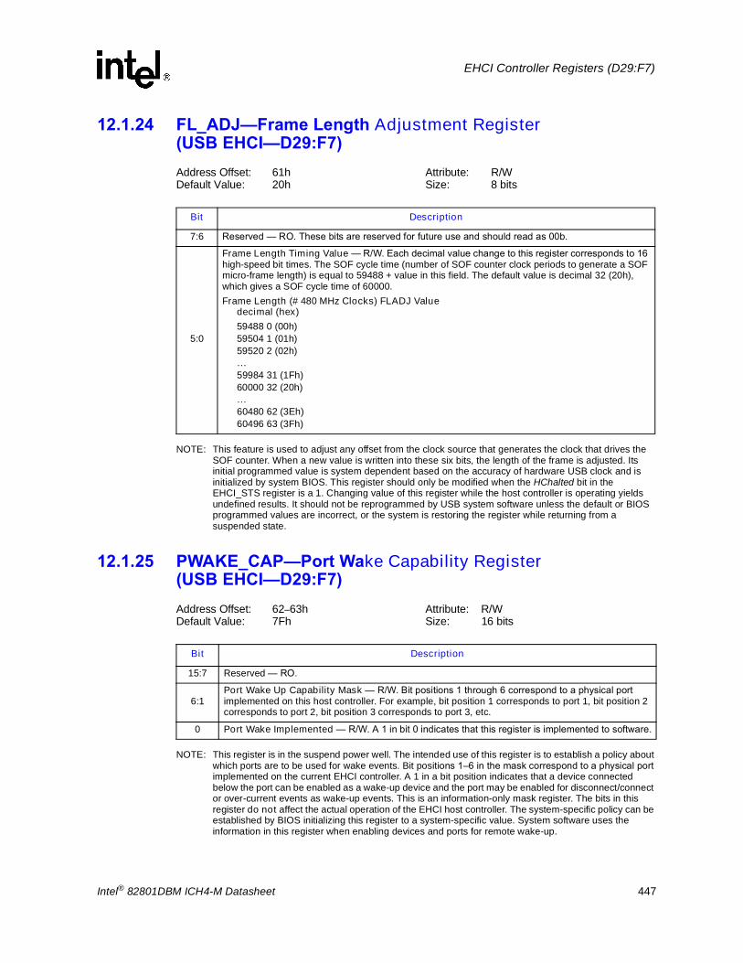
Intel® 82801DBM ICH4-M Datasheet 447
EHCI Controller Registers (D29:F7)
12.1.24 FL_ADJ�Frame Length Adjustment Register (USB EHCI�D29:F7)Address Offset: 61h Attribute: R/WDefault Value: 20h Size: 8 bits
NOTE: This feature is used to adjust any offset from the clock source that generates the clock that drives the SOF counter. When a new value is written into these six bits, the length of the frame is adjusted. Its initial programmed value is system dependent based on the accuracy of hardware USB clock and is initialized by system BIOS. This register should only be modified when the HChalted bit in the EHCI_STS register is a 1. Changing value of this register while the host controller is operating yields undefined results. It should not be reprogrammed by USB system software unless the default or BIOS programmed values are incorrect, or the system is restoring the register while returning from a suspended state.
12.1.25 PWAKE_CAP�Port Wake Capability Register (USB EHCI�D29:F7)Address Offset: 62�63h Attribute: R/WDefault Value: 7Fh Size: 16 bits
NOTE: This register is in the suspend power well. The intended use of this register is to establish a policy about which ports are to be used for wake events. Bit positions 1�6 in the mask correspond to a physical port implemented on the current EHCI controller. A 1 in a bit position indicates that a device connected below the port can be enabled as a wake-up device and the port may be enabled for disconnect/connect or over-current events as wake-up events. This is an information-only mask register. The bits in this register do not affect the actual operation of the EHCI host controller. The system-specific policy can be established by BIOS initializing this register to a system-specific value. System software uses the information in this register when enabling devices and ports for remote wake-up.
Bit Description
7:6 Reserved � RO. These bits are reserved for future use and should read as 00b.
5:0
Frame Length Timing Value � R/W. Each decimal value change to this register corresponds to 16 high-speed bit times. The SOF cycle time (number of SOF counter clock periods to generate a SOF micro-frame length) is equal to 59488 + value in this field. The default value is decimal 32 (20h), which gives a SOF cycle time of 60000.Frame Length (# 480 MHz Clocks) FLADJ Value
decimal (hex)59488 0 (00h)59504 1 (01h)59520 2 (02h)� 59984 31 (1Fh)60000 32 (20h)�60480 62 (3Eh)60496 63 (3Fh)
Bit Description
15:7 Reserved � RO.
6:1Port Wake Up Capability Mask � R/W. Bit positions 1 through 6 correspond to a physical port implemented on this host controller. For example, bit position 1 corresponds to port 1, bit position 2 corresponds to port 2, bit position 3 corresponds to port 3, etc.
0 Port Wake Implemented � R/W. A 1 in bit 0 indicates that this register is implemented to software.
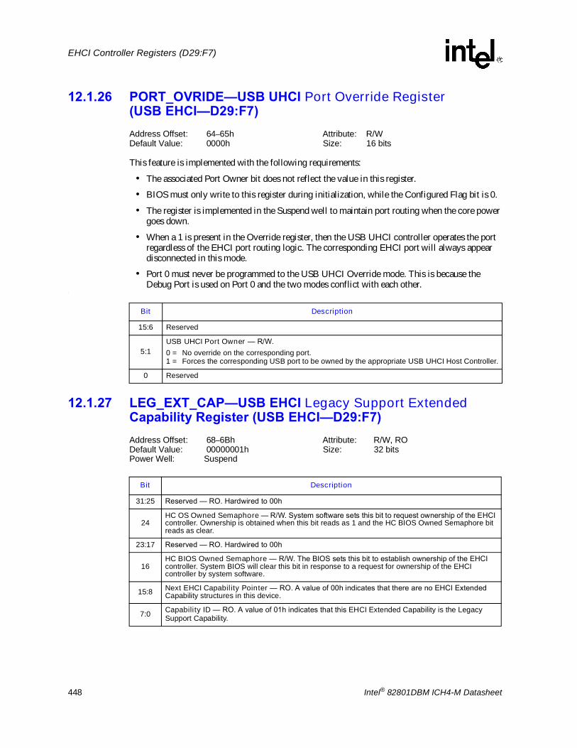
448 Intel® 82801DBM ICH4-M Datasheet
EHCI Controller Registers (D29:F7)
12.1.26 PORT_OVRIDE�USB UHCI Port Override Register (USB EHCI�D29:F7)Address Offset: 64�65h Attribute: R/WDefault Value: 0000h Size: 16 bits
This feature is implemented with the following requirements:
� The associated Port Owner bit does not reflect the value in this register.
� BIOS must only write to this register during initialization, while the Configured Flag bit is 0.
� The register is implemented in the Suspend well to maintain port routing when the core power goes down.
� When a 1 is present in the Override register, then the USB UHCI controller operates the port regardless of the EHCI port routing logic. The corresponding EHCI port will always appear disconnected in this mode.
� Port 0 must never be programmed to the USB UHCI Override mode. This is because the Debug Port is used on Port 0 and the two modes conflict with each other.
:
12.1.27 LEG_EXT_CAP�USB EHCI Legacy Support Extended Capability Register (USB EHCI�D29:F7)Address Offset: 68�6Bh Attribute: R/W, RODefault Value: 00000001h Size: 32 bitsPower Well: Suspend
Bit Description
15:6 Reserved
5:1USB UHCI Port Owner � R/W.0 = No override on the corresponding port.1 = Forces the corresponding USB port to be owned by the appropriate USB UHCI Host Controller.
0 Reserved
Bit Description
31:25 Reserved � RO. Hardwired to 00h
24HC OS Owned Semaphore � R/W. System software sets this bit to request ownership of the EHCI controller. Ownership is obtained when this bit reads as 1 and the HC BIOS Owned Semaphore bit reads as clear.
23:17 Reserved � RO. Hardwired to 00h
16HC BIOS Owned Semaphore � R/W. The BIOS sets this bit to establish ownership of the EHCI controller. System BIOS will clear this bit in response to a request for ownership of the EHCI controller by system software.
15:8 Next EHCI Capability Pointer � RO. A value of 00h indicates that there are no EHCI Extended Capability structures in this device.
7:0 Capability ID � RO. A value of 01h indicates that this EHCI Extended Capability is the Legacy Support Capability.

Intel® 82801DBM ICH4-M Datasheet 449
EHCI Controller Registers (D29:F7)
12.1.28 LEG_EXT_CS�USB EHCI Legacy Support Extended Control / Status Register (USB EHCI�D29:F7)Address Offset: 6C�6Fh Attribute: R/W, R/WC, RODefault Value: 00000000h Size: 32 bitsPower Well: Suspend
Bit Description
31SMI on BAR�R/WC. 0 = Software clears this bit by writing a 1 to this bit location.1 = This bit is set to 1 whenever the Base Address Register (BAR) is written.
30SMI on PCI Command � R/WC. 0 = Software clears this bit by writing a 1 to this bit location.1 = This bit is set to 1 whenever the PCI Command Register is written.
29
SMI on OS Ownership Change � R/WC. 0 = Software clears this bit by writing a 1 to this bit location.1 = HC OS Owned Semaphore bit in the USB EHCI Legacy Support Extended Capability register
transitioned from 1-to-0 or 0-to-1.
28:22 Reserved � RO. Hardwired to 00h
21SMI on Async Advance � RO. Shadow bit of the Interrupt on Async Advance bit in the EHCI_STS register. NOTE: To clear this bit system software must write a 1 to the Interrupt on Async Advance bit in the
EHCI_STS register.
20SMI on Host System Error � RO. Shadow bit of Host System Error bit in the EHCI_STS register. NOTE: To clear this bit system software must write a 1 to the Host System Error bit in the
EHCI_STS register.
19SMI on Frame List Rollover � RO. Shadow bit of Frame List Rollover bit in the EHCI_STS register. NOTE: To clear this bit system software must write a 1 to the Frame List Rollover bit in the
EHCI_STS register.
18SMI on Port Change Detect � RO. Shadow bit of Port Change Detect bit in the EHCI_STS register. NOTE: To clear this bit system software must write a 1 to the Port Change Detect bit in the
EHCI_STS register.
17SMI on USB Error � RO. Shadow bit of USB Error Interrupt (USBERRINT) bit in the EHCI_STS register. NOTE: To clear this bit system software must write a 1 to the USB Error Interrupt bit in the
EHCI_STS register.
16SMI on USB Complete � RO. Shadow bit of USB Interrupt (USBINT) bit in the EHCI_STS register. NOTE: To clear this bit system software must write a 1 to the USB Interrupt bit in the EHCI_STS
register.
15SMI on BAR Enable � R/W. 0 = Disable. 1 = Enable. When this bit is 1 and SMI on BAR is 1, then the host controller will issue an SMI.
14
SMI on PCI Command Enable � R/W. 0 = Disable. 1 = Enable. When this bit is 1 and SMI on PCI Command is 1, then the host controller will issue an
SMI.
13
SMI on OS Ownership Enable � R/W. 0 = Disable. 1 = Enable. When this bit is a 1 AND the OS Ownership Change bit is 1, the host controller will
issue an SMI.
12:6 Reserved � RO. Hardwired to 00h

450 Intel® 82801DBM ICH4-M Datasheet
EHCI Controller Registers (D29:F7)
5
SMI on Async Advance Enable � R/W. 0 = Disable. 1 = Enable. When this bit is a 1, and the SMI on Async Advance bit is a 1, the host controller will
issue an SMI immediately.
4
SMI on Host System Error Enable � R/W. 0 = Disable. 1 = Enable. When this bit is a 1, and the SMI on Host System Error is a 1, the host controller will
issue an SMI.
3
SMI on Frame List Rollover Enable � R/W. 0 = Disable. 1 = Enable. When this bit is a 1, and the SMI on Frame List Rollover bit is a 1, the host controller
will issue an SMI.
2
SMI on Port Change Enable � R/W. 0 = Disable. 1 = Enable. When this bit is a 1, and the SMI on Port Change Detect bit is a 1, the host controller
will issue an SMI.
1
SMI on USB Error Enable � R/W. 0 = Disable. 1 = Enable. When this bit is a 1, and the SMI on USB Error bit is a 1, the host controller will issue an
SMI immediately.
0
SMI on USB Complete Enable � R/W. 0 = Disable. 1 = Enable. When this bit is a 1, and the SMI on USB Complete bit is a 1, the host controller will
issue an SMI immediately.
Bit Description
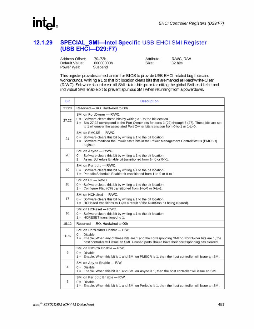
Intel® 82801DBM ICH4-M Datasheet 451
EHCI Controller Registers (D29:F7)
12.1.29 SPECIAL_SMI�Intel Specific USB EHCI SMI Register (USB EHCI�D29:F7)Address Offset: 70�73h Attribute: R/WC, R/WDefault Value: 00000000h Size: 32 bitsPower Well: Suspend
This register provides a mechanism for BIOS to provide USB EHCI related bug fixes and workarounds. Writing a 1 to that bit location clears bits that are marked as Read/Write-Clear (R/WC). Software should clear all SMI status bits prior to setting the global SMI enable bit and individual SMI enable bit to prevent spurious SMI when returning from a powerdown.
Bit Description
31:28 Reserved � RO. Hardwired to 00h
27:22
SMI on PortOwner � R/WC. 0 = Software clears these bits by writing a 1 to the bit location. 1 = Bits 27:22 correspond to the Port Owner bits for ports 1 (22) through 6 (27). These bits are set
to 1 whenever the associated Port Owner bits transition from 0-to-1 or 1-to-0.
21
SMI on PMCSR � R/WC. 0 = Software clears this bit by writing a 1 to the bit location. 1 = Software modified the Power State bits in the Power Management Control/Status (PMCSR)
register.
20SMI on Async � R/WC. 0 = Software clears this bit by writing a 1 to the bit location. 1 = Async Schedule Enable bit transitioned from 1->0 or 0->1.
19SMI on Periodic � R/WC. 0 = Software clears this bit by writing a 1 to the bit location. 1 = Periodic Schedule Enable bit transitioned from 1-to-0 or 0-to-1
18SMI on CF � R/WC. 0 = Software clears this bit by writing a 1 to the bit location. 1 = Configure Flag (CF) transitioned from 1-to-0 or 0-to-1.
17SMI on HCHalted � R/WC. 0 = Software clears this bit by writing a 1 to the bit location. 1 = HCHalted transitions to 1 (as a result of the Run/Stop bit being cleared).
16SMI on HCReset � R/WC. 0 = Software clears this bit by writing a 1 to the bit location. 1 = HCRESET transitioned to 1.
15:12 Reserved � RO. Hardwired to 00h
11:6
SMI on PortOwner Enable � R/W. 0 = Disable1 = Enable. When any of these bits are 1 and the corresponding SMI on PortOwner bits are 1, the
host controller will issue an SMI. Unused ports should have their corresponding bits cleared.
5SMI on PMSCR Enable � R/W. 0 = Disable1 = Enable. When this bit is 1 and SMI on PMSCR is 1, then the host controller will issue an SMI.
4SMI on Async Enable � R/W. 0 = Disable1 = Enable. When this bit is 1 and SMI on Async is 1, then the host controller will issue an SMI.
3SMI on Periodic Enable � R/W. 0 = Disable1 = Enable. When this bit is 1 and SMI on Periodic is 1, then the host controller will issue an SMI.

452 Intel® 82801DBM ICH4-M Datasheet
EHCI Controller Registers (D29:F7)
12.1.30 ACCESS_CNTL�Access Control Register (USB EHCI�D29:F7)Address Offset: 80h Attribute: R/WDefault Value: 00h Size: 8 bits
12.1.31 HS_Ref_V�USB HS Reference Voltage Register (USB EHCI�D29:F7)Offset Address: DC�DFh Attribute: R/WDefault Value: 00000000h Size: 32 bitLockable: No Power Well: Resume
2SMI on CF Enable � R/W. 0 = Disable1 = Enable. When this bit is 1 and SMI on CF is 1, then the host controller will issue an SMI.
1
SMI on HCHalted Enable � R/W. 0 = Disable1 = Enable. When this bit is a 1 and SMI on HCHalted is 1, then the host controller will issue an
SMI.
0
SMI on HCReset Enable � R/W. 0 = Disable1 = Enable. When this bit is a 1 and SMI on HCReset is 1, then host controller will issue an SMI�
R/W.
Bit Description
Bit Description
7:1 Reserved
0
WRT_RDONLY � R/W. 0 = Disable1 = Enables a select group of normally read-only registers in the EHC function to be written by
software. Registers that may only be written when this mode is entered are noted in the summary tables and detailed description as �Read/Write-Special�. The registers fall into two categories:- System-configured parameters, and- Status bits
Bit Description
31:22 Reserved� RO.
21:16 USB HS Ref Voltage � RW. BIOS should always program this register to the recommended value of 111111. All other values are reserved
15:0 Reserved� RO.

Intel® 82801DBM ICH4-M Datasheet 453
EHCI Controller Registers (D29:F7)
12.2 Memory-Mapped I/O RegistersThe USB 2.0 EHCI memory-mapped I/O space is composed of two sets of registers: Capability Registers and Operational Registers.
Note: When the USB EHCI function is in the D3 PCI power state, accesses to the USB EHCI memory range are ignored and result in a master abort. Similarly, if the Memory Space Enable (MSE) bit is not set in the Command register in configuration space, the memory range will not be decoded by the ICH4 Enhanced Host Controller (EHC). If the MSE bit is not set, the ICH4 must default to allowing any memory accesses for the range specified in the BAR to go to PCI. This is because the range may not be valid and, therefore, the cycle must be made available to any other targets that may be currently using that range.
12.2.1 Host Controller Capability RegistersThese registers specify the limits, restrictions and capabilities of the host controller implementation. Within the Host Controller Capability Registers, only the Structural Parameters register is writable. This register is implemented in the Suspend well and is only reset by the standard suspend-well hardware reset, not by HCRESET or the D3-to-D0 reset.
NOTE: �Read/Write-Special� means that the register is normally read-only, but may be written when the WRT_RDONLY bit is set. Because these registers are expected to be programmed by BIOS during initialization, their contents must not get modified by HCRESET or D3-to-D0 internal reset.
12.2.1.1 CAPLENGTH�Capability Registers Length RegisterOffset: 00h Attribute: RODefault Value: 20h Size: 8 bits
Table 12-2. Enhanced Host Controller Capability Registers
Offset Mnemonic Register Name Default Type
00h CAPLENGTH Capabilities Registers Length 20h RO
02�03h HCIVERSION Host Controller Interface Version Number 0100h RO
04�07h HCSPARAMS Host Controller Structural Parameters 00103206h R/W-Special
08�0Bh HCCPARAMS Host Controller Capability Parameters 00006871h RO
Bit Description
7:0Capability Register Length Value � RO. This register is used as an offset to add to the Memory Base Register to find the beginning of the Operational Register Space. This is fixed at 20h, indicating that the Operation Registers begin at offset 20h.

454 Intel® 82801DBM ICH4-M Datasheet
EHCI Controller Registers (D29:F7)
12.2.1.2 HCIVERSION�Host Controller Interface Version Number RegisterOffset: 02�03h Attribute: RODefault Value: 0100h Size: 16 bits
12.2.1.3 HCSPARAMS�Host Controller Structural Parameters RegisterOffset: 04�07h Attribute: R/W-SpecialDefault Value: 00103206h Size: 32 bits
Note: This register is reset by a suspend well reset and not a D3-to-D0 reset or HCRESET.
NOTE: This register is writable when the WRT_RDONLY bit is set.
Bit Description
15:0 This is a two-byte register containing a BCD encoding of the version number of interface that this host controller interface conforms.
Bit Description
31:24 Reserved � RO. Default=0h.
23:20 Debug Port Number (DP_N) � R/W-Special. Hardwired to 1h; indicates that the Debug Port is on the lowest numbered port on the ICH4.
19:17 Reserved
16 Reserved. Should be written to 0.
15:12
Number of Companion Controllers (N_CC) � R/W-Special. This field indicates the number of companion controllers associated with this USB ECHI host controller.A 0h in this field indicates there are no companion host controllers. Port-ownership hand-off is not supported. Only high-speed devices are supported on the host controller root ports.A value larger than 1 in this field indicates there are companion USB UHCI host controller(s). Port-ownership hand-offs are supported. High, Full- and Low-speed devices are supported on the host controller root ports.The ICH4 allows the default value of 3h to be over-written by BIOS. Since the ICH4 cannot support more than 3 companion host controllers, bits 15:14 are implemented as read-only 00b. When removing classic controllers, they should be disabled in the following order: Function 2, Function 1, and Function 0, which correspond to ports 5:4, 3:2, and 1:0, respectively.
11:8Number of Ports per Companion Controller (N_PCC) � RO. Hardwired to 0010. This field indicates the number of ports supported per companion host controller. It is used to indicate the port routing configuration to system software.
7:4 Reserved. These bits are reserved and default to 0h.
3:0
N_PORTS � R/W-Special. This field specifies the number of physical downstream ports implemented on this host controller. The value of this field determines how many port registers are addressable in the Operational Register Space. Valid values are in the range of 1h to Fh. The default is 0110 (6h). However, software may write a value less than 6 for some platform configurations. A 0h in this field is undefined. Bit 3 is always hardwired to 0.

Intel® 82801DBM ICH4-M Datasheet 455
EHCI Controller Registers (D29:F7)
12.2.1.4 HCCPARAMS�Host Controller Capability Parameters RegisterOffset: 08�0Bh Attribute: RODefault Value: 00006871h Size: 32 bits
Bit Description
31:16 Reserved
15:8 EHCI Extended Capabilities Pointer (EECP) � RO. Hardwired to 68h, indicating that the EHCI capabilities list exists and begins at offset 68h in the PCI configuration space.
7:4
Isochronous Scheduling Threshold � RO. Hardwired to 7h (0111). This field indicates, relative to the current position of the executing host controller, where software can reliably update the isochronous schedule. When bit 7 is 0, the value of the least significant 3 bits indicates the number of micro-frames a host controller hold a set of isochronous data structures (one or more) before flushing the state. When bit 7 is a 1, host software assumes the host controller may cache an isochronous data structure for an entire frame. Refer to the EHCI specification for details on how software uses this information for scheduling isochronous transfers.
3 Reserved. Should be set to 0.
2 Asynchronous Schedule Park Capability � RO. Hardwired to 0, indicating that the Host Controller does not support this optional feature
1
Programmable Frame List Flag � RO.0 = System software must use a frame list length of 1024 elements with this host controller. The
USBCMD register Frame List Size field is a read-only register and must be set to zero.1 = System software can specify and use a smaller frame list and configure the host controller via
the USBCMD register Frame List Size field. The frame list must always be aligned on a 4K page boundary. This requirement ensures that the frame list is always physically contiguous.
0
64-bit Addressing Capability� RO. Hardwired to 1. This field documents the addressing range capability of this implementation. The value of this field determines whether software should use the 32-bit or 64-bit data structures. Values for this field have the following interpretation:0 = Data structures using 32-bit address memory pointers1 = Data structures using 64-bit address memory pointers NOTE: The ICH4 only implements 44 bits of addressing. Bits 63:44 will always be 0.

456 Intel® 82801DBM ICH4-M Datasheet
EHCI Controller Registers (D29:F7)
12.2.2 Host Controller Operational RegistersThis section defines the enhanced host controller operational registers. These registers are located after the capabilities registers. The operational register base must be DWord-aligned and is calculated by adding the value in the first capabilities register (CAPLENGTH) to the base address of the enhanced host controller register address space. All registers are 32 bits in length.
Note: Software must read and write these registers using only DWord accesses.These registers are divided into two sets. The first set at offset 00:3Fh are implemented in the core power well. Unless otherwise noted, the core-well registers are reset by the assertion of any of the following:
� core well hardware reset� HCRESET� D3-to-D0 reset
The second set at offset 40h to the end of the implemented register space are implemented in the Suspend power well. Unless otherwise noted, the suspend-well registers are reset by the assertion of either of the following:
� suspend well hardware reset� HCRESET
Table 12-3. Enhanced Host Controller Operational RegistersOffset
(CAPLENGTH+)
Mnemonic Register Name Default Special Notes Type
00�03h EHCI_CMD USB EHCI Command 00080000h R/W, RO04�07h EHCI_STS USB EHCI Status 00001000h R/WC, RO08�0Bh EHCI_INTR USB EHCI Interrupt Enable 00000000h R/W0C�0Fh FRINDEX USB EHCI Frame Index 00000000h R/W
10�13h CTRLDSSEGMENT Control Data Structure Segment 00000000h R/W
14�17h PERIODICLISTBASE Period Frame List Base Address 00000000h R/W
18�1Bh ASYNCLISTADDR Next Asynchronous List Address 00000000h R/W
1C�3Fh Reserved 0h RO40�43h CONFIGFLAG Configure Flag Register 00000000h Suspend R/W
44�47h PORTSC0 Port 0 Status and Control 00003000h Suspend R/WC, R/W, RO
48�4Bh PORTSC1 Port 1 Status and Control 00003000h Suspend R/WC, R/W, RO
4C�4Fh PORTSC2 Port 2 Status and Control 00003000h Suspend R/WC, R/W, RO
50�53h PORTSC3 Port 3 Status and Control 00003000h Suspend R/WC, R/W, RO
54�57h PORTSC4 Port 4 Status and Control 00003000h Suspend R/WC, R/W, RO
58�5Bh PORTSC5 Port 5 Status and Control 00003000h Suspend R/WC, R/W, RO
5C�5Fh Reserved Undefined RO60�73h Debug Port Registers Undefined RO
74�3FFh Reserved Undefined RO

Intel® 82801DBM ICH4-M Datasheet 457
EHCI Controller Registers (D29:F7)
12.2.2.1 EHCI_CMD�USB EHCI Command RegisterOffset: CAPLENGTH + 00�03h Attribute: R/W, RODefault Value: 00080000h Size: 32 bits
Bit Description
31:24 Reserved. Should be set to 0s.
23:16
Interrupt Threshold Control R/W. This field is used by system software to select the maximum rate at which the host controller will issue interrupts. The only valid values are defined below. If software writes an invalid value to this register, the results are undefined.00h = Reserved01h = 1 micro-frame02h = 2 micro-frames04h = 4 micro-frames08h = 8 micro-frames (default, equates to 1 ms)10h = 16 micro-frames (2 ms)20h = 32 micro-frames (4 ms)40h = 64 micro-frames (8 ms)
15:8 Reserved. Should be set to 0s.
11:8 Unimplemented Asynchronous Park Mode Bits � RO. Hardwired to 000b; the host controller does not support this optional feature.
7 Light Host Controller Reset � RO. Hardwired to 0; the ICH4 does not implement this optional reset.
6
Interrupt on Async Advance Doorbell � R/W. This bit is used as a doorbell by software to tell the host controller to issue an interrupt the next time it advances asynchronous schedule. 0 = The host controller sets this bit to a 0 after it has set the Interrupt on Async Advance status bit in
the EHCI_STS register to a 1. 1 = Software must write a 1 to this bit to ring the doorbell. When the host controller has evicted all
appropriate cached schedule state, it sets the Interrupt on Async Advance status bit in the EHCI_STS register. If the Interrupt on Async Advance Enable bit in the USBINTR register is a 1 then the host controller will assert an interrupt at the next interrupt threshold. See the Enhanced Host Controller Interface (EHCI) Specification for Universal Serial Bus for operational details.
Software should not write a 1 to this bit when the asynchronous schedule is inactive. Doing this will yield undefined results.
5
Asynchronous Schedule Enable R/W. This bit controls whether the host controller skips processing the Asynchronous Schedule. 0 = Do not process the Asynchronous Schedule (Default) 1 = Use the ASYNCLISTADDR register to access the Asynchronous Schedule.
4
Periodic Schedule Enable R/W. This bit controls whether the host controller skips processing the Periodic Schedule. 0 = Do not process the Periodic Schedule (Default)1 = Use the PERIODICLISTBASE register to access the Periodic Schedule.
3:2 Frame List Size RO. Hardwired to 00; ICH4 only supports the 1024-element frame list size.

458 Intel® 82801DBM ICH4-M Datasheet
EHCI Controller Registers (D29:F7)
NOTE: The Command Register indicates the command to be executed by the serial bus host controller. Writing to the register causes a command to be executed.
1
Host Controller Reset (HCRESET) R/W. This control bit used by software to reset the host controller. The effects of this on Root Hub registers are similar to a Chip Hardware Reset (i.e., RSMRST# assertion and PWROK deassertion on the ICH4). 0 = This bit is set to 0 by the Host Controller when the reset process is complete. Software cannot
terminate the reset process early by writing a 0 to this bit. 1 = When software writes a 1 to this bit, the Host Controller resets its internal pipelines, timers,
counters, state machines, etc. to their initial value. Any transaction currently in progress on USB is immediately terminated. A USB reset is not driven on downstream ports.
All operational registers, including port registers and port state machines are set to their initial values. Port ownership reverts to the companion host controller(s), with the side effects described in the EHCI spec. Software must re-initialize the host controller in order to return the host controller to an operational state.
Software should not set this bit to a 1 when the HCHalted bit in the EHCI_STS register is a 0. Attempting to reset an actively running host controller will result in undefined behavior. This reset me be used to leave EHCI port test modes.
NOTE: PCI Configuration registers and Host Controller Capability Registers are not effected by this reset.
0
Run/Stop (RS) R/W. 0 = Stop (Default)1 = Run. When set to a 1, the Host Controller proceeds with execution of the schedule. The Host
Controller continues execution as long as this bit is set. When this bit is set to 0, the Host Controller completes the current transaction on the USB and then halts. The HC Halted bit in the status register indicates when the Host Controller has finished the transaction and has entered the stopped state.
NOTE: Software should not write a 1 to this field unless the host controller is in the Halted state (i.e., HCHalted in the EHCI_STS register is a 1). The Halted bit is cleared immediately when the Run bit is set.
The following table explains how the different combinations of Run and Halted should be interpreted:Run/StopHaltedInterpretation0 0 Valid- in the process of halting0 1 Valid- halted1 0 Valid- running1 1 Invalid- the HCHalted bit clears immediately.Memory read cycles initiated by the EHC that receive any status other than Successful will result in this bit being cleared.
Bit Description

Intel® 82801DBM ICH4-M Datasheet 459
EHCI Controller Registers (D29:F7)
12.2.2.2 EHCI_STS�USB EHCI Status RegisterOffset: CAPLENGTH + 04�07h Attribute: R/WC, RODefault Value: 00001000h Size: 32 bits
This register indicates pending interrupts and various states of the Host Controller. The status resulting from a transaction on the serial bus is not indicated in this register. Software sets a bit to 0 in this register by writing a 1 to it. See the Interrupts description in Chapter 4 of the Enhanced Host Controller Interface (EHCI) Specification for Universal Serial Bus for additional information concerning USB EHCI interrupt conditions.
Bit Description
31:16 Reserved. Should be set to 0s.
15
Asynchronous Schedule Status RO. This bit reports the current real status of the Asynchronous Schedule. The Host Controller is not required to immediately disable or enable the Asynchronous Schedule when software transitions the Asynchronous Schedule Enable bit in the USBCMD register. When this bit and the Asynchronous Schedule Enable bit are the same value, the Asynchronous Schedule is either enabled (1) or disabled (0).0 = Disable. (Default)1 = Enable. The status of the Asynchronous Schedule is enabled.
14
Periodic Schedule Status RO. This bit reports the current real status of the Periodic Schedule. The Host Controller is not required to immediately disable or enable the Periodic Schedule when software transitions the Periodic Schedule Enable bit in the USBCMD register. When this bit and the Periodic Schedule Enable bit are the same value, the Periodic Schedule is either enabled (1) or disabled (0). 0 = Disable. (Default). 1 = Enable. The status of the Periodic Schedule is enabled.
13Reclamation RO. (Defaults to 1). This bit is used to detect an empty asynchronous schedule. The operational model and valid transitions for this bit are described in Section 4 of the EHCI Specification.
12
HCHalted RO. 0 = This bit is a 0 when the Run/Stop bit is a 1. 1 = The Host Controller sets this bit to 1 after it has stopped executing as a result of the Run/Stop
bit being set to 0, either by software or by the Host Controller hardware (e.g., internal error). (Default)
11:6 Reserved
5
Interrupt on Async Advance � R/WC. 0=Default. 0 = Interrupt not occurred (source not asserted).1 = Interrupt occurred (source asserted). System software can force the host controller to issue an
interrupt the next time the host controller advances the asynchronous schedule by writing a 1 to the Interrupt on Async Advance Doorbell bit in the USBCMD register. This bit indicates the assertion of that interrupt source.
4
Host System Error � RO. 0 = No host system error during access of the Host Controller module. 1 = Host system error. The Host Controller sets this bit to 1 when a serious error occurs during a
host system access involving the Host Controller module. A hardware interrupt is generated to the system. Memory read cycles initiated by the EHC that receive any status other than Successful will result in this bit being set.
When this error occurs, the Host Controller clears the Run/Stop bit in the Command register to prevent further execution of the scheduled TDs. A hardware interrupt is generated to the system (if enabled in the Interrupt Enable Register).

460 Intel® 82801DBM ICH4-M Datasheet
EHCI Controller Registers (D29:F7)
3
Frame List Rollover � R/WC.0 = No rollover.1 = Frame List Rollover. The Host Controller sets this bit to a 1 when the Frame List Index (see
Section) rolls over from its maximum value to zero. Since the ICH4 only supports the 1024-entry Frame List Size, the Frame List Index rolls over every time FRNUM[13] toggles.
2
Port Change Detect � R/WC.0 = Not Detected. 1 = Port Change Detected. The Host Controller sets this bit to a 1 when any port for which the Port
Owner bit is set to 0 has a change bit transition from 0 to 1 or a Force Port Resume bit transition from 0 to 1 as a result of a J-K transition detected on a suspended port.
1
USB Error Interrupt (USBERRINT) � R/WC. 0 = No Error. 1 = Error Condition. The Host Controller sets this bit to 1 when completion of a USB transaction
results in an error condition (e.g., error counter underflow). If the TD on which the error interrupt occurred also had its IOC bit set, both this bit and Bit 0 are set. See the EHCI specification for a list of the USB errors that will result in this interrupt being asserted.
0
USB Interrupt (USBINT) � R/WC. 0 = Software clears this bit by writing a 1 to the bit location. 1 = The Host Controller sets this bit to 1 when one of the following occurs:
�The cause of an interrupt is a completion of a USB transaction whose Transfer Descriptor had its IOC bit set.
�The Host Controller also sets this bit to 1 when a short packet is detected (actual number of bytes received was less than the expected number of bytes).
Bit Description

Intel® 82801DBM ICH4-M Datasheet 461
EHCI Controller Registers (D29:F7)
12.2.2.3 EHCI_INTR�USB EHCI Interrupt Enable RegisterOffset: CAPLENGTH + 08�0Bh Attribute: R/WDefault Value: 00000000h Size: 32 bits
This register enables and disables reporting of the corresponding interrupt to the software. When a bit is set and the corresponding interrupt is active, an interrupt is generated to the host. Interrupt sources that are disabled in this register still appear in the Status Register to allow the software to poll for events. Each interrupt enable bit description indicates whether it is dependent on the interrupt threshold mechanism, or not (see Chapter 4 of the Enhanced Host Controller Interface (EHCI) Specification for Universal Serial Bus).
Bit Description
31:6 Reserved. Should be 0s.
5
Interrupt on Async Advance Enable � R/W. When this bit is a 1, and the Interrupt on Async Advance bit in the EHCI_STS register is a 1, the host controller will issue an interrupt at the next interrupt threshold. The interrupt is acknowledged by software clearing the Interrupt on Async Advance bit in the EHCI_STS register.0 = Disable1 = Enable
4
Host System Error Enable � R/W. When this bit is a 1, and the Host System Error Status bit in the EHCI_STS register is a 1, the host controller will issue an interrupt. The interrupt is acknowledged by software clearing the Host System Error bit in the EHCI_STS register.0 = Disable1 = Enable
3
Frame List Rollover Enable � R/W. When this bit is a 1, and the Frame List Rollover bit in the EHCI_STS register is a 1, the host controller will issue an interrupt. The interrupt is acknowledged by software clearing the Frame List Rollover bit in the EHCI_STS register.0 = Disable1 = Enable
2
Port Change Interrupt Enable � R/W. When this bit is a 1, and the Port Change Detect bit in the EHCI_STS register is a 1, the host controller will issue an interrupt. The interrupt is acknowledged by software clearing the Port Change Detect bit in the EHCI_STS register.0 = Disable1 = Enable
1
USB Error Interrupt Enable � R/W. When this bit is a 1, and the USBERRINT bit in the EHCI_STS register is a 1, the host controller will issue an interrupt at the next interrupt threshold. The interrupt is acknowledged by software by clearing the USBERRINT bit in the EHCI_STS register. 0 = Disable1 = Enable
0
USB Interrupt Enable � R/W. When this bit is a 1, and the USBINT bit in the EHCI_STS register is a 1, the host controller will issue an interrupt at the next interrupt threshold. The interrupt is acknowledged by software by clearing the USBINT bit in the EHCI_STS register.0 = Disable1 = Enable

462 Intel® 82801DBM ICH4-M Datasheet
EHCI Controller Registers (D29:F7)
12.2.2.4 FRINDEX�Frame Index RegisterOffset: CAPLENGTH + 0C�0Fh Attribute: R/WDefault Value: 00000000h Size: 32 bits
The SOF frame number value for the bus SOF token is derived or alternatively managed from this register. Refer to Section 4 of the EHCI specification for a detailed explanation of the SOF value management requirements on the host controller. The value of FRINDEX must be within 125 µs (1 micro-frame) ahead of the SOF token value. The SOF value may be implemented as an 11-bit shadow register. For this discussion, this shadow register is 11 bits and is named SOFV. SOFV updates every 8 micro-frames. (1 millisecond). An example implementation to achieve this behavior is to increment SOFV each time the FRINDEX[2:0] increments from 0 to 1.
Software must use the value of FRINDEX to derive the current micro-frame number, both for high-speed isochronous scheduling purposes and to provide the get micro-frame number function required to client drivers. Therefore, the value of FRINDEX and the value of SOFV must be kept consistent if chip is reset or software writes to FRINDEX. Writes to FRINDEX must also write-through FRINDEX[13:3] to SOFV[10:0]. In order to keep the update as simple as possible, software should never write a FRINDEX value where the three least significant bits are 111b or 000b.
Note: This register is used by the host controller to index into the periodic frame list. The register updates every 125 microseconds (once each micro-frame). Bits [12:3] are used to select a particular entry in the Periodic Frame List during periodic schedule execution. The number of bits used for the index is fixed at 10 for the ICH4 since it only supports 1024-entry frame lists. This register must be written as a DWord. Word and byte writes produce undefined results. This register cannot be written unless the Host Controller is in the Halted state as indicated by the HCHalted bit (USB EHCI STS register). A write to this register while the Run/Stop bit is set to a 1 (USB EHCI CMD register) produces undefined results. Writes to this register also effect the SOF value. For details, see Chapter 4 of the Enhanced Host Controller Interface (EHCI) Specification for Universal Serial Bus.
Bit Description
31:14 Reserved
13:0
Frame List Current Index/Frame Number � R/W. The value in this register increments at the end of each time frame (e.g., micro-frame). Bits [12:3] are used for the Frame List current index. This means that each location of the frame list is accessed 8 times (frames or micro-frames) before moving to the next index.

Intel® 82801DBM ICH4-M Datasheet 463
EHCI Controller Registers (D29:F7)
12.2.2.5 CTRLDSSEGMENT�Control Data Structure Segment RegisterOffset: CAPLENGTH + 10�13h Attribute: R/WDefault Value: 00000000h Size: 32 bits
This 32-bit register corresponds to the most significant address bits [63:32] for all EHCI data structures. Since the ICH4 hardwires the 64-bit Addressing Capability field in HCCPARAMS to 1s, then this register is used with the link pointers to construct 64-bit addresses to EHCI control data structures. This register is concatenated with the link pointer from either the PERIODICLISTBASE, ASYNCLISTADDR, or any control data structure link field to construct a 64-bit address. This register allows the host software to locate all control data structures within the same 4 GB memory segment.
12.2.2.6 PERIODICLISTBASE�Periodic Frame List Base Address RegisterOffset: CAPLENGTH + 14�17h Attribute: R/WDefault Value: 00000000h Size: 32 bits
This 32-bit register contains the beginning address of the Periodic Frame List in the system memory. Since the ICH4 host controller operates in 64-bit mode (as indicated by the one in the 64-bit Addressing Capability field in the HCCSPARAMS register), then the most significant 32 bits of every control data structure address comes from the CTRLDSSEGMENT register. HCD loads this register prior to starting the schedule execution by the Host Controller. The memory structure referenced by this physical memory pointer is assumed to be 4-KB aligned. The contents of this register are combined with the Frame Index Register (FRINDEX) to enable the Host Controller to step through the Periodic Frame List in sequence.
Bit Description
31:12 Upper Address [63:44] � R/W. These bits are hardwired, read-only to 0 in the ICH4. The ICH4 EHC is only capable of generating addresses up to 16 terabytes (44 bits of address).
11:0 Upper Address [43:32] � R/W. This 12-bit field corresponds to address bits 43:32 when forming a control data structure address.
Bit Description
31:12 Base Address (Low) � R/W. These bits correspond to memory address signals [31:12], respectively.
11:0 Reserved. Must be written as 0s. During runtime, the value of these bits are undefined.
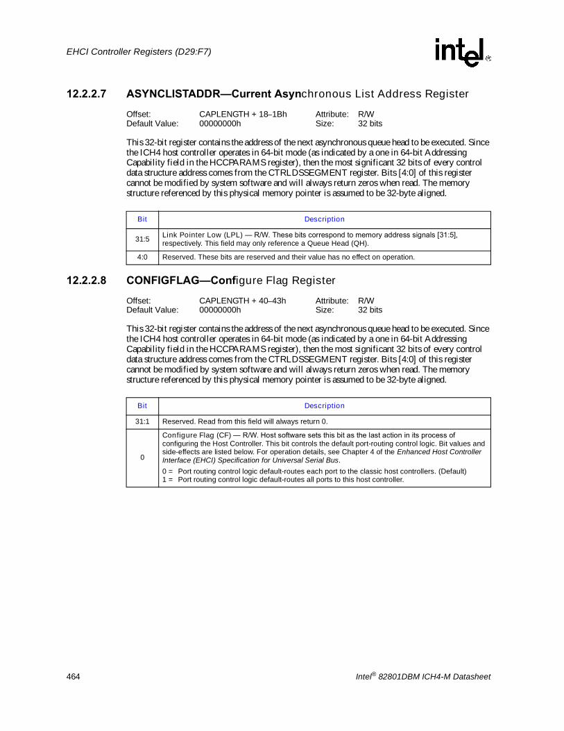
464 Intel® 82801DBM ICH4-M Datasheet
EHCI Controller Registers (D29:F7)
12.2.2.7 ASYNCLISTADDR�Current Asynchronous List Address RegisterOffset: CAPLENGTH + 18�1Bh Attribute: R/WDefault Value: 00000000h Size: 32 bits
This 32-bit register contains the address of the next asynchronous queue head to be executed. Since the ICH4 host controller operates in 64-bit mode (as indicated by a one in 64-bit Addressing Capability field in the HCCPARAMS register), then the most significant 32 bits of every control data structure address comes from the CTRLDSSEGMENT register. Bits [4:0] of this register cannot be modified by system software and will always return zeros when read. The memory structure referenced by this physical memory pointer is assumed to be 32-byte aligned.
12.2.2.8 CONFIGFLAG�Configure Flag RegisterOffset: CAPLENGTH + 40�43h Attribute: R/WDefault Value: 00000000h Size: 32 bits
This 32-bit register contains the address of the next asynchronous queue head to be executed. Since the ICH4 host controller operates in 64-bit mode (as indicated by a one in 64-bit Addressing Capability field in the HCCPARAMS register), then the most significant 32 bits of every control data structure address comes from the CTRLDSSEGMENT register. Bits [4:0] of this register cannot be modified by system software and will always return zeros when read. The memory structure referenced by this physical memory pointer is assumed to be 32-byte aligned.
Bit Description
31:5 Link Pointer Low (LPL) � R/W. These bits correspond to memory address signals [31:5], respectively. This field may only reference a Queue Head (QH).
4:0 Reserved. These bits are reserved and their value has no effect on operation.
Bit Description
31:1 Reserved. Read from this field will always return 0.
0
Configure Flag (CF) � R/W. Host software sets this bit as the last action in its process of configuring the Host Controller. This bit controls the default port-routing control logic. Bit values and side-effects are listed below. For operation details, see Chapter 4 of the Enhanced Host Controller Interface (EHCI) Specification for Universal Serial Bus. 0 = Port routing control logic default-routes each port to the classic host controllers. (Default)1 = Port routing control logic default-routes all ports to this host controller.

Intel® 82801DBM ICH4-M Datasheet 465
EHCI Controller Registers (D29:F7)
12.2.2.9 PORTSC�Port N Status and Control RegisterOffset: Port 0 CAPLENGTH + 44�47h
Port 1 CAPLENGTH + 48�4BhPort 2 CAPLENGTH + 4C�4FhPort 3 CAPLENGTH + 50�53hPort 4 CAPLENGTH + 54�57hPort 5 CAPLENGTH + 58�5Bh
Attribute: R/W, R/WC, RODefault Value: 00003000h Size: 32 bits
A host controller must implement one or more port registers. Software uses the N_Port information from the Structural Parameters Register to determine how many ports need to be serviced. All ports have the structure defined below. Software must not write to unreported Port Status and Control Registers.
This register is in the suspend power well. It is only reset by hardware when the suspend power is initially applied or in response to a host controller reset. The initial conditions of a port are:
� No device connected,� Port disabled.
When a device is attached, the port state transitions to the attached state and system software will process this as with any status change notification. Refer to Chapter 4 of the Enhanced Host Controller Interface (EHCI) Specification for Universal Serial Bus for operational requirements for how change events interact with port suspend mode.
Bit Description
31:23 Reserved. These bits are reserved for future use and will return a value of 0s when read.
22
Wake on Over-current Enable (WKOC_E) � RW. 0 = Disable. (Default) 1 = Enable. Writing this bit to a 1 enables the setting of the PME Status bit in the Power
Management Control/Status Register (offset 54, bit 15) when the Over-current Active bit (bit 4 of this register) is set to 1.
21
Wake on Disconnect Enable (WKDSCNNT_E) � RW. Default = 0b. 0 = Disable. (Default) 1 = Enable. Writing this bit to a 1 enables the setting of the PME Status bit in the Power
Management Control/Status Register (offset 54, bit 15) when the Current Connect Status changes from connected to disconnected (i.e., bit 0 of this register changes from 1 to 0).
20
Wake on Connect Enable (WKCNNT_E) � RW.0 = Disable. (Default) 1 = Enable. Writing this bit to a 1 enables the setting of the PME Status bit in the Power
Management Control/Status Register (offset 54, bit 15) when the Current Connect Status changes from disconnected to connected (i.e., bit 0 of this register changes from 0 to 1).
19:16
Port Test Control � RW. When this field is 0, the port is NOT operating in a test mode. A non-zero value indicates that it is operating in test mode and the specific test mode is indicated by the specific value. Refer to Universal Serial Bus (USB) Specification, Revision 2.0, Chapter 7 for details on each test mode.BitsTest Mode0000Test mode Not enabled (Default)0001Test J_STATE0010Test K_STATE0011Test SE0_NAK0100Test Packet0101Test FORCE_ENABLE0110�1111Reserved

466 Intel® 82801DBM ICH4-M Datasheet
EHCI Controller Registers (D29:F7)
15:14 Reserved � RW. Should be written to =00b.
13
Port Owner � RW. Default = 1b. This bit unconditionally goes to a 0 when the Configured Flag bit in the CONFIGFLAG register makes a 0-to-1 transition. System software uses this field to release ownership of the port to a selected host controller (in the event that the attached device is not a high-speed device). Software writes a 1 to this bit when the attached device is not a high-speed device. A 1 in this bit means that a companion host controller owns and controls the port. For operational details, see Chapter 4 of the Enhanced Host Controller Interface (EHCI) Specification for Universal Serial Bus.
12 Port Power (PP) RO. Hardwired to 1. This indicates that the port does have power.
11:10
Line Status� RO.These bits reflect the current logical levels of the D+ (bit 11) and D- (bit 10) signal lines. These bits are used for detection of low-speed USB devices prior to the port reset and enable sequence. This field is valid only when the port enable bit is 0 and the current connect status bit is set to a 1.00 = SE010 = J-state01 = K-state11 = Undefined
9 Reserved. This bit will return a 0 when read.
8
Port Reset � RW. When software writes a 1 to this bit (from a 0), the bus reset sequence as defined in the Universal Serial Bus (USB) Specification, Revision 2.0 is started. Software writes a 0 to this bit to terminate the bus reset sequence. Software must keep this bit at a 1 long enough to ensure the reset sequence completes, as specified in the Universal Serial Bus (USB) Specification, Revision 2.0. 0 = Port is not in Reset. (Default)1 = Port is in Reset.
NOTE: When software writes this bit to a 1, it must also write a 0 to the Port Enable bit. When software writes a 0 to this bit, there may be a delay before the bit status changes to a 0. The bit status will not read as a 0 until after the reset has completed. If the port is in high-speed mode after reset is complete, the host controller will automatically enable this port (e.g., set the Port Enable bit to a 1). A host controller must terminate the reset and stabilize the state of the port within 2 milliseconds of software transitioning this bit from 1 to 0.
For example: if the port detects that the attached device is high-speed during reset, then the host controller must have the port in the enabled state within 2 ms of software writing this bit to a 0. The HCHalted bit in the EHCI_STS register should be a 0 before software attempts to use this bit. The host controller may hold Port Reset asserted to a 1 when the HCHalted bit is a 1. This field is 0 if Port Power is 0.
Warning:System software should not attempt to reset a port if the HCHalted bit in the EHCI_STS register is a 1. Doing so will result in undefined behavior.
7
Suspend � RW.0 = Port not in suspend state. (Default). 1 = Port in suspend state. Port Enabled Bit and Suspend bit of this register define the port states as follows:Bits [Port Enabled, Suspend]Port State
0X Disable10 Enable11 Suspend
� When in suspend state, downstream propagation of data is blocked on this port, except for port reset. Note that the bit status does not change until the port is suspended and that there may be a delay in suspending a port depending on the activity on the port.
� The host controller will unconditionally set this bit to a 0 when software sets the Force Port Resume bit to a 0 (from a 1). A write of 0 to this bit is ignored by the host controller.
� If host software sets this bit to a 1 when the port is not enabled (i.e., Port enabled bit is a 0) the results are undefined.
Bit Description

Intel® 82801DBM ICH4-M Datasheet 467
EHCI Controller Registers (D29:F7)
6
Force Port Resume � RW. Software sets this bit to a 1 to drive resume signaling. The Host Controller sets this bit to a 1 if a J-to-K transition is detected while the port is in the Suspend state. When this bit transitions to a 1 because a J-to-K transition is detected, the Port Change Detect bit in the EHCI_STS register is also set to a 1. If software sets this bit to a 1, the host controller must not set the Port Change Detect bit.0 = No resume (K-state) detected/driven on port. (Default). 1 = Resume detected/driven on port. NOTE: When the EHCI controller owns the port, the resume sequence follows the defined
sequence documented in the Universal Serial Bus (USB) Specification, Revision 2.0. The resume signaling (Full-speed 'K') is driven on the port as long as this bit remains a 1. Software must appropriately time the Resume and set this bit to a 0 when the appropriate amount of time has elapsed. Writing a 0 (from 1) causes the port to return to high-speed mode (forcing the bus below the port into a high-speed idle). This bit will remain 1 until the port has switched to the high-speed idle.
5
Overcurrent Change� R/WC. Default = 0. The functionality of this bit is not dependent upon the port owner.0 = Software clears this bit by writing a 1 to this bit position. 1 = There is a change to Over-current Active.
4
Overcurrent Active � RO. The ICH4 automatically disables the port when the over-current active bit is 1. 0 = This port does not have an over-current condition. This bit will automatically transition from a
1-to-0 when the over current condition is removed. (Default)1 = This port currently has an over-current condition.
3
Port Enable/Disable Change � R/WC. For the root hub, this bit gets set to a 1 only when a port is disabled due to the appropriate conditions existing at the EOF2 point (See Chapter 11 of the Universal Serial Bus (USB) Specification, Revision 2.0 for the definition of a port error). This bit is not set due to the Disabled-to-Enabled transition, nor due to a disconnect. 0 = No change in status. (Default). Software clears this bit by writing a 1 to it.1 = Port enabled/disabled status has changed.
2
Port Enabled/Disabled � R/W. Ports can only be enabled by the host controller as a part of the reset and enable. Software cannot enable a port by writing a 1 to this field. Ports can be disabled by either a fault condition (disconnect event or other fault condition) or by host software. Note that the bit status does not change until the port state actually changes. There may be a delay in disabling or enabling a port due to other host controller and bus events.0 = Disable. (Default)1 = Enable.
1
Connect Status Change � R/WC. A 1 indicates a change has occurred in the port�s Current Connect Status. The host controller sets this bit for all changes to the port device connect status, even if system software has not cleared an existing connect status change. For example, the insertion status changes twice before system software has cleared the changed condition, hub hardware will be �setting� an already-set bit (i.e., the bit will remain set). 0 = No change. (Default). Software sets this bit to 0 by writing a 1 to it.1 = Change in Current Connect Status.
0
Current Connect Status � RO. This value reflects the current state of the port, and may not correspond directly to the event that caused the Connect Status Change bit (Bit 1) to be set.0 = No device is present. (Default)1 = Device is present on port.
Bit Description

468 Intel® 82801DBM ICH4-M Datasheet
EHCI Controller Registers (D29:F7)
12.2.3 USB 2.0-Based Debug Port RegisterThe Debug port�s registers are located in the same memory area, defined by the Base Address Register (BAR), as the standard EHCI registers. The base offset for the debug port registers (80h) is declared in the Debug Port Base Offset Capability Register at Configuration offset 5Ah. The specific EHCI port that supports this debug capability is indicated by a 4-bit field (bits 20�23) in the HCSPARAMS register of the EHCI controller.
The map of the Debug Port registers is shown in Table 12-4. Each register is defined individually below.
NOTES:1. All of these registers are implemented in the core well and reset by PCIRST#, EHC HCRESET, and a EHC
D3-to-D0 transition.2. The hardware associated with this register provides no checks to ensure that software programs the interface
correctly. How the hardware behaves when programmed illegally is undefined.
12.2.3.1 Control/Status RegisterOffset: 00h Attribute: R/W, RODefault Value: 00000000h Size: 32 bits
Note: Software should do Read-Modify-Write operations to this register to preserve the contents of bits not being modified. This include Reserved bits.
Note: To preserve the usage of RESERVED bits in the future, software should always write the same value read from the bit until it is defined. Reserved bits will always return 0 when read.
Table 12-4. Debug Port Register Address Map
Offset Register Name Type
00h Control/Status R/W, RO
04h USB PIDs R/W, RO
08h Data Buffer (Bytes 3:0) R/W
0Ch Data Buffer (Bytes 7:4) R/W
10h Config Register R/W
Bit Description
31 Reserved
30
OWNER_CNT � R/W. 0 = Default.1 = Ownership of the debug port is forced to the EHCI controller (i.e., immediately taken away
from the companion Classic USB Host Controller). If the port was already owned by the EHCI controller, then setting this bit has no effect. This bit overrides all of the ownership-related bits in the standard EHCI registers.
29 Reserved

Intel® 82801DBM ICH4-M Datasheet 469
EHCI Controller Registers (D29:F7)
28
ENABLED_CNT � R/W. 0 = Software can clear this bit by writing a 0 to it. Hardware clears the bit for the same conditions
where the Port Enable/Disable Change bit (in the PORTSC register) is set. (Default)1 = Enable debug port for operation. Software can directly set this bit if the port is already enabled
in the associated Port Status and Control register (this is enforced by the hardware).
27:17 Reserved
16DONE_STS � R/WC. 0 = Not Done (Default). Software clears this bit by writing a 1 to it. 1 = This bit is set by hardware to indicate that the request is complete.
15:12 LINK_ID_STS � RO. Hardwired to 0000. This field identifies the link interface. It is hardwired to 0h to indicate that it is a USB Debug Port.
11 Reserved. This bit will return 0 when read. Writes will have no effect.
10
IN_USE_CNT � R/W. (This bit has no affect on hardware.)0 = Not in Use. Cleared by software to indicate that the port is free and may be used by other
software. (Default)1 = In Use. Set by software to indicate that the port is in use.
9:7
EXCEPTION_STS � RO. Default=000b This field indicates the exception when the ERROR_GOOD#_STS bit is set. This field should be ignored if the ERROR_GOOD#_STS bit is 0.000 =No Error. Note: this should not be seen, since this field should only be checked if there is an
error.001 =Transaction error: indicates the USB EHCI transaction had an error (CRC, bad PID, timeout,
etc.)010 =HW error. Request was attempted (or in progress) when port was suspended or reset.All Others = Reserved
6
ERROR_GOOD#_STS � RO. 0 = Hardware clears this bit upon the proper completion of a read or write. (Default)1 = Error Occurred. The hardware sets this bit to indicate that an error has occurred. Details on
the nature of the error are provided in the Exception field.
5
GO_CNT � WO. 0 = Hardware clears this bit when hardware sets the DONE_STS bit. (Default)1 = Causes hardware to perform a read or write request. Writing a 1 to this bit when it is already
set may result in undefined behavior.
4WRITE_READ#_CNT � R/W. 0 = Read. Software clears this bit to indicate that the current request is a read. (Default)1 = Write. Software sets this bit to indicate that the current request is a write.
3:0
DATA_LEN_CNT � R/W. This field is used to indicate the size of the data to be transferred. (default = 0h).For write operations, this field is set by software to indicate to the hardware how many bytes of data in Data Buffer are to be transferred to the console. A value of 0h indicates that a zero-length packet should be sent. A value of 1�8h indicates 1�8 bytes are to be transferred. Values 9�Fh are illegal and how hardware behaves if used is undefined.For read operations, this field is set by hardware to indicate to software how many bytes in Data Buffer are valid in response to a read operation. A value of 0h indicates that a zero length packet was returned and the state of Data Buffer is not defined. A value of 1�8 indicates 1�8 bytes were received. Hardware does not return values 9�Fh.The transferring of data always starts with byte 0 in the data area and moves toward byte 7 until the transfer size is reached.
Bit Description

470 Intel® 82801DBM ICH4-M Datasheet
EHCI Controller Registers (D29:F7)
12.2.3.2 USB PIDs RegisterOffset: 04h Attribute: R/W, RODefault Value: 00000000h Size: 32 bits
This DWord register is used to communicate PID information between the USB debug driver and the USB debug port. The debug port uses some of these fields to generate USB packets, and uses other fields to return PID information to the USB debug driver.
12.2.3.3 Data Buffer Bytes 7:0 RegisterOffset: 08h Attribute: R/WDefault Value: 0000000000000000h Size: 64 bits
This register can be accessed as 8 separate 8-bit registers or 2 separate 32-bit register.
Bit Description
31:24 Reserved. These bits will return 0 when read. Writes will have no effect.
23:16
RECEIVED_PID_STS [23:16] � RO. The hardware updates this field with the received PID for transactions in either direction. When the controller is writing data, this field is updated with the handshake PID that is received from the device. When the host controller is reading data, this field is updated with the data packet PID (if the device sent data), or the handshake PID (if the device NAKs the request). This field is valid when the hardware clears the GO_DONE#_CNT bit.
15:8SEND_PID_CNT [15:8] � R/W. The hardware sends this PID to begin the data packet when sending data to USB (i.e., WRITE_READ#_CNT is asserted). Software will typically set this field to either DATA0 or DATA1 PID values.
7:0 TOKEN_PID_CNT [7:0] � R/W. Hardware sends this PID as the Token PID for each USB transaction. Software typically sets this field to either IN, OUT, or SETUP PID values.
Bit Description
63:0
DATA_BUFFER [63:0] � R/W. These are the 8 bytes of the data buffer. The bytes in the Data Buffer must be written with data before software initiates a write request. For a read request, the Data Buffer contains valid data when DONE_STS bit is cleared by the hardware, ERROR_GOOD#_STS is cleared by the hardware, and the DATA_LENGTH_CNT field indicates the number of bytes that are valid.Bits 63:56Correspond to the most significant byte (byte 7). ......Bits 7:0Correspond to least significant byte (byte 0).

Intel® 82801DBM ICH4-M Datasheet 471
EHCI Controller Registers (D29:F7)
12.2.3.4 Configuration RegisterOffset: 10h Attribute: R/WDefault Value: 00007F01h Size: 32 bits
Bit Description
31:15 Reserved
14:8 USB_ADDRESS_CNF � R/W. This 7-bit field that identifies the USB device address used by the controller for all Token PID generation. (Default = 7Fh)
7:4 Reserved
3:0 USB_ENDPOINT_CNF � R/W. This 4-bit field identifies the endpoint used by the controller for all Token PID generation. (Default=01h)

472 Intel® 82801DBM ICH4-M Datasheet
EHCI Controller Registers (D29:F7)
This page is intentionally left blank.

Intel® 82801DBM ICH4-M Datasheet 473
SMBus Controller Registers (D31:F3)
13 SMBus Controller Registers (D31:F3)
13.1 PCI Configuration Registers (SMBUS�D31:F3)Note: Registers that are not shown in Table 13-1 should be treated as Reserved (See Section 6.2 for
details).
NOTE: Refer to the ICH4 Specification Update for the value of the Revision ID Register.
13.1.1 VID�Vendor Identification Register (SMBUS�D31:F3)Address: 00�01h Attribute: RODefault Value: 8086h Size: 16 bits
Table 13-1. SMBus Controller PCI Configuration Register Address Map (SMBUS�D31:F3)
Offset Mnemonic Register Name Default Type
00�01h VID Vendor ID 8086 RO
02�03h DID Device ID 24C3h RO
04�05h CMD Command Register 0000h R/W, RO
06�07h STA Device Status 0280h R/WC, RO
08h RID Revision ID See Note RO
09h PI Programming Interface 00h RO
0Ah SCC Sub Class Code 05h RO
0Bh BCC Base Class Code 0Ch RO
20�23h SMB_BASE SMBus Base Address 00000001h R/W
2C�2Dh SVID Subsystem Vendor ID 00h RO
2E�2Fh SID Subsystem ID 00h RO
3Ch INTR_LN Interrupt Line 00h R/W
3Dh INTR_PN Interrupt Pin 02h RO
40h HOSTC Host Configuration 00h R/W
Bit Description
15:0 Vendor Identification Value � RO. This is a 16-bit value assigned to Intel

474 Intel® 82801DBM ICH4-M Datasheet
SMBus Controller Registers (D31:F3)
13.1.2 DID�Device Identification Register (SMBUS�D31:F3)Address: 02�03h Attribute: RODefault Value: 24C3h Size: 16 bits
13.1.3 CMD�Command Register (SMBUS�D31:F3)Address: 04�05h Attributes: RO R/WDefault Value: 0000h Size: 16 bits
Bit Description
15:0 Device Identification Value � RO.
Bit Description
15:10 Reserved
9 Fast Back to Back Enable (FBE) � RO. Reserved as 0.
8 SERR# Enable (SERR_EN) � RO. Reserved as 0.
7 Wait Cycle Control (WCC) � RO. Reserved as 0.
6 Parity Error Response (PER) � RO. Reserved as 0.
5 VGA Palette Snoop (VPS) � RO. Reserved as 0.
4 Postable Memory Write Enable (PMWE) � RO. Reserved as 0.
3 Special Cycle Enable (SCE) � RO. Reserved as 0.
2 Bus Master Enable (BME) � RO. Reserved as 0.
1 Memory Space Enable (MSE) � RO. Reserved as 0.
0I/O Space Enable (IOSE) � R/W.0 = Disable1 = Enables access to the SM Bus I/O space registers as defined by the Base Address Register.

Intel® 82801DBM ICH4-M Datasheet 475
SMBus Controller Registers (D31:F3)
13.1.4 STA�Device Status Register (SMBUS�D31:F3)Address: 06�07h Attributes: RO R/WCDefault Value: 0280h Size: 16 bits
13.1.5 REVID�Revision ID Register (SMBUS�D31:F3) Offset Address: 08h Attribute: RODefault Value: See Bit Description Size: 8 bits
13.1.6 SCC�Sub Class Code Register (SMBUS�D31:F3)Address Offset: 0Ah Attributes: RODefault Value: 05h Size: 8 bits
Bit Description
15 Detected Parity Error (DPE) � RO. Reserved as 0.
14 Signaled System Error (SSE) � RO. Reserved as 0.
13 Received Master Abort (RMA) � RO. Reserved as 0.
12 Received Target Abort (RTA) � RO. Reserved as 0.
11Signaled Target Abort (STA) � R/WC. Set when the function is targeted with a transaction that the ICH4 terminates with a target abort. Software resets STA to 0 by writing a 1 to this bit location.
10:9DEVSEL# Timing Status (DEV_STS) � RO. This 2-bit field defines the timing for DEVSEL# assertion for positive decode.01 = Medium timing.
8 Data Parity Error Detected (DPED) � RO. Reserved as 0.
7 Fast Back to Back Capable (FB2BC) � RO. Reserved as 1.
6 User Definable Features (UDF) � RO. Reserved as 0.
5 66 MHz Capable (66MHZ_CAP) � RO. Reserved as 0.
4:0 Reserved
Bit Description
7:0 Revision Identification Value � RO. Refer to the ICH4 Specification Update for the value of the Revision ID Register.
Bit Description
7:0Sub Class Code � RO. 05h = SM Bus serial controller

476 Intel® 82801DBM ICH4-M Datasheet
SMBus Controller Registers (D31:F3)
13.1.7 BCC�Base Class Code Register (SMBUS�D31:F3)Address Offset: 0Bh Attributes: RODefault Value: 0Ch Size: 8 bits
13.1.8 SMB_BASE�SMBUS Base Address Register (SMBUS�D31:F3)Address Offset: 20�23h Attribute: R/W, RODefault Value: 00000001h Size: 32-bits
13.1.9 SVID � Subsystem Vendor ID (SMBUS�D31:F2/F4)Address Offset: 2Ch�2Dh Attribute: RODefault Value: 00h Size: 16 bitsLockable: No Power Well: Core
13.1.10 SID � Subsystem ID (SMBUS�D31:F2/F4)Address Offset: 2Eh�2Fh Attribute: RODefault Value: 00h Size: 16 bitsLockable: No Power Well: Core
Bit Description
7:0Base Class Code � RO.0Ch = Serial controller.
Bit Description
31:16 Reserved � RO
15:5 Base Address � R/W. Provides the 32-byte system I/O base address for the ICH4 SMB logic.
4:1 Reserved � RO
0 I/O Space Indicator � RO. This read-only bit is always 1, indicating that the SMB logic is I/O mapped.
Bit Description
15:0 Subsystem Vendor ID (SVID) � RO. The SVID register, in combination with the Subsystem ID (SID) register, enables the operating system (OS) to distinguish subsystems from each other. The value returned by reads to this register is the same as that which was written by BIOS into the IDE_SVID register.
Bit Description
15:0 Subsystem ID (SID) � R/Write-Once. The SID register, in combination with the SVID register, enables the operating system (OS) to distinguish subsystems from each other. The value returned by reads to this register is the same as that which was written by BIOS into the IDE_SID register.

Intel® 82801DBM ICH4-M Datasheet 477
SMBus Controller Registers (D31:F3)
13.1.11 INTR_LN�Interrupt Line Register (SMBUS�D31:F3)Address Offset: 3Ch Attributes: R/WDefault Value: 00h Size: 8 bits
13.1.12 INTR_PN�Interrupt Pin Register (SMBUS�D31:F3)Address Offset: 3Dh Attributes: RODefault Value: 02h Size: 8 bits
13.1.13 HOSTC�Host Configuration Register (SMBUS�D31:F3)Address Offset: 40h Attribute: R/WDefault Value: 00h Size: 8 bits
Bit Description
7:0 Interrupt Line (INT_LN) � R/W. This data is not used by the ICH4. It is to communicate to software the interrupt line that the interrupt pin is connected to PIRQB#.
Bit Description
7:0Interrupt Pin (INT_PN) � RO.02h = Indicates that the ICH4 SMBus Controller will drive PIRQB# as its interrupt line.
Bit Description
7:3 Reserved
2
I2C_EN � R/W.0 = SMBus behavior.1 = The ICH4 is enabled to communicate with I2C devices. This will change the formatting of some
commands.
1
SMB_SMI_EN � R/W. This bit needs to be set for SMBALERT# to be enabled.0 = SMBus interrupts will not generate an SMI#.1 = Any source of an SMB interrupt will instead be routed to generate an SMI#. Refer to
Section 5.18.4 (Interrupts / SMI#).
0
SMBus Host Enable (HST_EN) � R/W.0 = Disable the SMBus Host Controller.1 = Enable. The SMB Host Controller interface is enabled to execute commands. The INTREN bit
needs to be enabled for the SMB Host Controller to interrupt or SMI#. Note that the SMB Host Controller will not respond to any new requests until all interrupt requests have been cleared.

478 Intel® 82801DBM ICH4-M Datasheet
SMBus Controller Registers (D31:F3)
13.2 SMBUS I/O Registers
13.2.1 HST_STS�Host Status RegisterRegister Offset: 00h Attribute: R/WC, RODefault Value: 00h Size: 8-bits
All status bits are set by hardware and cleared by the software writing a one to the particular bit position. Writing a zero to any bit position has no effect.
Table 13-2. SMB I/O Registers
Offset Mnemonic Register Name Default Type
00h HST_STS Host Status 00h R/WC, RO
02h HST_CNT Host Control 00h R/W, WO
03h HST_CMD Host Command 00h R/W
04h XMIT_SLVA Transmit Slave Address 00h R/W
05h HST_D0 Host Data 0 00h R/W
06h HST_D1 Host Data 1 00h R/W
07h HOST_BLOCK_DB Host Block Data Byte 00h R/W
08h PEC Packet Error Check 00h R/W
09h RCV_SLVA Receive Slave Address 44h R/W
0Ah SLV_DATA Slave Data 0000h R/W
0Ch AUX_STS Auxiliary Status 00h R/WC
0Dh AUX_CTL Auxiliary Control 00h R/W
0Eh SMLINK_PIN_CTL SMLink Pin Control 04h R/W, RO
0Fh SMBUS_PIN_CTL SMBus Pin Control 04h R/W, RO
10h SLV_STS Slave Status 00h R/WC
11h SLV_CMD Slave Command 00h R/W
14h NOTIFY_DADDR Notify Device Address 00h RO
16h NOTIFY_DLOW Notify Data Low Byte 00h RO
17h NOTIFY_DHIGH Notify Data High Byte 00h RO
Bit Description
7
Byte Done Status (DS) � R/WC. This bit will be set to 1 when the host controller has received a byte (for Block Read commands) or if it has completed transmission of a byte (for Block Write commands) when the 32-byte buffer is not being used. Note that this bit will be set, even on the last byte of the transfer. Software clears the bit by writing a 1 to the bit position. This bit is not set when transmission is due to the D110 interface heartbeat.This bit has no meaning for block transfers when the 32-byte buffer is enabled.NOTE: When the last byte of a block message is received, the host controller will set this bit.
However, it will not immediately set the INTR bit (bit 1 in this register). When the interrupt handler clears the BYTE_DONE_STS bit, the message is considered complete, and the host controller will then set the INTR bit (and generate another interrupt). Thus, for a block message of n bytes, the Intel ICH4 will generate n+1 interrupts. The interrupt handler needs to be implemented to handle these cases.

Intel® 82801DBM ICH4-M Datasheet 479
SMBus Controller Registers (D31:F3)
6
INUSE_STS � R/WC (special). This bit is used as semaphore among various independent software threads that may need to use the ICH4�s SMBus logic, and has no other effect on hardware.0 = After a full PCI reset, a read to this bit returns a 0.1 = After the first read, subsequent reads will return a 1. A write of a 1 to this bit will reset the next
read value to 0. Writing a 0 to this bit has no effect. Software can poll this bit until it reads a 0, and will then own the usage of the host controller.
5
SMBALERT_STS � R/WC. If the signal is programmed as a GPIO, then this bit will never be set.0 = Interrupt or SMI# was not generated by SMBALERT#. This bit is only cleared by software
writing a 1 to the bit position or by RSMRST# going low. 1 = The source of the interrupt or SMI# was the SMBALERT# signal.
4
FAILED � R/WC. 0 = Cleared by writing a 1 to the bit position.1 = The source of the interrupt or SMI# was a failed bus transaction. This bit is set in response to
the KILL bit being set to terminate the host transaction.
3BUS_ERR � R/WC.0 = Cleared by writing a 1 to the bit position.1 = The source of the interrupt of SMI# was a transaction collision.
2
DEV_ERR � R/WC. 0 = Software resets this bit by writing a 1 to this location. The ICH4 will then deassert the interrupt
or SMI#.1 = The source of the interrupt or SMI# was due to one of the following:
�Illegal Command Field,�Unclaimed Cycle (host initiated),�Host Device Time-out Error.
1
INTR � R/WC (special). This bit can only be set by termination of a command. INTR is not dependent on the INTREN bit of the Host Controller Register (offset 02h). It is only dependent on the termination of the command. If the INTREN bit is not set, then the INTR bit will be set, although the interrupt will not be generated. Software can poll the INTR bit in this non-interrupt case.0 = Software resets this bit by writing 1 to this location. The ICH4 will then deassert the interrupt or
SMI#. 1 = The source of the interrupt or SMI# was the successful completion of its last command.
0
HOST_BUSY � RO.0 = Cleared by the ICH4 when the current transaction is completed.1 = Indicates that the ICH4 is running a command from the host interface. No SMB registers should
be accessed while this bit is set, except the BLOCK DATA BYTE Register. The BLOCK DATA BYTE Register can be accessed when this bit is set only when the SMB_CMD bits in the Host Control Register are programmed for Block command or I2C Read command. This is necessary in order to check the DONE_STS bit.
Bit Description
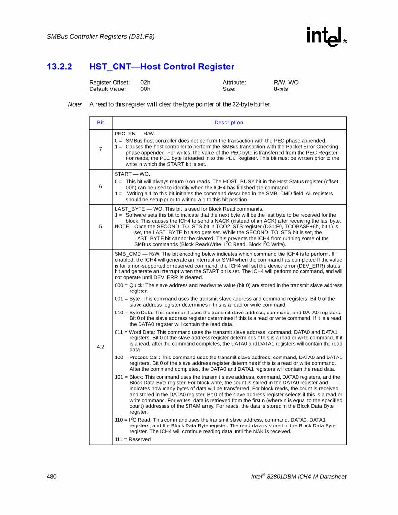
480 Intel® 82801DBM ICH4-M Datasheet
SMBus Controller Registers (D31:F3)
13.2.2 HST_CNT�Host Control RegisterRegister Offset: 02h Attribute: R/W, WODefault Value: 00h Size: 8-bits
Note: A read to this register will clear the byte pointer of the 32-byte buffer.
Bit Description
7
PEC_EN � R/W. 0 = SMBus host controller does not perform the transaction with the PEC phase appended.1 = Causes the host controller to perform the SMBus transaction with the Packet Error Checking
phase appended. For writes, the value of the PEC byte is transferred from the PEC Register. For reads, the PEC byte is loaded in to the PEC Register. This bit must be written prior to the write in which the START bit is set.
6
START � WO. 0 = This bit will always return 0 on reads. The HOST_BUSY bit in the Host Status register (offset
00h) can be used to identify when the ICH4 has finished the command.1 = Writing a 1 to this bit initiates the command described in the SMB_CMD field. All registers
should be setup prior to writing a 1 to this bit position.
5
LAST_BYTE � WO. This bit is used for Block Read commands.1 = Software sets this bit to indicate that the next byte will be the last byte to be received for the
block. This causes the ICH4 to send a NACK (instead of an ACK) after receiving the last byte.NOTE: Once the SECOND_TO_STS bit in TCO2_STS register (D31:F0, TCOBASE+6h, bit 1) is
set, the LAST_BYTE bit also gets set. While the SECOND_TO_STS bit is set, the LAST_BYTE bit cannot be cleared. This prevents the ICH4 from running some of the SMBus commands (Block Read/Write, I2C Read, Block I2C Write).
4:2
SMB_CMD � R/W. The bit encoding below indicates which command the ICH4 is to perform. If enabled, the ICH4 will generate an interrupt or SMI# when the command has completed If the value is for a non-supported or reserved command, the ICH4 will set the device error (DEV_ERR) status bit and generate an interrupt when the START bit is set. The ICH4 will perform no command, and will not operate until DEV_ERR is cleared.000 = Quick: The slave address and read/write value (bit 0) are stored in the transmit slave address
register.001 = Byte: This command uses the transmit slave address and command registers. Bit 0 of the
slave address register determines if this is a read or write command.010 = Byte Data: This command uses the transmit slave address, command, and DATA0 registers.
Bit 0 of the slave address register determines if this is a read or write command. If it is a read, the DATA0 register will contain the read data.
011 = Word Data: This command uses the transmit slave address, command, DATA0 and DATA1 registers. Bit 0 of the slave address register determines if this is a read or write command. If it is a read, after the command completes, the DATA0 and DATA1 registers will contain the read data.
100 = Process Call: This command uses the transmit slave address, command, DATA0 and DATA1 registers. Bit 0 of the slave address register determines if this is a read or write command. After the command completes, the DATA0 and DATA1 registers will contain the read data.
101 = Block: This command uses the transmit slave address, command, DATA0 registers, and the Block Data Byte register. For block write, the count is stored in the DATA0 register and indicates how many bytes of data will be transferred. For block reads, the count is received and stored in the DATA0 register. Bit 0 of the slave address register selects if this is a read or write command. For writes, data is retrieved from the first n (where n is equal to the specified count) addresses of the SRAM array. For reads, the data is stored in the Block Data Byte register.
110 = I2C Read: This command uses the transmit slave address, command, DATA0, DATA1 registers, and the Block Data Byte register. The read data is stored in the Block Data Byte register. The ICH4 will continue reading data until the NAK is received.
111 = Reserved

Intel® 82801DBM ICH4-M Datasheet 481
SMBus Controller Registers (D31:F3)
13.2.3 HST_CMD�Host Command RegisterRegister Offset: 03h Attribute: R/WDefault Value: 00h Size: 8 bits
13.2.4 XMIT_SLVA�Transmit Slave Address RegisterRegister Offset: 04h Attribute: R/WDefault Value: 00h Size: 8 bits
This register is transmitted by the host controller in the slave address field of the SMBus protocol.
13.2.5 HST_D0�Data 0 RegisterRegister Offset: 05h Attribute: R/WDefault Value: 00h Size: 8 bits
1
KILL � R/W. 0 = Normal SMBus Host Controller functionality.1 = When set, kills the current host transaction taking place, sets the FAILED status bit, and
asserts the interrupt (or SMI#). This bit, once set, must be cleared by software to allow the SMBus Host Controller to function normally.
0INTREN � R/W. 0 = Disable.1 = Enable the generation of an interrupt or SMI# upon the completion of the command.
Bit Description
Bit Description
7:0 This 8-bit field is transmitted by the host controller in the command field of the SMBus protocol during the execution of any command.
Bit Description
7:1 ADDRESS � R/W. 7-bit address of the targeted slave.
0RW � R/W. Direction of the host transfer.0 = Write1 = Read
Bit Description
7:0DATA0/COUNT � R/W. This field contains the eight bit data sent in the DATA0 field of the SMBus protocol. For block write commands, this register reflects the number of bytes to transfer. This register should be programmed to a value between 1 and 32 for block counts. A count of 0 or a count above 32 will result in unpredictable behavior. The host controller does not check or log illegal block counts.

482 Intel® 82801DBM ICH4-M Datasheet
SMBus Controller Registers (D31:F3)
13.2.6 HST_D1�Data 1 RegisterRegister Offset: 06h Attribute: R/WDefault Value: 00h Size: 8 bits
13.2.7 Host_BLOCK_DB�Host Block Data Byte RegisterRegister Offset: 07h Attribute: R/WDefault Value: 00h Size: 8 bits
13.2.8 PEC�Packet Error Check (PEC) RegisterRegister Offset: 08h Attribute: R/WDefault Value: 00h Size: 8 bits
Bit Description
7:0 DATA1 � R/W. This eight bit register is transmitted in the DATA1 field of the SMBus protocol during the execution of any command.
Bit Description
7:0
Block Data (BDTA)� R/W. This is either a register, or a pointer into a 32-byte block array, depending upon whether the E32B bit is set in the Auxiliary Control register. When the E32B bit is cleared, this is a register containing a byte of data to be sent on a block write or read from on a block read, just as it behaved on the ICH3.When the E32B bit is set, reads and writes to this register are used to access the 32-byte block data storage array. An internal index pointer is used to address the array, which is reset to 0 by reading the HCTL register (offset 02h). The index pointer then increments automatically upon each access to this register. The transfer of block data into (read) or out of (write) this storage array during an SMBus transaction always starts at index address 0.When the E2B bit is set, for writes, software will write up to 32-bytes to this register as part of the setup for the command. After the Host Controller has sent the Address, Command, and Byte Count fields, it will send the bytes in the SRAM pointed to by this register. After the byte count has been exhausted, the controller will set the DONE_STS bit (see definition above).When the E2B bit is cleared for writes, software will place a single byte in this register. After the host controller has sent the address, command, and byte count fields, it will send the byte in this register. If there is more data to send, software will write the next series of bytes to the SRAM pointed to by this register and clear the DONE_STS bit. The controller will then send the next byte. During the time between the last byte being transmitted to the next byte being transmitted, the controller will insert wait-states on the interface. When the E2B bit is set for reads, after receiving the byte count into the Data0 register, the first series of data bytes go into the SRAM pointed to by this register. If the byte count has been exhausted or the 32-byte SRAM has been filled, the controller will generate an SMI# or interrupt (depending on configuration) and set the DONE_STS bit. Software will then read the data. During the time between when the last byte is read from the SRAM to when the DONE_STS bit is cleared, the controller will insert wait-states on the interface.
Bit Description
7:0
PEC_DATA � R/W. This 8-bit register is written with the 8-bit CRC value that is used as the SMBus PEC data prior to a write transaction. For read transactions, the PEC data is loaded from the SMBus into this register and is then read by software. Software must ensure that the INUSE_STS bit is properly maintained to avoid having this field over-written by a write transaction following a read transaction.

Intel® 82801DBM ICH4-M Datasheet 483
SMBus Controller Registers (D31:F3)
13.2.9 RCV_SLVA�Receive Slave Address RegisterRegister Offset: 09h Attribute: R/WDefault Value: 44h Size: 8 bitsLockable: No Power Well: Resume
13.2.10 SLV_DATA�Receive Slave Data RegisterRegister Offset: 0Ah Attribute: RODefault Value: 0000h Size: 16 bitsLockable: No Power Well: Resume
This register contains the 16-bit data value written by the external SMBus master. The processor can then read the value from this register. This register is reset by RSMRST#, but not PCIRST#.
.
13.2.11 AUX_STS�Auxiliary Status RegisterRegister Offset: 0Ch Attribute: RW/CDefault Value: 00h Size: 8 bitsLockable: No Power Well: Resume
.
Bit Description
7 Reserved
6:0SLAVE_ADDR � R/W. This field is the slave address that the ICH4 decodes for read and write cycles. the default is not 0, so the SMBus Slave Interface can respond even before the processor comes up (or if the processor is dead). This register is cleared by RSMRST#, but not by PCIRST#.
Bit Description
15:8 Data Message Byte 1 (DATA_MSG1) � RO. See Section 5.18.7 for a discussion of this field.
7:0 Data Message Byte 0 (DATA_MSG0) � RO. See Section 5.18.7 for a discussion of this field.
Bit Description
7:1 Reserved
0
CRC Error (CRCE) � R/WC. 0 = Software clears this bit by writing a 1 to it. 1 = This bit is set if a received message contained a CRC error. When this bit is set, the DERR bit of
the host status register will also be set. This bit will be set by the controller if a software abort occurs in the middle of the CRC portion of the cycle or an abort happens after the ICH4 has received the final data bit transmitted by an external slave.

484 Intel® 82801DBM ICH4-M Datasheet
SMBus Controller Registers (D31:F3)
13.2.12 AUX_CTL�Auxiliary Control RegisterRegister Offset: 0Dh Attribute: R/WDefault Value: 00h Size: 8 bitsLockable: No Power Well: Resume
.
13.2.13 SMLINK_PIN_CTL�SMLink Pin Control RegisterRegister Offset: 0Eh Attribute: R/W, RODefault Value: See below Size: 8 bits
Note: This register is in the resume well and is reset by RSMRST#.
Bit Description
7:2 Reserved
1
Enable 32-byte Buffer (E32B)� R/W. 0 = Disable.1 = Enable. The Host Block Data register is a pointer into a 32-byte buffer, as opposed to a single
register. This enables the block commands to transfer or receive up to 32-bytes before the ICH4 generates an interrupt.
0
Automatically Append CRC (AAC) � R/W. 0 = Disable.1 = Enable. The ICH4 automatically appends the CRC. This bit must not be changed during SMBus
transactions, or undetermined behavior will result
Bit Description
7:3 Reserved
2
SMLINK_CLK_CTL � R/W. 0 = ICH4 drives the SMLINK[0] pin low, independent of what the other SMLINK logic would otherwise
indicate for the SMLINK[0] pin.1 = The SMLINK[0] pin is not overdriven low. The other SMLINK logic controls the state of the pin.
(Default)
1
SMLINK1_CUR_STS � R/W. This pin returns the value on the SMLINK[1] pin. This allows software to read the current state of the pin. Default value is dependent on an external signal level. 0 = Low1 = High
0
SMLINK0_CUR_STS � RO. This pin returns the value on the SMLINK[0] pin. This allows software to read the current state of the pin. Default value is dependent on an external signal level. 0 = Low1 = High

Intel® 82801DBM ICH4-M Datasheet 485
SMBus Controller Registers (D31:F3)
13.2.14 SMBUS_PIN_CTL�SMBUS Pin Control RegisterRegister Offset: 0Fh Attribute: R/W, RODefault Value: See below Size: 8 bits
Note: This register is in the resume well and is reset by RSMRST#.
13.2.15 SLV_STS�Slave Status RegisterRegister Offset: 10h Attribute: R/WCDefault Value: 00h Size: 8 bits
Note: This register is in the resume well and is reset by RSMRST#.
All bits in this register are implemented in the 64 kHz clock domain. Therefore, software must poll this register until a write takes effect before assuming that a write has completed internally.
Bit Description
7:3 Reserved
2
SMBCLK_CTL � R/W. 0 = ICH4 will drive the SMBCLK pin low, independent of what the other SMB logic would otherwise
indicate for the SMBCLK pin.1 = The SMBCLK pin is not overdriven low. The other SMBus logic controls the state of the pin.
(Default)
1
SMBDATA_CUR_STS � RO. This pin returns the value on the SMBDATA pin. This allows software to read the current state of the pin. Default value is dependent on an external signal level. 0 = Low1 = High
0
SMBCLK_CUR_STS � RO. This pin returns the value on the SMBCLK pin. This allows software to read the current state of the pin. Default value is dependent on an external signal level. 0 = Low1 = High
Bit Description
7:1 Reserved
0
HOST_NOTIFY_STS � R/WC. The ICH4 sets this bit to a 1 when it has completely received a successful Host Notify Command on the SMLink pins. Software reads this bit to determine that the source of the interrupt or SMI# was the reception of the Host Notify Command. Software clears this bit after reading any information needed from the Notify address and data registers by writing a 1 to this bit. Note that the ICH4 will allow the Notify Address and Data registers to be over-written once this bit has been cleared. When this bit is 1, the ICH4 will NACK the first byte (host address) of any new �Host Notify� commands on the SMLink. Writing a 0 to this bit has no effect.

486 Intel® 82801DBM ICH4-M Datasheet
SMBus Controller Registers (D31:F3)
13.2.16 SLV_CMD�Slave Command RegisterRegister Offset: 11h Attribute: R/WDefault Value: 00h Size: 8 bits
Note: This register is in the resume well and is reset by RSMRST#
13.2.17 NOTIFY_DADDR�Notify Device AddressRegister Offset: 14h Attribute: RODefault Value: 00h Size: 8 bits
Note: This register is in the resume well and is reset by RSMRST#
Bit Description
7:2 Reserved
2
SMBALERT_DIS � R/W.0 = Allows the generation of the interrupt or SMI#.1 = Software sets this bit to block the generation of the interrupt or SMI# due to the SMBALERT#
source. This bit is logically inverted and ANDed with the SMBALERT_STS bit. The resulting signal is distributed to the SMI# and/or interrupt generation logic. This bit does not effect the wake logic.
1
HOST_NOTIFY_WKEN � R/W. 0 = Disable.1 = Enables the reception of a Host Notify command as a wake event. When enabled this event is
�OR�ed in with the other SMBus wake events and is reflected in the SMB_WAK_STS bit of the General Purpose Event 0 Status register.
0
HOST_NOTIFY_INTREN � R/W. 0 = Disable1 = Enables the generation of interrupt or SMI# when HOST_NOTIFY_STS is 1. This enable does
not affect the setting of the HOST_NOTIFY_STS bit. When the interrupt is generated, either PIRQ[B]# or SMI# is generated, depending on the value of the SMB_SMI_EN bit (D31, F3, Off40h, B1). If the HOST_NOTIFY_STS bit is set when this bit is written to a 1, then the interrupt (or SMI#) will be generated. The interrupt (or SMI#) is logically generated by AND�ing the STS and INTREN bits.
Bit Description
7:1DEVICE_ADDRESS � RO. This field contains the 7-bit device address received during the Host Notify protocol of the SMBus 2.0 Specification. Software should only consider this field valid when the HOST_NOTIFY_STS bit is set to 1.
0 Reserved

Intel® 82801DBM ICH4-M Datasheet 487
SMBus Controller Registers (D31:F3)
13.2.18 NOTIFY_DLOW�Notify Data Low Byte RegisterRegister Offset: 16h Attribute: RODefault Value: 00h Size: 8 bits
Note: This register is in the resume well and is reset by RSMRST#
13.2.19 NOTIFY_DHIGH�Notify Data High Byte RegisterRegister Offset: 17h Attribute: RODefault Value: 00h Size: 8 bits
Note: This register is in the resume well and is reset by RSMRST#
Bit Description
7:0DATA_LOW_BYTE � RO. This field contains the first (low) byte of data received during the Host Notify protocol of the SMBus 2.0 Specification. Software should only consider this field valid when the HOST_NOTIFY_STS bit is set to 1.
Bit Description
7:0DATA_HIGH_BYTE � RO. This field contains the second (high) byte of data received during the Host Notify protocol of the SMBus 2.0 Specification. Software should only consider this field valid when the HOST_NOTIFY_STS bit is set to 1.

488 Intel® 82801DBM ICH4-M Datasheet
SMBus Controller Registers (D31:F3)
This page is intentionally left blank.
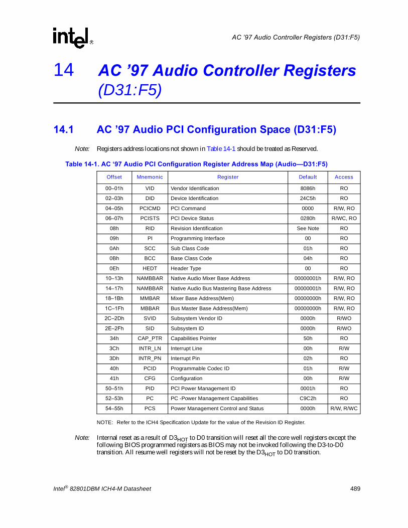
Intel® 82801DBM ICH4-M Datasheet 489
AC �97 Audio Controller Registers (D31:F5)
14 AC �97 Audio Controller Registers (D31:F5)
14.1 AC �97 Audio PCI Configuration Space (D31:F5)Note: Registers address locations not shown in Table 14-1 should be treated as Reserved.
NOTE: Refer to the ICH4 Specification Update for the value of the Revision ID Register.
Note: Internal reset as a result of D3HOT to D0 transition will reset all the core well registers except the following BIOS programmed registers as BIOS may not be invoked following the D3-to-D0 transition. All resume well registers will not be reset by the D3HOT to D0 transition.
Table 14-1. AC �97 Audio PCI Configuration Register Address Map (Audio�D31:F5)
Offset Mnemonic Register Default Access
00�01h VID Vendor Identification 8086h RO
02�03h DID Device Identification 24C5h RO
04�05h PCICMD PCI Command 0000 R/W, RO
06�07h PCISTS PCI Device Status 0280h R/WC, RO
08h RID Revision Identification See Note RO
09h PI Programming Interface 00 RO
0Ah SCC Sub Class Code 01h RO
0Bh BCC Base Class Code 04h RO
0Eh HEDT Header Type 00 RO
10�13h NAMBBAR Native Audio Mixer Base Address 00000001h R/W, RO
14�17h NAMBBAR Native Audio Bus Mastering Base Address 00000001h R/W, RO
18�1Bh MMBAR Mixer Base Address(Mem) 00000000h R/W, RO
1C�1Fh MBBAR Bus Master Base Address(Mem) 00000000h R/W, RO
2C�2Dh SVID Subsystem Vendor ID 0000h R/WO
2E�2Fh SID Subsystem ID 0000h R/WO
34h CAP_PTR Capabilities Pointer 50h RO
3Ch INTR_LN Interrupt Line 00h R/W
3Dh INTR_PN Interrupt Pin 02h RO
40h PCID Programmable Codec ID 01h R/W
41h CFG Configuration 00h R/W
50�51h PID PCI Power Management ID 0001h RO
52�53h PC PC -Power Management Capabilities C9C2h RO
54�55h PCS Power Management Control and Status 0000h R/W, R/WC

490 Intel® 82801DBM ICH4-M Datasheet
AC �97 Audio Controller Registers (D31:F5)
Core Well registers not reset by the D3HOT to D0 transition:
� offset 2Ch�2Dh: Subsystem Vendor ID (SVID)
� offset 2Eh�2Fh: Subsystem ID (SID)
� offset 40h: Programmable Codec ID (PCID)
� offset 41h: Configuration (CFG)
Resume Well registers will NOT be reset by the D3HOT to D0 transition:
� offset 54h�55h: Power Management Control and Status (PCS)
� Bus Mastering Register: Global Status Register, bits 17:16
� Bus Mastering Register: SDATA_IN MAP register, bits 7:3
14.1.1 VID�Vendor Identification Register (Audio�D31:F5)Offset: 00�01h Attribute: RODefault Value: 8086h Size: 16 BitsLockable: No Power Well: Core
14.1.2 DID�Device Identification Register (Audio�D31:F5)Offset: 02�03h Attribute: RODefault Value: 24C5h Size: 16 BitsLockable: No Power Well: Core
Bit Description
15:0 Vendor Identification Value � RO. This is a 16-bit value assigned to Intel.
Bit Description
15:0 Device Identification Value � RO.
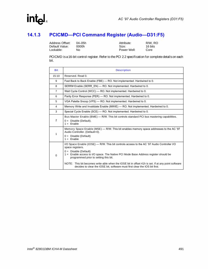
Intel® 82801DBM ICH4-M Datasheet 491
AC �97 Audio Controller Registers (D31:F5)
14.1.3 PCICMD�PCI Command Register (Audio�D31:F5)Address Offset: 04�05h Attribute: R/W, RODefault Value: 0000h Size: 16 bitsLockable: No Power Well: Core
PCICMD is a 16-bit control register. Refer to the PCI 2.2 specification for complete details on each bit.
Bit Description
15:10 Reserved. Read 0.
9 Fast Back to Back Enable (FBE) � RO. Not implemented. Hardwired to 0.
8 SERR# Enable (SERR_EN) � RO. Not implemented. Hardwired to 0.
7 Wait Cycle Control (WCC) � RO. Not implemented. Hardwired to 0.
6 Parity Error Response (PER) � RO. Not implemented. Hardwired to 0.
5 VGA Palette Snoop (VPS) � RO. Not implemented. Hardwired to 0.
4 Memory Write and Invalidate Enable (MWIE) � RO. Not implemented. Hardwired to 0.
3 Special Cycle Enable (SCE) � RO. Not implemented. Hardwired to 0.
2Bus Master Enable (BME) � R/W. This bit controls standard PCI bus mastering capabilities.0 = Disable (Default).1 = Enable
1
Memory Space Enable (MSE) � R/W. This bit enables memory space addresses to the AC �97 Audio Controller. (Default=0).0 = Disable (Default)1 = Enable
0
I/O Space Enable (IOSE) � R/W. This bit controls access to the AC �97 Audio Controller I/O space registers. 0 = Disable (Default)1 = Enable access to I/O space. The Native PCI Mode Base Address register should be
programmed prior to setting this bit.
NOTE: This bit becomes write-able when the IOSE bit in offset 41h is set. If at any point software decides to clear the IOSE bit, software must first clear the IOS bit first.

492 Intel® 82801DBM ICH4-M Datasheet
AC �97 Audio Controller Registers (D31:F5)
14.1.4 PCISTS�PCI Device Status Register (Audio�D31:F5)Offset: 06�07h Attribute: R/WC, RODefault Value 0280h Size: 16 bitsLockable: No Power Well: Core
PCISTA is a 16-bit status register. Refer to the PCI 2.2 specification for complete details on each bit.
Bit Description
15 Detected Parity Error (DPE) � RO. Not implemented. Hardwired to 0.
14 Signaled System Error (SSE) � RO. Not implemented. Hardwired to 0.
13Master Abort Status (MAS) � R/WC.0 = Software clears this bit by writing a 1 to the bit position.1 = Bus Master AC '97 2.3 interface function, as a master, generates a master abort.
12 Reserved. Will always read as 0.
11 Signaled Target Abort (STA) � RO. Not implemented. Hardwired to 0.
10:9DEVSEL# Timing Status (DEV_STS) � RO. This 2-bit field reflects the ICH4's DEVSEL# timing when performing a positive decode. 01b = Medium timing.
8 Data Parity Error Detected (DPED) � RO. Not implemented. Hardwired to 0.
7 Fast Back to Back Capable (FB2BC) � RO. Hardwired to 1. This bit indicates that the ICH4 as a target is capable of fast back-to-back transactions.
6 User Definable Features (UDF) � RO. Not implemented. Hardwired to 0.
5 66 MHz Capable (66MHZ_CAP) � RO. Hardwired to 0.
4 Capabilities List (CLIST) � RO. Indicates that the controller contains a capabilities pointer list. The first item is pointed to by looking at configuration offset 34h.
3:0 Reserved.

Intel® 82801DBM ICH4-M Datasheet 493
AC �97 Audio Controller Registers (D31:F5)
14.1.5 RID�Revision Identification Register (Audio�D31:F5)Offset: 08h Attribute: RODefault Value: See Bit Description Size: 8 BitsLockable: No Power Well: Core
14.1.6 PI�Programming Interface Register (Audio�D31:F5)Offset: 09h Attribute: RODefault Value: 00h Size: 8 bitsLockable: No Power Well: Core
14.1.7 SCC�Sub Class Code Register (Audio�D31:F5)Address Offset: 0Ah Attribute: RODefault Value: 01h Size: 8 bitsLockable: No Power Well: Core
14.1.8 BCC�Base Class Code Register (Audio�D31:F5)Address Offset: 0Bh Attribute: RODefault Value: 04h Size: 8 bitsLockable: No Power Well: Core
Bit Description
7:0 Revision Identification Value � RO. Refer to the ICH4 Specification Update for the value of the Revision ID Register.
Bit Description
7:0 Programming Interface � RO.
Bit Description
7:0Sub Class Code � RO. 01h = Audio Device
Bit Description
7:0Base Class Code � RO.04h = Multimedia device

494 Intel® 82801DBM ICH4-M Datasheet
AC �97 Audio Controller Registers (D31:F5)
14.1.9 HEDT�Header Type Register (Audio�D31:F5)Address Offset: 0Eh Attribute: RODefault Value: 00h Size: 8 bitsLockable: No Power Well: Core
14.1.10 NAMBAR�Native Audio Mixer Base Address Register (Audio�D31:F5)Address Offset: 10�13h Attribute: R/W, RODefault Value: 00000001h Size: 32 bitsLockable: No Power Well: Core
The Native PCI Mode Audio function uses PCI Base Address register #1 to request a contiguous block of I/O space that is to be used for the Native Audio Mixer software interface. The mixer requires 256 bytes of I/O space. Native Audio Mixer and Modem codec I/O registers are located from 00h to 7Fh and reside in the codec. Access to these registers will be decoded by the AC '97 controller and forwarded over the AC-link to the codec. The codec will then respond with the register value.
In the case of the split codec implementation, accesses to the different codecs are differentiated by the controller by using address offsets 00h�7Fh for the primary codec and address offsets 80h�FEh for the secondary codec.
Note: The tertiary codec cannot be addressed via this address space. The tertiary space is only available from the new MMBAR register. This register powers up as read only and only becomes writeable when the IOSE bit in offset 41h is set.
For description of these I/O registers, refer to the Audio Codec �97 Component Specification, Version 2.3.
Bit Description
7:0 Header Type � RO. Hardwired to 00h.
Bit Description
31:16 Hardwired to 0s
15:8
Base Address � R/W. These bits are used in the I/O space decode of the Native Audio Mixer interface registers. The number of upper bits that a device actually implements depends on how much of the address space the device will respond to. For the AC �97 mixer, the upper 16 bits are hardwired to 0, while bits 15:8 are programmable. This configuration yields a maximum I/O block size of 256 bytes for this base address.
7:1 Reserved. Read as 0s.
0 Resource Type Indicator (RTE) � RO. Hardwired to 1, indicating a request for I/O space.

Intel® 82801DBM ICH4-M Datasheet 495
AC �97 Audio Controller Registers (D31:F5)
14.1.11 NABMBAR�Native Audio Bus Mastering Base Address Register (Audio�D31:F5)Address Offset: 14�17h Attribute: R/W, RODefault Value: 00000001h Size: 32 bitsLockable: No Power Well: Core
The Native PCI Mode Audio function uses PCI Base Address register #1 to request a contiguous block of I/O space that is to be used for the Native Mode Audio software interface.
Note: The DMA registers for S/PDIF and Microphone In 2 cannot be addressed via this address space. These DMA functions are only available from the new MBBAR register. This register powers up as read only and only becomes write-able when the IOSE bit in offset 41h is set.
14.1.12 MMBAR�Mixer Base Address Register (Audio�D31:F5)Address Offset: 18�1Bh Attribute: R/W, RODefault Value: 00000000h Size: 32 bitsLockable: No Power Well: Core
This BAR creates 512 bytes of memory space to signify the base address of the register space. The lower 256 bytes of this space map to the same registers as the 256-byte I/O space pointed to by NAMBAR. The lower 384 bytes are divided as follows:
� 128 bytes for the primary codec (offsets 00�7Fh)
� 128 bytes for the secondary codec (offsets 80�FFh)
� 128 bytes for the tertiary codec (offsets 100�17Fh).
� 128 bytes of reserved space (offsets 180�1FFh), returning all 0s.
Bit Description
31:16 Hardwired to 0s
15:6
Base Address � R/W. These bits are used in the I/O space decode of the Native Audio Bus Mastering interface registers. The number of upper bits that a device actually implements depends on how much of the address space the device will respond to. For AC '97 bus mastering, the upper 16 bits are hardwired to 0, while bits 15:6 are programmable. This configuration yields a maximum I/O block size of 64 bytes for this base address.
5:1 Reserved. Read as 0s.
0 Resource Type Indicator (RTE) � RO. This bit is set to 0, indicating a request for I/O space.
Bit Description
31:9 Base Address � R/W Lower 32-bits of the 512-byte memory offset to use for decoding the primary, secondary, and tertiary codec�s mixer spaces.
8:3 Reserved. Read as 0s.
2:1 Type � RO. Indicates the base address exists in 32-bit address space
0 Resource Type Indicator (RTE) � RO. Hardwired to 0, indicating a request for memory space.

496 Intel® 82801DBM ICH4-M Datasheet
AC �97 Audio Controller Registers (D31:F5)
14.1.13 MBBAR�Bus Master Base Address Register (Audio�D31:F5)Address Offset: 1C�1Fh Attribute: R/W, RODefault Value: 00000000h Size: 32 bitsLockable: No Power Well: Core
This BAR creates 256-bytes of memory space to signify the base address of the bus master memory space. The lower 64-bytes of the space pointed to by this register point to the same registers as the MBBAR.
14.1.14 SVID�Subsystem Vendor ID Register (Audio�D31:F5)Address Offset: 2D�2Ch Attribute: R/WODefault Value: 0000h Size: 16 bitsLockable: No Power Well: Core
The SVID register, in combination with the Subsystem ID register, enable the operating environment to distinguish one audio subsystem from the other(s). This register is implemented as write-once register. Once a value is written to it, the value can be read back. Any subsequent writes will have no effect.
This register is not affected by the D3HOT to D0 transition.
Bit Description
31:8 Base Address � R/W. I/O offset to use for decoding the PCM In, PCM Out, and Microphone 1 DMA engines.
7:3 Reserved. Read as 0s.
2:1 Type � RO. Indicates the base address exists in 32-bit address space
0 Resource Type Indicator (RTE) � RO. This bit is set to 0, indicating a request for memory space.
Bit Description
15:0 Subsystem Vendor ID � R/Write-Once.

Intel® 82801DBM ICH4-M Datasheet 497
AC �97 Audio Controller Registers (D31:F5)
14.1.15 SID�Subsystem ID Register (Audio�D31:F5)Address Offset: 2E�2Fh Attribute: R/WODefault Value: 0000h Size: 16 bitsLockable: No Power Well: Core
The SID register, in combination with the Subsystem Vendor ID register make it possible for the operating environment to distinguish one audio subsystem from the other(s). This register is implemented as write-once register. Once a value is written to it, the value can be read back. Any subsequent writes will have no effect. This register is not affected by the D3HOT to D0 transition.
T
14.1.16 CAP_PTR�Capabilities Pointer Register (Audio�D31:F5)Address Offset: 34h Attribute: RODefault Value: 50h Size: 8 bitsLockable: No Power Well: Core
This register indicates the offset for the capability pointer.
14.1.17 INTR_LN�Interrupt Line Register (Audio�D31:F5)Address Offset: 3Ch Attribute: R/WDefault Value: 00h Size: 8 bitsLockable: No Power Well: Core
This register indicates which PCI interrupt line is used for the AC �97 module interrupt.
Bit Description
15:0 Subsystem ID � R/Write-Once.
Bit Description
7:0 Capabilities Pointer (CAP_PTR) � RO. This field indicates that the first capability pointer offset is offset 50h
Bit Description
7:0 Interrupt Line (INT_LN) � R/W. This data is not used by the ICH4. It is used to communicate to software the interrupt line that the interrupt pin is connected to.
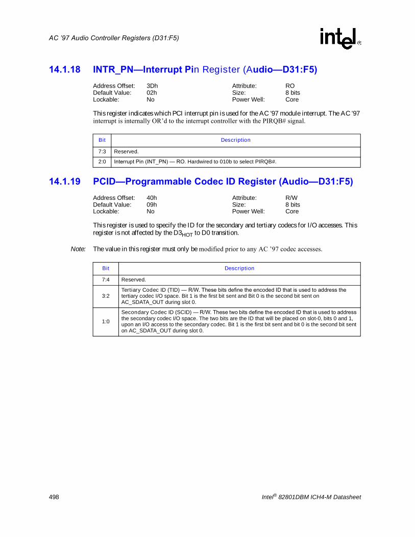
498 Intel® 82801DBM ICH4-M Datasheet
AC �97 Audio Controller Registers (D31:F5)
14.1.18 INTR_PN�Interrupt Pin Register (Audio�D31:F5)Address Offset: 3Dh Attribute: RODefault Value: 02h Size: 8 bitsLockable: No Power Well: Core
This register indicates which PCI interrupt pin is used for the AC '97 module interrupt. The AC '97 interrupt is internally OR�d to the interrupt controller with the PIRQB# signal.
14.1.19 PCID�Programmable Codec ID Register (Audio�D31:F5)Address Offset: 40h Attribute: R/WDefault Value: 09h Size: 8 bitsLockable: No Power Well: Core
This register is used to specify the ID for the secondary and tertiary codecs for I/O accesses. This register is not affected by the D3HOT to D0 transition.
Note: The value in this register must only be modified prior to any AC �97 codec accesses.
Bit Description
7:3 Reserved.
2:0 Interrupt Pin (INT_PN) � RO. Hardwired to 010b to select PIRQB#.
Bit Description
7:4 Reserved.
3:2Tertiary Codec ID (TID) � R/W. These bits define the encoded ID that is used to address the tertiary codec I/O space. Bit 1 is the first bit sent and Bit 0 is the second bit sent on AC_SDATA_OUT during slot 0.
1:0
Secondary Codec ID (SCID) � R/W. These two bits define the encoded ID that is used to address the secondary codec I/O space. The two bits are the ID that will be placed on slot-0, bits 0 and 1, upon an I/O access to the secondary codec. Bit 1 is the first bit sent and bit 0 is the second bit sent on AC_SDATA_OUT during slot 0.

Intel® 82801DBM ICH4-M Datasheet 499
AC �97 Audio Controller Registers (D31:F5)
14.1.20 CFG�Configuration Register (Audio�D31:F5)Address Offset: 41h Attribute: R/WDefault Value: 00h Size: 8 bitsLockable: No Power Well: Core
This register is used to specify the ID for the secondary and tertiary codecs for I/O accesses. This register is not affected by the D3HOT to D0 transition.
14.1.21 PID�PCI Power Management Capability ID Register (Audio�D31:F5)Address Offset: 50h Attribute: RODefault Value: 0001h Size: 16 bitsLockable: No Power Well: Core
14.1.22 PC�Power Management Capabilities Register (Audio�D31:F5)Address Offset: 52h Attribute: RODefault Value: C9C2h Size: 16 bitsLockable: No Power Well: Core
This register is not affected by the D3HOT to D0 transition.
Bit Description
7:1 Reserved � RO.
0
I/O Space Enable (IOSE) � R/W. 0 = Disable. The IOS bit at offset 04h and the I/O space BARs at offset 10h and 14h become read
only registers. (Default)1 = Enable. BIOS must explicitly set this bit to allow a legacy driver to work.
Bit Description
15:8 Next Capability (NEXT) � RO. This field indicates that the next item in the list is at offset 00h.
7:0 Capability ID (CAP) � RO. This field indicates that this pointer is a message signaled interrupt capability.
Bit Description
15:11 PME Support � RO. This field indicates PME# can be generated from all D states.
10:9 Reserved.
8:6 Auxiliary Current � RO. This field reports 375 mA maximum Suspend well current required when in the D3cold state.
5 Device Specific Initialization (DSI) � RO. This bit indicates that no device-specific initialization is required.
4 Reserved � RO.
3 PME Clock � RO. This bit indicates that PCI clock is not required to generate PME#.
2:0 Version � RO. Indicates support for Revision 1.1 of the PCI Power Management Specification.

500 Intel® 82801DBM ICH4-M Datasheet
AC �97 Audio Controller Registers (D31:F5)
14.1.23 PCS�Power Management Control and Status Register (Audio�D31:F5)Address Offset: 54h Attribute: R/W, R/WCDefault Value: 0000h Size: 16 bitsLockable: No Power Well: Resume
Bit Description
15
PME Status (PMES) � RW/C. 0 = Software clears this bit by writing a 1 to it. 1 = This bit is set when the AC �97 controller would normally assert the PME# signal independent of
the state of the PME_En bit. This bit resides in the resume well.
14:9 Reserved � RO.
8
PME Enable (PMEE) � R/W. 0 = Disable.1 = Enable. When set, and if corresponding PMES is also set, the AC'97 controller sets the
AC97_STS bit in the GPE0_STS register
7:2 Reserved � RO.
1:0
Power State � R/W. This field is used both to determine the current power state of the AC �97 control-ler and to set a new power state. The values are:
00 = D0 state
01 = not supported
10 = not supported
11 = D3HOT state
When in the D3HOT state, the AC �97 controller�s configuration space is available, but the I/O and memory spaces are not. Additionally, interrupts are blocked.If software attempts to write a value of 10b or 01b in to this field, the write operation must complete normally; however, the data is discarded and no state change occurs.

Intel® 82801DBM ICH4-M Datasheet 501
AC �97 Audio Controller Registers (D31:F5)
14.2 AC �97 Audio I/O Space (D31:F5)The AC �97 I/O space includes Native Audio Bus Master Registers and Native Mixer Registers. For the ICH4, the offsets are important as they will determine bits[1:0] of the TAG field (codec ID).
Audio Mixer I/O space can be accessed as a 16-bit field only since the data packet length on AC-link is a word. Any S/W access to the codec will be done as a 16-bit access starting from the first active byte. In case no byte enables are active, the access will be done at the first word of the QWord that contains the address of this request.
Table 14-2. Intel® ICH4 Audio Mixer Register Configuration (Sheet 1 of 2)
Primary Offset(Codec ID =00)
Secondary Offset(Codec ID =01)
Tertiary Offset(Codec ID =10)
NAMBAR Exposed Registers (D31:F5)
00h 80h 100h Reset
02h 82h 102h Master Volume
04h 84h 104h Aux Out Volume
06h 86h 106h Mono Volume
08h 88h 108h Master Tone (R & L)
0Ah 8Ah 10Ah PC_BEEP Volume
0Ch 8Ch 10Ch Phone Volume
0Eh 8Eh 10Eh Mic Volume
10h 90h 110h Line In Volume
12h 92h 112h CD Volume
14h 94h 114h Video Volume
16h 96h 116h Aux In Volume
18h 98h 118h PCM Out Volume
1Ah 9Ah 11Ah Record Select
1Ch 9Ch 11Ch Record Gain
1Eh 9Eh 11Eh Record Gain Mic
20h A0h 120h General Purpose
22h A2h 122h 3D Control
24h A4h 124h AC �97 RESERVED
26h A6h 126h Powerdown Ctrl/Stat
28h A8h 128h Extended Audio
2Ah AAh 12Ah Extended Audio Ctrl/Stat
2Ch ACh 12Ch PCM Front DAC Rate
2Eh AEh 12Eh PCM Surround DAC Rate
30h B0h 130h PCM LFE DAC Rate
32h B2h 132h PCM LR ADC Rate
34h B4h 134h MIC ADC Rate
36h B6h 136h 6Ch Vol: C, LFE

502 Intel® 82801DBM ICH4-M Datasheet
AC �97 Audio Controller Registers (D31:F5)
NOTE:1. Software should not try to access reserved registers2. Primary Codec ID cannot be changed. Secondary codec ID can be changed via bits 1:0 of configuration
register 40h. Tertiary codec ID can be changed via bits 3:2 of configuration register 40h. 3. The tertiary offset is only available through the memory space defined by the MMBAR register.
The Bus Master registers are located from offset + 00h to offset + 51h and reside in the AC �97 controller. Accesses to these registers do NOT cause the cycle to be forwarded over the AC-link to the codec. Software can access these registers as bytes, word, or DWord quantities, but reads must not cross DWord boundaries.
In the case of the split codec implementation accesses to the different codecs are differentiated by the controller by using address offsets 00h � 7Fh for the primary codec, address offsets 80h � FFh for the secondary codec and address offsets 100h � 17Fh for the tertiary codec.
The Global Control (GLOB_CNT) and Global Status (GLOB_STA) registers are aliased to the same global registers in the audio and modem I/O space. Therefore a read/write to these registers in either audio or modem I/O space affects the same physical register.
Bus Mastering registers exist in I/O space and reside in the AC �97 controller. The six channels, PCM in, PCM in 2, PCM out, Mic in, Mic 2, and S/PDIF out, each have their own set of Bus Mastering registers. The following register descriptions apply to all six channels. The register definition section titles use a generic �x_� in front of the register to indicate that the register applies to all six channels. The naming prefix convention used in Table 14-3 and in the register description I/O address is as follows:
PI = PCM in channelPO = PCM out channelMC = Mic in channel.MC2 = Mic 2 channelPI2 = PCM in 2 channelSP = S/PDIF out channel.
38h B8h 138h 6Ch Vol: L, R Surround
3Ah BAh 13Ah S/PDIF Control
3C�56h BC�D6h 13C�156h Intel RESERVED
58h D8h 158h AC �97 Reserved
5Ah DAh 15Ah Vendor Reserved
7Ch FCh 17Ch Vendor ID1
7Eh FEh 17Eh Vendor ID2
Table 14-2. Intel® ICH4 Audio Mixer Register Configuration (Sheet 2 of 2)
Primary Offset(Codec ID =00)
Secondary Offset(Codec ID =01)
Tertiary Offset(Codec ID =10)
NAMBAR Exposed Registers (D31:F5)
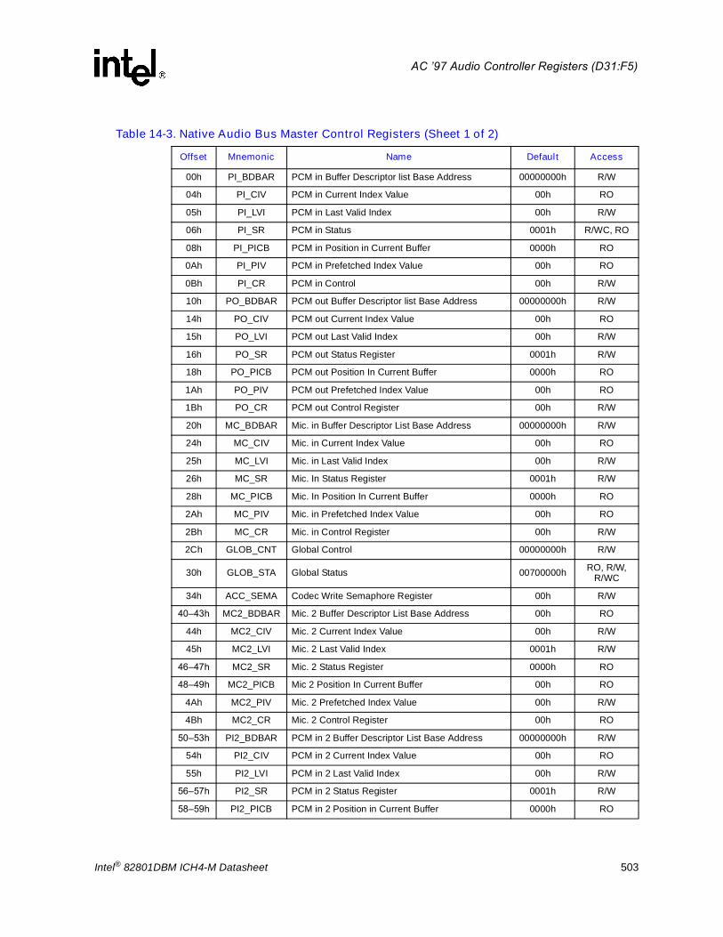
Intel® 82801DBM ICH4-M Datasheet 503
AC �97 Audio Controller Registers (D31:F5)
Table 14-3. Native Audio Bus Master Control Registers (Sheet 1 of 2)
Offset Mnemonic Name Default Access
00h PI_BDBAR PCM in Buffer Descriptor list Base Address 00000000h R/W
04h PI_CIV PCM in Current Index Value 00h RO
05h PI_LVI PCM in Last Valid Index 00h R/W
06h PI_SR PCM in Status 0001h R/WC, RO
08h PI_PICB PCM in Position in Current Buffer 0000h RO
0Ah PI_PIV PCM in Prefetched Index Value 00h RO
0Bh PI_CR PCM in Control 00h R/W
10h PO_BDBAR PCM out Buffer Descriptor list Base Address 00000000h R/W
14h PO_CIV PCM out Current Index Value 00h RO
15h PO_LVI PCM out Last Valid Index 00h R/W
16h PO_SR PCM out Status Register 0001h R/W
18h PO_PICB PCM out Position In Current Buffer 0000h RO
1Ah PO_PIV PCM out Prefetched Index Value 00h RO
1Bh PO_CR PCM out Control Register 00h R/W
20h MC_BDBAR Mic. in Buffer Descriptor List Base Address 00000000h R/W
24h MC_CIV Mic. in Current Index Value 00h RO
25h MC_LVI Mic. in Last Valid Index 00h R/W
26h MC_SR Mic. In Status Register 0001h R/W
28h MC_PICB Mic. In Position In Current Buffer 0000h RO
2Ah MC_PIV Mic. in Prefetched Index Value 00h RO
2Bh MC_CR Mic. in Control Register 00h R/W
2Ch GLOB_CNT Global Control 00000000h R/W
30h GLOB_STA Global Status 00700000h RO, R/W, R/WC
34h ACC_SEMA Codec Write Semaphore Register 00h R/W
40�43h MC2_BDBAR Mic. 2 Buffer Descriptor List Base Address 00h RO
44h MC2_CIV Mic. 2 Current Index Value 00h R/W
45h MC2_LVI Mic. 2 Last Valid Index 0001h R/W
46�47h MC2_SR Mic. 2 Status Register 0000h RO
48�49h MC2_PICB Mic 2 Position In Current Buffer 00h RO
4Ah MC2_PIV Mic. 2 Prefetched Index Value 00h R/W
4Bh MC2_CR Mic. 2 Control Register 00h RO
50�53h PI2_BDBAR PCM in 2 Buffer Descriptor List Base Address 00000000h R/W
54h PI2_CIV PCM in 2 Current Index Value 00h RO
55h PI2_LVI PCM in 2 Last Valid Index 00h R/W
56�57h PI2_SR PCM in 2 Status Register 0001h R/W
58�59h PI2_PICB PCM in 2 Position in Current Buffer 0000h RO

504 Intel® 82801DBM ICH4-M Datasheet
AC �97 Audio Controller Registers (D31:F5)
Note: Internal reset as a result of D3HOT to D0 transition will reset all the core well registers except the registers shared with the AC �97 Modem (GCR, GSR, CASR). All resume well registers will not be reset by the D3HOT to D0 transition.
Core Well registers and bits NOT reset by the D3HOT to D0 transition:
� offset 2Ch�2Fh � bits[6:0] Global Control (GLOB_CNT)
� offset 30h�33h � bits[29,15,11:10,0] Global Status (GLOB_STA)
� offset 34h � Codec Access Semaphore Register (CAS)
Resume Well registers and bits will NOT be reset by the D3HOT to D0 transition:
� offset 30h�33h � bits[17:16] Global Status (GLOB_STA)
14.2.1 x_BDBAR�Buffer Descriptor Base Address RegisterI/O Address: NABMBAR + 00h (PIBDBAR), Attribute: R/W
NABMBAR + 10h (POBDBAR),NABMBAR + 20h (MCBDBAR)MBBAR + 40h (MC2BDBAR)MBBAR + 50h (PI2BDBAR)MBBAR + 60h (SPBAR)
Default Value: 00000000h Size: 32 bitsLockable: No Power Well: Core
Software can read the register at offset 00h by performing a single 32 bit read from address offset 00h. Reads across DWord boundaries are not supported.
5Ah PI2_PIV PCM In 2 Prefetched Index Value 00h RO
5Bh PI2_CR PCM In 2 Control Register 00h R/W
60�63 SP_BAR S/PDIF Buffer Descriptor List Base Address 00000000h R/W
64h SP_CIV S/PDIF Current Index Value 00h RO
65h SP_LVI S/PDIF Last Valid Index 00h R/W
66�67h SP_SR S/PDIF Status Register 0001h R/W
68�69h SP_PICB S/PDIF Position In Current Buffer 0000h RO
6Ah SP_PIV S/PDIF Prefetched Index Value 00h RO
6Bh SP_CR S/PDIF Control Register 00h R/W
80h SDM SData_IN Map 00h R/W, RO
Table 14-3. Native Audio Bus Master Control Registers (Sheet 2 of 2)
Offset Mnemonic Name Default Access
Bit Description
31:3Buffer Descriptor Base Address [31:3] � R/W. These bits represent address bits 31:3. The data should be aligned on 8 byte boundaries. Each buffer descriptor is 8 bytes long and the list can contain a maximum of 32 entries.
2:0 Hardwired to 0.

Intel® 82801DBM ICH4-M Datasheet 505
AC �97 Audio Controller Registers (D31:F5)
14.2.2 x_CIV�Current Index Value RegisterI/O Address: NABMBAR + 04h (PICIV), Attribute: RO
NABMBAR + 14h (POCIV), NABMBAR + 24h (MCCIV)MBBAR + 44h (MC2CIV)MBBAR + 54h (PI2CIV)MBBAR + 64h (SPCIV)
Default Value: 00h Size: 8 bitsLockable: No Power Well: Core
Software can read the registers at offsets 04h, 05h and 06h simultaneously by performing a single 32 bit read from address offset 04h. Software can also read this register individually by doing a single 8 bit read to offset 04h. Reads across DWord boundaries are not supported.
14.2.3 x_LVI�Last Valid Index RegisterI/O Address: NABMBAR + 05h (PILVI), Attribute: R/W
NABMBAR + 15h (POLVI), NABMBAR + 25h (MCLVI)MBBAR + 45h (MC2LVI)MBBAR + 55h (PI2LVI)MBBAR + 65h (SPLVI)
Default Value: 00h Size: 8 bitsLockable: No Power Well: Core
Software can read the registers at offsets 04h, 05h and 06h simultaneously by performing a single 32-bit read from address offset 04h. Software can also read this register individually by doing a single 8 bit read to offset 05h. Reads across DWord boundaries are not supported.
Bit Description
7:5 Hardwired to 0
4:0Current Index Value [4:0] � RO. These bits represent which buffer descriptor within the list of 32 descriptors is currently being processed. As each descriptor is processed, this value is incremented. The value rolls over after it reaches 31.
Bit Description
7:5 Hardwired to 0.
4:0 Last Valid Index [4:0] � R/W. This field represents the last valid descriptor in the list. This value is updated by the software each time it prepares a new buffer and adds it to the list.

506 Intel® 82801DBM ICH4-M Datasheet
AC �97 Audio Controller Registers (D31:F5)
14.2.4 x_SR�Status RegisterI/O Address: NABMBAR + 06h (PISR), Attribute: R/WC, RO
NABMBAR + 16h (POSR), NABMBAR + 26h (MCSR)MBBAR + 46h (MC2SR)MBBAR + 56h (PI2SR)MBBAR + 66h (SPSR)
Default Value: 0001h Size: 16 bitsLockable: No Power Well: Core
Software can read the registers at offsets 04h, 05h, and 06h simultaneously by performing a single, 32-bit read from address offset 04h. Software can also read this register individually by doing a single, 16-bit read to offset 06h. Reads across DWord boundaries are not supported.
Bit Description
15:5 Reserved.
4
FIFO Error (FIFOE) � R/WC.0 = Software clears this bit by writing a 1 to this bit position. 1 = FIFO error occurs.
�PISR Register: FIFO error indicates a FIFO overrun. The FIFO pointers do not increment, the incoming data is not written into the FIFO, thus is lost.
�POSR Register: FIFO error indicates a FIFO underrun. The sample transmitted in this case should be the last valid sample.
The ICH4 will set the FIFOE bit if the under-run or overrun occurs when there are more valid buffers to process.
3
Buffer Completion Interrupt Status (BCIS) � R/WC.0 = Software clears this bit by writing a 1 to this bit position. 1 = Set by the hardware after the last sample of a buffer has been processed, AND if the Interrupt
on Completion (IOC) bit is set in the command byte of the buffer descriptor. It remains active until cleared by software.
2
Last Valid Buffer Completion Interrupt (LVBCI) � R/WC.0 = Software clears this bit by writing a 1 to this bit position. 1 = Last valid buffer has been processed. It remains active until cleared by software. This bit
indicates the occurrence of the event signified by the last valid buffer being processed. Thus, this is an event status bit that can be cleared by software once this event has been recognized. This event will cause an interrupt if the enable bit in the Control Register is set. The interrupt is cleared when the software clears this bit.
In the case of Transmits (PCM out, Modem out) this bit is set, after the last valid buffer has been fetched (not after transmitting it). While in the case of Receives, this bit is set after the data for the last buffer has been written to memory.
1
Current Equals Last Valid (CELV) � RO.0 = Cleared by hardware when controller exists state (i.e., until a new value is written to the LVI
register.)1 = Current Index is equal to the value in the Last Valid Index Register, and the buffer pointed to by
the CIV has been processed (i.e., after the last valid buffer has been processed). This bit is very similar to bit 2, except this bit reflects the state rather than the event. This bit reflects the state of the controller, and remains set until the controller exits this state.
0
DMA Controller Halted (DCH) � RO.0 = Running.1 = Halted. This could happen because of the Start/Stop bit being cleared and the DMA engines
are idle, or it could happen once the controller has processed the last valid buffer.

Intel® 82801DBM ICH4-M Datasheet 507
AC �97 Audio Controller Registers (D31:F5)
14.2.5 x_PICB�Position In Current Buffer RegisterI/O Address: NABMBAR + 08h (PIPICB), Attribute: RO
NABMBAR + 18h (POPICB),NABMBAR + 28h (MCPICB)MBBAR + 48h (MC2PICB)MBBAR + 58h (PI2PICB)MBBAR + 68h (SPPICB)
Default Value: 0000h Size: 16 bitsLockable: No Power Well: Core
Software can read the registers at the offsets 08h, 0Ah, and 0Bh by performing a 32-bit read from the address offset 08h. Software can also read this register individually by doing a single, 16-bit read to offset 08h. Reads across DWord boundaries are not supported.
14.2.6 x_PIV�Prefetched Index Value RegisterI/O Address: NABMBAR + 0Ah (PIPIV), Attribute: RO
NABMBAR + 1Ah (POPIV),NABMBAR + 2Ah (MCPIV)MBBAR + 4Ah (MC2PIV)MBBAR + 5Ah (PI2PIV)MBBAR + 6Ah (SPPIV)
Default Value: 00h Size: 8 bitsLockable: No Power Well: Core
Software can read the registers at the offsets 08h, 0Ah, and 0Bh by performing a 32-bit read from the address offset 08h. Software can also read this register individually by doing a single, 8-bit read to offset 0Ah. Reads across DWord boundaries are not supported.
Bit Description
15:0
Position In Current Buffer [15:0] � RO. These bits represent the number of samples left to be processed in the current buffer. Once again, this means, the number of samples not yet read from memory (in the case of reads from memory) or not yet written to memory (in the case of writes to memory), irrespective of the number of samples that have been transmitted/received across AC-link.
Bit Description
7:5 Hardwired to 0.
4:0 Prefetched Index Value [4:0] � RO. This field indicates which buffer descriptor in the list has been prefetched. The bits in this register are also modulo 32 and roll over after they reach 31.
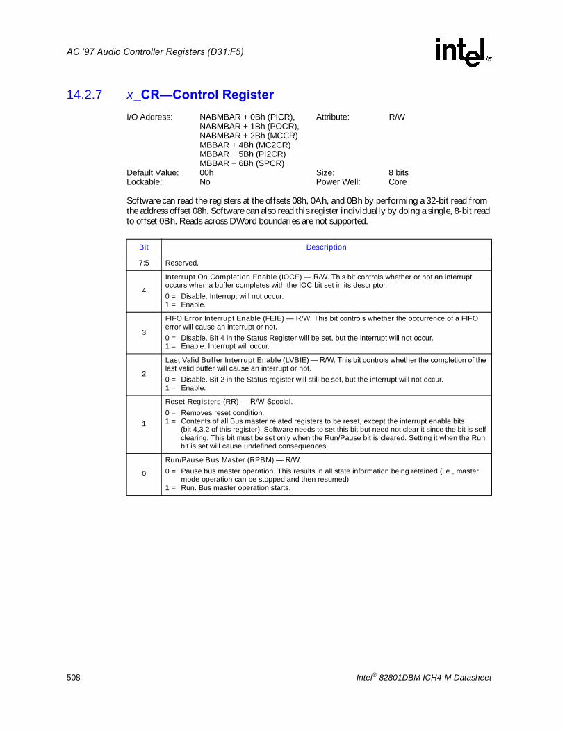
508 Intel® 82801DBM ICH4-M Datasheet
AC �97 Audio Controller Registers (D31:F5)
14.2.7 x_CR�Control RegisterI/O Address: NABMBAR + 0Bh (PICR), Attribute: R/W
NABMBAR + 1Bh (POCR), NABMBAR + 2Bh (MCCR)MBBAR + 4Bh (MC2CR)MBBAR + 5Bh (PI2CR)MBBAR + 6Bh (SPCR)
Default Value: 00h Size: 8 bitsLockable: No Power Well: Core
Software can read the registers at the offsets 08h, 0Ah, and 0Bh by performing a 32-bit read from the address offset 08h. Software can also read this register individually by doing a single, 8-bit read to offset 0Bh. Reads across DWord boundaries are not supported.
Bit Description
7:5 Reserved.
4
Interrupt On Completion Enable (IOCE) � R/W. This bit controls whether or not an interrupt occurs when a buffer completes with the IOC bit set in its descriptor.0 = Disable. Interrupt will not occur.1 = Enable.
3
FIFO Error Interrupt Enable (FEIE) � R/W. This bit controls whether the occurrence of a FIFO error will cause an interrupt or not.0 = Disable. Bit 4 in the Status Register will be set, but the interrupt will not occur.1 = Enable. Interrupt will occur.
2
Last Valid Buffer Interrupt Enable (LVBIE) � R/W. This bit controls whether the completion of the last valid buffer will cause an interrupt or not. 0 = Disable. Bit 2 in the Status register will still be set, but the interrupt will not occur.1 = Enable.
1
Reset Registers (RR) � R/W-Special. 0 = Removes reset condition.1 = Contents of all Bus master related registers to be reset, except the interrupt enable bits
(bit 4,3,2 of this register). Software needs to set this bit but need not clear it since the bit is self clearing. This bit must be set only when the Run/Pause bit is cleared. Setting it when the Run bit is set will cause undefined consequences.
0
Run/Pause Bus Master (RPBM) � R/W.0 = Pause bus master operation. This results in all state information being retained (i.e., master
mode operation can be stopped and then resumed).1 = Run. Bus master operation starts.
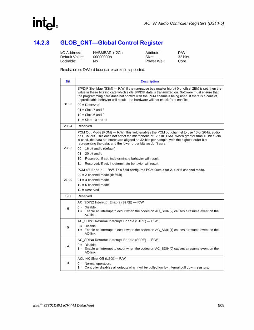
Intel® 82801DBM ICH4-M Datasheet 509
AC �97 Audio Controller Registers (D31:F5)
14.2.8 GLOB_CNT�Global Control RegisterI/O Address: NABMBAR + 2Ch Attribute: R/WDefault Value: 00000000h Size: 32 bitsLockable: No Power Well: Core
Reads across DWord boundaries are not supported.
Bit Description
31:30
S/PDIF Slot Map (SSM) � R/W. If the run/pause bus master bit (bit 0 of offset 2Bh) is set, then the value in these bits indicate which slots S/PDIF data is transmitted on. Software must ensure that the programming here does not conflict with the PCM channels being used. If there is a conflict, unpredictable behavior will result - the hardware will not check for a conflict.00 = Reserved01 = Slots 7 and 810 = Slots 6 and 911 = Slots 10 and 11
29:24 Reserved.
23:22
PCM Out Mode (POM) � R/W. This field enables the PCM out channel to use 16 or 20-bit audio on PCM out. This does not affect the microphone of S/PDIF DMA. When greater than 16 bit audio is used, the data structures are aligned as 32-bits per sample, with the highest order bits representing the data, and the lower order bits as don�t care.00 = 16 bit audio (default)01 = 20 bit audio10 = Reserved. If set, indeterminate behavior will result.11 = Reserved. If set, indeterminate behavior will result.
21:20
PCM 4/6 Enable � R/W. This field configures PCM Output for 2, 4 or 6 channel mode.00 = 2-channel mode (default)01 = 4-channel mode10 = 6-channel mode11 = Reserved
19:7 Reserved.
6
AC_SDIN2 Interrupt Enable (S2RE) � R/W. 0 = Disable.1 = Enable an interrupt to occur when the codec on AC_SDIN[2] causes a resume event on the
AC-link.
5
AC_SDIN1 Resume Interrupt Enable (S1RE) � R/W.0 = Disable.1 = Enable an interrupt to occur when the codec on AC_SDIN[1] causes a resume event on the
AC-link.
4
AC_SDIN0 Resume Interrupt Enable (S0RE) � R/W.0 = Disable.1 = Enable an interrupt to occur when the codec on AC_SDIN[0] causes a resume event on the
AC-link.
3ACLINK Shut Off (LSO) � R/W.0 = Normal operation.1 = Controller disables all outputs which will be pulled low by internal pull down resistors.

510 Intel® 82801DBM ICH4-M Datasheet
AC �97 Audio Controller Registers (D31:F5)
14.2.9 GLOB_STA�Global Status RegisterI/O Address: NABMBAR + 30h Attribute: RO, R/W, R/WCDefault Value: 00700000h Size: 32 bitsLockable: No Power Well: Core
Reads across DWord boundaries are not supported.
2
AC �97 Warm Reset � R/W-Special.0 = Normal operation.1 = Writing a 1 to this bit causes a warm reset to occur on the AC-link. The warm reset will awaken
a suspended codec without clearing its internal registers. If software attempts to perform a warm reset while bit_clk is running, the write will be ignored and the bit will not change. This bit is self-clearing (it remains set until the reset completes and bit_clk is seen on the ACLink, after which it clears itself).
1
AC �97 Cold Reset# � R/W.0 = Writing a 0 to this bit causes a cold reset to occur throughout the AC �97 circuitry. All data in
the controller and the codec will be lost. Software needs to clear this bit no sooner than the minimum number of ms have elapsed.
1 = This bit defaults to 0 and hence after reset, the driver needs to set this bit to a 1. The value of this bit is retained after suspends; hence, if this bit is set to a 1 prior to suspending, a cold reset is not generated automatically upon resuming.
NOTE: This bit is in the Core well.
0
GPI Interrupt Enable (GIE) � R/W. This bit controls whether the change in status of any GPI causes an interrupt. 0 = Bit 0 of the Global Status Register is set, but no interrupt is generated.1 = The change on value of a GPI causes an interrupt and sets bit 0 of the Global Status Register.
Bit Description
Bit Description
31:30 Reserved.
29
AC_SDIN2 Resume Interrupt (S2RI) � R/WC. This bit indicates that a resume event occurred on AC_SDIN[2]. This bit is not affected by D3HOT to D0 Reset.0 = Cleared by writing a 1 to this bit position.1 = Resume event occurred.
28
AC_SDIN2 Codec Ready (S2CR) � RO. This bit reflects the state of the codec ready bit in AC_SDIN[2]. Bus masters ignore the condition of the codec ready bits, so software must check this bit before starting the bus masters. Once the codec is �ready�, it must never go �not ready� spontaneously.0 = Not Ready.1 = Ready.
27Bit Clock Stopped (BCS) � RO. This bit indicates that the bit clock is not running. 0 = Transition is found on BIT_CLK.1 = ICH4 detects that there has been no transition on BIT_CLK for four consecutive PCI clocks.
26S/PDIF Interrupt (SPINT) � RO. 0 = When the specific status bit is cleared, this bit will be cleared.1 = Indicates that the S/PDIF out channel interrupt status bits have been set.
25PCM In 2 Interrupt (P2INT) � RO. 0 = When the specific status bit is cleared, this bit will be cleared.1 = Indicates that one of the PCM In 2 channel status bits have been set.

Intel® 82801DBM ICH4-M Datasheet 511
AC �97 Audio Controller Registers (D31:F5)
24Microphone 2 In Interrupt (M2INT) � RO. 0 = When the specific status bit is cleared, this bit will be cleared.1 = Indicates that one of the Mic in channel interrupts status bits has been set.
23:22
Sample Capabilities � RO. Indicates the capability to support more greater than 16-bit audio.00 = Reserved01 = 16 and 20-bit Audio supported (ICH4 value)10 = Reserved 11 = Reserved
21:20 Multichannel Capabilities � RO. Indicates the capability to support more 4 and 6 channels on PCM Out.
19:18 Reserved.
17
MD3 � R/W. This bit is a power down semaphore for Modem. The bit exists in the suspend well and maintains context across power states (except G3). The bit has no hardware function. It is used by software in conjunction with the AD3 bit to coordinate the entry of the two codecs into D3 state.This bit is not affected by D3HOT to D0 Reset.
16AD3 � R/W. This bit is a power down semaphore for Audio. The bit exists in the suspend well and maintains context across power states (except G3). The bit has no hardware function. It is used by software in conjunction with the MD3 bit to coordinate the entry of the two codecs into D3 state.This bit is not affected by D3HOT to D0 Reset.
15
Read Completion Status (RCS) � R/WC. This bit indicates the status of codec read completions.0 = A codec read completes normally.1 = A codec read results in a time-out. The bit remains set until being cleared by software writing a
1 to the bit location.This bit is not affected by D3HOT to D0 Reset.
14 Bit 3 of slot 12 � RO. Display bit 3 of the most recent slot 12.
13 Bit 2 of slot 12 � RO. Display bit 2 of the most recent slot 12.
12 Bit 1 of slot 12 � RO. Display bit 1 of the most recent slot 12.
11
AC_SDIN1 Resume Interrupt (S1RI) � R/WC. This bit indicates that a resume event occurred on AC_SDIN[1].0 = Cleared by writing a 1 to this bit position.1 = Resume event occurred.This bit is not affected by D3HOT to D0 Reset.
10
AC_SDIN0 Resume Interrupt (S0RI) � R/WC. This bit indicates that a resume event occurred on AC_SDIN[0].0 = Cleared by writing a 1 to this bit position.1 = Resume event occurred.This bit is not affected by D3HOT to D0 Reset.
9
AC_SDIN1 Codec Ready (S1CR) � RO. This bit reflects the state of the codec ready bit in AC_SDIN[1]. Bus masters ignore the condition of the codec ready bits, so software must check this bit before starting the bus masters. Once the codec is �ready�, it must never go �not ready� spontaneously.0 = Not Ready.1 = Ready.
8
AC_SDIN0 Codec Ready (S0CR) � RO. This bit reflects the state of the codec ready bit in AC_SDIN [0]. Bus masters ignore the condition of the codec ready bits, so software must check this bit before starting the bus masters. Once the codec is �ready�, it must never go �not ready� spontaneously.0 = Not Ready.1 = Ready.
Bit Description

512 Intel® 82801DBM ICH4-M Datasheet
AC �97 Audio Controller Registers (D31:F5)
14.2.10 CAS�Codec Access Semaphore RegisterI/O Address: NABMBAR + 34h Attribute: R/WDefault Value: 00h Size: 8 bitsLockable: No Power Well: Core
Reads across DWord boundaries are not supported.
7Mic In Interrupt (MINT) � RO. 0 = When the specific status bit is cleared, this bit will be cleared.1 = This bit indicates that one of the Mic in channel interrupts status bits has been set.
6PCM Out Interrupt (POINT) � RO. 0 = When the specific status bit is cleared, this bit will be cleared.1 = This bit indicates that one of the PCM out channel interrupts status bits has been set.
5PCM In Interrupt (PIINT) � RO. 0 = When the specific status bit is cleared, this bit will be cleared.1 = This bit indicates that one of the PCM in channel interrupts status bits has been set.
4:3 Reserved
2Modem Out Interrupt (MOINT) � RO. 0 = When the specific status bit is cleared, this bit will be cleared.1 = This bit indicates that one of the modem out channel interrupts status bits has been set.
1Modem In Interrupt (MIINT) � RO. 0 = When the specific status bit is cleared, this bit will be cleared.1 = This bit indicates that one of the modem in channel interrupts status bits has been set.
0
GPI Status Change Interrupt (GSCI) � R/WC. 0 = The bit is cleared by software writing a 1 to this bit location.1 = This bit reflects the state of bit 0 in slot 12, and is set when bit 0 of slot 12 is set. This indicates
that one of the GPIs changed state, and that the new values are available in slot 12. This bit is not affected by D3HOT to D0 Reset.
Bit Description
Bit Description
7:1 Reserved.
0
Codec Access Semaphore (CAS) � R/W-Special. This bit is read by software to check whether a codec access is currently in progress.0 = No access in progress.1 = The act of reading this register sets this bit to 1. The driver that read this bit can then perform
an I/O access. Once the access is completed, hardware automatically clears this bit.

Intel® 82801DBM ICH4-M Datasheet 513
AC �97 Audio Controller Registers (D31:F5)
14.2.11 SDM�SDATA_IN Map RegisterI/O Address: NABMBAR + 80h Attribute: R/W, RODefault Value: 00h Size: 8 bitsLockable: No Power Well: Core
Reads across DWord boundaries are not supported.
Bit Description
7:6
PCM In 2, Microphone In 2 Data In Line (DI2L) � R/W. When the SE bit is set, these bits indicate which AC_SDIN line should be used by the hardware for decoding the input slots for PCM In 2 and Microphone In 2. When the SE bit is cleared, the value of these bits are irrelevant, and PCM In 2 and Mic In 2 DMA engines are not available.00 = AC_SDIN001 = AC_SDIN110 = AC_SDIN211 = Reserved
5:4
PCM In 1, Microphone In 1 Data In Line (DI1L) � R/W. When the SE bit is set, these bits indicate which AC_SDIN line should be used by the hardware for decoding the input slots for PCM In 1 and Microphone In 1. When the SE bit is cleared, the value of these bits are irrelevant, and the PCM In 1 and Mic In 1 engines use the OR�d AC_SDIN lines.00 = AC_SDIN001 = AC_SDIN110 = AC_SDIN211 = Reserved
3Steer Enable (SE) � R/W. When set, the AC_SDIN lines are treated separately and not OR�d together before being sent to the DMA engines. When cleared, the AC_SDIN lines are OR�d together, and the �Microphone In 2� and �PCM In 2� DMA engines are not available.
2 Reserved � RO.
1:0
Last Codec Read Data Input (LDI) � RO. When a codec register is read, this indicates which AC_SDIN the read data returned on. Software can use this to determine how the codecs are mapped. The values are:00 = AC_SDIN001 = AC_SDIN110 = AC_SDIN211 = Reserved

514 Intel® 82801DBM ICH4-M Datasheet
AC �97 Audio Controller Registers (D31:F5)
This page is intentionally left blank.

Intel® 82801DBM ICH4-M Datasheet 515
AC �97 Modem Controller Registers (D31:F6)
15 AC �97 Modem Controller Registers (D31:F6)
15.1 AC �97 Modem PCI Configuration Space (D31:F6)Register address locations not shown in Table 15-1 should be treated as Reserved.
NOTE: Refer to the ICH4 Specification Update for the value of the Revision ID Register.
Note: Internal reset as a result of D3HOT to D0 transition will reset all the core well registers except the following BIOS programmed registers as BIOS may not be invoked following the D3-to-D0 transition. All resume well registers will not be reset by the D3HOT to D0 transition.
Core Well registers NOT reset by the D3HOT to D0 transition:
� offset 2Ch�2Dh; Subsystem Vendor ID (SVID)
� offset 2Eh�2Fh; Subsystem ID (SID)
Resume Well registers will not be reset by the D3HOT to D0 transition:
� offset 54h�55h; Power Management Control and Status (PCS)
Table 15-1. AC �97 Modem Controller PCI Configuration Register Address Map (Modem�D31:F6)
Offset Mnemonic Register Default Access
00�01h VID Vendor Identification 8086 RO02�03h DID Device Identification 24C6h RO
04�05h PCICMD PCI Command 0000 R/W, RO06�07h PCISTA PCI Device Status 0290h R/WC, RO
08h RID Revision Identification See Note RO09h PI Programming Interface 00 RO
0Ah SCC Sub Class Code 03h RO0Bh BCC Base Class Code 07h RO0Eh HEDT Header Type 00 RO
10�13h MMBAR Modem Mixer Base Address 00000001h R/W, RO
14�17h MBAR Modem Base Address 00000001h R/W, RO2C�2Dh SVID Subsystem Vendor ID 0000h R/WO2E�2Fh SID Subsystem ID 0000h R/WO
34h CAP_PTR Capabilities Pointer 50h RO
3Ch INTR_LN Interrupt Line 00h RO3Dh INT_PN Interrupt Pin 02h RO
50�51h PID PCI Power Management ID 0001h RO52�53h PC Power Management Capabilities C9C2h RO
54�55h PCS Power Management Control and Status 0000h R/WC, R/W
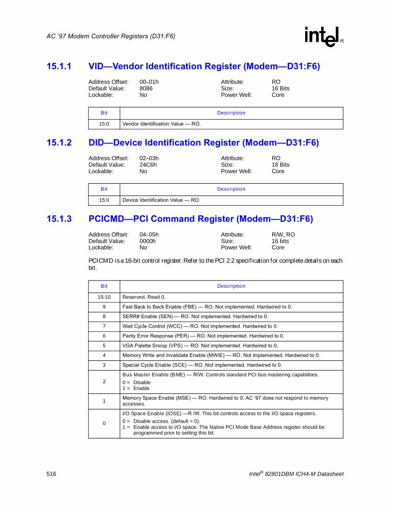
516 Intel® 82801DBM ICH4-M Datasheet
AC �97 Modem Controller Registers (D31:F6)
15.1.1 VID�Vendor Identification Register (Modem�D31:F6)Address Offset: 00�01h Attribute: RODefault Value: 8086 Size: 16 BitsLockable: No Power Well: Core
15.1.2 DID�Device Identification Register (Modem�D31:F6)Address Offset: 02�03h Attribute: RODefault Value: 24C6h Size: 16 BitsLockable: No Power Well: Core
15.1.3 PCICMD�PCI Command Register (Modem�D31:F6)Address Offset: 04�05h Attribute: R/W, RODefault Value: 0000h Size: 16 bitsLockable: No Power Well: Core
PCICMD is a 16-bit control register. Refer to the PCI 2.2 specification for complete details on each bit.
Bit Description
15:0 Vendor Identification Value � RO.
Bit Description
15:0 Device Identification Value � RO.
Bit Description
15:10 Reserved. Read 0.
9 Fast Back to Back Enable (FBE) � RO. Not implemented. Hardwired to 0.
8 SERR# Enable (SEN) � RO. Not implemented. Hardwired to 0.
7 Wait Cycle Control (WCC) � RO. Not implemented. Hardwired to 0.
6 Parity Error Response (PER) � RO. Not implemented. Hardwired to 0.
5 VGA Palette Snoop (VPS) � RO. Not implemented. Hardwired to 0.
4 Memory Write and Invalidate Enable (MWIE) � RO. Not implemented. Hardwired to 0.
3 Special Cycle Enable (SCE) � RO. Not implemented. Hardwired to 0.
2Bus Master Enable (BME) � R/W. Controls standard PCI bus mastering capabilities.0 = Disable1 = Enable
1 Memory Space Enable (MSE) � RO. Hardwired to 0; AC �97 does not respond to memory accesses.
0
I/O Space Enable (IOSE) �R /W. This bit controls access to the I/O space registers. 0 = Disable access. (default = 0).1 = Enable access to I/O space. The Native PCI Mode Base Address register should be
programmed prior to setting this bit.

Intel® 82801DBM ICH4-M Datasheet 517
AC �97 Modem Controller Registers (D31:F6)
15.1.4 PCISTA�Device Status Register (Modem�D31:F6)Address Offset: 06�07h Attribute: R/WC, RODefault Value: 0290h Size: 16 bitsLockable: No Power Well: Core
PCISTA is a 16-bit status register. Refer to the PCI 2.2 specification for complete details on each bit.
15.1.5 RID�Revision Identification Register (Modem�D31:F6)Address Offset: 08h Attribute: RODefault Value: See Bit Description Size: 8 BitsLockable: No Power Well: Core
15.1.6 PI�Programming Interface Register (Modem�D31:F6)Address Offset: 09h Attribute: RODefault Value: 00h Size: 8 bitsLockable: No Power Well: Core
Bit Description
15 Detected Parity Error (DPE) � RO. Not implemented. Hardwired to 0.
14 Signaled System Error (SSE) � RO. Not implemented. Hardwired to 0.
13Master Abort Status (MAS) � R/WC.0 = Software clears this bit by writing a 1 to the bit position.1 = Bus Master AC �97 interface function, as a master, generates a master abort.
12 Reserved. Read as 0.
11 Signaled Target Abort (STA) � RO. Not implemented. Hardwired to 0.
10:9DEVSEL# Timing Status (DEV_STS) � RO. This 2-bit field reflects the ICH4's DEVSEL# timing parameter. These read only bits indicate the ICH4's DEVSEL# timing when performing a positive decode.
8 Data Parity Error Detected (DPED) � RO. Not implemented. Hardwired to 0.
7 Fast Back to Back Capable (FB2BC) � RO. Hardwired to 1. This bit indicates that the ICH4 as a target is capable of fast back-to-back transactions.
6 User Definable Features (UDF) � RO. Not implemented. Hardwired to 0.
5 66 MHz Capable (66MHZ_CAP) � RO. Hardwired to 0.
4 Capabilities List (CAP_LIST) � RO. This field indicates that the controller contains a capabilities pointer list. The first item is pointed to by looking at configuration offset 34h.
3:0 Reserved
Bit Description
7:0 Revision Identification Value � RO. Refer to the ICH4 Specification Update for the value of the Revision ID Register.
Bit Description
7:0 Programming Interface � RO.

518 Intel® 82801DBM ICH4-M Datasheet
AC �97 Modem Controller Registers (D31:F6)
15.1.7 SCC�Sub Class Code Register (Modem�D31:F6)Address Offset: 0Ah Attribute: RODefault Value: 03h Size: 8 bitsLockable: No Power Well: Core
15.1.8 BCC�Base Class Code Register (Modem�D31:F6)Address Offset: 0Bh Attribute: RODefault Value: 07h Size: 8 bitsLockable: No Power Well: Core
15.1.9 HEDT�Header Type Register (Modem�D31:F6)Address Offset: 0Eh Attribute: RODefault Value: 00h Size: 8 bitsLockable: No Power Well: Core
Bit Description
7:0Sub Class Code � RO. 03h = Generic Modem.
Bit Description
7:0Base Class Code � RO. 07h = Simple Communications Controller.
Bit Description
7:0 Header Type � RO.
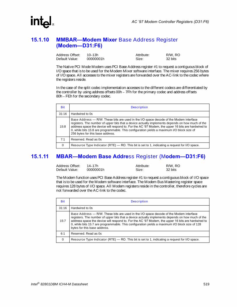
Intel® 82801DBM ICH4-M Datasheet 519
AC �97 Modem Controller Registers (D31:F6)
15.1.10 MMBAR�Modem Mixer Base Address Register (Modem�D31:F6)Address Offset: 10�13h Attribute: R/W, RODefault Value: 00000001h Size: 32 bits
The Native PCI Mode Modem uses PCI Base Address register #1 to request a contiguous block of I/O space that is to be used for the Modem Mixer software interface. The mixer requires 256 bytes of I/O space. All accesses to the mixer registers are forwarded over the AC-link to the codec where the registers reside.
In the case of the split codec implementation accesses to the different codecs are differentiated by the controller by using address offsets 00h � 7Fh for the primary codec and address offsets 80h � FEh for the secondary codec.
15.1.11 MBAR�Modem Base Address Register (Modem�D31:F6)Address Offset: 14�17h Attribute: R/W, RODefault Value: 00000001h Size: 32 bits
The Modem function uses PCI Base Address register #1 to request a contiguous block of I/O space that is to be used for the Modem software interface. The Modem Bus Mastering register space requires 128 bytes of I/O space. All Modem registers reside in the controller, therefore cycles are not forwarded over the AC-link to the codec.
Bit Description
31:16 Hardwired to 0s
15:8
Base Address � R/W. These bits are used in the I/O space decode of the Modem interface registers. The number of upper bits that a device actually implements depends on how much of the address space the device will respond to. For the AC �97 Modem, the upper 16 bits are hardwired to 0, while bits 15:8 are programmable. This configuration yields a maximum I/O block size of 256 bytes for this base address.
7:1 Reserved. Read as 0s
0 Resource Type Indicator (RTE) � RO. This bit is set to 1, indicating a request for I/O space.
Bit Description
31:16 Hardwired to 0s
15:7
Base Address � R/W. These bits are used in the I/O space decode of the Modem interface registers. The number of upper bits that a device actually implements depends on how much of the address space the device will respond to. For the AC �97 Modem, the upper 16 bits are hardwired to 0, while bits 15:7 are programmable. This configuration yields a maximum I/O block size of 128 bytes for this base address.
6:1 Reserved. Read as 0s
0 Resource Type Indicator (RTE) � RO. This bit is set to 1, indicating a request for I/O space.
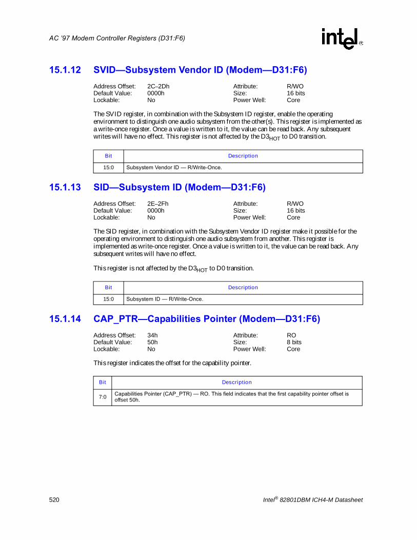
520 Intel® 82801DBM ICH4-M Datasheet
AC �97 Modem Controller Registers (D31:F6)
15.1.12 SVID�Subsystem Vendor ID (Modem�D31:F6)Address Offset: 2C�2Dh Attribute: R/WODefault Value: 0000h Size: 16 bitsLockable: No Power Well: Core
The SVID register, in combination with the Subsystem ID register, enable the operating environment to distinguish one audio subsystem from the other(s). This register is implemented as a write-once register. Once a value is written to it, the value can be read back. Any subsequent writes will have no effect. This register is not affected by the D3HOT to D0 transition.
15.1.13 SID�Subsystem ID (Modem�D31:F6)Address Offset: 2E�2Fh Attribute: R/WODefault Value: 0000h Size: 16 bitsLockable: No Power Well: Core
The SID register, in combination with the Subsystem Vendor ID register make it possible for the operating environment to distinguish one audio subsystem from another. This register is implemented as write-once register. Once a value is written to it, the value can be read back. Any subsequent writes will have no effect.
This register is not affected by the D3HOT to D0 transition.
15.1.14 CAP_PTR�Capabilities Pointer (Modem�D31:F6)Address Offset: 34h Attribute: RODefault Value: 50h Size: 8 bitsLockable: No Power Well: Core
This register indicates the offset for the capability pointer.
Bit Description
15:0 Subsystem Vendor ID � R/Write-Once.
Bit Description
15:0 Subsystem ID � R/Write-Once.
Bit Description
7:0 Capabilities Pointer (CAP_PTR) � RO. This field indicates that the first capability pointer offset is offset 50h.
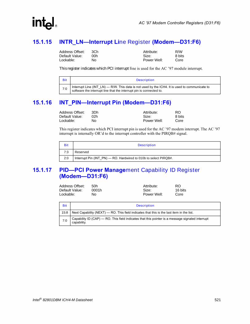
Intel® 82801DBM ICH4-M Datasheet 521
AC �97 Modem Controller Registers (D31:F6)
15.1.15 INTR_LN�Interrupt Line Register (Modem�D31:F6)Address Offset: 3Ch Attribute: R/WDefault Value: 00h Size: 8 bitsLockable: No Power Well: Core
This register indicates which PCI interrupt line is used for the AC �97 module interrupt.
15.1.16 INT_PIN�Interrupt Pin (Modem�D31:F6)Address Offset: 3Dh Attribute: RODefault Value: 02h Size: 8 bitsLockable: No Power Well: Core
This register indicates which PCI interrupt pin is used for the AC �97 modem interrupt. The AC �97 interrupt is internally OR�d to the interrupt controller with the PIRQB# signal.
15.1.17 PID�PCI Power Management Capability ID Register (Modem�D31:F6)Address Offset: 50h Attribute: RODefault Value: 0001h Size: 16 bitsLockable: No Power Well: Core
Bit Description
7:0 Interrupt Line (INT_LN) � R/W. This data is not used by the ICH4. It is used to communicate to software the interrupt line that the interrupt pin is connected to.
Bit Description
7:3 Reserved
2:0 Interrupt Pin (INT_PN) � RO. Hardwired to 010b to select PIRQB#.
Bit Description
15:8 Next Capability (NEXT) � RO. This field indicates that this is the last item in the list.
7:0 Capability ID (CAP) � RO. This field indicates that this pointer is a message signaled interrupt capability.

522 Intel® 82801DBM ICH4-M Datasheet
AC �97 Modem Controller Registers (D31:F6)
15.1.18 PC�Power Management Capabilities Register (Modem�D31:F6)Address Offset: 52h Attribute: RODefault Value: C9C2h Size: 16 bitsLockable: No Power Well: Core
15.1.19 PCS�Power Management Control and Status Register (Modem�D31:F6)Address Offset: 54h Attribute: R/W, R/WCDefault Value: 0000h Size: 16 bitsLockable: No Power Well: Resume
This register is not affected by the D3HOT to D0 transition.
Bit Description
15:11 PME Support � RO. This field indicates PME# can be generated from all D states.
10:9 Reserved.
8:6 Auxiliary Current � RO. This field reports 375 mA maximum Suspend well current required when in the D3cold state.
5 Device Specific Initialization (DSI) � RO. This bit indicates that no device-specific initialization is required.
4 Reserved � RO.
3 PME Clock � RO. This bit indicates that PCI clock is not required to generate PME#.
2:0 Version � RO. This field indicates support for Revision 1.1 of the PCI Power Management Specification.
Bit Description
15
PME Status (PMES) � RW/C. 0 = Software clears this bit by writing a 1 to the bit position.1 = This bit is set when the AC �97 controller would normally assert the PME# signal independent of
the state of the PME_En bit. This bit resides in the resume well.
14:9 Reserved � RO.
8 PME Enable (PMEE) � R/W. When set, and if corresponding PMES is also set, the AC'97 controller sets the AC97_STS bit in the GPE0_STS register
7:2 Reserved � RO.
1:0
Power State � R/W. This field is used both to determine the current power state of the AC �97 controller and to set a new power state. The values are:00 = D0 state01 = not supported10 = not supported11 = D3HOT stateWhen in the D3HOT state, the AC �97 controller�s configuration space is available, but the I/O and memory spaces are not. Additionally, interrupts are blocked.If software attempts to write a value of 10b or 01b in to this field, the write operation must complete normally; however, the data is discarded and no state change occurs.

Intel® 82801DBM ICH4-M Datasheet 523
AC �97 Modem Controller Registers (D31:F6)
15.2 AC �97 Modem I/O Space (D31:F6)In the case of the split codec implementation, accesses to the modem mixer registers in different codecs are differentiated by the controller by using address offsets 00h � 7Fh for the primary codec and address offsets 80h � FEh for the secondary codec. Table 15-2 shows the register addresses for the modem mixer registers.
NOTES:1. Registers in italics are for functions not supported by the ICH4.2. Software should not try to access reserved registers.3. The ICH4 supports a modem codec connected to AC_SDIN[2:0], as long as the Codec ID is 00 or 01.
However, the ICH4 does not support more than one modem codec. For a complete list of topologies, see the appropriate chipset Platform Design Guide.
The Global Control (GLOB_CNT) and Global Status (GLOB_STA) registers are aliased to the same global registers in the audio and modem I/O space. Therefore, a read/write to these registers in either audio or modem I/O space affects the same physical register. S/W could access these registers as bytes, word, or DWord quantities, but reads must not cross DWord boundaries.
These registers exist in I/O space and reside in the AC �97 controller. The two channels, Modem in and Modem out, each have their own set of Bus Mastering registers. The following register descriptions apply to both channels. The naming prefix convention used is as follows:
MI = Modem in channelMO = Modem out channel
Table 15-2. Intel® ICH4 Modem Mixer Register Configuration
RegisterMMBAR Exposed Registers (D31:F6)
Pri. Sec.
00h:38h 80h:B8h Intel RESERVED
3Ch BCh Extended Modem ID
3Eh BEh Extended Modem Stat/Ctrl
40h C0h Line 1 DAC/ADC Rate
42h C2h Line 2 DAC/ADC Rate
44h C4h Handset DAC/ADC Rate
46h C6h Line 1 DAC/ADC Level Mute
48h C8h Line 2 DAC/ADC Level Mute
4Ah CAh Handset DAC/ADC Level Mute
4Ch CCh GPIO Pin Config
4Eh CEh GPIO Polarity/Type
50h D0h GPIO Pin Sticky
52h D2h GPIO Pin Wake Up
54h D4h GPIO Pin Status
56h D6h Misc. Modem AFE Stat/Ctrl
58h D8h AC �97 Reserved
5Ah DAh Vendor Reserved
7Ch FCh Vendor ID1
7Eh FEh Vendor ID2
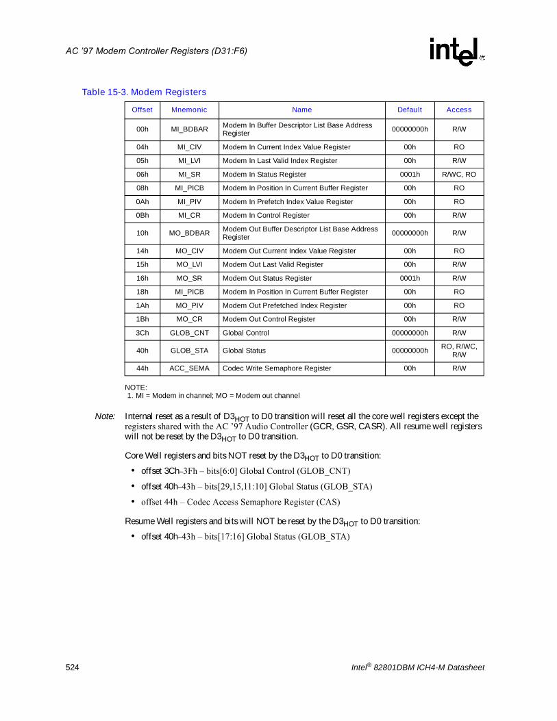
524 Intel® 82801DBM ICH4-M Datasheet
AC �97 Modem Controller Registers (D31:F6)
NOTE:1. MI = Modem in channel; MO = Modem out channel
Note: Internal reset as a result of D3HOT to D0 transition will reset all the core well registers except the registers shared with the AC �97 Audio Controller (GCR, GSR, CASR). All resume well registers will not be reset by the D3HOT to D0 transition.
Core Well registers and bits NOT reset by the D3HOT to D0 transition:
� offset 3Ch�3Fh � bits[6:0] Global Control (GLOB_CNT)
� offset 40h�43h � bits[29,15,11:10] Global Status (GLOB_STA)
� offset 44h � Codec Access Semaphore Register (CAS)
Resume Well registers and bits will NOT be reset by the D3HOT to D0 transition:
� offset 40h�43h � bits[17:16] Global Status (GLOB_STA)
Table 15-3. Modem Registers
Offset Mnemonic Name Default Access
00h MI_BDBAR Modem In Buffer Descriptor List Base Address Register 00000000h R/W
04h MI_CIV Modem In Current Index Value Register 00h RO
05h MI_LVI Modem In Last Valid Index Register 00h R/W
06h MI_SR Modem In Status Register 0001h R/WC, RO
08h MI_PICB Modem In Position In Current Buffer Register 00h RO
0Ah MI_PIV Modem In Prefetch Index Value Register 00h RO
0Bh MI_CR Modem In Control Register 00h R/W
10h MO_BDBAR Modem Out Buffer Descriptor List Base Address Register 00000000h R/W
14h MO_CIV Modem Out Current Index Value Register 00h RO
15h MO_LVI Modem Out Last Valid Register 00h R/W
16h MO_SR Modem Out Status Register 0001h R/W
18h MI_PICB Modem In Position In Current Buffer Register 00h RO
1Ah MO_PIV Modem Out Prefetched Index Register 00h RO
1Bh MO_CR Modem Out Control Register 00h R/W
3Ch GLOB_CNT Global Control 00000000h R/W
40h GLOB_STA Global Status 00000000h RO, R/WC,R/W
44h ACC_SEMA Codec Write Semaphore Register 00h R/W

Intel® 82801DBM ICH4-M Datasheet 525
AC �97 Modem Controller Registers (D31:F6)
15.2.1 x_BDBAR�Buffer Descriptor List Base Address Register I/O Address: MBAR + 00h (MIBDBAR), Attribute: R/W
MBAR + 10h (MOBDBAR)Default Value: 00000000h Size: 32 bitsLockable: No Power Well: Core
Software can read the register at offset 00h by performing a single 32-bit read from address offset 00h. Reads across DWord boundaries are not supported.
15.2.2 x_CIV�Current Index Value Register I/O Address: MBAR + 04h (MICIV), Attribute: RO
MBAR + 14h (MOCIV),Default Value: 00h Size: 8 bitsLockable: No Power Well: Core
Software can read the registers at offsets 04h, 05h and 06h simultaneously by performing a single, 32-bit read from address offset 04h. Software can also read this register individually by doing a single, 8-bit read to offset 04h. Reads across DWord boundaries are not supported.
15.2.3 x_LVI�Last Valid Index RegisterI/O Address: MBAR + 05h (MILVI), Attribute: R/W
MBAR + 15h (MOLVI)Default Value: 00h Power Well: Core
Software can read the registers at offsets 04h, 05h and 06h simultaneously by performing a single, 32-bit read from address offset 04h. Software can also read this register individually by doing a single, 8-bit read to offset 05h. Reads across DWord boundaries are not supported.
Bit Description
31:3 Buffer Descriptor List Base Address [31:3] � R/W. These bits represent address bits 31:3. The entries should be aligned on 8-byte boundaries.
2:0 Hardwired to 0.
Bit Description
7:5 Hardwired to 0.
4:0Current Index Value [4:0] � RO. These bits represent which buffer descriptor within the list of 16 descriptors is being processed currently. As each descriptor is processed, this value is incremented.
Bit Description
7:5 Hardwired to 0
4:0 Last Valid Index [4:0] � R/W. These bits indicate the last valid descriptor in the list. This value is updated by the software as it prepares new buffers and adds to the list.

526 Intel® 82801DBM ICH4-M Datasheet
AC �97 Modem Controller Registers (D31:F6)
15.2.4 x_SR�Status RegisterI/O Address: MBAR + 06h (MISR), Attribute: R/WC, RO
MBAR + 16h (MOSR)Default Value: 0001h Size: 16 bitsLockable: No Power Well: Core
Software can read the registers at offsets 04h, 05h and 06h simultaneously by performing a single, 32-bit read from address offset 04h. Software can also read this register individually by doing a single, 16-bit read to offset 06h. Reads across DWord boundaries are not supported.
Bit Description
15:5 Reserved
4
FIFO Error (FIFOE) � R/WC.0 = Cleared by writing a 1 to this bit position.1 = FIFO error occurs.
�Modem in: FIFO error indicates a FIFO overrun. The FIFO pointers don't increment, the incoming data is not written into the FIFO, thereby being lost.
�Modem out: FIFO error indicates a FIFO underrun. The sample transmitted in this case should be the last valid sample.
The ICH4 will set the FIFOE bit if the under-run or overrun occurs when there are more valid buffers to process.
3
Buffer Completion Interrupt Status (BCIS) � R/WC.0 = Cleared by writing a 1 to this bit position.1 = Set by the hardware after the last sample of a buffer has been processed, AND if the Interrupt
on Completion (IOC) bit is set in the command byte of the buffer descriptor. Remains active until software clears bit.
2
Last Valid Buffer Completion Interrupt (LVBCI) � R/WC. 0 = Cleared by writing a 1 to this bit position1 = Set by hardware when last valid buffer has been processed. It remains active until cleared by
software. This bit indicates the occurrence of the event signified by the last valid buffer being processed. Thus, this is an event status bit that can be cleared by software once this event has been recognized. This event will cause an interrupt if the enable bit in the Control Register is set. The interrupt is cleared when the software clears this bit.
In the case of transmits (PCM out, Modem out) this bit is set, after the last valid buffer has been fetched (not after transmitting it). While in the case of Receives, this bit is set after the data for the last buffer has been written to memory.
1
Current Equals Last Valid (CELV) � RO. 0 = Hardware clears when controller exists state (i.e., until a new value is written to the LVI
register). 1 = Current Index is equal to the value in the Last Valid Index Register, AND the buffer pointed to
by the CIV has been processed (i.e., after the last valid buffer has been processed). This bit is very similar to bit 2, except, this bit reflects the state rather than the event. This bit reflects the state of the controller, and remains set until the controller exits this state.
0
DMA Controller Halted (DCH)� RO.0 = Running.1 = Halted. This could happen because of the Start/Stop bit being cleared and the DMA engines
are idle, or it could happen once the controller has processed the last valid buffer.

Intel® 82801DBM ICH4-M Datasheet 527
AC �97 Modem Controller Registers (D31:F6)
15.2.5 x_PICB�Position in Current Buffer RegisterI/O Address: MBAR + 08h (MIPICB), Attribute: RO
MBAR + 18h (MOPICB),Default Value: 0000h Size: 16 bitsLockable: No Power Well: Core
Software can read the registers at the offsets 08h, 0Ah, and 0Bh by performing a 32-bit read from the address offset 08h. Software can also read this register individually by doing a single, 16-bit read to offset 08h. Reads across DWord boundaries are not supported.
15.2.6 x_PIV�Prefetch Index Value RegisterI/O Address: MBAR + 0Ah (MIPIV), Attribute: RO
MBAR + 1Ah (MOPIV)Default Value: 00h Size: 8 bitsLockable: No Power Well: Core
Software can read the registers at the offsets 08h, 0Ah, and 0Bh by performing a 32-bit read from the address offset 08h. Software can also read this register individually by doing a single, 8-bit read to offset 0Ah. Reads across DWord boundaries are not supported.
Bit Description
15:0 Position In Current Buffer [15:0] � RO. These bits represent the number of samples left to be processed in the current buffer.
Bit Description
7:5 Hardwired to 0
4:0 Prefetched Index Value [4:0] � RO. These bits represent which buffer descriptor in the list has been prefetched.
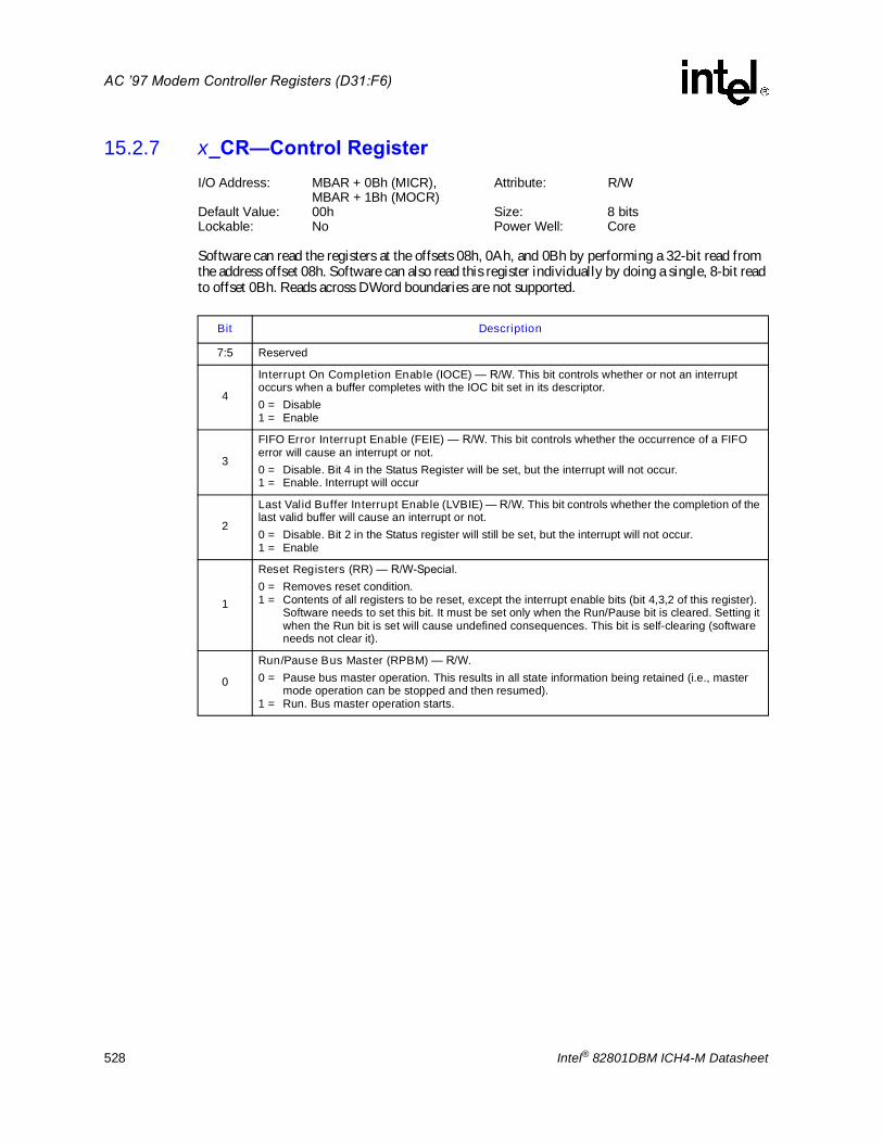
528 Intel® 82801DBM ICH4-M Datasheet
AC �97 Modem Controller Registers (D31:F6)
15.2.7 x_CR�Control RegisterI/O Address: MBAR + 0Bh (MICR), Attribute: R/W
MBAR + 1Bh (MOCR)Default Value: 00h Size: 8 bitsLockable: No Power Well: Core
Software can read the registers at the offsets 08h, 0Ah, and 0Bh by performing a 32-bit read from the address offset 08h. Software can also read this register individually by doing a single, 8-bit read to offset 0Bh. Reads across DWord boundaries are not supported.
Bit Description
7:5 Reserved
4
Interrupt On Completion Enable (IOCE) � R/W. This bit controls whether or not an interrupt occurs when a buffer completes with the IOC bit set in its descriptor.0 = Disable1 = Enable
3
FIFO Error Interrupt Enable (FEIE) � R/W. This bit controls whether the occurrence of a FIFO error will cause an interrupt or not.0 = Disable. Bit 4 in the Status Register will be set, but the interrupt will not occur.1 = Enable. Interrupt will occur
2
Last Valid Buffer Interrupt Enable (LVBIE) � R/W. This bit controls whether the completion of the last valid buffer will cause an interrupt or not. 0 = Disable. Bit 2 in the Status register will still be set, but the interrupt will not occur.1 = Enable
1
Reset Registers (RR) � R/W-Special. 0 = Removes reset condition.1 = Contents of all registers to be reset, except the interrupt enable bits (bit 4,3,2 of this register).
Software needs to set this bit. It must be set only when the Run/Pause bit is cleared. Setting it when the Run bit is set will cause undefined consequences. This bit is self-clearing (software needs not clear it).
0
Run/Pause Bus Master (RPBM) � R/W. 0 = Pause bus master operation. This results in all state information being retained (i.e., master
mode operation can be stopped and then resumed).1 = Run. Bus master operation starts.

Intel® 82801DBM ICH4-M Datasheet 529
AC �97 Modem Controller Registers (D31:F6)
15.2.8 GLOB_CNT�Global Control RegisterI/O Address: MBAR + 3Ch Attribute: R/WDefault Value: 00000000h Size: 32 bitsLockable: No Power Well: Core
Reads across DWord boundaries are not supported.
Bit Description
31:7 Reserved.
6
AC_SDIN2 Interrupt Enable (S2RE) � R/W. 0 = Disable.1 = Enable an interrupt to occur when the codec on AC_SDIN[2] causes a resume event on the
AC-link.
5
AC_SDIN1 Resume Interrupt Enable (S1RE) � R/W.0 = Disable.1 = Enable an interrupt to occur when the codec on AC_SDIN[1] causes a resume event on the
AC-link.
4
AC_SDIN0 Resume Interrupt Enable (S0RE) � R/W.0 = Disable.1 = Enable an interrupt to occur when the codec on AC_SDIN[0] causes a resume event on the
AC-link.
3ACLINK Shut Off (LSO) � R/W.0 = Normal operation.1 = Controller disables all outputs which will be pulled low by internal pull down resistors.
2
AC �97 Warm Reset � R/W-Special.0 = Normal operation.1 = Writing a 1 to this bit causes a warm reset to occur on the AC-link. The warm reset will awaken
a suspended codec without clearing its internal registers. If software attempts to perform a warm reset while bit_clk is running, the write will be ignored and the bit will not change. This bit is self-clearing (it remains set until the reset completes and bit_clk is seen on the ACLink, after which it clears itself).
1
AC �97 Cold Reset# � R/W.0 = Writing a 0 to this bit causes a cold reset to occur throughout the AC �97 circuitry. All data in
the controller and the codec will be lost. Software needs to clear this bit no sooner than the minimum number of ms have elapsed.
1 = This bit defaults to 0 and hence after reset, the driver needs to set this bit to a 1. The value of this bit is retained after suspends; hence, if this bit is set to a 1 prior to suspending, a cold reset is not generated automatically upon resuming.
NOTE: This bit is in the Core well.
0
GPI Interrupt Enable (GIE) � R/W. This bit controls whether the change in status of any GPI causes an interrupt. 0 = Bit 0 of the Global Status Register is set, but no interrupt is generated.1 = The change on value of a GPI causes an interrupt and sets bit 0 of the Global Status Register.

530 Intel® 82801DBM ICH4-M Datasheet
AC �97 Modem Controller Registers (D31:F6)
15.2.9 GLOB_STA�Global Status RegisterI/O Address: MBAR + 40h Attribute: RO, R/W, R/WCDefault Value: 00300000h Size: 32 bitsLockable: No Power Well: Core
On reads from a codec, the controller will give the codec a maximum of 4 frames to respond, after which if no response is received, it will return a dummy read completion to the processor (with all F�s on the data) and also set the Read Completion Status bit in the Global Status Register.
Reads across DWord boundaries are not supported.
Bit Description
31:30 Reserved.
29
AC_SDIN2 Resume Interrupt (S2RI) � R/WC. This bit indicates that a resume event occurred on AC_SDIN[2].0 = Cleared by writing a 1 to this bit position.1 = Resume event occurred.This bit is not affected by D3HOT to D0 Reset.
28
AC_SDIN2 Codec Ready (S2CR) � RO. Reflects the state of the codec ready bit in AC_SDIN[2]. Bus masters ignore the condition of the codec ready bits, so software must check this bit before starting the bus masters. Once the codec is �ready�, it must never go �not ready� spontaneously.0 = Not Ready.1 = Ready.
27
Bit Clock Stopped (BCS) � RO. Indicates that the bit clock is not running. 0 = Running. It is cleared if a transition is found on BIT_CLK.1 = Stopped. This bit is set if the ICH4 detects that there has been no transition on BIT_CLK for
four consecutive PCI clocks.
26S/PDIF Interrupt (SPINT) � RO. 0 = When the specific status bit is cleared, this bit will be cleared.1 = Indicates that the S/PDIF out channel interrupt status bits have been set.
25PCM In 2 Interrupt (P2INT) � RO. 0 = When the specific status bit is cleared, this bit will be cleared.1 = Indicates that one of the PCM In 2 channel status bits have been set.
24Microphone 2 In Interrupt (M2INT) � RO. 0 = When the specific status bit is cleared, this bit will be cleared.1 = Indicates that one of the Mic in channel interrupts status bits has been set.
23:22
Sample Capabilities � RO. Indicates the capability to support more greater than 16-bit audio.00 = Reserved01 = 16 and 20-bit Audio supported (ICH4 value)10 = Reserved 11 = Reserved
21:20 Multichannel Capabilities � RO. Indicates the capability to support more 4 and 6 channels on PCM Out.
19:18 Reserved.
17
MD3 � R/W. Power down semaphore for Modem. This bit exists in the suspend well and maintains context across power states (except G3). The bit has no hardware function. It is used by software in conjunction with the AD3 bit to coordinate the entry of the two codecs into D3 state.This bit is not affected by D3HOT to D0 Reset.
16AD3 � R/W. Power down semaphore for Audio. This bit exists in the suspend well and maintains context across power states (except G3). The bit has no hardware function. It is used by software in conjunction with the MD3 bit to coordinate the entry of the two codecs into D3 state.This bit is not affected by D3HOT to D0 Reset.

Intel® 82801DBM ICH4-M Datasheet 531
AC �97 Modem Controller Registers (D31:F6)
15
Read Completion Status (RCS) � R/WC. This bit indicates the status of codec read completions.0 = A codec read completes normally.1 = A codec read results in a time-out. The bit remains set until being cleared by software writing a
1 to the bit location.This bit is not affected by D3HOT to D0 Reset.
14 Bit 3 of slot 12 � RO. Display bit 3 of the most recent slot 12.13 Bit 2 of slot 12 � RO. Display bit 2 of the most recent slot 12.12 Bit 1 of slot 12 � RO. Display bit 1 of the most recent slot 12.
11
AC_SDIN1 Resume Interrupt (S1RI) � R/WC. This bit indicates that a resume event occurred on AC_SDIN[1].0 = Cleared by writing a 1 to this bit position.1 = Resume event occurred.This bit is not affected by D3HOT to D0 Reset.
10
AC_SDIN0 Resume Interrupt (S0RI) � R/WC. This bit indicates that a resume event occurred on AC_SDIN[0].0 = Cleared by writing a 1 to this bit position.1 = Resume event occurred.This bit is not affected by D3HOT to D0 Reset.
9
AC_SDIN1 Codec Ready (S1CR) � RO. Reflects the state of the codec ready bit in AC_SDIN[1]. Bus masters ignore the condition of the codec ready bits, so software must check this bit before starting the bus masters. Once the codec is �ready�, it must never go �not ready� spontaneously.0 = Not Ready.1 = Ready.
8
AC_SDIN0 Codec Ready (S0CR) � RO. Reflects the state of the codec ready bit in AC_SDIN [0]. Bus masters ignore the condition of the codec ready bits, so software must check this bit before starting the bus masters. Once the codec is �ready�, it must never go �not ready� spontaneously.0 = Not Ready.1 = Ready.
7Mic In Interrupt (MINT) � RO. 0 = When the specific status bit is cleared, this bit will be cleared.1 = This bit indicates that one of the Mic in channel interrupts status bits has been set.
6PCM Out Interrupt (POINT) � RO. 0 = When the specific status bit is cleared, this bit will be cleared.1 = This bit indicates that one of the PCM out channel interrupts status bits has been set.
5PCM In Interrupt (PIINT) � RO. 0 = When the specific status bit is cleared, this bit will be cleared.1 = This bit indicates that one of the PCM in channel interrupts status bits has been set.
4:3 Reserved
2Modem Out Interrupt (MOINT) � RO. 0 = When the specific status bit is cleared, this bit will be cleared.1 = This bit indicates that one of the modem out channel interrupts status bits has been set.
1Modem In Interrupt (MIINT) � RO. 0 = When the specific status bit is cleared, this bit will be cleared.1 = This bit indicates that one of the modem in channel interrupts status bits has been set.
0
GPI Status Change Interrupt (GSCI) � RWC. 0 = The bit is cleared by software writing a 1 to this bit location.1 = This bit reflects the state of bit 0 in slot 12, and is set when bit 0 of slot 12 is set. This indicates
that one of the GPIs changed state, and that the new values are available in slot 12. This bit is not affected by D3HOT to D0 Reset.
Bit Description

532 Intel® 82801DBM ICH4-M Datasheet
AC �97 Modem Controller Registers (D31:F6)
15.2.10 CAS�Codec Access Semaphore RegisterI/O Address: NABMBAR + 44h Attribute: R/WDefault Value: 00h Size: 8 bitsLockable: No Power Well: Core
Reads across DWord boundaries are not supported.
Bit Description
7:1 Reserved
0
Codec Access Semaphore (CAS) � R/W-Special. This bit is read by software to check whether a codec access is currently in progress.0 = No access in progress.1 = The act of reading this register sets this bit to 1. The driver that read this bit can then perform
an I/O access. Once the access is completed, hardware automatically clears this bit.

Intel® 82801DBM ICH4-M Datasheet 533
Ballout Definition
16 Ballout Definition
This section contains the ICH4 ballout information. Figure 16-1 and Figure 16-2 provide a graphical illustration of how the ballout maps to the 421 BGA package. Table 16-1 provides the BGA ball list, sorted alphabetically by signal name.

534 Intel® 82801DBM ICH4-M Datasheet
Ballout Definition
Figure 16-1. Intel® ICH4 Ballout (Topview�Left Side)
1 2 3 4 5 6 7 8 9 10 11 12
A Vss REQ1# PIRQD# Vss Vcc3_3 REQB#/ REQ5#/ GPIO1
GNT2# EE_DOUT LAN_RXD1 LAN_RXD0 LAN_RXD2 LAN_TXD2
B REQ0# Vcc3_3 REQ2# PIRQC# REQA# / GPIO0 REQ4# GNT3# AC_BIT_CLK Vss LAN_TXD0 LAN_RSTSYNC Vss
C GNT0# PIRQB# PIRQG# / GPIO4
PIRQH# / GPIO5
GNTB#/ GNT5#/ GPIO17
Vss REQ3# PIRQE# / GPIO2
AC_SYNC LAN_TXD1 LAN_CLK EE_SHCLK
D Vss AD30 AD28 Vss PIRQA# GNT4# PIRQF# / GPIO3
Vss AC_SDOUT EE_CS EE_DIN Vss
E AD26 AD24 AD20 AD22 AD18 GNT1# V5REF GNTA# / GPIO16
VccLAN3_3 Vss VccSus3_3 VccSus1_5
F FRAME# TRDY# STOP# AD16 AD15 VccLAN1_5 VccLAN1_5 Vss VccLAN3_3 VccSus3_3
G PAR AD9 Vss AD11 AD4 Vss
H Vss AD13 AD2 AD6 AD0 Vcc3_3
J Vcc3_3 C/BE0# AD1 AD5 AD7 Vss
K AD3 AD8 Vss C/BE1# SERR# Vcc3_3 Vcc1_5 Vss Vcc1_5
L AD10 AD12 AD14 PERR# IRDY# Vss Vss Vss
M Vss PLOCK# DEVSEL# C/BE2# AD23 Vcc3_3 Vss Vss
N AD17 AD19 AD21 C/BE3# Vss Vss Vss Vss
P AD25 AD27 Vss AD31 PCICLK Vcc3_3 Vcc1_5 Vss Vcc3_3
R AD29 AGPBUSY# GPIO7 LAD1 / FWH1 Vss VccSus1_5
T Vss LAD0 / FWH0 C3_STAT# LAD2 / FWH2 LFRAME# / FWH4
VccSus1_5
U Vcc3_3 LAD3 / FWH3 LDRQ0# LDRQ1# PCIRST# VccSus1_5
V THRM# GPIO25 Vss GPIO8 GPIO12 V5REF VccSus3_3 VccSus3_3 VccSus3_3 Vcc3_3
W GPIO27 PME# GPIO13 GPIO28 Vss INTRUDER# RTCRST# Vss PDD11 PDD13 PDD14 PDIOW#
Y RI# SLP_S4# SYS_RESET# SLP_S3# LAN_RST# VBIAS Vss PDD6 PDD9 PDD2 PDD15 PDDACK#
AA PWRBTN# SLP_S5# Vss SUSCLK SMBALERT# / GPIO11
RSMRST# PDD4 PDD7 Vss PDD3 PDDREQ Vss
AB SMLINK1 BATLOW# SUS_STAT# / LPCPD#
SMBDATA VccRTC PWROK Vss PDD5 PDD8 PDD12 PDD0 PIORDY
AC Vss CLKRUN# SMLINK0 SMBCLK Vss RTCX2 RTCX1 Vcc3_3 PDD10 Vss PDD1 PDIOR#
1 2 3 4 5 6 7 8 9 10 11 12

Intel® 82801DBM ICH4-M Datasheet 535
Ballout Definition
Figure 16-2. Intel® ICH4 Ballout (Topview�Right Side)
13 14 15 16 17 18 19 20 21 22 23
AC_SDIN1 OC4# OC2# Vss USBP5P Vss USBP3P Vss USBP1P Vss USBRBIAS A
AC_SDIN2 OC3# OC0# Vss USBP5N Vss USBP3N Vss USBP1N Vss USBRBIAS# B
AC_RST# OC1# Vss USBP4P Vss USBP2P Vss USBP0P Vss VccPLL Vss C
AC_SDIN0 OC5# Vss USBP4N Vss USBP2N Vss USBP0N Vss Vss Vss D
VccSus1_5 Vss V5REF_Sus Vss Vss Vss Vss VccSus1_5 Vss Vss GPIO43 E
VccSus1_5 VccSus3_3 VccSus3_3 VccSus3_3 VccSus3_3 CLK48 GPIO34 GPIO36 GPIO42 GPIO38 F
VccSus1_5 Vss GPIO35 Vss GPIO33 GPIO40 G
Vcc3_3 APICD0 GPIO37 GPIO41 GPIO39 SPKR H
Vcc3_3 APICCLK GPIO32 SSMUXSEL SERIRQ CLK14 J
Vss VccSus3_3 Vcc1_5 Vss APICD1 HI11 Vcc1_5 Vss K
Vss Vss HI0 HI1 Vss HI9 VccHI L
Vss VccHI HI2 Vss HI3 Vss HIREF M
Vss Vss Vss HI_STB# / HI_STBF
Vss HI10 Vss N
Vss V_CPU_IO VccHI HI4 Vss HI_STB /
HI_STBS
Vss HI8 P
Vss HI5 HI7 Vss HI_VSWING HICOMP R
Vcc1_5 Vss HI6 CLK66 VccHI Vss T
V_CPU_IO Vcc1_5 Vss CPUSLP# RCIN# DPSLP# U
Vcc1_5 Vss Vcc3_3 Vss Vcc3_3 VGATE /
VRMPWRGD
DPRSLPVR NMI INIT# STPCLK# V
PDA2 SDD6 SDD4 SDD2 SDD0 SLP_S1# STP_CPU# THRMTRIP# IGNNE# Vss SMI# W
PDCS1# SDD8 SDD11 SDD13 SDD15 SDIOR# Vss CPUPERF# STP_PCI# A20GATE CPUPWRGD Y
PDA0 SDD7 SDD10 Vss SDD14 SDIOW# IRQ15 SDA0 FERR# Vss V_CPU_IO AA
PDA1 PDCS3# SDD5 SDD12 SDD1 SDDREQ SDDACK# Vss SDCS1# INTR A20M# AB
IRQ14 Vss SDD9 SDD3 Vcc3_3 Vss SIORDY SDA1 SDA2 SDCS3# Vss AC
13 14 15 16 17 18 19 20 21 22 23

Ballout Definition
536 Intel® 82801DBM ICH4-M Datasheet
Table 16-1. Intel® ICH4 Ball List
Signal Name Ball #
A20GATE Y22
A20M# AB23
AC_BIT_CLK B8
AC_RST# C13
AC_SDIN0 D13
AC_SDIN1 A13
AC_SDIN2 B13
AC_SDOUT D9
AC_SYNC C9
AD0 H5
AD1 J3
AD2 H3
AD3 K1
AD4 G5
AD5 J4
AD6 H4
AD7 J5
AD8 K2
AD9 G2
AD10 L1
AD11 G4
AD12 L2
AD13 H2
AD14 L3
AD15 F5
AD16 F4
AD17 N1
AD18 E5
AD19 N2
AD20 E3
AD21 N3
AD22 E4
AD23 M5
AD24 E2
AD25 P1
AD26 E1
AD27 P2
AD28 D3
AD29 R1
AD30 D2
AD31 P4
APICCLK J19
APICD0 H19
APICD1 K20
C/BE0# J2
C/BE1# K4
C/BE2# M4
C/BE3# N4
CLK14 J23
CLK48 F19
CLK66 T21
CPUPWRGD Y23
CPUSLP# U21
DEVSEL# M3
EE_CS D10
EE_DIN D11
EE_DOUT A8
EE_SHCLK C12
FERR# AA21
FRAME# F1
GNT0# C1
GNT1# E6
GNT2# A7
GNT3# B7
GNT4# D6
GNTA#/GPIO16 E8
GNTB#/GNT5#/GPIO17 C5
AGPBUSY# R2
GPIO7 R3
GPIO8 V4
GPIO12 V5
GPIO13 W3
STP_PCI# Y21
SLP_S1# W18
STP_CPU# W19
Table 16-1. Intel® ICH4 Ball List
Signal Name Ball #
C3_STAT# T3
CPUPERF# Y20
SSMUXSEL J21
CLKRUN# AC2
GPIO25 V2
GPIO27 W1
GPIO28 W4
GPIO32 J20
GPIO33 G22
GPIO34 F20
GPIO35 G20
GPIO36 F21
GPIO37 H20
GPIO38 F23
GPIO39 H22
GPIO40 G23
GPIO41 H21
GPIO42 F22
GPIO43 E23
HI_STB#/HI_STBF N20
HI_STB/HI_STBS P21
HI_VSWING R22
HI0 L19
HI1 L20
HI2 M19
HI3 M21
HI4 P19
HI5 R19
HI6 T20
HI7 R20
HI8 P23
HI9 L22
HI10 N22
HI11 K21
HICOMP R23
HIREF M23
IGNNE# W21
INIT# V22
Table 16-1. Intel® ICH4 Ball List
Signal Name Ball #

Ballout Definition
Intel® 82801DBM ICH4-M Datasheet 537
INTR AB22
INTRUDER# W6
IRDY# L5
IRQ14 AC13
IRQ15 AA19
LAD0/FWH0 T2
LAD1/FWH1 R4
LAD2/FWH2 T4
LAD3/FWH3 U2
LAN_CLK C11
LAN_RST# Y5
LAN_RSTSYNC B11
LAN_RXD0 A10
LAN_RXD1 A9
LAN_RXD2 A11
LAN_TXD0 B10
LAN_TXD1 C10
LAN_TXD2 A12
LDRQ0# U3
LDRQ1# U4
LFRAME# / FWH4 T5
NMI V21
OC0# B15
OC1# C14
OC2# A15
OC3# B14
OC4# A14
OC5# D14
PAR G1
PCICLK P5
PCIRST# U5
PDA0 AA13
PDA1 AB13
PDA2 W13
PDCS1# Y13
PDCS3# AB14
PDD0 AB11
PDD1 AC11
Table 16-1. Intel® ICH4 Ball List
Signal Name Ball #
PDD2 Y10
PDD3 AA10
PDD4 AA7
PDD5 AB8
PDD6 Y8
PDD7 AA8
PDD8 AB9
PDD9 Y9
PDD10 AC9
PDD11 W9
PDD12 AB10
PDD13 W10
PDD14 W11
PDD15 Y11
PDDACK# Y12
PDDREQ AA11
PDIOR# AC12
PDIOW# W12
PERR# L4
PIORDY AB12
PIRQA# D5
PIRQB# C2
PIRQC# B4
PIRQD# A3
PIRQE#/GPIO2 C8
PIRQF#/GPIO3 D7
PIRQG#/GPIO4 C3
PIRQH#/GPIO5 C4
PLOCK# M2
PME# W2
PWRBTN# AA1
PWROK AB6
RCIN# U22
REQ0# B1
REQ1# A2
REQ2# B3
REQ3# C7
REQ4# B6
Table 16-1. Intel® ICH4 Ball List
Signal Name Ball #
REQA#/GPIO0 B5
REQB#/REQ5#/GPIO1 A6
DPRSLPVR V20
DPSLP# U23
RI# Y1
RSMRST# AA6
RTCRST# W7
RTCX1 AC7
RTCX2 AC6
SDA0 AA20
SDA1 AC20
SDA2 AC21
SDCS1# AB21
SDCS3# AC22
SDD0 W17
SDD1 AB17
SDD2 W16
SDD3 AC16
SDD4 W15
SDD5 AB15
SDD6 W14
SDD7 AA14
SDD8 Y14
SDD9 AC15
SDD10 AA15
SDD11 Y15
SDD12 AB16
SDD13 Y16
SDD14 AA17
SDD15 Y17
SDDACK# AB19
SDDREQ AB18
SDIOR# Y18
SDIOW# AA18
SERIRQ J22
SERR# K5
SIORDY AC19
Table 16-1. Intel® ICH4 Ball List
Signal Name Ball #

Ballout Definition
538 Intel® 82801DBM ICH4-M Datasheet
SLP_S3# Y4
SLP_S4# Y2
SLP_S5# AA2
SMBALERT#/GPIO11 AA5
SMBCLK AC4
SMBDATA AB4
SMI# W23
SMLINK0 AC3
SMLINK1 AB1
SPKR H23
STOP# F3
STPCLK# V23
SUS_STAT#/LPCPD# AB3
SUSCLK AA4
SYS_RESET# Y3
THRM# V1
THRMTRIP# W20
BATLOW# AB2
TRDY# F2
USBP0N D20
USBP0P C20
USBP1N B21
USBP1P A21
USBP2N D18
USBP2P C18
USBP3N B19
USBP3P A19
USBP4N D16
USBP4P C16
USBP5N B17
USBP5P A17
USBRBIAS A23
USBRBIAS# B23
V_CPU_IO AA23
V_CPU_IO P14
V_CPU_IO U18
V5REF E7
V5REF V6
Table 16-1. Intel® ICH4 Ball List
Signal Name Ball #
V5REF_Sus E15
VBIAS Y6
Vcc1_5 K10
Vcc1_5 K12
Vcc1_5 K18
Vcc1_5 K22
Vcc1_5 P10
Vcc1_5 T18
Vcc1_5 U19
Vcc1_5 V14
Vcc3_3 A5
Vcc3_3 AC17
Vcc3_3 AC8
Vcc3_3 B2
Vcc3_3 H18
Vcc3_3 H6
Vcc3_3 J1
Vcc3_3 J18
Vcc3_3 K6
Vcc3_3 M10
Vcc3_3 P12
Vcc3_3 P6
Vcc3_3 U1
Vcc3_3 V10
Vcc3_3 V16
Vcc3_3 V18
VccHI L23
VccHI M14
VccHI P18
VccHI T22
VccPLL C22
VccRTC AB5
VccLAN1_5 F6
VccLAN1_5 F7
VccSus1_5 E12
VccSus1_5 E13
VccSus1_5 E20
VccSus1_5 F14
Table 16-1. Intel® ICH4 Ball List
Signal Name Ball #
VccSus1_5 G18
VccSus1_5 R6
VccSus1_5 T6
VccSus1_5 U6
VccLAN3_3 E9
VccLAN3_3 F9
VccSus3_3 E11
VccSus3_3 F10
VccSus3_3 F15
VccSus3_3 F16
VccSus3_3 F17
VccSus3_3 F18
VccSus3_3 K14
VccSus3_3 V7
VccSus3_3 V8
VccSus3_3 V9
VGATE/VRMPWRGD V19
Vss A1
Vss A16
Vss A18
Vss A20
Vss A22
Vss A4
Vss AA12
Vss AA16
Vss AA22
Vss AA3
Vss AA9
Vss AB20
Vss AB7
Vss AC1
Vss AC10
Vss AC14
Vss AC18
Vss AC23
Vss AC5
Vss B12
Vss B16
Table 16-1. Intel® ICH4 Ball List
Signal Name Ball #

Ballout Definition
Intel® 82801DBM ICH4-M Datasheet 539
Vss B18
Vss B20
Vss B22
Vss B9
Vss C15
Vss C17
Vss C19
Vss C21
Vss C23
Vss C6
Vss D1
Vss D12
Vss D15
Vss D17
Vss D19
Vss D21
Vss D23
Vss D4
Vss D8
Vss E10
Vss E14
Vss E16
Vss E17
Vss E18
Vss E19
Vss E21
Vss E22
Table 16-1. Intel® ICH4 Ball List
Signal Name Ball #
Vss F8
Vss G19
Vss G21
Vss G3
Vss G6
Vss H1
Vss J6
Vss K11
Vss K13
Vss K19
Vss K23
Vss K3
Vss L10
Vss L11
Vss L12
Vss L13
Vss L14
Vss L21
Vss M1
Vss M11
Vss M12
Vss M13
Vss M20
Vss M22
Vss N10
Vss N11
Vss N12
Table 16-1. Intel® ICH4 Ball List
Signal Name Ball #
Vss N13
Vss N14
Vss N19
Vss N21
Vss N23
Vss N5
Vss P11
Vss P13
Vss P20
Vss P22
Vss P3
Vss R18
Vss R21
Vss R5
Vss T1
Vss T19
Vss T23
Vss U20
Vss V15
Vss V17
Vss V3
Vss W22
Vss W5
Vss W8
Vss Y19
Vss Y7
Vss D22
Table 16-1. Intel® ICH4 Ball List
Signal Name Ball #

540 Intel® 82801DBM ICH4-M Datasheet
Ballout Definition
This page is intentionally left blank.

Intel® 82801DBM ICH4-M Datasheet 541
Electrical Characteristics
17 Electrical Characteristics
This chapter provides the absolute maximum ratings, DC characteristics, AC characteristics, and AC timing diagrams.
17.1 Absolute Maximum Ratings
Warning: Stressing the device beyond the �Absolute Maximum Ratings� may cause permanent damage. These are stress ratings only. See Section 17.2 for the Functional Operating Range of the ICH4.
Note: A non-condensing environment is required to maintain RTC accuracy.
17.2 Functional Operating RangeAll of the AC and DC Characteristics specified in this document assume that the ICH4 component is operating within the Functional Operating Range given in this section. Operation outside of the Functional Operating Range is not recommended, and extended exposure outside of the Functional Operating Range may affect component reliability.
Parameter Maximum Limits
Voltage on Any 3.3 V Pin with Respect to Ground �0.5 to Vcc3_3 + 0.5 V
Voltage on Any 5 V Tolerant Pin with Respect to Ground (VREF=5V) �0.5 to VREF + 0.5 V
1.5 V Supply Voltage with Respect to Vss �0.5 to +2.1 V
1.8 V Supply Voltage with Respect to Vss �0.5 to +2.1 V
3.3 V Supply Voltage with Respect to Vss �0.5 to +4.6 V
5.0 V Supply Voltage (Vref) with Respect to Vss �0.5 to +5.5 V
1.5 V Supply Voltage (Vcc1_5, VccHI, VccSus1_5, VccLAN1_5) with respect to Vss 1.425 V to 1.575 V
1.8 V Supply Voltage (VccHI when operating in HI 1.0 mode) with respect to Vss 1.71 V to 1.89 V
3.3 V Supply Voltage (Vcc3_3, VccSus3_3, VccLAN3_3) with respect to Vss 3.135 V to 3.465 V
5 V Supply Voltage (V5REF, V5REF_Sus) with respect to Vss 4.75 V to 5.25 V
V_CPU_IO Voltage with respect to Vss 0.8 V�1.75 V

542 Intel® 82801DBM ICH4-M Datasheet
Electrical Characteristics
17.3 DC Characteristics
NOTES:1. DO LAN state data collected under 100 Mbps stress testing. D3 LAN state data assumes connection to a
100Mbit network.2. Icc (RTC) data is taken with Vcc (RTC) at 3.0 V while the system is in a mechanical off (G3) state at room
temperature.
Table 17-1. DC Current Characteristics
Power PlaneMaximum Power Consumption
SO S1-M S3 S4/S5 G3
Vcc1_5 Core 550 mA 94 mA N/A N/A N/A
Vcc3_3 I/O 528 mA 1.0 mA N/A N/A N/A
VccSus1_5 1 67.5 mA 35.7 mA 8.4 mA 8.4 mA N/A
VccSus3_3 1 165 mA 0.3 mA 0.09 mA 0.08 mA N/A
VccHI (HI 1.0 Mode - 1.8 V) 132 mA 132 mA N/A N/A N/A
VccHI (HI 1.5 Mode - 1.5 V) 99 mA 99 mA N/A N/A N/A
V_CPU_IO 2.5 mA 2.5 mA N/A N/A N/A
VccLAN1_5 S0/D0 1 15.5 mA N/A N/A N/A N/A
VccLAN1_5 D3 1 13 mA 13 mA 4.0 mA 4.0 mA N/A
VccLAN3_3 S0/D0 1 9.2 mA N/A N/A N/A N/A
VccLAN3_3 D3 1 2.1 mA 2.1 mA 2.1 mA 2.1 mA N/A
V5REF 10 µA 10 µA N/A N/A N/A
V5REF_Sus 10 µA 10 µA 10 µA 10 µA N/A
VccRTC N/A N/A N/A N/A 5 µA 2
Table 17-2. DC Characteristic Input Signal Association (Sheet 1 of 2)
Symbol Associated Signals
VIH1/VIL1(5 V Tolerant)
PCI Signals: AD[31:0], C/BE[3:0]#, DEVSEL#, FRAME#, IRDY#, TRDY#, STOP#, PAR, PERR#, PLOCK#, SERR#, REQ[4:0]#PC/PCI Signals: REQ[A]#/GPIO[0], REQ[B]#/REQ[5]#/GPIO[1]
VIH2/VIL2(5 V Tolerant)
Interrupt Signals: IRQ[15:14], PIRQ[D:A]#, PIRQ[H:E]#/GPIO[5:2]Legacy Signals: RCIN#, A20GATEGPIO Signals: GPIO[7]Power Management Signals: AGPBUSY#
VIH3/VIL3
Clock Signals: CLK66, CLK48, CLK14Interrupt Signals: SERIRQPower Management Signals:, SYS_RESET#, THRM#, VRMPWRGD BATLOW#, CLKRUN#, PWRBTN#, RI#, LAN_RST#, SYS_RESET#, THRM#, VRMPWRGD/VGATEEEPROM Signals: EE_DINGPIO Signals: GPIO[43:32, 28:27, 25, 13:12, 8]
VIH4/VIL4Clock Signals: PCICLKLPC/FWH Signals: LDRQ[1:0]#, LAD[3:0]/FWH[3:0]

Intel® 82801DBM ICH4-M Datasheet 543
Electrical Characteristics
VIH5/VIL5
SMBus Signals: SMBCLK, SMBDATASystem Management Signals: INTRUDER#, SMLINK[1:0], SMBALERT#/GPIO[11]Power Management Signals: RSMRST#, PWROKMiscellaneous Signal:
VIL6/VIH6 LAN Signals: LAN_RXD[2:0], LAN_CLK
VIL7/VIH7 CPU Signals: FERR#, THRMTRIP#
VIL8/VIH8 Hub Interface Signals: HI[11:0], HI_STB / HI_STBS, HI_STB# / HI_STBF
VIL9/VIH9 Real Time Clock Signals: RTCX1
VIL10/VIH10 APIC Signals: APICD[1:0]
VIL11/VIH11(5 V Tolerant)
USB Signals: OC[5:0]#
VIL12/VIH12 AC�97 Signals: AC_BITCLK, AC_SDIN[2:0]
VIL13/VIH13 Clock Signals: APICCLK
V+/V-/VHYS/VTHRAVG/
VRING(5 V Tolerant)
IDE Signals: PDD[15:0], SDD[15:0], PDDREQ, PIORDY, SDDREQ, SIORDY
For Ultra DMA Mode 4 and lower these signals follow the DC characteristics for VIH2/VIL2
VDI / VCM / VSE
USB Signals: USBP[5:0][P,N] (Low-speed and Full-speed)
VHSSQ / VHSDSC / VHSCM
USB Signals: USBP[5:0][P,N] (in High-speed Mode)
Table 17-3. DC Input Characteristics (Sheet 1 of 2)
Symbol Parameter Min Max Unit Notes
VIL1 Input Low Voltage �0.5 0.3Vcc3_3 V
VIH1 Input High Voltage 0.5Vcc3_3 V5REF + 0.5 V
VIL2 Input Low Voltage �0.5 0.8 V
VIH2 Input High Voltage 2.0 V5REF + 0.5 V
VIL3 Input Low Voltage �0.5 0.8 V
VIH3 Input High Voltage 2.0 Vcc3_3 + 0.5 V
VIL4 Input Low Voltage �0.5 0.3Vcc3_3 V
VIH4 Input High Voltage 0.5Vcc3_3 Vcc3_3 + 0.5 V
VIL5 Input Low Voltage �0.5 0.8 V
VIH5 Input High Voltage 2.1 VccSus3_3 + 0.5 V
VIL6 Input Low Voltage �0.5 0.3Vcc3_3 V
VIH6 Input High Voltage 0.6Vcc3_3 Vcc3_3 + 0.5 V
VIL7 Input Low Voltage �0.15 0.58(V_CPU_IO) V
VIH7 Input High Voltage 0.73(V_CPU_IO) V_CPU_IO V
VIL8 Input Low Voltage�0.5 HIREF � 0.15
VHI 1.0 Mode
�0.3 HIREF � 0.10 HI 1.5 Mode
Table 17-2. DC Characteristic Input Signal Association (Sheet 2 of 2)
Symbol Associated Signals
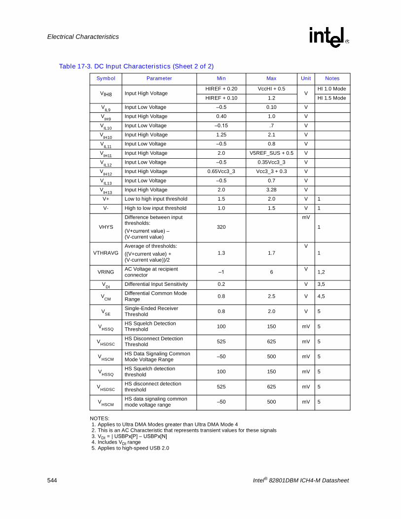
544 Intel® 82801DBM ICH4-M Datasheet
Electrical Characteristics
NOTES:1. Applies to Ultra DMA Modes greater than Ultra DMA Mode 42. This is an AC Characteristic that represents transient values for these signals3. VDI = | USBPx[P] � USBPx[N] 4. Includes VDI range5. Applies to high-speed USB 2.0
VIH8 Input High VoltageHIREF + 0.20 VccHI + 0.5
VHI 1.0 Mode
HIREF + 0.10 1.2 HI 1.5 Mode
VIL9 Input Low Voltage �0.5 0.10 V
VIH9 Input High Voltage 0.40 1.0 V
VIL10 Input Low Voltage �0.15 .7 V
VIH10 Input High Voltage 1.25 2.1 V
VIL11 Input Low Voltage �0.5 0.8 V
VIH11 Input High Voltage 2.0 V5REF_SUS + 0.5 V
VIL12 Input Low Voltage �0.5 0.35Vcc3_3 V
VIH12 Input High Voltage 0.65Vcc3_3 Vcc3_3 + 0.3 V
VIL13 Input Low Voltage �0.5 0.7 V
VIH13 Input High Voltage 2.0 3.28 V
V+ Low to high input threshold 1.5 2.0 V 1
V- High to low input threshold 1.0 1.5 V 1
VHYS
Difference between input thresholds: (V+current value) � (V-current value)
320
mV
1
VTHRAVGAverage of thresholds: ((V+current value) + (V-current value))/2
1.3 1.7V
1
VRING AC Voltage at recipient connector �1 6 V 1,2
VDI Differential Input Sensitivity 0.2 V 3,5
VCMDifferential Common Mode Range 0.8 2.5 V 4,5
VSESingle-Ended Receiver Threshold 0.8 2.0 V 5
VHSSQHS Squelch Detection Threshold 100 150 mV 5
VHSDSCHS Disconnect Detection Threshold 525 625 mV 5
VHSCMHS Data Signaling Common Mode Voltage Range �50 500 mV 5
VHSSQHS Squelch detection threshold 100 150 mV 5
VHSDSCHS disconnect detection threshold 525 625 mV 5
VHSCMHS data signaling common mode voltage range �50 500 mV 5
Table 17-3. DC Input Characteristics (Sheet 2 of 2)
Symbol Parameter Min Max Unit Notes

Intel® 82801DBM ICH4-M Datasheet 545
Electrical Characteristics
NOTE: 1. These signals are open drain.
Table 17-4. DC Characteristic Output Signal Association
Symbol Associated Signals
VOH1/VOL1
IDE Signals: PDD[15:0], SDD[15:0], PDIOW#/PDSTOP, SDIOW#/SDSTOP, PDIOR#/PDWSTB/PRDMARDY, SDIOR#/STWSTB/SRDMARDY, PDDACK#, SDDACK#, PDA[2:0], SDA[2:0], PDCS[3,1]#, SDCS[3,1]#
VOH2/VOL2CPU Signals: A20M#, CPUPWRGD(1), CPUSLP#, IGNNE#, INIT#, INTR, NMI, SMI#, STPCLK#, DPSLP#
VOH3/VOL3 EEPROM Signals: EE_CS, EE_DOUT, EE_SHCLK
VOH4/VOL4
PCI Signals: GNT5#/GNTB#/GPIO17, GNTA#/GPIO16, AD[31:0], C/BE[3:0]#, PCIRST#, GNT[4:0]#, PAR, DEVSEL#, PERR#, PLOCK#, STOP#, TRDY#, IRDY#, FRAME#, SERR# (1)
LPC/FWH Signals: LAD[3:0]/FWH[3:0], LFRAME#/FWH[4]AC�97 Signals: AC_RST#, AC_SDOUT, AC_SYNCLAN Signals: LAN_RSTSYNC, LAN_TXD[2:0]
VOL5/VOH5SMBus Signals: SMBCLK (1), SMBDATA (1)
System Management Signals: SMLINK[1:0](1)
VOL6/VOH6
Power Management Signals: PME#(1), C3_STAT#, SLP_S1#, SLP_S3#, SLP_S4#, SLP_S5#, STP_CPU#, STP_PCI#, GPIO[22}/CPUPERF#(1), CLKRUN#, DPRSLPVR, SSMUXSEL, SUS_STAT#, SUSCLKGPIO Signals: GPIO[43:32, 28:27, 25]Interrupt Signals: SERIRQ, PIRQ[D:A]# (1), PIRQ[H:E]#/GPIO[5:2](1)
Other Signals: SPKR
VOL7/VOH7 USB Signals: USBP[5:0][P,N] in Low and Full Speed Modes
VOL8/VOH8Zpd/Zpu
Hub Interface Signals: HI[11:0], HI_STB / HI_STBS, HI_STB# / HI_STBF
VOL9/VOH9 Interrupt Signals: APICD[1:0] (1)
VHSOI VHSOH VHSOL
VCHIRPJVCHIRPK
USB Signals: USBP[5:0][P:N] in High Speed Modes

546 Intel® 82801DBM ICH4-M Datasheet
Electrical Characteristics
NOTES:1. The CPUPWRGD, SERR#, PME#, PIRQ[A:H], CPUPERF#, APIC[1:0], SMBDATA, SMBCLK and
SMLINK[1:0] signal has an open drain driver, and the VOH spec does not apply. This signal must have external pull up resistor.
2. The condition for the Terminator High Voltage is ZPU = ZTARG(VccHI/VSWING � 1).3. The condition for the Output High Voltage is ZPD = ZTARG.
Table 17-5. DC Output Characteristics
Symbol Parameter Min Max Unit IOL / IOH Notes
VOL1 Output Low Voltage 0.51 V 6 mAVOH1 Output High Voltage Vcc3_3 � 0.51 V �6 mAVOL2 Output Low Voltage �0.15 0.25(V_CPU_IO) V 1.5 mAVOH2 Output High Voltage 0.9(V_CPU_IO) V �0.5 mA 1VOL3 Output Low Voltage 0.4 V 6 mA
VOH3 Output High Voltage 2.4 V �1 mA 1VOL4 Output Low Voltage 0.55 V 6 mAVOH4 Output High Voltage 0.9Vcc3_3 V �0.5 mA 1VOL5 Output Low Voltage 0.4 V 4.0 mAVOH5 Output High Voltage N/A V 1VOL6 Output Low Voltage 0.4 V 4.0 mAVOH6 Output High Voltage Vcc3_3 � 0.5 V �2.0 mA 1VOL7 Output Low Voltage 0.4 V 5 mAVOH7 Output High Voltage Vcc3_3 � 0.5 V �2 mA
VOL8 Output Low Voltage0.1(VccHI) V 1 mA HI 1.0 Mode
0.05 V 1 mA HI 1.5 Mode
VOH8 Output High Voltage
0.9(VccHI) V �1 mA HI 1.0 Mode
VSWING�50 mV VSWING+50 mV VHI 1.5 ModeTerminator High VoltageNote 2
VSWING�50 mV VSWING+50 mV VHI 1.5 ModeOutput High VoltageNote 3
Zpd Pull Down Impedance38 Ohm Vout =
0.5VccHI HI 1.0 Mode
48 Ohm Vout = 0.7V HI 1.5 Mode
Zpu Pull Up Impedance38 Ohm Vout =
0.5VccHI HI 1.0 Mode
46 Ohm Vout = 0.7V HI 1.5 Mode
VHSOI HS Idle Level �10.0 10.0 mV
VHSOH HS Data Signaling High 360 440 mV
VHSOL HS Data Signaling Low �10.0 10.0 mV
VCHIRPJ Chirp J Level 700 1100 mV
VCHIRPK Chirp K Level �900 �500 mV

Intel® 82801DBM ICH4-M Datasheet 547
Electrical Characteristics
NOTE: Includes APICCLK, CLK14, CLK48, CLK66, LAN_CLK, and PCICLK
Table 17-6. Other DC Characteristics
Symbol Parameter Min Max Unit Notes
V5REF ICH4 Core Well Reference Voltage 4.75 5.25 V
Vcc3_3 I/O Buffer Voltage 3.135 3.465 V
V_CPU_IO CPU Interface Voltage 0.8 1.75 V
Vcc1_5, VccHI(HI 1.5),
VccPLLInternal Logic Voltage 1.425 1.575 V
VccHI(HI 1.0) Internal HI 1.0 Logic Voltage 1.71 1.89 V
HIREF Hub Interface Reference Voltage 0.48(VccHI) 0.52(VccHI) V HI 1.0 Mode
0.343 0.357 V HI 1.5 Mode
V5REF_Sus Suspend Well Reference Voltage 4.75 5.25 V
VccSus3_3 Suspend Well I/O Buffer Voltage 3.135 3.465 V
VccSus1_5 Suspend Well Logic Voltage 1.425 1.575 V
VccLAN3_3 LAN Controller I/O Buffer Voltage 3.135 3.465 V
VccLAN1_5 LAN Controller Logic Voltage 1.425 1.575 V
VccRTCPowered by Coin Cell Battery 2.0 3.3 V
Powered by Power Supply 2.0 3.6 V
VIT+ Hysteresis Input Rising Threshold 1.9 V Applied to USBP[5:0][P,N]
VIT- Hysteresis Input Falling Threshold 1.3 V Applied to USBP[5:0]P,N]
VDI Differential Input Sensitivity 0.2 V |(USBPx+,USBPx-)|
VCM Differential Common Mode Range 0.8 2.5 V Includes VDIVCRS Output Signal Crossover Voltage 1.3 2.0 V
VSE Single Ended Rcvr Threshold 0.8 2.0 V
ILI1 ATA Input Leakage Current �200 200 µA (0 V < VIN < 5V)
ILI2 PCI_3V Hi-Z State Data Line Leakage �10 10 µA (0 V < VIN < 3.3V)
ILI3 PCI_5V Hi-Z State Data Line Leakage �70 70 µA Max VIN = 2.7 V Min VIN = 0.5 V
ILI4 Input Leakage Current - Clock signals �100 +100 µA See Note
CINInput Capacitance - Hub interfaceInput Capacitance - All Other
812
pF FC = 1 MHz
COUT Output Capacitance 12 pF FC = 1 MHz
CI/O I/O Capacitance 12 pF FC = 1 MHz
Typical Value
CL XTAL1 6 pF
CL XTAL2 6 pF

548 Intel® 82801DBM ICH4-M Datasheet
Electrical Characteristics
17.4 AC Characteristics
1
Table 17-7. AC Input Characteristics
Type Signals Maximum Voltage
Pulse Duration Notes
Undershoot INTRUDER#, PWROK, RTCRST#, RSMRST# �0.6 V 20 ns
Rise/Fall Slew Rate INTRUDER#, PWROK, RSMRST# 40 mV/us
Table 17-8. Clock Timings (Sheet 1 of 3)
Sym Parameter Min Max Unit Notes Figure
PCI Clock (PCICLK)
t1 Period 30 33.3 ns Figure 17-1
t2 High Time 12 ns Figure 17-1
t3 Low Time 12 ns Figure 17-1
t4 Rise Time 3 ns Figure 17-1
t5 Fall Time 3 ns Figure 17-1
Oscillator Clock (OSC)
t6 Period 67 70 ns Figure 17-1
t7 High Time 20 Figure 17-1
t8 Low Time 20 ns Figure 17-1
USB Clock (USBCLK)
fclk48 Operating Frequency 48 MHz 1
t9 Frequency Tolerance 500 ppm 2
t10 High Time 7 ns Figure 17-1
t11 Low Time 7 ns Figure 17-1
t12 Rise Time 1.2 ns Figure 17-1
t13 Fall Time 1.2 ns Figure 17-1
SUSCLK
fSUSclk Operating Frequency 32 kHz 6
t14 High Time 10 us 6
t15 Low Time 10 us 6

Intel® 82801DBM ICH4-M Datasheet 549
Electrical Characteristics
SMBus Clock (SMBCLK)
fsmb Operating Frequency 10 16 KHz
t18 High time 4.0 50 us 3 Figure17-17
t19 Low time 4.7 us Figure17-17
t20 Rise time 1000 ns Figure17-17
t21 Fall time 300 ns Figure17-17
Table 17-8. Clock Timings (Sheet 2 of 3)
Sym Parameter Min Max Unit Notes Figure

550 Intel® 82801DBM ICH4-M Datasheet
Electrical Characteristics
NOTES:1. The USBCLK is a 48 MHz that expects a 40/60% duty cycle.2. USBCLK is a pass-thru clock that is not altered by the ICH4. This frequency tolerance specification is
required for USB 1.1 compliance and is affected by external elements such as the clock generator and the system board.
3. The maximum high time (t18 Max) provide a simple guaranteed method for devices to detect bus idle conditions.
4. BITCLK Rise and Fall times are measured from 10%VDD and 90%VDD.5. This specification includes pin-to-pin skew from the clock generator as well as board skew.6. SUSCLK duty cycle can range from 30% minimum to 70% maximum.
I/O APIC Clock (APICCLK)
fioap Operating Frequency 14.32 33.33 MHz
t22 High time 12 36 ns Figure 17-1
t23 Low time 12 36 ns Figure 17-1
t24 Rise time 1.0 5.0 ns Figure 17-1
t25 Fall time 1.0 5.0 ns Figure 17-1
AC�97 Clock (BITCLK)
fac97 Operating Frequency 12.288 MHz
t26 Output Jitter 750 ps
t27 High time 32.56 48.84 ns Figure 17-1
t28 Low time 32.56 48.84 ns Figure 17-1
t29 Rise time 2.0 6.0 ns 4 Figure 17-1
t30 Fall time 2.0 6.0 ns 4 Figure 17-1
Hub Interface Clock
fhi Operating Frequency 66 MHz
t31 High time 6.0 ns Figure 17-1
t32 Low time 6.0 ns Figure 17-1
t33 Rise time 0.25 1.2 ns Figure 17-1
t34 Fall time 0.25 1.2 ns Figure 17-1
t35 CLK66 leads PCICLK 1.0 4.5 ns 5
PCI Clock (PCICLK)
t1 Period 30 33.3 ns Figure 17-1
t2 High Time 12 ns Figure 17-1
Table 17-8. Clock Timings (Sheet 3 of 3)
Sym Parameter Min Max Unit Notes Figure
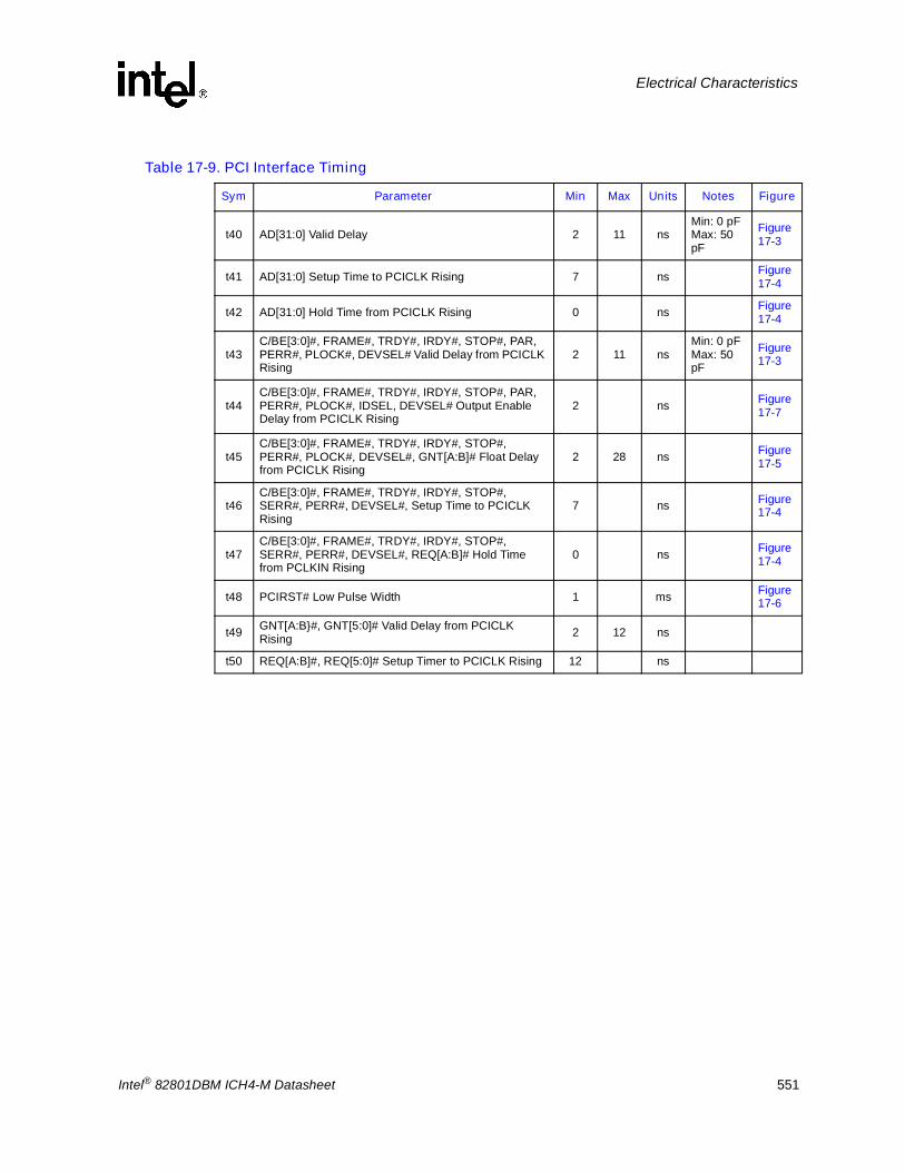
Intel® 82801DBM ICH4-M Datasheet 551
Electrical Characteristics
Table 17-9. PCI Interface Timing
Sym Parameter Min Max Units Notes Figure
t40 AD[31:0] Valid Delay 2 11 nsMin: 0 pFMax: 50 pF
Figure 17-3
t41 AD[31:0] Setup Time to PCICLK Rising 7 ns Figure 17-4
t42 AD[31:0] Hold Time from PCICLK Rising 0 ns Figure 17-4
t43C/BE[3:0]#, FRAME#, TRDY#, IRDY#, STOP#, PAR, PERR#, PLOCK#, DEVSEL# Valid Delay from PCICLK Rising
2 11 nsMin: 0 pFMax: 50 pF
Figure 17-3
t44C/BE[3:0]#, FRAME#, TRDY#, IRDY#, STOP#, PAR, PERR#, PLOCK#, IDSEL, DEVSEL# Output Enable Delay from PCICLK Rising
2 ns Figure 17-7
t45C/BE[3:0]#, FRAME#, TRDY#, IRDY#, STOP#, PERR#, PLOCK#, DEVSEL#, GNT[A:B]# Float Delay from PCICLK Rising
2 28 ns Figure 17-5
t46C/BE[3:0]#, FRAME#, TRDY#, IRDY#, STOP#, SERR#, PERR#, DEVSEL#, Setup Time to PCICLK Rising
7 ns Figure 17-4
t47C/BE[3:0]#, FRAME#, TRDY#, IRDY#, STOP#, SERR#, PERR#, DEVSEL#, REQ[A:B]# Hold Time from PCLKIN Rising
0 ns Figure 17-4
t48 PCIRST# Low Pulse Width 1 ms Figure 17-6
t49 GNT[A:B}#, GNT[5:0]# Valid Delay from PCICLK Rising 2 12 ns
t50 REQ[A:B]#, REQ[5:0]# Setup Timer to PCICLK Rising 12 ns

552 Intel® 82801DBM ICH4-M Datasheet
Electrical Characteristics
NOTES:1. IORDY is internally synchronized. This timing is to guarantee recognition on the next clock.2. PIORDY sample point from DIOx# assertion and PDIOx# active pulse width is programmable from 2�5 PCI
clocks when the drive mode is Mode 2 or greater. Refer to the ISP field in the IDE Timing Register3. PIORDY sample point from DIOx# assertion, PDIOx# active pulse width and PDIOx# inactive pulse width
cycle time is the compatible timing when the drive mode is Mode 0/1. Refer to the TIM0/1 field in the IDE timing register.
4. PDIOx# inactive pulse width is programmable from 1�4 PCI clocks when the drive mode is Mode 2 or greater. Refer to the RCT field in the IDE Timing Register.
Table 17-10. IDE PIO and Multiword DMA ModeTiming
Sym Parameter Min Max Units Notes Figure
t60 PDIOR#/PDIOW#/SDIOR#/SDIOW# Active From CLK66 Rising 2 20 ns Figure 17-8,
Figure 17-9
t61 PDIOR#/PDIOW#/SDIOR#/SDIOW# Inactive From CLK66 Rising 2 20 ns Figure 17-8,
Figure 17-9
t62 PDA[2:0]/SDA[2:0] Valid Delay From CLK66 Rising 2 30 ns Figure 17-8
t63 PDCS1#/SDCS1#, PDCS3#/SDCS3# Active From CLK66 Rising 2 30 ns Figure 17-8
t64 PDCS1#/SDCS1#, PDCS3#/SDCS3# Inactive From CLK66 Rising 2 30 ns Figure 17-8
t65 PDDACK#/SDDACK# Active From CLK66 Rising 2 20 ns Figure 17-9
t66 PDDACK#/SDDACK# Inactive From CLK66 Rising 2 20 ns
t67 PDDREQ/SDDREQ Setup Time to CLK66 Rising 7 ns Figure 17-9
t68 PDDREQ/SDDREQ Hold From CLK66 Rising 7 ns Figure 17-9
t69 PDD[15:0]/SDD[15:0] Valid Delay From CLK66 Rising 2 30 ns Figure 17-8,
Figure 17-9
t70 PDD[15:0]/SDD[15:0] Setup Time to CLK66 Rising 10 ns Figure 17-8,Figure 17-9
t71 PDD[15:0]/SDD[15:0] Hold From CLK66 Rising 7 ns Figure 17-8,Figure 17-9
t72 PIORDY/SIORDY Setup Time to CLK66 Rising 7 ns 1 Figure 17-8
t73 PIORDY/SIORDY Hold From CLK66 Rising 7 ns 1 Figure 17-8
t74 PIORDY/SIORDY Inactive Pulse Width 48 ns Figure 17-8
t75 PDIOR#/PDIOW#/SDIOR#/SDIOW# Pulse Width Low 2,3 Figure 17-8,
Figure 17-9
t76 PDIOR#/PDIOW#/SDIOR#/SDIOW# Pulse Width High 3,4 Figure 17-8,
Figure 17-9

Intel® 82801DBM ICH4-M Datasheet 553
Electrical Characteristics
Table 17-11. Ultra ATA Timing (Mode 0, Mode 1, Mode 2)
Sym Parameter (1)Mode 0 (ns) Mode 1 (ns) Mode 2 (ns) Measuring
Location FigureMin Max Min Max Min Max
t80 Sustained Cycle Time (T2cyctyp) 240 160 120 Sender
Connector
t81 Cycle Time (Tcyc) 112 73 54End Recipient Connector
Figure 17-11
t82 Two Cycle Time (T2cyc) 230 153 115 Sender Connector
Figure 17-11
t83a Data Setup Time (Tds) 15 10 7 Recipient Connector
Figure 17-11
t83bRecipient IC data setup time (from data valid until STROBE edge) (see Note 2) (Tdsic)
14.7 9.7 6.8 ICH4 ball
t84a Data Hold Time (Tdh) 5 5 5 Recipient Connector
Figure 17-11
t84b
Recipient IC data hold time (from STROBE edge until data may become invalid) (see Note 2) (Tdhic)
4.8 4.8 4.8 ICH4 ball
t85a Data Valid Setup Time (Tdvs) 70 48 31 Sender
ConnectorFigure 17-11
t85b
Sender IC data valid setup time (from data valid until STROBE edge) (see Note 2) (Tdvsic)
72.9 50.9 33.9 ICH4 ball
t86a Data Valid Hold Time (Tdvh) 6.2 6.2 6.2 Sender Connector
Figure 17-11
t86b
Sender IC data valid hold time (from STROBE edge until data may become invalid) (see Note 2) (Tdvhic)
9 9 9 ICH4 ball
t87 Limited Interlock Time (Tli) 0 150 0 150 0 150 See Note 2 Figure 17-13
t88 Interlock Time w/ Minimum (Tmli) 20 20 20 Host
ConnectorFigure 17-13
t89 Envelope Time (Tenv) 20 70 20 70 20 70 Host Connector
Figure 17-10
t90 Ready to Pause Time (Trp) 160 125 100 Recipient Connector
Figure 17-12
t91 DMACK setup/hold Time (Tack) 20 20 20 Host
Connector
Figure 17-10,Figure 17-13
t92a CRC Word Setup Time at Host (Tcvs) 70 48 31 Host
Connector

554 Intel® 82801DBM ICH4-M Datasheet
Electrical Characteristics
NOTES:1. The specification symbols in parentheses correspond to the AT Attachment - 6 with Packet Interface
(ATA/ATAPI - 6) specification name.2. See the AT Attachment - 6 with Packet Interface (ATA/ATAPI - 6) Specification for further details on
measuring these timing parameters.
t92b
CRC word valid hold time at sender (from DMACK# negation until CRC may become invalid) (see Note 2) (Tcvh)
6.2 6.2 6.2 Host Connector
t93STROBE output released-to-driving to the first transition of critical timing (Tzfs)
0 0 0 Device Connector
t94Data Output Released-to-Driving Until the First Tunisian of Critical Timing (Tdzfs)
70 48 31 Sender Connector
t95 Unlimited Interlock Time (Tui) 0 0 0 Host
Connector
t96aMaximum time allowed for output drivers to release (from asserted or negated) (Taz)
10 10 10 See Note 2
t96bMinimum time for drivers to assert or negate (from released) (Tzad)
0 0 0 Device Connector
t97
Ready-to-final-STROBE time (no STROBE edges shall be sent this long after negation of DMARDY#) (Trfs)
75 70 60 Sender Connector
t98a Maximum time before releasing IORDY (Tiordyz) 20 20 20 Device
Connector
t98bMinimum time before driving IORDY (see Note 2) (Tziordy)
0 0 0 Device Connector
t99
Time from STROBE edge to negation of DMARQ or assertion of STOP (when sender terminates a burst) (Tss)
50 50 50 Sender Connector
Table 17-11. Ultra ATA Timing (Mode 0, Mode 1, Mode 2)
Sym Parameter (1)Mode 0 (ns) Mode 1 (ns) Mode 2 (ns) Measuring
Location FigureMin Max Min Max Min Max

Intel® 82801DBM ICH4-M Datasheet 555
Electrical Characteristics
Table 17-12. Ultra ATA Timing (Mode 3, Mode 4, Mode 5)
Sym Parameter (1)Mode 3 (ns) Mode 4 (ns) Mode 5 (ns) Measuring
Location FigureMin Max Min Max Min Max
t80 Sustained Cycle Time (T2cyctyp) 90 60 40 Sender
Connector
t81 Cycle Time (Tcyc) 39 25 16.8End Recipient Connector
Figure 17-11
t82 Two Cycle Time (T2cyc) 86 57 38 Sender Connector
Figure 17-11
t83 Data Setup Time (Tds) 7 5 4.0 Recipient Connector
Figure 17-11
t83bRecipient IC data setup time (from data valid until STROBE edge) (see Note 2) (Tdsic)
6.8 4.8 2.3 ICH4 Balls
t84 Data Hold Time (Tdh) 5 5 4.6 Recipient Connector
Figure 17-11
t84b
Recipient IC data hold time (from STROBE edge until data may become invalid) (see Note 2) (Tdhic)
4.8 4.8 2.8 ICH4 Balls
t85 Data Valid Setup Time (Tdvs) 20 6.7 4.8 Sender
ConnectorFigure 17-11
t85b
Sender IC data valid setup time (from data valid until STROBE edge) (see Note 2) (Tdvsic)
22.6 9.5 6.0 ICH4 Balls
t86 Data Valid Hold Time (Tdvh) 6.2 6.2 4.8 Sender Connector
Figure 17-11
t86b
Sender IC data valid hold time (from STROBE edge until data may become invalid) (see Note 2) (Tdvhic)
9.0 9.0 6.0 ICH4 Balls
t87 Limited Interlock Time (Tli) 0 100 0 100 0 75 See Note 2 Figure 17-13
t88 Interlock Time w/ Minimum (Tmli) 20 20 20 Host
ConnectorFigure 17-13
t89 Envelope Time (Tenv) 20 55 20 55 20 50 Host Connector
Figure 17-10
t90 Ready to Pause Time (Trp) 100 100 85 Recipient Connector
Figure 17-12
t91 DMACK setup/hold Time (Tack) 20 20 20 Host
Connector
Figure 17-10,Figure 17-13
t92a CRC Word Setup Time at Host (Tcvs) 20 6.7 10 Host
Connector
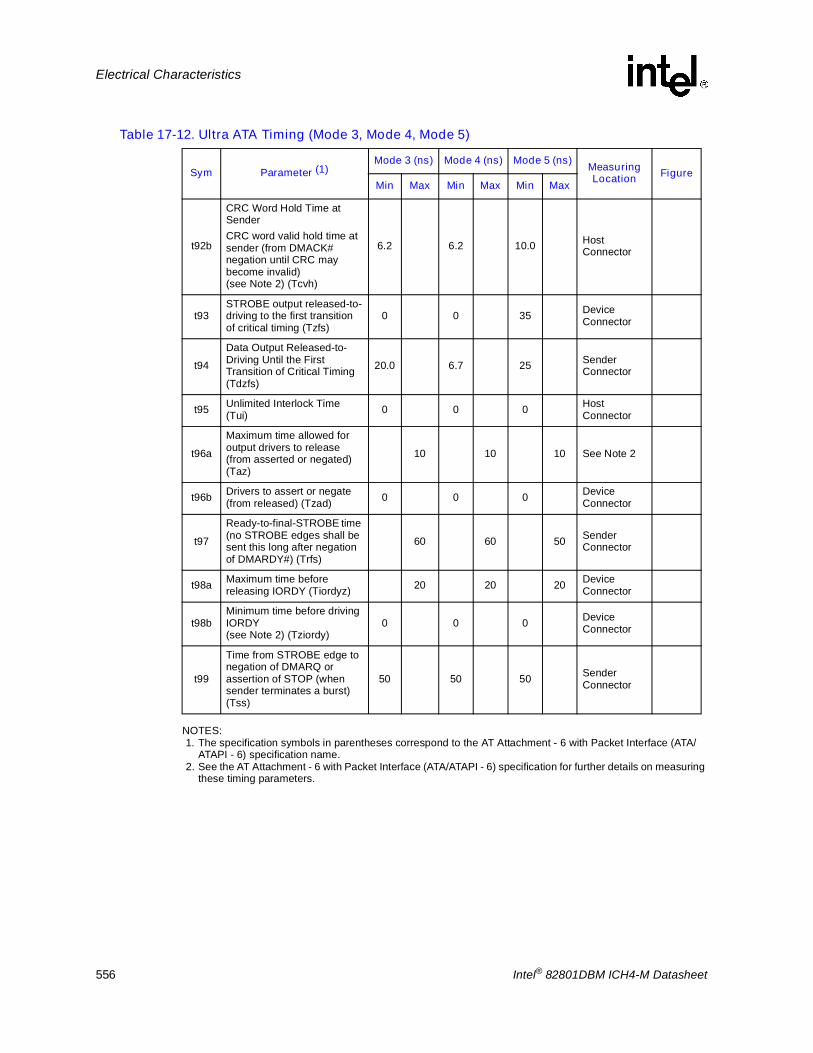
556 Intel® 82801DBM ICH4-M Datasheet
Electrical Characteristics
NOTES:1. The specification symbols in parentheses correspond to the AT Attachment - 6 with Packet Interface (ATA/
ATAPI - 6) specification name.2. See the AT Attachment - 6 with Packet Interface (ATA/ATAPI - 6) specification for further details on measuring
these timing parameters.
t92b
CRC Word Hold Time at SenderCRC word valid hold time at sender (from DMACK# negation until CRC may become invalid) (see Note 2) (Tcvh)
6.2 6.2 10.0 Host Connector
t93STROBE output released-to-driving to the first transition of critical timing (Tzfs)
0 0 35 Device Connector
t94Data Output Released-to-Driving Until the First Transition of Critical Timing (Tdzfs)
20.0 6.7 25 Sender Connector
t95 Unlimited Interlock Time (Tui) 0 0 0 Host
Connector
t96a
Maximum time allowed for output drivers to release (from asserted or negated) (Taz)
10 10 10 See Note 2
t96b Drivers to assert or negate (from released) (Tzad) 0 0 0 Device
Connector
t97
Ready-to-final-STROBE time (no STROBE edges shall be sent this long after negation of DMARDY#) (Trfs)
60 60 50 Sender Connector
t98a Maximum time before releasing IORDY (Tiordyz) 20 20 20 Device
Connector
t98bMinimum time before driving IORDY (see Note 2) (Tziordy)
0 0 0 Device Connector
t99
Time from STROBE edge to negation of DMARQ or assertion of STOP (when sender terminates a burst) (Tss)
50 50 50 Sender Connector
Table 17-12. Ultra ATA Timing (Mode 3, Mode 4, Mode 5)
Sym Parameter (1)Mode 3 (ns) Mode 4 (ns) Mode 5 (ns) Measuring
Location FigureMin Max Min Max Min Max
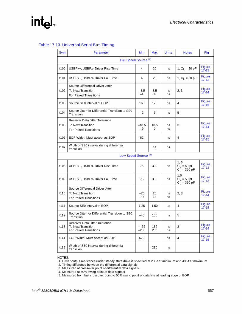
Intel® 82801DBM ICH4-M Datasheet 557
Electrical Characteristics
NOTES:1. Driver output resistance under steady state drive is specified at 28 at minimum and 43 at maximum2. Timing difference between the differential data signals3. Measured at crossover point of differential data signals4. Measured at 50% swing point of data signals5. Measured from last crossover point to 50% swing point of data line at leading edge of EOP
Table 17-13. Universal Serial Bus Timing
Sym Parameter Min Max Units Notes Fig
Full Speed Source (7)
t100 USBPx+, USBPx- Driver Rise Time 4 20 ns 1, CL = 50 pF Figure17-13
t101 USBPx+, USBPx- Driver Fall Time 4 20 ns 1, CL = 50 pF Figure17-13
t102Source Differential Driver JitterTo Next TransitionFor Paired Transitions
�3.5�4
3.54
nsns
2, 3 Figure17-14
t103 Source SE0 interval of EOP 160 175 ns 4 Figure17-15
t104 Source Jitter for Differential Transition to SE0 Transition �2 5 ns 5
t105Receiver Data Jitter ToleranceTo Next TransitionFor Paired Transitions
�18.5�9
18.59
nsns
3 Figure17-14
t106 EOP Width: Must accept as EOP 82 ns 4 Figure17-15
t107 Width of SE0 interval during differential transition 14 ns
Low Speed Source (8)
t108 USBPx+, USBPx- Driver Rise Time 75 300 ns1, 6 CL = 50 pFCL = 350 pF
Figure17-13
t109 USBPx+, USBPx- Driver Fall Time 75 300 ns1,6CL = 50 pFCL = 350 pF
Figure17-13
t110Source Differential Driver JitterTo Next TransitionFor Paired Transitions
�25�14
2514
nsns
2, 3 Figure17-14
t111 Source SE0 interval of EOP 1.25 1.50 µs 4 Figure17-15
t112 Source Jitter for Differential Transition to SE0 Transition �40 100 ns 5
t113Receiver Data Jitter Tolerance To Next TransitionFor Paired Transitions
�152�200
152200
nsns
3 Figure17-14
t114 EOP Width: Must accept as EOP 670 ns 4 Figure17-15
t115 Width of SE0 interval during differential transition 210 ns

558 Intel® 82801DBM ICH4-M Datasheet
Electrical Characteristics
6. Measured from 10% to 90% of the data signal7. Full Speed Data Rate has minimum of 11.97 Mbps and maximum of 12.03 Mbps8. Low Speed Data Rate has a minimum of 1.48 Mbps and a maximum of 1.52 Mbps

Intel® 82801DBM ICH4-M Datasheet 559
Electrical Characteristics
NOTE: The Min AC column indicates the minimum times required by the SMBus and/or I2C specifications. The ICH4 tolerates these timings on both its SMBus and SMLink interfaces.
NOTES:1. A device will timeout when any clock low exceeds this value.2. t137 is the cumulative time a slave device is allowed to extend the clock cycles in one message from the
initial start to stop. If a slave device exceeds this time, it is expected to release both its clock and data lines and reset itself.
3. t138 is the cumulative time a master device is allowed to extend its clock cycles within each byte of a message as defined from start-to-ack, ack-to-ack or ack-to-stop.
4. t134 has a minimum timing for I2C of 0 ns, while the minimum timing for SMBus is 300 ns.
Table 17-14. IOAPIC Bus Timing
Sym Parameter Min Max Units Notes Fig
t120 APICCD[1:0]# Valid Delay from APICCLK Rising 3.0 12.0 ns Figure 17-3
t121 APICCD[1:0]# Setup Time to APICCLK Rising 8.5 ns Figure 17-4
t122 APICCD[1:0]# Hold Time from APICCLK Rising 3.0 ns Figure 17-4
Table 17-15. SMBus Timing
Sym Parameter Min Max Units Notes Fig
t130 Bus Tree Time Between Stop and Start Condition 4.7 µs Figure 17-17
t131 Hold Time after (repeated) Start Condition. After this period, the first clock is generated. 4.0 µs Figure
17-17
t132 Repeated Start Condition Setup Time 4.7 µs Figure 17-17
t133 Stop Condition Setup Time 4.0 µs Figure 17-17
t134 Data Hold Time 0 ns 4 Figure 17-17
t135 Data Setup Time 250 ns Figure 17-17
t136 Device Time Out 25 35 ms 1
t137 Cumulative Clock Low Extend Time (slave device) 25 ms 2 Figure 17-17
t138 Cumulative Clock Low Extend Time (master device) 10 ms 3 Figure 17-17

560 Intel® 82801DBM ICH4-M Datasheet
Electrical Characteristics
Table 17-16. AC�97 Timing
Sym Parameter Min Max Units Notes Fig
t140 ACSDIN[2:0] Setup to Falling Edge of BITCLK 10 ns Figure17-25
t141 ACSDIN[2:0] Hold from Falling Edge of BITCLK 10 ns Figure17-25
t142 ACSYNC, ACSDOUT valid delay from rising edge of BITCLK 15 ns Figure
17-25

Intel® 82801DBM ICH4-M Datasheet 561
Electrical Characteristics
Table 17-17. LPC Timing
Sym Parameter Min Max Units Notes Fig
t150 LAD[3:0] Valid Delay from PCICLK Rising 2 11 ns Figure 17-3
t151 LAD[3:0] Output Enable Delay from PCICLK Rising 2 ns Figure 17-7
t152 LAD[3:0] Float Delay from PCICLK Rising 28 ns Figure 17-5
t153 LAD[3:0] Setup Time to PCICLK Rising 7 ns Figure 17-4
t154 LAD[3:0] Hold Time from PCICLK Rising 0 ns Figure 17-4
t155 LDRQ[1:0]# Setup Time to PCICLK Rising 12 ns Figure 17-4
t156 LDRQ[1:0]# Hold Time from PCICLK Rising 0 ns Figure 17-4
t157 LFRAME# Valid Delay from PCICLK Rising 2 12 ns Figure 17-3
Table 17-18. Miscellaneous Timings
Sym Parameter Min Max Units Notes Fig
t160 SERIRQ Setup Time to PCICLK Rising 7 ns Figure17-4
t161 SERIRQ Hold Time from PCICLK Rising 0 ns Figure17-4
t162 RI#, EXTSMI#, GPI, USB Resume Pulse Width 2 RTCCLK Figure17-6
t163 SPKR Valid Delay from OSC Rising 200 ns Figure17-3
t164 SERR# Active to NMI Active 200 ns
t165 IGNNE# Inactive from FERR# Inactive 230 ns

562 Intel® 82801DBM ICH4-M Datasheet
Electrical Characteristics
NOTES:1. Refer to V5REF/Vcc3_3 sequencing requirements, See Section 2.20.3 for details.2. The VccSus supplies must never be active while the VccRTC supply is inactive. Likewise, the Vcc or
VccLAN supplies must never be active while the VccSus supplies are inactive, and the Vcc supplies must never be active while the VccLAN supplies are inactive.
Table 17-19. Power Sequencing and Reset Signal Timings
Sym Parameter Min Max Units Notes Fig
t170 VccRTC active to RTCRST# inactive 18 � ms Figure 17-18
t171 V5RefSus active to VccSus3_3, VccSus1_5 active 0 � ms 1 Figure 17-18
t172 VccRTC supply active to VccSus supplies active 0 � ms 2 Figure 17-18
t173 VccSus supplies active to RSMRST# high (inactive) 10 � ms
Figure 17-18Figure 17-19
t174 V5Ref active to Vcc3_3, Vcc1_5, V_CPU_IO, VccHI active 0 � ms 1 Figure 17-18
t175a VccSus supplies active to VccLAN supplies active 0 � ms 2 Figure 17-18
t175b VccLAN supplies active to LAN_RST# active 10 � ms Figure 17-18Figure 17-19
t175c VccLAN supplies active to Vcc supplies active 0 � ms Figure 17-18
t176Vcc3_3, Vcc1_5, V_CPU_IO and VccHI supplies active to PWROK, or VRMPWRGD/VGATE
10 � msFigure 17-18Figure 17-19
t177 PWROK and VGATE active and SYS_RESET#inactive to SUS_STAT# inactive 32 38 RTCCLK Figure 17-19
t178 SUS_STAT# inactive to PCIRST# inactive 1 3 RTCCLK Figure 17-19
t179 AC_RST# active low pulse width 1 us
t180 AC_RST# inactive to BIT_CLK startup delay 162.8 ns

Intel® 82801DBM ICH4-M Datasheet 563
Electrical Characteristics
Table 17-20. Power Management Timings (Sheet 1 of 2)
Sym Parameter Min Max Units Notes Fig
t181 VccSus active to SLP_S5#, SUS_STAT# and PCIRST# active 50 ns Figure 17-19
t182t183
RSMRST# inactive to SUSCLK running, SLP_S5# inactive 110 ms 7 Figure 17-19
t183a SLPS5# inactive to SLP_S4# inactive 1 2 RTCCLK Figure 17-19
t183b SLPS4# inactive to SLP_S3# inactive 1 2 RTCCLK Figure 17-19
t184V_CPU_IO to STPCLK#, CPUSLP#, STP_CPU#, STP_PCI#, SLP_S1#, C3_STAT# inactive and processor Frequency Strap signals high
50 ns Figure 17-19, Figure 17-21
t185PWROK and VRMPWRGD/VGATE active and SYS_RESET# inactive to SUS_STAT# inactive and processor Frequency Straps latched to Strap Values
32 38 RTCCLK 1 Figure 17-19
t186 Processor Reset Complete to Frequency Strap signals unlatched from Strap Values 7 9 CLK66 2 Figure 17-19
t187 STPCLK# active to Stop Grant cycle N/A N/A 3 Figure 17-20, Figure 17-21
t188a Stop Grant cycle to C3_STAT# active 0 6 PCICLK 4Figure 17-20,Figure 17-21, Figure 17-24
t188b C3_STAT# active to CPUSLP# active 2.8 µsFigure 17-20Figure 17-21Figure 17-24
t190 CPUSLP# inactive to STPCLK# inactive 3.87 245 µs Figure 17-20,
Figure 17-24
t192a CPUSLP# active to STP_CPU# and DPSLP# active 16 PCICLK 4Figure 17-20, Figure 17-21Figure 17-23Figure 17-24
t192b STP_CPU# active to SUS_STAT# active 2 4 RTCCLK 1 Figure 17-20, Figure 17-21
t193a SUS_STAT# active to STP_PCI# active 2 10 RTCCLK 1 Figure 17-20, Figure 17-21
t193b STP_PCI# active to SLP_S1# active 2 4 RTCCLK 1 Figure 17-20, Figure 17-21
t193c SLP_S1# active to PCIRST# active, STP_PCI# inactive, SLP_S!# inactive, and STP_CPU# inactive 5 7 RTCCLK 1 Figure 17-21
t194 PCIRST# active to SLP_S3# active 1 2 RTCCLK 1 Figure 17-21
t194a SLP_S3# active to SLP_S4# active 1 2 RTCCLK 1 Figure 17-21
t195 SLP_S4# active to SLP_S5# active 1 2 RTCCLK 1, 6 Figure 17-21
t196 SLP_S3# active to PWROK, VRMPWRGD inactive 0 ms 5 Figure 17-21
t197 PWROK, VRMPWRGD inactive to Vcc supplies inactive 20 ns Figure 17-21
t198 Wake Event to SLP_S5# inactive 1 10 RTCCLK 1 Figure 17-21
t198a Wake Event to SLP_S4# inactive (S4 Wake) 1 10 RTCCLK 1 Figure 17-20
t198b Wake Event to SLP_S3# inactive (S3 Wake) 1 10 RTCCLK 1
t198c Wake Event to SLP_S1# inactive 1 10 RTCCLK 1
t198d SLP_S5# inactive to SLP_S4# inactive 1 2 RTCCLK 1

564 Intel® 82801DBM ICH4-M Datasheet
Electrical Characteristics
NOTES:1. These transitions are clocked off the internal RTC. 1 RTC clock is approximately 32 µs.2. This transition is clocked off the 66 MHz CLK66. 1 CLK66 is approximately 15 ns.3. The ICH4 STPCLK# assertion will trigger the processor to send a stop grant acknowledge cycle. The timing
for this cycle getting to the ICH4 is dependant on the processor and the memory controller.4. These transitions are clocked off the 33 MHz PCICLK. 1 PCICLK is approximately 30 ns.5. The ICH4 has no maximum timing requirement for this transition. It is up to the system designer to determine
if the SLP_S3#, SLP_S4# and SLP_S5# signals are used to control the power planes.6. If the transition to S5 is due to Power Button Override, SLP_S3#, SLP_S4# and SLP_S5# are asserted
together similar to timing t194 (PCIRST# active to SLP_S3# active).7. If there is no RTC battery in the system, so VccRTC and the VccSus supplies come up together, the delay
from RTCRST# and RSMRST# inactive to SUSCLK toggling may be as much as 2.5 seconds.
t198e SLP_S4# inactive to SLP_S3# inactive 1 2 RTCCLK 1
t199 SLP_S1# inactive to STP_CPU#, STP_PCI# inactive 3 6.2 ms Figure 17-20
t200 STP_CPU#, STP_PCI# inactive to SUS_STAT# inactive 7 10 ms Figure 17-20
t201 SUS_STAT# inactive to CPU_SLP# inactive 2 4 PCICLK 4 Figure 17-20
t203 STPCLK# inactive to C3_STAT# inactive 0 15 nsFigure 17-20Figure 17-23Figure 17-24
t204 CPU I/F signals latched prior to STPCLK# active 0 4 CLK66 2Figure 17-22, Figure 17-23, Figure 17-24
t205 Break Event to STPCLK# inactive 30 3120 ns Figure 17-22
t206 STPCLK# inactive to processor I/F signals unlatched 240 188
0 nsFigure 17-22, Figure 17-23, Figure 17-24
t207 Break Event to STP_CPU# (for C3 exit) or DPRSLPVR (for C4 exit) inactive 0 8 PCICLK 4 Figure 17-23,
Figure 17-24
t208 STP_CPU# and DPSLP# inactive to CPU_SLP# inactive 30 45 µs 8 Figure 17-23,
Figure 17-24
t209 DPSLP# active to DPRSLPVR active 10 13 µs Figure 17-24
t210 DPRSLPVR inactive to DPSLP# inactive 95 101 µs Figure 17-24
t211 SLP_S1# inactive to DPRSLPVR inactive 2 3 ms
t212 STP_CPU# to processor clock stopped Note: This is a clock generator spec. 0 � PCI CLK Figure 17-26
t213 STP_CPU# inactive to processor clock running. Note: This is a clock generator spec. 0 3 PCI CLK Figure 17-26
t214 STP_CPU# active to SSMUXSEL transition. 9.5 11 µs Figure 17-26
t215 DPSLP# active to start of VGATE ignore time. 0 0 Figure 17-26
t216VGATE ignore time after SSMUXSEL transition (VGATE allowed to go high or low). VGATE must be high at end of ignore time.
95 101 µs Figure 17-26
t217 SSMUXSEL to STP_CPU# High 95 101 µs Figure 17-26
t218 SLP_S1# to PCICLK stop 200 ns Figure 17-26
t219 SLP_S1# inactive to PCICLK running 1.8 ms Figure 17-26
t220 THRMTRIP# active to SLP_S3#, SLP_S4#, SLP_S5# active 2 PCI CLK
Table 17-20. Power Management Timings (Sheet 2 of 2)
Sym Parameter Min Max Units Notes Fig

Intel® 82801DBM ICH4-M Datasheet 565
Electrical Characteristics
8. This value is programmable in multiples of 1024 PCI CLKs. Maximum is 8192 PCI CLKs (245.6 µs).
17.5 Timing Diagrams
Figure 17-1. Clock Timing
Figure 17-2. Valid Delay from Rising Clock Edge
Figure 17-3. Setup and Hold Times
2.0V
0.8V
PeriodHigh Time
Low Time
Fall Time Rise Time
Clock 1.5V
Valid Delay
VTOutput
Clock
VTInput
Hold TimeSetup Time
VT
1.5V

566 Intel® 82801DBM ICH4-M Datasheet
Electrical Characteristics
Figure 17-4. Float Delay
Figure 17-5. Pulse Width
Figure 17-6. Output Enable Delay
Input VT
Output
FloatDelay
VT
Pulse Width
VT
Clock
Output
OutputEnableDelay
VT
1.5V

Intel® 82801DBM ICH4-M Datasheet 567
Electrical Characteristics
Figure 17-7. IDE PIO Mode
Figure 17-8. IDE Multiword DMA
t62,t63 t64
DA[2:0], CS1#, CS3#
t75
t69 t69
t70
t71
t72
t73
t61
read data
CLK66
DIOx#
DD[15:0] Write
DD[15:0] Read
IORDY
t60 t76
write data
sample point
t74
CLK66
idedma.vsd
t67
DDREQ[1:0]
DDACK[1:0]
t65
DIOx#
DD[15:0] Read
DD[15:0] Write
t60 t61t75 t76
t70 t71
t69 t69
Read Data
Write Data Write Data
Read Data
t68

568 Intel® 82801DBM ICH4-M Datasheet
Electrical Characteristics
Figure 17-9. Ultra ATA Mode (Drive Initiating a Burst Read)
Figure 17-10. Ultra ATA Mode (Sustained Burst)
DMARQ(drive)
t91
t89
t89
DMACK# (host)
STOP(host)
DMARDY#(host)
STROBE(drive)
DD[15:0]
DA[2:0], CS[1:0]
t96
t98
t94t95
t85 t86t97
t99b
STROBE @ sender
t81
Data @ sender
t86
t85
t86
t85
t81
t82
t86
STROBE @ receiver
Data @ receiver
t84
t83
t84
t83
t84t99e t99e t99e
t99d t99d
t99g t99g t99g
t99f t99f

Intel® 82801DBM ICH4-M Datasheet 569
Electrical Characteristics
Figure 17-11. Ultra ATA Mode (Pausing a DMA Burst)
Figure 17-12. Ultra ATA Mode (Terminating a DMA Burst)
Figure 17-13. USB Rise and Fall Times
t90
STROBE
DATA
STOP (host)
DMARDY#
t99
t88
STOP(host)
Strobe(host)
DMARDY#(drive)
DATA(host)
DMACK# (host)
t91
t87
DMARQ(drive)
CRC
t99c
t87
t99a
t91t92 t93
DifferentialData Lines
90%
10% 10%
90%
tR tF
Rise Time Fall Time
CL
CL
Low Speed: 75 ns at CL = 50 pF, 300 ns at CL = 350 pFFull Speed: 4 to 20 ns at CL = 50 pFHigh Speed: 0.8 to 1.2 ns at CL = 10 pF

570 Intel® 82801DBM ICH4-M Datasheet
Electrical Characteristics
Figure 17-14. USB Jitter
Figure 17-15. USB EOP Width
Figure 17-16. SMBus Transaction
PairedTransitions
ConsecutiveTransitions
CrossoverPoints
T period
DifferentialData Lines
Jitter
DifferentialData Lines
EOPWidth
DataCrossover
Level
Tperiod
t130
SMBCLK
SMBDATA
t131
t19
t134
t20t21
t135t132 t18
t133

Intel® 82801DBM ICH4-M Datasheet 571
Electrical Characteristics
Figure 17-17. SMBus Timeout
Figure 17-18. Power Sequencing and Reset Signal Timings
Start Stopt137
CLKack CLKack
t138 t138
SMBCLK
SMBDATA
VccRTC
VccSus3_3,VccSus1_5
V5RefSus
RTCRST#
RSMRST#
T170
T171
T172T173
T174
T176
PW RO K,VG ATE
Vcc3_3, Vcc1_5,VCCHI,
V_CPU_IO
V5Ref
VccLAN3_3,VccLAN1_5
LAN_PW RO K
T175a
T175b
T175c
ICH4_Powerup_Reset_MO.vst
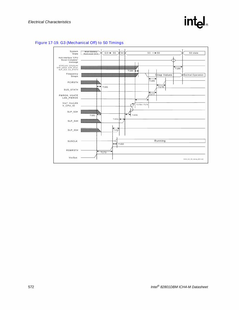
572 Intel® 82801DBM ICH4-M Datasheet
Electrical Characteristics
Figure 17-19. G3 (Mechanical Off) to S0 Timings
S LP _S 3#
V cc*, V ccLA NV _C P U _IO
P W R O K , V G AT ELAN _P W R O K
S U S _S TA T#
P C IR S T#
FrequencyS traps
S T P C L K # , C P U S L P #S T P _ C P U # , S T P _ P C I# ,
S L P _ S 1 # , C 3 _ S T A T #
Hu b interfa ce "CPURe set Com plete"
m essa ge
S ystemS tate
R unn ing
S trap V a lues N orm a l O pera tion
T173
T177
T178T181
T 181
T182
T 184
T185
T 186
S 3 S0 S 0 sta teG 3 S 5 S 4
T 1 8 3
T 1 8 3 a
T 1 8 3b
T 1 7 5 b / T 17 6
M ain BatteryRem oved (G 3 )
ICH 2_G 3_S0_ tim ing_M O .vsdV ccSus
S U S C LK
R S M R ST #
S LP_S 4#
S LP_S 5#

Intel® 82801DBM ICH4-M Datasheet 573
Electrical Characteristics
Figure 17-20. S0 to S1-M to S0 Timing
ich2_S0_S1M_timing.vsd
STATE
STPCLK#
PCI Stop GrantCycle
CPUSLP#
Wake Event
SLP_S1#
C3_STAT#
STP_CPU#DPSLP#
SUS_STAT#
STP_PCI#
S0 S0 S1 S1 S1 S0 S0
T187
T198a
T188a
T188b
T192a
T192b
T193a
T193b
T199
T200
T201
T190
T203
DPRSLPVRT211

574 Intel® 82801DBM ICH4-M Datasheet
Electrical Characteristics
Figure 17-21. S0 to S5 to S0 Timings
Figure 17-22. C0 to C2 to C0 Timings
CPUSLP#
SUS_STAT#
PCIRST#
SLP_S3#
SLP_S5#
Wake Event
PWROK,VGATE
Vcc
S0 S0 S3 S3 S5 S3/S4/S5 S0 S0
T195
T196
T197
T198
T176
T177
T178
T184
SLP_S1#
STPCLK#
Stop GrantCycle
C3_STAT#
STP_CPU#
T187
T188a
T188b
T192a
T192b
T193a
T193b
T194a
T193c
STP_PCI#
S4
SLP_S4#
T194b
Unlatched Latched UnlatchedCPU I/FSignals
STPCLK#
BreakEvent
T204 T205 T206

Intel® 82801DBM ICH4-M Datasheet 575
Electrical Characteristics
Figure 17-23. C0 to C3 to C0 Timings
Figure 17-24. C0 to C4 to C0 Timings
Unlatched Latched UnlatchedCPU I/FSignals
STPCLK#
ICH2_C0_C3_Timing.vsd
BreakEvent
PCI StopGrant Cycle
C3_STAT#
CPU_SLP#
STP_CPU#
T204
T188a
T188b
T192a
T207
T208
T190 T206
T203
Unlatched Latched UnlatchedCPU I/FSignals
STPCLK#
ICH2_C0_C4_Timing.vsd
BreakEvent
PCI StopGrant Cycle
C3_STAT#
CPU_SLP#
STP_CPU#
T204
T188a
T188b
T192a
T207
T208
T190 T206
T203
DPRSLPVR
DPSLP#
T209 T210

576 Intel® 82801DBM ICH4-M Datasheet
Electrical Characteristics
Figure 17-25. AC�97 Data Input and Output Timings
Figure 17-26. Intel® Speedstep® Technology Timing Sequence
VOH
VOL
AC_SDOUTAC_SDIN[2:0]
AC_SYNC
AC_BIT_CLK VI H VI L
tco
thold
tsetup
STPCLK#
PCI StopGrant Cycle
C3_STAT#
CPU_SLP#
STP_CPU#
T188a
T188b
T192a
T208
T190
T203
SSMUXSEL Current New
T214
T217
T215VGATE
Running RunningT212 T213CPU CLK
T216

Intel® 82801DBM ICH4-M Datasheet 577
Package Information
18 Package Information
Figure 18-1 and Figure 18-2 illustrate the ICH4-M 421 BGA package. All dimensions are in millimeters.
Figure 18-1. Intel® ICH4-M Package (Top and Side Views)
Pin A1 Identifier
Pin A1 corner
31.00 ±0.20
26.00 ±0.25
Top View
45° Chamfer(4 places)
16.96 REF
0.127 A -A-
-B-
0.127 A
16.96 REF
26.00 ±0.25
31.00 ±0.20
3 X C1.00 Thru
0.61 ±0.06
Side View
Seating Plane (see Note 3)
-C-
30°
0.60 ±0.10
1.17 ±0.052.38 ±0.21
0.15
0.15 C
Notes:1. All dimensions are in millimeters.2. All dimensions and tolerances conform to ANSI Y14.5M - 1982.3. Primary Datum (-C-) and seating plane are defined by the sperical crowns of the solder balls.
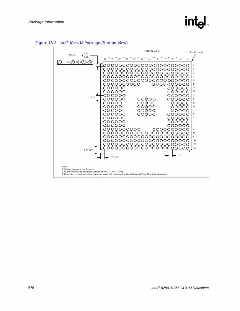
578 Intel® 82801DBM ICH4-M Datasheet
Package Information
Figure 18-2. Intel® ICH4-M Package (Bottom View)
Pin A1 cornerBottom View
A
B
C
D
E
FG
H
JK
L
P
R
T
U
V
Y
ABAA
N
W
M
210162022 35791113151719 121 4618 81214
Notes:1. All dimensions are in millimeters.2. All dimensions and tolerances conform to ANSI Y14.5M - 1982.3. Dimension is measured at the maximum solder ball diameter. Parallel to Datum (-C-) on Side View illustration.
1.53 REF
1.53 REF
1.27
0.90 0.60
Note 3
SBSACS 0.30
1.27
23
AC

Intel® 82801DBM ICH4-M Datasheet 579
Testability
19 Testability
19.1 Test Mode DescriptionThe ICH4-M supports two types of test modes, a tri-state test mode and a XOR Chain test mode. Driving RTCRST# low for a specific number of PCI clocks while PWROK is high will activate a particular test mode as described in Table 19-1.
Note: RTCRST# can be driven low any time after PCIRST# is inactive..
Figure 19-1 illustrates the entry into a test mode. A particular test mode is entered on the rising edge of RTCRST# after being asserted for a specific number of PCI clocks while PWROK is active. To change test modes, the same sequence should be followed again. To restore the ICH4 to normal operation, execute the sequence with RTCRST# being asserted so that no test mode is selected as specified in Table 19-1.
NOTE: After driving RTCRST# low, should wait 0.1 ms before clocking the testmode with PCICLK. It may take up to 2 PCICLKS after RTCRST# is brought high to enter the test mode.
Table 19-1. Test Mode Selection
Number of PCI Clocks RTCRST# Driven Low After PWROK Active Test Mode
<4 No Test Mode Selected
4 XOR Chain 1
5 XOR Chain 2
6 XOR Chain 3
7 XOR Chain 4
8 All �Z�
9�13 Reserved. DO NOT ATTEMPT
14 Long XOR
15�42 Reserved. DO NOT ATTEMPT
43�51 No Test Mode Selected
52 XOR Chain 6
53 XOR Chain 4 Bandgap
>53 No Test Mode Selected
Figure 19-1. Test Mode Entry (XOR Chain Example)
RSMRST#
PWROK
RTCRST#
Other SignalOutputs
N Number of PCI Clocks Test Mode Entered
All Output Signals Tri-Stated XOR Chain Output Enabled

580 Intel® 82801DBM ICH4-M Datasheet
Testability
19.2 Tri-State ModeWhen in the tri-state mode, all outputs and bi-directional pin are tri-stated, including the XOR chain outputs.
19.3 XOR Chain ModeIn the ICH4, provisions for Automated Test Equipment (ATE) board level testing are implemented with XOR chains. The ICH4 signals are grouped into four independent XOR chains which are enabled individually. When an XOR chain is enabled, all output and bi-directional buffers within that chain are tri-stated, except for the XOR chain output. Every signal in the enabled XOR chain (except for the XOR chain�s output) functions as an input. All output and bi-directional buffers for pins not in the selected XOR chain are tri-stated. Figure 19-2 is a schematic example of XOR chain circuitry.
19.3.1 XOR Chain Testability Algorithm ExampleXOR chain testing allows motherboard manufacturers to check component connectivity (e.g., opens and shorts to VCC or GND). An example algorithm to do this is shown in Table 19-2.
In this example, Vector 1 applies all 0s to the chain inputs. The outputs being non-inverting, will consistently produce a 1 at the XOR output on a good board. One short to VCC (or open floating to VCC) will result in a 0 at the chain output, signaling a defect.
Figure 19-2. Example XOR Chain Circuitry
InputPin 2
Vcc
InputPin 1
InputPin 3
InputPin 4
InputPin 5
InputPin 6
XORChainOutput
Table 19-2. XOR Test Pattern Example
Vector InputPin 1
InputPin 2
InputPin 3
InputPin 4
InputPin 5
InputPin 6
XOR Output
1 0 0 0 0 0 0 1
2 1 0 0 0 0 0 03 1 1 0 0 0 0 14 1 1 1 0 0 0 0
5 1 1 1 1 0 0 16 1 1 1 1 1 0 07 1 1 1 1 1 1 1
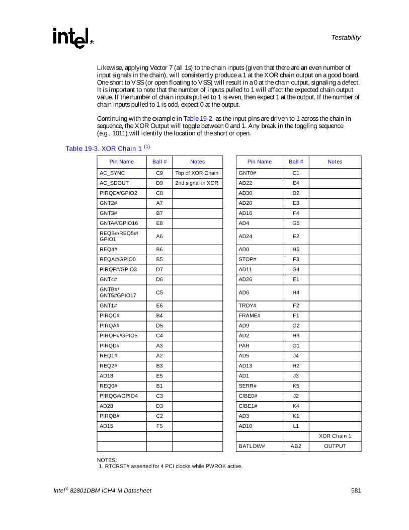
Intel® 82801DBM ICH4-M Datasheet 581
Testability
Likewise, applying Vector 7 (all 1s) to the chain inputs (given that there are an even number of input signals in the chain), will consistently produce a 1 at the XOR chain output on a good board. One short to VSS (or open floating to VSS) will result in a 0 at the chain output, signaling a defect. It is important to note that the number of inputs pulled to 1 will affect the expected chain output value. If the number of chain inputs pulled to 1 is even, then expect 1 at the output. If the number of chain inputs pulled to 1 is odd, expect 0 at the output.
Continuing with the example in Table 19-2, as the input pins are driven to 1 across the chain in sequence, the XOR Output will toggle between 0 and 1. Any break in the toggling sequence (e.g., 1011) will identify the location of the short or open.
NOTES:1. RTCRST# asserted for 4 PCI clocks while PWROK active.
Table 19-3. XOR Chain 1 (1)
Pin Name Ball # Notes Pin Name Ball # Notes
AC_SYNC C9 Top of XOR Chain GNT0# C1
AC_SDOUT D9 2nd signal in XOR AD22 E4
PIRQE#/GPIO2 C8 AD30 D2
GNT2# A7 AD20 E3
GNT3# B7 AD16 F4
GNTA#/GPIO16 E8 AD4 G5
REQB#/REQ5#/GPIO1 A6 AD24 E2
REQ4# B6 AD0 H5
REQA#/GPIO0 B5 STOP# F3
PIRQF#/GPIO3 D7 AD11 G4
GNT4# D6 AD26 E1
GNTB#/GNT5#GPIO17 C5 AD6 H4
GNT1# E6 TRDY# F2
PIRQC# B4 FRAME# F1
PIRQA# D5 AD9 G2
PIRQH#/GPIO5 C4 AD2 H3
PIRQD# A3 PAR G1
REQ1# A2 AD5 J4
REQ2# B3 AD13 H2
AD18 E5 AD1 J3
REQ0# B1 SERR# K5
PIRQG#/GPIO4 C3 C/BE0# J2
AD28 D3 C/BE1# K4
PIRQB# C2 AD3 K1
AD15 F5 AD10 L1
XOR Chain 1
BATLOW# AB2 OUTPUT

582 Intel® 82801DBM ICH4-M Datasheet
Testability
NOTES:1. RTCRST# asserted for 5 PCI clocks while PWROK active.
Table 19-4. XOR Chain 2 (1)
Pin Name Ball # Notes Pin Name Ball # Notes
AD8 K2 Top of XOR Chain GPIO7 R3
IRDY# L5 2nd signal in XOR LAD0/FWH0 T2
PERR# L4 LAD1/FWH1 R4
AD14 L3 C3_STAT# T3
AD12 L2 LDRQ0# U3
AD23 M5 LAD2/FWH2 T4
C/BE2# M4 LAD3/FWH3 U2
DEVSEL# M3 LDRQ1# U4
PLOCK# M2 LFRAME# / FWH4 T5
AD17 N1 THRM# V1
AD19 N2 AC_BIT_CLK B8
AD21 N3 REQ3# C7
C/BE3# N4 AD7 J5
AD25 P1 GPIO8 V4
AD27 P2 RI# Y1
AD29 R1 AC_SDIN0 D13
AD31 P4 AC_SDIN2 B13
AGPBUSY# R2 AC_SDIN1 A13
PCICLK P5
XOR Chain 2
BATLOW# AB2 OUTPUT

Intel® 82801DBM ICH4-M Datasheet 583
Testability
NOTES:1. RTCRST# asserted for 6 PCI clocks while PWROK active.
Table 19-5. XOR Chain 3 (1)
Pin Name Ball # Notes Pin Name Ball # Notes
PDD10 AC9 Top of XOR Chain INTR AB22
PDDREQ AA11 2nd signal in XOR NMI V21
PDD12 AB10 IGNNE# W21
PDD14 W11 INIT# V22
PDD1 AC11 STPCLK# V23
PDD15 Y11 SMI# W23
PDD0 AB11 CPUSLP# U21
PDIOR# AC12 DPSLP# U23
PIORDY AB12 HI_STB#/HI_STBF N20
PDDACK# Y12 HI_STB/HI_STBS P21
PDIOW# W12 SSMUXSEL J21
IRQ14 AC13 GPIO32 J20
PDA1 AB13 GPIO33 G22
PDA0 AA13 GPIO37 H20
PDCS1# Y13 GPIO35 G20
PDA2 W13 GPIO36 F21
PDCS3# AB14 GPIO34 F20
IRQ15 AA19 PDD6 Y8
SLP_S1# W18 PDD4 AA7
STP_PCI# Y21 PDD7 AA8
CPUPERF# Y20 PDD11 W9
STP_CPU# W19 PDD5 AB8
VGATE/VRMPWRGD V19 PDD8 AB9
A20GATE Y22 PDD9 Y9
RCIN# U22 PDD13 W10
DPRSLPVR V20 PDD2 Y10
THRMTRIP# W20 PDD3 AA10
A20M# AB23 INTRUDER# W6
CPUPWRGD Y23 SLP_S5# AA2
XOR Chain 3
RI# Y1 OUTPUT

584 Intel® 82801DBM ICH4-M Datasheet
Testability
NOTES:
1. RTCRST# asserted for 7 PCI clocks while PWROK active. 2
Table 19-6. XOR Chain 4-1 (1)
Pin Name Ball # Notes Pin Name Ball # Notes
SDD8 Y14 Top of XOR Chain HI4 P19
SDD3 AC16 2nd signal in XOR HICOMP R23
SDD6 W14 HI_STB#/HI_STBF N20
SDD10 AA15 HI_STB/HI_STBS P21
SDD12 AB16 HI3 M21
SDD11 Y15 HI2 M19
SDD1 AB17 HI1 L20
SDD4 W15 HI0 L19
SDD13 Y16 HI10 N22
SDDREQ AB18 HI8 P23
SDD14 AA17 HI9 L22
SDDACK# AB19 HI11 K21
SIORDY AC19 APICD1 K20
SDA1 AC20 SERIRQ J22
SDD15 Y17 APICCLK J19
SDD2 W16 APICD0 H19
SDA2 AC21 CLK14 J23
SDIOW# AA18 SPKR H23
SDD0 W17 GPIO41 H21
SDCS1# AB21 GPIO39 H22
SDIOR# Y18 GPIO40 G23
SDCS3# AC22 GPIO38 F23
SDA0 AA20 GPIO42 F22
FERR# AA21 GPIO43 E23
CLK66 T21 SDD7 AA14
HI6 T20 SDD9 AC15
HI5 R19 SDD5 AB15
HI7 R20 SLP_S4# Y2
XOR Chain 4-1
GPIO8 V4 OUTPUT

Intel® 82801DBM ICH4-M Datasheet 585
Testability
NOTES:1. RTCRST# asserted for 7 PCI clocks while PWROK active.
2
NOTES:1. RTCRST# asserted for 52 PCI clocks while PWROK active.
2
Table 19-7. XOR Chain 4-2 (1)
Pin Name Ball # Notes Pin Name Ball # Notes
PME# W2 Top of XOR Chain AC_RST# C13
GPIO25 V2 2nd signal in XOR USBP0P C20
GPIO12 V5 USBP0N D20
GPIO27 W1 USBP1P A21
PCIRST# U5 USBP1N B21
GPIO13 W3 USBP2P C18
GPIO28 W4 USBP2N D18
PWRBTN# AA1 USBP3P A19
SYS_RESET# Y3 USBP3N B19
SMLINK1 AB1 USBP4P C16
BATLOW# AB2 USBP4N D16
CLKRUN# AC2 USBP5P A17
SUSCLK AA4 USBP5N B17
SUS_STAT#/LPCPD# AB3 LAN_TXD2 A12
SMLINK0 AC3 LAN_CLK C11
SLP_S3# Y4 EE_DIN D11
SMBDATA AB4 LAN_RXD2 A11
SMBCLK AC4 LAN_RSTSYNC B11
SMBALERT#/GPIO11 AA5 EE_CS D10
CLK48 F19 LAN_TXD0 B10
OC0# B15 LAN_RXD0 A10
OC2# A15 LAN_TXD1 C10
OC5# D14 EE_DOUT A8
OC1# C14 LAN_RXD1 A9
OC3# B14 EE_SHCLK C12
OC4# A14
XOR Chain 4-2 AC_SDIN1 A13 OUTPUT
Table 19-8. XOR Chain 6 (1)
Pin Name Ball # Notes Pin Name Ball # Notes
RTCX1 AC7 Top of XOR Chain
XOR Chain 6BATLOW# AB2 OUTPUT

586 Intel® 82801DBM ICH4-M Datasheet
Testability
Table 19-9. LONG XOR Chain(1) (Sheet 1 of 3)
Pin Name Ball # Notes Pin Name Ball # Notes
AC_SYNC C9 Top of XOR Chain PDA0 AA13
AC_SDOUT D9 2nd signal in XOR PDCS1# Y13
PIRQE#/GPIO2 C8 PDA2 W13
GNT2# A7 PDCS3# AB14
GNT3# B7 IRQ15 AA19
GNTA#/GPIO16 E8 SLP_S1# W18
REQB#/REQ5#/GPIO1 A6 STP_PCI# Y21
REQ4# B6 CPUPERF# Y20
REQA#/GPIO0 B5 STP_CPU# W19
PIRQF#/GPIO3 D7 VGATE/VRMPWRGD V19
GNT4# D6 A20GATE Y22
GNTB#/GNT5#GPIO17 C5 RCIN# U22
GNT1# E6 DPRSLPVR V20
PIRQC# B4 THRMTRIP# W20
PIRQA# D5 A20M# AB23
PIRQH#/GPIO5 C4 CPUPWRGD Y23
PIRQD# A3 INTR AB22
REQ1# A2 NMI V21
REQ2# B3 IGNNE# W21
AD18 E5 INIT# V22
REQ0# B1 STPCLK# V23
PIRQG#/GPIO4 C3 SMI# W23
AD28 D3 CPUSLP# U21
PIRQB# C2 DPSLP# U23
AD15 F5 HI_STB#/HI_STBF N20
GNT0# C1 HI_STB/HI_STBS P21
AD22 E4 SSMUXSEL J21
AD30 D2 GPIO32 J20
AD20 E3 GPIO33 G22
AD16 F4 GPIO37 H20
AD4 G5 GPIO35 G20
AD24 E2 GPIO36 F21
AD0 H5 GPIO34 F20
STOP# F3 PDD6 Y8
AD11 G4 PDD4 AA7

Intel® 82801DBM ICH4-M Datasheet 587
Testability
AD26 E1 PDD7 AA8
AD6 H4 PDD11 W9
TRDY# F2 PDD5 AB8
FRAME# F1 PDD8 AB9
AD9 G2 PDD9 Y9
AD2 H3 PDD13 W10
PAR G1 PDD2 Y10
AD5 J4 PDD3 AA10
AD13 H2 PME# W2
AD1 J3 GPIO25 V2
SERR# K5 GPIO12 V5
C/BE0# J2 GPIO27 W1
C/BE1# K4 PCIRST# U5
AD3 K1 GPIO13 W3
AD10 L1 GPIO28 W4
AD8 K2 PWRBTN# AA1
IRDY# L5 SYS_RESET# Y3
PERR# L4 SMLINK1 AB1
AD14 L3 BATLOW# AB2
AD12 L2 CLKRUN# AC2
AD23 M5 SUSCLK AA4
C/BE2# M4 SUS_STAT#/LPCPD# AB3
DEVSEL# M3 SMLINK0 AC3
PLOCK# M2 SLP_S3# Y4
AD17 N1 SMBDATA AB4
AD19 N2 SMBCLK AC4
AD21 N3 SMBALERT#/GPIO11 AA5
C/BE3# N4 CLK48 F19
AD25 P1 OC0# B15
AD27 P2 OC2# A15
AD29 R1 OC5# D14
AD31 P4 OC1# C14
AGPBUSY# R2 OC3# B14
PCICLK P5 OC4# A14
GPIO7 R3 AC_RST# C13
LAD0/FWH0 T2 USBP0P C20
Table 19-9. LONG XOR Chain(1) (Sheet 2 of 3)
Pin Name Ball # Notes Pin Name Ball # Notes
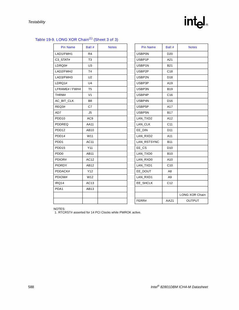
588 Intel® 82801DBM ICH4-M Datasheet
Testability
NOTES:1. RTCRST# asserted for 14 PCI Clocks while PWROK active.
LAD1/FWH1 R4 USBP0N D20
C3_STAT# T3 USBP1P A21
LDRQ0# U3 USBP1N B21
LAD2/FWH2 T4 USBP2P C18
LAD3/FWH3 U2 USBP2N D18
LDRQ1# U4 USBP3P A19
LFRAME# / FWH4 T5 USBP3N B19
THRM# V1 USBP4P C16
AC_BIT_CLK B8 USBP4N D16
REQ3# C7 USBP5P A17
AD7 J5 USBP5N B17
PDD10 AC9 LAN_TXD2 A12
PDDREQ AA11 LAN_CLK C11
PDD12 AB10 EE_DIN D11
PDD14 W11 LAN_RXD2 A11
PDD1 AC11 LAN_RSTSYNC B11
PDD15 Y11 EE_CS D10
PDD0 AB11 LAN_TXD0 B10
PDIOR# AC12 LAN_RXD0 A10
PIORDY AB12 LAN_TXD1 C10
PDDACK# Y12 EE_DOUT A8
PDIOW# W12 LAN_RXD1 A9
IRQ14 AC13 EE_SHCLK C12
PDA1 AB13
LONG XOR Chain
FERR# AA21 OUTPUT
Table 19-9. LONG XOR Chain(1) (Sheet 3 of 3)
Pin Name Ball # Notes Pin Name Ball # Notes

Intel® 82801DBM ICH4-M Datasheet 589
Register Index
A Register Index
Table A-1. Intel® ICH4 PCI Configuration Registers (Sheet 1 of 10)
Register Name Offset Datasheet Location
LAN Controller (B1:D8:F0)
Vendor Identification 00�01h Section 7.1.1, �VID�Vendor ID Register (LAN Controller�B1:D8:F0)� on page 7-266
Device Identification 02�03h Section 7.1.2, �DID�Device ID Register (LAN Controller�B1:D8:F0)� on page 7-266
PCI Command 04�05h Section 7.1.3, �PCICMD�PCI Command Register (LAN Controller�B1:D8:F0)� on page 7-267
PCI Device Status 06�07h Section 7.1.4, �PCISTS�PCI Status Register (LAN Controller�B1:D8:F0)� on page 7-268
Revision Identification 08h Section 7.1.5, �REVID�Revision ID Register (LAN Controller�B1:D8:F0)� on page 7-269
Sub Class Code 0Ah Section 7.1.6, �SCC�Sub-Class Code Register (LAN Controller�B1:D8:F0)� on page 7-269
Base Class Code 0Bh Section 7.1.7, �BCC�Base-Class Code Register (LAN Controller�B1:D8:F0)� on page 7-269
Cache Line Size 0Ch Section 7.1.8, �CLS�Cache Line Size Register (LAN Controller�B1:D8:F0)� on page 7-269
Master Latency Timer 0Dh Section 7.1.9, �PMLT�PCI Master Latency Timer Register (LAN Controller�B1:D8:F0)� on page 7-270
Header Type 0Eh Section 7.1.10, �HEADTYP�Header Type Register (LAN Controller�B1:D8:F0)� on page 7-270
CSR Memory-Mapped Base Address 10�13h Section 7.1.11, �CSR_MEM_BASE CSR � Memory-Mapped Base Address Register (LAN Controller�B1:D8:F0)� on page 7-270
CSR I/O-Mapped Base Address 14�17h Section 7.1.12, �CSR_IO_BASE � CSR I/O-Mapped Base Address Register (LAN Controller�B1:D8:F0)� on page 7-271
Subsystem Vendor ID 2C�2Dh Section 7.1.13, �SVID � Subsystem Vendor ID (LAN Controller�B1:D8:F0)� on page 7-271
Subsystem ID 2E�2Fh Section 7.1.14, �SID � Subsystem ID (LAN Controller�B1:D8:F0)� on page 7-271
Capabilities Pointer 34h Section 7.1.15, �CAP_PTR � Capabilities Pointer (LAN Controller�B1:D8:F0)� on page 7-272
Interrupt Line Register 3Ch Section 7.1.16, �INT_LN � Interrupt Line Register (LAN Controller�B1:D8:F0)� on page 7-272
Interrupt Pin Register 3Dh Section 7.1.17, �INT_PN � Interrupt Pin Register (LAN Controller�B1:D8:F0)� on page 7-272
Minimum Grant Register 3Eh Section 7.1.18, �MIN_GNT � Minimum Grant Register (LAN Controller�B1:D8:F0)� on page 7-272
Maximum Latency Register 3Fh Section 7.1.19, �MAX_LAT � Maximum Latency Register (LAN Controller�B1:D8:F0)� on page 7-273

590 Intel® 82801DBM ICH4-M Datasheet
Register Index
Capability ID Register DCh Section 7.1.20, �CAP_ID � Capability ID Register (LAN Controller�B1:D8:F0)� on page 7-273
Next Item Pointer DDh Section 7.1.21, �NXT_PTR � Next Item Pointer (LAN Controller�B1:D8:F0)� on page 7-273
Power Management Capabilities DE�DFh Section 7.1.22, �PM_CAP � Power Management Capabilities (LAN Controller�B1:D8:F0)� on page 7-274
Power Management Control/Status Register E0�E1h Section 7.1.23, �PMCSR � Power Management Control/Status Register
(LAN Controller�B1:D8:F0)� on page 7-274
Data Register E2h Section 7.1.24, �PCIDATA � PCI Power Management Data Register (LAN Controller�B1:D8:F0)� on page 7-275
Hub Interface to PCI Bridge D30:F0
Vendor ID 00�01h Section 8.1.1, �VID�Vendor ID Register (HUB-PCI�D30:F0)� on page 8-290
Device ID 02�03h Section 8.1.2, �DID�Device ID Register (HUB-PCI�D30:F0)� on page 8-290
PCI Device Command Register 04�05h Section 8.1.3, �CMD�Command Register (HUB-PCI�D30:F0)� on page 8-291
PCI Device Status Register 06�07h Section 8.1.4, �PD_STS�Primary Device Status Register (HUB-PCI�D30:F0)� on page 8-292
Revision ID 08h Section 8.1.5, �RID�Revision Identification Register (HUB-PCI�D30:F0)� on page 8-293
Sub Class Code 0Ah Section 8.1.6, �SCC�Sub-Class Code Register (HUB-PCI�D30:F0)� on page 8-293
Base Class Code 0Bh Section 8.1.7, �BCC�Base-Class Code Register (HUB-PCI�D30:F0)� on page 8-293
Primary Master Latency Timer 0Dh Section 8.1.8, �PMLT�Primary Master Latency Timer Register (HUB-PCI�D30:F0)� on page 8-293
Header Type 0Eh Section 8.1.9, �HEADTYP�Header Type Register (HUB-PCI�D30:F0)� on page 8-294
Primary Bus Number 18h Section 8.1.10, �PBUS_NUM�Primary Bus Number Register (HUB-PCI�D30:F0)� on page 8-294
Secondary Bus Number 19h Section 8.1.11, �SBUS_NUM�Secondary Bus Number Register (HUB-PCI�D30:F0)� on page 8-294
Subordinate Bus Number 1Ah Section 8.1.12, �SUB_BUS_NUM�Subordinate Bus Number Register (HUB-PCI�D30:F0)� on page 8-294
Secondary Master Latency Timer 1Bh Section 8.1.13, �SMLT�Secondary Master Latency Timer Register (HUB-PCI�D30:F0)� on page 8-295
IO Base Register 1Ch Section 8.1.14, �IOBASE�I/O Base Register (HUB-PCI�D30:F0)� on page 8-295
IO Limit Register 1Dh Section 8.1.15, �IOLIM�I/O Limit Register (HUB-PCI�D30:F0)� on page 8-295
Secondary Status Register 1E�1Fh Section 8.1.16, �SECSTS�Secondary Status Register (HUB-PCI�D30:F0)� on page 8-296
Memory Base 20�21h Section 8.1.17, �MEMBASE�Memory Base Register (HUB-PCI�D30:F0)� on page 8-297
Memory Limit 22�23h Section 8.1.18, �MEMLIM�Memory Limit Register (HUB-PCI�D30:F0)� on page 8-297
Table A-1. Intel® ICH4 PCI Configuration Registers (Sheet 2 of 10)
Register Name Offset Datasheet Location

Intel® 82801DBM ICH4-M Datasheet 591
Register Index
Prefetchable Memory Base 24�25h Section 8.1.19, �PREF_MEM_BASE�Prefetchable Memory Base Register (HUB-PCI�D30:F0)� on page 8-297
Prefetchable Memory Limit 26�27h Section 8.1.20, �PREF_MEM_MLT�Prefetchable Memory Limit Register (HUB-PCI�D30:F0)� on page 8-298
I/O Base Upper 16 Bits 30�31h Section 8.1.21, �IOBASE_HI�I/O Base Upper 16 Bits Register (HUB-PCI�D30:F0)� on page 8-298
I/O Limit Upper 16 Bits 32�33h Section 8.1.22, �IOLIM_HI�I/O Limit Upper 16 Bits Register (HUB-PCI�D30:F0)� on page 8-298
Interrupt Line 3Ch Section 8.1.23, �INT_LINE�Interrupt Line Register (HUB-PCI�D30:F0)� on page 8-298
Bridge Control 3E�3Fh Section 8.1.24, �BRIDGE_CNT�Bridge Control Register (HUB-PCI�D30:F0)� on page 8-299
Hub Interface 1 Command Control Register 40�43h Section 8.1.25, �HI1_CMD�Hub Interface 1 Command Control Register
(HUB-PCI�D30:F0)� on page 8-300
Secondary PCI Device Hiding Register 44�45h Section 8.1.26, �DEVICE_HIDE�Secondary PCI Device Hiding Register (HUB-PCI�D30:F0)� on page 8-301
ICH4 Configuration Register 50�51h Section 8.1.27, �CNF�ICH4 Configuration Register (HUB-PCI�D30:F0)� on page 8-302
Multi-Transaction Timer 70h Section 8.1.28, �MTT�Multi-Transaction Timer Register (HUB-PCI�D30:F0)� on page 8-302
PCI Master Status 82h Section 8.1.29, �PCI_MAST_STS�PCI Master Status Register (HUB-PCI�D30:F0)� on page 8-303
Error Command Register 90h Section 8.1.30, �ERR_CMD�Error Command Register (HUB-PCI�D30:F0)� on page 8-303
Error Status Register 92h Section 8.1.31, �ERR_STS�Error Status Register (HUB-PCI�D30:F0)� on page 8-304
LPC Bridge D31:F0
Vendor ID 00�01h Section 9.1.1, �VID�Vendor ID Register (LPC I/F�D31:F0)� on page 9-306
Device ID 02�03h Section 9.1.2, �DID�Device ID Register (LPC I/F�D31:F0)� on page 9-306
PCI Command Register 04�05h Section 9.1.3, �PCICMD�PCI COMMAND Register (LPC I/F�D31:F0)� on page 9-307
PCI Device Status Register 06�07h Section 9.1.4, �PCISTA�PCI Device Status (LPC I/F�D31:F0)� on page 9-308
Revision ID 08h Section 9.1.5, �REVID�Revision ID Register (LPC I/F�D31:F0)� on page 9-308
Programming Interface 09h Section 9.1.6, �PI�Programming Interface (LPC I/F�D31:F0)� on page 9-309
Sub Class Code 0Ah Section 9.1.7, �SCC�Sub-Class Code Register (LPC I/F�D31:F0)� on page 9-309
Base Class Code 0Bh Section 9.1.8, �BCC�Base-Class Code Register (LPC I/F�D31:F0)� on page 9-309
Header Type 0Eh Section 9.1.9, �HEADTYP�Header Type Register (LPC I/F�D31:F0)� on page 9-309
ACPI Base Address Register 40�43h Section 9.1.10, �PMBASE�ACPI Base Address (LPC I/F�D31:F0)� on page 9-310
Table A-1. Intel® ICH4 PCI Configuration Registers (Sheet 3 of 10)
Register Name Offset Datasheet Location

592 Intel® 82801DBM ICH4-M Datasheet
Register Index
ACPI Control 44h Section 9.1.11, �ACPI_CNTL�ACPI Control (LPC I/F � D31:F0)� on page 9-310
BIOS Control Register 4E�4Fh Section 9.1.12, �BIOS_CNTL�BIOS Control Register (LPC I/F�D31:F0)� on page 9-311
TCO Control 54h Section 9.1.13, �TCO_CNTL � TCO Control (LPC I/F � D31:F0)� on page 9-311
GPIO Base Address Register 58�5Bh Section 9.1.14, �GPIOBASE�GPIO Base Address (LPC I/F�D31:F0)� on page 9-312
GPIO Control Register 5Ch Section 9.1.15, �GPIO_CNTL�GPIO Control (LPC I/F�D31:F0)� on page 9-312
PIRQ[A:D] Routing Control 60�63h Section 9.1.16, �PIRQ[n]_ROUT�PIRQ[A,B,C,D] Routing Control (LPC I/F�D31:F0)� on page 9-312
Serial IRQ Control Register 64h Section 9.1.17, �SERIRQ_CNTL�Serial IRQ Control (LPC I/F�D31:F0)� on page 9-313
PIRQ[E:H] Routing Control 68�6Bh Section 9.1.18, �PIRQ[n]_ROUT�PIRQ[E,F,G,H] Routing Control (LPC I/F�D31:F0)� on page 9-313
Device 31 Error Config Register 88h Section 9.1.19, �D31_ERR_CFG�Device 31 Error Configuration Register (LPC I/F�D31:F0)� on page 9-314
Device 31 Error Status Register 8Ah Section 9.1.20, �D31_ERR_STS�Device 31 Error Status Register (LPC I/F�D31:F0)� on page 9-314
PCI DMA Configuration Registers 90�91h Section 9.1.21, �PCI_DMA_CFG�PCI DMA Configuration (LPC I/F�D31:F0)� on page 9-315
General Control D0h�D3h Section 9.1.22, �GEN_CNTL � General Control Register (LPC I/F � D31:F0)� on page 9-316
General Status D4h Section 9.1.23, �GEN_STA�General Status Register (LPC I/F�D31:F0)� on page 9-318
Backed Up Control D5h Section 9.1.24, �BACK_CNTL�Backed Up Control Register (LPC I/F�D31:F0)� on page 9-319
Real Time Clock Configuration D8h Section 9.1.25, �RTC_CONF�RTC Configuration Register (LPC I/F�D31:F0)� on page 9-320
LPC COM Port Decode Ranges E0h Section 9.1.26, �COM_DEC�LPC I/F Communication Port Decode Ranges (LPC I/F�D31:F0)� on page 9-320
LPC FDD & LPT Decode Ranges E1h Section 9.1.27, �FDD/LPT_DEC�LPC I/F FDD & LPT Decode Ranges (LPC I/F�D31:F0)� on page 9-321
LPC Sound Decode Ranges E2h Section 9.1.28, �SND_DEC�LPC I/F Sound Decode Ranges (LPC I/F�D31:F0)� on page 9-321
FWH Decode Enable 1 Register E3h Section 9.1.29, �FWH_DEC_EN1�FWH Decode Enable 1 Register (LPC I/F�D31:F0)� on page 9-322
LPC Generic Decode Range 1 E4h�E5h Section 9.1.30, �GEN1_DEC�LPC I/F Generic Decode Range 1 Register (LPC I/F�D31:F0)� on page 9-323
LPC Enables E6h�E7h Section 9.1.31, �LPC_EN�LPC I/F Enables Register (LPC I/F�D31:F0)� on page 9-323
FWH Select 1 Register E8h Section 9.1.32, �FWH_SEL1�FWH Select 1 Register (LPC I/F�D31:F0)� on page 9-325
LPC Generic Decode Range 2 ECh�EDh Section 9.1.33, �GEN2_DEC�LPC I/F Generic Decode Range 2 Register (LPC I/F�D31:F0)� on page 9-326
Table A-1. Intel® ICH4 PCI Configuration Registers (Sheet 4 of 10)
Register Name Offset Datasheet Location

Intel® 82801DBM ICH4-M Datasheet 593
Register Index
FWH Select 2 Register EE�EFh Section 9.1.34, �FWH_SEL2�FWH Select 2 Register (LPC I/F�D31:F0)� on page 9-326
FWH Decode Enable 2 Register F0h Section 9.1.35, �FWH_DEC_EN2�FWH Decode Enable 2 Register (LPC I/F�D31:F0)� on page 9-327
Function Disable Register F2h Section 9.1.36, �FUNC_DIS�Function Disable Register (LPC I/F�D31:F0)� on page 9-328
General Power Management Configuration 1 A0h Section 9.8.1.1, �GEN_PMCON_1�General PM Configuration 1 Register
(PM�D31:F0)� on page 9-362
General Power Management Configuration 2 A2h Section 9.8.1.2, �GEN_PMCON_2�General PM Configuration 2 Register
(PM�D31:F0)� on page 9-363
General Power Management Configuration 3 A4h Section 9.8.1.3, �GEN_PMCON_3�General PM Configuration 3 Register
(PM�D31:F0)� on page 9-364
Stop Clock Delay Register A8h Section 9.8.1.4, �STPCLK_DEL�Stop Clock Delay Register (PM�D31:F0)� on page 9-365
GPI_ROUT B8�BBh Section 9.8.1.5, �GPI_ROUT�GPI Routing Control Register (PM�D31:F0)� on page 9-365
I/O Monitor Trap Forwarding Enable Register C0h Section 9.8.1.6, �TRP_FWD_EN�IO Monitor Trap Forwarding Enable
Register (PM�D31:F0)� on page 9-366
I/O Monitor [4:7] Trap Range Registers C4h, C6h, C8h, CAh
Section 9.8.1.7, �MON[n]_TRP_RNG�I/O Monitor [4:7] Trap Range Register for Devices 4�7 (PM�D31:F0)� on page 9-367
I/O Monitor [4:7] Trap Mask Register CCh Section 9.8.1.8, �MON_TRP_MSK�I/O Monitor Trap Range Mask Register for Devices 4�7 (PM�D31:F0)� on page 9-367
IDE Controller (D31:F1)
Vendor ID 00h�01h Section 10.1.1, �VID�Vendor ID Register (LPC I/F�D31:F1)� on page 10-402
Device ID 02h�03h Section 10.1.2, �DID�Device ID Register (LPC I/F�D31:F1)� on page 10-402
Command Register 04h�05h Section 10.1.3, �CMD � Command Register (IDE�D31:F1)� on page 10-402
Device Status 06h�07h Section 10.1.4, �STS � Device Status Register (IDE�D31:F1)� on page 10-403
Revision ID Register 08h Section 10.1.5, �REVID�Revision ID Register (IDE�D31:F1)� on page 10-403
Programming Interface 09h Section 10.1.6, �PI � Programming Interface Register (IDE�D31:F1)� on page 10-404
Sub Class Code 0Ah Section 10.1.7, �SCC � Sub Class Code Register (IDE�D31:F1)� on page 10-404
Base Class Code 0Bh Section 10.1.8, �BCC � Base Class Code Register (IDE�D31:F1)� on page 10-404
Master Latency Timer 0Dh Section 10.1.9, �MLT � Master Latency Timer Register (IDE�D31:F1)� on page 10-405
Primary Command Block Base Address Register 10�13h Section 10.1.10, �PCMD_BAR�Primary Command Block Base Address
Register (IDE�D31:F1)� on page 10-405
Primary Control Block Base Address Register 14�17h Section 10.1.11, �PCNL_BAR�Primary Control Block Base Address
Register (IDE�D31:F1)� on page 10-405
Secondary Command Block Base Address Register 18�1Bh Section 10.1.12, �SCMD_BAR�Secondary Command Block Base
Address Register (IDE D31:F1)� on page 10-406
Table A-1. Intel® ICH4 PCI Configuration Registers (Sheet 5 of 10)
Register Name Offset Datasheet Location

594 Intel® 82801DBM ICH4-M Datasheet
Register Index
Secondary Control Block Base Address Register 1C�1Fh Section 10.1.13, �SCNL_BAR�Secondary Control Block Base Address
Register (IDE D31:F1)� on page 10-406
Bus Master Base Address Register 20h�23h Section 10.1.14, �BM_BASE � Bus Master Base Address Register (IDE�D31:F1)� on page 10-406
Expansion Base Address Register 24�27h Section 10.1.15, �EXBAR � Expansion Base Address Register (IDE�D31:F1)� on page 10-407
Subsystem Vendor ID Register 2C�2Dh Section 10.1.16, �IDE_SVID � Subsystem Vendor ID Register (IDE�D31:F1)� on page 10-407
Subsystem ID Register 2E�2Fh Section 10.1.17, �IDE_SID � Subsystem ID Register (IDE�D31:F1)� on page 10-407
Interrupt Line Register 3Ch Section 10.1.18, �INTR_LN�Interrupt Line Register (IDE�D31:F1)� on page 10-408
Interrupt Pin Register 3Dh Section 10.1.19, �INTR_PN�Interrupt Pin Register (IDE�D31:F1)� on page 10-408
IDE Timing Register 40h�43h Section 10.1.20, �IDE_TIM � IDE Timing Register (IDE�D31:F1)� on page 10-408
Slave IDE Timing 44h Section 10.1.21, �SLV_IDETIM�Slave (Drive 1) IDE Timing Register (IDE�D31:F1)� on page 10-410
Synchronous DMA Control Register 48h Section 10.1.22, �SDMA_CNT�Synchronous DMA Control Register (IDE�D31:F1)� on page 10-411
Synchronous DMA Timing Register 4Ah�4Bh Section 10.1.23, �SDMA_TIM�Synchronous DMA Timing Register (IDE�D31:F1)� on page 10-412
IDE I/O Configuration Register 54�57h Section 10.1.24, �IDE_CONFIG�IDE I/O Configuration Register (IDE�D31:F1)� on page 10-413
USB Controller (D31:F0,F1,F2)
Vendor ID 00�01h Section 11.1.1, �VID�Vendor Identification Register (USB�D29:F0/F1/F2)� on page 11-419
Device ID 02�03h Section 11.1.2, �DID�Device Identification Register (USB�D29:F0/F1/F2)� on page 11-420
Command Register 04�05h Section 11.1.3, �CMD�Command Register (USB�D29:F0/F1/F2)� on page 11-420
Device Status 06�07h Section 11.1.4, �STA�Device Status Register (USB�D29:F0/F1/F2)� on page 11-421
Revision ID 08h Section 11.1.5, �RID�Revision Identification Register (USB�D29:F0/F1/F2)� on page 11-421
Programming Interface 09h Section 11.1.6, �PI�Programming Interface (USB�D29:F0/F1/F2)� on page 11-421
Sub Class Code 0Ah Section 11.1.7, �SCC�Sub Class Code Register (USB�D29:F0/F1/F2)� on page 11-422
Base Class Code 0Bh Section 11.1.8, �BCC�Base Class Code Register (USB�D29:F0/F1/F2)� on page 11-422
Header Type Register 0Eh Section 11.1.9, �HTYPE�Header Type Register (USB�D29:F0/F1/F2)� on page 11-422
Base Address Register 20�23h Section 11.1.10, �BASE�Base Address Register (USB�D29:F0/F1/F2)� on page 11-423
Subsystem Vendor ID Register 2C�2Dh Section 11.1.11, �SVID � Subsystem Vendor ID (USB�D29:F0/F1/F2)� on page 11-423
Table A-1. Intel® ICH4 PCI Configuration Registers (Sheet 6 of 10)
Register Name Offset Datasheet Location

Intel® 82801DBM ICH4-M Datasheet 595
Register Index
Subsystem ID Register 2E�2Fh Section 11.1.12, �SID � Subsystem ID (USB�D29:F0/F1/F2)� on page 11-423
Interrupt Line 3Ch Section 11.1.13, �INTR_LN�Interrupt Line Register (USB�D29:F0/F1/F2)� on page 11-424
Interrupt Pin 3Dh Section 11.1.14, �INTR_PN�Interrupt Pin Register (USB�D29:F0/F1/F2)� on page 11-424
Serial Bus Release Number 60h Section 11.1.15, �USB_RELNUM�USB Release Number Register (USB�D29:F0/F1/F2)� on page 11-424
USB Legacy Keyboard/Mouse Control C0�C1h Section 11.1.16, �USB_LEGKEY�USB Legacy Keyboard/Mouse Control Register (USB�D29:F0/F1/F2)� on page 11-425
USB Resume Enable C4h Section 11.1.17, �USB_RES�USB Resume Enable Register (USB�D29:F0/F1/F2)� on page 11-426
USB EHCI Controller (D29:F7)
Command Register 04�05h Section 12.1.3, �PCICMD�PCI Command Register (USB EHCI�D29:F7)� on page 12-439
Device Status 06�07h Section 12.1.4, �PCISTS�PCI Device Status Register (USB EHCI�D29:F7)� on page 12-440
Revision ID 08h Section 12.1.5, �REVID�Revision ID Register (USB EHCI�D29:F7)� on page 12-440
Programming Interface 09h Section 12.1.6, �PI�Programming Interface Register (USB EHCI�D29:F7)� on page 12-441
Sub Class Code 0Ah Section 12.1.7, �SCC�Sub Class Code Register (USB EHCI�D29:F7)� on page 12-441
Base Class Code 0Bh Section 12.1.8, �BCC�Base Class Code Register (USB EHCI�D29:F7)� on page 12-441
Master Latency Timer 0Eh Section 12.1.9, �MLT� PCI Master Latency Timer Register (USB EHCI�D29:F7)� on page 12-441
Memory Base Address Register 10�13h Section 12.1.10, �MEM_BASE�Memory Base Address Register (USB EHCI�D29:F7)� on page 12-442
Subsystem Vendor ID 2C�2Dh Section 12.1.11, �SVID�USB EHCI Subsystem Vendor ID Register (USB EHCI�D29:F7)� on page 12-442
Subsystem ID 2E�2Fh Section 12.1.12, �SID�USB EHCI Subsystem ID Register (USB EHCI�D29:F7)� on page 12-442
Capabilities Pointer 34h Section 12.1.13, �CAP_PTR�Capabilities Pointer Register (USB EHCI�D29:F7)� on page 12-443
Interrupt Line 3Ch Section 12.1.14, �INT_LN�Interrupt Line Register (USB EHCI�D29:F7)� on page 12-443
Interrupt Pin 3Dh Section 12.1.15, �INT_PN�Interrupt Pin Register (USB EHCI�D29:F7)� on page 12-443
Power Management Capability ID 50h Section 12.1.16, �PWR_CAPID�PCI Power Management Capability ID Register (USB EHCI�D29:F7)� on page 12-443
Next Item Ptr 51h Section 12.1.17, �NXT_PTR1�Next Item Pointer #1 Register (USB EHCI�D29:F7)� on page 12-444
Power Mgt Capabilities 52�53h Section 12.1.18, �PWR_CAP�Power Management Capabilities Register (USB EHCI�D29:F7)� on page 12-444
Power Mgt Control/Status 54�55h Section 12.1.19, �PWR_CNTL_STS�Power Management Control/Status Register (USB EHCI�D29:F7)� on page 12-445
Table A-1. Intel® ICH4 PCI Configuration Registers (Sheet 7 of 10)
Register Name Offset Datasheet Location

596 Intel® 82801DBM ICH4-M Datasheet
Register Index
Debug Port Capability ID 58h Section 12.1.20, �DEBUG_CAPID�Debug Port Capability ID Register (USB EHCI�D29:F7)� on page 12-445
Next Item Ptr #2 59h Section 12.1.21, �NXT_PTR2�Next Item Pointer #2 Register (USB EHCI�D29:F7)� on page 12-446
Debug Port Base Offset 5A�5Bh Section 12.1.22, �DEBUG_BASE�Debug Port Base Offset Register (USB EHCI�D29:F7)� on page 12-446
USB Release Number 60h Section 12.1.23, �USB_RELNUM�USB Release Number Register (USB EHCI�D29:F7)� on page 12-446
Frame Length Adjustment 61h Section 12.1.24, �FL_ADJ�Frame Length Adjustment Register (USB EHCI�D29:F7)� on page 12-447
Power Wake Capabilities 62�63h Section 12.1.25, �PWAKE_CAP�Port Wake Capability Register (USB EHCI�D29:F7)� on page 12-447
USB UHCI Port Override 64�65h Section 12.1.26, �PORT_OVRIDE�USB UHCI Port Override Register (USB EHCI�D29:F7)� on page 12-448
USB EHCI Legacy Support Extended Capability 68�6Bh Section 12.1.27, �LEG_EXT_CAP�USB EHCI Legacy Support Extended
Capability Register (USB EHCI�D29:F7)� on page 12-448
USB EHCI Legacy Support Control/Status 6C�6Fh Section 12.1.28, �LEG_EXT_CS�USB EHCI Legacy Support Extended
Control / Status Register (USB EHCI�D29:F7)� on page 12-449
Intel Specific USB EHCI SMI 70�73h Section 12.1.29, �SPECIAL_SMI�Intel Specific USB EHCI SMI Register (USB EHCI�D29:F7)� on page 12-451
Access Control 80h Section 12.1.30, �ACCESS_CNTL�Access Control Register (USB EHCI�D29:F7)� on page 12-452
USB HS Reference Voltage Register DC�DFh Section 12.1.31, �HS_Ref_V�USB HS Reference Voltage Register (USB EHCI�D29:F7)� on page 12-452
SMBus Controller (D31:F3)
Vendor ID 00�01h Section 13.1.1, �VID�Vendor Identification Register (SMBUS�D31:F3)� on page 13-473
Device ID 02�03h Section 13.1.2, �DID�Device Identification Register (SMBUS�D31:F3)� on page 13-474
Command Register 04�05h Section 13.1.3, �CMD�Command Register (SMBUS�D31:F3)� on page 13-474
Device Status 06�07h Section 13.1.4, �STA�Device Status Register (SMBUS�D31:F3)� on page 13-475
Revision ID Register 08h Section 13.1.5, �REVID�Revision ID Register (SMBUS�D31:F3)� on page 13-475
Sub Class Code 0Ah Section 13.1.6, �SCC�Sub Class Code Register (SMBUS�D31:F3)� on page 13-475
Base Class Code 0Bh Section 13.1.7, �BCC�Base Class Code Register (SMBUS�D31:F3)� on page 13-476
SMB Base Address Register 20�23h Section 13.1.8, �SMB_BASE�SMBUS Base Address Register (SMBUS�D31:F3)� on page 13-476
Subsystem Vendor ID Register 2C�2Dh Section 13.1.9, �SVID � Subsystem Vendor ID (SMBUS�D31:F2/F4)� on page 13-476
Subsystem ID Register 2E�2Fh Section 13.1.10, �SID � Subsystem ID (SMBUS�D31:F2/F4)� on page 13-476
Interrupt Line 3Ch Section 13.1.11, �INTR_LN�Interrupt Line Register (SMBUS�D31:F3)� on page 13-477
Table A-1. Intel® ICH4 PCI Configuration Registers (Sheet 8 of 10)
Register Name Offset Datasheet Location

Intel® 82801DBM ICH4-M Datasheet 597
Register Index
Interrupt Pin 3Dh Section 13.1.12, �INTR_PN�Interrupt Pin Register (SMBUS�D31:F3)� on page 13-477
Host Configuration 40h Section 13.1.13, �HOSTC�Host Configuration Register (SMBUS�D31:F3)� on page 13-477
AC�97 Audio Controller (D31:F5)
Vendor Identification 00h�01h Section 14.1.1, �VID�Vendor Identification Register (Audio�D31:F5)� on page 14-490
Device Identification 02h�03h Section 14.1.2, �DID�Device Identification Register (Audio�D31:F5)� on page 14-490
PCI Command 04h�05h Section 14.1.3, �PCICMD�PCI Command Register (Audio�D31:F5)� on page 14-491
PCI Device Status 06h�07h Section 14.1.4, �PCISTS�PCI Device Status Register (Audio�D31:F5)� on page 14-492
Revision Identification 08h Section 14.1.5, �RID�Revision Identification Register (Audio�D31:F5)� on page 14-493
Programming Interface 09h Section 14.1.6, �PI�Programming Interface Register (Audio�D31:F5)� on page 14-493
Sub Class Code 0Ah Section 14.1.7, �SCC�Sub Class Code Register (Audio�D31:F5)� on page 14-493
Base Class Code 0Bh Section 14.1.8, �BCC�Base Class Code Register (Audio�D31:F5)� on page 14-493
Header Type 0Eh Section 14.1.9, �HEDT�Header Type Register (Audio�D31:F5)� on page 14-494
Native Audio Mixer Base Address 10h�13h Section 14.1.10, �NAMBAR�Native Audio Mixer Base Address Register (Audio�D31:F5)� on page 14-494
Native Audio Bus Mastering Base Address 14h�17h Section 14.1.11, �NABMBAR�Native Audio Bus Mastering Base Address
Register (Audio�D31:F5)� on page 14-495
Mixer Base Address(Mem) 18�1Bh Section 14.1.12, �MMBAR�Mixer Base Address Register (Audio�D31:F5)� on page 14-495
Bus Master Base Address(Mem) 1C�1F Section 14.1.13, �MBBAR�Bus Master Base Address Register (Audio�D31:F5)� on page 14-496
Subsystem Vendor ID 2Ch�2Dh Section 14.1.14, �SVID�Subsystem Vendor ID Register (Audio�D31:F5)� on page 14-496
Subsystem ID 2Eh�2Fh Section 14.1.15, �SID�Subsystem ID Register (Audio�D31:F5)� on page 14-497
Capabilities Pointer 34h Section 14.1.16, �CAP_PTR�Capabilities Pointer Register (Audio�D31:F5)� on page 14-497
Interrupt Line 3Ch Section 14.1.17, �INTR_LN�Interrupt Line Register (Audio�D31:F5)� on page 14-497
Interrupt Pin 3Dh Section 14.1.18, �INTR_PN�Interrupt Pin Register (Audio�D31:F5)� on page 14-498
Programmable Codec ID 40h Section 14.1.19, �PCID�Programmable Codec ID Register (Audio�D31:F5)� on page 14-498
Configuration 41h Section 14.1.20, �CFG�Configuration Register (Audio�D31:F5)� on page 14-499
PCI Power Management ID 50�51h Section 14.1.21, �PID�PCI Power Management Capability ID Register (Audio�D31:F5)� on page 14-499
Table A-1. Intel® ICH4 PCI Configuration Registers (Sheet 9 of 10)
Register Name Offset Datasheet Location
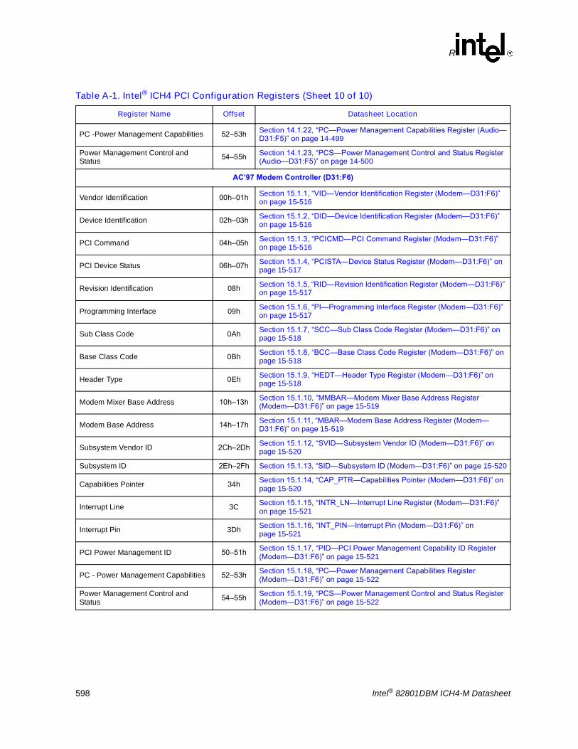
598 Intel® 82801DBM ICH4-M Datasheet
Register Index
PC -Power Management Capabilities 52�53h Section 14.1.22, �PC�Power Management Capabilities Register (Audio�D31:F5)� on page 14-499
Power Management Control and Status 54�55h Section 14.1.23, �PCS�Power Management Control and Status Register
(Audio�D31:F5)� on page 14-500
AC�97 Modem Controller (D31:F6)
Vendor Identification 00h�01h Section 15.1.1, �VID�Vendor Identification Register (Modem�D31:F6)� on page 15-516
Device Identification 02h�03h Section 15.1.2, �DID�Device Identification Register (Modem�D31:F6)� on page 15-516
PCI Command 04h�05h Section 15.1.3, �PCICMD�PCI Command Register (Modem�D31:F6)� on page 15-516
PCI Device Status 06h�07h Section 15.1.4, �PCISTA�Device Status Register (Modem�D31:F6)� on page 15-517
Revision Identification 08h Section 15.1.5, �RID�Revision Identification Register (Modem�D31:F6)� on page 15-517
Programming Interface 09h Section 15.1.6, �PI�Programming Interface Register (Modem�D31:F6)� on page 15-517
Sub Class Code 0Ah Section 15.1.7, �SCC�Sub Class Code Register (Modem�D31:F6)� on page 15-518
Base Class Code 0Bh Section 15.1.8, �BCC�Base Class Code Register (Modem�D31:F6)� on page 15-518
Header Type 0Eh Section 15.1.9, �HEDT�Header Type Register (Modem�D31:F6)� on page 15-518
Modem Mixer Base Address 10h�13h Section 15.1.10, �MMBAR�Modem Mixer Base Address Register (Modem�D31:F6)� on page 15-519
Modem Base Address 14h�17h Section 15.1.11, �MBAR�Modem Base Address Register (Modem�D31:F6)� on page 15-519
Subsystem Vendor ID 2Ch�2Dh Section 15.1.12, �SVID�Subsystem Vendor ID (Modem�D31:F6)� on page 15-520
Subsystem ID 2Eh�2Fh Section 15.1.13, �SID�Subsystem ID (Modem�D31:F6)� on page 15-520
Capabilities Pointer 34h Section 15.1.14, �CAP_PTR�Capabilities Pointer (Modem�D31:F6)� on page 15-520
Interrupt Line 3C Section 15.1.15, �INTR_LN�Interrupt Line Register (Modem�D31:F6)� on page 15-521
Interrupt Pin 3Dh Section 15.1.16, �INT_PIN�Interrupt Pin (Modem�D31:F6)� on page 15-521
PCI Power Management ID 50�51h Section 15.1.17, �PID�PCI Power Management Capability ID Register (Modem�D31:F6)� on page 15-521
PC - Power Management Capabilities 52�53h Section 15.1.18, �PC�Power Management Capabilities Register (Modem�D31:F6)� on page 15-522
Power Management Control and Status 54�55h Section 15.1.19, �PCS�Power Management Control and Status Register
(Modem�D31:F6)� on page 15-522
Table A-1. Intel® ICH4 PCI Configuration Registers (Sheet 10 of 10)
Register Name Offset Datasheet Location
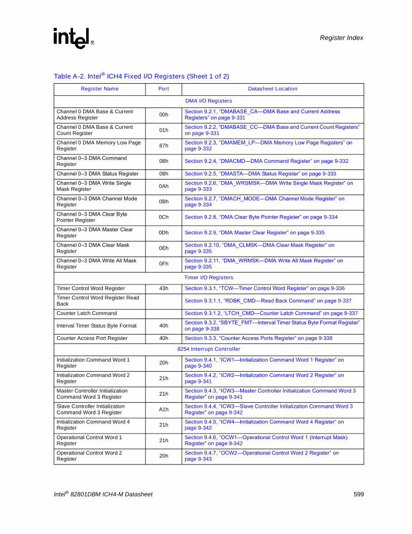
Intel® 82801DBM ICH4-M Datasheet 599
Register Index
Table A-2. Intel® ICH4 Fixed I/O Registers (Sheet 1 of 2)
Register Name Port Datasheet Location
DMA I/O Registers
Channel 0 DMA Base & Current Address Register 00h Section 9.2.1, �DMABASE_CA�DMA Base and Current Address
Registers� on page 9-331
Channel 0 DMA Base & Current Count Register 01h Section 9.2.2, �DMABASE_CC�DMA Base and Current Count Registers�
on page 9-331
Channel 0 DMA Memory Low Page Register 87h Section 9.2.3, �DMAMEM_LP�DMA Memory Low Page Registers� on
page 9-332
Channel 0�3 DMA Command Register 08h Section 9.2.4, �DMACMD�DMA Command Register� on page 9-332
Channel 0�3 DMA Status Register 08h Section 9.2.5, �DMASTA�DMA Status Register� on page 9-333
Channel 0�3 DMA Write Single Mask Register 0Ah Section 9.2.6, �DMA_WRSMSK�DMA Write Single Mask Register� on
page 9-333
Channel 0�3 DMA Channel Mode Register 0Bh Section 9.2.7, �DMACH_MODE�DMA Channel Mode Register� on
page 9-334
Channel 0�3 DMA Clear Byte Pointer Register 0Ch Section 9.2.8, �DMA Clear Byte Pointer Register� on page 9-334
Channel 0�3 DMA Master Clear Register 0Dh Section 9.2.9, �DMA Master Clear Register� on page 9-335
Channel 0�3 DMA Clear Mask Register 0Eh Section 9.2.10, �DMA_CLMSK�DMA Clear Mask Register� on
page 9-335
Channel 0�3 DMA Write All Mask Register 0Fh Section 9.2.11, �DMA_WRMSK�DMA Write All Mask Register� on
page 9-335
Timer I/O Registers
Timer Control Word Register 43h Section 9.3.1, �TCW�Timer Control Word Register� on page 9-336
Timer Control Word Register Read Back Section 9.3.1.1, �RDBK_CMD�Read Back Command� on page 9-337
Counter Latch Command Section 9.3.1.2, �LTCH_CMD�Counter Latch Command� on page 9-337
Interval Timer Status Byte Format 40h Section 9.3.2, �SBYTE_FMT�Interval Timer Status Byte Format Register� on page 9-338
Counter Access Port Register 40h Section 9.3.3, �Counter Access Ports Register� on page 9-338
8254 Interrupt Controller
Initialization Command Word 1 Register 20h Section 9.4.1, �ICW1�Initialization Command Word 1 Register� on
page 9-340
Initialization Command Word 2 Register 21h Section 9.4.2, �ICW2�Initialization Command Word 2 Register� on
page 9-341
Master Controller Initialization Command Word 3 Register 21h Section 9.4.3, �ICW3�Master Controller Initialization Command Word 3
Register� on page 9-341
Slave Controller Initialization Command Word 3 Register A1h Section 9.4.4, �ICW3�Slave Controller Initialization Command Word 3
Register� on page 9-342
Initialization Command Word 4 Register 21h Section 9.4.5, �ICW4�Initialization Command Word 4 Register� on
page 9-342
Operational Control Word 1 Register 21h Section 9.4.6, �OCW1�Operational Control Word 1 (Interrupt Mask)
Register� on page 9-342
Operational Control Word 2 Register 20h Section 9.4.7, �OCW2�Operational Control Word 2 Register� on
page 9-343

600 Intel® 82801DBM ICH4-M Datasheet
Register Index
NOTE: When the POS_DEC_EN bit is set, additional I/O ports get positively decoded by the ICH4. Refer to through for a listing of these ranges.
Operational Control Word 3 Register 20h Section 9.4.8, �OCW3�Operational Control Word 3 Register� on
page 9-344
Master Controller Edge/Level Triggered Register 4D0h Section 9.4.9, �ELCR1�Master Controller Edge/Level Triggered Register�
on page 9-345
Slave Controller Edge/Level Triggered Register 4D1h Section 9.4.10, �ELCR2�Slave Controller Edge/Level Triggered Register�
on page 9-346
Processor Interface Registers
NMI Status and Control Register 61h Section 9.7.1, �NMI_SC�NMI Status and Control Register� on page 9-358
NMI Enable Register 70h Section 9.7.2, �NMI_EN�NMI Enable (and Real Time Clock Index) Register� on page 9-359
PORT92 � Fast A20 and Init Register 92h Section 9.7.3, �PORT92�Fast A20 and Init Register� on page 9-359
Coprocessor Error Register F0h Section 9.7.4, �COPROC_ERR�Coprocessor Error Register� on page 9-359
Reset Control Register CF9h Section 9.7.5, �RST_CNT�Reset Control Register� on page 9-360
APM I/O Decode Registers
Advanced Power Management Control Port Register B2h Section 9.8.2.1, �APM_CNT�Advanced Power Management Control Port
Register� on page 9-368
Advanced Power Management Status Port Register B3h Section 9.8.2.2, �APM_STS�Advanced Power Management Status Port
Register� on page 9-368
PIO Mode Registers
PIO Mode Command Block Offset for Secondary Drive 170h�177h See ATA Specification for detailed register description
PIO Mode Command Block Offset for Primary Drive 1F0h�1F7h See ATA Specification for detailed register description
PIO Mode Control Block Offset for Secondary Drive 376h See ATA Specification for detailed register description
PIO Mode Control Block Offset for Primary Drive 3F6h See ATA Specification for detailed register description
Table A-2. Intel® ICH4 Fixed I/O Registers (Sheet 2 of 2)
Register Name Port Datasheet Location

Intel® 82801DBM ICH4-M Datasheet 601
Register Index
Table A-3. Intel® ICH4 Variable I/O Registers (Sheet 1 of 6)
Register Name Offset Datasheet Location
LAN Control/Status Registers (CSR) may be mapped to either I/O space or memory space. LAN CSR at CSR_IO_BASE + Offset or CSR_MEM_BASE + Offset. CSR_MEM_BASE set in Section 7.1.11,
�CSR_MEM_BASE CSR � Memory-Mapped Base Address Register (LAN Controller�B1:D8:F0)� on page 7-270 CSR_IO_BASE set in Section 7.1.12, �CSR_IO_BASE � CSR I/O-Mapped Base Address Register (LAN Controller�
B1:D8:F0)� on page 7-271
SCB Status Word 01h�00h Section 7.2.1, �System Control Block Status Word Register� on page 7-276
SCB Command Word 03h�02h Section 7.2.2, �System Control Block Command Word Register� on page 7-278
SCB General Pointer 07h�04h Section 7.2.3, �System Control Block General Pointer Register� on page 7-280
PORT OBh�08h Section 7.2.4, �PORT Register� on page 7-280
EEPROM Control Register 0Fh�0Eh Section 7.2.5, �EEPROM Control Register� on page 7-281
MDI Control Register 13h�10h Section 7.2.6, �Management Data Interface (MDI) Control Register� on page 7-282
Receive DMA Byte Count 17h�14h Section 7.2.7, �Receive DMA Byte Count Register� on page 7-283
Early Receive Interrupt 18h Section 7.2.8, �Early Receive Interrupt Register� on page 7-283
Flow Control Register 1Ah�19h Section 7.2.9, �Flow Control Register� on page 7-284
PMDR 1Bh Section 7.2.10, �Power Management Driver (PMDR) Register� on page 7-285
General Control 1Ch Section 7.2.11, �General Control Register� on page 7-286
General Status 1Dh Section 7.2.12, �General Status Register� on page 7-286
Power Management I/O Registers at PMBASE+OffsetPMBASE set in Section 9.1.10, �PMBASE�ACPI Base Address (LPC I/F�D31:F0)� on page 9-310
PM1 Status 00�01h Section 9.8.3.1, �PM1_STS�Power Management 1 Status Register� on page 9-370
PM1 Enable 02�03h Section 9.8.3.2, �PM1_EN�Power Management 1 Enable Register� on page 9-372
PM1 Control 04�07h Section 9.8.3.3, �PM1_CNT�Power Management 1 Control Register� on page 9-373
PM1 Timer 08�0Bh Section 9.8.3.4, �PM1_TMR�Power Management 1 Timer Register� on page 9-374
Processor Control 10h�13h Section 9.8.3.5, �PROC_CNT�Processor Control Register� on page 9-374
Level 2 Register 14h Section 9.8.3.6, �LV2 � Level 2 Register� on page 9-375
Level 3 Register 15h Section 9.8.3.7, �LV3�Level 3 Register� on page 9-376
Level 4 Register 16h Section 9.8.3.7, �LV3�Level 3 Register� on page 9-376
PM2 Control 20h Section 9.8.3.9, �PM2_CNT�Power Management 2 Control� on page 9-376
General Purpose Event 0 Status 28�2Bh Section 9.8.3.10, �GPE0_STS�General Purpose Event 0 Status Register� on page 9-377
General Purpose Event 0 Enables 2C�2Fh Section 9.8.3.11, �GPE0_EN�General Purpose Event 0 Enables Register�
on page 9-379
SMI# Control and Enable 30�31h Section 9.8.3.12, �SMI_EN�SMI Control and Enable Register� on page 9-380
SMI Status Register 34�35h Section 9.8.3.13, �SMI_STS�SMI Status Register� on page 9-382
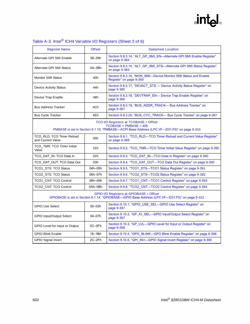
602 Intel® 82801DBM ICH4-M Datasheet
Register Index
Alternate GPI SMI Enable 38�39h Section 9.8.3.14, �ALT_GP_SMI_EN�Alternate GPI SMI Enable Register� on page 9-384
Alternate GPI SMI Status 3A�3Bh Section 9.8.3.15, �ALT_GP_SMI_STS�Alternate GPI SMI Status Register� on page 9-384
Monitor SMI Status 40h Section 9.8.3.16, �MON_SMI�Device Monitor SMI Status and Enable Register� on page 9-384
Device Activity Status 44h Section 9.8.3.17, �DEVACT_STS � Device Activity Status Register� on page 9-385
Device Trap Enable 48h Section 9.8.3.18, �DEVTRAP_EN� Device Trap Enable Register� on page 9-386
Bus Address Tracker 4Ch Section 9.8.3.19, �BUS_ADDR_TRACK� Bus Address Tracker� on page 9-387
Bus Cycle Tracker 4Eh Section 9.8.3.20, �BUS_CYC_TRACK� Bus Cycle Tracker� on page 9-387
TCO I/O Registers at TCOBASE + OffsetTCOBASE = PMBASE + 40h
PMBASE is set in Section 9.1.10, �PMBASE�ACPI Base Address (LPC I/F�D31:F0)� on page 9-310
TCO_RLD: TCO Timer Reload and Current Value 00h Section 9.9.1, �TCO_RLD�TCO Timer Reload and Current Value Register�
on page 9-389
TCO_TMR: TCO Timer Initial Value 01h Section 9.9.2, �TCO_TMR�TCO Timer Initial Value Register� on page 9-390
TCO_DAT_IN: TCO Data In 02h Section 9.9.3, �TCO_DAT_IN�TCO Data In Register� on page 9-390
TCO_DAT_OUT: TCO Data Out 03h Section 9.9.4, �TCO_DAT_OUT�TCO Data Out Register� on page 9-390
TCO1_STS: TCO Status 04h�05h Section 9.9.5, �TCO1_STS�TCO1 Status Register� on page 9-391
TCO2_STS: TCO Status 06h�07h Section 9.9.6, �TCO2_STS�TCO2 Status Register� on page 9-392
TCO1_CNT: TCO Control 08h�09h Section 9.9.7, �TCO1_CNT�TCO1 Control Register� on page 9-393
TCO2_CNT: TCO Control 0Ah�0Bh Section 9.9.8, �TCO2_CNT�TCO2 Control Register� on page 9-394
GPIO I/O Registers at GPIOBASE + OffsetGPIOBASE is set in Section 9.1.14, �GPIOBASE�GPIO Base Address (LPC I/F�D31:F0)� on page 9-312
GPIO Use Select 00�03h Section 9.10.1, �GPIO_USE_SEL�GPIO Use Select Register� on page 9-397
GPIO Input/Output Select 04�07h Section 9.10.2, �GP_IO_SEL�GPIO Input/Output Select Register� on page 9-397
GPIO Level for Input or Output 0C�0Fh Section 9.10.3, �GP_LVL�GPIO Level for Input or Output Register� on page 9-398
GPIO Blink Enable 18�1Bh Section 9.10.4, �GPO_BLINK�GPO Blink Enable Register� on page 9-398
GPIO Signal Invert 2C�2Fh Section 9.10.5, �GPI_INV�GPIO Signal Invert Register� on page 9-399
Table A-3. Intel® ICH4 Variable I/O Registers (Sheet 2 of 6)
Register Name Offset Datasheet Location

Intel® 82801DBM ICH4-M Datasheet 603
Register Index
BMIDE I/O Registers at BM_BASE + OffsetBM_BASE is set at Section 10.1.12, �SCMD_BAR�Secondary Command Block Base Address Register (IDE D31:F1)� on
page 10-406
Command Register Primary 00h Section 10.2.1, �BMIC[P,S]�Bus Master IDE Command Register� on page 10-415
Status Register Primary 02h Section 10.2.2, �BMIS[P,S]�Bus Master IDE Status Register� on page 10-416
Descriptor Table Pointer Primary 04�07h Section 10.2.3, �BMID[P,S]�Bus Master IDE Descriptor Table Pointer Register� on page 10-417
Command Register Secondary 08h Section 10.2.1, �BMIC[P,S]�Bus Master IDE Command Register� on page 10-415
Status Register Secondary 0Ah Section 10.2.2, �BMIS[P,S]�Bus Master IDE Status Register� on page 10-416
Descriptor Table Pointer Secondary 0C�0Fh Section 10.2.3, �BMID[P,S]�Bus Master IDE Descriptor Table Pointer
Register� on page 10-417
USB I/O Registers at Base Address + OffsetUSB Base Address is set at Section 11.1.10, �BASE�Base Address Register (USB�D29:F0/F1/F2)� on page 11-423
USB Command Register 00�01h Section 11.2.1, �USBCMD�USB Command Register� on page 11-428
USB Status Register 02�03h Section 11.2.2, �USBSTS�USB Status Register� on page 11-431
USB Interrupt Enable 04�05h Section 11.2.3, �USBINTR�Interrupt Enable Register� on page 11-432
USB Frame Number 06�07h Section 11.2.4, �FRNUM�Frame Number Register� on page 11-432
USB Frame List Base Address 08�0Bh Section 11.2.5, �FRBASEADD�Frame List Base Address� on page 11-433
USB Start of Frame Modify 0Ch Section 11.2.6, �SOFMOD�Start of Frame Modify Register� on page 11-434
Port 0, 2, 4 Status/Control 10�11h Section 11.2.7, �PORTSC[0,1]�Port Status and Control Register� on page 11-435
Port 1, 3, 5 Status/Control 12�13h Section 11.2.7, �PORTSC[0,1]�Port Status and Control Register� on page 11-435
SMBus I/O Registers at SMB_BASE + OffsetSMB_BASE is set at Section 13.1.8, �SMB_BASE�SMBUS Base Address Register (SMBUS�D31:F3)� on page 13-476
Host Status 00h Section 13.2.1, �HST_STS�Host Status Register� on page 13-478
Host Control 02h Section 13.2.2, �HST_CNT�Host Control Register� on page 13-480
Host Command 03h Section 13.2.3, �HST_CMD�Host Command Register� on page 13-481
Transmit Slave Address 04h Section 13.2.4, �XMIT_SLVA�Transmit Slave Address Register� on page 13-481
Host Data 0 05h Section 13.2.5, �HST_D0�Data 0 Register� on page 13-481
Host Data 1 06h Section 13.2.6, �HST_D1�Data 1 Register� on page 13-482
Block Data Byte 07h Section 13.2.7, �Host_BLOCK_DB�Host Block Data Byte Register� on page 13-482
Packet Error Check 08h Section 13.2.8, �PEC�Packet Error Check (PEC) Register� on page 13-482
Receive Slave Address 09h Section 13.2.9, �RCV_SLVA�Receive Slave Address Register� on page 13-483
Receive Slave Data 0Ah Section 13.2.10, �SLV_DATA�Receive Slave Data Register� on page 13-483
Table A-3. Intel® ICH4 Variable I/O Registers (Sheet 3 of 6)
Register Name Offset Datasheet Location

604 Intel® 82801DBM ICH4-M Datasheet
Register Index
Auxiliary Status 0Ch Section 13.2.11, �AUX_STS�Auxiliary Status Register� on page 13-483
Auxiliary Control 0Dh Section 13.2.12, �AUX_CTL�Auxiliary Control Register� on page 13-484
AC�97 Audio I/O Registers at NAMBAR + OffsetNAMBAR is set at Section 14.1.11, �NABMBAR�Native Audio Bus Mastering Base Address Register (Audio�D31:F5)�
on page 14-495
PCM In Buffer Descriptor list Base Address Register 00h Section 14.2.1, �x_BDBAR�Buffer Descriptor Base Address Register� on
page 14-504
PCM In Current Index Value 04h Section 14.2.2, �x_CIV�Current Index Value Register� on page 14-505
PCM In Last Valid Index 05h Section 14.2.3, �x_LVI�Last Valid Index Register� on page 14-505
PCM In Status Register 06h Section 14.2.4, �x_SR�Status Register� on page 14-506
PCM In Position In Current Buffer 08h Section 14.2.5, �x_PICB�Position In Current Buffer Register� on page 14-507
PCM In Prefetched Index Value 0Ah Section 14.2.6, �x_PIV�Prefetched Index Value Register� on page 14-507
PCM In Control Register 0Bh Section 14.2.7, �x_CR�Control Register� on page 14-508
PCM Out Buffer Descriptor list Base Address Register 10h Section 14.2.1, �x_BDBAR�Buffer Descriptor Base Address Register� on
page 14-504
PCM Out Current Index Value 14h Section 14.2.2, �x_CIV�Current Index Value Register� on page 14-505
PCM Out Last Valid Index 15h Section 14.2.3, �x_LVI�Last Valid Index Register� on page 14-505
PCM Out Status Register 16h Section 14.2.4, �x_SR�Status Register� on page 14-506
PCM Out Position In Current Buffer 18h Section 14.2.5, �x_PICB�Position In Current Buffer Register� on
page 14-507
PCM Out Prefetched Index Value 1Ah Section 14.2.6, �x_PIV�Prefetched Index Value Register� on page 14-507
PCM Out Control Register 1Bh Section 14.2.7, �x_CR�Control Register� on page 14-508
Mic. In Buffer Descriptor list Base Address Register 20h Section 14.2.1, �x_BDBAR�Buffer Descriptor Base Address Register� on
page 14-504
Mic. In Current Index Value 24h Section 14.2.2, �x_CIV�Current Index Value Register� on page 14-505
Mic. In Last Valid Index 25h Section 14.2.3, �x_LVI�Last Valid Index Register� on page 14-505
Mic. In Status Register 26h Section 14.2.4, �x_SR�Status Register� on page 14-506
Mic In Position In Current Buffer 28h Section 14.2.5, �x_PICB�Position In Current Buffer Register� on page 14-507
Mic. In Prefetched Index Value 2Ah Section 14.2.6, �x_PIV�Prefetched Index Value Register� on page 14-507
Mic. In Control Register 2Bh Section 14.2.7, �x_CR�Control Register� on page 14-508
Global Control 2Ch Section 14.2.8, �GLOB_CNT�Global Control Register� on page 14-509
Global Status 30h Section 14.2.9, �GLOB_STA�Global Status Register� on page 14-510
Codec Access Semaphore Register 34h Section 14.2.10, �CAS�Codec Access Semaphore Register� on
page 14-512
AC�97 Audio I/O Registers at MBBAR + OffsetMBBAR is set at Section 14.1.13, �MBBAR�Bus Master Base Address Register (Audio�D31:F5)� on page 14-496
Mic. 2 Buffer Descriptor list Base Address Register 40�43h Section 14.2.1, �x_BDBAR�Buffer Descriptor Base Address Register� on
page 14-504
Mic. 2 Current Index Value 44h Section 14.2.2, �x_CIV�Current Index Value Register� on page 14-505
Table A-3. Intel® ICH4 Variable I/O Registers (Sheet 4 of 6)
Register Name Offset Datasheet Location

Intel® 82801DBM ICH4-M Datasheet 605
Register Index
Mic. 2 Last Valid Index 45h Section 14.2.3, �x_LVI�Last Valid Index Register� on page 14-505
Mic. 2 Status Register 46�47h Section 14.2.4, �x_SR�Status Register� on page 14-506
Mic 2 Position In Current Buffer 48�49h Section 14.2.5, �x_PICB�Position In Current Buffer Register� on page 14-507
Mic. 2 Prefetched Index Value 4Ah Section 14.2.6, �x_PIV�Prefetched Index Value Register� on page 14-507
Mic. 2 Control Register 4Bh Section 14.2.7, �x_CR�Control Register� on page 14-508
PCM In 2 Buffer Descriptor list Base Address Register 50�53h Section 14.2.1, �x_BDBAR�Buffer Descriptor Base Address Register� on
page 14-504
PCM In 2 Current Index Value 54h Section 14.2.2, �x_CIV�Current Index Value Register� on page 14-505
PCM In 2 Last Valid Index 55h Section 14.2.3, �x_LVI�Last Valid Index Register� on page 14-505
PCM In 2 Status Register 56�57h Section 14.2.4, �x_SR�Status Register� on page 14-506
PCM In 2 Position In Current Buffer 58�59h Section 14.2.5, �x_PICB�Position In Current Buffer Register� on
page 14-507
PCM In 2 Prefetched Index Value 5Ah Section 14.2.6, �x_PIV�Prefetched Index Value Register� on page 14-507
PCM In 2 Control Register 5Bh Section 14.2.7, �x_CR�Control Register� on page 14-508
S/PDIF Buffer Descriptor list Base Address Register 60�63 Section 14.2.1, �x_BDBAR�Buffer Descriptor Base Address Register� on
page 14-504
S/PDIF Current Index Value 64h Section 14.2.2, �x_CIV�Current Index Value Register� on page 14-505
S/PDIF Last Valid Index 65h Section 14.2.3, �x_LVI�Last Valid Index Register� on page 14-505
S/PDIF Status Register 66�67h Section 14.2.4, �x_SR�Status Register� on page 14-506
S/PDIF Position In Current Buffer 68�69h Section 14.2.5, �x_PICB�Position In Current Buffer Register� on page 14-507
S/PDIF Prefetched Index Value 6Ah Section 14.2.6, �x_PIV�Prefetched Index Value Register� on page 14-507
S/PDIF Control Register 6Bh Section 14.2.7, �x_CR�Control Register� on page 14-508
SDATA_IN Map Register 80 Section 14.2.11, �SDM�SDATA_IN Map Register� on page 14-513
AC�97 Modem I/O Registers at MBAR + OffsetMBAR is set in Section 15.1.11, �MBAR�Modem Base Address Register (Modem�D31:F6)� on page 15-519
Modem In Buffer Descriptor List Base Address Register 00h Section 15.2.1, �x_BDBAR�Buffer Descriptor List Base Address Register�
on page 15-525
Modem In Current Index Value Register 04h Section 15.2.2, �x_CIV�Current Index Value Register� on page 15-525
Modem In Last Valid Index Register 05h Section 15.2.3, �x_LVI�Last Valid Index Register� on page 15-525
Modem In Status Register 06h Section 15.2.4, �x_SR�Status Register� on page 15-526
Modem In Position In Current Buffer Register 08h Section 15.2.5, �x_PICB�Position in Current Buffer Register� on
page 15-527
Modem In Prefetch Index Value Register 0Ah Section 15.2.6, �x_PIV�Prefetch Index Value Register� on page 15-527
Modem In Control Register 0Bh Section 15.2.7, �x_CR�Control Register� on page 15-528
Modem Out Buffer Descriptor List Base Address Register 10h Section 15.2.1, �x_BDBAR�Buffer Descriptor List Base Address Register�
on page 15-525
Modem Out Current Index Value Register 14h Section 15.2.2, �x_CIV�Current Index Value Register� on page 15-525
Table A-3. Intel® ICH4 Variable I/O Registers (Sheet 5 of 6)
Register Name Offset Datasheet Location

606 Intel® 82801DBM ICH4-M Datasheet
Register Index
Modem Out Last Valid Register 15h Section 15.2.3, �x_LVI�Last Valid Index Register� on page 15-525
Modem Out Status Register 16h Section 15.2.4, �x_SR�Status Register� on page 15-526
Modem In Position In Current Buffer Register 18h Section 15.2.5, �x_PICB�Position in Current Buffer Register� on
page 15-527
Modem Out Prefetched Index Register 1Ah Section 15.2.6, �x_PIV�Prefetch Index Value Register� on page 15-527
Modem Out Control Register 1Bh Section 15.2.7, �x_CR�Control Register� on page 15-528
Global Control 3Ch Section 15.2.8, �GLOB_CNT�Global Control Register� on page 15-529
Global Status 40h Section 15.2.9, �GLOB_STA�Global Status Register� on page 15-530
Codec Access Semaphore Register 44h Section 15.2.10, �CAS�Codec Access Semaphore Register� on
page 15-532
Table A-3. Intel® ICH4 Variable I/O Registers (Sheet 6 of 6)
Register Name Offset Datasheet Location

Register Bit Index
Intel® 82801DBM ICH4-M Datasheet 607
B Register Bit Index
Numerics64_EN 36264-bit Addressing Capability 45566 MHz Capable 268, 292, 296, 403, 421, 440,
475, 494, 519AA20Gate Pass-Through Enable 426AC 531AC �97 Cold Reset# 512, 531AC_SDIN0 Codec Ready 513, 533AC_SDIN0 Resume Interrupt 513, 533AC_SDIN0 Resume Interrupt Enable 511, 531AC_SDIN1 Codec Ready 513, 533AC_SDIN1 Resume Interrupt 513, 533AC_SDIN1 Resume Interrupt Enable 511, 531AC_SDIN2 Codec Ready 512, 532AC_SDIN2 Interrupt Enable 511, 531AC_SDIN2 Resume Interrupt 512, 532AC�97 Warm Reset 512, 531AC97_EN 379AC97_STS 378ACLINK Shut Off 511, 531AD3 513, 532ADDRESS 482Address Increment/Decrement Select 334Address of Descriptor Table 417ADLIB_ACT_STS 385ADLIB_LPC_EN 324ADLIB_TRP_EN 386AFTERG3_EN 364Alarm Flag 357Alarm Interrupt Enable 356Alternate A20 Gate 359Alternate Access Mode Enable 317Alternate GPI SMI Enable 384Alternate GPI SMI Status 384APIC Data 348APIC Enable 317APIC ID 349APIC Index 348APM_STS 383APMC_EN 381Arbiter Disable 376Asynchronous Schedule Enable 457Asynchronous Schedule Park Capability 455Asynchronous Schedule Status 459
AUDIO_ACT_STS 385AUDIO_TRP_EN 386Autoinitialize Enable 334Automatic End of Interrupt 342Automatically Append CRC 485Auxiliary Current 274, 444, 501BBAR Number 446Base Address 270, 271, 405, 406, 423, 433,
476, 496, 497, 498, 521Base and Current Address 331Base and Current Count 331Base Class Code 269, 404, 422, 476, 495, 520BATLOW_STS 377Binary/BCD Countdown Select 336BIOS_EN 381BIOS_STS 383BIOSWR_STS 391Bit 1 of slot 12 513, 533Bit 2 of slot 12 513, 533Bit 3 of slot 12 513, 533Bit Clock Stopped 512, 532Block Data 483BOOT_STS 392Buffer Completion Interrupt Status 508, 528Buffer Descriptor Base Address 506Buffer Descriptor List Base Address 527Buffered Mode 342Bus Master Enable 267, 402, 420, 439, 475,
493, 518Bus Master IDE Active 416Bus Master Reload 373Bus Master Status 371BUS_ERR 480Byte Done Status 479CCache Line Size 269Capabilities 499Capabilities List 268, 440, 494, 519Capabilities Pointer 272, 443, 499, 522Capability ID 273, 448, 501Cascaded Interrupt Controller IRQ Connection
341Channel 1 Select 315Channel 2 Select 315Channel 3 Select 315

Register Bit Index
608 Intel® 82801DBM ICH4-M Datasheet
Channel 5 Select 315Channel 6 Select 315Channel 7 Select 315Channel Mask Bits 335Channel Mask Select 333Channel Request Status 333Channel Terminal Count Status 333Clear Byte Pointer 334Clear Mask Register 335CNA Mask 278CNF1_LPC_EN 323CNF2_LPC_EN 323Codec Access Semaphore 514, 534COMA Decode Range 320COMA_LPC_EN 324COMB Decode Range 320COMB_LPC_EN 324Command Unit (CU) Executed 276Command Unit Command 279Command Unit Status 277Configure Flag 428Connect Status Change 436, 467COPROC_ERR 359Coprocessor Error Enable 316Count Register Status 338Countdown Type Status 338Counter 0 Select 337Counter 1 Select 337Counter 2 Select 337Counter Latch Command 337Counter Mode Selection 336Counter OUT Pin State 338Counter Port 338Counter Select 336Counter Selection 337CPU BIST Enable 319CPU Break Event Indication Enable 316CPU Frequency Strap 319CPU PLL Lock Time 363CPU Power Failure 363CPU SLP# Enable 362CPU Thermal Trip Status 363CRC Error 484CU Not Active 276Current Connect Status 436, 467Current Equals Last Valid 508, 528Current Index Value 507, 527CX Mask 278DD1 Support 274, 444D2 Support 274, 444
D29_F0_Disable 328D29_F1_Disable 328D29_F2_Disable 328D29_F7_Disable 328D31_F1_Disable 329D31_F3_Disable 329D31_F5_Disable 328D31_F6_Disable 328Data 282Data Message Byte 0 484Data Message Byte 1 484Data Mode 356Data Parity Error Detected 268, 403, 421, 475,
494, 519Data Scale 274, 445Data Select 274, 445DATA_BUFFER 470DATA_HIGH_BYTE 488DATA_LEN_CNT 469DATA_LOW_BYTE 488DATA0/COUNT 482DATA1 483Date Alarm 357Daylight Savings Enable 356Debug Port Number 454Debug Port Offset 446Deep Power-Down on Link Down Enable 286Delayed Transaction Enable 317Delivery Mode 352Delivery Status 351Delivery Type 350Destination 351Destination Mode 352Detected Parity Error 268, 403, 440, 475, 494,
519DEV_ERR 480DEV_TRAP_EN 384DEV_TRAP_STS 384Device Connects 218Device Identification Value 266, 290, 402, 420,
438, 474, 492, 518Device Monitor Status 382Device Specific Initialization 274, 501DEVICE_ADDRESS 487DEVSEL# Timing Status 268, 403, 421, 440,
475, 494, 519Diagnose Result 281Division Chain Select 355DMA Channel Group Enable 332DMA Channel Select 333, 334DMA Collection Buffer Enable 317

Register Bit Index
Intel® 82801DBM ICH4-M Datasheet 609
DMA Controller Halted 508, 528DMA Group Arbitration Priority 332DMA Low Page 332DMA Transfer Mode 334DMA Transfer Type 334DONE_STS 469Drive 0 DMA Capable 416Drive 0 DMA Timing Enable 409Drive 0 Fast Timing Bank 409Drive 0 IORDY Sample Point Enable 409Drive 0 Prefetch/Posting Enable 409Drive 1 DMA Capable 416Drive 1 DMA Timing Enable 409Drive 1 Fast Timing Bank 409Drive 1 IORDY Sample Point Enable 409Drive 1 Prefetch/Posting Enable 409Drive 1 Timing Register Enable 408DSI 444Duplex Mode 286Dynamic Data 274EEarly Receive 277Early Receive Count 283Edge/Level Bank Select 340EEPROM Chip Select 281EEPROM Serial Clock 281EEPROM Serial Data In 281EEPROM Serial Data Out 281EHC Initialization 209EHC Resets 210EHCI Extended Capabilities Pointer 455Enable 32-byte Buffer 485Enable Special Mask Mode 344ENABLED_CNT 469End of SMI 381Enter C4 When C3 Invoked 362Enter Global Suspend Mode 428ER Mask 278Error 416ERROR_GOOD#_STS 469EXCEPTION_STS 469Extended Destination ID 351FFAILED 480Fast Back to Back Capable 268, 292, 296, 403,
421, 440, 475, 494, 519Fast Back to Back Enable 267, 291, 402, 420,
439, 475, 493, 518Fast Primary Drive 0 Base Clock 413Fast Primary Drive 1 Base Clock 413Fast Secondary Drive 0 Base Clock 413
Fast Secondary Drive 1 Base Clock 413FC Full 284FC Paused 284FC Paused Low 284FCP Mask 278FDD Decode Range 321FDD_LPC_EN 324FIFO Error 508, 528FIFO Error Interrupt Enable 510, 530Flow Control Pause 277Flow Control Threshold 284Force Global Resume 428Force Port Resume 467Force Thermal Throttling 374FR Mask 278Frame Length Timing Value 447Frame List Current Index/Frame Number 432,
462Frame List Rollover 460Frame List Rollover Enable 461Frame List Size 457Frame Received 276Full Reset 360FWH_C0_EN 322, 327FWH_C0_IDSEL 325FWH_C8_EN 322, 327FWH_C8_IDSEL 325FWH_D0_EN 322, 327FWH_D0_IDSEL 325FWH_D8_EN 322, 327FWH_D8_IDSEL 325, 326FWH_E0_EN 322FWH_E0_IDSEL 325, 326FWH_E8_EN 322FWH_E8_IDSEL 325, 326FWH_F0_EN 322FWH_F0_IDSEL 325, 326FWH_F8_EN 322FWH_F8_IDSEL 325GGAMEH_LPC_EN 323GAMEL_LPC_EN 323GBL_SMI_EN 381General Self-Test Result 281Generic Decode Range 1 Enable 323Generic I/O Decode Range 1 Base Address 323Generic I/O Decode Range 2 Base Address 326Generic I/O Decode Range 2 Enable 326Global Enable 372Global Release 373Global Reset 428

Register Bit Index
610 Intel® 82801DBM ICH4-M Datasheet
Global Standby Timer Status 377Global Standby Timer Tick Rate 362Global Standby Timer Timeout Count 362Global Status 371GO_CNT 469GP_BLINK(n) 398GP_INV(n) 399GP_IO_SEL2 400GP_LVL(n) 398GP_LVL2 400GPE0_STS 383GPI Interrupt Enable 512, 531GPI Status Change Interrupt 514, 533GPI0 Route 365GPI1 Route 365GPI15 Route 365GPI2 Route 365GPIn_EN 379GPIn_STS 377GPIO_SEL 397GPIO_USE_SEL 397GPIO_USE_SEL2 399GPIO11_ALERT_DISABLE 394HHC BIOS Owned Semaphore 448HC OS Owned Semaphore 448HCHalted 431, 459Header Type 270, 422, 496, 520Host Controller Process Error 431Host Controller Reset 429, 458Host System Error 431, 459Host System Error Enable. 461HOST_BUSY 480HOST_NOTIFY_INTREN 487HOST_NOTIFY_STS 486HOST_NOTIFY_WKEN 487Hour Format 356HUBNMI_STS 391HUBSCI_STS 391HUBSERR_STS 391HUBSMI_STS 391II/O (x) Extension Enable 317I/O APIC Identification 350I/O Space Enable 267, 403, 420, 439, 475, 493,
501, 518I/O Space Indicator 271, 476I2C 233, 234I2C_EN 478ICW/OCW Select 340ICW4 Write Required 340
IDE Decode Enable 408IDEP0_ACT_STS 386IDEP0_TRP_EN 387IDEP1_ACT_STS 386IDEP1_TRP_EN 386IDES0_ACT_STS 385IDES0_TRP_EN 386IDES1_ACT_STS 385IDES1_TRP_EN 386IN_USE_CNT 469INIT_NOW 359Intel SpeedStep Enable 362INTEL_USB2_EN 380INTEL_USB2_STS 382Intel® SpeedStep� technology State 388Interesting Packet 285Interrupt 416Interrupt Enable 282Interrupt Input Pin Polarity 351Interrupt Level Select 343Interrupt Line 272, 408, 424, 443, 477, 499, 523Interrupt Mask 278Interrupt on Async Advance 459Interrupt on Async Advance Doorbell 457Interrupt on Async Advance Enable 461Interrupt On Complete (IOC) Enable 432Interrupt On Completion Enable 510, 530Interrupt Pin 272, 408, 424, 443, 477, 500, 523Interrupt Request Flag 357Interrupt Request Level 341Interrupt Request Mask 342Interrupt Routing Enable 313Interrupt Threshold Control 457Interrupt Vector Base Address 341INTR 480INTRD_SEL 394INTREN 482Intruder Detect 392INUSE_STS 480IOCHK# NMI Enable 358IOCHK# NMI Source Status 358IORDY Sample Point 408IRQ Number 348IRQ Routing 313IRQ1_CAUSE 395IRQ10 ECL 346IRQ11 ECL 346IRQ12 ECL 346IRQ12_CAUSE 395IRQ14 ECL 346IRQ15 ECL 346

Register Bit Index
Intel® 82801DBM ICH4-M Datasheet 611
IRQ3 ECL 345IRQ4 ECL 345IRQ5 ECL 345IRQ6 ECL 345IRQ7 ECL 345IRQ9 ECL 346Isochronous Scheduling Threshold 455KKBC_ACT_STS 385KBC_LPC_EN 323KBC_TRP_EN 386Keyboard IRQ1 Latch Enable 316KILL 482LLAN Connect Address 282LAN Connect Register Address 282LAN Connect Software Reset 286Last Codec Read Data Input 515Last Valid Buffer Completion Interrupt 508,
528Last Valid Buffer Interrupt Enable 510, 530Last Valid Index 507, 527Latch Count of Selected Counters 337Latch Status of Selected Counters 337LEG_ACT_STS 385LEG_IO_TRP_EN 386LEGACY_USB_EN 381LEGACY_USB_STS 383LEGACY_USB2_EN 380LEGACY_USB2_STS 382Light Host Controller Reset 457Line Status 436, 466Link Pointer Low 464Link Status Change Indication 285Link Status Indication 286LINK_ID_STS 469Loop Back Test Mode 428Low Speed Device Attached 435Lower 128-byte Lock 320LPC Bridge Disable 328LPT Decode Range 321LPT_LPC_EN 324MMagic Packet 285Management Data Interrupt 277Mask 351Master Abort Status 268, 494, 519Master Clear 335Master Data Parity Error Detected 440Master Latency Timer Count 270, 405Master/Slave in Buffered Mode 342
Max Packet 428Maximum Latency 273Maximum Redirection Entries 350MC_LPC_EN 323MD3 513, 532Memory Space Enable 267, 402, 420, 439, 475,
493, 518Memory Space Indicator 270Memory Write and Invalidate Enable 267, 291,
493, 518Mic In Interrupt 514, 533Microcontroller SMI Enable 380Microcontroller SMI# Status 383Microphone 2 In Interrupt 513, 532Microprocessor Mode 342MIDI Decode Range 321MIDI_ACT_STS 385MIDI_LPC_EN 324MIDI_TRP_EN 386Minimum Grant 272Mobile IDE Configuration Lock Down 317Mode Selection Status 338Modem In Interrupt 514, 533Modem Out Interrupt 514, 533MON_TRAP_BASE 367MON4_FWD_EN 366MON4_MASK 367MON5_FWD_EN 366MON5_MASK 367MON6_FWD_EN 366MON6_MASK 367MON7_FWD_EN 366MON7_MASK 367Mouse IRQ12 Latch Enable 316MSS Decode Range 321MSS_LPC_EN 324Multichannel Capabilities 513, 532Multi-Function Bit 422Multi-Function Device 270NN_PORTS 454NEWCENTURY_STS 391Next Capability 501Next EHCI Capability Pointer 448Next Item Pointer 273Next Item Pointer #1 Value 444NMI Enable 359NMI_NOW 393NMI2SMI_EN 392, 393NO_REBOOT 318Number of Companion Controllers 454

Register Bit Index
612 Intel® 82801DBM ICH4-M Datasheet
Number of Ports per Companion Controller 454OOCW2 Select 343OCW3 Select 344Opcode 282Over-current Active 435, 467Over-current Change 467Over-current Indicator 435OWNER_CNT 468PParity Error Response 267, 402, 420, 439, 475,
493, 518Pass Through State 426PCI CLKRUN# Enable 362PCI Interrupt Enable 425PCI SERR# Enable 358PCM 4/6 Enable 511PCM In 1, Microphone In 1 Data In Line 515PCM In 2 Interrupt 512, 532PCM In 2, Microphone In 2 Data In Line 515PCM In Interrupt 514, 533PCM Out Interrupt 514, 533PCM Out Mode 511PEC_DATA 483PEC_EN 481Periodic Interrupt Enable 356Periodic Interrupt Flag 357Periodic List Execution 211Periodic Schedule Enable 457Periodic Schedule Status 459Periodic SMI# Rate Select 362PERIODIC_EN 380PERIODIC_STS 382PIRQAE_ACT_STS 385PIRQBF_ACT_STS 385PIRQCG_ACT_STS 385PIRQDH_ACT_STS 385PM1_STS_REG 383PME Clock 274, 444, 501PME Enable 274, 445, 502, 524PME Status 274, 285, 445, 502, 524PME Support 274, 444, 501PME_B0_EN 379PME_B0_STS 377PME_EN 379PME_STS 377Pointer Field 280Poll Mode Command 344POP_MODE_CAP 404POP_MODE_SEL 404Port Change Detect 460
Port Change Interrupt Enable 461Port Enable/Disable Change 436, 467Port Enabled/Disabled 436, 467PORT Function Selection 280Port Owner 466Port Power 466Port Reset 435, 466Port Test Control 465Port Wake Implemented 447Port Wake Up Capability Mask 447PORT0EN 427PORT1EN 427Port-Routing Logic 217Position In Current Buffer 509, 529Positive Decode Enable 317Postable Memory Write Enable 402, 420, 439,
475Power Button Enable 372Power Button Override Status 370Power Button Status 371Power Failure 364Power Management Capability ID 443Power Sequencing 564Power State 275, 445, 502, 524Prefetchable 270, 442Prefetched Index Value 509, 529PRIM_SIG_MODE 413Primary Drive 0 Base Clock 414Primary Drive 0 Cycle Time 412Primary Drive 0 Synchronous DMA Mode En-
able 411Primary Drive 1 Base Clock 414Primary Drive 1 Cycle Time 412Primary Drive 1 IORDY Sample Point 410Primary Drive 1 Recovery Time 410Primary Drive 1 Synchronous DMA Mode En-
able 411Primary Master Channel Cable Reporting 414Primary Reset State 319Primary Slave Channel Cable Reporting 413Programmable Frame List Flag 455Programming Interface 421, 495, 519PRQ 350PWRBTN_LVL 362PWROK Failure 363RRate Select 355Read / Write Control 415Read Back Command 337Read Completion Status 513, 533Read Policies for Periodic DMA 211

Register Bit Index
Intel® 82801DBM ICH4-M Datasheet 613
Read/Write Select 336Read/Write Selection Status 338Ready 282Real Time Clock Index Address 359Receive DMA Byte Count 283Receive Not Ready 277Receive Unit Command 279Receive Unit Status 277Received 440Received Master Abort 403, 421, 440, 475Received Target Abort 268, 440, 475RECEIVED_PID_STS 470Reclamation 459Recovery Time 409Redirection Entry Clear 349Refresh Cycle Toggle 358Register Read Command 344Register Result 281Remote IRR 351Reset CPU 360Reset Registers 510, 530Resource Type Indicator 405, 406, 423, 442,
496, 497, 498, 521Resume Detect 431, 435Resume Interrupt Enable 432Revision Identification Value 269, 403, 421,
476, 495, 519RI_EN 379RI_STS 377RNR Mask 278ROM Content Result 281Rotate and EOI Codes 343RTC Event Enable 372RTC Power Status 364RTC Status 370Run/Pause Bus Master 510, 530Run/Stop 429, 458RW 482SS/PDIF Interrupt 512, 532S/PDIF Slot Map 511SAFE_MODE 318Sample Capabilities 513, 532SB16 Decode Range 321SB16_LPC_EN 324SCB General Pointer 280SCI Enable 373SEC_SIG_MODE 413SECOND_TO_STS 392Secondary Codec ID 500Secondary Drive 0 Base Clock 414
Secondary Drive 0 Cycle Time 412Secondary Drive 0 Synchronous DMA Mode
Enable 411Secondary Drive 1 Base Clock 414Secondary Drive 1 Cycle Time 412Secondary Drive 1 IORDY Sample Point 410Secondary Drive 1 Recovery Time 410Secondary Drive 1 Synchronous DMA Mode
Enable 411Secondary Master Channel Cable Reporting
413Secondary Reset State 319Secondary Slave Channel Cable Reporting 413SEND_PID_CNT 470SENDNOW 393SERIRQ_SMI_STS 382SERR# Enable 267, 402, 420, 439, 475, 493,
518SERR# NMI Source Status 358Short Packet Interrupt Enable 432Signaled System Error 268, 403, 440, 475, 494,
519Signaled Target Abort 268, 403, 421, 440, 475,
494, 519Single or Cascade 340Slave Identification Code 342SLAVE_ADDR 484Sleep Enable 373Sleep Type 373SLP_SMI_EN 381SLP_SMI_STS 383SMB_CMD 481SMB_FOR_BIOS 329SMB_SMI_EN 478SMBALERT_DIS 487SMBALERT_STS 480SMBCLK_CTL 486SMBCLK_CUR_STS 486SMBDATA_CUR_STS 486SMBus Host Enable 478SMBus SMI Status 382SMBus Wake Status 378SMI at End of Pass-through Enable 426SMI Caused by End of Pass-through 425SMI Caused by Port 60 Read 426SMI Caused by Port 60 Write 425SMI Caused by Port 64 Read 425SMI Caused by Port 64 Write 425SMI Caused by USB Interrupt 425SMI on Async 451SMI on Async Advance 449

Register Bit Index
614 Intel® 82801DBM ICH4-M Datasheet
SMI on Async Advance Enable 450SMI on Async Enable 451SMI on BAR 449SMI on BAR Enable 449SMI on CF 451SMI on CF Enable 452SMI on Frame List Rollover 449SMI on Frame List Rollover Enable 450SMI on HCHalted 451SMI on HCHalted Enable 452SMI on HCReset 451SMI on HCReset Enable 452SMI on Host System Error 449SMI on Host System Error Enable 450SMI on OS Ownership Change 449SMI on OS Ownership Enable 449SMI on PCI Command 449SMI on PCI Command Enable 449SMI on Periodic 451SMI on Periodic Enable 451SMI on PMCSR 451SMI on PMSCR Enable 451SMI on Port 60 Reads Enable 426SMI on Port 60 Writes Enable 426SMI on Port 64 Reads Enable 426SMI on Port 64 Writes Enable 426SMI on Port Change Detect 449SMI on Port Change Enable 450SMI on PortOwner 451SMI on PortOwner Enable 451SMI on USB Complete 449SMI on USB Complete Enable 450SMI on USB Error 449SMI on USB Error Enable 450SMI on USB IRQ Enable 426SMI_LOCK 362SMLink Slave SMI Status 392SMLINK_CLK_CTL 485SMLINK0_CUR_STS 485SMLINK1_CUR_STS 485SOF Timing Value 434Software Debug 428Software Generated Interrupt 278Software Interrupt 277Software SMI# Timer Enable 381SOP_MODE_CAP 404SOP_MODE_SEL 404Speaker Data Enable 358Special Cycle Enable 267, 291, 402, 420, 439,
475, 493, 518Special Fully Nested Mode 342
Special Mask Mode 344Speed 286Square Wave Enable 356START 481Start/Stop Bus Master 415Steer Enable 515STPCLK_DE 365Sub Class Code 269, 404, 422, 476, 495, 520Subsystem ID 271, 407, 423, 477, 499, 522Subsystem Vendor ID 271, 407, 423, 477, 498,
522Suspend 435, 466SW_TCO_SMI 392SWSMI_RATE_SEL 364SWSMI_TMR_STS 383System Reset 360System Reset Status 363TTCO Timer Halt 393TCO_EN 380TCO_INT_STS 392TCO_MESSAGE 394TCO_STS 382TCOSCI_EN 379TCOSCI_STS 378Tertiary Codec ID 500Thermal Interrupt Override Status 378Thermal Interrupt Status 378THRM#_POL 380THRM_DTY 374THRM_EN 380Throttle Status 374THT_EN 375THTL_DTY 375TIMEOUT 391Timeout/CRC Interrupt Enable 432Timer Counter 2 Enable 358Timer Counter 2 OUT Status 358Timer Overflow Interrupt Enable 372Timer Overflow Status 371Timer Value 374TOKEN_PID_CNT 470Top-Block Swap Mode 319Trigger Mode 351Type 270, 442, 497, 498UUpdate Cycle Inhibit 356Update In Progress 355Update-ended Flag 357Update-Ended Interrupt Enable 356Upper 128-byte Enable 320

Register Bit Index
Intel® 82801DBM ICH4-M Datasheet 615
Upper 128-byte Lock 320USB Error Interrupt 431, 460USB Error Interrupt Enable 461USB HS Ref Voltage 452USB Interrupt 431, 460USB Interrupt Enable 461USB Release Number 424, 446USB UHCI Port Owner 448USB_ADDRESS_CNF 471USB_ENDPOINT_CNF 471USB1_EN 380USB1_STS 378USB2_EN 379USB2_STS 378USB3_EN 379USB3_STS 377User Definable Features 268, 292, 296, 403,
421, 440, 475, 494, 519VValid RAM and Time Bit 357
Vector 352Vendor Identification Value 266, 290, 402,
419, 438, 473, 492, 518Version 274, 350, 444, 501VGA Palette Snoop 267, 291, 402, 420, 439,
475, 493, 518WWait Cycle Control 267, 291, 402, 420, 439,
475, 493, 518Wake Status 370Watchdog Status 395WR_PingPong_EN 413Write Policies for Periodic DMA 212WRITE_READ#_CNT 469WRT_RDONLY 452XXoff 284Xon 284


