Order Number: 306666, Revision: 001 April 2005 Intel StrataFlash ® Embedded Memory (P30) 1-Gbit P30 Family Datasheet Product Features The Intel StrataFlash ® Embedded Memory (P30) product is the latest generation of Intel StrataFlash ® memory devices. Offered in 64-Mbit up through 1-Gbit densities, the P30 device brings reliable, two-bit-per-cell storage technology to the embedded flash market segment. Benefits include more density in less space, high-speed interface, lowest cost-per-bit NOR device, and support for code and data storage. Features include high-performance synchronous- burst read mode, fast asynchronous access times, low power, flexible security options, and three industry standard package choices. The P30 product family is manufactured using Intel ® 130 nm ETOX™ VIII process technology. ■ High performance — 85/88 ns initial access — 40 MHz with zero wait states, 20 ns clock-to- data output synchronous-burst read mode — 25 ns asynchronous-page read mode — 4-, 8-, 16-, and continuous-word burst mode — Buffered Enhanced Factory Programming (BEFP) at 5 μs/byte (Typ) — 1.8 V buffered programming at 7 μs/byte (Typ) ■ Architecture — Multi-Level Cell Technology: Highest Density at Lowest Cost — Asymmetrically-blocked architecture — Four 32-KByte parameter blocks: top or bottom configuration — 128-KByte main blocks ■ Voltage and Power —V CC (core) voltage: 1.7 V – 2.0 V —V CCQ (I/O) voltage: 1.7 V – 3.6 V — Standby current: 55 μA (Typ) for 256-Mbit — 4-Word synchronous read current: 13 mA (Typ) at 40 MHz ■ Quality and Reliability — Operating temperature: –40 °C to +85 °C • 1-Gbit in SCSP is –30 °C to +85 °C — Minimum 100,000 erase cycles per block — ETOX™ VIII process technology (130 nm) ■ Security — One-Time Programmable Registers: • 64 unique factory device identifier bits • 64 user-programmable OTP bits • Additional 2048 user-programmable OTP bits — Selectable OTP Space in Main Array: • 4x32KB parameter blocks + 3x128KB main blocks (top or bottom configuration) — Absolute write protection: V PP = V SS — Power-transition erase/program lockout — Individual zero-latency block locking — Individual block lock-down ■ Software — 20 μs (Typ) program suspend — 20 μs (Typ) erase suspend — Intel ® Flash Data Integrator optimized — Basic Command Set and Extended Command Set compatible — Common Flash Interface capable ■ Density and Packaging — 64/128/256-Mbit densities in 56-Lead TSOP package — 64/128/256/512-Mbit densities in 64-Ball Intel® Easy BGA package — 64/128/256/512-Mbit and 1-Gbit densities in Intel® QUAD+ SCSP — 16-bit wide data bus
Transcript
Order Number: 306666, Revision: 001April 2005
Intel StrataFlash® Embedded Memory (P30)1-Gbit P30 Family
Datasheet
Product Features
The Intel StrataFlash® Embedded Memory (P30) product is the latest generation of Intel StrataFlash® memory devices. Offered in 64-Mbit up through 1-Gbit densities, the P30 device brings reliable, two-bit-per-cell storage technology to the embedded flash market segment. Benefits include more density in less space, high-speed interface, lowest cost-per-bit NOR device, and support for code and data storage. Features include high-performance synchronous-burst read mode, fast asynchronous access times, low power, flexible security options, and three industry standard package choices.
The P30 product family is manufactured using Intel® 130 nm ETOX™ VIII process technology.
■ High performance— 85/88 ns initial access— 40 MHz with zero wait states, 20 ns clock-to-
■ Software— 20 µs (Typ) program suspend— 20 µs (Typ) erase suspend— Intel® Flash Data Integrator optimized— Basic Command Set and Extended Command
Set compatible— Common Flash Interface capable
■ Density and Packaging— 64/128/256-Mbit densities in 56-Lead TSOP
package— 64/128/256/512-Mbit densities in 64-Ball
Intel® Easy BGA package— 64/128/256/512-Mbit and 1-Gbit densities in
Intel® QUAD+ SCSP— 16-bit wide data bus
April 2005 Intel StrataFlash® Embedded Memory (P30) Datasheet2 Order Number: 306666, Revision: 001
INFORMATION IN THIS DOCUMENT IS PROVIDED IN CONNECTION WITH INTEL PRODUCTS. NO LICENSE, EXPRESS OR IMPLIED, BY ESTOPPEL OR OTHERWISE, TO ANY INTELLECTUAL PROPERTY RIGHTS IS GRANTED BY THIS DOCUMENT. EXCEPT AS PROVIDED IN INTEL'S TERMS AND CONDITIONS OF SALE FOR SUCH PRODUCTS, INTEL ASSUMES NO LIABILITY WHATSOEVER, AND INTEL DISCLAIMS ANY EXPRESS OR IMPLIED WARRANTY, RELATING TO SALE AND/OR USE OF INTEL PRODUCTS INCLUDING LIABILITY OR WARRANTIES RELATING TO FITNESS FOR A PARTICULAR PURPOSE, MERCHANTABILITY, OR INFRINGEMENT OF ANY PATENT, COPYRIGHT OR OTHER INTELLECTUAL PROPERTY RIGHT. Intel products are not intended for use in medical, life saving, or life sustaining applications.
Intel may make changes to specifications and product descriptions at any time, without notice.
This document contains information on products in the design phase of development. The information here is subject to change without notice. Do not finalize a design with this information.
StrataFlash® Embedded Memory (P30) Contact your local Intel sales office or your distributor to obtain the latest specifications and before placing your product order.
Copies of documents which have an ordering number and are referenced in this document, or other Intel literature may be obtained by calling 1-800-548-4725 or by visiting Intel's website at http://www.intel.com.
4.0 Ballout and Signal Descriptions......................................................................................174.1 Signal Ballout......................................................................................................................174.2 Signal Descriptions .............................................................................................................204.3 SCSP Configurations..........................................................................................................224.4 Memory Maps .....................................................................................................................24
5.0 Maximum Ratings and Operating Conditions ...........................................................295.1 Absolute Maximum Ratings ................................................................................................295.2 Operating Conditions ..........................................................................................................30
6.0 Electrical Specifications .....................................................................................................316.1 DC Current Characteristics .................................................................................................316.2 DC Voltage Characteristics.................................................................................................32
7.0 AC Characteristics ................................................................................................................337.1 AC Test Conditions.............................................................................................................337.2 Capacitance........................................................................................................................347.3 AC Read Specifications ......................................................................................................357.4 AC Write Specifications ......................................................................................................417.5 Program and Erase Characteristics ....................................................................................45
8.0 Power and Reset Specifications .....................................................................................468.1 Power Up and Down...........................................................................................................468.2 Reset Specifications ...........................................................................................................468.3 Power Supply Decoupling...................................................................................................47
9.0 Device Operations.................................................................................................................489.1 Bus Operations ...................................................................................................................48
11.4 Program Suspend............................................................................................................... 6511.5 Program Resume................................................................................................................ 6611.6 Program Protection............................................................................................................. 66
13.3.1 Reading the Protection Registers .......................................................................... 7313.3.2 Programming the Protection Registers.................................................................. 7313.3.3 Locking the Protection Registers ........................................................................... 74
14.0 Special Read States ............................................................................................................. 7514.1 Read Status Register.......................................................................................................... 75
14.1.1 Clear Status Register............................................................................................. 7614.2 Read Device Identifier ........................................................................................................ 76
This document provides information about the Intel StrataFlash® Embedded Memory (P30) device and describes its features, operation, and specifications.
1.1 Nomenclature
1.2 Acronyms
1.8 V : VCC (core) voltage range of 1.7 V – 2.0 V
3.0 V : VCCQ (I/O) voltage range of 1.7 V – 3.6 V
9.0 V : VPP voltage range of 8.5 V – 9.5 V
Block : A group of bits, bytes,1-Gbit P30 Family or words within the flash memory array that erase simultaneously when the Erase command is issued to the device. The 1-Gbit P30 Family has two block sizes: 32-KByte and 128-KByte.
Main block : An array block that is usually used to store code and/or data. Main blocks are larger than parameter blocks.
Parameter block : An array block that is usually used to store frequently changing data or small system parameters that traditionally would be stored in EEPROM.
Top parameter device : A device with its parameter blocks located at the highest physical address of its memory map.
Bottom parameter device : A device with its parameter blocks located at the lowest physical address of its memory map.
BEFP : Buffer Enhanced Factory Programming
CUI : Command User Interface
MLC : Multi-Level Cell
OTP : One-Time Programmable
PLR : Protection Lock Register
PR : Protection Register
RCR : Read Configuration Register
1-Gbit P30 Family
April 2005 Intel StrataFlash® Embedded Memory (P30) Datasheet8 Order Number: 306666, Revision: 001
1.3 Conventions
RFU : Reserved for Future Use
SR : Status Register
WSM : Write State Machine
VCC : Signal or voltage connection
VCC : Signal or voltage level
0x : Hexadecimal number prefix
0b : Binary number prefix
SR[4] : Denotes an individual register bit.
A[15:0] : Denotes a group of similarly named signals, such as address or data bus.
A5 : Denotes one element of a signal group membership, such as an individual address bit.
This section provides an overview of the features and capabilities of the 1-Gbit P30 Family device.
The P30 family provides density upgrades from 64-Mbit through 1-Gbit. This family of devices provides high performance at low voltage on a 16-bit data bus. Individually erasable memory blocks are sized for optimum code and data storage.
Upon initial power up or return from reset, the device defaults to asynchronous page-mode read. Configuring the Read Configuration Register enables synchronous burst-mode reads. In synchronous burst mode, output data is synchronized with a user-supplied clock signal. A WAIT signal provides an easy CPU-to-flash memory synchronization.
In addition to the enhanced architecture and interface, the device incorporates technology that enables fast factory program and erase operations. Designed for low-voltage systems, the 1-Gbit P30 Family supports read operations with VCC at 1.8 V, and erase and program operations with VPP at 1.8 V or 9.0 V. Buffered Enhanced Factory Programming (BEFP) provides the fastest flash array programming performance with VPP at 9.0 V, which increases factory throughput. With VPPat 1.8 V, VCC and VPP can be tied together for a simple, ultra low power design. In addition to voltage flexibility, a dedicated VPP connection provides complete data protection when VPP ≤VPPLK.
A Command User Interface (CUI) is the interface between the system processor and all internal operations of the device. An internal Write State Machine (WSM) automatically executes the algorithms and timings necessary for block erase and program. A Status Register indicates erase or program completion and any errors that may have occurred.
An industry-standard command sequence invokes program and erase automation. Each erase operation erases one block. The Erase Suspend feature allows system software to pause an erase cycle to read or program data in another block. Program Suspend allows system software to pause programming to read other locations. Data is programmed in word increments (16 bits).
The 1-Gbit P30 Family’s protection register allows unique flash device identification that can be used to increase system security. The individual Block Lock feature provides zero-latency block locking and unlocking. In addition, the P30 device also has four pre-defined spaces in the main array that can be configured as One-Time Programmable (OTP).
1-Gbit P30 Family
April 2005 Intel StrataFlash® Embedded Memory (P30) Datasheet10 Order Number: 306666, Revision: 001
3.0 Package Information
3.1 56-Lead TSOP Package
Figure 1. TSOP Mechanical Specifications
A
0
L
Detail A
Y
D
C
Z
Pin 1
E
D1
b
Detail B
See Detail A
e
See Detail B
A1
SeatingPlane
A2See Note 2
[231369-90]
See Notes 1 and 3
Table 1. TSOP Package Dimensions (Sheet 1 of 2)
Product Information SymMillimeters Inches
Min Nom Max Min Nom Max
Package Height A - - 1.200 - - 0.047
Standoff A1 0.050 - - 0.002 - -
Package Body Thickness A2 0.965 0.995 1.025 0.038 0.039 0.040
Lead Width b 0.100 0.150 0.200 0.004 0.006 0.008
Lead Thickness c 0.100 0.150 0.200 0.004 0.006 0.008
Package Body Length D1 18.200 18.400 18.600 0.717 0.724 0.732
Package Body Width E 13.800 14.000 14.200 0.543 0.551 0.559
Millimeters InchesDimens ions Symbol Min Nom Max Min Nom MaxPackage Height A - - 1.400 - - 0.0551Ball Height A1 0.200 - - 0.0079 - -Package Body Thickness A2 - 1.070 - - 0.0421 -Ball (Lead) W idth b 0.325 0.375 0.425 0.0128 0.0148 0.0167Package Body Length D 10.900 11.000 11.100 0.4291 0.4331 0.4370Package Body W idth E 10.900 11.000 11.100 0.4291 0.4331 0.4370Pitch e - 0.800 - - 0.0315 -Ball (Lead) Count N - 88 - - 88 -Seating Plane Coplanarity Y - - 0.100 - - 0.0039Corner to Ball A1 Dis tance Along E S1 2.600 2.700 2.800 0.1024 0.1063 0.1102Corner to Ball A1 Dis tance Along D S2 1.000 1.100 1.200 0.0394 0.0433 0.0472
Notes:1. A1 is the least significant address bit.2. A23 is valid for 128-Mbit densities and above; otherwise, it is a no connect (NC).3. A24 is valid for 256-Mbit densities and above; otherwise, it is a no connect (NC).
Figure 7. 56-Lead TSOP Pinout (64/128/256-Mbit)
Intel StrataFlash® Embedded Memory (P30)
56-Lead TSOP Pinout14 mm x 20 mm
Top View
1
34
2
5
78
6
9
1112
10
13
1516
14
17
1920
18
21
2324
22
25
2728
26
56
5453
55
52
5049
51
48
4645
47
44
4241
43
40
3837
39
36
3433
35
32
3029
31
A14A13A12
A10A9
A11
A23
A21VSS
A22
VCC
WP#A20
WE#
A19
A8A7
A18
A6
A4A3
A5
A2
RFUVSS
A24
WAIT
DQ15DQ7
A17
DQ14
DQ13DQ5
DQ6
DQ12
ADV#CLK
DQ4
RST#
A16
DQ3
VPP
DQ10
VCCQDQ9
DQ2
DQ1
DQ0VCC
DQ8
OE#
CE#A1
VSS
A15
DQ11
1-Gbit P30 Family
April 2005 Intel StrataFlash® Embedded Memory (P30) Datasheet18 Order Number: 306666, Revision: 001
Notes:1. A1 is the least significant address bit.2. A23 is valid for 128-Mbit densities and above; otherwise, it is a no connect (NC).3. A24 is valid for 256-Mbit densities and above; otherwise, it is a no connect (NC).4. A25 is valid for 512-Mbit densities; otherwise, it is a no connect (NC).
April 2005 Intel StrataFlash® Embedded Memory (P30) Datasheet20 Order Number: 306666, Revision: 001
4.2 Signal Descriptions
This section has signal descriptions for the various P30 packages.
Table 3. TSOP and Easy BGA Signal Descriptions (Sheet 1 of 2)
Symbol Type Name and Function
A[MAX:1] InputADDRESS INPUTS: Device address inputs. 64-Mbit: A[22:1]; 128-Mbit: A[23:1]; 256-Mbit: A[24:1]; 512-Mbit: A[25:1].See Table 5 on page 22 and Figure 10 on page 23 for 512-Mbit addressing.
DQ[15:0] Input/Output
DATA INPUT/OUTPUTS: Inputs data and commands during write cycles; outputs data during memory, Status Register, Protection Register, and Read Configuration Register reads. Data balls float when the CE# or OE# are deasserted. Data is internally latched during writes.
ADV# Input
ADDRESS VALID: Active low input. During synchronous read operations, addresses are latched on the rising edge of ADV#, or on the next valid CLK edge with ADV# low, whichever occurs first. In asynchronous mode, the address is latched when ADV# going high or continuously flows through if ADV# is held low. WARNING: Designs not using ADV# must tie it to VSS to allow addresses to flow through.
CE# Input
FLASH CHIP ENABLE: Active low input. CE# low selects the associated flash memory die. When asserted, flash internal control logic, input buffers, decoders, and sense amplifiers are active. When deasserted, the associated flash die is deselected, power is reduced to standby levels, data and WAIT outputs are placed in high-Z state. WARNING: All chip enables must be high when device is not in use.
CLK Input
CLOCK: Synchronizes the device with the system’s bus frequency in synchronous-read mode. During synchronous read operations, addresses are latched on the rising edge of ADV#, or on the next valid CLK edge with ADV# low, whichever occurs first.WARNING: Designs not using CLK for synchronous read mode must tie it to VCCQ or VSS.
OE# Input OUTPUT ENABLE: Active low input. OE# low enables the device’s output data buffers during read cycles. OE# high places the data outputs and WAIT in High-Z.
RST# InputRESET: Active low input. RST# resets internal automation and inhibits write operations. This provides data protection during power transitions. RST# high enables normal operation. Exit from reset places the device in asynchronous read array mode.
WAIT Output
WAIT: Indicates data valid in synchronous array or non-array burst reads. Read Configuration Register bit 10 (RCR[10], WT) determines its polarity when asserted. WAIT’s active output is VOL or VOH when CE# and OE# are VIL. WAIT is high-Z if CE# or OE# is VIH.
• In synchronous array or non-array read modes, WAIT indicates invalid data when asserted and valid data when deasserted.
• In asynchronous page mode, and all write modes, WAIT is deasserted.
WE# Input WRITE ENABLE: Active low input. WE# controls writes to the device. Address and data are latched on the rising edge of WE#.
WP# InputWRITE PROTECT: Active low input. WP# low enables the lock-down mechanism. Blocks in lock-down cannot be unlocked with the Unlock command. WP# high overrides the lock-down function enabling blocks to be erased or programmed using software commands.
VPP Power/Input
Erase and Program Power: A valid voltage on this pin allows erasing or programming. Memory contents cannot be altered when VPP ≤ VPPLK. Block erase and program at invalid VPP voltages should not be attempted.Set VPP = VCC for in-system program and erase operations. To accommodate resistor or diode drops from the system supply, the VIH level of VPP can be as low as VPPL min. VPP must remain above VPPLmin to perform in-system flash modification. VPP may be 0 V during read operations.VPPH can be applied to main blocks for 1000 cycles maximum and to parameter blocks for 2500 cycles. VPP can be connected to 9 V for a cumulative total not to exceed 80 hours. Extended use of this pin at 9 V may reduce block cycling capability.
VCC Power Device Core Power Supply: Core (logic) source voltage. Writes to the flash array are inhibited when VCC ≤ VLKO. Operations at invalid VCC voltages should not be attempted.
VCCQ Power Output Power Supply: Output-driver source voltage.
VSS Power Ground: Connect to system ground. Do not float any VSS connection.
RFU — Reserved for Future Use: Reserved by Intel for future device functionality and enhancement. These should be treated in the same way as a Do Not Use (DU) signal.
DU — Do Not Use: Do not connect to any other signal, or power supply; must be left floating.
NC — No Connect: No internal connection; can be driven or floated.
Table 3. TSOP and Easy BGA Signal Descriptions (Sheet 2 of 2)
Symbol Type Name and Function
Table 4. QUAD+ SCSP Signal Descriptions (Sheet 1 of 2)
Symbol Type Name and Function
A[MAX:0] Input
ADDRESS INPUTS: Device address inputs. 64-Mbit: A[21:0]; 128-Mbit: A[22:0]; 256-Mbit: A[23:0]; 512-Mbit: A[24:0]. See Table 6 on page 22, Figure 11 on page 23, and Figure 12 on page 23 for 512-Mbit and 1-Gbit addressing.
DQ[15:0] Input/Output
DATA INPUT/OUTPUTS: Inputs data and commands during write cycles; outputs data during memory, Status Register, Protection Register, and Read Configuration Register reads. Data balls float when the CE# or OE# are deasserted. Data is internally latched during writes.
ADV# Input
ADDRESS VALID: Active low input. During synchronous read operations, addresses are latched on the rising edge of ADV#, or on the next valid CLK edge with ADV# low, whichever occurs first. In asynchronous mode, the address is latched when ADV# going high or continuously flows through if ADV# is held low. WARNING: Designs not using ADV# must tie it to VSS to allow addresses to flow through.
F1-CE#F2-CE#
Input
FLASH CHIP ENABLE: Active low input. CE# low selects the associated flash memory die. When asserted, flash internal control logic, input buffers, decoders, and sense amplifiers are active. When deasserted, the associated flash die is deselected, power is reduced to standby levels, data and WAIT outputs are placed in high-Z state. See Table 6 on page 22 for CE# assignment definitions.WARNING: All chip enables must be high when device is not in use.
CLK Input
CLOCK: Synchronizes the device with the system’s bus frequency in synchronous-read mode. During synchronous read operations, addresses are latched on the rising edge of ADV#, or on the next valid CLK edge with ADV# low, whichever occurs first.WARNING: Designs not using CLK for synchronous read mode must tie it to VCCQ or VSS.
F1-OE#F2-OE#
InputOUTPUT ENABLE: Active low input. OE# low enables the device’s output data buffers during read cycles. OE# high places the data outputs and WAIT in High-Z. F1-OE# and F2-OE# should be tied together for all densities.
RST# InputRESET: Active low input. RST# resets internal automation and inhibits write operations. This provides data protection during power transitions. RST# high enables normal operation. Exit from reset places the device in asynchronous read array mode.
WAIT Output
WAIT: Indicates data valid in synchronous array or non-array burst reads. Read Configuration Register bit 10 (RCR[10], WT) determines its polarity when asserted. WAIT’s active output is VOL or VOH when CE# and OE# are VIL. WAIT is high-Z if CE# or OE# is VIH.
• In synchronous array or non-array read modes, WAIT indicates invalid data when asserted and valid data when deasserted.
• In asynchronous page mode, and all write modes, WAIT is deasserted.
WE# Input WRITE ENABLE: Active low input. WE# controls writes to the device. Address and data are latched on the rising edge of WE#.
1-Gbit P30 Family
April 2005 Intel StrataFlash® Embedded Memory (P30) Datasheet22 Order Number: 306666, Revision: 001
4.3 SCSP Configurations
WP# InputWRITE PROTECT: Active low input. WP# low enables the lock-down mechanism. Blocks in lock-down cannot be unlocked with the Unlock command. WP# high overrides the lock-down function enabling blocks to be erased or programmed using software commands.
VPP Power/lnput
Erase and Program Power: A valid voltage on this pin allows erasing or programming. Memory contents cannot be altered when VPP ≤ VPPLK. Block erase and program at invalid VPP voltages should not be attempted.Set VPP = VCC for in-system program and erase operations. To accommodate resistor or diode drops from the system supply, the VIH level of VPP can be as low as VPPL min. VPP must remain above VPPLmin to perform in-system flash modification. VPP may be 0 V during read operations.VPPH can be applied to main blocks for 1000 cycles maximum and to parameter blocks for 2500 cycles. VPP can be connected to 9 V for a cumulative total not to exceed 80 hours. Extended use of this pin at 9 V may reduce block cycling capability.
VCC Power Device Core Power Supply: Core (logic) source voltage. Writes to the flash array are inhibited when VCC ≤ VLKO. Operations at invalid VCC voltages should not be attempted.
VCCQ Power Output Power Supply: Output-driver source voltage.
VSS Power Ground: Connect to system ground. Do not float any VSS connection.
RFU — Reserved for Future Use: Reserved by Intel for future device functionality and enhancement. These should be treated in the same way as a Do Not Use (DU) signal.
DU — Do Not Use: Do not connect to any other signal, or power supply; must be left floating.
NC — No Connect: No internal connection; can be driven or floated.
Table 4. QUAD+ SCSP Signal Descriptions (Sheet 2 of 2)
Warning: Stressing the device beyond the “Absolute Maximum Ratings” may cause permanent damage. These are stress ratings only.
Parameter Maximum Rating Notes
Temperature under bias –40 °C to +85 °C 1
Storage temperature –65 °C to +125 °C
Voltage on any signal (except VCC, VPP) –0.5 V to +4.1 V 2
VPP voltage –0.2 V to +10 V 2,3,4
VCC voltage –0.2 V to +2.5 V 2
VCCQ voltage –0.2 V to +4.1 V 2
Output short circuit current 100 mA 5
Notes:1. Temperature for 1-Gbit SCSP is –30 °C to +85 °C.2. Voltages shown are specified with respect to VSS. Minimum DC voltage is –0.5 V on input/output
signals and –0.2 V on VCC, VCCQ, and VPP. During transitions, this level may undershoot to –2.0 V for periods < 20 ns. Maximum DC voltage on VCC is VCC + 0.5 V, which, during transitions, may overshoot to VCC + 2.0 V for periods < 20 ns. Maximum DC voltage on input/output signals and VCCQis VCCQ + 0.5 V, which, during transitions, may overshoot to VCCQ + 2.0 V for periods < 20 ns.
3. Maximum DC voltage on VPP may overshoot to +11.5 V for periods < 20 ns.4. Program/erase voltage is typically 1.7 V – 2.0 V. 9.0 V can be applied for 80 hours maximum total, to
any blocks for 1000 cycles maximum. 9.0 V program/erase voltage may reduce block cycling capability.
5. Output shorted for no more than one second. No more than one output shorted at a time.
1-Gbit P30 Family
April 2005 Intel StrataFlash® Embedded Memory (P30) Datasheet30 Order Number: 306666, Revision: 001
5.2 Operating Conditions
Note: Operation beyond the “Operating Conditions” is not recommended and extended exposure beyond the “Operating Conditions” may affect device reliability.
Table 11. Operating Conditions
Symbol Parameter Min Max Units Notes
TC Operating Temperature –40 +85 °C 1,2
VCC VCC Supply Voltage 1.7 2.0
VVCCQ I/O Supply Voltage
CMOS inputs 1.7 3.6
TTL inputs 2.4 3.6
VPPL VPP Voltage Supply (Logic Level) 0.9 3.6
3
VPPH Factory word programming VPP 8.5 9.5
tPPH Maximum VPP Hours VPP = VPPH - 80 Hours
Block Erase Cycles
Main and Parameter Blocks VPP = VCC 100,000 -
CyclesMain Blocks VPP = VPPH - 1000
Parameter Blocks VPP = VPPH - 2500
NOTES:1. TC = Case Temperature2. Temperature for 1-Gbit SCSP is –30 °C to +85 °C.3. In typical operation, the VPP program voltage is VPPL. VPP can be connected to 8.5 V – 9.5 V for 80
April 2005 Intel StrataFlash® Embedded Memory (P30) Datasheet32 Order Number: 306666, Revision: 001
6.2 DC Voltage Characteristics
IPPW VPP Program Current0.05 0.10 0.05 0.10
mAVPP = VPPL, program in progress
8 22 8 22 VPP = VPPH, program in progress
IPPE VPP Erase Current0.05 0.10 0.05 0.10
mAVPP = VPPL, erase in progress
8 22 8 22 VPP = VPPH, erase in progress
Notes:1. All currents are RMS unless noted. Typical values at typical VCC, TC = +25 °C.2. ICCS is the average current measured over any 5 ms time interval 5 µs after CE# is deasserted.3. Sampled, not 100% tested.4. VCC read + program current is the sum of VCC read and VCC program currents.5. VCC read + erase current is the sum of VCC read and VCC erase currents.6. ICCES is specified with the device deselected. If device is read while in erase suspend, current is ICCES plus ICCR.7. ICCW, ICCE measured over typical or max times specified in Section 7.5, “Program and Erase Characteristics” on
VOH Output High Voltage VCCQ – 0.1 - VCCQ – 0.1 - VVCC = VCCMinVCCQ = VCCQMinIOH = –100 µA
VPPLK VPP Lock-Out Voltage - 0.4 - 0.4 V 3
VLKO VCC Lock Voltage 1.0 - 1.0 - V
VLKOQ VCCQ Lock Voltage 0.9 - 0.9 - V
NOTES:1. Synchronous read mode is not supported with TTL inputs.2. VIL can undershoot to –0.4 V and VIH can overshoot to VCCQ+ 0.4 V for durations of 20 ns or less.3. VPP ≤ VPPLK inhibits erase and program operations. Do not use VPPL and VPPH outside their valid ranges.
Table 12. DC Current Characteristics (Sheet 2 of 2)
Note: AC test inputs are driven at VCCQ for Logic "1" and 0.0 V for Logic "0." Input/output timing begins/ends at VCCQ/2. Input rise and fall times (10% to 90%) < 5 ns. Worst case speed occurs at VCC = VCCMin.
NOTES:1. See the following table for component values.2. Test configuration component value for worst case speed conditions.3. CL includes jig capacitance
Table 14. Test configuration component value for worst case speed conditionsTest Configuration CL (pF)
VCCQMin Standard Test 30
Figure 15. Clock Input AC Waveform
CLK [C]VIH
VIL
R203R202
R201
1-Gbit P30 Family
April 2005 Intel StrataFlash® Embedded Memory (P30) Datasheet34 Order Number: 306666, Revision: 001
7.2 Capacitance
Table 15. CapacitanceSymbol Parameter Signals Min Typ Max Unit Condition Note
CIN Input Capacitance
Address, Data, CE#, WE#, OE#,
RST#, CLK, ADV#, WP#
2 6 7 pFTyp temp = 25 °C, Max temp = 85 °C, VCC = VCCQ = (0 V - 1.95 V), Discrete silicon die
1,2,3
COUT Output Capacitance Data, WAIT 2 4 5 pFNOTES:1. Capacitance values are for a single die; for 2-die and 4-die stacks multiple the above values by the number of die in the
stack.2. Sampled, not 100% tested.3. Silicon die capacitance only, add 1 pF for discrete packages.
Table 16. AC Read Specifications for 64/128-Mbit Densities (Sheet 1 of 2)
Num Symbol Parameter Min Max Unit Notes
Asynchronous Specifications
R1 tAVAV Read cycle time 85 - ns
R2 tAVQV Address to output valid - 85 ns
R3 tELQV CE# low to output valid - 85 ns
R4 tGLQV OE# low to output valid - 25 ns 1,2
R5 tPHQV RST# high to output valid - 150 ns 1
R6 tELQX CE# low to output in low-Z 0 - ns 1,3
R7 tGLQX OE# low to output in low-Z 0 - ns 1,2,3
R8 tEHQZ CE# high to output in high-Z - 24 ns
1,3R9 tGHQZ OE# high to output in high-Z - 24 ns
R10 tOH Output hold from first occurring address, CE#, or OE# change 0 - ns
R11 tEHEL CE# pulse width high 20 - ns1
R12 tELTV CE# low to WAIT valid - 17 ns
R13 tEHTZ CE# high to WAIT high-Z - 20 ns 1,3
R15 tGLTV OE# low to WAIT valid - 17 ns 1
R16 tGLTX OE# low to WAIT in low-Z 0 - ns1,3
R17 tGHTZ OE# high to WAIT in high-Z - 20 ns
Latching Specifications
R101 tAVVH Address setup to ADV# high 10 - ns
1
R102 tELVH CE# low to ADV# high 10 - ns
R103 tVLQV ADV# low to output valid - 85 ns
R104 tVLVH ADV# pulse width low 10 - ns
R105 tVHVL ADV# pulse width high 10 - ns
R106 tVHAX Address hold from ADV# high 9 - ns 1,4
R108 tAPA Page address access - 25 ns1
R111 tphvh RST# high to ADV# high 30 - ns
Clock Specifications
R200 fCLK CLK frequency - 40 MHz
1,3,6R201 tCLK CLK period 25 - ns
R202 tCH/CL CLK high/low time 5 - ns
R203 tFCLK/RCLK CLK fall/rise time - 3 ns
Synchronous Specifications
R301 tAVCH/L Address setup to CLK 9 - ns
1R302 tVLCH/L ADV# low setup to CLK 9 - ns
R303 tELCH/L CE# low setup to CLK 9 - ns
R304 tCHQV / tCLQV CLK to output valid - 20 ns
1-Gbit P30 Family
April 2005 Intel StrataFlash® Embedded Memory (P30) Datasheet36 Order Number: 306666, Revision: 001
R305 tCHQX Output hold from CLK 3 - ns 1,5
R306 tCHAX Address hold from CLK 10 - ns 1,4,5
R307 tCHTV CLK to WAIT valid - 20 ns 1,5
R311 tCHVL CLK Valid to ADV# Setup 3 - ns 1
R312 tCHTX WAIT Hold from CLK 3 - ns 1,5
NOTES:1. See Figure 13, “AC Input/Output Reference Waveform” on page 33 for timing measurements and max allowable input
slew rate.2. OE# may be delayed by up to tELQV – tGLQV after CE#’s falling edge without impact to tELQV.3. Sampled, not 100% tested.4. Address hold in synchronous burst mode is tCHAX or tVHAX, whichever timing specification is satisfied first.5. Applies only to subsequent synchronous reads.6. See your local Intel representative for designs requiring higher than 40 MHz synchronous operation.
Table 16. AC Read Specifications for 64/128-Mbit Densities (Sheet 2 of 2)
Num Symbol Parameter Min Max Unit Notes
Table 17. AC Read Specifications for 256/512-Mbit and 1-Gbit Densities (Sheet 1 of 2)
Num Symbol Parameter Speed Min Max Unit Notes
Asynchronous Specifications
R1 tAVAV Read cycle timeVcc = 1.8 V – 2.0 V 85 -
nsVcc = 1.7 V – 2.0 V 88 -
R2 tAVQV Address to output validVcc = 1.8 V – 2.0 V - 85
nsVcc = 1.7 V – 2.0 V - 88
R3 tELQV CE# low to output validVcc = 1.8 V – 2.0 V - 85
nsVcc = 1.7 V – 2.0 V - 88
R4 tGLQV OE# low to output valid - 25 ns 1,2
R5 tPHQV RST# high to output valid - 150 ns 1
R6 tELQX CE# low to output in low-Z 0 - ns 1,3
R7 tGLQX OE# low to output in low-Z 0 - ns 1,2,3
R8 tEHQZ CE# high to output in high-Z - 24 ns
1,3R9 tGHQZ OE# high to output in high-Z - 24 ns
R10 tOH Output hold from first occurring address, CE#, or OE# change 0 - ns
R103 tVLQV ADV# low to output validVcc = 1.8 V – 2.0 V - 85
nsVcc = 1.7 V – 2.0 V - 88
R104 tVLVH ADV# pulse width low 10 - ns
R105 tVHVL ADV# pulse width high 10 - ns
R106 tVHAX Address hold from ADV# high 9 - ns 1,4
R108 tAPA Page address access - 25 ns1
R111 tphvh RST# high to ADV# high 30 - ns
Clock Specifications
R200 fCLK CLK frequency - 40 MHz
1,3,6R201 tCLK CLK period 25 - ns
R202 tCH/CL CLK high/low time 5 - ns
R203 tFCLK/RCLK CLK fall/rise time - 3 ns
Synchronous Specifications
R301 tAVCH/L Address setup to CLK 9 - ns
1R302 tVLCH/L ADV# low setup to CLK 9 - ns
R303 tELCH/L CE# low setup to CLK 9 - ns
R304 tCHQV / tCLQV CLK to output valid - 20 ns
R305 tCHQX Output hold from CLK 3 - ns 1,5
R306 tCHAX Address hold from CLK 10 - ns 1,4,5
R307 tCHTV CLK to WAIT valid - 20 ns 1,5
R311 tCHVL CLK Valid to ADV# Setup 3 - ns 1
R312 tCHTX WAIT Hold from CLK 3 - ns 1,5
NOTES:1. See Figure 13, “AC Input/Output Reference Waveform” on page 33 for timing measurements and max allowable input
slew rate.2. OE# may be delayed by up to tELQV – tGLQV after CE#’s falling edge without impact to tELQV.3. Sampled, not 100% tested.4. Address hold in synchronous burst mode is tCHAX or tVHAX, whichever timing specification is satisfied first.5. Applies only to subsequent synchronous reads.6. See your local Intel representative for designs requiring higher than 40 MHz synchronous operation.
Table 17. AC Read Specifications for 256/512-Mbit and 1-Gbit Densities (Sheet 2 of 2)
Num Symbol Parameter Speed Min Max Unit Notes
1-Gbit P30 Family
April 2005 Intel StrataFlash® Embedded Memory (P30) Datasheet38 Order Number: 306666, Revision: 001
1. WAIT is driven per OE# assertion during synchronous array or non-array read, and can be configured to assert either during or one data cycle before valid data.
2. This diagram illustrates the case in which an n-word burst is initiated to the flash memory array and it is terminated by CE# deassertion after the first word in the burst.
Figure 18. Asynchronous Page-Mode Read Timing
R108 R9R7
R17R15
R10R4
R8R3
R106R101
R105R105
R1R1R2
A[Max:2] [A]
A[1:0]
ADV#
CE# [E]
OE# [G]
WAIT [T]
DATA [D/Q]
Figure 19. Synchronous Single-Word Array or Non-array Read Timing
R312
R305R304R4
R17R307R15
R9R7
R8
R303R102
R3
R104
R106R101
R104R105R105
R2
R306R301CLK [C]
Address [A]
ADV# [V]
CE# [E]
OE# [G]
WAIT [T]
Data [D/Q]
1-Gbit P30 Family
April 2005 Intel StrataFlash® Embedded Memory (P30) Datasheet40 Order Number: 306666, Revision: 001
Notes:1. WAIT is driven per OE# assertion during synchronous array or non-array read, and can be configured to
assert either during or one data cycle before valid data.2. At the end of Word Line; the delay incurred when a burst access crosses a 16-word boundary and the
starting address is not 4-word boundary aligned.
Figure 20. Continuous Burst Read, showing an Output Delay Timing
Note: WAIT is driven per OE# assertion during synchronous array or non-array read. WAIT asserted during initial latency and deasserted during valid data (RCR[10] = 0, Wait asserted low).
W1 tPHWL RST# high recovery to WE# low 150 - ns 1,2,3
W2 tELWL CE# setup to WE# low 0 - ns 1,2,3
W3 tWLWH WE# write pulse width low 50 - ns 1,2,4
W4 tDVWH Data setup to WE# high 50 - ns
1,2
W5 tAVWH Address setup to WE# high 50 - ns
W6 tWHEH CE# hold from WE# high 0 - ns
W7 tWHDX Data hold from WE# high 0 - ns
W8 tWHAX Address hold from WE# high 0 - ns
W9 tWHWL WE# pulse width high 20 - ns 1,2,5
W10 tVPWH VPP setup to WE# high 200 - ns1,2,3,7
W11 tQVVL VPP hold from Status read 0 - ns
W12 tQVBL WP# hold from Status read 0 - ns1,2,3,7
W13 tBHWH WP# setup to WE# high 200 - ns
1-Gbit P30 Family
April 2005 Intel StrataFlash® Embedded Memory (P30) Datasheet42 Order Number: 306666, Revision: 001
W14 tWHGL WE# high to OE# low 0 - ns 1,2,9
W16 tWHQV WE# high to read valid tAVQV + 35 - ns 1,2,3,6,10
Write to Asynchronous Read Specifications
W18 tWHAV WE# high to Address valid 0 - ns 1,2,3,6,8
Write to Synchronous Read Specifications
W19 tWHCH/L WE# high to Clock valid 19 - ns 1,2,3,6,10W20 tWHVH WE# high to ADV# high 19 - ns
Write Specifications with Clock Active
W21 tVHWL ADV# high to WE# low - 20 ns1,2,3,11
W22 tCHWL Clock high to WE# low - 20 ns
Notes:1. Write timing characteristics during erase suspend are the same as write-only operations.2. A write operation can be terminated with either CE# or WE#.3. Sampled, not 100% tested. 4. Write pulse width low (tWLWH or tELEH) is defined from CE# or WE# low (whichever occurs last) to
CE# or WE# high (whichever occurs first). Hence, tWLWH = tELEH = tWLEH = tELWH.5. Write pulse width high (tWHWL or tEHEL) is defined from CE# or WE# high (whichever occurs first) to
CE# or WE# low (whichever occurs last). Hence, tWHWL = tEHEL = tWHEL = tEHWL).6. tWHVH or tWHCH/L must be met when transitioning from a write cycle to a synchronous burst read.7. VPP and WP# should be at a valid level until erase or program success is determined.8. This specification is only applicable when transitioning from a write cycle to an asynchronous read.
See spec W19 and W20 for synchronous read.9. When doing a Read Status operation following any command that alters the Status Register, W14 is
20 ns.10. Add 10 ns if the write operations results in a RCR or block lock status change, for the subsequent
read operation to reflect this change.11. These specs are required only when the device is in a synchronous mode and clock is active during
Note: WAIT deasserted during asynchronous read and during write. WAIT High-Z during write per OE# deasserted.
Figure 23. Asynchronous Read-to-Write Timing
Q D
R5
W7W4R10
R7R6
R17R15
W6W3W3W2
R9R4
R8R3
W8W5R1
R2R1
Address [A]
CE# [E}
OE# [G]
WE# [W]
WAIT [T]
Data [D/Q]
RST# [P]
Figure 24. Write-to-Asynchronous Read Timing
D Q
W1
R9R8
R4
R3R2
W7W4
R17R15
W14
W18W3W3
R10W6W2
R1R1W8W5Address [A]
ADV# [V]
CE# [E}
WE# [W]
OE# [G]
WAIT [T]
Data [D/Q]
RST# [P]
1-Gbit P30 Family
April 2005 Intel StrataFlash® Embedded Memory (P30) Datasheet44 Order Number: 306666, Revision: 001
Note: WAIT shown deasserted and High-Z per OE# deassertion during write operation (RCR[10]=0, Wait asserted low). Clock is ignored during write operation.
Note: WAIT shown deasserted and High-Z per OE# deassertion during write operation (RCR[10]=0, Wait asserted low).
Notes:1. Typical values measured at TC = +25 °C and nominal voltages. Performance numbers are valid for all
speed versions. Excludes system overhead. Sampled, but not 100% tested.2. Averaged over entire device.
1-Gbit P30 Family
April 2005 Intel StrataFlash® Embedded Memory (P30) Datasheet46 Order Number: 306666, Revision: 001
8.0 Power and Reset Specifications
8.1 Power Up and Down
Power supply sequencing is not required if VCC, VCCQ, and VPP are connected together; If VCCQ and/or VPP are not connected to the VCC supply, then VCC should attain VCCMIN before applying VCCQ and VPP. Device inputs should not be driven before supply voltage equals VCCMIN.
Power supply transitions should only occur when RST# is low. This protects the device from accidental programming or erasure during power transitions.
8.2 Reset Specifications
Asserting RST# during a system reset is important with automated program/erase devices because systems typically expect to read from flash memory when coming out of reset. If a CPU reset occurs without a flash memory reset, proper CPU initialization may not occur. This is because the flash memory may be providing status information, instead of array data as expected. Connect RST# to the same active low reset signal used for CPU initialization.
Also, because the device is disabled when RST# is asserted, it ignores its control inputs during power-up/down. Invalid bus conditions are masked, providing a level of memory protection.
Num Symbol Parameter Min Max Unit NotesP1 tPLPH RST# pulse width low 100 - ns 1,2,3,4
P2 tPLRHRST# low to device reset during erase - 25
µs1,3,4,7
RST# low to device reset during program - 25 1,3,4,7P3 tVCCPH VCC Power valid to RST# de-assertion (high) 60 - 1,4,5,6
Notes:1. These specifications are valid for all device versions (packages and speeds).2. The device may reset if tPLPH is < tPLPH MIN, but this is not guaranteed.3. Not applicable if RST# is tied to Vcc.4. Sampled, but not 100% tested.5. If RST# is tied to the VCC supply, device will not be ready until tVCCPH after VCC ≥ VCCMIN.6. If RST# is tied to any supply/signal with VCCQ voltage levels, the RST# input voltage must not exceed
VCC until VCC ≥ VCCMIN.7. Reset completes within tPLPH if RST# is asserted while no erase or program operation is executing.
Flash memory devices require careful power supply de-coupling. Three basic power supply current considerations are: 1) standby current levels; 2) active current levels; and 3) transient peaks produced when CE# and OE# are asserted and deasserted.
When the device is accessed, many internal conditions change. Circuits within the device enable charge-pumps, and internal logic states change at high speed. All of these internal activities produce transient signals. Transient current magnitudes depend on the device outputs’ capacitive and inductive loading. Two-line control and correct de-coupling capacitor selection suppress transient voltage peaks.
Because Intel® Multi-Level Cell (MLC) flash memory devices draw their power from VCC, VPP, and VCCQ, each power connection should have a 0.1 µF ceramic capacitor to ground. High-frequency, inherently low-inductance capacitors should be placed as close as possible to package leads.
Additionally, for every eight devices used in the system, a 4.7 µF electrolytic capacitor should be placed between power and ground close to the devices. The bulk capacitor is meant to overcome voltage droop caused by PCB trace inductance.
Figure 27. Reset Operation Waveforms
(A) Reset duringread mode
(B) Reset duringprogram or block eraseP1 ≤ P2
(C) Reset duringprogram or block eraseP1 ≥ P2
VIH
VIL
VIH
VIL
VIH
VIL
RST# [P]
RST# [P]
RST# [P]
AbortComplete
AbortComplete
VCC
0VVCC
(D) VCC Power-up toRST# high
P1 R5
P2
P3
P2 R5
R5
1-Gbit P30 Family
April 2005 Intel StrataFlash® Embedded Memory (P30) Datasheet48 Order Number: 306666, Revision: 001
9.0 Device Operations
This section provides an overview of device operations. The system CPU provides control of all in-system read, write, and erase operations of the device via the system bus. The on-chip Write State Machine (WSM) manages all block-erase and word-program algorithms.
Device commands are written to the Command User Interface (CUI) to control all flash memory device operations. The CUI does not occupy an addressable memory location; it is the mechanism through which the flash device is controlled.
9.1 Bus Operations
CE# low and RST# high enable device read operations. The device internally decodes upper address inputs to determine the accessed block. ADV# low opens the internal address latches. OE# low activates the outputs and gates selected data onto the I/O bus.
In asynchronous mode, the address is latched when ADV# goes high or continuously flows through if ADV# is held low. In synchronous mode, the address is latched by the first of either the rising ADV# edge or the next valid CLK edge with ADV# low (WE# and RST# must be VIH; CE# must be VIL).
Bus cycles to/from the P30 device conform to standard microprocessor bus operations. Table 19summarizes the bus operations and the logic levels that must be applied to the device control signal inputs.
9.1.1 Reads
To perform a read operation, RST# and WE# must be deasserted while CE# and OE# are asserted. CE# is the device-select control. When asserted, it enables the flash memory device. OE# is the data-output control. When asserted, the addressed flash memory data is driven onto the I/O bus. See Section 10.0, “Read Operations” on page 53 for details on the available read modes, and see Section 14.0, “Special Read States” on page 75 for details regarding the available read states.
Notes:1. Refer to the Table 20, “Command Bus Cycles” on page 50 for valid DQ[15:0] during a write operation.2. X = Don’t Care (H or L).3. RST# must be at VSS ± 0.2 V to meet the maximum specified power-down current.
To perform a write operation, both CE# and WE# are asserted while RST# and OE# are deasserted. During a write operation, address and data are latched on the rising edge of WE# or CE#, whichever occurs first. Table 20, “Command Bus Cycles” on page 50 shows the bus cycle sequence for each of the supported device commands, while Table 21, “Command Codes and Definitions” on page 51 describes each command. See Section 7.0, “AC Characteristics” on page 33 for signal-timing details.
Note: Write operations with invalid VCC and/or VPP voltages can produce spurious results and should not be attempted.
9.1.3 Output Disable
When OE# is deasserted, device outputs DQ[15:0] are disabled and placed in a high-impedance (High-Z) state, WAIT is also placed in High-Z.
9.1.4 Standby
When CE# is deasserted the device is deselected and placed in standby, substantially reducing power consumption. In standby, the data outputs are placed in High-Z, independent of the level placed on OE#. Standby current, ICCS, is the average current measured over any 5 ms time interval, 5 μs after CE# is deasserted. During standby, average current is measured over the same time interval 5 μs after CE# is deasserted.
When the device is deselected (while CE# is deasserted) during a program or erase operation, it continues to consume active power until the program or erase operation is completed.
9.1.5 Reset
As with any automated device, it is important to assert RST# when the system is reset. When the system comes out of reset, the system processor attempts to read from the flash memory if it is the system boot device. If a CPU reset occurs with no flash memory reset, improper CPU initialization may occur because the flash memory may be providing status information rather than array data. Flash memory devices from Intel allow proper CPU initialization following a system reset through the use of the RST# input. RST# should be controlled by the same low-true reset signal that resets the system CPU.
After initial power-up or reset, the device defaults to asynchronous Read Array, and the Status Register is set to 0x80. Asserting RST# de-energizes all internal circuits, and places the output drivers in High-Z. When RST# is asserted, the device shuts down the operation in progress, a process which takes a minimum amount of time to complete. When RST# has been deasserted, the device is reset to asynchronous Read Array state.
Note: If RST# is asserted during a program or erase operation, the operation is terminated and the memory contents at the aborted location (for a program) or block (for an erase) are no longer valid, because the data may have been only partially written or erased.
When returning from a reset (RST# deasserted), a minimum wait is required before the initial read access outputs valid data. Also, a minimum delay is required after a reset before a write cycle can be initiated. After this wake-up interval passes, normal operation is restored. See Section 7.0, “AC Characteristics” on page 33 for details about signal-timing.
1-Gbit P30 Family
April 2005 Intel StrataFlash® Embedded Memory (P30) Datasheet50 Order Number: 306666, Revision: 001
9.2 Device Commands
Device operations are initiated by writing specific device commands to the Command User Interface (CUI). See Table 20, “Command Bus Cycles” on page 50. Several commands are used to modify array data including Word Program and Block Erase commands. Writing either command to the CUI initiates a sequence of internally-timed functions that culminate in the completion of the requested task. However, the operation can be aborted by either asserting RST# or by issuing an appropriate suspend command.
Table 20. Command Bus Cycles (Sheet 1 of 2)
Mode Command BusCycles
First Bus Cycle Second Bus Cycle
Oper Addr(1) Data(2) Oper Addr(1) Data(2)
Read
Read Array 1 Write DBA 0xFF - - -
Read Device Identifier ≥ 2 Write DBA 0x90 Read DBA + IA ID
CFI Query ≥ 2 Write DBA 0x98 Read DBA + QA QD
Read Status Register 2 Write DBA 0x70 Read DBA SRD
Clear Status Register 1 Write DBA 0x50 - - -
Program
Word Program 2 Write WA 0x40/0x10 Write WA WD
Buffered Program(3) > 2 Write WA 0xE8 Write WA N - 1
Buffered Enhanced Factory Program (BEFP)(4) > 2 Write WA 0x80 Write WA 0xD0
Notes:1. First command cycle address should be the same as the operation’s target address.
DBA = Device Base Address (NOTE: needed for 2 or more die stacks)IA = Identification code address offset.QA = CFI Query address offset.WA = Word address of memory location to be written.BA = Address within the block.PRA = Protection Register address.LRA = Lock Register address.RCD = Read Configuration Register data on A[15:0].
2. ID = Identifier data.QD = Query data on DQ[15:0].SRD = Status Register data.WD = Word data.N = Word count of data to be loaded into the write buffer.PD = Protection Register data.LRD = Lock Register data.
3. The second cycle of the Buffered Program Command is the word count of the data to be loaded into the write buffer. This is followed by up to 32 words of data.Then the confirm command (0xD0) is issued, triggering the array programming operation.
4. The confirm command (0xD0) is followed by the buffer data.
Table 20. Command Bus Cycles (Sheet 2 of 2)
Mode Command BusCycles
First Bus Cycle Second Bus Cycle
Oper Addr(1) Data(2) Oper Addr(1) Data(2)
Table 21. Command Codes and Definitions (Sheet 1 of 2)Mode Code Device Mode Description
Read
0xFF Read Array Places the device in Read Array mode. Array data is output on DQ[15:0].
0x70 Read Status RegisterPlaces the device in Read Status Register mode. The device enters this mode after a program or erase command is issued. Status Register data is output on DQ[7:0].
0x90Read Device ID or Configuration Register
Places device in Read Device Identifier mode. Subsequent reads output manufacturer/device codes, Configuration Register data, Block Lock status, or Protection Register data on DQ[15:0].
0x98 Read Query Places the device in Read Query mode. Subsequent reads output Common Flash Interface information on DQ[7:0].
0x50 Clear Status Register The WSM can only set Status Register error bits. The Clear Status Register command is used to clear the SR error bits.
Write 0x40 Word Program Setup
First cycle of a 2-cycle programming command; prepares the CUI for a write operation. On the next write cycle, the address and data are latched and the WSM executes the programming algorithm at the addressed location. During program operations, the device responds only to Read Status Register and Program Suspend commands. CE# or OE# must be toggled to update the Status Register in asynchronous read. CE# or ADV# must be toggled to update the Status Register Data for synchronous Non-array reads. The Read Array command must be issued to read array data after programming has finished.
1-Gbit P30 Family
April 2005 Intel StrataFlash® Embedded Memory (P30) Datasheet52 Order Number: 306666, Revision: 001
Write
0x10 Alternate Word Program Setup Equivalent to the Word Program Setup command, 0x40.
0xE8 Buffered Program This command loads a variable number of words up to the buffer size of 32 words onto the program buffer.
0xD0 Buffered Program Confirm
The confirm command is Issued after the data streaming for writing into the buffer is done. This instructs the WSM to perform the Buffered Program algorithm, writing the data from the buffer to the flash memory array.
0x80 BEFP Setup
First cycle of a 2-cycle command; initiates Buffered Enhanced Factory Program mode (BEFP). The CUI then waits for the BEFP Confirm command, 0xD0, that initiates the BEFP algorithm. All other commands are ignored when BEFP mode begins.
0xD0 BEFP Confirm If the previous command was BEFP Setup (0x80), the CUI latches the address and data, and prepares the device for BEFP mode.
Erase
0x20 Block Erase Setup
First cycle of a 2-cycle command; prepares the CUI for a block-erase operation. The WSM performs the erase algorithm on the block addressed by the Erase Confirm command. If the next command is not the Erase Confirm (0xD0) command, the CUI sets Status Register bits SR[4] and SR[5], and places the device in read status register mode.
0xD0 Block Erase Confirm
If the first command was Block Erase Setup (0x20), the CUI latches the address and data, and the WSM erases the addressed block. During block-erase operations, the device responds only to Read Status Register and Erase Suspend commands. CE# or OE# must be toggled to update the Status Register in asynchronous read. CE# or ADV# must be toggled to update the Status Register Data for synchronous Non-array reads
Suspend0xB0 Program or Erase
Suspend
This command issued to any device address initiates a suspend of the currently-executing program or block erase operation. The Status Register indicates successful suspend operation by setting either SR[2] (program suspended) or SR[6] (erase suspended), along with SR[7] (ready). The Write State Machine remains in the suspend mode regardless of control signal states (except for RST# asserted).
0xD0 Suspend Resume This command issued to any device address resumes the suspended program or block-erase operation.
Block Locking/ Unlocking
0x60 Lock Block Setup
First cycle of a 2-cycle command; prepares the CUI for block lock configuration changes. If the next command is not Block Lock (0x01), Block Unlock (0xD0), or Block Lock-Down (0x2F), the CUI sets Status Register bits SR[4] and SR[5], indicating a command sequence error.
0x01 Lock Block If the previous command was Block Lock Setup (0x60), the addressed block is locked.
0xD0 Unlock BlockIf the previous command was Block Lock Setup (0x60), the addressed block is unlocked. If the addressed block is in a lock-down state, the operation has no effect.
0x2F Lock-Down Block If the previous command was Block Lock Setup (0x60), the addressed block is locked down.
Protection 0xC0 Program Protection Register Setup
First cycle of a 2-cycle command; prepares the device for a Protection Register or Lock Register program operation. The second cycle latches the register address and data, and starts the programming algorithm
Configuration
0x60 Read Configuration Register Setup
First cycle of a 2-cycle command; prepares the CUI for device read configuration. If the Set Read Configuration Register command (0x03) is not the next command, the CUI sets Status Register bits SR[4] and SR[5], indicating a command sequence error.
0x03 Read Configuration Register
If the previous command was Read Configuration Register Setup (0x60), the CUI latches the address and writes A[15:0] to the Read Configuration Register. Following a Configure Read Configuration Register command, subsequent read operations access array data.
Table 21. Command Codes and Definitions (Sheet 2 of 2)Mode Code Device Mode Description
The device supports two read modes: asynchronous page mode and synchronous burst mode. Asynchronous page mode is the default read mode after device power-up or a reset. The Read Configuration Register must be configured to enable synchronous burst reads of the flash memory array (see Section 10.3, “Read Configuration Register” on page 54).
The device can be in any of four read states: Read Array, Read Identifier, Read Status or Read Query. Upon power-up, or after a reset, the device defaults to Read Array. To change the read state, the appropriate read command must be written to the device (see Section 9.2, “Device Commands” on page 50). See Section 14.0, “Special Read States” on page 75 for details regarding Read Status, Read ID, and CFI Query modes.
The following sections describe read-mode operations in detail.
10.1 Asynchronous Page-Mode Read
Following a device power-up or reset, asynchronous page mode is the default read mode and the device is set to Read Array. However, to perform array reads after any other device operation (e.g. write operation), the Read Array command must be issued in order to read from the flash memory array.
Note: Asynchronous page-mode reads can only be performed when Read Configuration Register bit RCR[15] is set (see Section 10.3, “Read Configuration Register” on page 54).
To perform an asynchronous page-mode read, an address is driven onto the Address bus, and CE# and ADV# are asserted. WE# and RST# must already have been deasserted. WAIT is deasserted during asynchronous page mode. ADV# can be driven high to latch the address, or it must be held low throughout the read cycle. CLK is not used for asynchronous page-mode reads, and is ignored. If only asynchronous reads are to be performed, CLK should be tied to a valid VIH level, WAIT signal can be floated and ADV# must be tied to ground. Array data is driven onto DQ[15:0] after an initial access time tAVQV delay. (see Section 7.0, “AC Characteristics” on page 33).
In asynchronous page mode, four data words are “sensed” simultaneously from the flash memory array and loaded into an internal page buffer. The buffer word corresponding to the initial address on the Address bus is driven onto DQ[15:0] after the initial access delay. The lowest two address bits determine which word of the 4-word page is output from the data buffer at any given time.
10.2 Synchronous Burst-Mode Read
To perform a synchronous burst- read, an initial address is driven onto the Address bus, and CE# and ADV# are asserted. WE# and RST# must already have been deasserted. ADV# is asserted, and then deasserted to latch the address. Alternately, ADV# can remain asserted throughout the burst access, in which case the address is latched on the next valid CLK edge while ADV# is asserted.
During synchronous array and non-array read modes, the first word is output from the data buffer on the next valid CLK edge after the initial access latency delay (see Section 10.3.2, “Latency Count” on page 55). Subsequent data is output on valid CLK edges following a minimum delay.
1-Gbit P30 Family
April 2005 Intel StrataFlash® Embedded Memory (P30) Datasheet54 Order Number: 306666, Revision: 001
However, for a synchronous non-array read, the same word of data will be output on successive clock edges until the burst length requirements are satisfied. Refer to the following waveforms for more detailed information:
• Figure 19, “Synchronous Single-Word Array or Non-array Read Timing” on page 39
• Figure 20, “Continuous Burst Read, showing an Output Delay Timing” on page 40
The Read Configuration Register (RCR) is used to select the read mode (synchronous or asynchronous), and it defines the synchronous burst characteristics of the device. To modify RCR settings, use the Configure Read Configuration Register command (see Section 9.2, “Device Commands” on page 50).
RCR contents can be examined using the Read Device Identifier command, and then reading from offset 0x05 (see Section 14.2, “Read Device Identifier” on page 76).
The RCR is shown in Table 22. The following sections describe each RCR bit.
Table 22. Read Configuration Register Description (Sheet 1 of 2)
The Read Mode (RM) bit selects synchronous burst-mode or asynchronous page-mode operation for the device. When the RM bit is set, asynchronous page mode is selected (default). When RM is cleared, synchronous burst mode is selected.
10.3.2 Latency Count
The Latency Count bits, LC[2:0], tell the device how many clock cycles must elapse from the rising edge of ADV# (or from the first valid clock edge after ADV# is asserted) until the first data word is to be driven onto DQ[15:0]. The input clock frequency is used to determine this value. Figure 28 shows the data output latency for the different settings of LC[2:0].
Synchronous burst with a Latency Count setting of Code 4 will result in zero WAIT state; however, a Latency Count setting of Code 5 will cause 1 WAIT state (Code 6 will cause 2 WAIT states, and Code 7 will cause 3 WAIT states) after every four words, regardless of whether a 16-word boundary is crossed. If RCR[9] (Data Hold) bit is set (data hold of two clocks) this WAIT condition will not occur because enough clocks elapse during each burst cycle to eliminate subsequent WAIT states.
Refer to Table 23, “LC and Frequency Support” on page 56 for Latency Code Settings.
3 Burst Wrap (BW) 0 =Wrap; Burst accesses wrap within burst length set by BL[2:0]1 =No Wrap; Burst accesses do not wrap within burst length (default)
2:0 Burst Length (BL[2:0]) 001 =4-word burst010 =8-word burst011 =16-word burst111 =Continuous-word burst (default)(Other bit settings are reserved)
Note: Latency Code 2, Data Hold for a 2-clock data cycle (DH = 1) WAIT must be deasserted with valid data (WD = 0). Latency Code 2, Data Hold for a 2-cock data cycle (DH=1) WAIT deasserted one data cycle before valid data (WD = 1) combination is not supported.
Table 22. Read Configuration Register Description (Sheet 2 of 2)
1-Gbit P30 Family
April 2005 Intel StrataFlash® Embedded Memory (P30) Datasheet56 Order Number: 306666, Revision: 001
See Figure 29, “Example Latency Count Setting using Code 3.
The WAIT Polarity bit (WP), RCR[10] determines the asserted level (VOH or VOL) of WAIT. When WP is set, WAIT is asserted high (default). When WP is cleared, WAIT is asserted low. WAIT changes state on valid clock edges during active bus cycles (CE# asserted, OE# asserted, RST# deasserted).
10.3.3.1 WAIT Signal Function
The WAIT signal indicates data valid when the device is operating in synchronous mode (RCR[15]=0). The WAIT signal is only “deasserted” when data is valid on the bus.
When the device is operating in synchronous non-array read mode, such as read status, read ID, or read query. The WAIT signal is also “deasserted” when data is valid on the bus.
WAIT behavior during synchronous non-array reads at the end of word line works correctly only on the first data access.
When the device is operating in asynchronous page mode, asynchronous single word read mode, and all write operations, WAIT is set to a deasserted state as determined by RCR[10]. See Figure 17, “Asynchronous Single-Word Read (ADV# Latch)” on page 38, and Figure 18, “Asynchronous Page-Mode Read Timing” on page 39.
Figure 29. Example Latency Count Setting using Code 3
CLK
CE#
ADV#
A[MAX:0]
D[15:0]
tData
Code 3
Address
Data
0 1 2 3 4
R103
High-Z
1-Gbit P30 Family
April 2005 Intel StrataFlash® Embedded Memory (P30) Datasheet58 Order Number: 306666, Revision: 001
10.3.4 Data Hold
For burst read operations, the Data Hold (DH) bit determines whether the data output remains valid on DQ[15:0] for one or two clock cycles. This period of time is called the “data cycle”. When DH is set, output data is held for two clocks (default). When DH is cleared, output data is held for one clock (see Figure 30). The processor’s data setup time and the flash memory’s clock-to-data output delay should be considered when determining whether to hold output data for one or two clocks. A method for determining the Data Hold configuration is shown below:
To set the device at one clock data hold for subsequent reads, the following condition must be satisfied:
tCHQV (ns) + tDATA (ns) ≤ One CLK Period (ns)tDATA = Data set up to Clock (defined by CPU)
For example, with a clock frequency of 40 MHz, the clock period is 25 ns. Assuming tCHQV = 20 ns and tDATA = 4 ns. Applying these values to the formula above:
20 ns + 4 ns ≤ 25 ns
The equation is satisfied and data will be available at every clock period with data hold setting at one clock. If tCHQV (ns) + tDATA (ns) > One CLK Period (ns), data hold setting of 2 clock periods must be used.
The WAIT Delay (WD) bit controls the WAIT assertion-delay behavior during synchronous burst reads. WAIT can be asserted either during or one data cycle before valid data is output on DQ[15:0]. When WD is set, WAIT is deasserted one data cycle before valid data (default). When WD is cleared, WAIT is deasserted during valid data.
10.3.6 Burst Sequence
The Burst Sequence (BS) bit selects linear-burst sequence (default). Only linear-burst sequence is supported. Table 25 shows the synchronous burst sequence for all burst lengths, as well as the effect of the Burst Wrap (BW) setting.
10.3.7 Clock Edge
The Clock Edge (CE) bit selects either a rising (default) or falling clock edge for CLK. This clock edge is used at the start of a burst cycle, to output synchronous data, and to assert/deassert WAIT.
10.3.8 Burst Wrap
The Burst Wrap (BW) bit determines whether 4-word, 8-word, or 16-word burst length accesses wrap within the selected word-length boundaries or cross word-length boundaries. When BW is set, burst wrapping does not occur (default). When BW is cleared, burst wrapping occurs.
When performing synchronous burst reads with BW set (no wrap), an output delay may occur when the burst sequence crosses its first device-row (16-word) boundary. If the burst sequence’s start address is 4-word aligned, then no delay occurs. If the start address is at the end of a 4-word
April 2005 Intel StrataFlash® Embedded Memory (P30) Datasheet60 Order Number: 306666, Revision: 001
boundary, the worst case output delay is one clock cycle less than the first access Latency Count. This delay can take place only once, and doesn’t occur if the burst sequence does not cross a device-row boundary. WAIT informs the system of this delay when it occurs.
10.3.9 Burst Length
The Burst Length bit (BL[2:0]) selects the linear burst length for all synchronous burst reads of the flash memory array. The burst lengths are 4-word, 8-word, 16-word, and continuous word.
Continuous-burst accesses are linear only, and do not wrap within any word length boundaries (see Table 25, “Burst Sequence Word Ordering” on page 59). When a burst cycle begins, the device outputs synchronous burst data until it reaches the end of the “burstable” address space.
The device supports three programming methods: Word Programming (40h/10h), Buffered Programming (E8h, D0h), and Buffered Enhanced Factory Programming (80h, D0h). See Section 9.0, “Device Operations” on page 48 for details on the various programming commands issued to the device. The following sections describe device programming in detail.
Successful programming requires the addressed block to be unlocked. If the block is locked down, WP# must be deasserted and the block must be unlocked before attempting to program the block. Attempting to program a locked block causes a program error (SR[4] and SR[1] set) and termination of the operation. See Section 13.0, “Security Modes” on page 69 for details on locking and unlocking blocks.
The Intel StrataFlash® Embedded Memory (P30) is segmented into multiple Programming Regions. Programming Regions are made up of 8 or 16 blocks depending on the density. The 64- and 128-Mbit devices have 8 blocks per Programming Region, while the 256-Mbit has 16 blocks in each Programming Region (see Table 26). See Section 4.4, “Memory Maps” on page 24 for address ranges of each Programming Region per density.
Execute in Place (XIP) is defined as the ability to execute code directly from the flash memory.
XIP applications must partition the memory such that code and data are in separate programming regions (see Table 26, “Programming Regions per Device” on page 61). Each Programming Region should contain only code or data, and not both. The following terms define the difference between code and data. System designs must use these definitions when partitioning their code and data for the P30 device.
11.1 Word Programming
Word programming operations are initiated by writing the Word Program Setup command to the device (see Section 9.0, “Device Operations” on page 48). This is followed by a second write to the device with the address and data to be programmed. The device outputs Status Register data when read. See Figure 40, “Word Program Flowchart” on page 85. VPP must be above VPPLK, and within the specified VPPL min/max values (nominally 1.8 V).
Table 26. Programming Regions per Device
Device Density Number of blocks per Programming Region
Number of Programming Regions per Device
64-Mbit 8 blocks 8
128-Mbit 8 blocks 16
256-Mbit 16 blocks 16
512-Mbit 16 blocks 32
1-Gbit 16 blocks 64
Code : Execution code ran out of the flash device on a continuous basis in the system.
Data : Information periodically programmed into the flash device and read back (e.g. execution code shadowed and executed in RAM, pictures, log files, etc.).
1-Gbit P30 Family
April 2005 Intel StrataFlash® Embedded Memory (P30) Datasheet62 Order Number: 306666, Revision: 001
During programming, the Write State Machine (WSM) executes a sequence of internally-timed events that program the desired data bits at the addressed location, and verifies that the bits are sufficiently programmed. Programming the flash memory array changes “ones” to “zeros”. Memory array bits that are zeros can be changed to ones only by erasing the block (see Section 12.0, “Erase Operations” on page 67).
The Status Register can be examined for programming progress and errors by reading at any address. The device remains in the Read Status Register state until another command is written to the device.
Status Register bit SR[7] indicates the programming status while the sequence executes. Commands that can be issued to the device during programming are Program Suspend, Read Status Register, Read Device Identifier, CFI Query, and Read Array (this returns unknown data).
When programming has finished, Status Register bit SR[4] (when set) indicates a programming failure. If SR[3] is set, the WSM could not perform the word programming operation because VPPwas outside of its acceptable limits. If SR[1] is set, the word programming operation attempted to program a locked block, causing the operation to abort.
Before issuing a new command, the Status Register contents should be examined and then cleared using the Clear Status Register command. Any valid command can follow, when word programming has completed.
11.1.1 Factory Word Programming
Factory word programming is similar to word programming in that it uses the same commands and programming algorithms. However, factory word programming enhances the programming performance with VPP = VPPH. This can enable faster programming times during OEM manufacturing processes. Factory word programming is not intended for extended use. See Section 5.2, “Operating Conditions” on page 30 for limitations when VPP = VPPH.
Note: When VPP = VPPL, the device draws programming current from the VCC supply. If VPP is driven by a logic signal, VPPL must remain above VPPL MIN to program the device. When VPP = VPPH,the device draws programming current from the VPP supply. Figure 31, “Example VPP Supply Connections” on page 66 shows examples of device power supply configurations.
11.2 Buffered Programming
The device features a 32-word buffer to enable optimum programming performance. For Buffered Programming, data is first written to an on-chip write buffer. Then the buffer data is programmed into the flash memory array in buffer-size increments. This can improve system programming performance significantly over non-buffered programming.
When the Buffered Programming Setup command is issued (see Section 9.2, “Device Commands” on page 50), Status Register information is updated and reflects the availability of the buffer. SR[7] indicates buffer availability: if set, the buffer is available; if cleared, the buffer is not available. To retry, issue the Buffered Programming Setup command again, and re-check SR[7]. When SR[7] is set, the buffer is ready for loading. (see Figure 42, “Buffer Program Flowchart” on page 87).
On the next write, a word count is written to the device at the buffer address. This tells the device how many data words will be written to the buffer, up to the maximum size of the buffer.
On the next write, a device start address is given along with the first data to be written to the flash memory array. Subsequent writes provide additional device addresses and data. All data addresses must lie within the start address plus the word count. Optimum programming performance and lower power usage are obtained by aligning the starting address at the beginning of a 32-word boundary (A[4:0] = 0x00). Crossing a 32-word boundary during programming will double the total programming time.
After the last data is written to the buffer, the Buffered Programming Confirm command must be issued to the original block address. The WSM begins to program buffer contents to the flash memory array. If a command other than the Buffered Programming Confirm command is written to the device, a command sequence error occurs and Status Register bits SR[7,5,4] are set. If an error occurs while writing to the array, the device stops programming, and Status Register bits SR[7,4] are set, indicating a programming failure.
When Buffered Programming has completed, additional buffer writes can be initiated by issuing another Buffered Programming Setup command and repeating the buffered program sequence. Buffered programming may be performed with VPP = VPPL or VPPH (see Section 5.2, “Operating Conditions” on page 30 for limitations when operating the device with VPP = VPPH).
If an attempt is made to program past an erase-block boundary using the Buffered Program command, the device aborts the operation. This generates a command sequence error, and Status Register bits SR[5,4] are set.
If Buffered programming is attempted while VPP is below VPPLK, Status Register bits SR[4,3] are set. If any errors are detected that have set Status Register bits, the Status Register should be cleared using the Clear Status Register command.
11.3 Buffered Enhanced Factory Programming
Buffered Enhanced Factory Programing (BEFP) speeds up Multi-Level Cell (MLC) flash programming. The enhanced programming algorithm used in BEFP eliminates traditional programming elements that drive up overhead in device programmer systems.
BEFP consists of three phases: Setup, Program/Verify, and Exit (see Figure 43, “BEFP Flowchart” on page 88). It uses a write buffer to spread MLC program performance across 32 data words. Verification occurs in the same phase as programming to accurately program the flash memory cell to the correct bit state.
A single two-cycle command sequence programs the entire block of data. This enhancement eliminates three write cycles per buffer: two commands and the word count for each set of 32 data words. Host programmer bus cycles fill the device’s write buffer followed by a status check. SR[0] indicates when data from the buffer has been programmed into sequential flash memory array locations.
Following the buffer-to-flash array programming sequence, the Write State Machine (WSM) increments internal addressing to automatically select the next 32-word array boundary. This aspect of BEFP saves host programming equipment the address-bus setup overhead.
With adequate continuity testing, programming equipment can rely on the WSM’s internal verification to ensure that the device has programmed properly. This eliminates the external post-program verification and its associated overhead.
1-Gbit P30 Family
April 2005 Intel StrataFlash® Embedded Memory (P30) Datasheet64 Order Number: 306666, Revision: 001
11.3.1 BEFP Requirements and Considerations
BEFP requirements:
• Case temperature: TC = 25 °C ± 5 °C
• VCC within specified operating range
• VPP driven to VPPH
• Target block unlocked before issuing the BEFP Setup and Confirm commands
• The first-word address (WA0) for the block to be programmed must be held constant from the setup phase through all data streaming into the target block, until transition to the exit phase is desired
• WA0 must align with the start of an array buffer boundary1
BEFP considerations:
• For optimum performance, cycling must be limited below 100 erase cycles per block2
• BEFP programs one block at a time; all buffer data must fall within a single block3
• BEFP cannot be suspended
• Programming to the flash memory array can occur only when the buffer is full4
NOTES:1. Word buffer boundaries in the array are determined by A[4:0] (0x00 through 0x1F). The alignment start
point is A[4:0] = 0x00.2. Some degradation in performance may occur if this limit is exceeded, but the internal algorithm
continues to work properly.3. If the internal address counter increments beyond the block's maximum address, addressing wraps
around to the beginning of the block.4. If the number of words is less than 32, remaining locations must be filled with 0xFFFF.
11.3.2 BEFP Setup Phase
After receiving the BEFP Setup and Confirm command sequence, Status Register bit SR[7] (Ready) is cleared, indicating that the WSM is busy with BEFP algorithm startup. A delay before checking SR[7] is required to allow the WSM enough time to perform all of its setups and checks (Block-Lock status, VPP level, etc.). If an error is detected, SR[4] is set and BEFP operation terminates. If the block was found to be locked, SR[1] is also set. SR[3] is set if the error occurred due to an incorrect VPP level.
Note: Reading from the device after the BEFP Setup and Confirm command sequence outputs Status Register data. Do not issue the Read Status Register command; it will be interpreted as data to be loaded into the buffer.
11.3.3 BEFP Program/Verify Phase
After the BEFP Setup Phase has completed, the host programming system must check SR[7,0] to determine the availability of the write buffer for data streaming. SR[7] cleared indicates the device is busy and the BEFP program/verify phase is activated. SR[0] indicates the write buffer is available.
Two basic sequences repeat in this phase: loading of the write buffer, followed by buffer data programming to the array. For BEFP, the count value for buffer loading is always the maximum buffer size of 32 words. During the buffer-loading sequence, data is stored to sequential buffer locations starting at address 0x00. Programming of the buffer contents to the flash memory array starts as soon as the buffer is full. If the number of words is less than 32, the remaining buffer locations must be filled with 0xFFFF.
Caution: The buffer must be completely filled for programming to occur. Supplying an address outside of the current block's range during a buffer-fill sequence causes the algorithm to exit immediately. Any data previously loaded into the buffer during the fill cycle is not programmed into the array.
The starting address for data entry must be buffer size aligned, if not the BEFP algorithm will be aborted and the program fails and (SR[4]) flag will be set.
Data words from the write buffer are directed to sequential memory locations in the flash memory array; programming continues from where the previous buffer sequence ended. The host programming system must poll SR[0] to determine when the buffer program sequence completes. SR[0] cleared indicates that all buffer data has been transferred to the flash array; SR[0] set indicates that the buffer is not available yet for the next fill cycle. The host system may check full status for errors at any time, but it is only necessary on a block basis after BEFP exit. After the buffer fill cycle, no write cycles should be issued to the device until SR[0] = 0 and the device is ready for the next buffer fill.
Note: Any spurious writes are ignored after a buffer fill operation and when internal program is proceeding.
The host programming system continues the BEFP algorithm by providing the next group of data words to be written to the buffer. Alternatively, it can terminate this phase by changing the block address to one outside of the current block’s range.
The Program/Verify phase concludes when the programmer writes to a different block address; data supplied must be 0xFFFF. Upon Program/Verify phase completion, the device enters the BEFP Exit phase.
11.3.4 BEFP Exit Phase
When SR[7] is set, the device has returned to normal operating conditions. A full status check should be performed at this time to ensure the entire block programmed successfully. When exiting the BEFP algorithm with a block address change, the read mode will not change. After BEFP exit, any valid command can be issued to the device.
11.4 Program Suspend
Issuing the Program Suspend command while programming suspends the programming operation. This allows data to be accessed from the device other than the one being programmed. The Program Suspend command can be issued to any device address. A program operation can be suspended to perform reads only. Additionally, a program operation that is running during an erase suspend can be suspended to perform a read operation (see Figure 41, “Program Suspend/Resume Flowchart” on page 86).
1-Gbit P30 Family
April 2005 Intel StrataFlash® Embedded Memory (P30) Datasheet66 Order Number: 306666, Revision: 001
When a programming operation is executing, issuing the Program Suspend command requests the WSM to suspend the programming algorithm at predetermined points. The device continues to output Status Register data after the Program Suspend command is issued. Programming is suspended when Status Register bits SR[7,2] are set. Suspend latency is specified in Section 7.5, “Program and Erase Characteristics” on page 45.
To read data from the device, the Read Array command must be issued. Read Array, Read Status Register, Read Device Identifier, CFI Query, and Program Resume are valid commands during a program suspend.
During a program suspend, deasserting CE# places the device in standby, reducing active current. VPP must remain at its programming level, and WP# must remain unchanged while in program suspend. If RST# is asserted, the device is reset.
11.5 Program Resume
The Resume command instructs the device to continue programming, and automatically clears Status Register bits SR[7,2]. This command can be written to any address. If error bits are set, the Status Register should be cleared before issuing the next instruction. RST# must remain deasserted (see Figure 41, “Program Suspend/Resume Flowchart” on page 86).
11.6 Program Protection
When VPP = VIL, absolute hardware write protection is provided for all device blocks. If VPP is at or below VPPLK, programming operations halt and SR[3] is set indicating a VPP-level error. Block lock registers are not affected by the voltage level on VPP; they may still be programmed and read, even if VPP is less than VPPLK.
Figure 31. Example VPP Supply Connections
• Factory Programming with VPP = VPPH• Complete write/Erase Protection when VPP ≤ VPPLK
VCC
VPP
VCC
VPP
• Low Voltage and Factory Programming
• Low-voltage Programming only• Logic Control of Device Protection
VCC
VPP
• Low Voltage Programming Only• Full Device Protection Unavailable
Flash erasing is performed on a block basis. An entire block is erased each time an erase command sequence is issued, and only one block is erased at a time. When a block is erased, all bits within that block read as logical ones. The following sections describe block erase operations in detail.
12.1 Block Erase
Block erase operations are initiated by writing the Block Erase Setup command to the address of the block to be erased (see Section 9.2, “Device Commands” on page 50). Next, the Block Erase Confirm command is written to the address of the block to be erased. If the device is placed in standby (CE# deasserted) during an erase operation, the device completes the erase operation before entering standby.VPP must be above VPPLK and the block must be unlocked (see Figure 44, “Block Erase Flowchart” on page 89).
During a block erase, the Write State Machine (WSM) executes a sequence of internally-timed events that conditions, erases, and verifies all bits within the block. Erasing the flash memory array changes “zeros” to “ones”. Memory array bits that are ones can be changed to zeros only by programming the block (see Section 11.0, “Programming Operations” on page 61).
The Status Register can be examined for block erase progress and errors by reading any address. The device remains in the Read Status Register state until another command is written. SR[0] indicates whether the addressed block is erasing. Status Register bit SR[7] is set upon erase completion.
Status Register bit SR[7] indicates block erase status while the sequence executes. When the erase operation has finished, Status Register bit SR[5] indicates an erase failure if set. SR[3] set would indicate that the WSM could not perform the erase operation because VPP was outside of its acceptable limits. SR[1] set indicates that the erase operation attempted to erase a locked block, causing the operation to abort.
Before issuing a new command, the Status Register contents should be examined and then cleared using the Clear Status Register command. Any valid command can follow once the block erase operation has completed.
12.2 Erase Suspend
Issuing the Erase Suspend command while erasing suspends the block erase operation. This allows data to be accessed from memory locations other than the one being erased. The Erase Suspend command can be issued to any device address. A block erase operation can be suspended to perform a word or buffer program operation, or a read operation within any block except the block that is erase suspended (see Figure 41, “Program Suspend/Resume Flowchart” on page 86).
When a block erase operation is executing, issuing the Erase Suspend command requests the WSM to suspend the erase algorithm at predetermined points. The device continues to output Status Register data after the Erase Suspend command is issued. Block erase is suspended when Status Register bits SR[7,6] are set. Suspend latency is specified in Section 7.5, “Program and Erase Characteristics” on page 45.
1-Gbit P30 Family
April 2005 Intel StrataFlash® Embedded Memory (P30) Datasheet68 Order Number: 306666, Revision: 001
To read data from the device (other than an erase-suspended block), the Read Array command must be issued. During Erase Suspend, a Program command can be issued to any block other than the erase-suspended block. Block erase cannot resume until program operations initiated during erase suspend complete. Read Array, Read Status Register, Read Device Identifier, CFI Query, and Erase Resume are valid commands during Erase Suspend. Additionally, Clear Status Register, Program, Program Suspend, Block Lock, Block Unlock, and Block Lock-Down are valid commands during Erase Suspend.
During an erase suspend, deasserting CE# places the device in standby, reducing active current. VPP must remain at a valid level, and WP# must remain unchanged while in erase suspend. If RST# is asserted, the device is reset.
12.3 Erase Resume
The Erase Resume command instructs the device to continue erasing, and automatically clears status register bits SR[7,6]. This command can be written to any address. If status register error bits are set, the Status Register should be cleared before issuing the next instruction. RST# must remain deasserted (see Figure 41, “Program Suspend/Resume Flowchart” on page 86).
12.4 Erase Protection
When VPP = VIL, absolute hardware erase protection is provided for all device blocks. If VPP is below VPPLK, erase operations halt and SR[3] is set indicating a VPP-level error.
The device features security modes used to protect the information stored in the flash memory array. The following sections describe each security mode in detail.
13.1 Block Locking
Individual instant block locking is used to protect user code and/or data within the flash memory array. All blocks power up in a locked state to protect array data from being altered during power transitions. Any block can be locked or unlocked with no latency. Locked blocks cannot be programmed or erased; they can only be read.
Software-controlled security is implemented using the Block Lock and Block Unlock commands. Hardware-controlled security can be implemented using the Block Lock-Down command along with asserting WP#. Also, VPP data security can be used to inhibit program and erase operations (see Section 11.6, “Program Protection” on page 66 and Section 12.4, “Erase Protection” on page 68).
The P30 device also offers four pre-defined areas in the main array that can be configured as One-Time Programmable (OTP) for the highest level of security. These include the four 32 KB parameter blocks together as one and the three adjacent 128 KB main blocks. This is available for top or bottom parameter devices.
13.1.1 Lock Block
To lock a block, issue the Lock Block Setup command. The next command must be the Lock Block command issued to the desired block’s address (see Section 9.2, “Device Commands” on page 50and Figure 46, “Block Lock Operations Flowchart” on page 91). If the Set Read Configuration Register command is issued after the Block Lock Setup command, the device configures the RCR instead.
Block lock and unlock operations are not affected by the voltage level on VPP. The block lock bits may be modified and/or read even if VPP is at or below VPPLK.
13.1.2 Unlock Block
The Unlock Block command is used to unlock blocks (see Section 9.2, “Device Commands” on page 50). Unlocked blocks can be read, programmed, and erased. Unlocked blocks return to a locked state when the device is reset or powered down. If a block is in a lock-down state, WP# must be deasserted before it can be unlocked (see Figure 32, “Block Locking State Diagram” on page 70).
13.1.3 Lock-Down Block
A locked or unlocked block can be locked-down by writing the Lock-Down Block command sequence (see Section 9.2, “Device Commands” on page 50). Blocks in a lock-down state cannot be programmed or erased; they can only be read. However, unlike locked blocks, their locked state cannot be changed by software commands alone. A locked-down block can only be unlocked by issuing the Unlock Block command with WP# deasserted. To return an unlocked block to locked-
1-Gbit P30 Family
April 2005 Intel StrataFlash® Embedded Memory (P30) Datasheet70 Order Number: 306666, Revision: 001
down state, a Lock-Down command must be issued prior to changing WP# to VIL. Locked-down blocks revert to the locked state upon reset or power up the device (see Figure 32, “Block Locking State Diagram” on page 70).
13.1.4 Block Lock Status
The Read Device Identifier command is used to determine a block’s lock status (see Section 14.2, “Read Device Identifier” on page 76). Data bits DQ[1:0] display the addressed block’s lock status; DQ0 is the addressed block’s lock bit, while DQ1 is the addressed block’s lock-down bit.
13.1.5 Block Locking During Suspend
Block lock and unlock changes can be performed during an erase suspend. To change block locking during an erase operation, first issue the Erase Suspend command. Monitor the Status Register until SR[7] and SR[6] are set, indicating the device is suspended and ready to accept another command.
Next, write the desired lock command sequence to a block, which changes the lock state of that block. After completing block lock or unlock operations, resume the erase operation using the Erase Resume command.
Note: A Lock Block Setup command followed by any command other than Lock Block, Unlock Block, or Lock-Down Block produces a command sequence error and set Status Register bits SR[4] and
Figure 32. Block Locking State Diagram
[X00]
[X01]Power-Up/Reset
Unlocked
Locked[011]
[111] [110]
Locked-Down4,5
Software Locked
[011]
Hardware Locked5
Unlocked
WP# Hardware Control
Notes: 1. [a,b,c] represents [WP#, DQ1, DQ0]. X = Don’t Care.2. DQ1 indicates Block Lock-Down status. DQ1 = ‘0’, Lock-Down has not been issued to this block. DQ1 = ‘1’, Lock-Down has been issued to this block. 3. DQ0 indicates block lock status. DQ0 = ‘0’, block is unlocked. DQ0 = ‘1’, block is locked.4. Locked-down = Hardware + Software locked.5. [011] states should be tracked by system software to determine difference between Hardware Locked and Locked-Down states.
Software Block Lock (0x60/0x01) or Software Block Unlock (0x60/0xD0)
SR[5]. If a command sequence error occurs during an erase suspend, SR[4] and SR[5] remains set, even after the erase operation is resumed. Unless the Status Register is cleared using the Clear Status Register command before resuming the erase operation, possible erase errors may be masked by the command sequence error.
If a block is locked or locked-down during an erase suspend of the same block, the lock status bits change immediately. However, the erase operation completes when it is resumed. Block lock operations cannot occur during a program suspend. See Appendix A, “Write State Machine” on page 78, which shows valid commands during an erase suspend.
13.2 Selectable One-Time Programmable Blocks
Any of four pre-defined areas from the main array (the four 32 KB parameter blocks together as one and the three adjacent 128 KB main blocks) can be configured as One-Time Programmable (OTP) so further program and erase operations are not allowed. This option is available for top or bottom parameter devices.
Please see your local Intel representative for details about the Selectable OTP implementation.
Table 27. Selectable OTP Block Mapping
Density Top Parameter Configuration Bottom Parameter Configuration
Note: The 512-Mbit and 1-Gbit devices will have multiple Selectable OTP Areas depending on the number of 256-Mbit dies in the stack and the placement of the parameter blocks.
1-Gbit P30 Family
April 2005 Intel StrataFlash® Embedded Memory (P30) Datasheet72 Order Number: 306666, Revision: 001
13.3 Protection Registers
The device contains 17 Protection Registers (PRs) that can be used to implement system security measures and/or device identification. Each Protection Register can be individually locked.
The first 128-bit Protection Register is comprised of two 64-bit (8-word) segments. The lower 64-bit segment is pre-programmed at the Intel factory with a unique 64-bit number. The other 64-bit segment, as well as the other sixteen 128-bit Protection Registers, are blank. Users can program these registers as needed. When programmed, users can then lock the Protection Register(s) to prevent additional bit programming (see Figure 33, “Protection Register Map” on page 73).
The user-programmable Protection Registers contain one-time programmable (OTP) bits; when programmed, register bits cannot be erased. Each Protection Register can be accessed multiple times to program individual bits, as long as the register remains unlocked.
Each Protection Register has an associated Lock Register bit. When a Lock Register bit is programmed, the associated Protection Register can only be read; it can no longer be programmed. Additionally, because the Lock Register bits themselves are OTP, when programmed, Lock Register bits cannot be erased. Therefore, when a Protection Register is locked, it cannot be unlocked.
The Protection Registers can be read from any address. To read the Protection Register, first issue the Read Device Identifier command at any address to place the device in the Read Device Identifier state (see Section 9.2, “Device Commands” on page 50). Next, perform a read operation using the address offset corresponding to the register to be read. Table 29, “Device Identifier Information” on page 77 shows the address offsets of the Protection Registers and Lock Registers. Register data is read 16 bits at a time.
13.3.2 Programming the Protection Registers
To program any of the Protection Registers, first issue the Program Protection Register command at the parameter’s base address plus the offset to the desired Protection Register (see Section 9.2, “Device Commands” on page 50). Next, write the desired Protection Register data to the same Protection Register address (see Figure 33, “Protection Register Map” on page 73).
Figure 33. Protection Register Map
0x89Lock Register 1
15 14 13 12 11 10 9 8 7 6 5 4 3 2 1 0
0x102
0x109
0x8A
0x91
128-bit Protection Register 16(User-Programmable)
128-bit Protection Register 1(User-Programmable)
0x88
0x85
64-bit Segment(User-Programmable)
0x84
0x81
0x80Lock Register 0
64-bit Segment(Factory-Programmed)
15 14 13 12 11 10 9 8 7 6 5 4 3 2 1 0
128-Bit Protection Register 0
1-Gbit P30 Family
April 2005 Intel StrataFlash® Embedded Memory (P30) Datasheet74 Order Number: 306666, Revision: 001
The device programs the 64-bit and 128-bit user-programmable Protection Register data 16 bits at a time (see Figure 47, “Protection Register Programming Flowchart” on page 92). Issuing the Program Protection Register command outside of the Protection Register’s address space causes a program error (SR[4] set). Attempting to program a locked Protection Register causes a program error (SR[4] set) and a lock error (SR[1] set).
13.3.3 Locking the Protection Registers
Each Protection Register can be locked by programming its respective lock bit in the Lock Register. To lock a Protection Register, program the corresponding bit in the Lock Register by issuing the Program Lock Register command, followed by the desired Lock Register data (see Section 9.2, “Device Commands” on page 50). The physical addresses of the Lock Registers are 0x80 for register 0 and 0x89 for register 1. These addresses are used when programming the lock registers (see Table 29, “Device Identifier Information” on page 77).
Bit 0 of Lock Register 0 is already programmed at the factory, locking the lower, pre-programmed 64-bit region of the first 128-bit Protection Register containing the unique identification number of the device. Bit 1 of Lock Register 0 can be programmed by the user to lock the user-programmable, 64-bit region of the first 128-bit Protection Register. When programming Bit 1 of Lock Register 0, all other bits need to be left as ‘1’ such that the data programmed is 0xFFFD.
Lock Register 1 controls the locking of the upper sixteen 128-bit Protection Registers. Each of the 16 bits of Lock Register 1 correspond to each of the upper sixteen 128-bit Protection Registers. Programming a bit in Lock Register 1 locks the corresponding 128-bit Protection Register.
Caution: After being locked, the Protection Registers cannot be unlocked.
The following sections describe non-array read states. Non-array reads can be performed in asynchronous read or synchronous burst mode. A non-array read operation occurs as asynchronous single-word mode. When non-array reads are performed in asynchronous page mode only the first data is valid and all subsequent data are undefined. When a non-array read operation occurs as synchronous burst mode, the same word of data requested will be output on successive clock edges until the burst length requirements are satisfied.
Refer to the following waveforms for more detailed information:
• Figure 19, “Synchronous Single-Word Array or Non-array Read Timing” on page 39
14.1 Read Status Register
To read the Status Register, issue the Read Status Register command at any address. Status Register information is available to which the Read Status Register, Word Program, or Block Erase command was issued. Status Register data is automatically made available following a Word Program, Block Erase, or Block Lock command sequence. Reads from the device after any of these command sequences outputs the device’s status until another valid command is written (e.g. Read Array command).
The Status Register is read using single asynchronous-mode or synchronous burst mode reads. Status Register data is output on DQ[7:0], while 0x00 is output on DQ[15:8]. In asynchronous mode the falling edge of OE#, or CE# (whichever occurs first) updates and latches the Status Register contents. However, reading the Status Register in synchronous burst mode, CE# or ADV# must be toggled to update status data.
The Device Write Status bit (SR[7]) provides overall status of the device. Status register bits SR[6:1] present status and error information about the program, erase, suspend, VPP, and block-locked operations.
Table 28. Status Register Description (Sheet 1 of 2)
Status Register (SR) Default Value = 0x80
Device Write Status
Erase Suspend
Status
Erase Status
Program Status VPP Status
Program Suspend
Status
Block-Locked Status
BEFP Status
DWS ESS ES PS VPPS PSS BLS BWS
7 6 5 4 3 2 1 0
Bit Name Description
7 Device Write Status (DWS)
0 = Device is busy; program or erase cycle in progress; SR[0] valid.1 = Device is ready; SR[6:1] are valid.
6 Erase Suspend Status (ESS)
0 = Erase suspend not in effect.1 = Erase suspend in effect.
1-Gbit P30 Family
April 2005 Intel StrataFlash® Embedded Memory (P30) Datasheet76 Order Number: 306666, Revision: 001
Note: Always clear the Status Register prior to resuming erase operations. It avoids Status Register ambiguity when issuing commands during Erase Suspend. If a command sequence error occurs during an erase-suspend state, the Status Register contains the command sequence error status (SR[7,5,4] set). When the erase operation resumes and finishes, possible errors during the erase operation cannot be detected via the Status Register because it contains the previous error status.
14.1.1 Clear Status Register
The Clear Status Register command clears the status register. It functions independent of VPP. The Write State Machine (WSM) sets and clears SR[7,6,2], but it sets bits SR[5:3,1] without clearing them. The Status Register should be cleared before starting a command sequence to avoid any ambiguity. A device reset also clears the Status Register.
14.2 Read Device Identifier
The Read Device Identifier command instructs the device to output manufacturer code, device identifier code, block-lock status, protection register data, or configuration register data (see Section 9.2, “Device Commands” on page 50 for details on issuing the Read Device Identifier command). Table 29, “Device Identifier Information” on page 77 and Table 30, “Device ID codes” on page 77 show the address offsets and data values for this device.
5 Erase Status (ES) 0 = Erase successful.1 = Erase fail or program sequence error when set with SR[4,7].
4 Program Status (PS) 0 = Program successful.1 = Program fail or program sequence error when set with SR[5,7]
3 VPP Status (VPPS) 0 = VPP within acceptable limits during program or erase operation.1 = VPP < VPPLK during program or erase operation.
2 Program Suspend Status (PSS)
0 = Program suspend not in effect.1 = Program suspend in effect.
1 Block-Locked Status (BLS)
0 = Block not locked during program or erase.1 = Block locked during program or erase; operation aborted.
0 BEFP Status (BWS)
DWS0011
BWS0101
= WSM is busy and buffer is available for loading.= WSM is busy and buffer is not available for loading.= WSM is not busy and buffer is available for loading.= Reserved for Future Use (RFU).
Table 28. Status Register Description (Sheet 2 of 2)
The CFI Query command instructs the device to output Common Flash Interface (CFI) data when read. See Section 9.2, “Device Commands” on page 50 for details on issuing the CFI Query command. Appendix C, “Common Flash Interface” on page 93 shows CFI information and address offsets within the CFI database.
Table 29. Device Identifier Information
Item Address(1) Data
Manufacturer Code 0x00 0089h
Device ID Code 0x01 ID (see Table 30)
Block Lock Configuration:
BBA + 0x02
Lock Bit:
• Block Is Unlocked DQ0 = 0b0
• Block Is Locked DQ0 = 0b1
• Block Is not Locked-Down DQ1 = 0b0
• Block Is Locked-Down DQ1 = 0b1
Configuration Register 0x05 Configuration Register Data
Lock Register 0 0x80 PR-LK0
64-bit Factory-Programmed Protection Register 0x81–0x84 Factory Protection Register Data
64-bit User-Programmable Protection Register 0x85–0x88 User Protection Register Data
April 2005 Intel StrataFlash® Embedded Memory (P30) Datasheet78 Order Number: 306666, Revision: 001
Appendix A Write State Machine
Figure 34 through Figure 39 show the command state transitions (Next State Table) based on incoming commands. Only one partition can be actively programming or erasing at a time. Each partition stays in its last read state (Read Array, Read Device ID, CFI Query or Read Status Register) until a new command changes it. The next WSM state does not depend on the partition’s output state.
Figure 34. Write State Machine—Next State Table (Sheet 1 of 6)
Notes:1. "Illegal commands" include commands outside of the allowed command set (allowed commands: 40H [pgm], 20H [erase],
etc.)2. If a "Read Array" is attempted from a busy partition, the result will be invalid data. The ID and Query data are located at
different locations in the address map.3. 1st and 2nd cycles of "2 cycles write commands" must be given to the same partition address, or unexpected results will
occur.4. To protect memory contents against erroneous command sequences, there are specific instances in a multi-cycle
command sequence in which the second cycle will be ignored. For example, when the device is program suspended and an erase setup command (0x20) is given followed by a confirm/resume command (0xD0), the second command will be ignored because it is unclear whether the user intends to erase the block or resume the program operation.
Figure 39. Write State Machine—Next State Table (Sheet 6 of 6)
OTP Busy
BP Busy,Word Program Busy,Erase Busy,BP BusyBP Busy in Erase SuspendWord Pgm Suspend,Word Pgm Busy in Erase Suspend,Pgm Suspend In Erase Suspend
BEFP Setup, BEFP Pgm & Verify Busy, Erase Setup, OTP Setup, BP: Setup, Load 1, Load 2, Confirm, Word Pgm Setup, Word Pgm Setup in Erase Susp,BP Setup, Load1, Load 2, Confirm in Erase Suspend
Current chip state
Ready, Erase Suspend, BP Suspend
Lock/CR Setup, Lock/CR Setup in Erase Susp
OTP Setup (4)
LockBlock
Confirm (8)
Lock-Down Block
Confirm (8)
Write CR Confirm (8)
Block Address (?WA0)
Illegal Cmds or BEFP Data (1)
(C0H) (01H) (2FH) (03H) (FFFFH) (all other codes)
WSM Operation Completes
Output does not change.
Array Read Status Read
Array Read Output does not change.Output does not change.Status
Read
Status Read
Status Read
Command Input to Chip and resulting Output Mux Next State
Output Next State Table
1-Gbit P30 Family
April 2005 Intel StrataFlash® Embedded Memory (P30) Datasheet84 Order Number: 306666, Revision: 001
5. The Clear Status command only clears the error bits in the status register if the device is not in the following modes: WSM running (Pgm Busy, Erase Busy, Pgm Busy In Erase Suspend, OTP Busy, BEFP modes).
6. BEFP writes are only allowed when the status register bit #0 = 0, or else the data is ignored.7. The "current state" is that of the "chip" and not of the "partition"; Each partition "remembers" which output (Array, ID/CFI or
Status) it was last pointed to on the last instruction to the "chip", but the next state of the chip does not depend on where the partition's output mux is presently pointing to.
8. Confirm commands (Lock Block, Unlock Block, Lock-Down Block, Configuration Register) perform the operation and then move to the Ready State.
9. WA0 refers to the block address latched during the first write cycle of the current operation.
Full Status Register check can be done after each program, orafter a sequence of program operations.
Write 0xFF after the last operation to set to the Read Arraystate.
CommentsBusOperation Command
Data = 0x40Addr = Location to programWrite Program
Setup
Data = Data to programAddr = Location to programWrite Data
Status register dataRead None
Check SR[7]1 = WSM Ready0 = WSM Busy
Idle None
(Setup)
(Confirm)
FULL STATUS CHECK PROCEDURE
Read StatusRegister
ProgramSuccessful
SR[3] =
SR[1] =
0
0
SR[4] =
0
1
1
1 VPP RangeError
DeviceProtect Error
ProgramError
If an error is detected, clear the Status Register beforecontinuing operations - only the Clear Staus Registercommand clears the Status Register error bits.
1. Word count value on D[7:0] is loaded into the word countregister. Count ranges for this device are N = 0x00 to 0x1F.2. The device outputs the Status Register when read.3. Write Buffer contents will be programmed at the issued wordaddress.4. Align the start address on a Write Buffer boundary formaximum programming performance (i.e., A[4:0] of the StartWord Address = 0x00).5. The Buffered Programming Confirm command must beissued to an address in the same block, for example, theoriginal Start Word Address, or the last address used during theloop that loaded the buffer data.6. The Status Register indicates an improper commandsequence if the Buffer Program command is aborted; use theClear Status Register command to clear error bits.7. The Status Register can be read from any address withinthe programming partition.
Full status check can be done after all erase and writesequences complete. Write 0xFF after the last operation toplace the partition in the Read Array state.
BusOperation
Idle
Read
Command
None
None
Write Buffer Prog.Setup
Read None
Idle None
Comments
Check SR[7]:1 = WSM Ready0 = WSM Busy
Status register DataAddr = Note 7
Data = 0xE8Addr = Word Address
SR[7] = ValidAddr = Word Address
Check SR[7]:1 = Write Buffer available0 = No Write Buffer available
Write(Notes 5, 6)
Buffer Prog.Conf.
Data = 0xD0Addr = Original Word Address
Write(Notes 1, 2) None
Data = N-1 = Word CountN = 0 corresponds to count = 1Addr = Word Address
Write(Notes 3, 4) None Data = Write Buffer Data
Addr = Start Word Address
Write(Note 3) None Data = Write Buffer Data
Addr = Word Address
Oth
er p
artit
ions
of t
he d
evic
e ca
n be
read
by
addr
essi
ng th
ose
part
ition
san
d dr
ivin
g O
E# lo
w.
(Any
writ
e co
mm
ands
are
not
allo
wed
dur
ing
this
perio
d.)
0xFF
com
man
ds c
an b
e is
sued
to re
ad fr
oman
y bl
ocks
in o
ther
par
titio
ns
1-Gbit P30 Family
April 2005 Intel StrataFlash® Embedded Memory (P30) Datasheet88 Order Number: 306666, Revision: 001
Figure 43. BEFP Flowchart
NOTES:1. First-word address to be programmed within the target block must be aligned on a write -buffer boundary.2. Write-buffer contents are programmed sequentially to the flash array starting at the first word address (WSM internally increments addressing).
BEFP Exit
Repeat for subsequent blocks ;
After BEFP exit, a full Status Register check can determine if any program error occurred;
See full Status Register check procedure in the Word Program flowchart.
Write 0xFF to enter Read Array state .
Standby
Read
Bus State Operation
Status Register
Check Exit
Status
Comments
Data = Status Register DataAddress = 1st Word Addr.
Check SR[7]:0 = Exit Not Completed1 = Exit Completed
BEFP Setup
CommentsBus State Operation
Write (Note 1)
BEFPSetup
Write BEFPConfirm
Read Status Register
StandbyBEFP Setup Done?
Write UnlockBlock
Data = 0x80 @ 1st Word Address
Data = 0x80 @ 1st Word Address1
Data = Status Register DataAddress = 1st Word Addr.
Check SR[7]:0 = BEFP Ready1 = BEFP Not Ready
VPPH applied to VPP
StandbyError
Condition Check
If SR[7] is set, check:SR[3] set = VPP ErrorSR[1] set = Locked Block
The Common Flash Interface (CFI) is part of an overall specification for multiple command-set and control-interface descriptions. This appendix describes the database structure containing the data returned by a read operation after issuing the CFI Query command (see Section 9.2, “Device Commands” on page 50). System software can parse this database structure to obtain information about the flash device, such as block size, density, bus width, and electrical specifications. The system software will then know which command set(s) to use to properly perform flash writes, block erases, reads and otherwise control the flash device.
C.1 Query Structure Output
The Query database allows system software to obtain information for controlling the flash device. This section describes the device’s CFI-compliant interface that allows access to Query data.
Query data are presented on the lowest-order data outputs (DQ7-0) only. The numerical offset value is the address relative to the maximum bus width supported by the device. On this family of devices, the Query table device starting address is a 10h, which is a word address for x16 devices.
For a word-wide (x16) device, the first two Query-structure bytes, ASCII “Q” and “R,” appear on the low byte at word addresses 10h and 11h. This CFI-compliant device outputs 00h data on upper bytes. The device outputs ASCII “Q” in the low byte (DQ7-0) and 00h in the high byte (DQ15-8).
At Query addresses containing two or more bytes of information, the least significant data byte is presented at the lower address, and the most significant data byte is presented at the higher address.
In all of the following tables, addresses and data are represented in hexadecimal notation, so the “h” suffix has been dropped. In addition, since the upper byte of word-wide devices is always “00h,” the leading “00” has been dropped from the table notation and only the lower byte value is shown. Any x16 device outputs can be assumed to have 00h on the upper byte in this mode.
Table 32. Example of Query Structure Output of x16- Devices
Table 31. Summary of Query Structure Output as a Function of Device and Mode
Device Hex Offset
Hex Code
ASCII Value
Device Addresses
00010: 51 “Q”
00011: 52 “R”
00012: 59 “Y”
1-Gbit P30 Family
April 2005 Intel StrataFlash® Embedded Memory (P30) Datasheet94 Order Number: 306666, Revision: 001
C.2 Query Structure Overview
The Query command causes the flash component to display the Common Flash Interface (CFI) Query structure or “database.” The structure sub-sections and address locations are summarized below.
Table 33. Query Structure
Notes:1. Refer to the Query Structure Output section and offset 28h for the detailed definition of offset address as
a function of device bus width and mode.2. BA = Block Address beginning location (i.e., 08000h is block 1’s beginning location when the block size
is 16-KWord).3. Offset 15 defines “P” which points to the Primary Intel-specific Extended Query Table.
Word Addressing: Byte Addressing: Offset Hex Code Value Offset Hex Code ValueAX–A0 D15–D0 AX–A0 D7–D0
00001-Fh Reserved Reserved for vendor-specific information00010h CFI query identification string Command set ID and vendor data offset0001Bh System interface information Device timing & voltage information00027h Device geometry definition Flash device layout
P(3) Primary Intel-specific Extended Query Table Vendor-defined additional information specific
The Identification String provides verification that the component supports the Common Flash Interface specification. It also indicates the specification version and supported vendor-specified command set(s).
1Fh 1 “n” such that typical single word program time-out = 2n µ-sec 1F: --08 256µs20h 1 “n” such that typical max. buffer write time-out = 2n µ-sec 20: --09 512µs21h 1 “n” such that typical block erase time-out = 2n m-sec 21: --0A 1s22h 1 “n” such that typical full chip erase time-out = 2n m-sec 22: --00 NA23h 1 “n” such that maximum word program time-out = 2n times typical 23: --01 512µs24h 1 “n” such that maximum buffer write time-out = 2n times typical 24: --01 1024µs25h 1 “n” such that maximum block erase time-out = 2n times typical 25: --02 4s26h 1 “n” such that maximum chip erase time-out = 2n times typical 26: --00 NA
VPP [programming] supply minimum program/erase voltage bits 0–3 BCD 100 mV bits 4–7 HEX voltsVPP [programming] supply maximum program/erase voltage bits 0–3 BCD 100 mV bits 4–7 HEX volts
VCC logic supply minimum program/erase voltage bits 0–3 BCD 100 mV bits 4–7 BCD voltsVCC logic supply maximum program/erase voltage bits 0–3 BCD 100 mV bits 4–7 BCD volts
1-Gbit P30 Family
April 2005 Intel StrataFlash® Embedded Memory (P30) Datasheet96 Order Number: 306666, Revision: 001
C.4 Device Geometry Definition
Table 36. Device Geometry Definition
Offset Length Description Code27h 1 “n” such that device size = 2n in number of bytes 27: See table below
— — — — — — — — 29: --002Ah 2 “n” such that maximum number of bytes in write buffer = 2n 2A: --06 64
2B: --002Ch 1 2C:
2Dh 4 Erase Block Region 1 Information 2D:bits 0–15 = y, y+1 = number of identical-size erase blocks 2E:bits 16–31 = z, region erase block(s) size are z x 256 bytes 2F:
30:31h 4 Erase Block Region 2 Information 31:
bits 0–15 = y, y+1 = number of identical-size erase blocks 32:bits 16–31 = z, region erase block(s) size are z x 256 bytes 33:
34:35h 4 Reserved for future erase block region information 35:
36:37:38:
See table below
See table below
See table below
See table below
Flash device interface code assignment: "n" such that n+1 specifies the bit field that represents the flash device width capabilities as described in the table:
Number of erase block regions (x) within device: 1. x = 0 means no erase blocking; the device erases in bulk 2. x specifies the number of device regions with one or more contiguous same-size erase blocks. 3. Symmetrically blocked partitions have one blocking region
Offset(1) Length Description HexP = 10Ah (Optional flash features and commands) Add. Code Value
(P+0)h 3 Primary extended query table 10A --50 "P"(P+1)h Unique ASCII string “PRI“ 10B: --52 "R"(P+2)h 10C: --49 "I"(P+3)h 1 Major version number, ASCII 10D: --31 "1"(P+4)h 1 Minor version number, ASCII 10E: --34 "4"(P+5)h 4 Optional feature and command support (1=yes, 0=no) 10F: --E6(P+6)h bits 10–31 are reserved; undefined bits are “0.” If bit 31 is 110: --01(P+7)h “1” then another 31 bit field of Optional features follows at 111: --00(P+8)h the end of the bit–30 field. 112: --00
bit 0 Chip erase supported bit 0 = 0 Nobit 1 Suspend erase supported bit 1 = 1 Yesbit 2 Suspend program supported bit 2 = 1 Yesbit 3 Legacy lock/unlock supported bit 3 = 0 Nobit 4 Queued erase supported bit 4 = 0 Nobit 5 Instant individual block locking supported bit 5 = 1 Yesbit 6 Protection bits supported bit 6 = 1 Yesbit 7 Pagemode read supported bit 7 = 1 Yesbit 8 Synchronous read supported bit 8 = 1 Yesbit 9 Simultaneous operations supported bit 9 = 0 Nobit 10 Extended Flash Array Blocks supported bit 10 = 0 Nobit 30 CFI Link(s) to follow bit 30 = 0 Nobit 31 Another "Optional Features" f ield to follow bit 31 = 0 No
(P+9)h 1 113: --01
bit 0 Program supported after erase suspend bit 0 = 1 Yes(P+A)h 2 Block status register mask 114: --03(P+B)h bits 2–15 are Reserved; undefined bits are “0” 115: --00
bit 0 Block Lock-Bit Status register active bit 0 = 1 Yesbit 1 Block Lock-Dow n Bit Status active bit 1 = 1 Yesbit 4 EFA Block Lock-Bit Status register active bit 4 = 0 Nobit 5 EFA Block Lock-Dow n Bit Status active bit 5 = 0 No
(P+C)h 1 116: --18 1.8V
(P+D)h 1 117: --90 9.0V
Supported functions after suspend: read Array, Status, Query Other supported operations are: bits 1–7 reserved; undefined bits are “0”
VCC logic supply highest performance program/erase voltage bits 0–3 BCD value in 100 mV bits 4–7 BCD value in voltsVPP optimum program/erase supply voltage bits 0–3 BCD value in 100 mV bits 4–7 HEX value in volts
1-Gbit P30 Family
April 2005 Intel StrataFlash® Embedded Memory (P30) Datasheet98 Order Number: 306666, Revision: 001
Table 38. Protection Register Information
Table 39. Burst Read Information
Offset(1) Length Description HexP = 10Ah (Optional flash features and commands) Add. Code Value(P+E)h 1 118: --02 2
(P+F)h 4 Protection Field 1: Protection Description 119: --80 80h(P+10)h This field describes user-available One Time Programmable 11A: --00 00h(P+11)h (OTP) Protection register bytes. Some are pre-programmed 11B: --03 8 byte(P+12)h 11C: --03 8 byte
bits 48–55 = “n” \ 2n = factory programmable bytes/groupbits 56–63 = “n” ∴ n = user pgm'd groups (low byte)bits 64–71 = “n” ∴ n = user pgm'd groups (high byte)bits 72–79 = “n” ∴ 2n = user programmable bytes/group
with device-unique serial numbers. Others are user programmable. Bits 0–15 point to the Protection register Lock byte, the section’s first byte. The following bytes are factory pre-programmed and user-programmable.
bits 0–7 = Lock/bytes Jedec-plane physical low addressbits 8–15 = Lock/bytes Jedec-plane physical high addressbits 16–23 = “n” such that 2n = factory pre-programmed bytesbits 24–31 = “n” such that 2n = user programmable bytes
Bits 0–31 point to the Protection register physical Lock-word address in the Jedec-plane.Following bytes are factory or user-programmable.
bits 32–39 = “n” ∴ n = factory pgm'd groups (low byte)
Number of Protection register fields in JEDEC ID space. “00h,” indicates that 256 protection fields are available
Offset(1) Length Description HexP = 10Ah (Optional flash features and commands) Add. Code Value(P+1D)h 1 127: --03 8 byte
Page Mode Read capabilitybits 0–7 = “n” such that 2n HEX value represents the number of read-page bytes. See offset 28h for device word width to determine page-mode data output width. 00h indicates no read page buffer.Number of synchronous mode read configuration fields that follow. 00h indicates no burst capability.Synchronous mode read capability configuration 1 Bits 3–7 = Reserved bits 0–2 “n” such that 2n+1 HEX value represents the maximum number of continuous synchronous reads when the device is configured for its maximum word width. A value of 07h indicates that the device is capable of continuous linear bursts that will output data until the internal burst counter reaches the end of the device’s burstable address space. This field’s 3-bit value can be written directly to the Read Configuration Register bits 0–2 if the device is configured for its maximum word width. See offset 28h for word width to determine the burst data output width.
Table 40. Partition and Erase-block Region Information
Offset(1)
P= 10Ah DescriptionBottom Top (Optional flash features and commands)(P+23)h (P+23)h 12D: --00 0
Hex CodeAdd. Value
Number of device hardw are-partition regions w ithin the device. x = 0: a single hardw are partition device (no fields follow ). x specifies the number of device partition regions containing one or more contiguous erase block regions.
1-Gbit P30 Family
April 2005 Intel StrataFlash® Embedded Memory (P30) Datasheet100 Order Number: 306666, Revision: 001
253418 Intel® Wireless Communications and Computing Package User's Guide
296514 Intel® Small Outline Package Guide
297833 Intel® Flash Data Integrator (FDI) User’s Guide
298136 Intel® Persistent Storage Manager User Guide
300783 Using Intel® Flash Memory: Asynchronous Page Mode and Synchronous Burst Mode
306667 Migration Guide for Intel StrataFlash® Memory (J3) to Intel StrataFlash® Embedded Memory (P30) Application Note 812
306668 Migration Guide for Spansion* S29GLxxxN to Intel StrataFlash® Embedded Memory (P30) Application Note 813
306669 Migration Guide for Intel StrataFlash® Synchronous Memory (K3/K18) to Intel StrataFlash® Embedded Memory (P30) Application Note 825
Notes:1. Please call the Intel Literature Center at (800) 548-4725 to request Intel documentation. International
customers should contact their local Intel or distribution sales office.2. Visit Intel’s World Wide Web home page at http://www.intel.com for technical documentation and
tools.3. For the most current information on Intel® Flash Memory, visit our website at


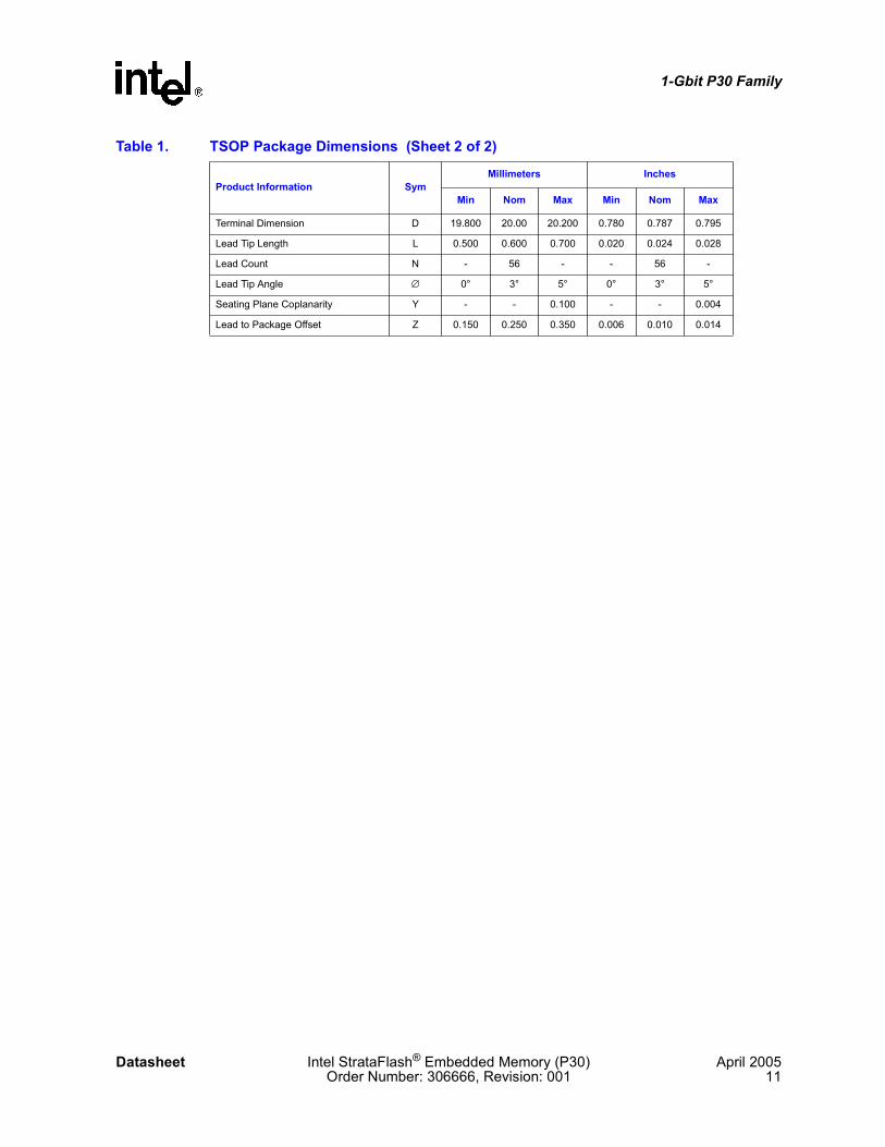


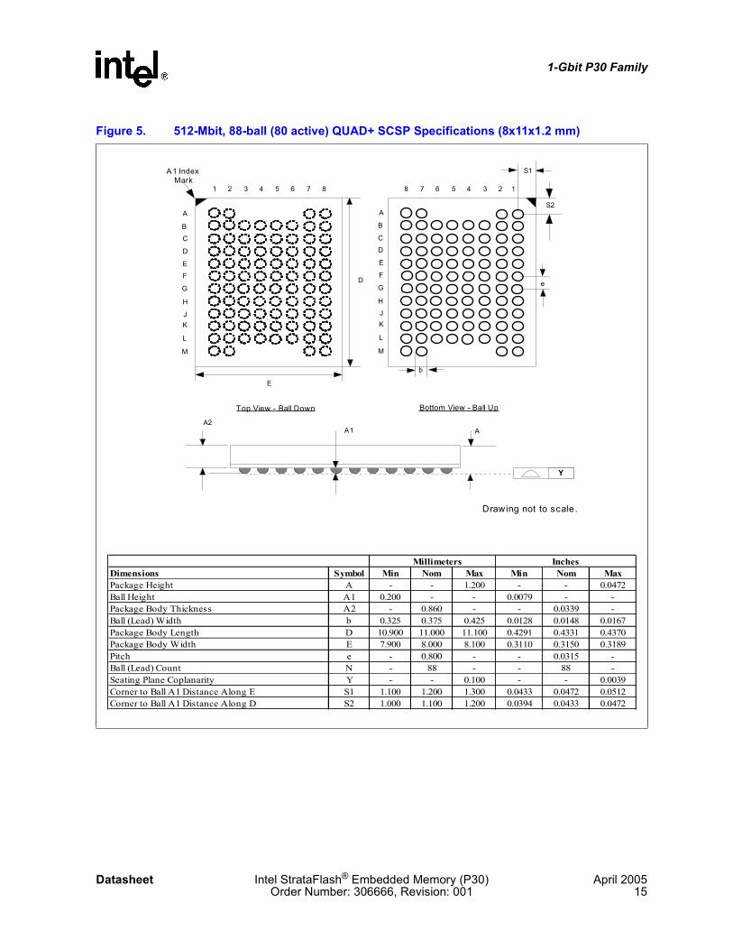


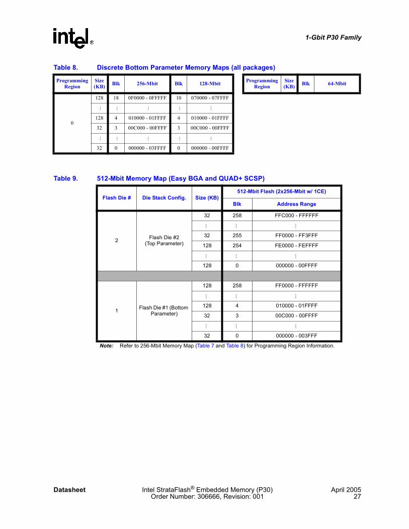

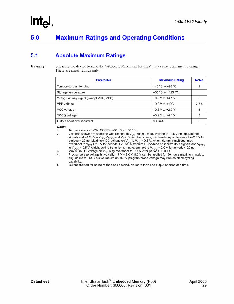

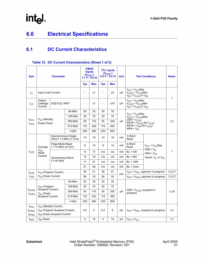

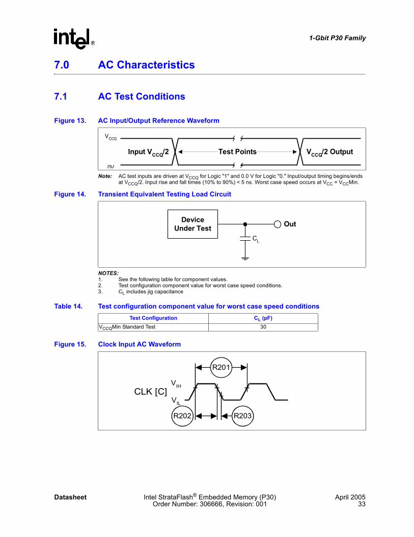


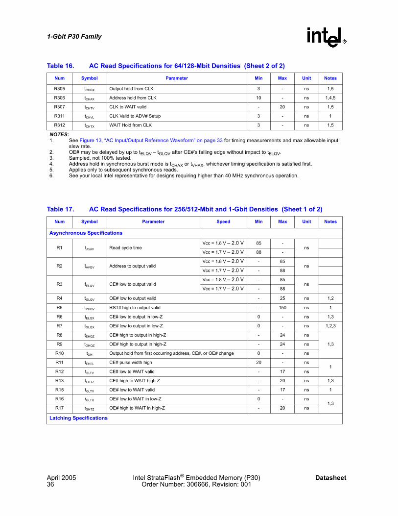
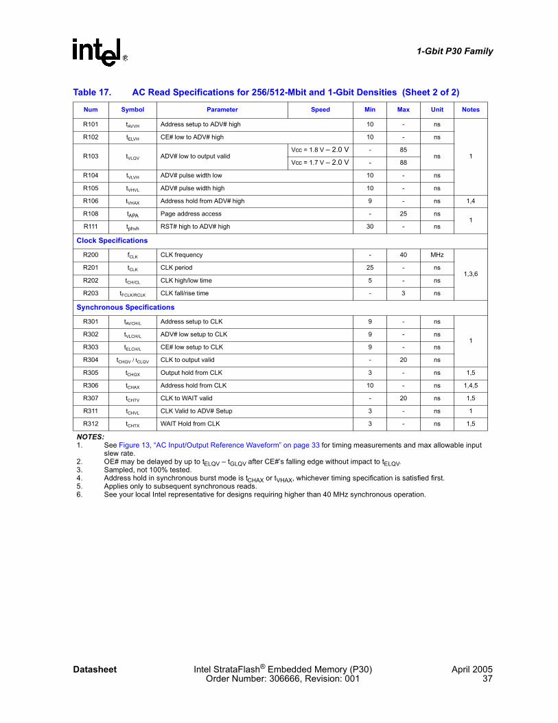

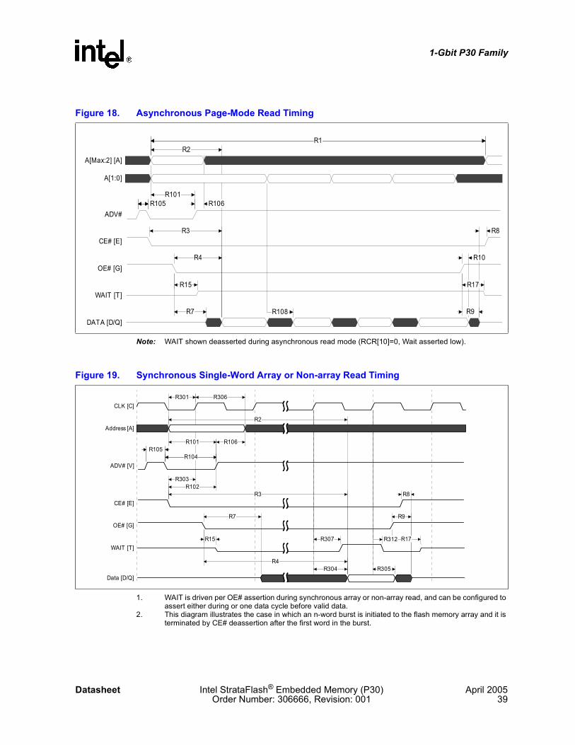


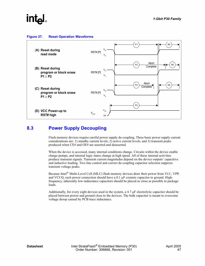


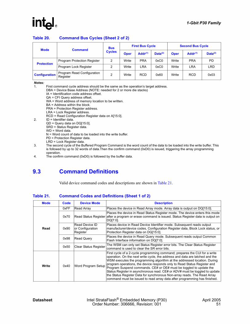


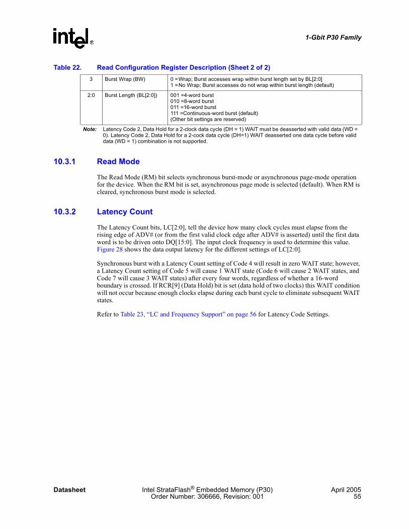


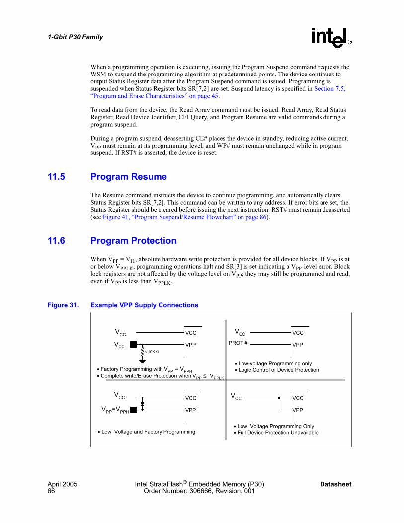


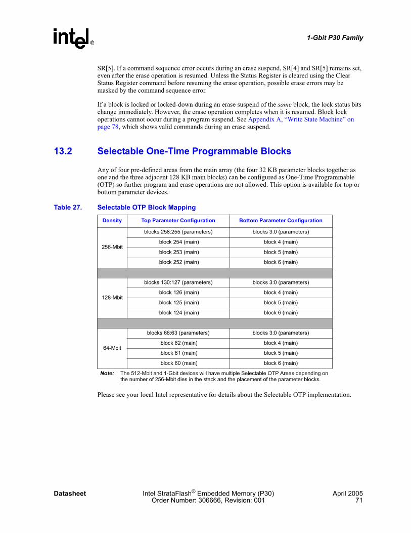


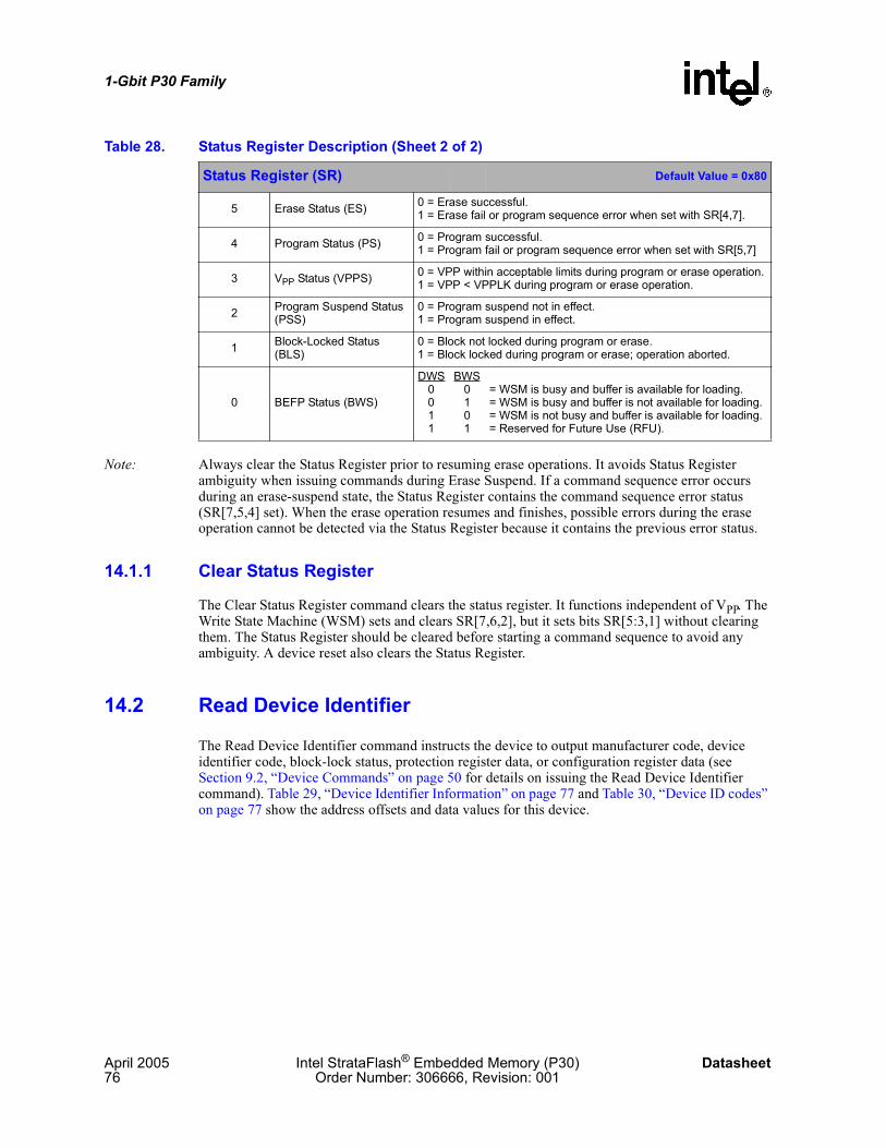

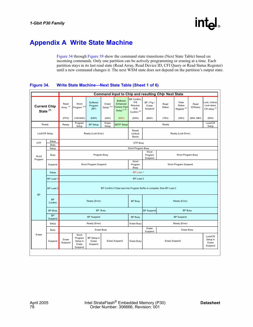

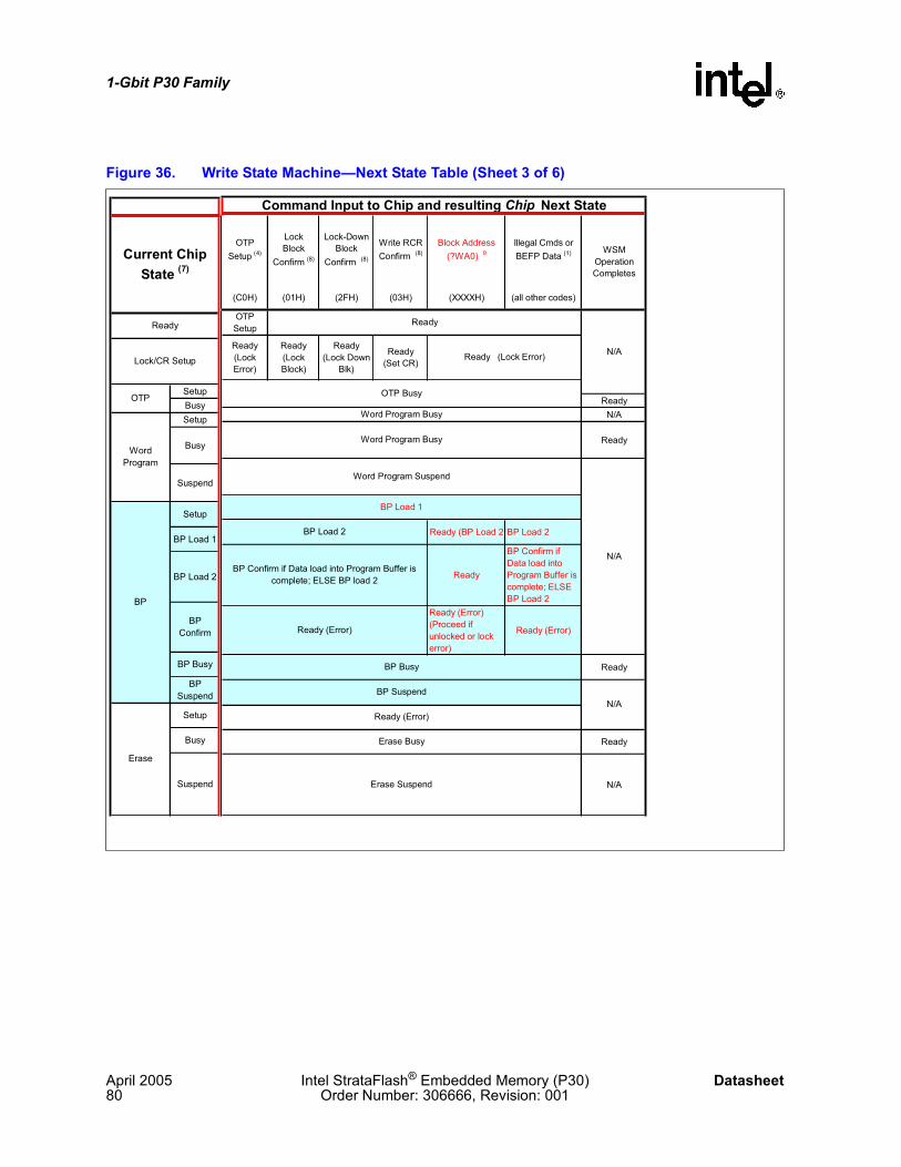

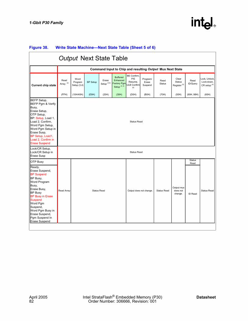


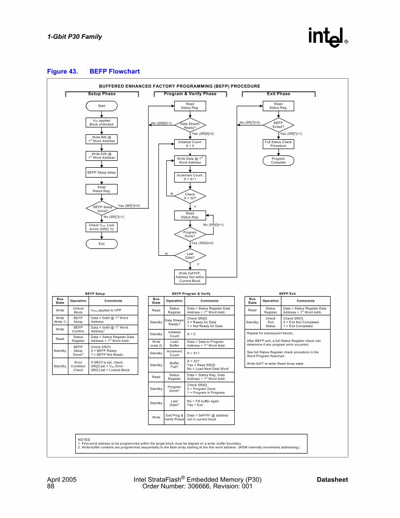


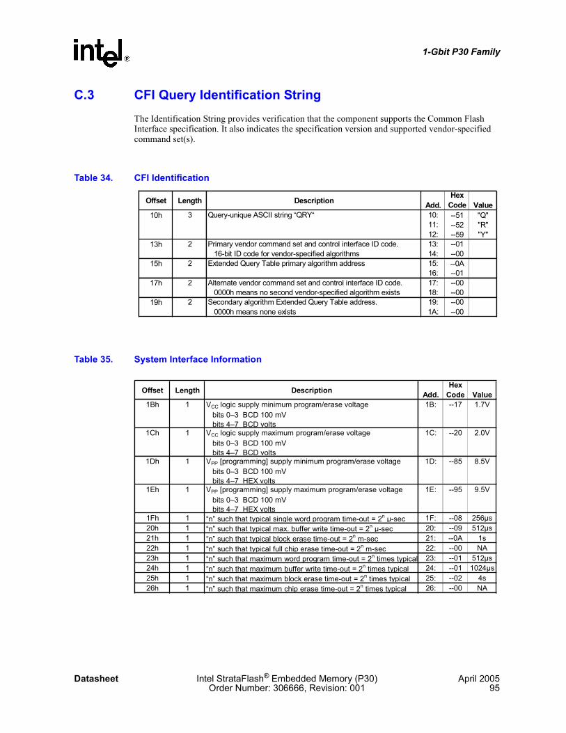

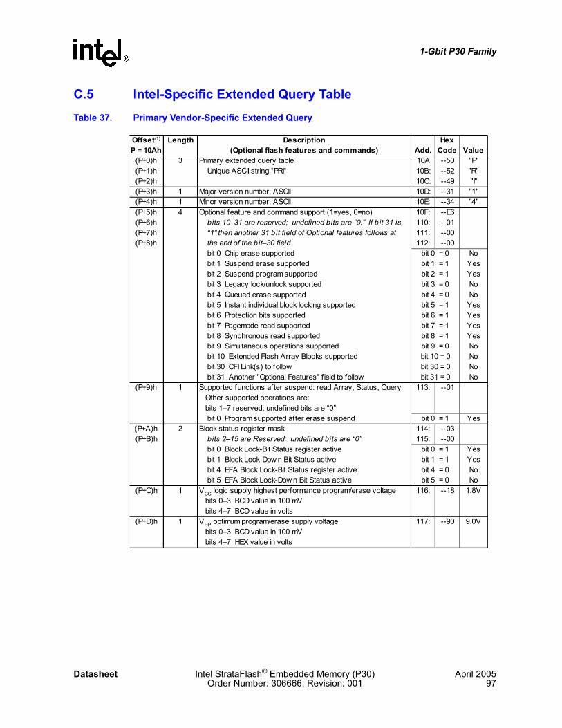


![MODBUS Protocol for MiCOM P30 Series - … · MODBUS Protocol for MiCOM P30 Series [ [[ [Substation Protocols ]]]] 3 Mbm0100b.doc Schneider Electric Energy MiCOM P30, MODBUS](https://static.documents.pub/doc/80x56/5b97ad7d09d3f2dc628b49b6/modbus-protocol-for-micom-p30-series-modbus-protocol-for-micom-p30-series.jpg)


