Figure 4.13 - Path Delay Profiles for 2mm Wire in 180nm l x l x 87
Figure 4.14 - Delay Breakdown for 0.5mm Wire 97
Figure 4.15 - Delay Breakdown for 2.0mm Wire 98
Figure 4.16 - Delay Breakdown for 3.0mm Wire 98
Figure 4.17 - Early Turn Routing Example for L4 Wires 101
Figure 4.18 - Routing Choices Due to Fast Paths with Early Turns in an L4 Architecture
103
viii
A c k n o w l e d g e m e n t s
I would to like thank my academic supervisors Dr. Guy Lemieux and Dr. Shahriar
Mirabbasi for their advice, teachings and support throughout my graduate degree. I am
very fortunate to have two professors who have taught me a great deal about research and
the technical aspects of our field.
I would also like to thank the faculty and staff of the SOC lab for making the lab a
wonderful academic home. Thanks for making me feel welcome and always offering
assistance. M y gratitude goes out to all the members of the FPGA and analogue research
group for their many helpful insights and of course, excellent company.
I am grateful for the use of the Westgrid computing resources at U B C . Much of the
research in this thesis was facilitated through the use of Westgrid.
Finally, I would like to thank my family for their constant support and enthusiasm.
ix
C h a p t e r 1
I n t r o d u c t i o n
Field-programmable gate arrays (FPGAs) are large integrated circuits comprised of blocks of
programmable logic interconnected with programmable routing circuits. The demand for
increasing their performance has driven FPGA designers in search of the latest process
technologies. With each new technology generation, FPGAs have grown larger and increasingly.
dense, providing more logic with a smaller feature size. As one can expect, the wiring demands
of these devices have also increased.
In deep submicron process technologies, interconnect has been identified as one of the most
critical challenges facing integrated circuit designers [1]. In an FPGA, this is even more
important, as 60-80% of the delay is caused by the interconnect [2]. Although extensive efforts
have been made on interconnect optimization by means of repeater insertion for ASIC designs,
few studies have investigated the optimization of circuit design for FPGA interconnect.
Techniques used in general ASIC interconnect optimization cannot be directly applied
because the FPGA interconnect design problem is different in nature. Fortunately, due to its rigid
structure and point to point nature, the topology of FPGA interconnect does not possess the
complex fanout trees found in ASIC designs as seen in Figure 1.1.
1
Figure 1.1 - Routing Example of a Net in an ASIC
Instead, routing resources in an FPGA are made up of long straight wires which make up the
predetermined paths of the routing resource architecture, as shown in Figure 1.2. This
simplification is welcome as it considerably reduces the complexity of the circuit design problem.
However, it is not without its own challenges.
Figure 1.2 - Routing Example of a Net in an F P G A
Like an ASIC, wires still fanout to numerous points in FPGAs, but whether or not a fanout is
used in an FPGA interconnect is not known until after a user circuit is fully implemented.
During operation, the path of a signal can occupy either a part or the entire length of a wire. Our
experiments have demonstrated that 50% to 87% of signal paths in an FPGA routing solution
leave the wire before arriving at the end. Such turns are called early turns (Figure 1.3). In order
to assess early turn delays, this work will often consider the delay to several points along the
interior of a wire. In general, these delays are referred to as the midpoint delays of a wire. To
the author's knowledge, the concept of early turns and midpoint delay has not been previously
examined in FPGA research.
The other major difference between FPGA and ASIC interconnect is that the FPGA
interconnect must be programmable. This requirement introduces multiplexer circuits which can
2
adversely affect delay. The closed form models often used in. the development of general
interconnect optimization techniques are less accurate at modeling such circuits, making it
difficult to apply the techniques from previous work on FPGAs. While closed-form analytical
techniques are useful for rough approximations, they are not accurate enough to compare
significantly different circuit implementations. This accuracy is vital to obtaining the best
possible speed performance from FPGAs.
Figure 1.3 presents an example of an FPGA interconnect made up of wires, multiplexers and
drivers. This research attempts to address the problem of wire delay in FPGAs by developing an
accurate approach to design and evaluate interconnect driver circuits for FPGAs.
FPGA Interconnect
Figure 1.3 - Example of F P G A Interconnect
By taking advantage of the recent shift to FPGA architectures with a single driver per wire [3], it
is possible to reduce midpoint delays, in addition to end-to-end (or endpoint) delay, to speed up
performance in FPGAs through the use of distributed driver designs. As an example, Figure 1.4
presents a distributed driver design which could be used to implement the interconnect switch
driver and the programmable wire in Figure 1.3. This sample driver circuit is made up of 2
distributed drivers of size BO and B I . Using a path delay profile (PDP), the delay of the signal
can be examined from its origin to the end of the wire, or to any point in between. PDPs for two
3
designs, a lumped driver and a distributed driver, are shown in Figure 1.4. It can be seen that the
midpoint delays of the first half of the wire are significantly faster than midpoint delays of the
lumped-design PDP. This indicates that distributed driver design has the potential to improve the
delay of the early turn shown in Figure 1.3.
0% 30% 50% 100%
Distance Travelled Along Wire
Figure 1.4 - Example of a Switch Dr ive r Path Delay Profile Using modified C A D tools, it is possible to model the improvements from these circuit designs.
Our results demonstrate that critical path delay due to these improved circuit designs can be
reduced by up to 46%.
1.1 Motivations and Objectives
In the past, it was not possible to consider interconnect optimization techniques, such as
repeater insertion, on FPGA wires because a long wire was shared by multiple tri-state drivers
located at different points along the interconnect. In [3], it was shown that implementing
directional wires with a single, lumped driver at the beginning of the wire improves both the
4 .
delay and area efficiency of an FPGA architecture. One way to take further advantage of
directional wires that was not explored in [3] is to uniformly insert additional repeaters in order
to reduce the delay of the wire.
The impact on FPGA performance from the use of additional repeaters is, as yet, unclear.
Distributed buffering, has potential to improve not only endpoint delay, but midpoint delays as
well. This is of particular benefit to FPGA designs as signals often turn off a wire before
reaching the end. However, the only way to determine how much of a wire is used is by routing
circuits on the FPGA using C A D tools. A large component of this research is to assess circuit
design options using a C A D model which accurately considers the impact of early turns on
critical path delay.
1.2 Contributions
The contributions of this research are a circuit design methodology and evaluation of
interconnect drivers for long wires in FPGAs to improve midpoint delays and end-to-end delay.
Key findings of this work can be organized into three categories: circuit design, FPGA
architecture and C A D modeling.
Circuit Desifin
• A circuit design methodology for FPGAs was produced which when given a fixed
wirelength, can determine the number of buffers, size of buffers and spacing between
buffers to achieve near-optimal delay.
• Using the circuit design approach, it is shown that distributed buffering is effective at
reducing delay for wires, but only i f the wires are of sufficient length (greater than 2mm
in a 180nm technology with a minimally spaced and minimally sized wire)
5
FPGA Architecture
• Increasing the length of the wire between multiplexers (switch boxes) can improve the
signal velocity and achieve near-ASIC interconnect speeds.
• Turns at the end of a wire (normal turns) are not critical. As fast paths and proper turn
modeling are introduced, the frequency of normal turns decreases. Also, 50-87% of turns
are before the end of the wire. These facts suggest that it maybe possible to remove or
reduce frequency of normal turns in the architecture.
• Fast paths through the switch block multiplexer were verified to improve critical path
delay by up to 8% for short architectural wirelengths.
C A D Modeling
• FPGA C A D tools which are capable of improved modeling were developed and used to
evaluate proposed circuit designs. The improved modeling alone resulted in a 10%
improvement in critical path delay.
• Distributed buffering yields a modest delay improvement of about 3%.
1.3 Overview
This thesis is composed of 5 chapters. Chapter 2 starts with an overview of FPGA architecture
and C A D , and presents concepts of interconnect design theory. Chapter 3 presents the circuit
design of FPGA interconnect drivers by providing detail on the development of a driver design
methodology. Chapter 4 describes the modeling improvements incorporated into FPGA C A D
tools which were used to assess the circuit designs produced in the previous chapter. Finally,
Chapter 5 summarizes the conclusions drawn throughout the thesis and provides suggestions for
future work.
6
Chapter 2
Background
In this chapter, the background information for this thesis is presented. The first half presents
an overview of FPGA architecture and the supporting C A D flow. Particular emphasis will be
placed upon the topics related to routing.
The second half of this chapter is focused on interconnect design theory. This section presents
methods used for designing and optimizing interconnects in deep-submicron integrated circuits.
Important fundamentals such as device parasitics, wire models and interconnect driver design
techniques will be described in detail.
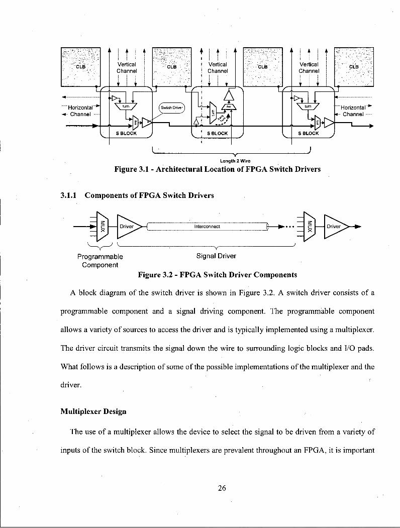
2.1 FPGA Overview
An FPGA is an integrated circuit equipped with programmable logic and programmable
routing resources. The reconfigurable elements allow an FPGA to be programmed after
fabrication to implement virtually any digital logic function. The majority of FPGAs provide
programmable logic using lookup tables (LUTs). An individual k-input lookup table, or k-LUT,
is capable of implementing any k-input combinational logic function. In order to support
sequential logic, flips flops are placed at the LUT output; this combination is referred to as a
basic logic element (BLE). In most modern FPGAs, BLEs are grouped together in larger blocks
called configurable logic blocks (CLBs) and are configured using S R A M memory elements.
7
Connectivity between logic blocks is achieved through the programmable routing resources.
These resources are made up of metal tracks arranged in channels running vertically and
horizontally across the FPGA. A channel is made up of a number of tracks, typically referred to
as the channel width. A track is made up of wire segments of fixed length. These wire segments
are placed end-to-end to span the length of the channel. The architectural or logical length of a
wire is defined by the number of CLBs it spans. The physical length of a wire is equal to the
logical length times the physical width of the C L B layout tile. Wires are connected to each other
using switch blocks, and to the logic blocks using connection blocks.
Figure 2.1 presents a typical mesh or island-style FPGA architecture which is assumed in this
work. An example of an architectural length 2 wire, also denoted as L2, is indicated. The
connection blocks are labeled as C blocks and the switch blocks are labeled as S blocks.
This work is focused on the transistor-level circuits inside the switch blocks which are located
at the intersection of horizontal and vertical channels. These blocks contain multiplexers which
connect tracks together across the intersection in predefined patterns [4]. The switch block
contains large buffers that are used to drive the long metal traces which make up the wire
segment. These buffers occupy considerable area in the switch block which represents a
significant proportion (roughly 1/3) of overall FPGA area [4].
8
Length 2 Tracks/Wire^
Vertical ^Channel
CLB
= r V :
_
CLB 1
CLB CLB
I |
I | - \\
11 C \
8 v J
1 1
• i l 11
Horizontal Channel
S BLOCK
Figure 2.1 - F P G A Architecture with Switch Block Detail
2.1.1 Routing
The functional design of these interconnect circuits is governed by the routing resource
architecture. The routing resource architecture defines the precise connections and turns a signal
may follow in the routing resource network. There are two main routing resource architectures:
bidirectional and unidirectional.
9
Bidirectional Architecture
' C block i
Shared Track / Wire
S block C block
Figure 2.2 - Representation of a Wire in a Bidirectional Architecture
In a bidirectional routing network (Figure 2.2), a wire can transmit a signal in either direction.
This approach provides a more flexible routing network which allows efficient use of available
metal tracks. This means that the drivers of these wires must be tristate drivers so they can be
disabled when not in use.
Interconnect
\ x n w /
Figure 2.3 - Tristate Driver Example
A common approach to building tristate buffers in FPGAs is to use an NMOS passgate placed
at the output of the regular driver (Figure 2.3) [5]. The use of this design confines the layout of
the driver near to the point where the driver is connected to the wire. This means the driver
design cannot be distributed along the wire. The output passgate affects both speed and area
negatively by adding resistance to the output drive, producing a V T drop in the signal swing, and
adding area to the circuit layout. Furthermore, since only one of the tristate drivers connected to
10
each wire can be enabled after programming, this approach causes a significant waste of active
area.
Unidirectional Architecture
C block
Track / Wire
Track / Wire
C block S block
Figure 2.4 - Representation of a Wire in a Unidirectional, Single-Driver Architecture
In a unidirectional routing network (Figure 2.4), each track can only transmit data in one
direction. This topology reduces the flexibility of the routing resources and suggests that the
channels contain pairs of wires. Despite this restriction, work done in [3] demonstrates that this
approach is more efficient in terms of area and provides improved delay over the bidirectional
architecture.
J Z MUX
\ x n i / M /
Interconnect 6- • • • Interconnect
1 Figure 2.5 - Unidirectional Driver Example
An additional restriction known as single-driver wiring ensures each wire is only driven by
one driver, as opposed to multiple drivers as in the bidirectional architecture (Figure 2.5). This
simplifies the routing network, eliminating the ability to connect at arbitrary points in the middle
11
of the wire. Instead, C L B outputs can only connect to the starting-points of nearby wires. A key
benefit of this is that tristate operation is no longer required. Note, however, that the buffers,
which make up the driver no longer have to be in the physical vicinity of the source. Instead,
they can be located at various positions along the length of the wire. In this research, it is shown
that the relaxation of this constraint can produce an improvement in the delay of the wire
segment, particularly when the wire is of sufficient length.
2.1.2 F P G A C A D Flow
Before a user's logic circuit can be implemented on an FPGA it must under go certain
processing steps known as the FPGA design flow to map the circuit onto an FPGA device. The
FPGA C A D flow is comprised of 5 main steps: synthesis, technology mapping, clustering,
placement and routing.
The first two steps in the C A D flow are synthesis and technology mapping. In these steps, the
circuit is converted from a hardware description language into a network of FPGA-specific logic
blocks which implement the functionality of the original circuit. After this point, logic blocks in
the network are grouped together into clusters during the clustering step. This step controls the
number of BLEs which are packed into a C L B and can be used as a rough method to manipulate
the overall size of the circuit implementation on an FPGA. The following steps are placement
and routing. Placement determines the locations for each C L B on an FPGA device. Routing uses
detailed information of the FPGA routing resources to efficiently connect all the clusters
together and implement the connections between logic blocks. In this work, particular emphasis
is placed on developing the model of the routing resources used in the routing step.
12
F P G A C A D Experimental Methodology
The standard FPGA C A D experimental methodology involves running a suite of user circuits
as benchmarks through the C A D flow multiple times, each time modifying the C A D step under
study. In this work, the first 4 C A D flow steps are applied once on each benchmark circuit. The
final step, routing, is applied multiple times. The first time the router runs, it searches for the
lowest channel width which can successfully route the circuit design. Once this value is
determined, it is increased by one complete set1 of directional tracks to produce a new larger
channel width. The router is run again, but this time it only routes the design once using the new
calculated channel width. This gives some flexibility to the router, which tends to improve the
quality (delay performance) of the routing results.
2.1.3 VPRx
For the place and route steps in the C A D flow, the academic tool V P R [6] is used. A heavily
modified version, known as VPRx [3,4], is used because it supports unidirectional wiring. Both
VPR and VPRx use the same core routing and delay calculation algorithms. In the following two
subsections, details on the routing resource graph and the VPRx delay model is provided.
Routing Resource Graph
VPRx models all routing paths in the FPGA using a routing resource graph. This data
structure represents all possible connections which can occur in the FPGA routing network. In
essence, the routing resource graph is a directed graph of wires, switches and pins at different
locations on the FPGA. In the graph, wires and pins are represented as nodes while switches
1 The number of tracks in a set is equal to twice the architectural length. Further details can be found in [3].
13
between wires are represented as directed edges connecting nodes. Figure 2.6 presents the
routing resource graph for a set of logic blocks connected by two wires. In this example, the
bidirectional switch on wire 1 is modeled as a pair of directed edges, where the directional
switch on wire 2 has only one edge.
Logic Block A
• E Logic
Block B
A in A in2 H B_out
• E l • wire 3
wire 4
1 SRAM
Input Pin of the Logic Block
Output Pin of the Logic Block
Switch Block
wire 1
wire 2
wire 1
wire 3
A in1
B out
sink
Figure 2.6 - Example of a Rout ing Resource G r a p h [6]
wire 2
wire 4
A in2
Delay Calculat ion
The routing algorithm used in VPRx is a modified version of the Pathfinder routing algorithm
[6, 7]. This algorithm uses the Elmore delay calculation [8] as the primary metric to optimize the
delay of routing paths. For this reason, it is important to ensure that the delay calculation is
accurate. Fortunately, the routing resource graph is designed to facilitate the calculation of the
delay of a signal path through the graph. Each node in the graph contains the capacitance and
resistance of the wire being modeled. Similarly, each switch edge contains the delay of the
switch, its input capacitance, output capacitance and its ability to drive an RC load in the form of
an equivalent resistance. VPRx uses an incremental Elmore approach to calculate the delay [6].
14
The Elmore delay to a given node in an RC tree can be calculated by iterating over all the
capacitances in the tree. For a signal path with no branches, this computation is straightforward.
As the router expands along the routing resource graph, the delay of the next node is computed
incrementally by adding the contribution of its parasitics to a running delay value. The equation
used at each node is tdel =tdel + Rupslream x C n o d e . The value of Rupstream is increased as the nodes are
added to the routing solution. This approach works well for calculating the approach to the end
of an RC tree where there are no fanouts to add extra capacitive loading. Greater detail on
Elmore delay calculations will be described shortly in Section 2.2.2
2.2 Interconnect Design Theory
Interconnect design is an increasingly important consideration for integrated circuits built on
deep-submicron process technologies. In this section, background on interconnect design is
presented to provide the reader with an understanding of tools and techniques used to design
circuits which drive interconnects. Topics such as interconnect models and interconnect driver
design techniques are provided to ensure that the reader is familiar with the concepts in the
subsequent chapters.
2.2.1 Deep-Submicron Interconnect
Interconnect in deep-submicron process technologies has several important issues that affect
the performance and design of high speed circuits. Problems such as signal integrity, inductive
coupling, IR drop and electromigration are among the many growing challenges which face IC
designers. However, the most prevalent challenge for interconnect design in deep-submicron
design is signal delay.
15
The primary factors controlling interconnect delay are wire parasitics. The parasitics of
interest, resistance (R) and capacitance (C), are physical properties of the wire. The resistance
and capacitance of an interconnect act like an RC load in the signal path which causes
propagation delay. The amount of resistance and capacitance is determined by the physical
dimensions of the interconnect and the materials used.
Parasitic Resistance
The resistance is determined from the cross-sectional area of the interconnect. A larger area
implies a lower resistance. However, as technology shrinks, wires in nanometer technologies
tend to be thinner than before. The overall effect is an increase in parasitic resistance for a
minimum width wire. For example, the resistance of a minimum sized wire in 90nm is roughly
twice the resistance of a minimum sized wire in 180nm.
Improved materials such as copper interconnect have been introduced in order to reduce
interconnect resistance. At most, this provides a one-time improvement; the resistance continues
to increase as wire geometries continue to shrink. In the meantime, the most straightforward
solution is to increase the wire width in order to reduce resistance. Unfortunately, this is not
always possible because an increase in wiring density is needed to keep up with the increase in
logic density as transistors are scaled.
Parasitic Capacitance
Parasitic capacitance of an interconnect is caused by coupling with neighboring conductors.
The amount of capacitance is related to the ratio of the conductive areas facing each other to the
distance separating the two conductors. Figure 2.7 shows a typical construction of a deep-
submicron interconnect with the most dominant parasitic capacitances labeled. Plate capacitance
16
is caused by the area at the top and bottom of the wire. In earlier technologies, this value was the
dominant factor. However, with the narrower wires in nanometer technologies, the coupling
capacitance has grown to be the major capacitance contribution.
Thus far, the geometry issues of interconnect have not been discussed. In most FPGAs, long
interconnects are manufactured on mid-level layers (e.g., metal 3 in a 6 metal process).
Therefore this work assumes that metal layer 3 is used to build the wires. Two combinations of
wire widths and spacings were considered for 180nm and 90nm process technologies: l x
minimum width/lx minimum spacing (denoted as l x l x ) and 2x minimum width/2x minimum
spacing (2x2x). Results are presented for designs built using 180nm l x l x and 90nm 2x2x
interconnects. These combinations are chosen because they represent the range of delays
achievable, as 180nm l x l x is the slowest and 90nm 2x2x is the fastest.
35
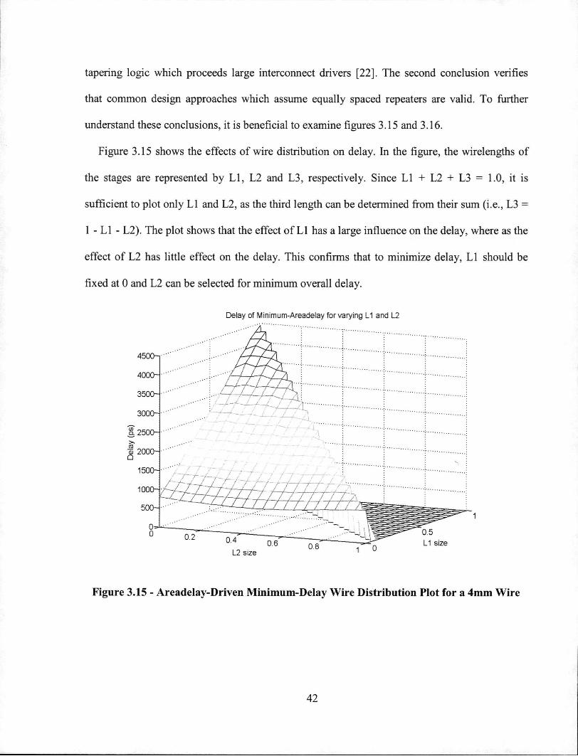
3.2 Rapid Design Space Exploration
By developing a model based on the design parameters from the previous section, the general
problem of sizing and placing buffers on a wire can be explored. A quick-to-compute Elmore
model is created and used to rapidly explore the design space of a system with three buffers. The
results from this exploration suggest that distributed buffering can improve results at certain
wirelengths. Furthermore, the results indicate that the design space is fairly insensitive to small
changes in buffer size and wirelength, which allows for some flexibility in choosing an optimal
design.
3.2.1 Ana ly t ica l Delay M o d e l
In this study, the design parameters will be exhaustively swept using a simple Elmore delay
model. The difference between this exploration and previous work [14, 22, 23, 32] is that the
search here does not impose relationships between subsequent inverters. Most approaches
constraint the size of successive inverters to be equal or related to one another based on a
geometric series. Unfortunately, by not introducing any constraints, the design space becomes
very large and unwieldy. To reduce the dimensionality of the design space, the number of stages
is restricted to 3 stages as in previous FPGA switch driver designs [3, 33]. Another constraint is
that the size of the first inverter is fixed to minimum. This is done because the Elmore model
approach does not take into account the input capacitance of the first gate. Also, using a smaller
sized buffer will minimize the impact of loading on the preceding circuitry.
The delay model uses standard VLSI techniques [12] presented in the background. Figure
3.12 shows a buffer of size s driving a wireload of length / and a downstream buffer of size s'.
36
Figure 3.12 - Elmore Model of Buffer & Wire Delay
The Elmore delay equation for the wire has the time constant:
T = —(c0s + cl + cgs') + ̂ Y- + (rlxcgs') ^
where r and c are the resistance and capacitance per unit length of a wire, c0 and cg are the output
and input capacitance of a minimum sized buffer and rx is the equivalent resistance of a
minimum-sized transistor. Although the value of rx depends on the type of transistor used, most
approaches do not distinguish the value. In this work, the Elmore-delay computation code
distinguishes between a rising and falling scenario and takes the average of the delays. Table 3.3
lists typical values of the parasitics in a 180nm process technology.
Parasitics in 180nm Process Technology Parameter Description Typical Values [12]
Co Output capacitance 1 fF/um cs Gate Capacitance 2 fF/ urn c Wire capacitance per unit length (min width & spacing) 0.1-0.25 fF/um r Wire resistance per unit length (min width) 125-300 mQ/um
rP Equivalent resistance of a PMOS transistor 30 kQ/um rn
Equivalent resistance of an NMOS transistor 12.5 kQ/um Table 3.3 - Typical Parasitics in Deep Submicron Process Technology
The total delay through the chain of inverters is calculated by summing up the delay through
all three stages. Typical Elmore delay modeling applies a ln(2) = 0.69 factor to x to calculate
50% propagation delay, however, it was found that a l.Ox factor was more accurate due to the
37
non-ideal (ramp) inputs used to drive the circuits [12]. With this model, the delay of a three-stage
driver for any given combination of inverter sizes, inverter spacings and total wirelength can be
calculated.
driversize sweep
wire distribution sweep
L 1
Figure 3.13 - Parameters Being Swept
3.2.2 Design Space Sweeps
Using the general delay model, a set of nested sweeps was used to search the design space for
a variety of wirelengths. The inner sweep is a driver-size sweep and the outer sweep is a wire-
distribution sweep. The driver-size sweep calculates the delay for all possible combinations of a
set of predetermined buffer sizes. From the sweep, the buffer sizes which produce the smallest
delay and the smallest area-delay product can be determined. Similarly, the wire-distribution
sweep generates the best buffer spacing configuration for each wirelength setting. The pseudo
code for this exhaustive search is shown in Figure 3.14. This pseudo-code was implemented in
Matlab. The calculate_delay_of_() function computes the Elmore delay as described in the
previous section (3.2.1).
38
driver_sizes_weep(wirelengths_array [wl w2 w3]) { /* mindelaymetric can represent delay or areadelay */ mindelaymetric = largenumber; for a l l b l s i z e s [bl] {
for a l l b2sizes [b2] { for a l l b3sizes [b3] {
/ * b u i l d c i r c u i t with b u f f e r s i z e s [bl b2 b3] and w i r e d i s t r i b u t i o n s [wl w2 w3] */
c i r c u i t = b u i l d _ c i r c u i t ( [bl, b2, b3], [wl w2 w3] ); delaymetric (bl,b2,b3) = ca l c u l a t e _ d e l a y _ o f ( c i r c u i t ); /* Grab the best design */ i f (delaymetric (bl,b2,b3) < mindelaymetric) {
mindelaymetric = delaymetric (bl,b2,b3); b e s t c i r c u i t = c i r c u i t ;
} }
} } return b e s t c i r c u i t ; }
wire_distribution_sweep(wirelength) { /* mindelaymetric can represent delay or areadelay */ mindelaymetric = largenumber; fo r a l l Lllengths [LI] {
for a l l L21engths [L2] { L3 = wirelength - LI - L2 ; c i r c u i t = driver_sizesweep([LI L2 L3]) delaymetric (L1,L2) = calc u l a t e _ d e l a y _ o f ( c i r c u i t ); /* Grab the best design */ i f (delaymetric (L1,L2) < mindelaymetric)
delaymetric = delay (Ll,L2); b e s t c i r c u i t = c i r c u i t ;
} ' } return b e s t c i r c u i t ;
}
Figure 3.14 - Design Space Sweep Pseudo Code
3.2.3 Results
Table 3.4 presents the best wire distribution, buffer sizes and resulting delays for wirelengths
ranging from 1mm to 16mm in a 180nm process using wires with l x minimum spacing and lx
minimum width. The best wire distribution is shown as three values which represent the length
of wire following buffer 1, 2 and 3, respectively, these values are normalized to the total
wirelength and sum to 1.0. Similarly, best buffer sizes are listed as the size of buffer 1, 2 and 3,
respectively. The delay for the best design is shown in column 4 and the delay for the
corresponding lumped design is shown in column 5. The final column indicates the performance
39
difference between the two designs. For example, the 2.5mm design is made up of lx , 7x and
38x buffers followed by wirelengths which make up 0%, 15% and 85% of the total wirelength,
respectively. This design has a delay of 379.8ps. In comparison, the best 3 stage lumped design
for a 2.5mm design would have a delay of 382.3ps, approximately 1% slower.
With only three stages in this design, it is unlikely that any wires as longer than 4-5mm will
even be considered. Data for wirelengths up to the 16mm long are shown because that is when
the design becomes fully uniform. The most interesting region is around 2-3mm, where the best
designs begin to shift from lumped designs to distributed designs.
Table 4.8 - Turn Count Changes Due to Addition of Distributed Features
One thing which has not been examined is where the early turns took place. It is possible that
the location of the early turns is influenced by new circuit designs. Ideally, the router would be
able to strategically choose the best location for an early turn based on the staggered delay
profile of the distributed drive design. Unfortunately, without data indicating the location of
early turns, no clear conclusions can be drawn.
4.4.6 Runtime
Although not a major focus of this work, runtime is an important factor which must be
considered by all C A D tools. By introducing the detailed circuit models which enlarged the
routing resource graph, the complexity and therefore runtime, of the routing problem increased
considerably. The amount the routing resource graph grows is largely dependant on the
architectural length of the wires being modeled. In this work, architectural length of L4 and LI 6
are used. For L4 designs, adding E T M increases runtimes by up to 3x. For the LI 6 designs,
runtimes increase considerably, ranging from 3x up to almost 30x depending on the modeling
options enabled in the experiment. The largest increases in runtime are observed in experiments
involving only E T M .
An interesting observation is that all the experiments which had Fast Path enabled had
runtimes only 3-16x larger than the original. It appears that providing a routing option as
104
compelling as the fast path helps to reduce the runtime of the routing process. In the standard
configuration without the fast path, the router has to negotiate between three equally slow
choices. Introducing the fast path makes the best choice obvious. This allows the router to
postpone expansion of slower neighboring nodes enough to reduce the overall routing runtime.
This observation is useful because it shows that runtime can be reduced by providing clear
choices for the router to pursue.
105
Chapter 5
Conclusions and Future Work
As the industry moves towards faster clock speeds and smaller devices, the challenge of
interconnect delay will always be present. For FPGA designers, this is a significant concern as
the wiring demands of programmable interconnects are intense.
In this thesis, an attempt has been made to address the interconnect delay problem by
investigating the design of programmable switch drivers for FPGAs. Our resulting circuit
designs are based on routing architectures which were recommended by [3]. Prior to [3], FPGA
routing architectures used shared wires that were driven from various points throughout the wire.
This resulted in all FPGA drivers having tristate capability which restricted driver designs to
lumped circuit architectures. In [3], it was shown that implementing directional wires with
single-drivers can improve both the delay and area efficiency of an FPGA architecture. This
thesis shows that by using directional wiring with single-drivers, it is possible to design circuits
which can optimize the interconnect performance on FPGA wires. Optimized circuit designs are
generated using a circuit design methodology which is capable of estimating the delay of a
circuit design using SPICE generated delay data. The use of this method provides the flexibility
and accuracy obtained from a SPICE-level simulator but has the advantage of shorter runtime.
By examining the PDP of the optimized circuits, it can be seen that distributed driver designs
can offer more to FPGAs than just improved endpoint delay. In comparison to lumped driver
106
designs, distributed driver designs can improve early turns which occur before the end of the
wire. Using an enhanced version of VPR capable of accurately modeling the new circuits, the
performance of several circuit designs were evaluated using standard benchmarks. Results show
that early turn improvements alone can reduce delay by a modest amount of about 3%. Overall,
the effects of the new circuits are substantial. When the benefits from improved modeling,
optimized circuit design and other enhancements such as fast paths and faster multiplexers are
combined, reductions in critical path delay by as much as 46% are observed.
By examining the optimized circuit designs, several items which are useful to an FPGA
architect are revealed. The first is that distributed buffering only outperforms lumped designs
once wires are long enough. Results show that in 180nm technology, wires less than 2.0mm
cannot reap the rewards of distributed buffering. The second discovery is that the length of the
interconnect has particular influence on the best speed (delay-per-millimeter) at which the wire
can transmit a signal. In the case of FPGAs, this means that using longer wires can help to
achieve speeds closer to those found in general ASIC interconnect. This information is useful to
an FPGA architect as it aids in the selection of wirelengths for long wires.
5.1 Future Work
This work has attempted to lay the preliminary ground work for further research into
interconnect optimization for FPGAs. As long as FPGAs continue to use wires, approaches to
reduce delay will be welcome. Since this research is mainly divided into two parts,
recommendations are grouped into two categories: Circuit design and C A D .
107
5.1.1 Circuit Design
There are numerous choices involved in the circuit design approach. Some related to circuit
design and other related to modeling. The following topics present some suggestions on future
work related to the circuit design component of this work.
Advanced circuits
The SPICE simulator allows complex circuits to be simulated with great accuracy. This opens
the door to a large variety of circuits which do not have an equivalent Elmore model. Low swing
signaling circuits can offer reduced power consumption and higher performance. For noise
immunity, one can consider the benefits of differential circuits as well.
Noise Modeling
Throughout this work, the effect of deep-submicron challenges were mentioned, but not
directly addressed. Noise from inductance and coupling capacitance can impact performance and
functionality of the circuits.
Coupling capacitance is typically modeled using the Miller Coupling Factor. In this work, it is
assumed that there are no transitions on surrounding wires. Work done in [26] shows that the
Miller Coupling Factor does not affect trends, but it will certainly affect the absolute values of
the resulting design.
Similarly, modeling of inductance is recommended. Unfortunately, assessing the amount of
inductances will be very difficult without prior knowledge of the IC layout. However, since the
effects of worst case inductance are not substantial [9], it might be possible to explore a range of
reasonable inductance values.
108
Process Variation
As feature sizes shrink the effect of process variations can be important. One study which
examines the effects of process variations on the buffers insertion problem is [36]. This work is
valuable to those considering further investigation of process variation effects on buffer insertion
because the results show that the buffer insertion problem is "immune" to process variations [36].
Power and Area Modeling
In the buffer design problem, larger buffers mean more area and more power. In this work,
power and area data is omitted although the SPICE based circuit design methodology can
produce power data for the circuit designs. Further development of the circuit design
methodology could introduce area and power awareness to the design flow.
5.1.2 Future Work for C A D
Area Modeling
Accurate area modeling from VPRx would provide an additional metric for comparison from
the new circuit designs.
Heterogeneous Wiring
Since VPRx does not support multiple architectural wirelengths, the results in this work are
based on single architectural wirelengths. A more realistic model should include multiple
architectural wirelengths as they are present in modern FPGAs.
Detailed Turn Analysis
In this work turn counts were used to justify the importance of midpoint delays and to better
understand the effects of the new circuit designs on the router. Although it is possible to identify
109
if an early turn occurs, it is not known where, on the wire, the early turn took place. Furthermore,
since turn counts are computed by tracing individual sinks instead of examining an entire net,
they do not encompass the actual utilization of a wire. Turn locations would aid designers by
identifying exactly what part of the wire is most susceptible to improvements from a better PDP.
Using complete turn data, it might even be possible to construct a PDP which would be ideal for
FPGAs. Afterwards, an effort could be made to design a circuit to realize this ideal PDP.
Accurate Delay L o o k u p for the Router
Incorporating the PDP into VPRx would allow a more accurate method of delay computation
instead of using the first-order Elmore model. This would also avoid any quantization errors
introduced by modeling distributed buffers with E T M nodes.
Runtime Improvements for V P R x
The runtime of VPRx with E T M on long architectural length wires is very long. The main
reason for this is the expansion of the routing resource graph. Any technique to reduce the
number of nodes would be beneficial for runtime. One possibility is to join E T M nodes with
similar delays. The largest changes in the PDP occur at the buffer locations. By collapsing the
intermediate nodes, it will be possible to reduce the runtime complexity of the routing algorithm
Another potential improvement would be to add heterogeneous wire support in VPRx. In this
way, a shorter set of wires can be added to the architecture, reducing the amount of long wires in
the design. Since E T M is most beneficial for longer wires, additional reductions in runtime could
be achieved by disabling E T M for the shorter wirelengths.
110
References
[I] R. H. J. M . Otten, "Global Wires: Harmful?," in ISPD '98: Proceedings of the 1998 international symposium on Physical design. Monterey, California, USA: A C M Press, 1998, pp. 104-109.
[2] M . Sheng and J. Rose, "Mixing Buffers and Pass Transistors in FPGA Routing Structures," in International Symposium on Field Programmable Gate Arrays. Monterey, California, 2001.
[3] G. Lemieux, E. Lee, M . Tom, and A. Y u , "Directional and Single-Driver Wiring in FPGA Interconnect," in IEEE International Conference on Field-Programmable Technology, 2004, pp. 41-48.
[4] G. Lemieux and D. Lewis, Design of Interconnection Networks for Programmable Logic. Boston: Kluwer Academic Publishers, 2004.
[5] V . Betz and J. Rose, "Circuit Design, Transistor Sizing and Wire Layout of FPGA Interconnect," in IEEE Custom Integrated Circuits. San Diego, California, United States, 1999, pp. 171-174.
[6] V . Betz, J. Rose, and A . Marquardt, Architecture and CAD for Deep-Submicron FPGAs. Boston: Kluwer Academic Publishers, 1999.
[7] L. McMurchie and C. Ebeling, "PathFinder: A Negotiation-Based Performance-Driven Router for FPGAs " in International Symposium on Field-Programmable Gate Arrays, 1995.
[8] W. C. Elmore, "The Transient Response of Damped Linear Networks with Particular Regard to Wideband Amplifiers," Applied Physics, pp. 55-63, 1948.
[9] K . Banerjee and A . Mehrotra, "Analysis of On-Chip Inductance Effects fo Distributed R L C Interconnects," IEEE Transactions on Computer-Aided Design of Integrated Circuits and Systems, vol. 21, pp. 904-915, 2002.
[10] J. M . Rabaey, A . Chandrakasan, and B. Nikolic, Digital Integrated Circuits A Design Perspective, 2nd ed: Prentice Hall, 2003.
[II] A . I. Abou-Seido, B. Nowak, and C. Chu, "Fitted Elmore Delay - A Simple and Accurate Interconnect Delay Model," IEEE Transactions on Very Large Scale Integration (VLSI) Systems, vol. 12, pp. 691-696, 2002.
[12] D. A . Hodges, H. G. Jackson, and R. A . Saleh, Analysis and Design of Digital Integrated Circuits: In Deep Submicron Technology, 3rd ed: McGraw-Hill, 2004.
[13] S. Inc., "HSPICE." [14] V . Adler and E. G. Friedman, "Repeater Insertion to Reduce Delay and Power in
RC Tree Structures," in Conference on Signals, Systems & Computers, vol. 45. Pacific Grove, CA, 1997, pp. 607-617.
[15] A . Nalamalpu and W. Burleson, "Repeater Insertion In Deep Sub-Micron CMOS: Ramp-Based Analytical Model and Placement Sensitivity Analysis," in IEEE International Symposium on Circuits and Systems. Geneva, Switzerland, 2000, pp. 766-769.
I l l
[16] T. Sakurai and A. R. Newton, "A Simple Short-Channel MOSFET Model and its Applications to Delay Analysis of Inverters in Series-Connected MOSFETs," in IEEE International Symposium on Circuits and Systems. New Orleans L A , 1990, pp. 105-108.
[17] T. Sakurai and A. R. Newton, "Alpha-Power Law MOSFET Model and its Applications to CMOS Inverter Delay and Other Formulas," IEEE Journal of Solid State Circuits, vol. 25, pp. 584-594, 1990.
[18] S. Dhar and M . A . Franklin, "Optimum Buffer Circuits for Driving Long Uniform Lines," IEEE Journal of Solid State Circuits, vol. 26, pp. 32-41, 1991.
[19] H. Bakoglu, Circuits, Interconnections and Packaging for VLSI: Addison-Wesley, 1990.
[20] L. P. P. P. van Ginneken, "Buffer Placement in Distributed RC-tree Networks for Minimal Elmore Delay," in IEEE International Symposium on Circuits and Systems. New Orleans, L A , USA, 1990.
[21] H. B. Bakoglu and J. D. Meindl, "Optimal Interconnection Circuits for VLSI," IEEE Journal On Electron Devices, vol. 32, pp. 903-910, 1985.
[22] S. Srinivasaraghavan and W. Burleson, "Interconnect Effort - A Unification of Repeater Insertion and Logical Effort," in ISVLSI '03: Proceedings of the IEEE Computer Society Annual Symposium on VLSI (ISVLSI'03). Washington, DC, USA: IEEE Computer Society, 2003, pp. 55.
[23] V . Adler and E. G. Friedman, "Uniform Repeater Insertion in RC Trees," IEEE Transactions on Circuits and Systems, vol. 47, pp. 1515-1524, 2000.
[24] V . Adler and E. G. Friedman, "Repeater Design to Reduce Delay and Power in Resistive Interconnect," IEEE Transactions on Circuits and Systems, vol. 45, pp. 607-617, 1998.
[25] C. J. Alpert, J. Hu, S. S. Sapatnekar, and C. N . Sze, "Accurate Estimation of Global Buffer Delay Within a Floorplan," IEEE Transactions on Computer-Aided Design of Integrated Circuits and Systems, vol. 25, pp. 1140-1147, 2006.
[26] P. Saxena, N . Menezes, P. Cocchini, and D. A . Kirkpatrick, "Repeater Scaling and Its Impact on C A D , " IEEE Transactions on Computer-Aided Design of Integrated Circuits and Systems, vol. 23, pp. 451-464, 2004.
[27] K. Banerjee and A . Mehrotra, "A Power-Optimal Repeater Insertion Methodology for Global Interconnects in Nanometer Designs," IEEE Transactions on Electron Devices, vol. 49, pp. 2001-2007, 2002.
[28] M . R. Greenstreet and J. Ren, "Surfing Interconnect," in IEEE International Symposium on Asynchronous Circuits and Systems, 2006.
[29] A . Maheshwari and W. Burleson, "Differential Current-Sensing For On-Chip Interconnects," IEEE Transactions on Very Large Scale Integration (VLSI) Systems, vol. 12, pp. 1321 - 1329, 2004.
[30] A . Nalamalpu, S. Srinivasan, and W. Burleson, "Boosters for Driving Long Onchip Interconnects - Design Issues, Interconnect Synthesis, and Comparison With Repeaters," IEEE Transactions on Computer-Aided Design of Integrated Circuits and Systems, vol. 21, pp. 50-62, 2002.
[31] D. Lewis, E. Ahmed, G. Baeckler, V . Betz, M . Bourgeault, D. Cashman, D. Galloway, M . Hutton, C. Lane, A . Lee, P. Leventis, S. Marquardt, C. McClintock, K. Padalia, B. Pedersen, G. Powell, B. Ratchev, S. Reddy, J. Schleicher, K.
112
Stevens, R. Yuan, R. Cliff, and J. Rose, "The Stratix II logic and routing architecture," in Proceedings of the 2005 ACM/SIGDA 13th international symposium on Field-programmable gate arrays. Monterey, California, USA: A C M Press, 2005.
[32] N . Mohamed and S. Yvon, "Optimal Methods of Driving Interconnections in VLSI Circuits," in IEEE International Symposium on Circuits and Systems, 1992, pp. 21-24.
[33] G. Lemieux and D. Lewis, "Circuit design of routing switches," in Proceedings of the 2002 ACM/SIGDA tenth international symposium on Field-programmable gate arrays. Monterey, California, USA: A C M Press, 2002.
[34] S. Sood, "A Novel Interleaved and Distributed FIFO," in Electrical and Computer Engineering, vol. Masters of Applied Science. Vancouver: University of British Columbia, 2005.
[35] D. Lewis: Altera, private communication, 2005. [36] L. Deng and M . D. F. Wong, "Buffer Insertion Under Process Variations for
Delay Minimization," in IEEE/ACM International conference on Computer-Aided Design. San Jose, C A 2005, pp. 317-321.
113
Appendix A - Wire Models
The purpose of this section is to demonstrate how parasitic parameters for wire models
can be obtained for use with HSPICE, and how these values can affect delay. Typically,
parasitic of interconnects are provided by the foundry, however these documents are not
always available to researchers. Fortunately, it is possible to use the physical geometries
of the interconnect to determine the wire resistance and parasitic capacitance of
interconnect.
Using the HSPICE 2D field solver it is possible to build 4 a transmission line model of
an interconnect using data provided by the foundry, such as dielectric values, wire
dimensions, spacing and geometries, and metal conductivity. The field solved
transmission line is then used to generate a path delay profile for a simple driver design.
Similar PDPs are generated using T-models, 7i-models and double-7i models. The
capacitance values of these models are determined by adjusting them until the PDP of the
transmission line matches the PDP of the n models. Wire resistance is a straightforward
calculation using conductivity and wire geometries. An example of the PDPs is shown
below.
Through comparison with known data, this method was shown to be an acceptable
method to determine interconnect parasitics.
4 Details of the field solving technique can be found in the SOC C A D document "Interconnect
Modeling in Spice.doc".
114
Interconnect Model Calibration 7e-10
6e-10 h
5e-10 h
co 4e-10 >> ro cu
Q 3e-10 h
2e-10 \-
1e-10 h
" T " — i — T Model
n Model Double n Model
B Transmission Line Model
0.2 0.4 0.6 Distance Travelled (%)
0.8
Effects of Spacing and Wire Sizing
In addition to performing the above characterization, the effects that wire spacing and
sizing have on delay were briefly examined. The trends are predictable, but results are
useful to guide the selection of sizes when considering delay. The following simulations
were performed on a 2 Ox buffer driving a 4mm wire
115
Spacing
Delay vs Wire Spacing Normalazed to F 0 4 (wire sizing fixed at 1x min)
CD "O
O
CD T3
35
30
25
20
15
10
5
•90nm •180nm
1 2 3
x minimum spacing
Sizing
The following wire sizing data was obtained by fixing the spacing at 2x from the above
data.
Delay vs Wire Sizing Normalazed to F 0 4 (spacing fixed at 2x min)
> TO CD
"O -<*
o
35
30
25
20 H
15
ra CD
T3
ro 10
5
0
-90nm •180nm
2 3
x minimum sizing
Spacing and Wire Sizing can be used to achieve improvements of 60% end-to-end (going
from lx spacing lx sizing to 2x and 2x, respectively).