by J. D. MeindlJ. A. DavisP. Zarkesh-HaC. S. PatelK. P. MartinP. A. Kohl
Interconnectopportunitiesfor gigascaleintegration
Throughout the past four decades,semiconductor technology has advanced atexponential rates in both productivity andperformance. In recent years, multilevelinterconnect networks have become theprimary limit on the productivity, performance,energy dissipation, and signal integrity ofgigascale integration. Consequently, abroad spectrum of novel solutions to themultifaceted interconnect problem must beexplored. Here we review recent salient resultsof this exploration. Based upon prediction ofthe complete stochastic signal interconnectlength distribution of a megacell, optimalreverse scaling of each pair of wiring levelsprovides a prime opportunity to minimize cellarea, clock period, power dissipation, ornumber of wiring levels. Using a heterogeneousversion of Rent’s rule, a design methodologyfor the global signal, clock, and power/grounddistribution networks for a system-on-a-chiphas been derived. Wiring area, bandwidth, andsignal integrity are the prime constraints onthe design of the networks. Three-dimensionalintegration offers the opportunity to reduce thelength of the longest global interconnects in adistribution by as much as 75%. Wafer-levelbatch fabrication of chip input/outputinterconnects and chip scale packages
provides new benefits such as I/O bandwidthenhancement, simultaneous switching-noisereduction, and lower cost of packaging andtesting. Microphotonic interconnects havelong-term potential to reduce latency, powerdissipation, and crosstalk while increasingbandwidth.
1. IntroductionSemiconductor productivity and performance haveincreased at exponential rates in the last forty years.Three generic strategies have guided these advances:1) scaling down minimum feature size, 2) increasing diesize, and 3) enhancing packing efficiency (defined as thenumber of transistors or length of interconnect perminimum feature square of silicon area). Scaling oftransistors reduces their cost, intrinsic switching delay,and energy dissipation per binary transition. Scaling ofinterconnects serves to reduce cost but increases latency(response time) in absolute value and energy dissipationrelative to that of transistors. These increases result fromrelatively larger average interconnect lengths (measuredin gate pitches) and larger die sizes for successivegenerations. Therefore, interconnects have become theprimary limit on both the performance and the energydissipation of gigascale integration (GSI).
Following this brief introduction, Section 2 quantifiesthe key facets of the interconnect problem. The principalgeneric opportunities to resolve it, including new materials
�Copyright 2002 by International Business Machines Corporation. Copying in printed form for private use is permitted without payment of royalty provided that (1) eachreproduction is done without alteration and (2) the Journal reference and IBM copyright notice are included on the first page. The title and abstract, but no other portions, of thispaper may be copied or distributed royalty free without further permission by computer-based and other information-service systems. Permission to republish any other portion of
IBM J. RES. & DEV. VOL. 46 NO. 2/3 MARCH/MAY 2002 J. D. MEINDL ET AL.
245
and processes, scaling, and novel architectures, arereviewed in Section 3 with emphasis on scaling. Reversescaling of multilevel interconnect networks is based uponprediction of stochastic signal wiring distributions toachieve minimum area, power dissipation, clock period,or number of metal levels. A methodology to derive anintegrated architecture for global signal, power, andclock distribution networks for a system-on-a-chip isreviewed in Section 4. Sections 5, 6, and 7 explore threeunconventional approaches to alleviating the on-chipinterconnect problem. These are respectively novelthree-dimensional structures, high-density input/outputinterconnect enhancements, and compatible microphotonicinterconnects. A brief conclusion is provided in Section 8.
2. The interconnect problemWhat is the quintessential purpose of an interconnect?In a single word, it is communication. To give a morecomplete definition, it is communication between distantpoints with small latency. A lucid illustration that displaysthis key purpose is a graph whose vertical axis isreciprocal interconnect length squared and whosehorizontal axis is interconnect latency [1]. Usinglogarithmic scales on both axes, a diagonal line is alocus of constant distributed resistance– capacitanceproduct, the principal figure of merit of the large majorityof interconnects used for GSI. As illustrated in Figure 1,reducing the distributed resistance– capacitance productmoves the diagonal locus toward the lower left cornerof the figure, providing smaller latency for a giveninterconnect length. However, during the past fourdecades interconnect scaling has increased the distributedresistance– capacitance product, moving toward the upperright corner of the figure and therefore demanding largerlatency for a given interconnect length. In stark contrast,
scaling of transistors reduces the power– delay product orswitching energy of a binary transition, therefore movingtoward the lower left corner of the power– delay plane toreduce simultaneously both average power transfer anddelay.
To quantify the exploding disparity between the latencyof interconnects and transistors, consider the comparisonsillustrated in Table 1. For the 1-�m-generation technologyof the late 1980s, the “CV/I,” or intrinsic switching delayof a MOSFET [2] before it is loaded with parasitic orwiring capacitance, is approximately 20 ps. However, forthe same generation, the total resistance– capacitanceproduct or RC delay of a “benchmark” 1.0-mm-longinterconnect is about 1.0 ps. In comparison, for the100-nm generation projected for early production in 2005,the CV/I delay of a MOSFET decreases to 5 ps, while theRC latency of a 1.0-mm-long wire increases to 30 ps. Therelevant observation is that as semiconductor technologyis advancing from the 1.0-�m to the 100-nm generation,the RC delay or response time of a benchmark 1.0-mm-long interconnect is devolving from 20 times faster tosix times slower than transistor intrinsic switching delay.Furthermore, the 1999 International Technology Roadmapfor Semiconductors (ITRS) projection for 35-nm technologyin 2014 suggests a 2.5-ps transistor delay and a 250-psRC latency for a 1.0-mm-long interconnect [3]. Forcompleteness, the time of flight (ToF) of a 1.0-mm-longinterconnect is included in Table 1. As indicated, ToFdelay is independent of scaling but does depend on thevalue of the relative permittivity of the interconnectdielectric.
To underscore the formidable challenge presented byinterconnects to continued performance improvementsfor GSI, it is noteworthy that the numerical values forRC delay cited in Table 1 represent simple best-casecalculations. For example, the results do not account forthe adverse results of surface scattering, high-frequencyskin effect, liner thickness for copper interconnects, ortemperature rises in a multilevel wiring network.
Beyond latency, interconnects present an energy-dissipation problem illustrated in Table 2 that also limitsthe performance of GSI as a consequence of practicalconstraints on the heat-removal capacity of the packageof a gigascale chip or the energy-storage capacity of itsportable power source. Again comparing technologygenerations, it is evident that the energy dissipationassociated with a binary transition of a minimum-geometry MOSFET versus a 1.0-mm-long interconnectis respectively 33%, five times, and thirty times largerfor the interconnect for the 1.0-�m, 100-nm, and 35-nm-technology generations. These gross imbalances clearlyindicate that the power-dissipation problem of gigascalechips is essentially an interconnect problem.
J. D. MEINDL ET AL. IBM J. RES. & DEV. VOL. 46 NO. 2/3 MARCH/MAY 2002
246
The preceding discussion of latency and energy-dissipation problems presented by interconnects isconcerned with signal wiring. Historical records and ITRSprojections [3] of clock frequencies for high-performancemicroprocessors summarized in Table 2 indicate 30 MHz,3.0 GHz, and 13 GHz as the respective nominal clockfrequencies for the 1.0-�m, 100-nm, and 35-nm-technologygenerations. These rapidly escalating requirements placeenormous new demands on the interconnects thatimplement clock distribution networks of gigascale chips.Bandwidth, power dissipation, variation in the time ofarrival of a clock pulse at different points on a chip(skew), and differences in clock pulse width (jitter)represent increasingly formidable issues.
Although gigascale signal and clock distribution networkproblems are daunting, power distribution may wellmatch them in difficulty. As noted in Table 2, estimatedmaximum chip current drain is respectively 2.5 A, 150 A,and 360 A for the 1.0-�m, 100-nm, and 35-nm-technologygenerations. Concurrently, power-supply voltage scalesdown from 5.0 V to 1.0 V to 0.5 V for the correspondinggenerations. These aggressive expectations for high-
current, low-voltage power distribution impose utterlyunprecedented demands on interconnect networks.
Finally, the targets for number of wiring levels,maximum total interconnect length, and number ofbonding pads or input/output interconnects per chip citedin Table 2 add significantly to expectations for futureinterconnect capabilities. In short, the highly demandingrequirements that are projected for on-chip wiring compelcomprehensive research over the most extensive andmultidimensional solution space that can be conceived.
3. Reverse scalingApproximate expressions for the latency (�) of a singleisolated interconnect that is RC limited with an idealreturn path are given by
�90% � rintcint L2
� 2.3Rtrcint L � 2.3CL�rint L � Rtr�, (1a)
�90% � rintcint L2
� 2.3Rtrcint L for CL �� cint L, (1b)
and
�90% � rintcint L2 for CL �� cint L and Rtr �� rint L, (1c)
Table 1 MOSFET and interconnect latency for 1.0-�m, 100-nm, and 35-nm-technology generations [3].
Table 2 ITRS projections for switching delay, switching energy, clock frequency, total chip current drain, maximum numberof wiring levels, maximum total wire length per chip, and chip pad count for 1.0-�m, 100-nm, and 35-nm-technology generations[3].
Maximum total wire length per chip (m) �100 �5000 —
Chip pad count �200 �3000 – 4000 4000 – 4400
IBM J. RES. & DEV. VOL. 46 NO. 2/3 MARCH/MAY 2002 J. D. MEINDL ET AL.
247
where r int and c int are the interconnect resistance andcapacitance per unit length, respectively, Rtr is the sourceresistance, CL is the load capacitance, and L is theinterconnect length. The latency of a low-resistanceinterconnect that is resistance-, inductance-, andcapacitance- or RLC-limited is given by
�90% � ToF � L/�c0/��r�1/ 2�, (2a)
where
Rint
Z0
� 2 ln � 4Z0
Rtr � Z0� , Rtr 3Z0, and CL �� cint L
(2b)
are required for ToF response. In Equations (2), Z0 isthe characteristic impedance and R int � r intL is the totalresistance of the interconnect; c0 is the velocity of lightin free space, and �r is the relative permittivity of theinterconnect insulator. Since RC-limited performance isfar more common than ToF limitations, the RC case isconsidered in this section.
The simple relationship given by Equation (1c) serves asthe basis for reviewing the principal generic opportunitiesfor solving the key latency problem. The latency of an RC-limited interconnect can be expressed as the product ofthree factors, as indicated in Equation (3):
� � ���� 1
HT� �L 2�. (3)
The resistivity–permittivity factor [�] identifiesopportunities to reduce latency through new materialsand processes such as the replacement of aluminum withcopper [4]. The [1/HT] factor, where H defines metal
height and T defines insulator thickness, representsdevice- and circuit-level [1] opportunities to reducelatency through reverse scaling. Finally, L defines thelength of an interconnect, and the [L 2] factor representssystem-level [5] opportunities to improve latency throughthe use of new microarchitectures that serve to “keepinterconnects short.” Solutions to the latency problemmust be pursued at each of the levels represented inEquation (3): material and process, device, circuit, andsystem [1]. The scope of this section is confined to device-,circuit-, and system-level opportunities to reduce latencythrough reverse scaling. In comparison to alternativessuch as new materials and processes as well as novelarchitectures, the compelling advantages of reverse scalingare 1) minimal time to implementation, 2) low cost ofimplementation, 3) low risk, and 4) high payoff.
The key to optimal reverse scaling is the capabilityto predict the complete stochastic interconnect densitydistribution for a projected next-generation product.Consider the case of a macrocell consisting of a randomlogic network of N microcells or logic gates. As illustratedin Figure 2, the macrocell can be modeled as a squarearray of logic gates. Rent’s rule (R � kNp) [6] and theprinciple of conservation of interconnects are appliedrecursively to the macrocell, as indicated in Figure 2.A closed-form expression for the complete stochasticsignal wiring distribution resulting from this processis given [7] by the following:
Region 1: 1 � L �N,
f�L� � ��k
2 �L 3
3� 2�N L 2
� 2NL�L 2 p4 ; (4a)
Region 2: �N � L � 2�N,
f�L� � ��k
6�2�N � L� 3L 2 p4 ; (4b)
� �
2N�1 � N p1�
N p1 � 2p � 2 2 p1
p�2p � 1�� p � 1��2p � 3��
1
6p�
2�N
2p � 1�
N
p � 1
.
(4c)
Equation (4a) applies to shorter interconnects andEquation (4b) to longer interconnects in the distribution.These expressions reveal the dependence of interconnectdensity [ f(L) in units of number of interconnects oflength L per gate pitch] versus interconnect length L ingate pitches. The dependencies on interconnect length L,number of gates in the network N, Rent’s coefficient k,and Rent’s exponent p are evident. As demonstrated in
Figure 2
Diagram of a macrocell consisting of a random logic network of N microcells or individual logic gates configured in a square array. Rent’s rule and the principle of conservation of inter-connects are applied recursively to derive the complete stochastic interconnect length distribution of the random logic network.
Recursiveapplicationof Rent’s rule
L � 3average gate
Conservationof I/OsA B
TA � TB � TA-to-B � TEXT
T � kNp
J. D. MEINDL ET AL. IBM J. RES. & DEV. VOL. 46 NO. 2/3 MARCH/MAY 2002
248
Figure 3, this stochastic wiring distribution is found to bein close agreement with experimental data characterizingcommercial products [7]. The key to obtaining closeagreement between predicted and actual wiringdistributions for a new product is to derive appropriatevalues of Rent’s coefficient k and exponent p using datafrom previous generations of a product family. These twoempirical parameters appear to have genetic characteristics.
An optimal architecture for a multilevel interconnectnetwork that minimizes macrocell area, power dissipation,clock cycle time, or number of wiring levels can be derivedusing the stochastic interconnect distribution given byEquation (4). A derivation for minimum macrocell areabegins with the formulation of a wiring area “supply anddemand” equation (5a) [8]:
2ew Am � �pn� Am
N �Ln1
Ln
Lf�L� dL; (5a)
pn � 2�1.1�r�06.2fc
�Am
NLn ; (5b)
pn � 2.52fc
�6.2�r�0R0C0
�Am
NLn . (5c)
The available area for an orthogonal pair of wiring levelscan be expressed as 2ew Am, where ew is a wiring efficiencyfactor that must be estimated from previous designs andAm is the area of the macrocell. The required area isdefined by the right-hand side of Equation (5a), where� � 1 converts point-to-point wire length to net length [7].(Net length is the total length of wiring that connects theoutput terminal of a driver gate to the inputs of its loadgates.) The factor pn is wire pitch, the square-root factoris gate pitch (in cm), and the integral represents the totallength of wire in gate pitches between its upper (Ln) andlower (Ln1) length limits. On the basis of a distributedRC network model, Equation (5b) imposes a latencyrequirement on the longest interconnect (of length Ln)on a given pair of wiring levels. The required latency isexpressed by /fc, where � 1 and 1/fc is the clockperiod. In essence, the first and second equations aresolved simultaneously for the minimum pitch pn andmaximum corresponding wire length Ln for each pair ofwiring levels until Ln equals the maximum required wirelength of the macrocell on its top pair of wiring levels.Equations (5a) and (5b) are solved simultaneously ifrepeaters are not used, while Equations (5a) and (5c)apply if optimal repeaters are used [8, 9]. The parametersR0 and C0 respectively represent the output resistance andinput capacitance of a minimum-geometry MOSFET usedas the basis for the repeater circuits [10].
An example of minimization of macrocell area isillustrated in Figure 4(a). A random logic networkconsisting of 12.4 million gates implemented with 100-nm-generation technology using eight levels (n � 8) ofcopper interconnects and operating at a clock frequencyfc � 578 MHz is considered. Two alternative wiring networkarchitectures are compared. The first architecture (shownon the left) is restricted to two and only two differentcross-sectional dimensions (or two tiers) for eight levelsof wiring. It requires two levels of 100-nm wiring andsix levels of 540-nm wiring as well as a macrocell areaAm � 2.34 cm2 to interconnect the macrocell. The secondarchitecture (shown on the right) is optimized to use threetiers of wiring in order to minimize cell area. It thereforerequires four levels of 100-nm wiring, two levels of 150-nmwiring, and two levels of 300-nm wiring, as well as amacrocell area Am � 0.70 cm2. The decisive macrocell-area advantage of the three-tier architecture is achievedusing the methodology defined in Equations (5a), (5b),and (5c), whose central feature is demand predictionbased upon a complete stochastic wiring distribution f(L)[8, 9].
A second and currently more realistic example of anoptimal multilevel network architecture is illustrated inFigure 4(b). In this case the macrocell consists of an 11.3-million-gate random logic network implemented with 100-nm technology using eight levels of copper wiring (n � 8)and operating at a clock frequency of 1.56 GHz. If thepitch is chosen a priori to double for every pair of levels,the resulting architecture consists of two levels each of 100-,200-, 400-, and 800-nm wiring, which require a 1.45-cm2
area. In contrast, using the methodology prescribed by
IBM J. RES. & DEV. VOL. 46 NO. 2/3 MARCH/MAY 2002 J. D. MEINDL ET AL.
249
Figure 4
Optimization of macrocell area. (a) Minimum feature size F � 0.1 m; number of logic gates N � 12.4 million gates. Comparison of wiring-limited macrocell areas Am required for a two-tier vs. an optimal three-tier multilevel interconnect network architecture for clock frequency fc � 578 MHz. (b) F � 0.1 m; N � 12.4 million gates. Comparison of non-optimized and optimized four-tier architectures for fc � 1.56 GHz. (c) F � 0.1 m; N � 11.3 million gates. Comparison of optimized four-tier architectures without and with repeaters for fc � 2 GHz.
Two tiers
N tiers
N tiers
N tiers w/o repeaters
N tiers with repeaters
n � 8
W2 � 0.54 m �
W1 � 0.10 m �
n � 8
W4 � 0.80 m W3 � 0.40 m W2 � 0.20 m W1 � 0.10 m
����
n � 8
W4 � 0.58 m W3 � 0.30 m W2 � 0.13 m W1 � 0.10 m
����
n � 8
W3 � 0.30 m W2 � 0.15 m W1 � 0.10 m
���
n � 8
W4 � 0.85 m W3 � 0.47 m W2 � 0.22 m W1 � 0.10 m
����
n � 8
W3 � 0.31 m W2 � 0.14 m W1 � 0.10 m
���
Am � 2.34 cm2; fc � 578 MHz Am � 0.70 cm2; fc � 578 MHz
Am � 1.45 cm2; fc � 1.56 GHz Am � 0.98 cm2; fc � 1.56 GHz
Am � 1.62 cm2; fc � 2 GHz Am � 1.62 cm2; fc � 2 GHzNo. of repeaters 1.5 � 106
(c)
(b)
(a)
��
�
J. D. MEINDL ET AL. IBM J. RES. & DEV. VOL. 46 NO. 2/3 MARCH/MAY 2002
250
Equations (5a) and (5b), the optimal wire-level-pairdimensions are 100, 130, 300, and 580 nm, yieldinga macrocell area of 0.98 cm2 or a reduction ofapproximately 32%. If 1.5 106 optimal repeaters areused, the macrocell clock frequency can be increasedto fc � 2.0 GHz and the area reduced to 0.48 cm2, asillustrated in Figure 4(c) [11].
As indicated by Equation (5a), determination of thearea available for signal wiring on an orthogonal pair oflevels requires estimation of the wiring efficiency factor ew
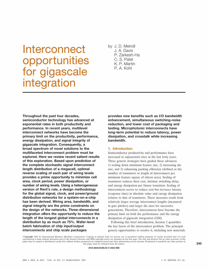
based on results of previous designs. As the number ofwiring levels and the number of repeater circuits increase,via blockage tends to reduce wiring efficiency. The impactof via blockage can be estimated by calculation of a viablockage factor,
BV � AV/Am , (6a)
where AV is the area blocked by vias on a given level ofwiring and Am is the macrocell or chip area. As illustratedin Figure 5(a), terminal vias (which connect a particularinterconnect net to a transistor) cause a “ripple effect”that reduces the number of wiring tracks available in agiven area. In contrast, turn vias (which connect twowiring levels) do not cause via blockage. To elucidatewith a simple example illustrated in Figure 5(a), BV � 0for the five uninterrupted wiring tracks on the left withoutterminal vias, and BV � 0.2 for the four wiring tracks onthe right, where 20% of the available wiring area isblocked by terminal vias [three of which are shown inFigure 5(a)] [12]. Assuming a uniform distribution ofterminal vias as illustrated in Figure 5(b), a generalexpression can be derived for BV in terms of the geometryof the wiring layout [12]:
BV � �NV�2W � s�� 2
Am
, (6b)
where NV is the total number of terminal vias for aparticular metal level on a chip and W, s, and � aredefined in Figure 5(b). The number of terminal vias NV
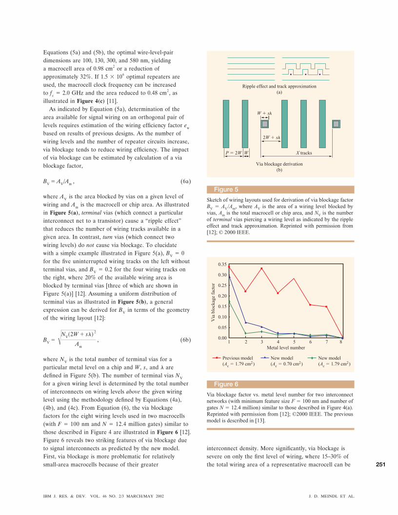
for a given wiring level is determined by the total numberof interconnects on wiring levels above the given wiringlevel using the methodology defined by Equations (4a),(4b), and (4c). From Equation (6), the via blockagefactors for the eight wiring levels used in two macrocells(with F � 100 nm and N � 12.4 million gates) similar tothose described in Figure 4 are illustrated in Figure 6 [12].Figure 6 reveals two striking features of via blockage dueto signal interconnects as predicted by the new model.First, via blockage is more problematic for relativelysmall-area macrocells because of their greater
interconnect density. More significantly, via blockage issevere on only the first level of wiring, where 15–30% ofthe total wiring area of a representative macrocell can be
IBM J. RES. & DEV. VOL. 46 NO. 2/3 MARCH/MAY 2002 J. D. MEINDL ET AL.
251
blocked. The via blockage estimate based on a previousmodel [13] is also illustrated in Figure 6.
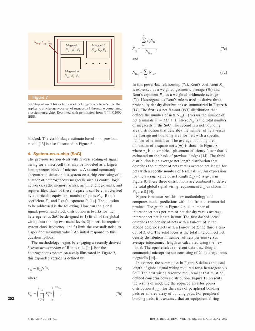
4. System-on-a-chip (SoC)The previous section deals with reverse scaling of signalwiring for a macrocell that may be modeled as a largelyhomogeneous block of microcells. A second commonlyencountered situation is a system-on-a-chip consisting of anumber of heterogeneous megacells such as control logicnetworks, cache memory arrays, arithmetic logic units, andregister files. Each of these megacells can be characterizedby a particular equivalent number of gates NGi , Rent’scoefficient Ki , and Rent’s exponent Pi [14]. The questionto be addressed is the following: How can the globalsignal, power, and clock distribution networks for theheterogeneous SoC be designed to 1) fit all of the globalwiring into the top two metal levels, 2) meet the requiredsystem clock frequency, and 3) limit the crosstalk noise toa specified maximum value? An initial response to thisquestion follows.
The methodology begins by engaging a recently derivedheterogeneous version of Rent’s rule [14]. For theheterogeneous system-on-a-chip illustrated in Figure 7,this expanded version is defined by
Teq � KeqNPeq, (7a)
where
Keq � �i�1
n
KiNGi
1/NGeq
, (7b)
Peq �
�i�1
n
Pi NGi
NGeq
, (7c)
and
NGeq� �
i�1
n
NGi . (7d)
In this power-law relationship (7a), Rent’s coefficient Keq
is expressed as a weighted geometric average (7b) andRent’s exponent Peq as a weighted arithmetic average(7c). Heterogeneous Rent’s rule is used to derive threeprobability density distributions as summarized in Figure 8[14]. The first is a net fan-out (FO) distribution thatdefines the number of nets NNet(m) versus the number ofnet terminals m � FO � 1, where Nm is the total numberof megacells in the SoC. The second is a net boundingarea distribution that describes the number of nets versusthe average net bounding area for nets with a specificnumber of terminals m. The average bounding areadimension of a square net a(m) is shown in Figure 8,where �p is an empirical placement efficiency factor that isestimated on the basis of previous designs [14]. The thirddistribution is an average net length distribution thatdescribes the number of nets versus average net length fornets with a specific number of terminals m. An expressionfor the average value of net length Lav(m) is given inFigure 8. These three distributions are combined to derivethe total global signal wiring requirement Ltot as shown inFigure 8 [14].
Figure 9 summarizes this new methodology andcompares model predictions with data from a commercialproduct. The graph in Figure 9 plots number ofinterconnect nets per mm or net density versus averageinterconnect net length in mm. The first dashed locusdescribes the density of nets with a fan-out of 1; thesecond describes nets with a fan-out of 2; the third a fan-out of 3, etc. The solid locus is the total interconnect netdensity distribution in number of nets per mm versusaverage interconnect length as calculated using the newmodel. The open circles represent data describing acommercial microprocessor consisting of 20 heterogeneousmegacells [14].
In essence, the summation in Figure 8 defines the totallength of global signal wiring required for a heterogeneousSoC. The next wiring resource requirement that must bedefined concerns power distribution. Figure 10 presentsthe results of modeling the required area for powerdistribution Apower, for the cases of peripheral bondingpads or an area array of bonding pads. For peripheralbonding pads, it is assumed that an equipotential ring
J. D. MEINDL ET AL. IBM J. RES. & DEV. VOL. 46 NO. 2/3 MARCH/MAY 2002
252
surrounds the chip, as illustrated in Figure 10(a). For areaarray bonding pads, illustrated in Figure 10(b), it isassumed that Vdd is the potential of each bonding pad andthat the current drain at each orthogonal intersection ofthe power grid lines is constant. ASoC is the total SoC area[14]. In Figure 10, � � �Vdd/Vdd is the normalized voltagedrop from a bonding pad to the most distant via at the
intersection of an orthogonal pair of power grid lines, Vdd
is supply voltage, H is metal height, Ptot is total chip powerdissipation, and W is metal resistivity. Note that APower forarea array bonding pads can be reduced effectively byincreasing the number of bonding pads, npad.
The most critical clock distribution network requirementthat must be met is imposed by the bandwidth necessary
IBM J. RES. & DEV. VOL. 46 NO. 2/3 MARCH/MAY 2002 J. D. MEINDL ET AL.
253
for rapid transitions of the clock waveform. It is assumedthat global clock distribution is implemented with abalanced H-array. This array is modeled as a distributedRC network whose maximum length extends from the chipclock input pad to a terminal buffer/repeater of the globalH-array. The approximate value of this maximum length isthe dimension of the chip edge l. Figure 11 defines theclock frequency limit fClock as a function of chip areaASoC � l 2 [14].
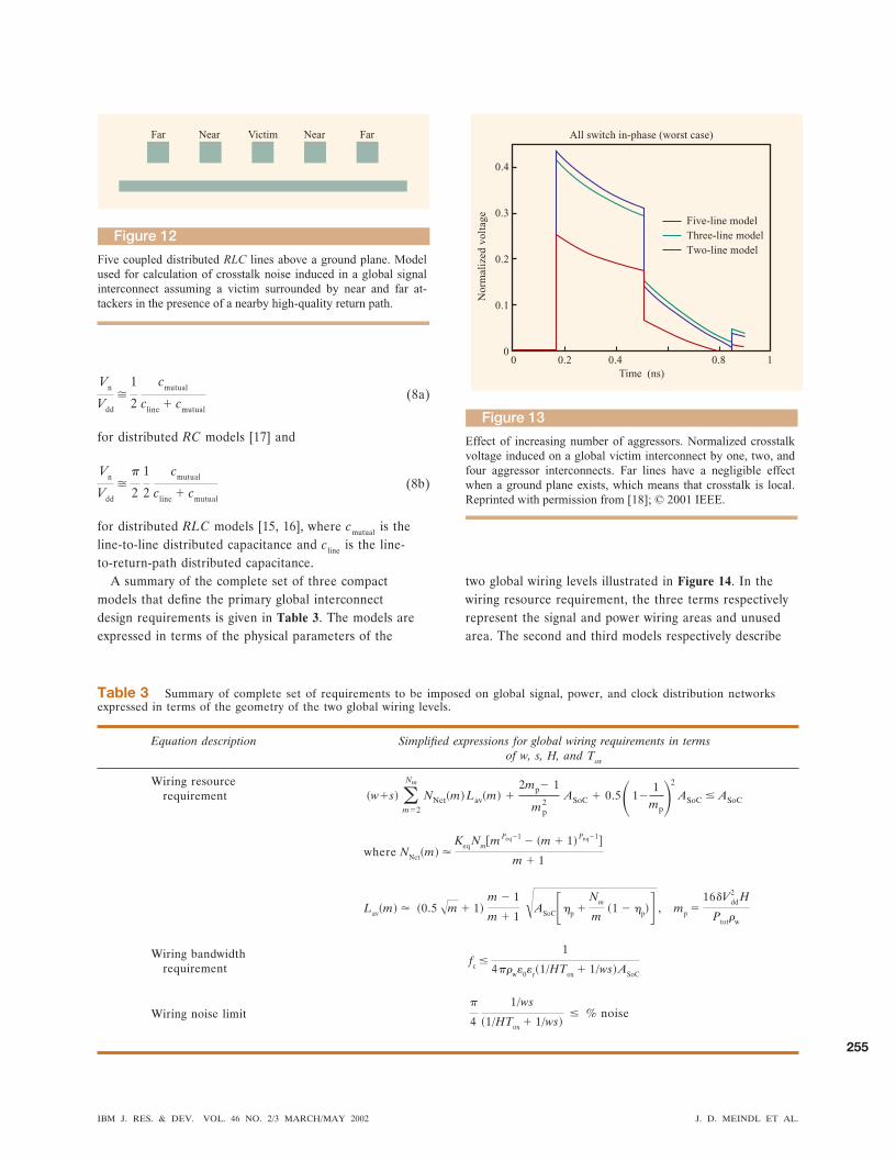
The final performance requirement that is imposed onthe global wiring network is a crosstalk noise limit. A
model used for an approximate calculation of globalcrosstalk noise is illustrated in Figure 12. In thisrepresentation, a global signal line or “victim” is assumedto be surrounded by two near and two far “attackers.”Simultaneous in-phase switching of the four attackerscauses crosstalk noise on the victim due to coupling ofboth mutual capacitance and mutual inductance. A nearbyhigh-quality return path is assumed to be available.Treating the five coupled lines as distributed RLCnetworks, a set of partial differential equations quantifiesthe problem [15, 16]. Some results of a solution to this setof equations are illustrated in Figure 13, which plots theratio of crosstalk-to-binary signal voltage swing versus time[16]. Comparing the three- and five-line loci, it is evidentthat in the presence of a nearby high-quality return path,the near attackers shield the victim from the far attackers.Therefore, using the three-line model, simplifiedexpressions for peak crosstalk voltage derived from thesolutions of the set of partial differential equations are
Figure 10
APower = ASoC
2ma � 1
ma
ma 16 Vdd
Hnpad
Ptot w
2
2�
Pad pitch
�Vdd
(b)
APower = ASoC
2mp � 1
mp
mp 16 Vdd
H
Ptot w
2
2�
�Vdd
(a)
Summary of power wiring area (Apower) derivation for (a) peripheral bonding pads and (b) area array bonding pads as a function of chip or macrocell area ASoC. � � IR/V
dd � �V
dd/V
dd,
where Vdd
is supply voltage; H is metal height, Ptot
is total chip power dissipation,
w is wire resistivity, and n
pad is the number of
power-supply pads.
Figure 11
Summary of global H-array clock distribution network bandwidth requirements f
–3dB and limit on clock frequency f
Clock for a
distributed RC network model of the H-array.
Atte
nuat
ion
(dB
)
An interconnect can be modeled as a low-pass filter.
J. D. MEINDL ET AL. IBM J. RES. & DEV. VOL. 46 NO. 2/3 MARCH/MAY 2002
254
Vn
Vdd
�1
2
cmutual
cline � cmutual
(8a)
for distributed RC models [17] and
Vn
Vdd
��
2
1
2
cmutual
cline � cmutual
(8b)
for distributed RLC models [15, 16], where cmutual is theline-to-line distributed capacitance and c line is the line-to-return-path distributed capacitance.
A summary of the complete set of three compactmodels that define the primary global interconnectdesign requirements is given in Table 3. The models areexpressed in terms of the physical parameters of the
two global wiring levels illustrated in Figure 14. In thewiring resource requirement, the three terms respectivelyrepresent the signal and power wiring areas and unusedarea. The second and third models respectively describe
Figure 12
Five coupled distributed RLC lines above a ground plane. Model used for calculation of crosstalk noise induced in a global signal interconnect assuming a victim surrounded by near and far at-tackers in the presence of a nearby high-quality return path.
Table 3 Summary of complete set of requirements to be imposed on global signal, power, and clock distribution networksexpressed in terms of the geometry of the two global wiring levels.
Equation description Simplified expressions for global wiring requirements in termsof w, s, H, and Tox
Wiring resourcerequirement �w�s�
m�2
Nm
NNet�m� Lav�m� �2mp 1
mp2
ASoC � 0.5� 11
mp�2
ASoC � ASoC
where NNet�m� �Keq Nm�m Peq1
� �m � 1� Peq1�
m � 1
Lav�m� � �0.5�m � 1�m � 1
m � 1�ASoC��p �
Nm
m�1 � �p�� , mp �
16�Vdd2 H
Ptotw
Wiring bandwidthrequirement
fc �1
4�w�0�r�1/HTox � 1/ws� ASoC
Wiring noise limit�
4
1/ws
�1/HTox � 1/ws�� % noise
IBM J. RES. & DEV. VOL. 46 NO. 2/3 MARCH/MAY 2002 J. D. MEINDL ET AL.
255
the clock wiring bandwidth and signal wiring crosstalknoise limit. In Figure 15, the three models are applied toa particular SoC consisting of 20 heterogeneous megacellscontaining a total of approximately six million transistors[14]. In the global interconnect design plane, the verticalaxis represents interconnect thickness H and the horizontalaxis, interconnect width W. The allowable design region thatsatisfies all primary global wiring requirements is the zonebounded by the resource, bandwidth, and noise limit loci.For example, an interconnect width W � 2.4 �m andheight H � 2.0 �m satisfies the prime design constraintswith a minimum pitch. Projections of the allowable design
regions for several future generations of technology areillustrated in Figure 16. Here it is evident that the amountof compression of the allowable design region becomesunacceptable, and additional flexibility such as expansionof the number of global wiring levels appears to becomenecessary.
In summary, the methodology presented in this sectionenables early projections of key physical parameters of aglobal interconnect network that simultaneously satisfiesthe primary requirements of a SoC for signal, power, andclock distribution. The compact physical models thatserve to implement the methodology offer a convenientopportunity to establish a quantitative guide to detaileddesign of a SoC. Therefore, the methodology may serve asa useful precursor to final design. Enhancements of thismethodology that include, for example, the effects of clockskew, nonideal return paths, and simultaneous switchingnoise are needed.
5. Three-dimensional integrationAchieving three-dimensional (3D) integration insemiconductor technology requires the capability tostack multiple strata, each containing both transistorsand multilevel interconnect networks, as discussedin preceding sections. This is a formidable challengethat is unlikely to be engaged seriously absent aconvincing case for substantive benefits. Therefore,what are the primary benefits that can be projectedfor 3D integration? It appears that the singular genericadvantage of 3D integration is a substantial reductionin length of the longest global interconnects used ina SoC.
Several rigorous derivations of stochastic interconnectdistributions for 3D random logic networks [18 –20] basedupon the 2D distribution discussed in Section 3 [7, 8] havebeen reported. Using the analytic models derived in [20],the stochastic interconnect distributions for a 4.0-million-gate random logic network implemented with 1, 4, and16 strata are illustrated in Figure 17(a). Note that forsimplicity these distributions assume that the interstratalpitch r � 1, which strictly imposes the condition that theinterstratal pitch equals the intrastratal logic gate pitch.The loci of Figure 17(a) clearly indicate that multiplestrata or 3D integration exerts very little impact on thedensity of local interconnects, but it has a profound effecton the length of the longest interconnects of the logicnetwork. This observation is illustrated with greater clarityin Figure 17(b). The right vertical axis indicates a lengthof approximately 4000 gate pitches for a corner-to-cornerinterconnect in a single-stratum implementation, 2000 gatepitches for a four-stratum implementation, and 1000 gatepitches for a 16-stratum implementation. For time-of-flight-limited global interconnects, this could resultin a 4:1 reduction of latency and the possibility of an
Figure 14
Physical representation of orthogonal interconnect system.
J. D. MEINDL ET AL. IBM J. RES. & DEV. VOL. 46 NO. 2/3 MARCH/MAY 2002
256
approximately fourfold increase in global clock frequency—for the expense of a 16-stratum implementation of thesystem.
A key simplifying assumption limiting the projectionsillustrated in Figures 17(a) and 17(b) is that theinterstratal pitch equals the intrastratal gate pitch, orr � 1. Setting aside this assumption, a generic 3D wiringdistribution for a 4.0-million-gate random logic networkwhose interstratal pitch is treated as an independentvariable has been rigorously derived [20]. Figure 17(c)illustrates a key result of this new derivation forinterstratal pitches r � 1 and r � 50. The twodistributions are quite similar for short local and longglobal interconnect lengths. The only region in which thetwo loci deviate is the midrange of interconnect lengths,where interconnect length and stratal pitch are roughlyequal. Consequently, it appears that interstratal separationdistance is not a critical parameter in determining 3Dwiring distributions.
The generic benefit of substantial reductions in lengthof the longest global interconnects in a distributionresulting from 3D integration is an inherent advantage of3D wiring. A concomitant inherent disadvantage of 3Dstructures is heat removal [21]. Beyond these generalissues, the attraction of 3D integration for specificapplications may be dominated by the peculiar features ofthe application itself. For example, two-dimensional sensor
arrays that require direct access to each sensor cell forimmediate signal preprocessing are interesting prospectsfor 3D integration [22]. More broadly, the capacity toexplore opportunities for extraordinary performanceenhancements through 3D integration would benefit fromgeneric advances in capabilities to fabricate 3D structures.
Figure 16
Global interconnect design plane projections illustrating com-pression of allowable design region and consequently the necessi-ty for greater flexibility such as expansion of the number of wiring levels.
0 1 2 3 4 5
Line width, W ( m)
Key parameters used for the technologygenerations [1].
Technology fc Vdd Ptot Ng generation (MHz) (V) (W) (gates)
IBM J. RES. & DEV. VOL. 46 NO. 2/3 MARCH/MAY 2002 J. D. MEINDL ET AL.
257
6. Input/output interconnect enhancementsThe intent of input/output interconnect enhancements isto improve the cost, size, reliability, and performanceof a gigascale SoC. Historically, bonding wires havebeen the dominant approach to chip input/output (I/O)interconnects [23]. IBM pioneered the introduction ofsolder-bump I/O interconnects using flip-chip technologywith a thin layer of glass passivation sealing the chipencapsulated in silicone gel, which prevented theformation of continuous water films [24, 25]. A particularnovel technology that is currently under investigation forI/O enhancements is described as Sea of Leads (SoL) [26].This technology proposes the use of wafer-level batchfabrication of compliant polymer packages, ultrahigh-density (�104/cm2) x–y–z flexible metal leads, and solder-like bumps attached to the lead tips, as illustrated inFigure 18(a). A short sequence of full-wafer SoL batch-fabrication processes constituting a “tail-end-of-the-line”(TEOL) are envisaged to follow conventional back-end-of-the-line (BEOL) wafer processing. The further intent ofSoL technology is to complete all final electrical testing
and burn-in operations prior to wafer dicing that yieldsknown good packaged die ready for immediate shipmentto customers. The flexible leads are designed to providesufficient x–y–z compliance to accommodate typicaldifferences in the thermal coefficients of expansionbetween a silicon chip and the substrate to which itis attached. The need for epoxy underfill is therebyprecluded, and the possibility of convenient detachmentof a chip from a substrate module is enabled.
Concurrent fabrication of packages and leads of allchips on a wafer extends the historically potent economiesof wafer-level batch processing to the relatively costly die-by-die assembly, bonding, packaging, testing, and burn-inoperations [27, 28]. Moreover, the size of the SoL packageis the minimum for a chip-scale package (CSP). Significantreliability improvement may result from avoidance ofepoxy underfill often needed to relieve stress on relativelyrigid solder-ball connections between chip and substrate.Figure 18(b) is a photomicrograph of an SoL. The circularpattern is the via linking a die-bonding pad with the leaditself, which is the “question-mark-shaped” copper pattern.
J. D. MEINDL ET AL. IBM J. RES. & DEV. VOL. 46 NO. 2/3 MARCH/MAY 2002
258
This peculiar shape is designed to provide a high degreeof x–y axis flexibility and thus accommodate chip–substratethermal expansion differences. The somewhat roundedregion beneath the copper lead defines the boundariesof a polymer interposer air cavity that is introduced toenhance z-axis compliance. This compliance is added inorder to provide convenient and reliable temporaryelectrical contacts between an array of electrical testprobes and the leads of the dice under test, especiallywhen the probe tips are not in a precisely planararrangement. A photomicrograph of the cross sectionof an air cavity is shown in Figure 18(c). An SEM ofa 1 1-cm die with an SoL density of 12 000 per cm2 isshown in Figure 18(d). The leads are oriented along thecontours of expansion of the die to provide a higherdegree of compliance proceeding radially outwardfrom the center to the edge of the die.
Key performance enhancements that appear to be in theoffing for SoL technology include the following [16, 26]:
1. Substantially increased input/output bandwidth for achip resulting from the significantly larger (e.g., �10)number of signal leads that are available.
2. “Time-of-flight” global signal interconnect latency for achip resulting from exiting and then reentering the dieusing external on-module wiring, or “exterconnects,”to implement very-low-loss time-of-flight internalglobal wiring links for the chip.
3. Reduced global clock skew due to use of time-of-flightexterconnects to implement global clock trees.
4. Reduced global clock power dissipation throughrecycling the energy of reflected clock pulsesdistributed through low-loss exterconnects [29].
5. Suppression of far-attacker crosstalk noise on globalsignal interconnects through the use of exterconnectswith nearby high-quality return paths provided bymodule power and ground planes.
6. Suppression of simultaneous switching noise (SSN) andreduced parasitic IR voltage drop in the power/grounddistribution networks resulting from the significantlylarger (e.g., �10) number of power and ground leadsthat are available.
7. Improved isolation and reduced interference inmixed-signal systems resulting from use of separatepower/ground input/output leads for analog and digitalsignals.
Additional opportunities that are available through SoLinclude the capacity to satisfy the voracious appetiteof 3D integration for I/O capacity and the potential forcompatibility of electrical, rf wireless, and photonic I/Ointerconnects.
In short, SoL can be described as a “disruptive”technology, because the intent is to use batch-fabricatedultrahigh-density input/output leads to improve the cost,size, reliability, and performance of an SoC [16, 26].
7. Photonic interconnectsAn exposition of interconnect opportunities for GSI wouldnot be complete without consideration of photonic oroptical interconnects [30 –33]. In order to be competitivewith electrical interconnects for GSI, photonics mustprovide small, low-power, high-speed, low-cost photonemitters, detectors, and conductors or waveguides that arecompatible with CMOS technology. Consequently, thissection focuses on compatible photonics, or photonictechnologies with the long-range potential to satisfy theextremely stringent and particular demands of GSI.
The most challenging objective for CMOS-compatiblephotonic interconnects is an efficient room-temperaturesilicon light emitter. A novel silicon diode which exploitsdislocation loops to introduce a local strain field thatmodifies the band structure to confine carriers near thejunction and therefore enhance light emission was recentlydemonstrated [34].
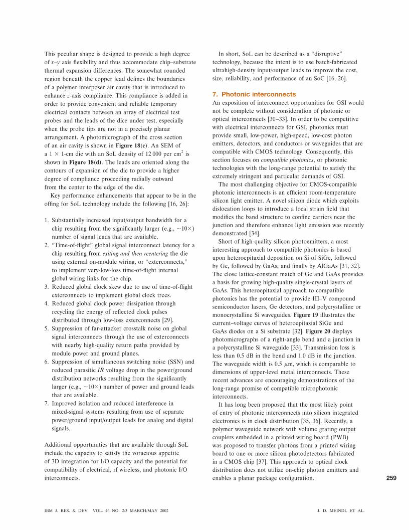
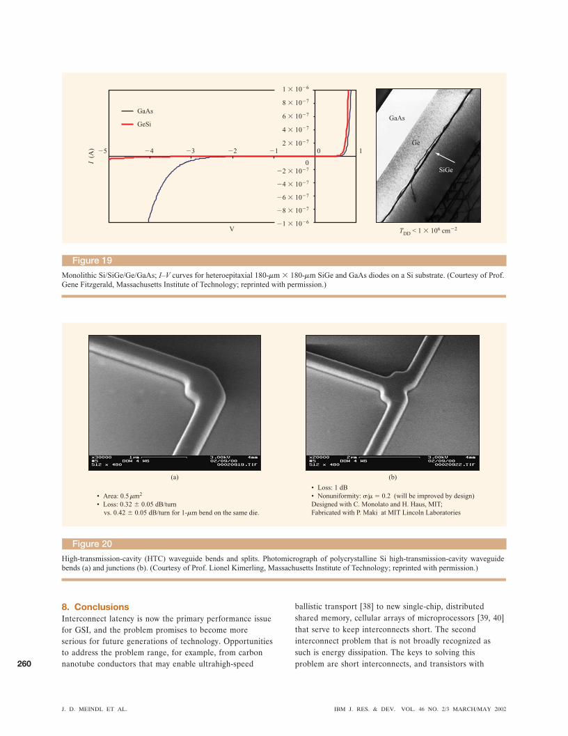
Short of high-quality silicon photoemitters, a mostinteresting approach to compatible photonics is basedupon heteroepitaxial deposition on Si of SiGe, followedby Ge, followed by GaAs, and finally by AlGaAs [31, 32].The close lattice-constant match of Ge and GaAs providesa basis for growing high-quality single-crystal layers ofGaAs. This heteroepitaxial approach to compatiblephotonics has the potential to provide III–V compoundsemiconductor lasers, Ge detectors, and polycrystalline ormonocrystalline Si waveguides. Figure 19 illustrates thecurrent–voltage curves of heteroepitaxial SiGe andGaAs diodes on a Si substrate [32]. Figure 20 displaysphotomicrographs of a right-angle bend and a junction ina polycrystalline Si waveguide [33]. Transmission loss isless than 0.5 dB in the bend and 1.0 dB in the junction.The waveguide width is 0.5 �m, which is comparable todimensions of upper-level metal interconnects. Theserecent advances are encouraging demonstrations of thelong-range promise of compatible microphotonicinterconnects.
It has long been proposed that the most likely pointof entry of photonic interconnects into silicon integratedelectronics is in clock distribution [35, 36]. Recently, apolymer waveguide network with volume grating outputcouplers embedded in a printed wiring board (PWB)was proposed to transfer photons from a printed wiringboard to one or more silicon photodetectors fabricatedin a CMOS chip [37]. This approach to optical clockdistribution does not utilize on-chip photon emitters andenables a planar package configuration.
IBM J. RES. & DEV. VOL. 46 NO. 2/3 MARCH/MAY 2002 J. D. MEINDL ET AL.
259
8. ConclusionsInterconnect latency is now the primary performance issuefor GSI, and the problem promises to become moreserious for future generations of technology. Opportunitiesto address the problem range, for example, from carbonnanotube conductors that may enable ultrahigh-speed
ballistic transport [38] to new single-chip, distributedshared memory, cellular arrays of microprocessors [39, 40]that serve to keep interconnects short. The secondinterconnect problem that is not broadly recognized assuch is energy dissipation. The keys to solving thisproblem are short interconnects, and transistors with
Figure 20
High-transmission-cavity (HTC) waveguide bends and splits. Photomicrograph of polycrystalline Si high-transmission-cavity waveguide bends (a) and junctions (b). (Courtesy of Prof. Lionel Kimerling, Massachusetts Institute of Technology; reprinted with permission.)
• Area: 0.5 m2
• Loss: 0.32 � 0.05 dB/turn vs. 0.42 � 0.05 dB/turn for 1- m bend on the same die.
• Loss: 1 dB • Nonuniformity: �� � 0.2 (will be improved by design)Designed with C. Monolato and H. Haus, MIT;Fabricated with P. Maki at MIT Lincoln Laboratories�
� �
(a) (b)
Figure 19
SiGe
Monolithic Si/SiGe/Ge/GaAs; I–V curves for heteroepitaxial 180- m � 180- m SiGe and GaAs diodes on a Si substrate. (Courtesy of Prof. Gene Fitzgerald, Massachusetts Institute of Technology; reprinted with permission.)
1 � 10�6
8 � 10�7
6 � 10�7
4 � 10�7
2 � 10�7
0�2 � 10�7
�4 � 10�7
�6 � 10�7
�8 � 10�7
�1 � 10�6
�5 �4 �3 �2 �1 0 1
V
GaAs
GeSi
TDD < 1 � 106 cm�2
I (
A)
� �
GaAs
Ge
J. D. MEINDL ET AL. IBM J. RES. & DEV. VOL. 46 NO. 2/3 MARCH/MAY 2002
260
the smallest possible subthreshold swing and thereforethe smallest possible binary signal swing. Crosstalkand simultaneous switching noise represent a thirdinterconnect problem—signal integrity—which is difficultto describe using compact physical models.
For virtually any family of gigascale chips, the key tooptimal reverse scaling of multilevel signal interconnectnetworks is prediction of the complete stochastic wiringdistribution of a next-generation product. More generalsignal integrity models that can be incorporated intoreverse scaling methodologies are needed.
The task of conjointly optimizing the architecture ofthe global signal, clock, and power/ground distributionnetworks of a system-on-a-chip consisting of a set ofheterogeneous megacells is demanding. A first attemptto address this task comprehensively engages a newstochastic model for global signal wiring, a new modelfor global power/ground wiring area, a global clockbandwidth requirement, and a crosstalk noise requirement.Enhancements of current methodologies that include, forexample, the effects of clock skew, nonideal return paths,and simultaneous switching noise are needed.
The generic benefit of substantial reductions (e.g.,�50%) in the length of the longest global interconnects ina distribution is an inherent advantage of 3D integration.The capacity to explore novel opportunities forextraordinary performance enhancements through 3Dintegration would benefit from generic advances incapabilities to fabricate 3D structures.
In order to maintain historic rates of advance ofmonolithic semiconductor technology, more attentionto ancillary features and particularly to input/outputinterconnects is unavoidable. Sea of Leads representsan early effort to more intimately couple the chip itselfto its environment and then to exploit concomitant newopportunities. Key projected performance enhancementsinclude substantially increased input/output bandwidth,reduced global signal interconnect latency, reduced globalclock skew, reduced global clock power dissipation,greater suppression of simultaneous switching noise, andimproved signal integrity in mixed-signal systems. Morebroadly, Sea of Leads represents an effort to extend thequintessential feature of semiconductor technology—wafer-level batch fabrication of several hundred chips—tothe traditional die-by-die packaging and testing domains.
To be become widely used in GSI, photonics mustprovide small, low-power, high-speed, low-cost photonemitters, detectors, and conductors or waveguides thatare compatible with CMOS technology [41]. Recentadvances in heteroepitaxial deposition on Si of SiGe,followed by Ge, followed by GaAs to demonstratelight-emitting and -detecting diodes as well as Siwaveguides, are promising.
AcknowledgmentsThe intellectual contributions to this paper by AzadNaeemi, Raguraman Venkatesan, Muhannad Bakir, HirenThacker, Qiang Chen, James Joyner, and Tony Mule ofthe Georgia Institute of Technology MicroelectronicsResearch Center are gratefully acknowledged. In addition,the authors wish to express their appreciation to DARPA,Contract No. F33615-97-C-1132, MARCO, Contract No.MDA 972-99-1-002, and the SRC, Contract No. 448:048,for their generous support.
References1. J. D. Meindl, “Low Power Microelectronics: Retrospect
and Prospect,” Proc. IEEE 83, 619 – 635 (April 1995).2. M. Bohr, S. S. Ahmed, S. U. Ahmed, M. Bost, T. Ghani,
J. Greason, R. Hainsey, C. Jan, P. Packan, S. Sivakumar,S. Thompson, J. Tsai, and S. Yang, “A High Performance0.25 Micron Logic Technology Optimized for 1.8VOperation,” IEDM Tech. Digest, pp. 847– 850 (December1996).
3. International Technology Roadmap for Semiconductors(ITRS), 1999 Edition, Semiconductor IndustryAssociation, 4300 Stevens Suite Boulevard, Suite 271,San Jose, CA 95129.
4. T. N. Theis, “The Future of Interconnection Technology,”IBM J. Res. & Dev. 44, 379 –390 (May 2000).
5. J. Hennessy, M. Heinrich, and A. Gupta, “Cache-Coherent Distributed Shared Memory: Perspectives inIts Development and Future Challenges,” Proc. IEEE87, 418 – 429 (March 1999).
6. B. Landman and R. Russo, “On a Pin Versus BlockRelationship for Partition of Logic Paths,” IEEE Trans.Computing C-20, 1469 –1479 (December 1971).
7. J. A. Davis, V. K. De, and J. D. Meindl, “A StochasticWire-Length Distribution for Gigascale Integration(GSI)—Part I: Derivation and Validation,” IEEE Trans.Electron Devices 45, 580 –589 (March 1998).
8. J. A. Davis, V. K. De, and J. D. Meindl, “A StochasticWire-Length Distribution for Gigascale Integration(GSI)—Part II: Applications to Clock Frequency, PowerDissipation, and Chip Size Estimation,” IEEE Trans.Electron Devices 45, 590 –597 (March 1998).
9. R. Venkatesan, J. A. Davis, K. A. Bowman, and J. D.Meindl, “Minimum Power and Area N-Tier MultilevelInterconnect Architectures Using Optimal RepeaterInsertion,” Proceedings of the International Symposium onLow Power Electronics and Design (ISLPED), July 2000,pp. 167–172.
10. H. B. Bakoglu and J. D. Meindl, “Optimal InterconnectCircuits for VLSI,” IEEE Trans. Electron Devices ED-32,903–909 (May 1985).
11. H. B. Bakoglu and J. D. Meindl, “Optimal InterconnectCircuits for VLSI,” ISSCC Digest of Technical Papers,February 1984, pp. 164 –165.
12. Q. Chen, J. A. Davis, P. Zarkesh-Ha, and J. D. Meindl,“A Compact Physical Via Blockage Model,” IEEE Trans.Very Large Scale Integration (VLSI) Syst. 8, 689 – 692(December 2000).
13. G. A. Sai-Halasz, “Performance Trends in High-EndProcessors,” Proc. IEEE 83, 20 –36 (January 1995).
14. P. Zarkesh-Ha, J. A. Davis, and J. D. Meindl, “Predictionof Net-Length Distribution for Global Interconnects in aHeterogeneous System-on-a-Chip,” IEEE Trans. VeryLarge Scale Integration (VLSI) Syst. 8, 649 – 659 (December2000).
15. (a) J. Davis and J. D. Meindl, “Compact Distributed RLCInterconnect Models Part I: Single Line Transient, Time
IBM J. RES. & DEV. VOL. 46 NO. 2/3 MARCH/MAY 2002 J. D. MEINDL ET AL.
261
Delay, and Overshoot Expressions,” IEEE Trans. ElectronDevices 45, 580 –589 (November 2000). (b) J. Davis andJ. D. Meindl, “Compact Distributed RLC InterconnectModels Part II: Coupled Line Transient Expressions andPeak Crosstalk in Multilevel Networks,” IEEE Trans.Electron Devices 45, 590 –597 (November 2000).
16. A. Naeemi, C. Patel, M. Bakir, P. Zarkesh-Ha, K. Martin,and J. Meindl, “Sea of Leads: A Disruptive Paradigm fora System-on-a-Chip (SoC),” ISSCC Digest of TechnicalPapers, February 2001, pp. 280 –281.
17. T. Sakurai, “Closed-Form Expressions for InterconnectDelay, Coupling, and Crosstalk in VLSIs,” IEEE Trans.Electron Devices 40, 118 –124 (January 1993).
18. A. Naeemi, J. A. Davis, and J. D. Meindl, “AnalyticalModels for Coupled Distributed RLC Lines with Idealand Non-Ideal Return Paths,” IEDM Tech. Digest, pp.689 – 692 (December 2001).
19. P. Zarkesh-Ha and J. D. Meindl, “An IntegratedArchitecture for Global Interconnects in a GigascaleSystem-on-a-Chip (GsoC),” IEEE Symposium on VLSITechnology, Digest of Technical Papers, June 2000, pp.194 –195.
20. A. Rahman, A. Fan, J. Chung, and R. Reif, “Wire-LengthDistribution of Three-Dimensional Integrated Circuits,”Proceedings of the IEEE International InterconnectTechnology Conference, June 1999, pp. 233–235.
21. S. J. Souri and K. C. Saraswat, “Interconnect PerformanceModeling for 3D Integrated Circuits with Multiple SiliconLayers,” Proceedings of the IEEE International InterconnectTechnology Conference, June 1999, pp. 24 –26.
22. J. Joyner, P. Zarkesh-Ha, J. Davis, and J. Meindl, “AThree-Dimensional Stochastic Wire Length Distributionfor Variable Separation of Strata,” Proceedings of theIEEE International Interconnect Technology Conference,June 2000, pp. 132–134.
23. H. B. Bakoglu, Circuits, Interconnects, and Packaging forVLSI, Addison-Wesley Publishing Co., Inc., Reading, MA,1990, Ch. 3.
24. J. Burns, L. McIlrath, C. Keast, C. Lewis, A. Loomis, K.Warner, and P. Wyatt, “Three-Dimensional IntegratedCircuits for Low-Power, High Bandwidth Systems on aChip,” ISSCC Digest of Technical Papers, February 2001,pp. 268 –269.
25. B. L. Gehman, “Bonding Wire MicroelectronicInterconnections,” IEEE Trans. Components, Hybrids,Manuf. Technol. CHMT-3, 375 (September 1980).
26. E. M. Davis, W. E. Harding, R. S. Schwartz, and J. J.Corning, “Solid Logic Technology: Versatile, High-Performance Microelectronics,” IBM J. Res. & Dev. 8,102–114 (April 1964).
27. P. A. Totta and R. P. Sopher, “SLT Device Metallurgyand Its Monolithic Extension,” IBM J. Res. & Dev. 13,226 –238 (May 1969).
28. A. Naeemi, P. Zarkesh-Ha, C. Patel, and J. D. Meindl,“Performance Improvements Using On-Board Wires forOn-Chip Interconnects,” Proceedings of the IEEEConference on Electrical Performance of ElectronicPackaging, 2000, pp. 325–328.
29. C. S. Patel, C. Power, M. Realff, P. A. Kohl, K. P. Martin,and J. D. Meindl, “Low Cost High Density CompliantWafer Level Package,” Proceedings of the InternationalConference on High-Density Interconnect and SystemsPackaging, Denver, April 26 –28, 2000, pp. 262–268.
30. C. S. Patel, M. Realff, S. Merriweather, C. Power, K.Martin, and J. D. Meindl, “Cost Analysis of CompliantWafer Level Packages,” Proceedings of the 50th ElectronicComponents and Technology Conference (ECTC), LasVegas, May 22–24, 2000, pp. 1634 –1639.
31. H. Reed, M. Bakir, C. Patel, K. Martin, J. Meindl, and P.Kohl, “Compliant Wafer Level Package (CWLP) with Air-Gaps for Sea of Leads (SoL) Interconnections,”
Proceedings of the International Interconnect TechnologyConference, San Francisco, June 4 – 6, 2001, pp. 151–153.
32. P. Zarkesh-Ha and J. D. Meindl, “Stochastic Net LengthDistribution for Global Interconnects in a HeterogeneousSystem-on-a-Chip,” Symposium on VLSI Technology,Digest of Technical Papers, June 1998, pp. 44 – 45.
33. A. V. Krishnamoorthy and D. A. B. Miller, “ScalingOptoelectronic-VLSI Circuits into the 21st Century:A Technology Roadmap,” IEEE J. Quantum Electron.2, 55–76 (April 1996).
34. L. M. Giovane, J. Foresi, M. Morse, L. Liao, A. Agarwal,X. Duan, L. Kimerling, J. Michel, A. Thilderkvist, and E.Fitzgerald, “Materials for Monolithic SiliconMicrophotonics,” Proceedings of the Symposium onMaterials Devices for Silicon-Based Optoelectronics,Warrendale, PA, 1998, pp. 45–56.
35. E. A. Fitzgerald and L. C. Kimerling, “Silicon-BasedMicrophotonics and Integrated Optoelectronics,” Mater.Res. Soc. Bull. 23, 4 (April 1998).
36. L. C. Kimerling, “Silicon Microphotonics,” Appl. Surf. Sci.159 –160, 8 –13 (June 2000).
37. W. L. Ng, U. Lourenco, R. Gwilliam, S. Dedain, G. Shao,and K. Homewood, “An Efficient Room-TemperatureSilicon-Based Light-Emitting Diode,” Nature 410, 192–194(March 8, 2001).
38. J. W. Goodman, S. Kung, and R. Ahtale, “OpticalInterconnections for VLSI Systems,” Proc. IEEE 72, 850 –866 (July 1984).
39. S. K. Tewsbury and L. A. Hornak, “Optical ClockDistribution in Electronic Systems,” J. VLSI Signal Proc.16, 225–246 (June–July 1997).
40. A. V. Mule, S. Schultz, E. Glytsis, T. Gaylord, and J.Meindl, “Input Coupling and Guided Wave DistributionSchemes for Broad-Band Intrachip Guided Wave OpticalClock Distribution Networks Using Volume GratingCoupler Technology,” Proceedings of the IEEEInternational Interconnect Technology Conference,June 4 – 6, 2001, pp. 128 –130.
41. C. Zhou, J. Kong, and H. Dai, “Electrical Measurementsof Individual Semiconducting Single-Walled CarbonNanotubes of Various Diameters,” Appl. Phys. Lett. 76,1597–1599 (March 2000).
42. V. Mulutinovic and P. Stenstrom, “Special Issue onDistributed Shared Memory Systems,” Proc. IEEE 87,399 – 403 (March 1999).
43. W. J. Dally and J. W. Poulton, Digital Systems Engineering,Cambridge University Press, New York, 1998.
44. D. A. B. Miller, “Rationale and Challenges for OpticalInterconnects to Electronic Chips,” Proc. IEEE 88, 728 –748 (June 2000).
Received May 22, 2001; accepted for publicationJanuary 7, 2002
J. D. MEINDL ET AL. IBM J. RES. & DEV. VOL. 46 NO. 2/3 MARCH/MAY 2002
262
James D. Meindl Microelectronics Research Center, GeorgiaInstitute of Technology, 791 Atlantic Avenue, NW, Atlanta,Georgia 30332 ([email protected]). Dr. Meindlis the Director of the Joseph M. Pettit MicroelectronicsResearch Center and the Joseph M. Pettit Chair Professorof Microelectronics at the Georgia Institute of Technology.He is also Director of the Interconnect Focus Center,a multi-university research effort managed jointly by theMicroelectronics Advanced Research Corporation and theDefense Advanced Research Projects Agency for DoD. Hiscurrent research interests focus on physical limits on gigascaleintegration. Dr. Meindl is a Life-fellow of IEEE and theAmerican Association for the Advancement of Science, and amember of the American Academy of Arts and Sciences andthe National Academy of Engineering and its AcademicAdvisory Board. He received his bachelor’s, master’s anddoctor’s degrees in electrical engineering from CarnegieInstitute of Technology (Carnegie Mellon University).
Jeffrey A. Davis Microelectronics Research Center, GeorgiaInstitute of Technology, 791 Atlantic Avenue, NW, Atlanta,Georgia 30332 ([email protected]). Dr. Davis received theB.E.E., M.S.E.E., and Ph.D. degrees in electrical engineeringfrom the Georgia Institute of Technology in 1993, 1997, and1999, respectively. He joined the faculty at Georgia Tech asan Assistant Professor in 1999. In June 2000, Dr. Davisreceived the best student paper award for the 1999International Interconnect Technology Conference (IITC) forinterconnect modeling and design exploration of gigascaleintegrated (GSI) systems. In January 2001 he received theNational Science Foundation CAREER Award to explorenovel alternatives to global interconnect design for future GSIsystems. Dr. Davis is currently the general chair of the 2002System Level Interconnect Prediction (SLIP) workshop(www.sliponline.org).
Payman Zarkesh-Ha LSI Logic Corporation,1551 McCarthy Boulevard, Milpitas, California 95035([email protected]). Dr. Zarkesh-Ha is a Research StaffMember in the Interconnect Modeling Group in the DeviceTechnology Division of LSI Logic Corporation. He received aB.S. degree in electrical engineering from the University ofScience and Technology, Tehran, Iran, in 1992, an M.S.degree in electrical engineering from Sharif University,Tehran, Iran, in 1994, and a Ph.D. degree in electricalengineering from the Georgia Institute of Technology,Atlanta, in 2001. He subsequently joined LSI LogicCorporation, where he has worked on interconnectarchitecture design for the next ASIC generations. Heis an author or coauthor of two patents and 25 technicalpapers. Dr. Zarkesh-Ha is a member of the Institute ofElectrical and Electronics Engineers.
Chirag S. Patel IBM Research Division, Thomas J. WatsonResearch Center, P.O. Box 218, Yorktown Heights, New York10598 ([email protected]). Dr. Patel is a Research StaffMember in the Science and Technology Department at theThomas J. Watson Research Center. He received B.S., M.S.,and Ph.D. degrees in electrical engineering from the GeorgiaInstitute of Technology in 1995, 1996 and 2001, respectively.In 2000 Dr. Patel received an outstanding paper award at theHigh Density Interconnect Conference for his work on thecompliant wafer-level package. In 2001, he joined IBM at theThomas J. Watson Research Center, where he has worked onadvanced and exploratory packaging technologies. He is an
author or coauthor of more than 25 technical papers.Dr. Patel is a member of the Institute of Electrical andElectronics Engineers.
Kevin P. Martin Microelectronics Research Center, GeorgiaInstitute of Technology, 791 Atlantic Avenue, NW, Atlanta,Georgia 30332 ([email protected]). Dr. Martin is aSenior Research Scientist in the Microelectronics ResearchCenter at the Georgia Institute of Technology. He receivedhis B.S. degree in 1976, his M.S. degree in 1979, and hisPh.D. degree in 1982, all in physics from Ohio StateUniversity. He has since held research positions at BostonUniversity, the Francis Bitter National Magnet Laboratory atMIT, the University of Oregon, and Georgia Tech (where hehas worked since 1987). His research activities include theinteger and fractional quantum Hall effect, resonant tunnelingin quantum-well nanostructures, physics of compoundsemiconductors, plasma processing of semiconductors,properties of semiconductor nanostructures, nanofabrication,wafer-level packaging, and high-performance ultrahigh-densityinput/output interconnects. Dr. Martin is an author andcoauthor of more than 50 peer-reviewed journal papers andcoinventor of six allowed patents. He has been a member ofthe American Physical Society, the American Vacuum Society,and the Institute of Electrical and Electronics Engineers.
Paul A. Kohl Microelectronics Research Center, GeorgiaInstitute of Technology, 791 Atlantic Avenue, NW, Atlanta,Georgia 30332 ([email protected]). Dr. Kohl receiveda Ph.D. degree from the University of Texas in 1978. Heworked at AT&T Bell Laboratories from 1978 to 1989 in thearea of materials and processes for semiconductor devices.In 1989, he joined the School of Chemical Engineering atthe Georgia Institute of Technology, where he is currentlyRegents’ Professor. His research interests include newmaterials and chemical processes for semiconductor andelectrochemical devices.
IBM J. RES. & DEV. VOL. 46 NO. 2/3 MARCH/MAY 2002 J. D. MEINDL ET AL.