51
THE BITBUSTM INTERCONNECT SERIAL CONTROL BUS SPECIFICATION © Intel Corporation, 1988 Order Number: 280645-001
THE BITBUSTM INTERCONNECT SERIAL CONTROL BUS
SPECIFICATION
© Intel Corporation, 1988 Order Number: 280645-001

In the United States, additional copies of this manual or other Intel literature may be obtained from:
Literature Department Intel Corporation 3065 Bowers Avenue Santa Clara, CA 95051
Intel Corporation makes no warranty of any kind with regard to this material, including, but not limited to, the implied warranties of merchantability and fitness for a particular purpose. Intel Corporation assumes no responsibility for any errors that may appear in this document. Intel Corporation makes no commitment to update nor to keep current the information contained in this document.
Intel Corporation assumes no responsibility fpr the use of any circuitry other than circuitry embodied in an Intel product. No other circuit patent licenses are implied.
Intel software products are copyrighted by and shall remain the property of Intel Corporation. Use, duplication or disclosure is subject to restrictions stated in Intel's Software License Agreement, or in the case of software delivered to the government, in accordance with the software license agreement as defined in FAR 52.227-7013.
No part of this document may be copied or reproduced in any form or by any means without prior written consent of Intel Corporation.
Intel Corporation retains the right to make changes to these specifications at any time, without notice.
Contact your local sales office to obtain the latest specifications before placing your order.
The following are trademarks of Intel Corporation and its afftliates and may be used only to identify Intel products:
Above iLBX Intellink MICROMAINFRAME Ripplemode BITBUS im iOSP MULTIBUS RMX/SO COMMputer iMDDX iPAT MULTICHANNEL RUPI CREDIT iMMX iPDS MULTIMODULE Seamless Data Pipeline Inboard iPSC ONCE SLD ETOX Insite iRMK OpenNET SugarCube FASTPATH Intel iRMX arp UPI Genius inlel iSBC PC BUBBLE VLSiCEL 4 Intel376 iSBX Plug-A-Bubble 376 I
i Intel386 iSDM PROMPr 386 I2ICE intelBOS iSXM Promware 386SX ICE Intel Certified KEPROM QueX 4-SITE iCEL Intelevision Library Manaser QUEST
iCS Inteligent Identifier MAPNET Quick·Erase iDBP Inteligent Programming MCS Quick·Pulse Programming iDiS Intellee Megachassis
Copyright © 1988, Intel Corporation, All Rights Reserved
inter
REV. REVISION HISTORY PRINT DATE
A Original Issue 1184
B Minor Revisions to Original Issue 7/88
inter BITBUSTM Interconnect Specification
1.0 GENERAL
1.1 SCOPE
Connection of dedicated controllers and process 1/0 pOints to a control computer has been a longtime problem. Traditional methods have used a standard parallel bus to interconnect 1/0 expansion boards, which provide the required signal conditioning. In many cases, these buses are satisfactory; however, in many other cases the characteristics of these parallel buses create significant limitations. Electrically, parallel buses limit the number of boards that can be transparently (Le. in the same backplane) added to the system. Mechanical packaging for parallel buses often makes 1/0 cabling cumbersome, due to the close proximity of boards within a backplane. Most importantly, the fixed form factor and bus interface logic requirements of a parallel bus put a lower bound on future system cost reduction, regardless of the advancing capabilities of future VLSI. The BITBUS11I interconnect is a serial control bus specifically designed to address these problems.
The BITBUS interconnect allows up to 250 nodes to be easily interconnected over a physically distributed domain. Distribution capability ranges from 30 meters for the synchronous mode of operation to thousands of meters forthe self clocked mode of operation. The different modes of operation are optimized for a wide range of applications covering the spectrum from high speed servo motor control in robotics, to long distance environmental control. In all cases the BITBUS interconnect is optimized for the high speed transfer of short control messages in a hierarchical system.
The level of specification for the BITBUS interconnect is somewhat different from traditional parallel bus structures. In the past, serial connections have been slow, software intensive, and hard to use. A goal of the BITBUS interconnect is to provide an easy to use, high performance serial interconnect that is transparent to the application programmer. For this purpose, this specification not only defines electrical and data link protocol aspects of the bus, as is typical for parallel buses, but also specifies a message structure and protocol for a multitasking environment, and a set of high level commands for remote I/O access and application task control. This allows standard high level software interfaces to be written, off-loading the application programmer of this complication. More importantly, this high level of specification allows the standard interface to be driven into silicon, further reducing the interface overhead, cost and complexity.
This specification has been prepared for those users intending to design or evaluate products that will be compatible with the BITBUS interconnect. The intent of this specification is to specify the interface requirements only. The implementation of interface logic and software is left to the user.
1.2 DEFINITIONS
System - A set of interconnected elements which achieve a given objective through performing a specific function. In this specification a BITBUS system consists of one master node and from one to 250 slave nodes attached to the same BITBUS interconnect.
Message-Passing - The transfer and control of structured data between two tasks.
Task - An entity which competes for system resources in order to execute a program.
Protocol - The rules by which information is exchanged across an interface.
Operation - The process whereby information is transferred between two elements across an interface.
Interface - A shared boundary between two elements within a system.
Bit-Cell-Time - The time interval required to transfer one bit of data on a s~rialline.
inter BITBUSTM Interconnect Specification
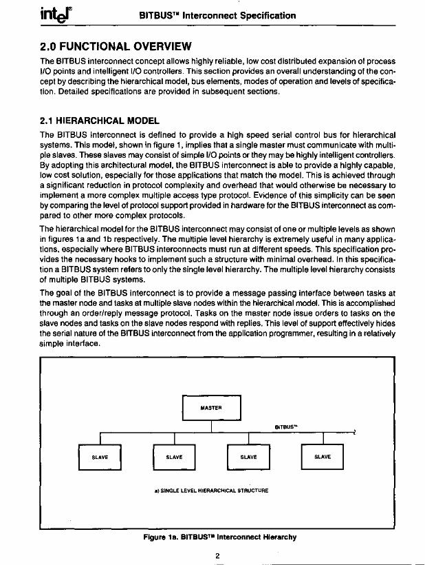
2.0 FUNCTIONAL OVERVIEW The BITBUS interconnect concept allows highly reliable, low cost distributed expansion of process I/O points and intelligent I/O controllers. This section provides an overall understanding of the concept by describing the hierarchical model, bus elements, modes of operation and levels of specification. Detailed specifications are provided in subsequent sections.
2.1 HIERARCHICAL MODEL
The BITBUS interconnect is defined to provide a high speed serial control bus for hierarchical systems. This model, shown in figure 1, implies that a single master must communicate with multi· pie slaves. These slaves may consist of simple I/O points or they may be highly intelligent controllers. By adopting this architectural model, the BITBUS interconnect is able to provide a highly capable, low cost solution, especially for those applications that match the model. This is achieved through a significant reduction in protocol complexity and overhead that would otherwise be necessary to implement a more complex multiple access type protocol. Evidence of this Simplicity can be seen by comparing the level of protocol support provided in hardware for the BITBUS interconnect as compared to other more complex protocols.
The hierarchical model for the BITBUS interconnect may consist of one or multiple levels as shown in figures 1 a and 1 b respectively. The multiple level hierarchy is extremely useful in many applications, especially where BITBUS interconnects must run at different speeds. This specification provides the necessarY hooks to implement such a structure with minimal overhead. In this specification a BITBUS system refers to only the single level hierarchy. The multiple level hierarchy consists of multiple BITBUS systems.
The goal of the BITBUS interconnect is to provide a message passing interface between tasks at the master node and tasks at multiple slave nodes within the hierarchical model. This is accomplished through an order/reply message protocol. Tasks on the master node issue orders to tasks on the slave nodes and tasks on the slave nodes respond with replies. This level of support effectively hides the serial nature of the BITBUS interconnect from the application programmer, resulting in a relatively simple interface.
BITBUS'·
oj SINGLE LEVEL HIERARCHICAL STRUCTURE
Figure 1a. BITBUSTM Interconnect Hierarchy
2
BITBUSTM Interconnect Specification
BITBUS'·
b) MULTIPLE LEVEL HIERARCHICAL STRUCTURE
Figure 1 b. BITBUSTM Interconnect Hierarchy
2.2 BUS ELEMENTS
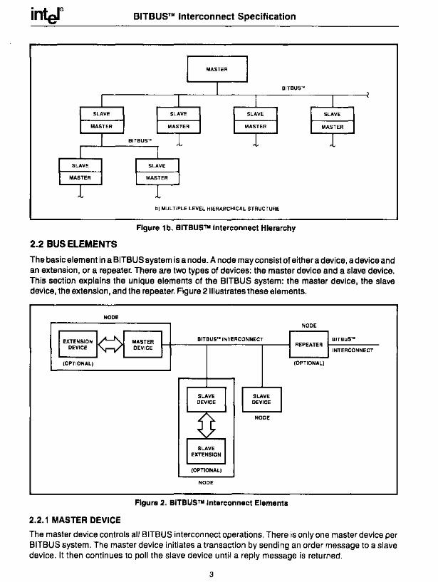
The basic element in a BITBUS system is a node. A node may consist of either a device, a device and an extension, or a repeater. There are two types of devices: the master device and a slave device. This section explains the unique elements of the BITBUS system: the master device, the slave device, the extension, and the repeater. Figure 2 illustrates these elements.
EXTENSION DEVICE
(OPTIONAL)
NODE
2.2.1 MASTER DEVICE
NODE
BITBUS'· INTERCONNECT BITBUS'·
INTERCONNECT
(OPTIONAL)
NODE
Figure 2. BITBUSTM Interconnect Elements
The master device controls all BITBUS interconnect operations. There is only one master device per BITBUS system. The master device initiates a transaction by sending an order message to a slave device. It then continues to poll the slave device until a reply message is returned.
3
inter BITBUS™ Interconnect Specification
During normal operation, each transfer from the master device is acknowledged by the addressed slave device. If a reply is not immediately available, a simple data link acknowledgement is returned. This frees the master device to perform other operations, such as sending another message or polling another slave device. In general, this scheme maximizes the available bus bandwidth within the BITBUS system.
The master device may be stationary in one node or this function may be passed between nodes. Mastership passing in a BITBUS system is performed via a scheme similar to token passing; however, it reduces system reliability (e.g. possibility of lost "tokens") and is therefore in general discouraged. On the other hand, despite the lower reliability, there may be specific cases where passing of mastership is desirable. One example is the implementation of a redundant master. In this case, it may be possible to increase the overall system mean time between failure (MTBF), even with the reduced reliability of passing mastership. This is especially true if all potential masters can be confined to a small section of cable isolated from the rest of the system by a repeater. Note that mastership may not be passed through repeaters.
2.2.2 SLAVE DEVICE
A slave device is a replier in a BITBUS system. There may be up to 250 slaves per system (addresses 1-250). As a replier, the slave may not spontaneously initiate a transfer. Rather, it may only respond to orders from the master device. This approach significantly simplifies the slave device protocol requirements allowing powerful, low cost solutions to be implemented using highly integrated microcontrollers.
2.2.3 EXTENSION
An extension is a secondary processor within a node. The interface between a master or slave device and its extension is not part of this specification. The reason for including the extension in this description is to identify the need for a control field within the standard BITBUS message format to efficiently route messages to a master or slave device or their respective extensions. This allows low cost nodes to be constructed with a single processor and high capability nodes to be constructed with an application processor (extension) and a BITBUS interface processor. By differentiating tasks that run on these two processors, the BITBUS interface processor may contain tasks to off-load the extension processor while the extension processor maintains the capability to send messages directly through to the BITBUS interconnect. This capability may also be used to implement gateways between mUltiple BITBUS systems creating the multiple level hierarchy shown in Figure 1 b.
2.2.4 REPEATERS
A repeater is a node used to regenerate (not reclock) the BITBUS interface signals. Repeaters are used to extend the distance or node count within a BITBUS system. Repeaters are referred to as nodes since they load a segment just as a master or slave node does. Repeaters are only allowed in the self clocked mode of operation. Section 2.3.2 provides more details on repeater operation.
2.3 MODES OF OPERATION
The BITBUS interconnect may operate in one of two modes: synchronous mode or self clocked mode. The purpose for multiple modes is to provide a wide range of performance/distance options for a variety of applications. In this section each mode is presented with its corresponding features and signal line definitions. Note that in both modes of operation all BITBUS interconnect signals are differential. The terminology used to specify the signal pairs is NAME and NAME*. State definition for the signal pairs is provided in section 3.1.1 of this specification.
4
inter BITBUSTM Interconnect Specification
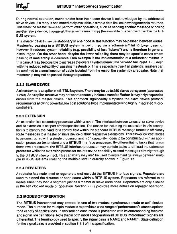
2.3.1 SYNCHRONOUS MODE
The synchronous mode of operation is optimized for the highest performance over a relatively short distance. This mode can interconnect up to 28 nodes over 30 meters at transmission speeds between 500 kbits/sec and 2.4 Mbits/sec. A typical system is shown in figure 3.
DATA CLOCK PAIR " DCLK
DATA PAIR
~I DATA
I I MASTER NODE DATA DCLK DATA DCLK DATA DCLK
SLAVE SLAVE SLAVE NODE 1 NODE 2 NODE 27
Figure 3. Synchronous Mode Connection
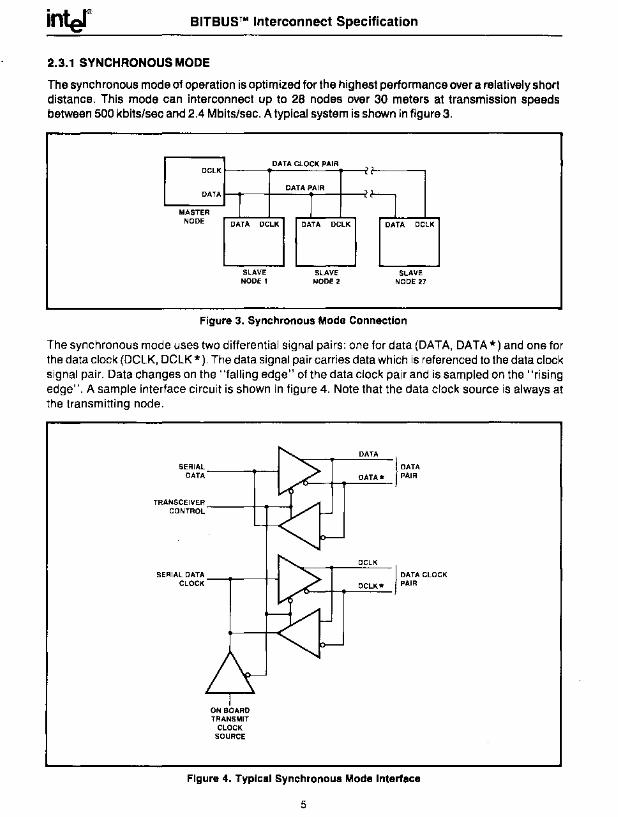
The synchronous mode uses two differential signal pairs: one for data (DATA, DATA *) and one for the data clock (DCLK, DCLK *). The data signal pair carries data which is referenced to the data clock Signal pair. Data changes on the "falling edge" of the data clock pair and is sampled on the "rising edge". A sample interface circuit is shown in figure 4. Note that the data clock source is always at the transmitting node.
SERIA~~~6~ ____ +-I
ON BOARD TRANSMIT
CLOCK SOURCE
DATA
j DATA
DATA * PAIR ~--+----
DCLK
)
DATA CLOCK
A>--+_--=.DC::;L::.;K __ *_ PAIR
Figure 4. Typical Synchronous Mode Interface
5
BITBUSTM Interconnect Specification
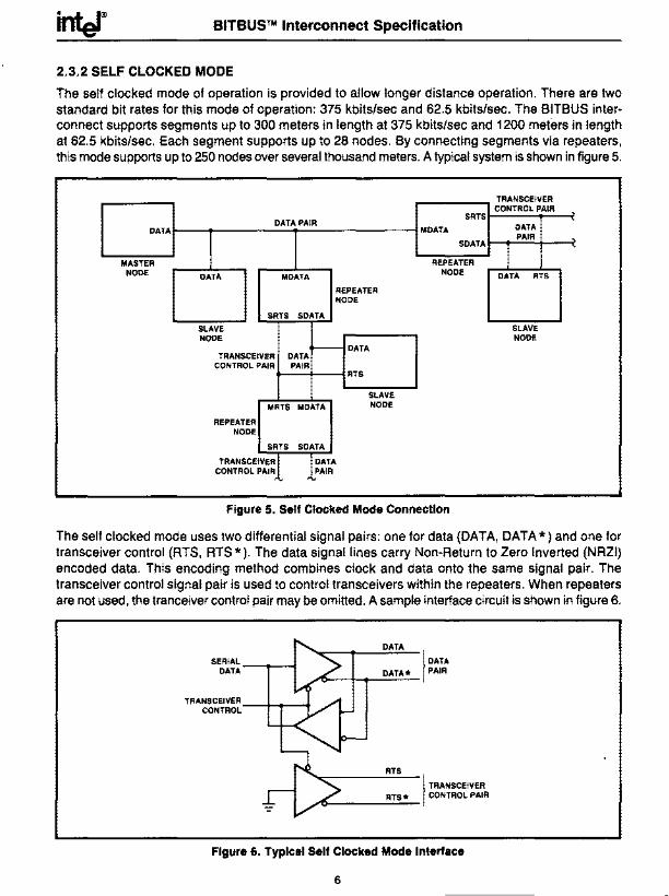
2.3.2 SELF CLOCKED MODE
The self clocked mode of operation is provided to allow longer distance operation. There are two standard bit rates for this mode of operation: 375 kbits/sec and 62.5 kbits/sec. The BITBUS interconnect supports segments up to 300 meters in length at 375 kbits/sec and 1200 meters in length at 62.5 kbits/sec. Each segment supports up to 28 nodes. By connecting segments via repeaters, this mode supports up to 250 nodes over several thousand meters. A typical system is shown in figure 5.
TRANSCEIVER CONTROL PAIR ,
SRTS DATA PAIR DATA DATA MDATA
I I PAIR
SDATA
I ,
MASTER REPEATER NODE DATA MDATA
NODE DATA RTS
REPEATER NODE
SRTS SDATA
SLAVE SLAVE NODE NODE
~ DATA TRANSCEIVER DATA
CONTROL PAIR PAIR RTS
SLAVE
MRTS MDATA NODE
REPEATER NODE
SRTS SDATA
TRANSCEIVE: 1 CONTROL PAIR
lJATA PAIR
Figure 5. Self Clocked Mode Connection
The self clocked mode uses two differential signal pairs: one for data (DATA, DATA *) and one for transceiver control (RTS, RTS *). The data signal lines carry Non-Return to Zero Inverted (NRZI) encoded data. This encoding method combines clock and data onto the same signal pair. The transceiver control signal pair is used to control transceivers within the repeaters. When repeaters are not used, the tranceiver control pair may be omitted. A sample interface circuit is shown in figure 6.
DATA
J
DATA
A>---I_---:D:c..A;.;.;TA-*- PAIR
RTS
J
TRANSCEIVER RTS* CONTROL PAIR ........,:>--__ ......;.0.;..;;....._
Figure 6. Typical Self Clocked Mode Interface
6
inter BITBUSTM Interconnect Specification
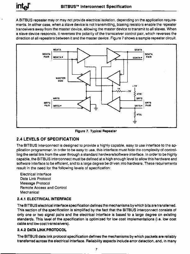
A BITBUS repeater mayor may not provide electrical isolation, depending on the application requirements. In either case, when a slave device is not transmitting, biasing resistors enable the repeater tranceivers away from the master device, allowing the master device to transmit to all slaves. When a slave device responds, it reverses the polarity of the transceiver control pair, which reverses the direction of all repeaters between it and the master device. Figure 7 shows a sample repeater circuit.
MoATA
MoATA I PAIR MoATA*
-----iI--.-<lI
MASTER SIDE
MRTS
MRTS I PAIR MRTS* -------(J ......
"""""'oN\r-+5V
SoATA
I SoATA SoATA* PAIR
+5V
4701l
SRTS
I SRTS SRTS* PAIR
1C>-----1r--
4700
Figure 7. Typical Repeater
2.4 LEVELS OF SPECIFICATION The BITBUS interconnect is designed to provide a highly capable, easy to use interface to the application programmer. In order to be easy to use, this interface must hide the complexity of controlling the serial link from the user through a standard hardware/software interface. In order to be highly capable, the BITBUS interconnect must be defined at a high enough level to allow this hardware and software interface to be efficient, and to a large degree be driven into hardware. These requirements result in the need for the following levels of specification:
Electrical Interface Data Link Protocol Message Protocol Remote Access and Control Mechanical
2.4.1 ELECTRICAL INTERFACE
The BITBUS electrical interface specification defines the mechanisms by which bits are transferred. This section of the specification is simplified by the fact that the BITBUS interconnect consists of only one or two signal pairs and the electrical interface is based to a large degree on existing standards. This level of the specification is optimized for low cost implementations (Le. low cost cable and low cost transceivers).
2.4.2 DATA LINK PROTOCOL
The BITBUS data link protocol specification defines the mechanisms by which packets are reliably transferred across the electrical interface. Reliability aspects include error detection, and, in many
7
inter BITBUS™ Interconnect Specification
cases, error recovery. This is important to the BITBUS interconnect definition since it makes the application less sensitive to the serial nature of the interconnect. This section of the specification is also based to a large degree on existing standards.
2.4.3 MESSAGE PROTOCOL
The BITBUS message protocol specification defines the mechanism by which tasks pas!? messages over the data link. The protocol is optimized for communication between tasks on the master node and tasks on slave nodes. In actual implementations this same protocol can be used to communicate between tasks on the same node as well, allowing the serial bus to appear transparent. The purpose for providing this level in the bus specification is to allow a standard high level user interface to be efficiently implemented, and eventually driven into silicon. This section of the specification is based on a simple high performance protocol, using a well established order/reply mechanism.
2.4.4 REMOTE ACCESS AND CONTROL
The remote access and control (RAC) specification defines a set of high level commands to perform a set of standard operations over the BITBUS interconnect. Remote access commands allow standard 110 operations (e.g. read, write, etc.) to be performed on up to 256110 ports at each slave node without application software. For higher capability systems remote control commands allow slave node tasks to be downloaded, uploaded and controlled from the master device.
2.4.5 MECHANICAL
The BITBUS mechanical specifications are minimal. The purpose for these specifications is to define standard connectors for the BITBUS interconnect and an optional 110 board form factor for higher levels of compatibility.
3.0 ELECTRICAL INTERFACE SPECIFICATION The BITBUS interconnect electrical specification requires definition of data encoding techniques and DC/AC parameters for the interface logic and interconnect cable. This section provides the required definition and specifically points out where existing standards are used as a basis for the specification.
3.1 DATA ENCODING TECHNIQUES
The BITBUS interconnect uses different data encoding techniques for the two modes of operation. Each is discussed separately below, along with a general definition of signal pair state.
3.1.1 GENERAL SIGNAL PAIR STATE DEFINITION
All signals on the BITBUS interconnect are differential pairs. The naming convention for these pairs identifies the two signal lines as NAME and NAME * . An active signal (logical 1 ) is present when the NAME signal line is at a higher electrical potential than the NAME * signal line. An inactive signal (logical 0) is present when the NAME signal line is at a lower electrical potential than the NAME * signal line.
3.1.2 SYNCHRONOUS MODE
Data encoding is relatively simple in the synchronous mode. The logical value of each bit is Simply indicated by the level of the data signal pair at the bit cell center. The bit cell center is defined as the rising edge of the data clock pair. A logical zero is represented by the DATA signal being at a lower electrical potential than the DATA * signal at the bit cell center. A logical one is represented by the DATA signal being at a higher electrical potential than the DATA" signal at the bit cell center. These relationships are shown in figure 8. Data encoding for the synchronous mode of operation
8
BITBUSTM Interconnect Specification
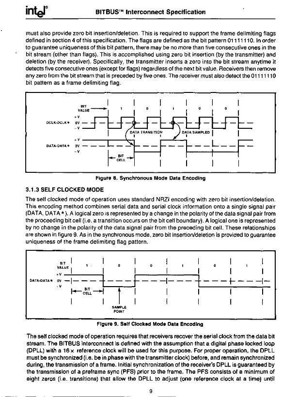
must also provide zero bit insertion/deletion. This is required to support the frame delimiting flags defined in section 4 of this specification. The flags are defined as the bit pattern 01111110. In order to guarantee uniqueness of this bit pattern, there may be no more than five consecutive ones in the bit stream (other than flags). This is accomplished using zero bit insertion (by the transmitter) and deletion (by the receiver). Specifically, the transmitter inserts a zero into the bit stream anytime it detects five consecutive ones (except for flags) regardless of the next bit value. Receivers then remove any zero from the bit stream that is preceded by five ones. The receiver must also detect the 01111110 bit pattern as a frame delimiting flag.
BIT 1 VALUE-I
+V
o o
DCLK·DCLK*
-V
DATA·DATA*
-V
Figure 8. Synchronous Mode Data Encoding
3.1.3 SELF CLOCKED MODE
The self clocked mode of operation uses standard NRZI encoding with zero bit insertion/deletion. This encoding method combines serial data and serial clock information onto a single signal pair (DATA, DATA *). A logical zero is represented by a change in the polarity of the data signal pair from the proceeding bit cell (i.e. a transition occurs on the bit cell boundary). A logical one is represented by no change in the polarity of the data signal pair from the preceding bit cell. These relationships are shown in figure 9. As in the synchronous mode, zero bit insertion/deletion is provided to guarantee uniqueness of the frame delimiting flag pattern.
BIT 1 1 1 0 1 0 1 1 1 0 1 1 1 VALUE 1 1 I I 1 1 1
DATA·DATA* ~~ -1- - --+---f - - -1- - --+- --t- - - -1-I-C~[L -I til 1 1 I
SAMPLE POINT
1 1 1 1
Figure 9. Self Clocked Mode Data Encoding
The self clocked mode of operation requires that receivers recover the serial clock from the data bit stream. The BITBUS interconnect is defined with the assumption that a digital phase locked loop (DPLL) with a 16 x reference clock will be used for this purpose. For proper operation, the DPLL must be synchronized (Le. be in phase with the transmitter clock) before, and remain synchronized during, the transmission of a frame. Initial synchronization of the receiver's DPLL is guaranteed by the transmission of a preframe sync (PFS) prior to the frame. The PFS consists of a minimum of eight zeros (Le. transitions) that allow the DPLL to adjust (one reference clock at a time) until
9
BITBUSTM Interconnect Specification
synchronized. Once synchronized, the DPLL uses the transitions (Le. zeros) within the bit stream to make fine adjustments of ± 1 reference clock cycle. Note that zero bit insertion/deletion guarantees a transition at least every seven bit cells, allowing a reasonable tolerance on the reference clock.
3.2 DC SPECIFICATIONS
The DC specifications for the BITBUS interconnect are based on the RS485 electrical standard. This section defines the characteristics of a standard load, a transmitter, a receiver, the interconnect cable and the terminating and biasing resistors.
3.2.1 STANDARD LOAD SPECIFICATION
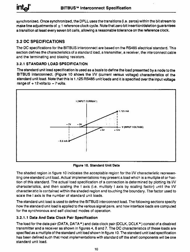
The standard unit load specification is used as a basis to define the load presented by a node to the BITBUS interconnect. (Figure 10 shows the IIV (current versus voltage) characteristics of the standard unit load. Note that this is 1 .125 RS485 unit loads and it is specified over the input voltage range of + 12 volts to - 7 volts.
I (INPUT CURRENT)
------1f--..JoC~--~---of- V (INPUT VOLTAGE)
-0.9 mA
Figure 10. Standard Unit Data
The shaded region in figure 10 indicates the acceptable region for the IN characteristic representing one standard unit load. Actual implementations may present a load which is a multiple of or fraction of this standard. The actual load specification of a connection is determined by plotting its IN characteristics, and then scaling the I axis (Le. multiply I axis by scaling factor) until the IN characteristic is contained within the shaded region and touching the boundary. The factor used to scale the I axis is the number of standard unit loads.
The standard unit load is used to define the BITBUS interconnect load. The following sections specify how the standard unit load is applied to the various signal pairs, and how interface loads are computed for the synchronous and self clocked modes of operation.
3.2.1.1 Data And Data Clock Pair Specification
The load for the data paJr (DATA, DATA *) and data clock pair (DCLK, DCLK *) consist of a disabled transmitter and a receiver as shown in figures 4, 6 and 7. The DC characteristics of these loads are specified as a multiple of the standard unit load shown in figure 10. The standard unit load specification has been defined such that most implementations with standard off the shelf components will be one standard unit load.
10
inter BITBUSTM Interconnect Specification
3.2.1.2 ""anscelver Control Pair Specification
The load for the transceiver pair (RTS, RTS*) is not the same as the data pair. While data may be driven from the master to a slave, as we" as from a slave back to the master, the transceiver signals are driven one direction only-from a slave back towards the master. This difference is shown in Figure 7.
A BITBUS segment may have up to 28 RTS/RTS * transmitters and one RTS/RTS * recei'ler. At any time, no more than one of these transmitter pairs is active. This active transmitter sees one receiver and up to 27 inactive transmitters.
The DC characteristics of the inactive transmitter loads are specified as a multiple of 119 the standard unit load shown in Figure 10. For example, if a transceiver node presents 219 standard unit loads, it is counted as 2 BITBUS interconnect loads. The DC characteristics of the active receiver load shall not exceed 25 standard unit loads, including the biasing resistors specified in section 3.2.5. With this definition, 27 inactive transmitter nodes and one active receiver node are equivalent to 28 standard unit loads (27 x 1/9 + 25 = 28).
3.2.1.3 Synchronous Mode Load
The load presented to the BITBUS interconnect in synchronous mode is defined by determining the number of standard unit loads for each signal pair. The largest number is the specification. For example, if the data signal pair presents a load equal to the standard unit load, and the data clock Signal pair presents a load equal to 2 standard unit loads, the interface would be specified as 2 loads.
3.2.1.4 Self Clocked Mode Load The load presented to the BITBUS interconnect in the self clocked mode is also defined by determining the number of standard unit loads for each signal pair. For example, if the data signal pair presents a load equal to the standard unit load, and the transceiver control pair presents a load equal to 219 standard unit loads, the interface would be specified as 2 loads. If the transceiver control pair were not used (Le. no repeater connections) the interface would be specified as 1 load.
3.2.2 TRANSMITTER SPECIFICATION The standard BITBUS transmitter shall meet the requirements of an RS485 generator. It shall be capable of driving a 60 ohm termination (120 ohms at each end of the cable) and up to 32 RS485 unit loads (28 standard unit loads in Figure 10). For reference, the DC requirements are repeated in this specification. For the figures in this section a" output voltages apply to both logic states and the symbol A in front of a voltage refers to the difference between that voltage in the two logic states.
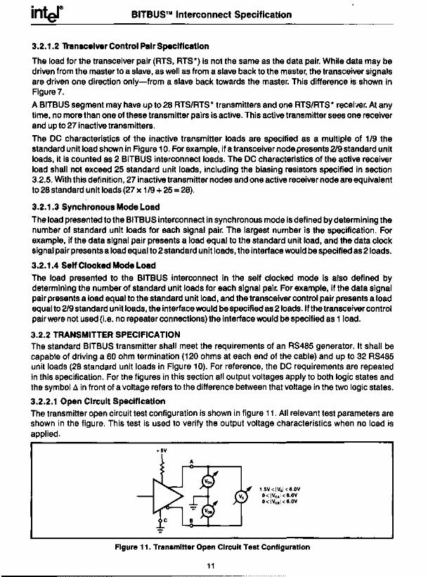
3.2.2.1 Open Circuit Specification The transmitter open circuit test configuration is shown in figure 11. All relevant test parameters are shown in the figure. This test is used to verify the output voltage characteristics when no load is applied.
+5V
A
1.5V<IVol<6.0V 0< IVo.1 <6.0V 0< IVo.1 <6.0V
Figure 11. TransmlHer Open Circuit Test Configuration
11
BITBUSTM Interconnect Specification
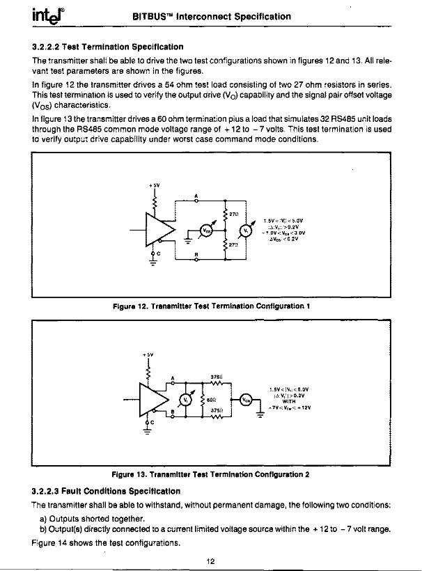
3.2.2.2 Test Termination Specification
The transmitter shall be able to drive the two test configurations shown in figures 12 and 13. All relevant test parameters are shown in the figures.
In figure 12 the transmitter drives a 54 ohm test load consisting of two 27 ohm resistors in series. This test termination is used to verify the output drive (Va) capability and the signal pair offset voltage (Vos) characteristics.
In figure 13 the transmitter drives a 60 ohm termination plus a load that simulates 32 RS485 unit loads through the RS485 common mode voltage range of + 12 to - 7 volts. This test termination is used to verify output drive capability under worst case command mode conditions.
+5V
A
1.5V< IV,I <5.0V laIV,II>0.2V
-1.0V<Vos<3.0V laVosl <0.2V
Figure 12. Transmitter Test Termination Configuration 1
+5V
3750
600
3750
1.5V< IV,I <5.0V laIV,II>0.2V
WITH -7V<VCM < +12V
Figure 13. Transmitter Test Termination Configuration 2
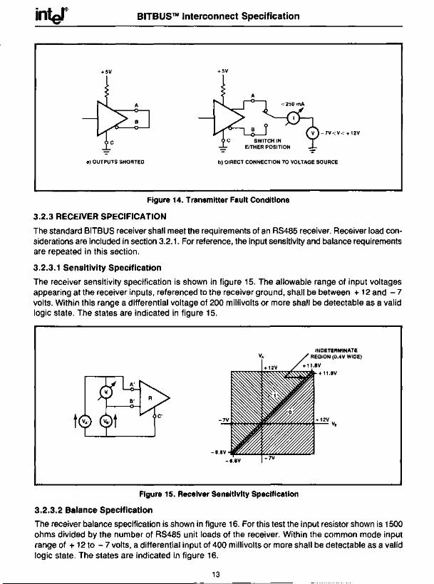
3.2.2.3 Fault Conditions Specification
The transmitter shall be able to withstand, without permanent damage, the following two conditions:
a) Outputs shorted together. b) Output(s) directly connected to a current limited voltage source within the + 12 to - 7 volt range.
Figure. 14 shows the test configurations.
12
BITBUSTM Interconnect Specification
+5V +5V
0) OUTPUTS SHORTEO b) OIRECT CONNECTION TO VOLTAGE SOURCE
Figure 14. Transmitter Fault Conditions
3.2.3 RECEIVER SPECIFICATION
The standard BITBUS receiver shall meet the requirements of an RS485 receiver. Receiver load considerations are included in section 3.2.1. For reference, the input sensitivity and balance requirements are repeated in this section.
3.2.3.1 Sensitivity Specification
The receiver sensitivity specification is shown in figure 15. The allowable range of input voltages appearing at the receiver inputs, referenced to the receiver ground, shall be between + 12 and - 7 volts. Within this range a differential voltage of 200 millivolts or more shall be detectable as a valid logic state. The states are indicated in figure 15.
Figure 15. Receiver Sensitivity Specification
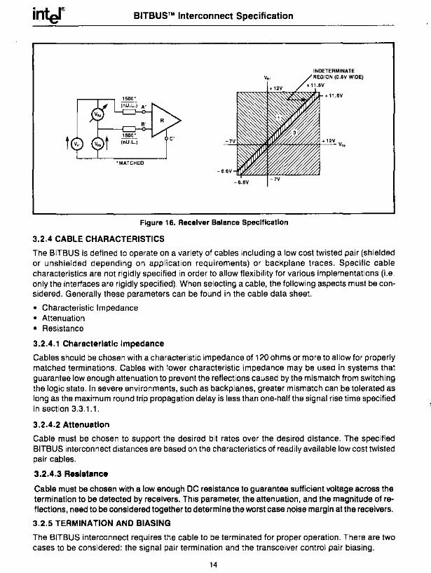
3.2.3.2 Balance Specification
The receiver balance specification is shown in figure 16. For this test the input resistor shown is 1500 ohms divided by the number of RS485 unit loads of the receiver. Within the common mode input range of + 12 to - 7 volts, a differential input of 400 millivolts or more shall be detectable as a valid logic state. The states are indicated in figure 16.
13
BITBUS™ Interconnect Specification
Figure 16. Receiver Balance Specification
3.2.4 CABLE CHARACTERISTICS
The BITBUS is defined to operate on a variety of cables including a low cost twisted pair (shielded or unshielded depending on application requirements) or backplane traces. Specific cable characteristics are not rigidly specified in order to allow flexibility for various implementations (Le. only the interfaces are rigidly specified). When selecting a cable, the following aspects must be considered. Generally these parameters can be found in the cable data sheet.
• Characteristic Impedance • Attenuation • Resistance
3.2.4.1 Characteristic Impedance
Cables should be chosen with a characteristic impedance of 120 ohms or more to allow for properly matched terminations. Cables with lower characteristic impedance may be used in systems that guarantee low enough attenuation to prevent the reflections caused by the mismatch from switching the logic state. In severe environments, such as backplanes, greater mismatch can be tolerated as long as the maximum round trip propagation delay is less than one-half the signal rise time specified in section 3.3.1.1.
3.2.4.2 Attenuation
Cable must be chosen to support the desired bit rates over the desired distance. The specified BITBUS interconnect distances are based on the characteristics of readily available low cost twisted pair cables.
3.2.4.3 Resistance
Cable must be chosen with a low enough DC resistance to guarantee sufficient voltage across the termination to be detected by receivers. This parameter, the attenuation, and the magnitude of reflections, need to be considered together to determine the worst case noise margin at the receivers.
3.2.5 TERMINATION AND BIASING
The BITBUS interconnect requires the cable to be terminated for proper operation. There are two cases to be considered: the signal pair termination and the transceiver control pair biasing.
14

BITBUSTM Interconnect Specification
3.2.5.1 Termination
All BITBUS interconnect cables must be terminated at both ends for proper operation. The terminations shall be located at the extreme ends of the cable. The value of each termination shall be 120 ohms or greater and should be chosen to match the characteristic impedance of the cable as closely as possible.
3.2.5.2 Transceiver Control Biasing
In addition to terminations, the transceiver control pair shall have biasing resistors at its receiver only node. These resistors shall be 470 ohms ± 5%, one being connected to + 5 volts ± 5% and the other connected to ground as shown in figure 7. The receiver only node may be located anywhere on the cable segment.
3.3 AC SPECIFICATIONS
The AC specifications for the BITBUS interconnect requires definition of the signal line characteristics, transmitter enable timing, self clocked mode timing. and repeater timing.
3.3.1 SIGNAL LINE CHARACTERISTICS
The BITBUS signal lines must maintain a reasonable level of signal integrity to guarantee proper operation. Specifically, there needs to be bounded rise and fall times and reflection guidelines.
3.3.1.1 Rise And Fall Time Specification
The BITBUS signal lines shall have rise and fall times between 25 and 1 OOns as shown in figure 17. This measurement shall be made in the test configuration shown in figure 18.
In actual systems, the rise and fall times may be slower than the above specification as long as the following two conditions are met.
a) The rise and fall time of any node shall meet the above specification (Figure 17) into the test load (Figure 18).
b) The rise and fall times in the actual system shall not be more than 0.3 times the bit cell width, measured anywhere in the system.
BIT CELL WIDTH
FOR MINIMUM PULSE
""" .-- - to.1 (J.V,)
J.V, / \ w_--/ --------- -----
\ -....... .- - to.1 (J.V,)
RISE FALL TIME TIME
Figure 17. Rise and Fall Specification
15
BITBUSTM Interconnect Specification
+5V
A
Figure 18. Test Configuration for Rise and Fall Time Measurement
3.3.1.2 Reflection Guidelines
Transitions on the BITBUS signal lines shall meet the requirements shown in figure 17 when driving the test load in figure 18. The transition from 10% to 90% of the final steady state value shall be monotonic. Ringing shall be limited to ± 10% around the final steady state value.
RS485 is a robust standard, providing a significant DC noise margin. In practical systems where reflections may be unavoidable these noise margins shall be used to guarantee proper operation. Potential reflections (due to lumped capacitive loads, mismatched terminations, or excessively long stubs) should be considered together with the DC losses specified in section 3.2.4 when choosing cable. In all cases, the voltage at any node shall remain in the + 12 volt to - 7 volt common mode range except for pulses of less than 15 microseconds, at less than 1 % duty cycle, which shall be bounded to ± 25 volts.
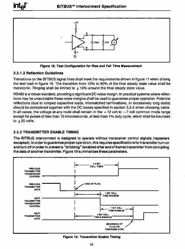
3.3.2 TRANSMITTER ENABLE TIMING
The BITBUS interconnect is designed to operate without transceiver control signals (repeaters excepted). In order to guarantee proper operation, this requires specifications for transmitter turn on and turn off in order to prevent a "dribbling" (enabled after end offrame) transmitter from corrupting the data of another transmitter. Figure 19 summarizes these parameters.
I 1-4 BIT I • CELL TIMES •
PREVIOUS _______ ---+ _________ ;1---------TRANSMITTER TRANSCEIVER
CONTROL
PREVIOUS -----, TRANSMITTER
DATA
:/ END OF FLAG
NEXT -------...;...------i TRANSMITTER I TRANSCEIVER
CONTROL I
TRANSMITTER •
1 BIT CELL TIME MINIMUM
NEXT I DATA -------...;...-------------i--........
BEGINNING OF FLAG OR
PREFRAME SYNC
Figure 19. Transmitter Enable Timing
16
BITBUSTM Interconnect Specification
Transmitters shall be enabled a least one bit cell time prior to valid data transmission (opening flag in synchronous mode, preframe synch in self clocked mode). A transmitter shall not be enabled until at least one bit cell time after detecting the closing flag of a previous frame. Finally a transmitter shall guarantee that the first valid bit of data is not transmitted until any previous transmitter has been disabled.
Transmitters shall be disabled between one and four bit cell times after the end of the closing flag. Note that this specification leads to a potential three bit cell time contention period during turn around. This is acceptable based on the fault condition specification of section 3.2.2.3.
3.3.3 SYNCHRONOUS MODE TIMING
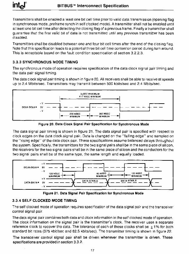
The synchronous mode of operation requires specification of the data clock signal pair timing and the data pair signal timing.
The data clock signal pair timing is shown in figure 20. All receivers shall be able to receive at speeds up to 2.4 Mbits/sec. Transmitters may transmit between 500 kbits/sec and 2.4 Mbits/sec.
21'SEC MAXIMUM I.. 411NSEC MINIMUM .. I DCLK·DCLK* ~~ -----.t - - - - --f - - - - - t - - - - f - -
1 200 NSEC .. I... 200 NSEC ~I
-MINIMUM - ..... --MINIMUM ~
Figure 20. Data Clock Signal Pair Specification for Synchronous Mode
The data signal pair timing is shown in figure 21. The data signal pair is specified with respect to clock edges on the data clock.signal pair. Data is changed on the "falling edge" and sampled on the "rising edge" of the data clock pair. These specifications assume balanced delays throughout the system. Specifically, the transmitters for the two signal pairs shall be in the same piece of silicon, the receivers for the two signal pairs shall be in the same piece of silicon and the conductors for the two signal pairs shall be of the same type, the same length and equally loaded.
DCLK·DCLK* ~~ - - -+ - - - f - - -1- - - -f - - - t- --120 NSEC I I 80 NSEC I I 120 NSEC-I MAXIMUM .... MINIMUM.... .. MINIMUM
DATA.DATA* ~~ ____ *_~A~A~_~--~A~~--E
Figure 21. Data Signal Pair Specification for Synchronous Mode
3.3.4 SELF CLOCKED IIiIODE TIMING
The self clocked mode of operation requires specification of the data signal pair and the transceiver control signal pair.
The data signal pair combines both data and clock information in the self clocked mode of operation. The clock information on the signal pair is the transmitter's clock. The receiver uses a separate reference clock to recover the data. The tolerance of each of these clocks shall be ± 1 % for both standard bit rates (375 kbitlsec and 62.5 kbits/sec). The transmitter timing is shown in figure 22.
The transceiver control signal pair shall be driven whenever the transmitter is driven. These specifications are provided in section 3.3.2.
17
int:er BITBUSTM Interconnect Specification
I_ ICELL "I DATA-DATA* ~: ---... t - - - - =1 ..... -----------------------+ - -
tCELL
375 Kb/SEC
2.640 !,SEC MIN 2.693 !,SEC MAX
62.5 Kb/SEC
15.84 ~SEC MIN 16.16 ~SEC MAX
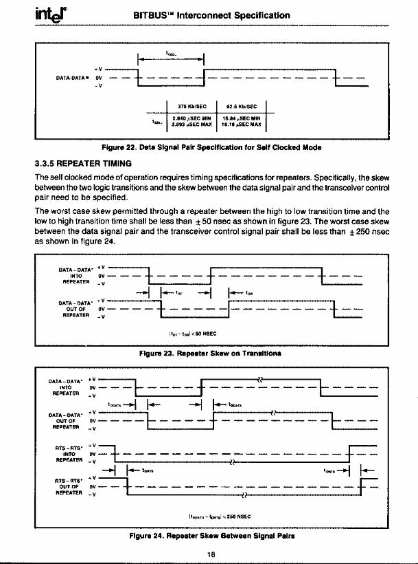
Figure 22. Data Signal Pair Specification for Self Clocked Mode
3.3.5 REPEATER TIMING
The self clocked mode of operation requires timing specifications for repeaters. Specifically, the skew between the two logic transitions and the skew between the data signal pair and the transceiver control pair need to be specified.
The worst case skew permitted through a repeater between the high to low transition time and the low to high transition time shall be less than ± 50 nsec as shown in figure 23. The worst case skew between the data signal pair and the transceiver control signal pair shall be less than ± 250 nsec as shown in figure 24.
D::1~~r::' ~: - - - + ----+ --------+ ---__ -1.....:........;1-10, -I ;-1-_10_0 ___ ---.
D:~::;~:' ~:- --_ + __ -- _1_ - -- - - - - + --
DATA-DATA' INTO
REPEATER
DATA-DATA' OUT OF
REPEATER
RTS-RTS' INTO
REPEATER
RTS-RTS' OUT OF
REPEATER
110, -IDol < 50 NSEC
Figure 23. Repeater Skew on Transitions
+V 22
:---~----t---------~----IDDATA -l I- -l I- I .. ATA
+V lZ
:----~----t---------~---
:~=t - - - -- - - - - -- - -- - -- - f---v u
--l 1- 10." IDRTS -I I-:~- -+------------------F -v u
II00ATA -IDRTSI < 250 NSEC
Figure 24. Repeater Skew Between Signal Pairs
18
inter BITBUSTM Interconnect Specification
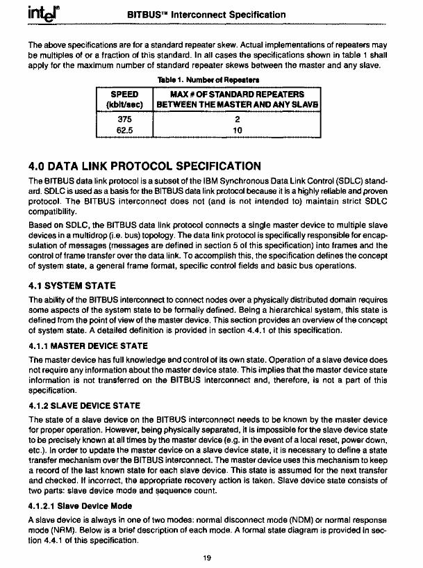
The above specifications are for a standard repeater skew. Actual implementations of repeaters may be multiples of or a fraction of this standard. In all cases the specifications shown in table 1 shall apply for the maximum number of standard repeater skews between the master and any slave.
"nIble 1. Number of Repeaters
SPEED MAX # OF STANDARD REPEATERS (kbltlsec) BETWEEN THE MASTER AND ANY SLAVS
375 2 62.5 10
4.0 DATA LINK PROTOCOL SPECIFICATION The BITBUS data link protocol is a subset of the IBM Synchronous Oata Link Control (SOLC) standard. SOLC is used as a basis for the BITBUS data link protocol because it is a highly reliable and proven protocol. The BITBUS interconnect does not (and is not intended to) maintain strict SOLC compatibility.
Based on SOLC, the BITBUS data link protocol connects a single master device to multiple slave devices in a multidrop (i.e. bus) topology. The data link protocol is specifically responsible for encapsulation of messages (messages are defined in section 5 of this specification) into frames and the control of frame transfer over the data link. To accomplish this, the specification defines the concept of system state, a general frame format, specific control fields and basic bus operations.
4.1 SYSTEM STATE
The ability of the BITBUS interconnect to connect nodes over a physically distributed domain requires some aspects of the system state to be formally defined. Being a hierarchical system, this state is defined from the point of view of the master device. This section provides an overview of the concept of system state. A detailed definition is provided in section 4.4.1 of this specification.
4.1.1 MASTER DEVICE STATE
The master device has full knowledge and control of its own state. Operation of a slave device does not require any information about the master device state. This implies that the master device state information is not transferred on the BITBUS interconnect and, therefore, is not a part of this specification.
4.1.2 SLAVE DEVICE STATE
The state of a slave device on the BITBUS interconnect needs to be known by the master device for proper operation. However, being physically separated, it is impossible for the slave device state to be precisely known at all times by the master device (e.g. in the event of a local reset, power down, etc.). In order to update the master device on a slave device state, it is necessary to define a state transfer mechanism over the BITBUS interconnect. The master device uses this mechanism to keep a record of the last known state for each slave device. This state is assumed for the next transfer and checked. If incorrect, the appropriate recovery action is taken. Slave device state consists of two parts: slave device mode and ~equence count.
4.1.2.1 Slave Device Mode
A slave device is always in one of two modes: normal disconnect mode (NOM) or normal response mode (NRM). Below is a brief description of each mode. A formal state diagram is provided in section 4.4.1 of this speCification.
19
inter BITBUSTM Interconnect Specification
A slave device enters NDM after'a local reset or when it detects an irrecoverable protocol error. In this mode, a slave is awaiting a specific command from the master device to enter NRM. A slave device may not exchange messages with the master device in this mode. A slave device enters NRM only after receiving a specific command from the master device. Upon entering NRM, a slave device is "synchronized" with the master device, meaning that all sequence counts match (they are all initialized to 0). In this mode, a slave device may exchange messages with the master device as long as "synchronization" is maintained (i.e. no sequence count errors).
4.1.2.2 Sequence Counts In NRM, sequence counts are used by the master device and each slave device to guarantee that frames are not lost or duplicated. Below is a brief description of how sequencing works. Further details are provided in section 4.3 of this specification. Sequencing is performed by the master device and each slave device via two pairs of 3 bit sequence counts. Each slave keeps an N, (number received) sequence count and an Ns (number sent) sequence count. The master device keeps a corresponding pair of counts for each slave it communicates with. A slave device is "synchronized" with the master device when the sequence counts are correct. The sequence counts at a slave device are considered part of the slave device state. The sequence counts at the master device are the master device's best knowledge of the slave device state. The N, sequence count indicates the sequence count of the next expected incoming message. The Ns sequence count indicates the sequence count of the next message awaiting acknowledgement (mayor may not be outstanding). Each time a transfer occurs in NRM these numbers are included and verified resulting in three possible outcomes: correct sequence count, recoverable sequence error or irrecoverable sequence error. The irrecoverable sequence count error case requires the master device to resynchronize with the slave device by causing it to return to NDM, then re-enter NRM. The other cases allow the slave device to remain in NRM. Further details are provided later in this specification.
4.2 FRAME FORMAT The data link protocol is responsible for creating frames to be transferred across the BITBUS interconnect. All frames use the frame format shown in figure 25. All fields are composed of one or more bytes (plus possible zero bit insertion), with the least significant bit (LSB) of each byte transmitted first. The only exception is the frame check sequence field, which transmits the most significant bit of each byte first.
4.2.1 FLAG FIELDS
I FLAG I ADDRESS I CONTROL I INFORMATION I FCS I FLAG I { NUMBER
N 2 1 OF BYTES
Figure 25. Standard Frame Format
The flag fields are used to delimit the frame. These fields (one at the beginning of the frame and one at the end of the frame) contain the unique bit pattern 01111110. The uniqueness of this bit pattern is guaranteed by using zero bit insertion/deletion in all other fields as described in section 3 of this specification. These fields are required in all frames.
4.2.2 ADDRESS FIELD
The address field contains the address of the slave device involved in the transfer. For a transmitting master device, this field identifies the destination slave device. For a transmitting slave device, this
20
BITBUSTM Interconnect Specification
field identifies the source slave device to the master device. If this field does not match the slave device address, the frame is ignored. The address field is eight bits long and may contain values from o to 255. Values 0 and 251-255 are reserved by Intel. All others may be used without restriction. This field is required in all frames.
4.2.3 CONTROL FIELD
The control field is used for command and status exchange between the master device and slave devices. This field is eight bits long and is used for three classes of operations: synchronization, supervision and message transfer. Below is an overview of these operations. Details are provided in section 4.3 of this specification. This field is required in all frames.
4.2.3.1 Synchronization
The transfer of sequenced messages between the master device and a slave device requires that the slave device be properly synchronized to the master device. This synchronization process is performed using unnumbered frames (i.e. frames with unnumbered control fields). As the name implies, unnumbered frames do not use the sequencing feature.
4.2.3.2 Supervision
After the master device is synchronized with a slave device, it is often necessary to exchange status information in the absence of messages. This is done with supervisory frames (i.e. frames with supervisory control fields). These frames are used by the master device to poll a slave device and by a slave device to acknowledge receipt of a valid frame (i.e. address match and no CRC error) from the master device.
4.2.3.3 Information
Information frames (i.e. with information control fields) are used by the master device or a slave device to transfer messages (messages are defined in section 5 of this specification). These frames are only used after synchronization, as are supervisory frames. In addition to a message and its sequence count, information frames carry the same status information as supervisory frames. In fact, information frames may be considered a superset of supervisory frames.
4.2.4 INFORMATION FIELD
The information field is used to carry the BITBUS message. Details of this field are provided in section 5 of this specification. This field is required for information frames and is not used for supervisory or unnumbered frames.
4.2.5 FRAME CHECK SEQUENCE FIELD
The frame check sequence (FCS) field provides the lowest level of error detection on the BITBUS interconnect. This field contains a 16 bit cyclic redundancy check (CRC). The transmitting node generates and sends this field, while the receiving node checks it for correctness. A receiving node ignores an incoming frame if the CRC is incorrect. The CRC is generated by the standard CRCCCITT polynomial X 16 + X12 + X5 + 1. This field is required in all frames. Unlike other fields, the most significant bit of each byte is transmitted first, and the most significant byte is also transmitted first.
4.3 CONTROL FIELD DEFINITION
Operations on the BITBUS interconnect are performed using three types of control fields: unnumbered, supervisory and information. This section specifies these fields in detail and explains their usage.
For reference to SDLC, this specification uses a subset of the defined control fields with the poll/final bit always set. This implies that frames sent by the master device always expect a response from
21
inter BITBUSTM Interconnect Specification
the addressed slave device (poll bit set) and that frames sent by slave devices always return control of the link (final bit set) to the master device.
4.3.1 UNNUMBERED FRAMES
Unnumbered frames are used on the BITBUS interconnect for synchronizing slave devices with the master device. This section specifies the control field format for these frames and defines the unnumbered operations (commands and responses) supported on the BITBUS interconnect.
4.3.1.1 Unnumbered Control Field Format
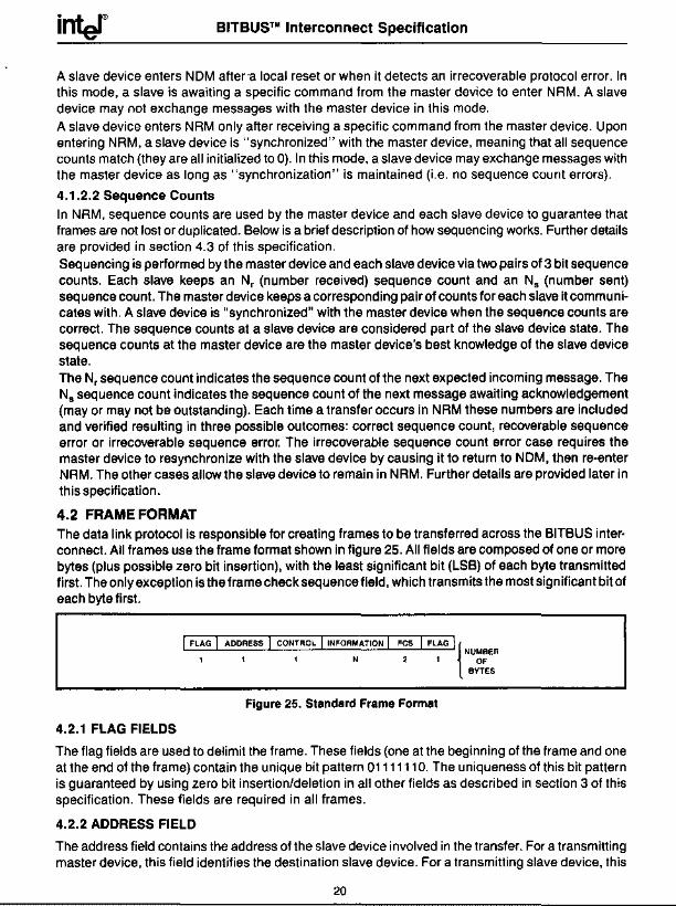
The control field format for unnumbered frames is shown in figure 26. This field may specify one of several unnumbered operations.
\ • ''''-v---J
.... 1 ___ -L.I ___ OPERATION SPECIFIC CODE
Figure 26. Unnumbered Control Field Format
4.2.1.2 Unnumbered Operations
The BITBUS interconnect supports two unnumbered commands (SNRM and DISC) and two unnumbered responses (UA and FRMR). The control fields for these operations are summarized in table 2.
Table 2. Unnumbered Control Fields
OPERATION COMMAND RESPONSE CONTROL VALUE FIELD
SNRM ", 93H DISC ", 53H UA ", 73H
FRMR ", 97H
/' The frame reject (FRMR) command is sent to the master device by a slave device that detects an invalid control field in an otherwise valid frame. It is also used by a slave to respond to any unnumbered frame while in NRM, any supervisory or information frame while in NDM, any unsupported control field, or an irrecoverable sequence count error. Upon receiving this command, the master device initiates resynchronization with the slave device.
The unnumbered acknowledge (UA) response is used by a slave device to acknowledge receipt of a valid unnumbered command while in NDM.
The disconnect (DISC) command is sent by the master device to a slave device to initiate resynchronization. This command causes the slave device to go to, or stay in, NDM. It is used by the master device when it detects the need to resynchronize (e.g. after reset, irrecoverable sequence error, etc. or in response to an FRMR from a slave device. When the master device receives a UA in response to a DISC it knows that the addressed slave device is in NDM.
The set normal response mode (SNRM) command is sent by the master device to synchronize a slave device. If a slave device is in NDM, this command causes it to enter NRM, allowing it to exchange messages with the master device. If a slave device is already in NRM, this command is invalid, causil)~ the slave to reply with FRMR and enter NDM.
22
inter BITBUSTM Interconnect Specification
4.3.2 SUPERVISORY FRAMES
Supervisory frames are used on the BITBUS interconnect for passing status between the master device and a slave device while in NRM. These frames are used by a master device to poll slave devices and by slave devices to acknowledge receipt of a valid frame from the master device. This section specifies the control field format for these frames and defines the specific control fields that are supported.
4.3.2.1 Supervisory Control Field Format
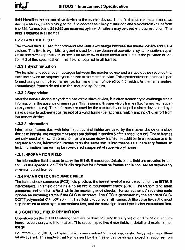
The control field format for supervisory frames is shown in Figure 27. This field is used'to specify the supervisory operation (RR or RNR) as well as to acknowledge receipt of a previous message via the Nr sequence count.
LSB (FIRST TRANSMITTED) rl-r-'-'I-l'l~o'I--lro-rl~l I
, '-.,.-I
L-{O-RR l-RNR L..-_______ . N, SEQUENCE COUNT
Figure 27. Supervisory Control Field Format
4.3.2.2 Supervisory Operation
The BITBUS interconnect supports two supervisory operations: receiver ready (RR) and receiver not ready (RNR).
The master device uses the RR supervisory frame to poll a slave device for an information frame. Slave devices use the RR supervisory frame to acknowledge valid reception (i.e. address match, valid CRC and available buffer space) of a previous supervisory or information frame when a message is not available (If a message is available an information frame is sent unless the incoming frame was a RNR supervisory frame).
The RNR supervisory frame is used to indicate that a buffer is presently unavailable to receive an otherwise valid frame. The master device uses the RNR supervisory frame to poll a slave device for data link status only. A slave device shall not respond to a RNR supervisory frame with an information frame. A slave device uses the RNR supervisory frame to indicate that the last frame was recognized, however there was no buffer available to store it. In this case the master device shall retransmit the frame.
Both RR and RNR frames contain an Nr sequence count. This sequence count acknowledges receipt of Nr-1 frames (i.e. Nr equals the next expected incoming frame). The receiver of a supervisory frame shall always compare this value to its Ns sequence count for correctness.
In the case that all messages have been acknowledged, the incoming Nr sequence count should equal the Ns sequence count. If the previous frame sent by the receiving node was an information frame, then the incoming Nr sequence count should equal the Ns sequence count plus 1. If this case is true, the previous frame is acknowledged meaning the Ns sequence can be incremented and the message buffer released. If after an information frame the incoming Nr sequence count is equal to the Ns sequence count, the information frame was not received and shall be retransmitted. Any other Nr sequence count value is detected as an irrecoverable sequence error requiring the master device to resynchronize with the slave device.
23
BITBUSTM Interconnect Specification
4.3.3 INFORMATION FRAMES
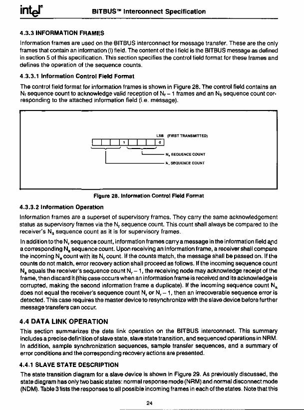
Information frames are used on the BITBUS interconnect for message transfer. These are the only frames that contain an information (I) field. The content of the I field is the BITBUS message as defined in section 5 of this specification. This section specifies the control field format for these frames and defines the operation of the sequence counts.
4.3.3.1 Information Control Field Format
The control field format for information frames is shown in Figure 28. The control field contains an Nr sequence count to acknowledge valid reception of Nr - 1 frames and an Ns sequence count corresponding to the attached information field (Le. message).
'---"T""""""""T""""""T""--'---'_r-TL_S.,B (FIRST TRANSMITTED)
I I 1 I I 0 I , .J \, .J
L..-__ N. SEQUENCE COUNT
'---------N, SEQUENCE COUNT
Figure 28. Information Control Field Format
4.3.3.2 Information Operation
Information frames are a superset of supervisory frames. They carry the same acknowledgement status as supervisory frames via the Nr sequence count. This count shall always be compared to the receiver's Ns sequence count as it is for supervisory frames.
In addition to the Nr sequence count, information frames carry a message in the information field a.,.nd a corresponding Ns sequence count. Upon receiving an information frame, a receiver shall compare the incoming Ns count with its Nr count. If the counts match, the message shall be passed on. If the counts do not match, error recovery action shall proceed as follows. If the incoming sequence count Ns equals the receiver's sequence count Nr - 1 , the receiving node may acknowledge receipt of the frame, then discard it (this case occurs when an information frame is received and its acknowledge is corrupted, making the second information frame a duplicate). If the incoming sequence count Ns does not equal the receiver's sequence count Nr or Nr - 1 , then an irrecoverable sequence error is detected. This case requires the master device to resynchronize with the slave device before further message transfers can occur.
4.4 DATA LINK OPERATION This section summarizes the data link operation on the BITBUS interconnect. This summary includes a precise definition of slave state, slave state transition, and sequenced operations in NRM. In addition, sample synchronization sequences, sample transfer sequences, and a summary of error conditions and the corresponding recovery actions are presented.
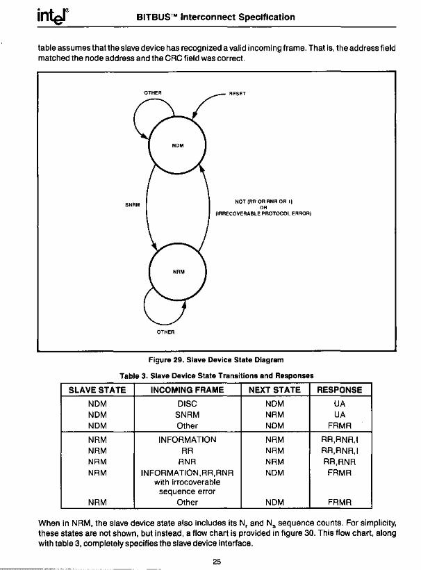
4.4.1 SLAVE STATE DESCRIPTION
The state transition diagram for a slave device is shown in Figure 29. As previously discussed, the state diagram has only two basic states: normal response mode (NRM) and normal disconnect mode (NOM). Table 3 lists the responses to all possible incoming frames in each of the states. Note that this
24
inter BITBUSTM Interconnect Specification
table assumes that the slave device has recognized a valid incoming frame. That is, the address field matched the node address and the CRC field was correct.
OTHER
RESET
NOT (RR OR RNR OR i) OR
(iRRECOVERABLE PROTOCOL ERROR)
Figure 29. Slave Device State Diagram
Table 3. Slave Device State Transitions and Responses
SLAVE STATE INCOMING FRAME NEXT STATE
NDM DISC NDM NDM SNRM NRM NDM Other NDM
NRM INFORMATION NRM NRM RR NRM NRM RNR NRM NRM INFORMATION,RR,RNR NDM
with irrocoverable sequence error
NRM Other NDM
RESPONSE
UA UA
FRMR
RR,RNR,I RR,RNR,I RR,RNR FRMR
FRMR
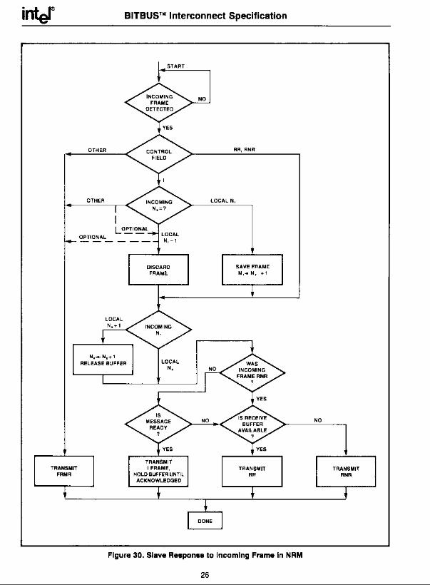
When in NRM, the slave device state also includes its Nr and Ns sequence counts. For simplicity, these states are not shown, but instead, a flow chart is provided in figure 30. This flow chart, along with table 3, completely specifies the slave device interface.
25
inter
TRANSMIT FRMR
BITBUS™ Interconnect Specification
OTHER
OTHER
OPTIONAL
N ..... N.+1 RELEASE BUFFER
N,-1
DISCARD FRAM~
TRANSMIT I FRAME,
HOLD BUFFER UNTIL ACKNOWLEDGED
RR,RNR
SAVE FRAME Nr .... N, +1
TRANSMIT RR
Figure 30. Slave Response to Incoming Frame In NRM
26
NO
TRANSMIT RNR
inter BITBUSTM Interconnect Specification
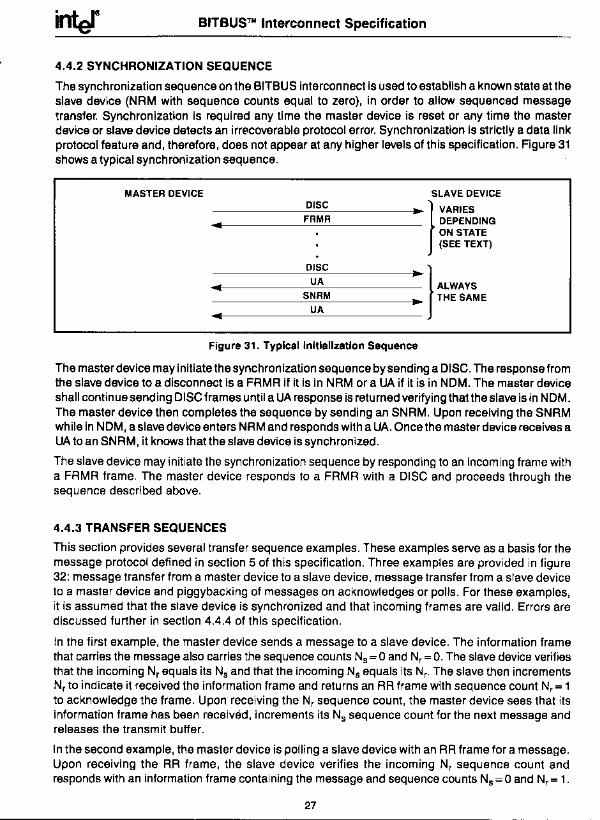
4.4.2 SYNCHRONIZATION SEQUENCE
The synchronization sequence on the BITBUS interconnect is used to establish a known state at the slave device (NRM with sequence counts equal to zero), in order to allow sequenced message transfer. Synchronization is required any time the master device is reset or any time the master device or slave device detects an irrecoverable protocol error. Synchronization is strictly a data link protocol feature and, therefore, does not appear at any higher levels of this specification. Figure 31 shows a typical synchronization sequence.
MASTER DEVICE SLAVE DEVICE DISC ~ } VARIES
• FRMR DEPENDING ON STATE (SEE TEXT)
DISC
~} • UA ALWAYS SNRM • THE SAME .. UA
Figure 31. Typical Initialization Sequence
The master device may initiate the synchronization sequence by sending a DISC. The response from the slave device to a disconnect is a FRMR if it is in NRM or a UA if it is in NOM. The master device shall continue sending DISC frames until a UA response is returned verifying thatthe slave is in NOM. The master device then completes the sequence by sending an SNRM. Upon receiving the SNRM while in NOM, a slave device enters NRM and responds with a UA. Once the master device receives a UA to an SNRM, it knows that the slave device is synchronized.
The slave device may initiate the synchronization sequence by responding to an incoming frame with a FRMR frame. The master device responds to a FRMR with a DISC and proceeds through the sequence described above.
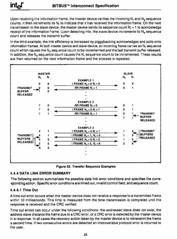
4.4.3 TRANSFER SEQUENCES
This section provides several transfer sequence examples. These examples serve as a basis for the message protocol defined in section 5 of this specification. Three examples are provided in figure 32: message transfer from a master device to a slave device, message transfer from a slave device to a master device and piggybacking of messages on acknowledges or polls. For these examples, it is assumed that the slave device is synchronized and that incoming frames are valid. Errors are discussed further in section 4.4.4 of this specification.
In the first example, the master device sends a message to a slave device. The information frame that carries the message also carries the sequence counts Ns = 0 and Nr = O. The slave device verifies t~at the incoming Nr equals its Ns and that the incoming Ns equals its Nr. The slave then increments Nr to indicate it received the information frame and returns an RR frame with sequence count Nr = 1 to acknowledge the frame. Upon receiving the Nr sequence count, the master device sees that its information frame has been received, increments its Ns sequence count for the next message and releases the transmit buffer.
In the second example, the master device is polling a slave device with an RR frame for a message. Upon receiving the RR frame, the slave device verifies the incoming Nr sequence count and responds with an information frame containing the message and sequence counts Ns = 0 and Nr = 1.
27
BITBUSTM Interconnect Specification
Upon receiving the information frame, the master device verifies the incoming Nr and Ns sequence counts. It then increments its Nr to indicate that it has received the information frame. On the next transmission to the slave device, the master device sends its sequence count Nr = 1 to acknowledge receipt of the information frame. Upon detecting this, the slave device increments its Ns sequence count and releases the transmit buffer.
In the third example, the link efficiency is increased by piggybacking acknowledges and polls onto information frames. At both master device and slave device, an incoming frame carries an Nr sequence count which causes the Ns sequence count to be incremented and the last transmit buffer released. In addition, the Ns sequence count causes the Nr sequence count to be incremented. These results are then returned on the next information frame and the process is repeated.
MASTER N.
0
TRANSMIT ~ BUFFER 1 RELEASED
4
TRANSMIT}C4 BUFFERS 5 RELEASED 5
6
N,
0
0 0
0
0
1
2 2
3
...
...
..
..
EXAMPLE 1 I FRAME N.=O N,=O
RR FRAME N, = 1
EXAMPLE 2 RR FRAME N,=O
I FRAME N.=O N,= 1 RR FRAME N, = 1
EXAMPLE 3 I FRAME N.=4 N,= 1 I FRAME N.= 1, N,=5
I·FRAME N.=5 N,=2 I FRAME N.=2, N,=6
~
~
~
~
Figure 32. Transfer Sequence Examples
4.4.4 DATA LINK ERROR SUMMARY
SLAVE N. N,
o o
0
0
0
2
o
1
1 TRANSMIT 1"-BUFFER
RELEASED
brANSMIT 5 BUFFERS 5 RELEASED
6
The following section summarizes the possible data link error conditions and specifies the corresponding action. Specific error conditions are timed out, invalid control field, and sequence count.
4.4.4.1 Time Out
A time out error occurs when the master device does not receive a response to a transmitted frame within 10 milliseconds. This time is measured from the time transmission is completed until the response is received and the CRC verified.
Time out errors can occur under the following conditions: the addressed slave does not exist, the address slave discards the frame due to a CRC error, or a CRC error is detected by the master device in a response. In all cases the recovery action taken by the master device is to retransmit the frame a second time. If two consecutive errors are detected an irrecoverable protocol error is returned to the user.
28
BITBUSTM Interconnect Specification
4.4.4.2 Invalid Control Field
An invalid control field detected by either the master device or a slave device is considered an irrecoverable protocol error. Detection of this error condition at a slave device causes the slave device to enter NOM and respond with a FRMR. Detection at the master device causes it to assume that the slave is in NOM, requiring resynchronization.
4.4.4.3 Sequence Count
Sequence count errors are recoverable in some cases as indicated in figure 30. Cases that are not recoverable are considered irrecoverable protocol errors. Detection of an irrecoverable condition at a slave device causes it to enter NOM and respond with a FRMR. Detection at the master device causes it to assume that the slave is in NOM, requiring resynchronization.
5.0 MESSAGE PROTOCOL SPECIFICATION The BITBUS message protocol is designed to provide a task to task message interface between a master node and multiple slave nodes using an order/reply structure. That is, the master node issues orders to slave nodes which respond with replies. This structure is built on top of the data link protocol using information frames for the message transfer. This section specifies the order/reply structure (including error handling) and the standard message format.
5.1 ORDER/REPL Y STRUCTURE
The BITBUS message protocol is based on an order/reply structure in a multitasking environment. An order is defined as a message that is sent by a task on the master node, over the BITBUS interconnect, to a task on a slave node. A reply is defined as a message that is sent by a task on a slave node, over the BITBUS interconnect, to a task on the master node, in response to an order from that master node task. Master node tasks may exist on either the master device or master device extension (collectively referred to as the master node). Likewise, slave node tasks may exist on either the slave device or slave device extension (collectively referred to as the slave node). Note that orders and replies may have a more general definition when used between tasks on a given node. This special case is not part of this specification.
Every order on the BITBUS interconnect requires a corresponding reply; however, replies need not be returned in the same sequence that orders are issued. For example, if the master print node issues orders A,B,C to a slave node, the responses may be returned as A,B,C or B,C,A or C,A,B, etc. Based on this requirement, a master device need only poll a slave node when one or more orders are outstanding. This condition exists when the sequence counts N, and Ns for a given slave node are not equal. When the sequence counts N, and Ns are equal, the slave node has no more replies and need not be polled. This algorithm limits unnecessary polling and increases system performance.
The data link protocol provides sequence counts that are 3 bits long. This limits the number of outstanding messages to any given slave node to seven. The slave node is responsible for enforcing this limit by not providing a receive buffer for the eighth message.
The BITBUS message protocol provides sufficient control to route orders from the master node to a slave device or slave device extension, and route replies from a slave node to a master device or master device extension. This capability allows local messages within a node to co-exist in a common gateway implementation. Furthermore, multiple level hierarchies (as shown in figure 1) are easily supported using the same master device software. The details of these implementations are not part of this specification.
Several sources of error exist in the message protocol. Specific examples are irrecoverable protocol errors or missing tasks. In all cases, the BITBUS message protocol detects the errors and handles
29
inter BITBUSTM Interconnect Specification
them in the same way. If an error occurs while delivering an order, the complete order is immediately converted to a reply and returned to the originating task. The reply is identical to the order except for the error code in the response field. If an error is detected on a reply, it is simply discarded (note that this is a very rare case, except for catastrophic error, since the reply retraces the path of the order). In either case, there is a small possibility that a reply is not returned. The task originating the order must account for this by setting a time out period for recovery. Note that this time out is not related to the data link time out specified in section 4 of this specification. Its value is determined by the application.
5.2 MESSAGE FORMAT
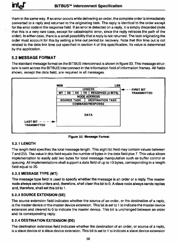
The standard message format on the BITBUS interconnect is shown in figure 33. This message structure is sent across the BITBUS interconnect in the information field of information frames. All fields shown, except the data field, are required in all messages.
LAST BIT - - - ..... TRANSMITTED
5.2.1 LENGTH
MSB LSB LENGTH
MT I SE I DE I TR I RESERVED (4 BITS1 NODE ADDRESS
SOURCE TASK I DESTINATION TASK COMMAND/RESPONSE
DATA
Figure 33. Message Format
~ - - FIRST BIT TRANSMITTED
The length field specifies the total message length. This eight bit field may contain values between 7 and 255. The value in this field equals the number of bytes in the data field plus 7. This value allows implementation to easily add two bytes for local message manipulation such as buffer control or queuing. All implementations shall support a data field of up to 13 bytes, corresponding to a length field equal to 20.
5.2.2 MESSAGE TYPE (MT)
The message type field is used to specify whether the message is an order or a reply. The master node always sends orders and, therefore, shall clear this bit to O. A slave node always sends replies and, therefore, shall set this bit to 1.
5.2.3 SOURCE EXTENSION (SE)
The source extension field indicates whether the source of an order, or the destination of a reply, is the master device or the master device extension. This bit is set to 1 to indicate the master device extension and cleared to 0 to indicate the master device. This bit is unchanged between an order and its corresponding reply.
5.2.4 DESTINATION EXTENSION (DE)
The destination extension field indicates whether the destination of an order, or source of a reply, is a slave device or a slave device extension. This bit is set to 1 to indicate a slave device extension
30
inter BITBUSTM Interconnect Specification
and cleared to 0 to indicate a slave device. This bit is unchanged between an order and its corresponding reply.
5.2.5 TRACK (TR)
The track field is used to provide message control at a master or slave device which may be required by some implementations. This bit is cleared to 0 when sending a message. It is set to 1 upon receiving a message from the BITBUS interconnect.
5.2.6 RESERVED
These four bits are reserved for possible future enhancements. They shall be cleared to zero when sending a message and their value is not guaranteed upon receiving a message.
5.2.7 NODE ADDRESS
The node address field specifies the destination node for orders and the source node for replies (Le. it is unchanged between order and reply). This eight bit field contains the same value as the address field in the data link frame. Valid entries are 1 through 250. The values 0 and 251-255 are reserved by Intel.
5.2.8 SOURCE TASK
The source task field identifies the task that has generated an order or is to receive a reply. This four bit field allows up to sixteen tasks to generate orders from the master device and the master device extension. Specific implementations may support as few as one or as many as sixteen tasks.
5.2.9 DESTINATION TASK
The destination task field identifies the task that is to receive an order or has generated a reply. This four bit field allows up to sixteen tasks to receive orders at each slave device and slave device extension. Specific implementations may support as few as one or as many as sixteen tasks.
5.2.10 COMMAND/RESPONSE
The command/response field is used by both user tasks and the message protocol. Under normal conditions, this field is used only by the user tasks. The message protocol only uses this field for reporting errors. Table 4 indicates the usage of this field. Note that this table only applies to responses. Commands are always defined by the user task.
Table 4. Message Protocol Responses
CONDITION ERROR
No error (set by user) OOH
User defined 01H-7FH
No destination task 80H
Protocol Error 91H No destination device 93H Reserved by Intel 81 H-90H,92H,
94H-OFFH
5.2.11 DATA
The data field is defined by the contents of the command field. Minimum support requires this field to be capable of handling 13 bytes. Implementation may extend it to as much as 248 bytes provided that the longer messages are not sent to nodes that cannot support them. This field is the only optional field in the message.
31
inter BITBUSTM Interconnect Specification
6.0 REMOTE ACCESS AND CONTROL SPECIFICATION The remote access and control (RAG) interface for the BITBUS interconnect defines a set of high level commands and responses to perform general purpose operations at a slave node. The remote access interface allows I/O read and write capabilities as well as memory download and upload. The remote control interface allows control and monitoring of tasks at a slave node. The RAC interface is built on top of the message protocol defined in section 5 of this specification. In fact, RAC is simply a special task defined at slave nodes. This section specifies the commands, responses and the general RAC message format.
6.1 MESSAGE FORMAT FOR RAC
The RAC interface is built on top of the standard message protocol. The message format follows the standard format in figure 33 with the following fields further defined: destination task, command/ response, and data.
6.1.1 DESTINATION TASK
The BITBUS interconnect, by convention, defines task 0 as the RAC task. This makes its presence easily detectable and allows it to be addressed in the same way for all implementations. If the RAC task is not supported at a slave node, task 0 may be used for another function.
6.1.2 COMMAND/RESPONSE
The command/response field is used to identify the RAC command in an order message and the RAC response in reply messages. The various commands and responses supported by the RAC interface are specified in sections 6.2 and 6.3, respectively.
6.1.3 DATA
The contents of the data field are determined by the RAC.command. The length field is used to identify the exact number of data bytes. The minimum BITBUS interconnect support provides up to 13 bytes in this field. Details of this field are provided in sections 6.2 and 6.3 of this specification.
6.2 RAC COMMANDS
Table 5 lists the RAC commands supported on the BITBUS interconnect. Commands OOH through OBFH are general purpose commands controlled by Intel. At this time, 15 are specifically defined, and the rest are reserved. Commands OCOH through OFFH are available to the user for custom RAC commands. These values will not be standardized. Specific implementations of RAC may support all or any subset of the defined commands. The only specific requirements are that the implementation return an error response for unsupported commands and that all supported general purpose commands conform to this specification.
6.2.1 CREATE TASK
The create task command is used to initialize and begin execution of a task at a slave node. This command assumes that the task to be created is already in the slave node memory. The command is simply the mechanism used to inform the operating system at the slave node that a given task in memory is to become active.
The data field in a create task order contains an address pointer (length field equal to 7 plus pointer length) to the task descriptor in the slave node's memory. The length of the pointer is determined by the implementation requirements at the slave node. This pointer is sent most significant byte first. The actual task descriptor may vary between implementations and, therefore, is not part of this specification.
32
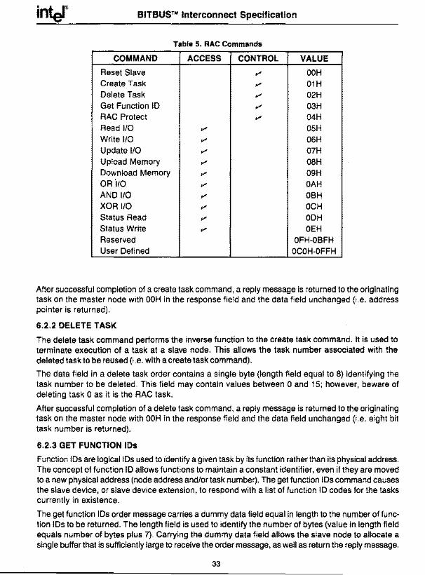
BITBUSTM Interconnect Specification
Table 5. RAC Commands
COMMAND ACCESS CONTROL VALUE
Reset Slave ",. OOH Create Task ",. 01H Delete Task ",. 02H Get Function 10 ",. 03H RAC Protect ",. 04H Read I/O ",. 05H Write I/O ",. 06H Update I/O ",. 07H Upload Memory ",. 08H Download Memory ",. 09H OR ·1/0 ",. OAH AND I/O ",. OSH XOR I/O ",. OCH Status Read ",. ODH Status Write ",. OEH Reserved OFH-OSFH User Defined OCOH-OFFH
After successful completion of a create task command, a reply message is returned to the originating task on the master node with OOH in the response field and the data field unchanged (i.e. address pointer is returned).
6.2.2 DELETE TASK
The delete task command performs the inverse function to the create task command. It is used to terminate execution of a task at a slave node. This allows the task number associated with the deleted task to be reused (i.e. with a create task command).
The data field in a delete task order contains a single byte (length field equal to 8) identifying the task number to be deleted. This field may contain values between 0 and 15; however, beware of deleting task 0 as it is the RAC task.
After successful completion of a delete task command, a reply message is returned to the originating task on the master node with OOH in the response field and the data field unchanged (i.e. eight bit task number is returned).
6.2.3 GET FUNCTION IDs
Function IDs are logical IDs used to identify a given task by its function rather than its physical address. The concept of function 10 allows functions to maintain a constant identifier, even if they are moved to a new physical address (node address and/or task number). The get function IDs command causes the slave device, or slave device extension, to respond with a list of function 10 codes for the tasks currently in existence.
The get function IDs order message carries a dummy data field equal in length to the number of function IDs to be returned. The length field is used to identify the number of bytes (value in length field equals number of bytes plus 7). Carrying the dummy data field allows the slave node to allocate a single buffer that is sufficiently large to receive the order message, as well as return the reply message.
33
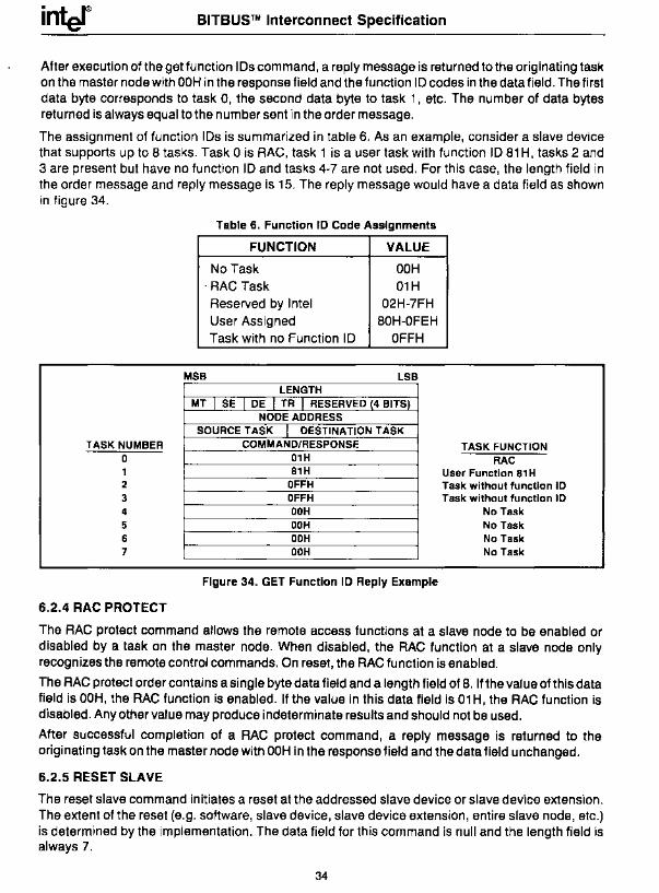
inter BITBUSTM Interconnect Specification
After execution of the get function IDs command, a reply message is returned to the originating task on the master node with OOH in the response field and the function ID codes in the data field. The first data byte corresponds to task 0, the second data byte to task 1, etc. The number of data bytes returned is always equal to the number sent in the order message.
The assignment of function IDs is summarized in table 6. As an example, consider a slave device that supports up to 8 tasks. Task 0 is RAG, task 1 is a user task with function ID 81 H, tasks 2 and 3 are present but have no function ID and tasks 4-7 are not used. For this case, the length field in the order message and reply message is 15. The reply message would have a data field as shown in figure 34.
Table 6. Function 10 Code Assignments
FUNCTION VALUE
No Task OOH -RAG Task 01H Reserved by Intel 02H-7FH User Assigned 80H-OFEH Task with no Function ID OFFH
MSB LSB LENGTH
MT I SET DE I TR T RESERVED (4 BITS) NODE ADDRESS
SOURCE TASK I DESTINATION TASK TASK NUMBER COMMAND/RESPONSE TASK FUNCTION
0 01H RAe 1 81H User Function 81 H 2 OFFH Task without function 10 3 OFFH Task without function 10 4 OOH No Task 5 OOH No Task 6 OOH No Task 7 OOH No Task
Figure 34. GET Function 10 Reply Example
6.2.4 RAC PROTECT
The RAG protect command allows the remote access functions at a slave node to be enabled or disabled by a task on the master node. When disabled, the RAG function at a slave node only recognizes the remote control commands. On reset, the RAG function is enabled.
The RAG protect order contains a single byte data field and a length field of 8. If the value of this data field is OOH, the RAG function is enabled. If the value in this data field is 01 H, the RAG function is disabled. Any other value may produce indeterminate results and should not be used.
After successful completion of a RAG protect command, a reply message is returned to the originating task on the master node with OOH in the response field and the data field unchanged.
6.2.5 RESET SLAVE
The reset slave command initiates a reset at the addressed slave device or slave device extension. The extent of the reset (e.g. software, slave device, slave device extension, entire slave node, etc.) is determined by the implementation. The data field for this command is null and the length field is always 7.
34
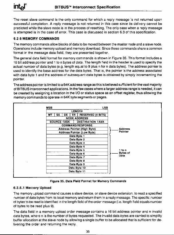
inter BITBUSTM Interconnect Specification
The reset slave command is the only command for which a reply message is not returned upon successful completion. A reply message is not returned in this case since its delivery cannot be predicted while the slave node is in the process of resetting. The only case when a reply message is attempted is in the case of error. This case is discussed in section 6.3 of this specification.
6.2.6 MEMORY COMMANDS
The memory commands allow blocks of data to be moved between the master node and a slave node. Operations include memory upload and memory download. Since these commands share a common format in the message data field, they are presented together.
The general data field format for memory commands is shown in Figure 35. This format includes a 16 bit address pointer and 1 to n bytes of data. The length field in the header is used to specify the actual number of data bytes (e.g. length equal to 9 plus n for n data bytes). The address pointer is used to identify the base address for the data bytes. That is, the pointer is the address associated with data byte 1 and the address of subsequent data bytes is obtained by simply incrementing the pointer.
The address pointer is limited to a 64K address range as this is believed sufficient for the vast majority of BITBUS interconnect applications. In the few cases where a larger address range is needed, it can be created by assigning a location in the I/O or status space as an offset register, thus allowing the memory commands to operate in 64K byte segments or pages.
MSB LSB LENGTH
MT I SE I DE I TR I RESERVED (4 BITSl NODE ADDRESS
SOURCE TASK I DESTINATION TASK COMMAND/RESPONSE
Address Pointer (High Byte) Address Pointer (Low Byte)
Data Byte 1 Data Byte 2 Data Byte 3 Data Byte 4 Data Byte 5 Data Byte 6 Data Byte 7 Data Byte 8 Data Byte 9 Data Byte 10 Data Byte 11
} Address Pointer
1 to n --Bytes of
Data
Figure 35. Data Field Format for Memory Commands
6.2.6.1 Memory Upload
The memory upload command causes a slave device, or slave device extension, to read a specified number of data bytes from its local memory and return them in a reply message. The specific number of bytes to be read is identified in the length field of the order message (Le. length field equals number of bytes to be read plus 9).
The data field in a memory upload order message contains a 16 bit address pointer and n invalid data bytes, where n is the number of bytes requested. The invalid data bytes are carried to simplify buffer allocation at the slave node by allowing a single buffer to be allocated that is sufficient for delivering the order and returning the reply.
35
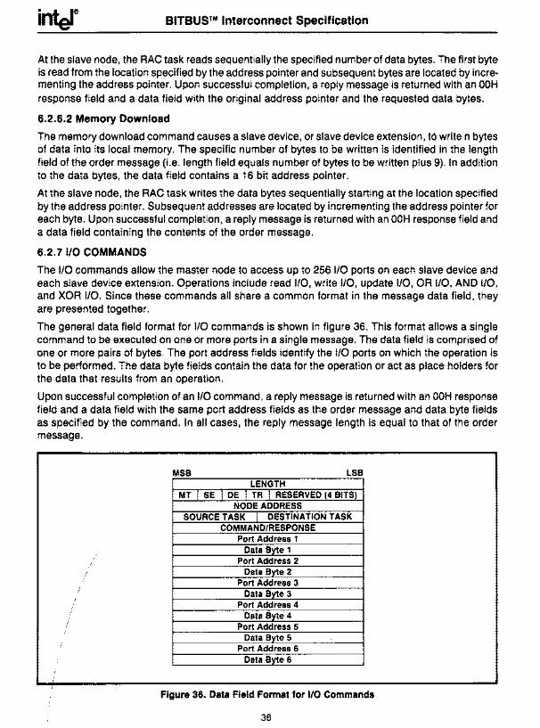
BITBUSTM Interconnect Specification
At the slave node, the RAC task reads sequentially the specified number of data bytes. The first byte is read from the location specified by the address pointer and subsequent bytes are located by incrementing the address pointer. Upon successful completion, a reply message is returned with an OOH response field and a data field with the original address pointer and the requested data bytes.
6.2.6.2 Memory Download
The memory download command causes a slave device, or slave device extension, to write n bytes of data into its local memory. The specific number of bytes to be written is identified in the length field of the order message (Le. length field equals number of bytes to be written plus 9). In addition to the data bytes, the data field contains a 16 bit address pointer.
At the slave node, the RAC task writes the data bytes sequentially starting at the location specified by the address pOinter. Subsequent addresses are located by incrementing the address pOinter for each byte. Upon successful completion, a reply message is returned with an OOH response field and a data field containing the contents of the order message.
6.2.7 1/0 COMMANDS
The 110 commands allow the master node to access up to 256 110 ports on each slave device and each slave device extension. Operations include read 110, write 110, update 110, OR 110, AND 110, and XOR 110. Since these commands all share a common format in the message data field, they are presented together.
The general data field format for 110 commands is shown in figure 36. This format allows a single command to be executed on one or more ports in a single message. The data field is comprised of one or more pairs of bytes. The port address fields identify the 110 ports on which the operation is to be performed. The data byte fields contain the data for the operation or act as place holders for the data that results from an operation.
Upon successful completion of an 110 command, a reply message is returned with an OOH response field and a data field with the same port address fields as the order message and data byte fields as specified by the command. In all cases, the reply message length is equal to that of the order message.
/
/ /
MSB LSB LENGTH
MT I SE I DE I TR I RESERVED (4 BITS) NODE ADDRESS
SOURCE TASK I DESTINATION TASK COMMAND/RESPONSE
Port Address 1 Data Byte 1
Port Address 2 Data Byte 2
Port Address 3 Data Byte 3
Port Address 4 Data Byte 4
Port Address 5 Data Byte 5
Port Address 6 Data Byte 6
Figure 36. Data Field Format for 1/0 Commands
36
inter BITBUSTM Interconnect Specification
6.2.7.1 Read 1/0
The read 110 command causes a slave node to read the specified I/O ports. The data byte fields in the order message are undefined. They are carried only to simplify buffer allocation at the slave node. The data byte fields in the reply message contain the data read from the specified ports.
6.2.7.2 Write 1/0
The write 110 command causes a slave node to write the data bytes fields to the specified 110 ports. The data byte fields in the order message contain the data to be written. The data byte fields in the reply message are unchanged from the order message.
6.2.7.3 Update 1/0
The update 110 command causes a slave node to write the data byte fields to the specified 110 ports, then reread the ports. The data byte fields in the order message contain the data to be written. The data byte fields in the reply message contain the data reread from the 110 port after the write operation.
6.2.7.4 Logical Operations
The logical operation commands provide bit set, bit reset and bit toggle operations. The data byte fields for these operations contain a mask. The command causes the ~Iave node to read the specified 110 port, perform the specified logical operation with the mask in the data byte field, write the result back to the 110 port, then finally reread the port. This final value is entered in the data byte field for the reply message.
Bit operations are defined to logically set, clear and toggle 110 bits. The electrical levels of these operations depends on the implementation. When no signal inversion exists between the internal CPU state and the 110 pin, the operations of set and clear correspond to the electrical high and low states respectively. These implementations are referred to as "active high." If a Signal inversion occurs between the internal CPU state and the 110 pin, the electrical definitions of set and clear are reversed. These implementations are referred to as "active low."
From the logical point of view, bit operations are defined as follows. A bit is set by using an OR 110 command with a one in the bit position to be set. A bit is cleared by using an AND 110 command with a zero in the bit position to be cleared. A bit is toggled by using an XOR 110 command with a one in the bit position to be toggled. Note that it is possible to operate on multiple bits with the same byte in a single operation.
6.2.8 STATUS COMMANDS
The status commands allow the master node to access up to 256 bytes of memory on each slave device and slave device extension. These operations can be used to create a shared data structure between the master and slave nodes. Specific operations include read status and write status. Since these commands share a common format in the message data field, they are presented together.
The general data field format for status commands is shown in figure 37. This format allows a single command to operate on one or more locations with a single message. The data field is comprised of one or more pairs of bytes. The pairs include an address field and a data byte field. The address fields identify the locations at which the operation specified by the command is performed. The data byte field contains the data for the operation or acts as a place holder for the data that results from the operation.
Upon successful completion of a status command, a reply message is returned with an OOH response field and a data field with the same address fields as the order message and data byte fields as specified by the command. In all cases, the reply message length is equal to that of the order message.
37
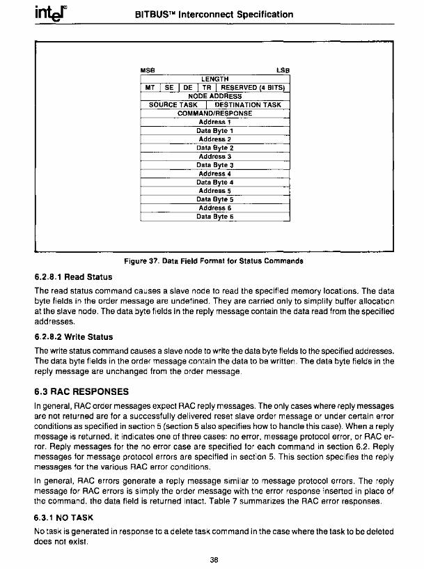
inter BITBUSTM Interconnect Specification
MSB LSB LENGTH
MT 1 SE I DE I TR I RESERVED (4 BITS) NODE ADDRESS
SOURCE TASK I DESTINATION TASK COMMAND/RESPONSE
Address 1 Data Byte 1 Address 2
Data Byte 2 Address 3
Data Byte 3 Address 4
Data Byte 4 Address 5
Data Byte 5 Address 6
Data Byte 6
Figure 37. Data Field Format for Status Commands
6.2.8.1 Read Status
The read status command causes a slave node to read the specified memory locations. The data byte fields in the order message are undefined. They are carried only to simplify buffer allocation at the slave node. The data byte fields in the reply message contain the data read from the specified addresses.
6.2.8.2 Write Status
The write status command causes a slave node to write the data byte fields to the specified addresses. The data byte fields in the order message contain the data to be written. The data byte fields in the reply message are unchanged from the order message.
6.3 RAe RESPONSES
In general, RAG order messages expect RAG reply messages. The only cases where reply messages are not returned are for a successfully delivered reset slave order message or under certain error conditions as specified in section 5 (section 5 also specifies how to handle this case). When a reply message is returned, it indicates one of three cases: no error, message protocol error, or RAG error. Reply messages for the no error case are specified for each command in section 6.2. Reply messages for message protocol errors are specified in section 5. This section specifies the reply messages for the various RAG error conditions.
In general, RAG errors generate a reply message similar to message protocol errors. The reply message for RAG errors is simply the order message with the error response inserted in place of the command. the data field is returned intact. Table 7 summarizes the RAG error responses.
6.3.1 NO TASK
No task is generated in response to a delete task command in the case where the task to be deleted does not exist.
38
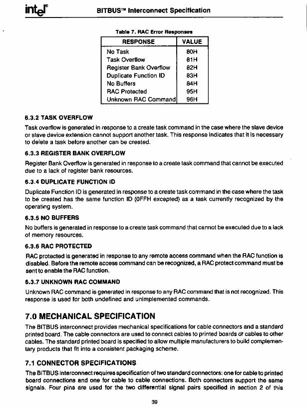
inter BITBUSTM Interconnect Specification
Table 7. RAe Error Responses
RESPONSE VALUE
No Task 80H Task Overflow 81H Register Bank Overflow 82H Duplicate Function ID 83H No Buffers 84H RAC Protected 95H Unknown RAC Command 96H
6.3.2 TASK OVERFLOW
Task overflow is generated in response to a create task command in the case where the slave device or slave device extension cannot support another task. This response indicates that it is necessary to delete a task before another can be created.
6.3.3 REGISTER BANK OVERFLOW
Register Bank Overflow is generated in response to a create task command that cannot be executed due to a lack of register bank resources.
6.3.4 DUPLICATE FUNCTION 10
Duplicate Function ID is generated in response to a create task command in the case where the task to be created has the same function ID (OFFH excepted) as a task currently recognized by the operating system.
6.3.5 NO BUFFERS
No buffers is generated in response to a create task command that cannot be executed due to a lack of memory resources.
6.3.6 RAC PROTECTED
RAC protected is generated in response to any remote access command when the RAC function is disabled. Before the remote access command can be recognized, a RAC protect command must be sent to enable the RAC function.
6.3.7 UNKNOWN RAC COMMAND
Unknown RAC command is generated in response to any RAC command that is not recognized. This response is used for both undefined and unimplemented commands.
7.0 MECHANICAL SPECIFICATION The BITBUS interconnect provides mechanical specifications for cable connectors and a standard printed board. The cable connectors are used to connect cables to printed boards 01' cables to other cables. The standard printed board is specified to allow multiple manufacturers to build complementary products that fit into a consistent packaging scheme.
7.1 CONNECTOR SPECIFICATIONS
The BITBUS interconnect requires specification of two standard connectors: one for cable to printed board connections and one for cable to cable connections. Both connectors support the same signals. Four pins are used for the two differential signal pairs specified in section 2 of this
39
inter BITBUSTM Interconnect Specification
specification for the BITBUS interconnect. Four additional pins are provided for power distribution to low power nodes. Finally a high impedance ground (100 ohms to ground) is provided as specified in the RS485 specification (not required in all implementations). Figure 38 and 39 show the two connectors and table 8 lists the pin assignments.
4 EQUAL SPACES AT (2'5411_1 • _I I'
.100 1 .
A ' 1
1 1
1 ..... e--__ (27,941 1.10
POSITION 1
--1- T - _ (3,81) (7,371 ___ .15
.29 2 PL
TQPY'EW
(7,621
.~J
(8,091 .24
-~ (3,8~±,251 .155' .010
SECTIONA.A
NOTE: PINS MAY BE STRAIGHT OR AT 90% ANGLE DEPENDING ON APPLICATION,
Figure 38. Printed Board Connector
Table 8. Connector Pin Assignments
SIGNAL PRINTED BOARD CABLE CONNECTOR CONNECTOR PIN # PIN #
+12V±5% 1 1 + 12V±5% 2 6 GND 3 2 GND 4 7 DATA * 5 3 DATA 6 8 DCLK* IRTS* 7 4 DCLKlRTS 8 9 RGND (100 ohms to GND) 9,10 5
40
inter BITBUSTM Interconnect Specification
(12.52 ± .25) .493±.010
1+-__ (30.89± .25) __ .-j 1.216±.010
.)SOCKET
~ __ (30.89±.25) __ ..... 1.216t·Ol0
b) PLUG
(3.18±.25) .125 ± .010 RAD. TYP.
(2.84) .112
(3.12±.05) DIA .123±.002
(1.52±.13) RAD TYP .060±.005 . .
(2.84) .112
(3.12 ± .05) DIA .123t·002
Figure 39. Cable to Cable Connector
The standard cable to printed board connector is a 10 pin latching pin and socket type with strain reliefs. This connector can support either flat cable or discrete wire connection.
The standard cable to cable connector is a 9 pin O-subminiature type. Versions of this connector are also available for flat cable or discrete wire connection.
7.2110 BOARD SPECIFICATION
The BITBUS I/O board is designed to be compatible with the single-high Multibus II board form factor. This definition is based on the International Electrotechnical Commission (IEC) standards. This section provides an overview of the mechanical dimensions of this board and presents standard pin assignments. For further details (e.g. board spacing, component height, ejector tabs, front panels, etc.) refer to the Mechanical Specification in the Multibus II Bus Architecture Specification.
7.2.1 BOARD DIMENSIONS
Figure 40 shows the board dimensions for the standard BITBUS I/O board. This board is a standard single-high, 220mm deep form factor.
41
inter BITBUS™ Interconnect Specification
c w
5ffi OoU ZC 0'" zOo
c:: is
'I $
w c iii .... z w z o Oo
~ U
Figure 40. Standard Board Dimensions
42
t ,t + ~'Jil------~_A_
OPTIONAL DATUM HOLE
OPTIONAL TOOLING HOLE
7.850 @, (18.,31)
'·IL=t:ci~~:.)-§!!] ,J ',_MP
II: Oz .. 0"
iO~=I5::i. !!Ie~~g 12gf5!!E '~~~i!N UOO OU Z
1651
inter BITBUSTWI Interconnect Specification
7.2.2 CONNECTORS
The BITBUS I/O boards use two piece, 64-pin connectors. Figure 41 and 42 show the dimensional specification for the connectors. The right angle connectors on the printed board are IEC standard 603-2-IEC-C064-M; the receptacle connectors are IEC standard 603-2-IEC-C064-F. Figure 43 shows the relationship between connectors and boards in a subrack. Note that compatible recepticle connectors are available for flat cable, discrete wire or wire wrap connections in addition to the backplane version shown.
.100
(:~:~, f ~~100
~1r- ~ .114 I I
I ':~; 111-- -l~ ~ (;~~:, t~A -----,--I MAX. ""1 t ir- 3.543±.004
D.::~+:'~P 1_ -- (90±0,101 COflt<~1~~NI CENTERS TYPICAL
;~:~j r=== __ ~~~....:t~.~~~~,-----~~~~~ __ .~~ TYP. (951 ---1
(4,831
Figure 41. Board Connector
(~~5~~ 1_~~~~~ __ ~.o'.3.~50~0:=±~.00~4~~~~~~ __ DIA. TYP, " (88.90±O,10)
• .437 MA:=II~ : :: ====::-(11,11 _______ _
t _~~~~ __ _
TYPICAL
PINSON "00/(2'541-1 SPACING
3.700 MAX. (84,001
-------111 ----------------
__ ~~n Figure 42. Backplane Connector
43
NOTE: CENTER ROW OF CONTACTS NOT INSTALLED
.100 TYP.
__ t_ ~
~[!; (0,641
NOTE: CENTER ROW OF CONTACTS NOT INSTALLED
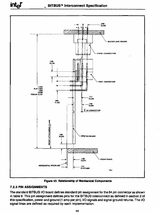
inter
f
+.03. 8.21+.03.
-.008 +0,88
(235,2.-0,1.)
" BITBUSTM Interconnect Specification
.108
'Ll--~~ f--~
1-.300 (7,82)
.171 (.,35)
BACKPLANE BOARD
FREE CONNECTOR
i. OF CONNECTOR
PRINTED BOARD
,
t ·128 (3,27)
.121 (3.07) REF.
FRONT PANEL
1641
Figure 43. Relationship of Mechanical Components
7.2.3 PIN ASSIGNMENTS
The standard BITBUS 1/0 board defines standard pin assignment for the 64 pin connector as shown in table 9. This pin assignment defines pins for the BITBUS interconnect as defined in section 2 of this specification, power and ground (1 amp per pin), 1/0 signals and signal ground returns. The 1/0 signal lines are defined as required by each implementation.
44
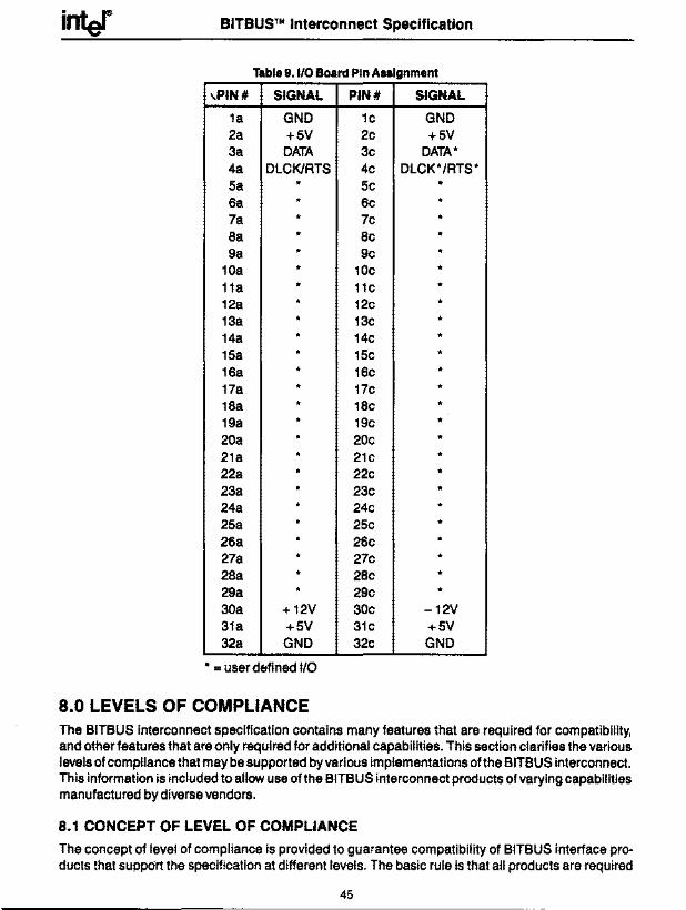
BITBUSTM Interconnect Specification
Table 9. I/O Board Pin Assignment
,PIN # SIGNAL PIN# SIGNAL
1a GND 1c GND 2a +5V 2c +5V 3a DATA 3c DATA* 4a DLCKJRTS 4c DLCK*/RTS* 5a * 5c * 6a * 6c * 7a * 7c * Ba * Bc * 9a * 9c *
10a * 10c * 11a * 11c * 12a * 12c * 13a * 13c * 14a * 14c * 15a * 15c * 16a * 16c * 17a * 17c * 1Ba * 1Bc * 19a * 19c * 20a * 20c * 21a * 21c * 22a * 22c * 23a * 23c * 24a * 24c * 25a * 25c * 26a * 26c * 27a * 27c * 2Ba * 2Bc * 29a * 29c * 30a +12V 30c -12V 31a +5V 31c +5V 32a GND 32c GND
* = user defined I/O
8.0 LEVELS OF COMPLIANCE The BITBUS interconnect specification contains many features that are required for compatibility, and other features that are only required for additional capabilities. This section clarifies the various levels of compliance that may be supported byvarious implementations of the BITBUS interconnect. This information is included to allow use of the BITBUS interconnect products of varying capabilities manufactured by diverse vendors.
8.1 CONCEPT OF LEVEL OF COMPLIANCE
The concept of level of compliance is provided to guarantee compatibility of BITBUS interface products that support the specification at different levels. The basic rule is that all products are required
45
inter BITBUS™ Interconnect Specification
to support a minimum level of the specification. This results in a minimal level at which all BITBUS interconnect products can interact. Furthermore, enhancements beyond this minimal level are controlled. This results in a guaranteed compatibility between a group of products that all support the same enhanced capabilities. -
8_2 COMPLIANCE LEVELS
This section presents the various levels of compliance for each level of the specification. Each capability supported beyond the minimum shall be documented in the product data sheet.
8.2.1 ELECTRICAL INTERFACE
The electrical interface supports variability in bit rates, load characteristics, and repeater characteristics. The bit rates specified in section 2 include 2.4 Mbits/sec synchronous and 375 kbits/sec and 62.5 kbits/sec self clocked. Ofthese only 375 kbits/sec is required. The others may be optionally supported. The load for a BITBUS node shall be specified in terms ofthe standard load defined in section 3.2.1. Repeaters are specified in terms of the standard repeater delays defined in section 3.3.5.
8.2.2 DATA LINK PROTOCOL
The data link protocol has no optional features. The full protocol shall be supported for compatibility.
8.2.3 MESSAGE PROTOCOL
The message protocol supports variability in message length. All implementations shall support the standard 5 byte header and 13 byte data field. Implementations may optionally support larger data fields.
8.2.4 REMOTE ACCESS AND CONTROL
Support of the remote access and control function is completely optional. The only requirement is that supported commands shall meet the specification.
8.2.5 MECHANICAL
The mechanical specification contains the option of supporting the standard 110 board specification. As wit" RAG, the only requirement is that if supported, it shall meet the specification.
46

inter 'UITft.WA
CtlNA/HOHGi KONG
_.1IT1IIA DAFSYSS.R.L Chacabuoo, 80-<4 ABO 1 oat-Buenoa AIret r":54-1-334-1871
54-' ...... 7720 TLX: 25472
AUITIWJA
TotaIEJectronICs 15--17 HumeSIrMt HuntingdaII,31116. ~.AUltraliI Tel: 03-544-8244 TlX: AA 30885 FAX: 03-544-8179 ...... ..... -
INTERNATIONAL SALES OFFICES
JAPAN
~~~~~iBIdg. 1·~ Shlnmachl
~~~'54 FAX: 03-427-7820
Intel Japan K.K.·
rJB·.=ya ~~~360 FAX: 0485-24-7518
=.~':;:.....-..... ..... 915 Shlnmaruko, Nakahara..J(u Kawaaakl-thl. Kanagawa 211 Tel: 044-733-1011 FAX: 044-733-7010
INTERNATIONAL DISTRIBUTORS/REPRESENTATIVES
'''''' MICronIcDevIces
~65~J'cT.'Roact
JAPAN (Cont'd.)
Dia_~_.lnc.
=:tw~T~~jay, Tel: (J3:487-0388 FAX: 03-487-8088
~~ ~~IlSfl:t'I480 FAX: 052-204-2901
Ryoyo Electro Corp, ........... 1-12-22T~
¥~~s4=,'04 FAX:~
K .....
J-Tek~
~~PenalonBidg. ~nn;ngpo. u Tel: 82-2-782-8039
A. o.r.Ido FIIuIInI aon., 78 TLX: 25299 KOOtGIT 8_ 04875 - s.o Paulo - S.P. Tel: 011-65-11-534-1131 TLX: .,1t25t31 ELBA SA FAX:55-11..&34-9424 .....
...... N
FAX: 82-2-784-8391
~Semlconcluctora TeIecommunlcltlons Co., Ltd. ~;~, Tafpyung-ro, Chuog-ku
Tel: 82-2-751-3987 TLX: 27970 KORSST FAX: 82-2·753-0987
... lOCO
"-S .•. TocMII3e8 Frace. Ind. San AntonIo
~==.D.F. TLX: 1n3790 DtCOME
Printed in England by Carlton Barclayl1088/2K
KORI!A
TAIWAN
IntelT~(F ... EI,t) Ltd. Taiwan BranctI '~F, NO. 205, Tun Hull N. Road
~"~2~j~6-1MMIO TLX: 13159INTELlWN FAX: 886-2·717·2455
-.........., SwItch_ ... 36 Olive Road Penrose. Auckland, ATTN: Dean Dlnford Tel: 64-9-591155, FAX: 84-9-592081 ............
sount APRICA
~=IngElttmentl,Ply.Ltd.
Pine Square, 18th StrNt Hazetwood, Pretoria 0001 Tel: 27-12-488121 TLX, 3-227788" FAX~ 0927-012-.48-8221
TAIWAN
~~~=.n~ ~=~~1-3231 FAX: 888-2-501~
VENIZUILA

intJ DENMARK
''''''' Glenl8Ve161,3rdFIoor 2400 Copenhagen NV Tel: (01) 1980 33 Telb 19567
FINLAND
,-Ruosdanlle2 00390 HalslOlu TeI-t3580644644 Telex 123332
FRANCE
Inl81 1, rue EdillOn - BP 303 78064 5t Quenlln-en-Yvehnes Cedel( T81:(1)30571Ooo Tetell,899018
""., 4, Qual des EtrOl1s 89321 Lvon Cede. 06 Tal. 78424089 T .... 306153
EUROPEAN SALES OFFICES
NETHERLANDS
'mol Marten Meesweg 93 3068AVRotterdim Tel: (31)-(0)10-421.23.77 Telex 22283
ISRAEL
'niel Atidlm Industrial Peril-Neva sneree P.O.8oIt43202 Tel-AvIV 61430 Tel: 03-498080 Telux" 371215
JTALV
''''''' Milanofiori Palazzo E 20090_ Miktno rei: (02) 824 40 71 TeIax.341286
NORWAY
,,101 Hvamveien 4 - PO b 92 2013Skjetten Tel: (8)842 420 TeIu: 78018
SPAIN
'nIOI Zurberan,28 28010MadrKl 1&1.4104004 Telex, 46880
SWEDEN
'nIOI ~~SJ!' TeI:t4687340100 1e1811.12261
SWfTZERLAND
''''''' Telacun51Jasse17 8066Zunctl rei: 01 1829 29 77 Telex 57989
U.K.
''''''' PipersWwv Swindon, Wilts SN3 lRJ Tel. (0793)696000 181811. 44444718
WEST GERMANY
,-Oornacher SlrMSe 1 8016 Fekl'.lrchen bel MUnche!'l rei. (()89)909920 Telex 5-23177
, ... , Hohenmllern Sirasse 5 3OOOHal"ll'lOYef 1 Tel 1061')344081 TeIeJt 9·23626
, ... , Abraham lincoln Sirane 16·18 6200 Wlesbaden Tel (O6121)7806"() T"'.:4·168183
Inlel ZattachringlOA.
~~\~ro TeIeJt: 7·254826
EUROPEAN DISTRIBUTORS/REPRESENTATIVES AUITRIA
Bacher EllICtfonlcl G,m.b.H Ro!enmuhlg .... 26 11lOWlen Tel' (0222)83 66 46"() TeIeJt.131632
IELGIUM
InalDo BelgIum SA Av. del Crot. de Guerre 94 1120 BrUltell ..
?r~=nlaan. 94
rei. (02)216 01 60 releJt' 64476
DENMARK
m·Mulllkompopnent Haverland 29 2600GlosIrup rei' 46 (0) 2 45 6646 TeleJt 333&6
fiNLAND
ov FlnlranlC AS Melkonkalu24A 00210 Helllniu Tel, 10189215022 Telp 124224
FRANCE
GlIM1'lm l.A. de Courtaboeuf Av. de la BIIhqU8 - BP 88 91943 Le. UII. Cedelt rei: (1)6907 78 78 Telp, 691700
Mlkrologle Tourd'Aanltres 4,8V.uurent·CeIy 92808 Alnitrft CedeJt Tel: (1)47908240 Tele.611448
Teket.c·A!rtronlC Rue Cerle·Ve"'" - BP 2 92316 SMes Cede. Tel (1)45347535 Tele.· 204662
IRELAND
Micro Mllfketlng Ud Glenegeary Office Perk
&,~ry rel:(01)856325 rele •. 31684
.RAEL
EnlroniCl Ud. 11 RONnI,S1. P.O,B. 39300 rel·AvlV 61392 Tel: 03-476151 T",33638
ITALY ,-OiYiIione m loduatnes GmbH VlaleMilenoflOl'i PalauoE/6
~~~MI) Tele., 311351
~~ ~=:r~i~f~' 20092 Clnisallo Balsamo (Mt) Tel: 02/2440012 relax: 3G2040
NETHERLANDS
NORWAY
Nordllk Eleltlronlkk (Norlt8) AlS PoetbokI123
=''r~4 rei: (02)84 82 10 releJt' n548
PORTUGAL
Dlttam AWlnidII MerquN de Tomar, 46·A l000Lilboe r":(1)734834 TeIelt'14182
SPAtN
ATO EleclronlCll, S.A Pled Cluded de Vlena. 6 28040 Madrid rei: 2344000 rele.·42754
ITT·SESA ~~~~::nv-I, 21·3
TeI,4190957 TeleJt:27461
SWEDEN
Nardilk Elaililronlk AS HUllUdltagatltn 1 ""409 17127Solna Tel. 08·734 97 70 Telax: 10647
SWITZERLAND
InduatradllA.G. Haniltfa ... 31 B31)4WaIliMlIan Tel: (801)83 06 04 0 Tele.: 56788
TURKEY
EMPAElectronic Lindwurm.lr .... 95A BOOO MUnchen 2 Tel: 089/63 80 570 Telax:628ti73
UNITED KINGDOM
AccenI Eleclronic Component. Ud ,Jubilee House ,Jubi1 .. RoecI loIct>wonh HertsSG61TL Tel: (0462)686666 TeleJt.826293
Bvtech·Comway Syatema 3 The w..twn Cent ... Weltern Road Brecknall RG12 lRW Tel, f(344)66333 Te"':847201
Jo<myn V_ryE ....
""""''''''''' ........... Ken! TN14 5EU Tel. (0732)460144 TeleJt' 95142
MMD Uni' 8 SouttIView Pan:
""""""'" .... ,"" BerkshireRG40AF rei: (07341481666 releJt 846669
Rapid System. . .... -Denme"rk Street High Wycombe Buc:ltinghamshlre HP11 2ER rei: (0494)450244 rele.:837931
Rapid SIlicon Rapid Houae DenmerkStf"eet High W;cornbe BooIunghamlhlre HP11 2ER Tel: (0494)442266 TeIeJt. 837931
WEST GERMANY
EleclronK:2000AG
='t~~ Tel: f089l42001-O T .... 622581
ITT Multdcomponent GmbH PoItfech 1286 Behnhofltr .... 44
~~~~~~=.347 Te"', 7264399
Jermyn GmbH 1m DactllICuck 9
~~~.() Te'" 4Hi257..()
Metrolog .. GmbH
=i~~:9 Tel' (Cl89)78042"() Te"', 5213189
Proelec:tronV.uiebaGmbH MIIlIPlanc:ltStr .... ,·3 8072 OJeteich Tel. 06103/304343 r .... :417972
VUGOSLAVIA
H,R. MlCroeleclrontCl Corp. 200& de la Cruz Bhtd. Suite 223 Santa C ...... CA 96060 U.S.A rei: (408I8B8 0286 Tele.: 387452
Eu1'Ql1107l88


