Scientific Journal Impact Factor (SJIF): 1.711 International Journal of Modern Trends in Engineering and Research www.ijmter.com @IJMTER-2014, All rights Reserved 524 e-ISSN: 2349-9745 p-ISSN: 2393-8161 ANALYSIS OF SOLID STATE TRANSFORMER WITH PERMANENT MAGNET SYNCHRONOUS GENERATOR Geetha. K 1 , Venkatesan. P 2 1 PG Scholar, Department of EEE, Vivekananda College of Engineering for Women 2 Asst.Professor,Department of EEE, Vivekananda College of Engineering for Women Abstract- In recent years the complexity of the grid systems has grown due to the increased penetration of renewable energy and distributed generation sources. The increased complexity requires new methods to quickly manage the changing sources and loads. This research focuses on one of such technologies, called the SST. A SST uses power electronic devices to achieve voltage conversion from one level to another. Several SST topologies have been proposed by different research groups, without a clear idea on which is most suited for grid applications.To ensure a proper choice of topology,a separate literature review is presented in this paper. The final choice of topology is extremely modular. In this, conventional dc-dc converter of solid state transformer is replaced by SEPIC converter and the analysis is done using PMSG. Keywords-Solid StateTransformer (SST); single ended primary inductance converter (SEPIC); permanent magnet synchronous generator (PMSG); topology; voltage conversion I. INTRODUCTION In recent years, the complexity of the electrical grid has grown due to the increased use of renewable energy and other distributed generation sources. To cope with this complexity, new technologies are required for better control and a more reliable operation of the grid. One of such technologies is the solid-state transformer (SST). The SST technology is quite new and therefore the knowledge on the behavior of these systems in the grid is rather limited. In the present power grids, energy is generated in large power stations and transmitted over high voltage lines. This energy is then delivered to consumers via medium and low-voltage lines. In these grid layouts, the power flow goes only in one direction: from central power stations to consumers[1]. In recent years, many European countries have started to liberalize their electricity market. This liberalization brought with it an increased penetration of renewable energy and other distributed generation sources in the grid. These developments cause the network layout and operation to become much more complex. In order to better manage future grids, sometimes also called smart grids, new technologies are required that allow better control, an increased number of power inputs and bi-directional power flow. A key enabler for smart grids is the solid-state transformer. The SST offers ways to control the routing of electricity and provides flexible methods for interfacing distributed generation with the grid. The solid-state transformer also allows for control of the power flow, which is needed to ensure a stable and secure operation of the grid. However, this comes at the cost of a more complex and expensive system.
Transcript
Scientific Journal Impact Factor (SJIF): 1.711
International Journal of Modern Trends in Engineering
and Research www.ijmter.com
@IJMTER-2014, All rights Reserved 524
e-ISSN: 2349-9745
p-ISSN: 2393-8161
ANALYSIS OF SOLID STATE TRANSFORMER WITH PERMANENT
MAGNET SYNCHRONOUS GENERATOR
Geetha. K1, Venkatesan. P
2
1PG Scholar, Department of EEE, Vivekananda College of Engineering for Women 2Asst.Professor,Department of EEE, Vivekananda College of Engineering for Women
Abstract- In recent years the complexity of the grid systems has grown due to the increased
penetration of renewable energy and distributed generation sources. The increased complexity
requires new methods to quickly manage the changing sources and loads. This research focuses
on one of such technologies, called the SST. A SST uses power electronic devices to achieve
voltage conversion from one level to another. Several SST topologies have been proposed by
different research groups, without a clear idea on which is most suited for grid applications.To
ensure a proper choice of topology,a separate literature review is presented in this paper. The final
choice of topology is extremely modular. In this, conventional dc-dc converter of solid state
transformer is replaced by SEPIC converter and the analysis is done using PMSG.
Keywords-Solid StateTransformer (SST); single ended primary inductance converter (SEPIC);
permanent magnet synchronous generator (PMSG); topology; voltage conversion
I. INTRODUCTION
In recent years, the complexity of the electrical grid has grown due to the increased use of
renewable energy and other distributed generation sources. To cope with this complexity, new
technologies are required for better control and a more reliable operation of the grid. One of
such technologies is the solid-state transformer (SST). The SST technology is quite new and
therefore the knowledge on the behavior of these systems in the grid is rather limited.
In the present power grids, energy is generated in large power stations and transmitted over high
voltage lines. This energy is then delivered to consumers via medium and low-voltage lines. In
these grid layouts, the power flow goes only in one direction: from central power stations to
consumers[1]. In recent years, many European countries have started to liberalize their electricity
market. This liberalization brought with it an increased penetration of renewable energy and
other distributed generation sources in the grid. These developments cause the network layout
and operation to become much more complex. In order to better manage future grids,
sometimes also called smart grids, new technologies are required that allow better control, an
increased number of power inputs and bi-directional power flow.
A key enabler for smart grids is the solid-state transformer. The SST offers ways to control
the routing of electricity and provides flexible methods for interfacing distributed generation
with the grid. The solid-state transformer also allows for control of the power flow, which is
needed to ensure a stable and secure operation of the grid. However, this comes at the cost of
a more complex and expensive system.
International Journal of Modern Trends in Engineering and Research (IJMTER)

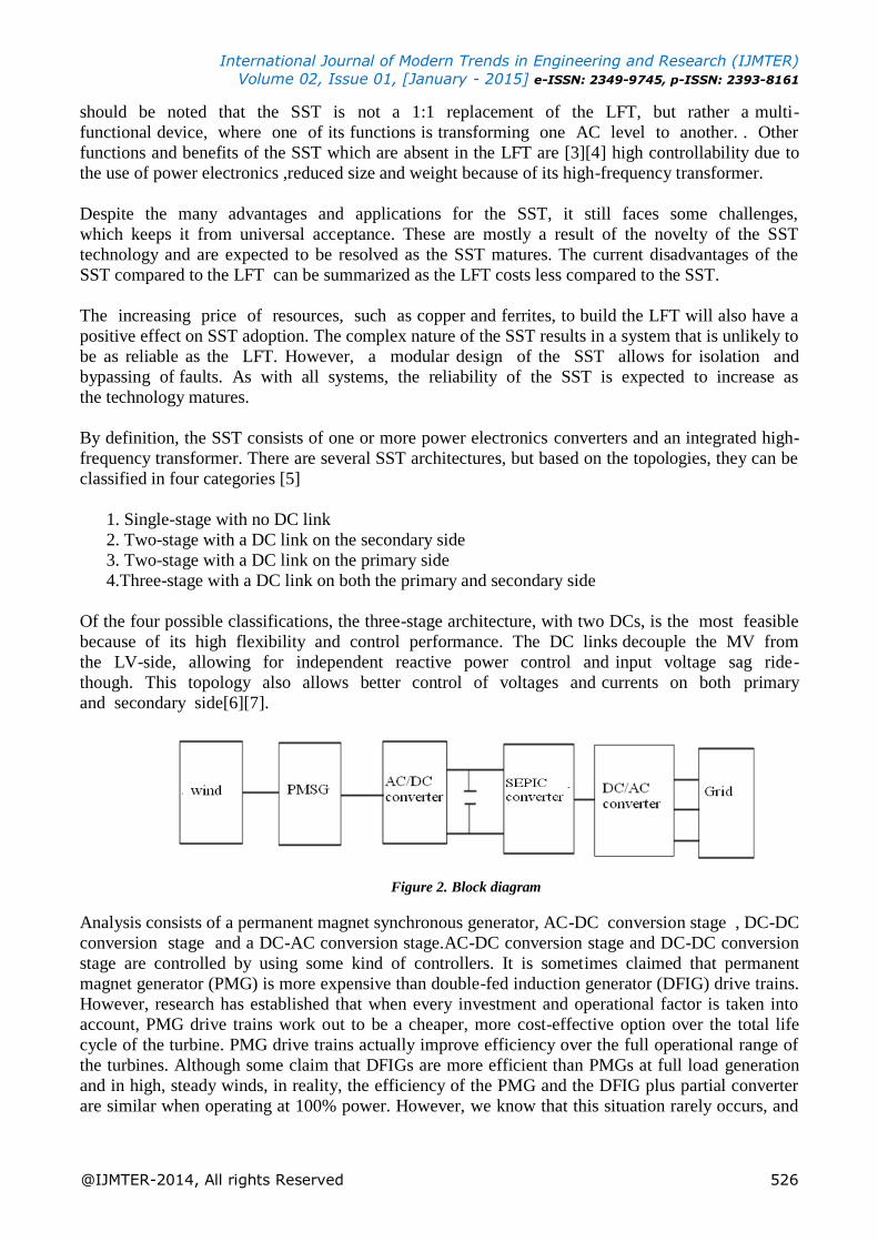


![[5]the Age of Multilevel Converters Arrives](https://static.documents.pub/doc/80x56/553318214a795998578b47e1/5the-age-of-multilevel-converters-arrives.jpg)


