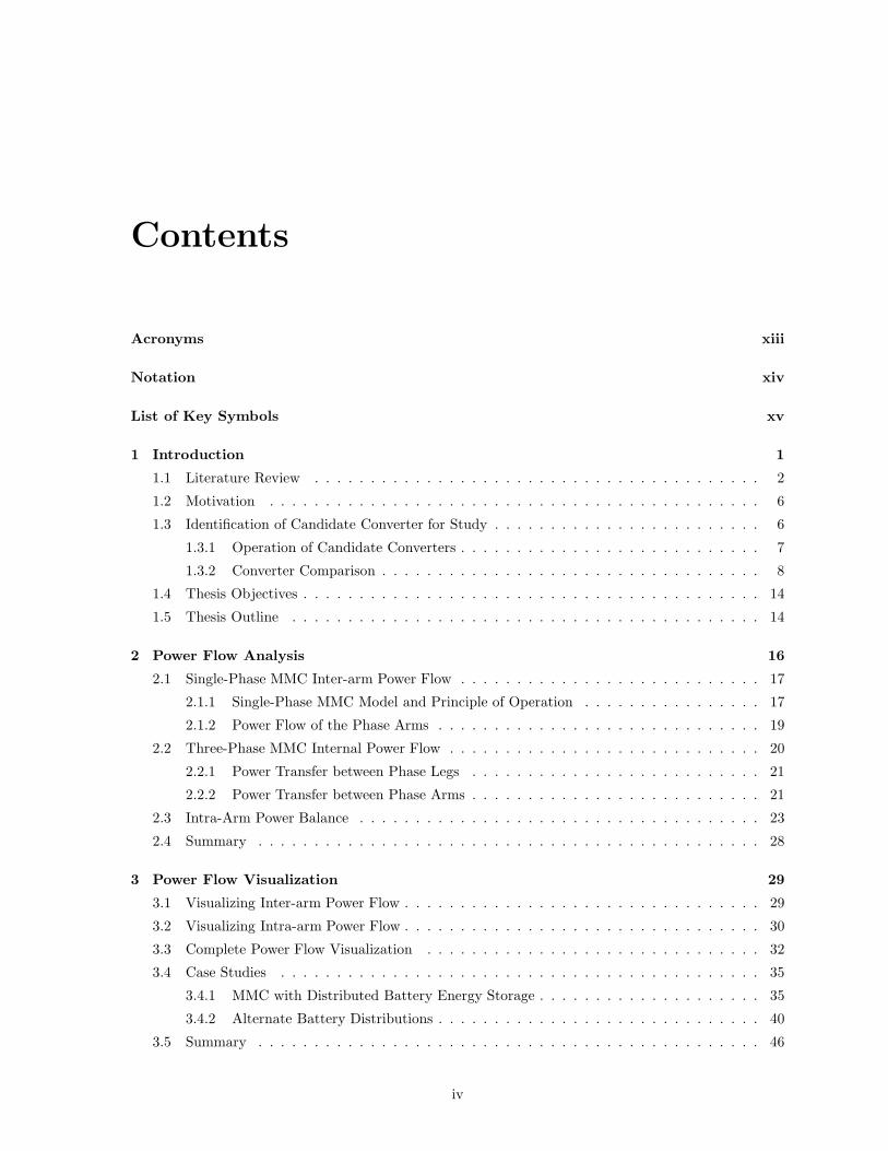
Switch Type (1.2kV / 0.9kA IGBT)Rated Submodule Capacitor
0.6kVVoltage (Vnom,SM )
Rated Submodule Peak Current 1.4kA
Table 1.2: Switch Loss ParametersSwitch Type FF1400R12IP4 FF900R12IE4T
Saturation Voltage (VCE,sat) 0.85 V 0.85 VOn Impedance (Ron) 0.943 mΩ 1.4 mΩFixed Energy Loss Per
64.7 mJ 13.5 mJPulse (On And Off) (Etot,fixed)
Variable Energy Loss Per0.224 mJ/A 0.265 mJ/A
Pulse (On And Off) (Etot,var)
Table 1.3: Converter Parameters
Converter AttributeMMC with MMC with
CascadedCentralized DistributedBES BES
Prated 33.2 MW 47.4 MW 23.7 MWRated Average SM Current 0.68 kA 0.89 kA 0.89Rated Peak SM Current 1.4 kApk 1.4 kApk 1.4 kApk
Modules per Phase Leg 126 (Half Bridge SM) 88 (Half Bridge SM) 22 (Full Bridge SM)Installed Switch MVA
423.4 485.8 195.4per Phase Leg
Installed Switch MVA 12.8 10.2 8.2per MW output
Chapter 1. Introduction 12
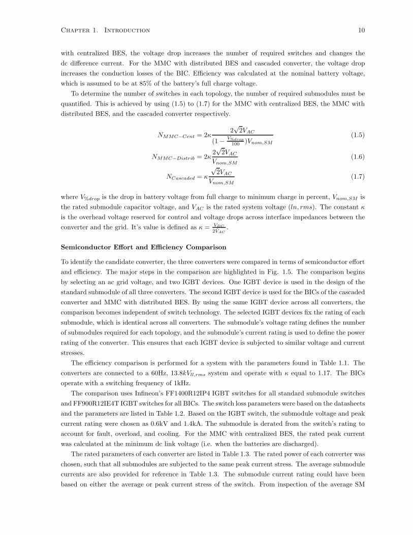
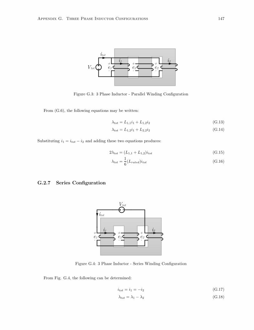
Define VAC
Define Standard Submodule
Switch
Define BIC Switch
MMC with Centralized BES
Cascaded andMMC with
Distributed BES
# Modules
VACVBAT,max
VBAT,min
# ModulesVAC
Find Prated at Peak Switch
Current
Find Prated at Peak Switch
Current
Calculate Efficiency and Semiconductor
Effort
Figure 1.5: Overview of the semiconductor effort and efficiency comparison process.
currents, the average submodule current is higher for the MMC with distributed BES and cascaded
converters compared to the MMC with centralized BES. This would imply that the switches are being
more heavily stressed in the MMC with distributed BES. However, when looking at the efficiency of
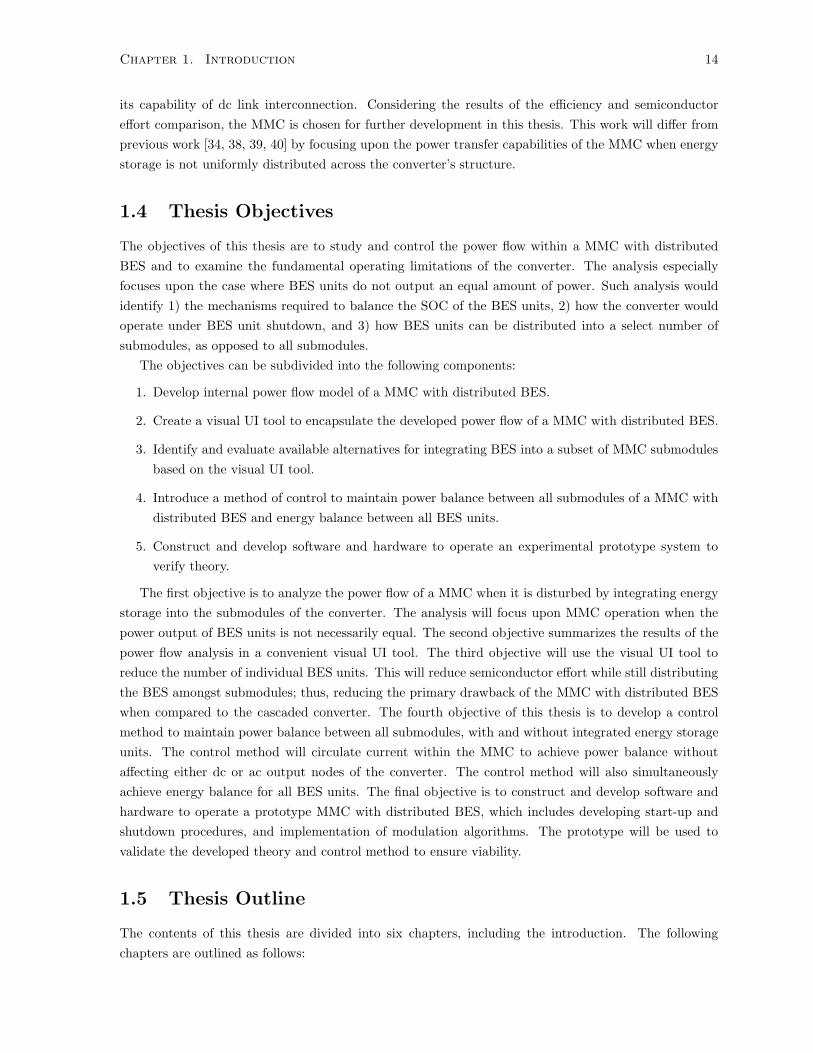
the entire converter, shown in Fig. 1.6, the MMC with distributed BES and cascaded converter have
higher efficiency compared to that of the MMC with centralized BES. This implies that the thermal
requirements of the MMC with distributed BES and cascaded converter are easier to manage, and the
switches are not actually overstressed when the peak current is used to rate the submodule.
From the efficiency curves of Fig. 1.6, the MMC with distributed BES is shown to be the most
efficient, followed by the cascaded converter, and then the MMC with centralized BES. The difference in
efficiency between the MMC with centralized BES and the MMC with distributed BES can be attributed
to the current that each module must conduct. As discussed in Section 1.3.1, the MMC with distributed
energy storage does not need to transfer power from the dc link to the converter. Therefore, the converter
arms do not need to conduct a dc current, whereas the MMC with centralized BES does.
In Table 1.3, the semiconductor effort of the converter was measured with the “Installed Switch MVA
per MW output” ratio. The ratio is computed by summing the switch VA of the BICs and DC/AC
converter switches, and dividing it by Prated. While the MMC with distributed BES is the most efficient
topology, it has a higher semiconductor effort when compared to the cascaded converter. In addition,
the MMC with centralized BES has the highest semiconductor effort and lowest efficiency, and is the
least preferred option. Comparing the two MMC variants, contrary to intuition, the addition of the BICs
enhances efficiency and ultimately reduces the semiconductor effort, for the same Prated. The presence
of the dc current in the MMC with centralized batteries decreased efficiency, and derated the output
power of the topology. Evidently, the dc current has a higher impact on semiconductor effort than the
addition of the BICs.
Chapter 1. Introduction 13
0 0.2 0.4 0.6 0.8 198.5
98.6
98.7
98.8
98.9
99.0
99.1
99.2
99.3
99.4Efficiency Comparison
Power (p.u.)
Efficien
cy(%
)
MMC with Centralized BESMMC with Distributed BESCascaded Converter
Figure 1.6: Comparison of efficiency between MMC with distributed BES, MMC with centralized BES,and cascaded converter.
Redundancy
This section focuses on the issue of reliability for BES systems, especially focusing upon redundancy for
the candidate converters. As previously noted, the MMC with centralized BES does not have increased
redundancy compared to existing systems. However, this is not the case for the MMC with distributed
energy storage, nor for the cascaded converter, which both subdivide the BES into shorter strings.
For the cascaded converter utilized as part of a BES system, it has been shown by [31] that power can
be independently delivered to each submodule. This method would produce a zero sequence voltage at
the ac terminals of the cascaded converter. Reference [49] also demonstrated that a cascaded converter
is able to deliver limited active power when a single submodule of each phase leg is connected to a dc
source, but as of writing, operation of the cascaded converter with an arbitrary number of integrated
sources is still an open research question. Thus, redundant modules may be required to address battery
failures.
In contrast, the MMC with distributed energy resources offers more flexibility and redundancy than
the cascaded converter. Work presented in [35] showed that submodules can operate with some modules
that do not provide any real power, which is achieved without impacting MMC operation. This implies
that energy storage is not required in all submodules of the converter and a MMC with distributed BES
can be built with both standard and energy storage submodules to reduce semiconductor effort and
complexity.
In addition, the existence of a fixed dc link in the topology provides two advantages. First, the dc
link allows power transfer between phases, which can potentially be achieved without affecting either dc
or ac terminals of the converter. Secondly, the fixed dc link allows the BES system to be integrated into
a dc network without any additional complexity. Thus, the MMC can offer redundancy and versatility
beyond that of the cascaded converter due to independent power delivery from any submodule and
Chapter 1. Introduction 14
its capability of dc link interconnection. Considering the results of the efficiency and semiconductor
effort comparison, the MMC is chosen for further development in this thesis. This work will differ from
previous work [34, 38, 39, 40] by focusing upon the power transfer capabilities of the MMC when energy
storage is not uniformly distributed across the converter’s structure.
1.4 Thesis Objectives
The objectives of this thesis are to study and control the power flow within a MMC with distributed
BES and to examine the fundamental operating limitations of the converter. The analysis especially
focuses upon the case where BES units do not output an equal amount of power. Such analysis would
identify 1) the mechanisms required to balance the SOC of the BES units, 2) how the converter would
operate under BES unit shutdown, and 3) how BES units can be distributed into a select number of
submodules, as opposed to all submodules.
The objectives can be subdivided into the following components:
1. Develop internal power flow model of a MMC with distributed BES.
2. Create a visual UI tool to encapsulate the developed power flow of a MMC with distributed BES.
3. Identify and evaluate available alternatives for integrating BES into a subset of MMC submodules
based on the visual UI tool.
4. Introduce a method of control to maintain power balance between all submodules of a MMC with
distributed BES and energy balance between all BES units.
5. Construct and develop software and hardware to operate an experimental prototype system to
verify theory.
The first objective is to analyze the power flow of a MMC when it is disturbed by integrating energy
storage into the submodules of the converter. The analysis will focus upon MMC operation when the
power output of BES units is not necessarily equal. The second objective summarizes the results of the
power flow analysis in a convenient visual UI tool. The third objective will use the visual UI tool to
reduce the number of individual BES units. This will reduce semiconductor effort while still distributing
the BES amongst submodules; thus, reducing the primary drawback of the MMC with distributed BES
when compared to the cascaded converter. The fourth objective of this thesis is to develop a control
method to maintain power balance between all submodules, with and without integrated energy storage
units. The control method will circulate current within the MMC to achieve power balance without
affecting either dc or ac output nodes of the converter. The control method will also simultaneously
achieve energy balance for all BES units. The final objective is to construct and develop software and
hardware to operate a prototype MMC with distributed BES, which includes developing start-up and
shutdown procedures, and implementation of modulation algorithms. The prototype will be used to
validate the developed theory and control method to ensure viability.
1.5 Thesis Outline
The contents of this thesis are divided into six chapters, including the introduction. The following
chapters are outlined as follows:
Chapter 1. Introduction 15
Chapter 2 presents the power flow analysis of the MMC with distributed BES.
Chapter 3 presents a visual tool, used to convey the power flow analysis.
Chapter 4 presents the developed control scheme used to maintain power balance across all submod-
ules.
Chapter 5 presents design equations and implementation details of a 600V/100kVA MMC with 4MJ
of supercapacitor energy storage.
Chapter 6 presents both simulation and experimental results based on the prototype MMC with dis-
tributed BES.
Chapter 7 concludes the thesis by summarizing the thesis and discussing future work.
Chapter 2
Power Flow Analysis
This chapter analyzes the power flow of the MMC with distributed BES, which is depicted in Fig.
2.1(a). As discussed in Chapter 1, the MMC with distributed BES may be composed of both standard
submodules (S-SMs) or energy storage submodules (E-SMs), which are shown in Fig. 2.1(b) and 2.1(c).
However, initial analysis is based on a MMC with distributed BES composed entirely of E-SMs.
abc
Phase Arm Phase Leg
DC Link
+
-
SM 1
SM N
SM 1
SM N
SM 1
SM N
SM 1
SM N
SM 1
SM N
SM 1
SM N
(a) MMC Converter Structure
(b) Standard Submodule(S-SM)
(c) Energy Storage Submodule(E-SM)
Figure 2.1: The MMC with two submodule variants.
The power flow analysis of the MMC with distributed BES is divided into two parts: the inter-arm
and intra-arm power flow. As depicted in Fig. 2, the inter-arm power flow describes the power flow
between phase arms of the MMC while the intra-arm power flow describes the power flow within an
individual phase arm.
Inter-arm power flow treats each individual phase arm as a voltage source and relies upon a sort
algorithm to maintain power balance within individual phase arms. The analysis of a MMC with
distributed BES differs from a standard MMC due to the added power injection from BES units. The
added power injections are not necessarily equal especially due to SOC balancing requirements of the
batteries. Thus, large steady state power transfers would exist within the MMC that do not exist in a
standard MMC.
16
Chapter 2. Power Flow Analysis 17
SM 1
SM N
SM 1
SM N
SM 1
SM N
SM 1
SM N
SM 1
SM N
SM 1
SM N
Inter-armPower
Transfer
(a)
SM 1
SM N
SM 1
SM N
SM 1
SM N
SM 1
SM N
SM 1
SM N
SM 1
SM N
Intra-armPower
Transfer
(b)
Figure 2.2: Power flow designations: (a) Inter-arm power flow, (b) Intra-arm power flow.
Intra-arm power flow investigates the limits of the sort algorithm1 when applied to the MMC with
distributed BES. The analysis investigates how the converter would operate if a BES unit had to be
disabled in one or multiple submodules in a given arm. As this analysis is normalized and relies upon
generally accepted modelling principles of the MMC, the developed concepts, controls, and results are
applicable to MMCs in general.
In this chapter, the power flow discussion is developed in three parts. The first part develops the
inter-arm power flow of a single phase MMC while accounting for additional power injection from the
BES units in the MMC. The second part extends the single phase inter-arm power flow results to a
three-phase MMC with distributed BES. The third part develops the intra-arm power flow analysis for
an arbitrary number of BES units integrated into the phase arms of the MMC.
2.1 Single-Phase MMC Inter-arm Power Flow
For the inter-arm power flow of a single-phase MMC, the analysis focuses on the power flow between
phase arms of the MMC in steady state. For individual submodules within the phase arms, it is assumed
that phase disposition pulse width modulation together with a sorting algorithm [50], [51] maintains the
submodule capacitor voltage balance (as justified in [44]). Phase disposition pulse width modulation
is a modulation scheme used for multilevel converters that aids in dictating when a switch should be
modulated while the sorting algorithm identifies the submodule that is to be switched. Additional details
on phase disposition pulse width modulation will be given in Chapter 5.
2.1.1 Single-Phase MMC Model and Principle of Operation
The model of a single-phase MMC with distributed BES is depicted in Fig. 2.3. To generalize the model
for use with BES integrated into the submodules, P injU and P inj
L have been introduced as shown. The
terms P injU and P inj
L represent the total average power injected by the BES into the submodules of the
upper and lower arms, respectively.
The analytical model of Fig. 2.3 is developed based on the following assumptions:
1The sorting algorithm for the MMC with distributed BES is implemented in an identical manner as a standard MMC.
Chapter 2. Power Flow Analysis 18
vS(t)
iU(t)
i (t)
iL(t)
i (t)VDC
2
VDC
2vL(t)+-
LG RG
vU(t)+-
RA
LA
RA
LAv (t)-v (t)
v (t)+v (t)
2i (t)
2i (t)
PL
PU
inj
inj
Figure 2.3: Circuit model of a single-phase MMC. The voltages vΣ(t) ± vΔ(t) and vS(t) are referencedto ground.
1. high number of submodules enabling near-sinusoidal output voltages (as justified by [44])
2. equal arm impedances with no coupling between inductances (for simplicity of mathematical deriva-
tions)
3. power injection per arm is equally divided between submodules (as readily ensured via BES current
regulation by the BIC)
In Fig. 2.3, the voltages synthesized by the submodules of each arm are represented as low frequency
averaged voltage sources. Thus, the upper and lower phase arm voltages are denoted by vU (t) and vL(t).
Applying KVL to Fig. 2.3, vU (t) and vL(t) are related to VDC , vΣ(t) and vΔ(t) as follows:
vU (t) =VDC
2− vΣ(t)− vΔ(t) (2.1a)
vL(t) =VDC
2+ vΣ(t)− vΔ(t). (2.1b)
The voltage vΣ(t) is the voltage required to drive the ac output current, iΣ(t), and vΔ(t) is the voltage
required to drive the difference current, iΔ(t). The difference current is a circulating current common
to both upper and lower phase arms that does not enter the ac grid. The ΣΔ co-ordinate system is
employed to decouple quantities related to the external ac grid and internal circulating currents of the
MMC. Thus, the internal power flow of a MMC with distributed BES would primarily depend upon
regulation of the difference current quantities.
The voltages vΣ(t) and vΔ(t) can be explicitly defined in terms of voltage drops across impedances
and the ac grid voltage, vS(t), as follows:
vΣ(t) = vS(t) +
(RG +
RA
2
)iΣ(t) +
(LG +
LA
2
)d
dtiΣ(t) (2.2a)
vΔ(t) = RAiΔ(t) + LAd
dtiΔ(t). (2.2b)
Note that vΔ(t) is the voltage drop across the arm impedances, LA and RA, due to iΔ(t). As the arm
Chapter 2. Power Flow Analysis 19
reactance and resistance are small, the term vΔ(t) may be neglected for power flow analysis. Therefore,
vU (t) and vL(t) given in (2.1) are assumed to be composed of only VDC
2 and vΣ(t) terms in Chapter 2
and 3.
The phase arm currents iU (t) and iL(t) shown in Fig. 2.3 are also defined in terms of the ΣΔ current
quantities. This relates the composition of the phase arm currents to the ac output and circulating
currents, which results in
iU (t) =iΣ(t)
2+ iΔ(t) (2.3a)
iL(t) =iΣ(t)
2− iΔ(t). (2.3b)
As revealed by (2.3), each phase arm need only conduct half the ac output current, in addition to the
difference current, iΔ(t). The difference current can be composed of currents at any frequency. For a
MMC with distributed BES, the difference current is chosen to consist of a dc and fundamental frequency
component. The dc component allows for power to be transferred from the dc link to both the upper
and lower phase arms, while the fundamental frequency component enables power transfer between the
upper and lower phase arms [44, 52, 53]. Thus,
iΔ(t) = IΔ0 + iΔ1(t) (2.4)
where IΔ0 denotes the dc component and iΔ1(t) denotes the fundamental frequency component.
As previously stated, the difference current need not only consist of dc and fundamental frequency
components. Other frequency components can be included to yield additional benefits, such as employing
a second harmonic frequency component to achieve submodule capacitor voltage ripple reduction [42, 43].
However, in this work, all frequency components of iΔ(t), except for the dc and fundamental, are
eliminated to yield enhanced conversion efficiency [12, 44, 45].
2.1.2 Power Flow of the Phase Arms
In this section, the upper and lower phase arm voltages and currents given by (2.1) and (2.3) are used
to derive the power balance relationship across submodule capacitors of each arm. By computing the
average power out of the upper and lower submodule capacitors, the following relationships are found:
PCU =1
2
[VΣIΣ2
cos(φ)
]︸ ︷︷ ︸
PΣ
+
[VΣIΔ1
2cos(γ)
]︸ ︷︷ ︸
PΔ
−1
2[VDCIΔ0]︸ ︷︷ ︸
PDC
−P injU (2.5a)
PCL =1
2
[VΣIΣ2
cos(φ)
]︸ ︷︷ ︸
PΣ
−[VΣIΔ1
2cos(γ)
]︸ ︷︷ ︸
PΔ
−1
2[VDCIΔ0]︸ ︷︷ ︸
PDC
−P injL (2.5b)
where PCU and PCL is the average power out of the submodule capacitors. The variables φ and γ are
the phase angles of iΣ(t) and iΔ1(t), respectively, relative to vΣ(t). In this work, the current entering
the ac grid is only composed of a fundamental frequency component (i.e. iΣ(t) = iΣ1(t)).
Based on (2.5), the different sources of power transfer can be related to currents iΣ(t) and iΔ(t). The
ac grid current, iΣ(t), transfers power out of the upper and lower submodule capacitors to the ac grid.
Chapter 2. Power Flow Analysis 20
This real power transfer is denoted as PΣ. The dc difference current, IΔ0, transfers an equal amount
of power into the upper arm and lower arm submodule capacitors from the dc link. This real power
transfer is denoted as PDC . The fundamental frequency difference current, iΔ1(t), transfers power from
the upper arm to the lower arm submodule capacitors. This real power transfer is denoted as PΔ.
The power transfer mechanisms are illustrated in Fig. 2.4. In addition to the real powers, the reactive
powers QΣ and QΔ are also labelled in Fig. 2.4. The reactive power QΣ is the reactive power transferred
from the MMC to the ac grid, and QΔ is defined as the reactive power transferred from the upper arm
to the lower arm submodule capacitors. These quantities are given by
QΣ =VΣIΣ2
sin(φ) (2.6a)
QΔ =VΣIΔ1
2sin(γ). (2.6b)
For values of γ not equal to 0 or π, there exists a reactive component to the fundamental frequency
difference current. That is, the total apparent power due to the difference current is equal to PΔ+ jQΔ.
It is important to note that the reactive component of the fundamental frequency difference current
supplies none of the reactive power required by the ac grid nor does it transfer any average power
between arms.
VDC
2
VDC
2vL(t)+-
LG RG
vU(t)+-
RA
LA
RA
LA
pCU(t)
PDC2
PDC2
pCL(t)
Q2 +Q
Q2 -Q-P2
P
+P2P ,
,
PLinj
PUinj
Figure 2.4: Power flow diagram of a MMC with distributed BES.
2.2 Three-Phase MMC Internal Power Flow
This section extends the power flow analysis from a single-phase to a three-phase MMC, and develops a
methodology to achieve voltage balance across all submodules of a three-phase MMC without affecting
the dc input or ac output currents. Specific focus is on (i) power transfer between phase arms within an
individual phase leg and (ii) power transfer between phase legs. This is achieved through the independent
control of the difference current in each phase (i.e. iΔx(t) for a given phase x). As iΔx(t) for each phase
is independent, the results from Section 2.1 can be adapted. Thus, to accomplish the power transfer
objectives, the difference current is once more composed of a dc (IΔ0x) and fundamental frequency
current component (iΔ1x(t)) as shown in Fig. 2.5.
Chapter 2. Power Flow Analysis 21
VDC
2
VDC
2
idc(t)
vSa(t)
vLa(t)+
-vLb(t)
+
-vLc(t)
+
-
vSb(t) vSc(t)i a(t) i b(t) i c(t)
vUa(t)+
-vUb(t)
+
-vUc(t)
+
-
I 0b +
i 1b(t)I 0c +
i 1c(t)I 0a +
i 1a(t)
Figure 2.5: Three phase MMC depicting independent currents iΔa(t), iΔb(t), and iΔc(t).
2.2.1 Power Transfer between Phase Legs
As introduced in Section 2.1.2, the dc difference current transfers power from the dc link to both upper
and lower arms simultaneously (see (2.5)). Thus, the dc difference current can be used to facilitate power
transfer between phase legs and the dc link. In Fig. 2.5, the power delivered from the dc link to phase
leg x is determined by the dc difference current IΔ0x. For a standard MMC in steady state, an equal
amount of power is delivered from the dc link to each phase leg (IΔ0a = IΔ0b = IΔ0c). In a MMC with
distributed BES, it is not necessary for IΔ0x to be equal for all phases. Thus, freedom to arbitrarily
assign IΔ0x enables compensation of unequal power injection from the BES units between phase legs.
2.2.2 Power Transfer between Phase Arms
In addition to power transfer between phase legs, complete control of power flow within the MMC requires
independent power transfer between phase arms within each phase. As introduced in Section 2.1.2, the
fundamental frequency difference current, iΔ1(t), assigns the power exchange between upper and lower
phase arms (PΔ, see Fig. 2.4) within the phase leg. This analysis can be extended for application
to three-phase systems. Critical to the analysis of the three-phase MMC will be the minimization of
circulating current to enable maximum conversion efficiency.
In Fig. 2.5, the three-phase MMC must achieve independent power transfer between the upper and
lower arms of each phase by utilizing the fundamental frequency difference current iΔ1x(t) for a given
phase x. However, it is desired that power transfer is executed without affecting iΣx(t) and idc(t).
It has already been established that the fundamental frequency difference current does not affect
iΣ(t), but idc(t) should also not contain any fundamental frequency component. Therefore, the three
fundamental frequency difference currents may be unbalanced but their sum must be equal to zero
(iΔ1a(t) + iΔ1b(t) + iΔ1c(t) = 0). This can be achieved by allowing the three fundamental frequency
difference currents to contain positive and negative sequence currents, while enforcing null zero-sequence
current. For example, if PΔb were to be non-zero, and PΔa and PΔc were zero, then reactive power must
circulate in phases a and c such that fundamental frequency current does not enter idc(t).
Defining iΔ1(t) for phases a, b, and c with positive and negative sequence components results in
Chapter 2. Power Flow Analysis 22
iΔ1a(t) =I(p)Δ1cos(ωSt+ γ(p)) + I
(n)Δ1 cos(ωSt+ γ(n)) (2.7a)
iΔ1b(t) =I(p)Δ1cos
(ωSt+ γ(p) − 2π
3
)+ I
(n)Δ1 cos
(ωSt+ γ(n) +
2π
3
)(2.7b)
iΔ1c(t) =I(p)Δ1cos
(ωSt+ γ(p) +
2π
3
)+ I
(n)Δ1 cos
(ωSt+ γ(n) − 2π
3
). (2.7c)
Since grid currents are independent from the difference currents, the voltage vΣ(t) remains positive
sequence. Hence, the average power delivered by the difference current at the fundamental frequency can
be found by multiplying the positive sequence vΣ(t) with the positive and negative sequence fundamental
frequency difference current iΔ1(t) and integrating over one period. This results in real difference power,
which transfers power from the upper phase arm to the lower phase arm. The expressions for the real
difference powers are
PΔa =VΣI
(p)Δ1
2cos(γ(p)) +
VΣI(n)Δ1
2cos(γ(n)) (2.8a)
PΔb =VΣI
(p)Δ1
2cos(γ(p)) +
VΣI(n)Δ1
2cos
(γ(n) − 2π
3
)(2.8b)
PΔc =VΣI
(p)Δ1
2cos(γ(p)) +
VΣI(n)Δ1
2cos
(γ(n) +
2π
3
). (2.8c)
Using a similar approach, a reactive difference power (QΔx for a given phase x) can also be identified
for each phase, and results in
QΔa = − VΣI(p)Δ1
2sin(γ(p))− VΣI
(n)Δ1
2sin(γ(n)) (2.9a)
QΔb = − VΣI(p)Δ1
2sin(γ(p))− VΣI
(n)Δ1
2sin
(γ(n) − 2π
3
)(2.9b)
QΔc = − VΣI(p)Δ1
2sin(γ(p))− VΣI
(n)Δ1
2sin
(γ(n) +
2π
3
). (2.9c)
According to (2.8) and (2.9), three real and three reactive power flows exist, but only four independent
variables(I(p)Δ1 , I
(n)Δ1 , γ
(p), γ(n))are available. This is a result of choosing a difference current comprised
of only positive and negative sequence components. Hence, to enable independent active power control
only a single reactive power constraint may be imposed. To maximize conversion efficiency the net
reactive power,∑
QΔ, given in (2.10) is chosen to be minimized. Minimizing∑
QΔ prevents unnecessary
circulating current within the MMC that does not aid in power transfer, thus∑
QΔ is normally assigned
to zero.
∑QΔ =
∑x={a,b,c}
QΔx = −3
2VΣI
(p)Δ1sin
(γ(p))
(2.10)
Chapter 2. Power Flow Analysis 23
According to (2.8) and (2.10), PΔa, PΔb, PΔc, and∑
QΔ can be related to four independent vari-
ables. Choosing independent variables to be I(p)Δ1 , I
(n)Δ1 , γ
(p) and γ(n) would result in nonlinear relation
between variables with multiple solutions. Instead the independent variables are chosen as I(p)Δ1cos(γ
(p)),
I(p)Δ1sin(γ
(p)), I(n)Δ1 cos(γ
(n)), and I(n)Δ1 sin(γ
(n)) to simplify computation. This yields the following rela-
tions, which are readily computed with a real-time controller.
⎡⎢⎢⎢⎢⎣
PΔa
PΔb
PΔc∑QΔ
⎤⎥⎥⎥⎥⎦ = A
⎡⎢⎢⎢⎢⎣I(p)Δ1cos(γ
(p))
I(p)Δ1sin(γ
(p))
I(n)Δ1 cos(γ
(n))
I(n)Δ1 sin(γ
(n))
⎤⎥⎥⎥⎥⎦ where A =
VΣ
2
⎡⎢⎢⎢⎢⎣1 0 1 0
1 0 − 12
√32
1 0 − 12 −
√32
0 −3 0 0
⎤⎥⎥⎥⎥⎦ . (2.11)
Provided a non-zero VΣ, the matrix A is full rank and invertible; therefore, the positive and negative
sequence fundamental frequency difference currents can be uniquely determined for a given PΔa, PΔb,
PΔc, and∑
QΔ. Full control over the power transfer between the upper and lower phase arms of all
three phases is thereby achieved while not detriment to iΣ(t) and idc(t).
By manipulating the difference current to contain a dc and fundamental component, power can be
transferred between upper and lower phase arms of any phase, and between phase legs. This allows
for independent control of power to all six phase arms of the MMC and guarantees submodule voltage
balance between phase arms even for large inter-arm power transfers. The proposed approach avoids
distorting the dc link current by ensuring null zero sequence fundamental frequency difference current is
imposed and maximizes efficiency by minimizing unnecessary reactive fundamental frequency difference
current.
2.3 Intra-Arm Power Balance
As there is now a mechanism for complete control over the inter-arm power flow, the intra-arm power
balance can be analyzed. This analysis assesses the ability of the sort algorithm to maintain power
balance within an individual phase arm. If the BES units in each individual submodule output an equal
amount of power, the sort algorithm would be able to maintain balance, similar to a standard MMC.
However, if a BES unit must be shutdown due to over- or under-charging, fault, or overheating then
the power output from the BES units become unequal. If a BES unit is shutdown, the E-SM effectively
operates as a S-SM. This results in a phase arm that is composed of both standard submodules (S-SMs)
and energy storage submodules (E-SMs).
When a phase arm is comprised of a mixture of S-SMs and E-SMs, maintaining intra-arm power
balance is paramount, as power imbalance will lead to unstable MMC operation. To ensure stability of
a particular operating point, power balance for both the S-SM and E-SM submodule capacitors must be
simultaneously achieved. This is achieved with a sorting algorithm, but the effectiveness of the algorithm
is hindered by the existence of both S-SMs and E-SMs in the phase arm. As will be demonstrated, the
ability to achieve simultaneous power balance for submodule capacitors of S-SMs and E-SMs will depend
on the fraction of submodules that are E-SMs.
For a phase arm with N submodules, let NES denote the number of E-SMs in the phase arm. Thus,
the fraction of E-SMs in a phase arm, referred to as NF , is defined as NF = NES
N . The MMC phase leg
under study is depicted in Fig. 2.6 where NF is equal for both upper and lower phase arms. In general,
Chapter 2. Power Flow Analysis 24
however, NF can be freely assigned for each phase arm. This discussion focuses on the lower phase arm
as a similar discussion can be applied to the upper phase arm.
iL(t)
iU(t)
+vU (t)ESM ESM
-PUpU (t)
inj
+vU (t)SSM SSM
-pU (t)
+vL (t)ESM ESM
-PLpL (t)
inj
+vL (t)SSM SSM
-pL (t)
VDC
2
VDC
2
v (t)
P
Q
(1-NF)VDC+-
(1-NF)VDC+-
NFVDC+-
NFVDC+-
-
+
-
vU(t)
+
-
vL(t)
Figure 2.6: MMC phase leg under study. S-SMs and E-SMs have been consolidated into two represen-tative submodules with nominal voltage (1−NF )VDC and NFVDC , respectively.
As the total number of submodules in a phase arm, N, is large but arbitrary, a generalized analysis is
enabled by consolidating the S-SMs and E-SMs into two representative submodules; one representing the
S-SMs with nominal submodule capacitor voltage of (1−NF )VDC and the other with nominal capacitor
voltage of NFVDC representing the E-SMs [44]. These representative submodules are shown in Fig. 2.6
with equivalent S-SM and E-SM terminal voltages vSSML (t) and vESM
L (t), respectively. The terminal
voltages, vSSML (t) and vESM
L (t), are limited by their respective submodule capacitor voltage and the
voltage limitations can be expressed by the following constraints:
0 ≤ vSSML (t) ≤ (1−NF )VDC (2.12a)
0 ≤ vESML (t) ≤ NFVDC . (2.12b)
In addition to adhering to constraints (2.12a) and (2.12b), the consolidated S-SM and E-SM voltages
are simultaneously required to sum to the total lower phase arm voltage vL(t):
vL(t) = vSSML (t) + vESM
L (t). (2.13)
as shown Fig. 2.6. The polarity of the lower phase arm current, iL(t), is also shown in Fig. 2.6.
For these consolidated submodules, intra-arm power balance is maintained when the average power
Chapter 2. Power Flow Analysis 25
into the submodule capacitors of the representative E-SM and S-SM are equal to zero. Thus,
0 = − 1
Ts
Ts2∫
−Ts2
vESML (t)iL(t)dt
︸ ︷︷ ︸PESM
L
+P injL (2.14)
0 = − 1
Ts
Ts2∫
−Ts2
vSSML (t)iL(t)dt
︸ ︷︷ ︸PSSM
L
(2.15)
where P injL represents the total average power injected into the consolidated E-SM from the storage
device.2 Two terms of interest are identified in (2.14) and (2.15), namely PESML and PSSM
L , which are
the average powers out of the E-SM and S-SM terminals.
To demonstrate the method used to determine stability of an operating point, a standalone BES
enabled MMC is examined. For this example, we consider NF = 0.700 and (PΣ, QΣ) = (1.0pu, 0.0pu)
per phase. (An analogous process can be followed for (PΣ, QΣ) = (−1.0pu, 0.0pu).) The BES in the
upper and lower phase arms are assumed to inject an equal amount of power, thus P injL = 0.5pu.
Therefore, an operating point is stable for the lower phase arm if the power out of the E-SM is equal to
0.5pu (i.e. PESML = 0.5pu), as imposed by (2.14), while power out of the S-SM is simultaneously equal
to zero (i.e. PSSML = 0), as imposed by (2.15).
To ascertain whether if PESML can equal 0.5pu, the maximum achievable PESM
L is calculated by
choosing the E-SM to operate such that PESML is maximized. If it is equal to or exceeds 0.5pu then
it implies that the sorting algorithm will automatically operate the E-SM and S-SM to ensure PESML
equals 0.5pu and PSSML equals 0.0pu. To find the maximum achievable PESM
L , the lower phase arm
current (iL(t)) and voltage (vL(t)) are examined over a single fundamental frequency period in Fig.
2.7(a) and 2.7(b). These waveforms are defined due to stipulation on (PΣ, QΣ). Observe that vL(t) is
always positive as it is produced by a series of half-bridge submodules. Therefore, the polarity of iL(t)
will determine the polarity of the instantaneous lower phase arm power (pL(t) = vL(t)iL(t)). It follows
that a maximum for PESML occurs when
vESML (t) =
{vL(t) for iL(t) >0
0 for iL(t) ≤0.(2.16)
This case is shown in Fig. 2.7(c).
In actuality, this maximum power may not be achievable as the representative E-SM may not be able
to inject a sufficiently large voltage as limited by (2.12a). Fig. 2.7(d) shows how the E-SM voltage is
constrained to NFVDC during the interval of positive iL(t). When vL(t) exceeds NFVDC , S-SMs must
be engaged to produce vSSML (t) as shown.
Thus far, the process has focused on the time period where iL(t) is positive. To find the maximum
achievable PESML , the entire fundamental frequency period must be considered, which is done with the
aid of Fig. 2.7(e). Fig. 2.7(e) shows vL(t) over a single fundamental frequency period. The period is
2It is assumed that the total power injected by all BES units is equally distributed across all E-SMs of the arms.
Chapter 2. Power Flow Analysis 26
−8 −6 −4 −2 0 2 4 6 8x 10⁻³
−1
−0.5
0
0.5
1
Lower Arm Current iL(t)
I(p.u.)
(a) Exemplary iL(t)
−8 −6 −4 −2 0 2 4 6 8x 10⁻³
0
1
2
3
4Voltage vL(t) and VDC
VDC
vL(t)V(p.u.)
(b) Exemplary vL(t) with VDC for reference
−8 −6 −4 −2 0 2 4 6 8x 10⁻³
0
1
2
3
4vL(t) with desired vESM
L (t)
V(p.u.)
vESML (t)vL(t)
(c) Desired vESML (t)
−8 −6 −4 −2 0 2 4 6 8x 10⁻³
0
1
2
3
4vESML (t) Shown With Voltage Limit
V(p.u.)
(1 − NF )VDC
NFVDC
VDC
vSSML (t)
vESML (t)
(d) vESML (t) with voltage limit
−8 −6 −4 −2 0 2 4 6 8x 10⁻³
0
1
2
3
4vL(t) with Module Operating Regions
I II III IV V V I V II V III
Time (s)
V(p.u.)
E-SMS-SM
(e) Diagram depicting entire maximum PESML calculation pro-
cess. The shaded regions denoted by E-SM and S-SM show thevoltage capabilities of the E-SM and S-SM.
Figure 2.7: Exemplary lower arm current and voltage waveforms used for the intra-arm power balancediscussion. In these waveforms, NF is equal to 0.700.
divided into eight intervals denoted by I to VIII. The shaded regions, denoted by “ESM” and “SSM”,
indicate the voltage capabilities of the E-SM and S-SM, which have a height of NFVDC and (1−NF )VDC ,
respectively.
Interval I
Chapter 2. Power Flow Analysis 27
Current iL(t) < 0 and vESML (t) would ideally be 0. Thus, vSSM
L (t) should equal vL(t), which is
possible because vL(t) remains within the representative S-SM’s voltage capabilities (i.e. within
the “SSM” shaded region) of Fig. 2.7(e).
Interval II
Current iL(t) remains negative, but vL(t) exceeds the voltage capabilities of the S-SM. Thus, both
the representative S-SM and E-SM must be used to create vL(t).
Interval III
Current iL(t) is positive and vESML (t) should ideally equal vL(t). This is possible as vL(t) is within
the voltage capabilities of the representative E-SM.
Interval IV
Current iL(t) is still positive, but vL(t) exceeds the voltage capabilities of the E-SM. Thus, both
the representative S-SM and E-SM must be used to create vL(t).
Interval V to VIII
These intervals mirror intervals I to IV.
With Fig. 2.7(e), the voltage of vESML (t) is known throughout the entire period. Thus, the maximum
PESML can be computed by multiplying vESM
L (t) with iL(t) and computing the average. In the case of
Fig. 2.7, the maximum PESML is found to be 0.5015pu, which exceeds the necessary 0.5pu. Therefore,
this operating point is denoted as stable. The process described in this section can be considered as an
intra-arm power balance test for a given operating point that verifies if power balance is maintained.
The steps of the power balance test are summarized in a high level flow chart provided in Fig. 2.8. This
test can be used to assess the impact of NF on the operation of a ES enabled MMC, thus providing
insight into the reliability of the system. Additional discussions will be added in Chapter 3.
Define MMC Parameters
(i.e. NF)
Determine when E-SM should operate
(i.e. i(t) > 0 or i(t) < 0 )
Define MMC Operating Point
(i.e. PΣ ,QΣ )
Determine Intervals I to VIII (See Fig. 3(e)) to
find vESM(t) (vESM(t))
CalculatePESM (PESM)U L
Operating Point is
Stabilizable
Operating Point is Unstable
PESM<Pinj
(PESM<Pinj)U
L L
UPESM>Pinj
(PESM>Pinj)U
L L
U
U L
Figure 2.8: High level flow chart of the intra-arm power balance test.
Chapter 2. Power Flow Analysis 28
2.4 Summary
This chapter discussed both inter-arm and intra-arm power flow of a MMC with distributed BES. The
inter-arm power flow analysis investigated the power transfer mechanisms that enable power transfer
between phase arms of a MMC. From the analysis, it was found that dc and fundamental frequency
circulating currents could be exploited to enable independent power transfer between phase arms without
affecting either dc or ac terminals of the MMC.
The intra-arm power flow analysis investigated the power flow between submodules within a phase
arm. Analysis focused upon the scenario where a phase arm is comprised of both submodules with and
without BES. This can be considered as an extreme case where BES units in some submodules do not
transfer any power. The analysis assessed whether power balance is maintained across both S-SM and
E-SM submodules in the phase arm for the given operating point. The procedure used in the analysis can
be considered as an intra-arm power balance test, which will be used in Chapter 3 to provide additional
conclusions on MMC with distributed BES operation and BES unit distribution within a MMC.
Chapter 3
Power Flow Visualization
This chapter introduces the visual aids used to depict the power flow within the MMC with distributed
BES. The visual aids are combined in a UI tool, which is used to present several case studies. These
studies demonstrate the use of the UI tool to gain insight into the operation of the converter under normal
or contingency operation. The tool is invaluable in visualizing the current stresses of the submodules in
each phase arm under different power flow conditions and the consequences of distributing the battery
units into a select number of submodules of the MMC, as opposed to all submodules.
Power flow visualization begins by introducing the visual tools used to display inter-arm and intra-
arm power flow for a single-phase MMC. The visual tools are then extended to show the power flow of a
three-phase MMC. Several case studies are then presented to gain insight into the MMC with distributed
BES.
3.1 Visualizing Inter-arm Power Flow
From the inter-arm power flow analysis, it was shown that power exchange is achieved by manipulating
the dc and fundamental difference current. To visualize the dc and fundamental frequency power of a
phase arm, phasor diagrams are used. The fundamental frequency power out of the phase arm is plotted
as a vector on the real and imaginary axis and is aligned to vΣ(t) (i.e. the voltage produced by the phase
arm that drives iΣ(t)). Although the phase arm voltage is composed of vΣ(t) and vΔ(t) (i.e. the voltage
produced by phase arm that drives iΔ(t)), vΔ(t) has been neglected as it is equal to the voltage drop
across the arm chokes, which are small. The dc power of a phase arm is visualized by a dashed line on
the phasor diagram.
Phasor diagrams are shown in Fig. 3.1(a) and 3.1(b) for the upper and lower arm respectively of an
exemplary phase of the three-phase MMC. For the upper arm phasor diagram, Fig. 3.1(a), the dc power
into the upper arm is equal to PDC
2 + P injU , which must equal to the fundamental frequency power of
the upper arm, PU1. Similarly, for the lower arm phasor diagram, Fig. 3.1(b), the dc power into the
lower arm is equal to PDC
2 + P injL , which must equal to the fundamental frequency power of the lower
arm, PL1. For both diagrams, power balance is maintained because the tip of the vector lies upon the
dashed line. Therefore, the fundamental frequency reactive power of the phase arm may change while
maintaining power balance for the phase arm. The fundamental frequency power phasors are related
to the output by summing the upper and lower phase arm phasors, which is shown in Fig. 3.1(c). In
29
Chapter 3. Power Flow Visualization 30
(PU1,QU1)
Re
Im2
PDC+PUinj
(a) Upper Arm of Exemplary Phase
Re
Im
(PL1,QL1)
+PLinj
2PDC
(b) Lower Arm of Exemplary Phase
Re
Im
(PU1,QU1)(PL1,QL1)
(P ,Q )
(c) Output Power of Exemplary Phase
Figure 3.1: This phasor diagrams for the upper and lower arm of an exemplary phase. To maintainpower balance, the tip of the phasor must lie on the dashed line.
this example, both phase arms output an equal amount of real power, while all reactive output power is
provided by the upper arm only. The phasor diagrams in Fig. 3.1(a) and 3.1(b) represent a convenient
method of visualizing the steady state effect of integrating BES into a subset of submodules.
3.2 Visualizing Intra-arm Power Flow
To visualize the intra-arm power flow, the intra-arm power balance test of Section 2.3 is applied to a
range of different operating points1. The output of the test states whether or not power balance can be
achieved for a given P and Q operating point. By applying the test to a range of P and Q values and
creating a PQ plot with the results, the stabilizable operating regions of the MMC with distributed BES
are established. These plots would vary based on the fraction of submodules with energy storage in the
phase arm, NF , and the amount of overhead voltage required for the converter, κ.2
A series of plots have been generated for various NF values with κ = 1.15. These plots are shown
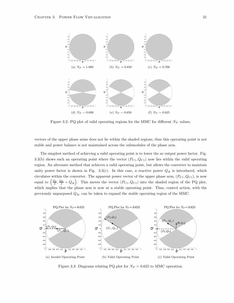
in Fig. 3.2. The shaded regions of the PQ plots indicate the stable operating regions of the converter.
Notice that for NF values ranging from 1.000 down to 0.700, power balance is met for all operating
points of the MMC. For NF values below 0.700, the figures show MMC operation cannot be maintained
for all operating points. However, control action can be taken to enable continued MMC operation below
NF values of 0.700.
Consider Fig. 3.3(a) where a single phase MMC outputs (PΣ, QΣ) = (−1.0pu, 0pu) to the grid and
NF = 0.625. The upper and lower phase arms share the output power equally. Therefore the apparent
power vector of the upper phase arm, shown as (PU1, QU1), is equal to(
PΣ
2 , QΣ
2
). The apparent power
1A Matlab script was used to perform the calculations. The details and assumptions of the Matlab script are not givenhere, but instead provided in Appendix A.2.
2The overhead voltage,κ, is equal to VDC
2VS, which is found by solving VDC = κ(2VS) for κ. The nominal modulation
index is therefore given as 1κ. In this work, κ = 1.15 and |VS | = |VΣ| = 1.0pu
(i.e.|VΣ| =
√2pu
).
Chapter 3. Power Flow Visualization 31
(a) NF = 1.000 (b) NF = 0.850 (c) NF = 0.700
(d) NF = 0.690 (e) NF = 0.650 (f) NF = 0.625
Figure 3.2: PQ plot of valid operating regions for the MMC for different NF values.
vectors of the upper phase arms does not lie within the shaded regions, thus this operating point is not
stable and power balance is not maintained across the submodules of the phase arm.
The simplest method of achieving a valid operating point is to lower the ac output power factor. Fig.
3.3(b) shows such an operating point where the vector (PU1, QU1) now lies within the valid operating
region. An alternate method that achieves a valid operating point, but allows the converter to maintain
unity power factor is shown in Fig. 3.3(c). In this case, a reactive power QΔ is introduced, which
circulates within the converter. The apparent power vector of the upper phase arm, (PU1, QU1), is now
equal to(
PΣ
2 , QΣ
2 +QΔ
). This moves the vector (PU1, QU1) into the shaded region of the PQ plot,
which implies that the phase arm is now at a stable operating point. Thus, control action, with the
previously unpurposed QΔ, can be taken to expand the stable operating region of the MMC.
(a) Invalid Operating Point (b) Valid Operating Point (c) Valid Operating Point
Figure 3.3: Diagrams relating PQ plot for NF = 0.625 to MMC operation.
Chapter 3. Power Flow Visualization 32
3.3 Complete Power Flow Visualization
The complete visualization of the MMC with distributed BES is achieved by overlaying the inter-arm
phasor diagrams atop the PQ plots generated by the intra-arm power balance test. As each individual
phase arm is independent, six graphs, each representing a single phase arm, are required to display the
power flow of the MMC.
An interactive UI tool has been developed to help visualize the power flow of the MMC with dis-
tributed BES. This section uses images generated from the UI tool, but does not cover the operation
of the tool. Instead, a full description and manual for the UI tool can be found in Appendix B. The
following images are meant as a brief introduction to the information contained in the UI tool’s figures.
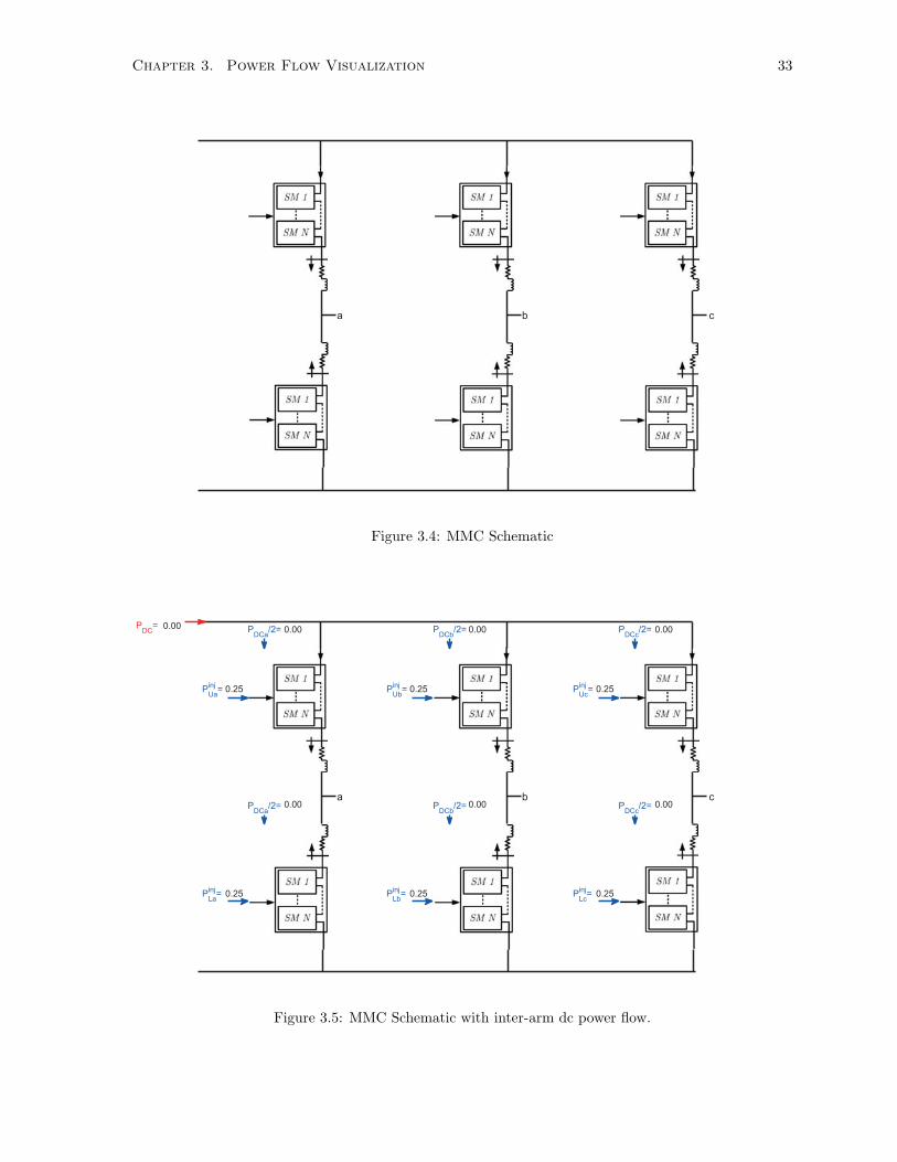
The UI tool first begins with a schematic of a three-phase MMC (Fig. 3.4) then dc and/or fundamen-
tal frequency ac power can be displayed on the schematic. The power flow has been normalized to the
phase. Thus, each phase is rated at 1.0pu and the three-phase MMC is able to output a total of 3.0pu.
To show dc power information, the dc power is labelled onto the schematic in Fig. 3.5. For each phase
arm, the power injected into the phase arm by energy storage is given by P injUx and P inj
Lx for x in {a, b, c}.If energy storage is disabled in a phase arm, the label is coloured red. Additionally, dc power transferred
into a phase arm by the dc difference current is labelled as PDCx
2 for x in {a, b, c}. The dc labels indicatethe amount of power that must be transferred out of the phase arm via fundamental frequency power.
For example, an upper phase arm of phase a must transfer P injUa + PDC
2 out of the phase arm. The PDC
label represents power transferred into the MMC from the dc link. For this discussion, the MMC with
distributed BES operates in standalone mode, thus PDC is considered zero and is coloured red.
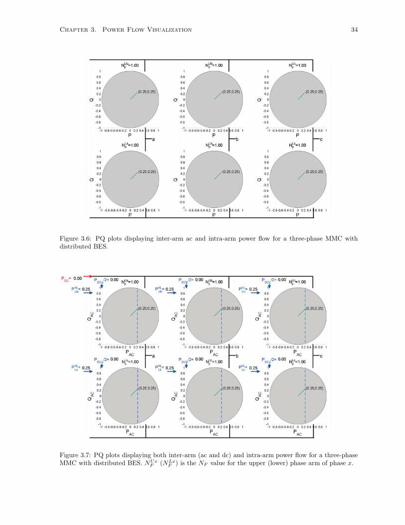
To show ac power information and intra-arm power balance results, PQ plots replace the phase arm
schematics. This is shown in Fig. 3.6 where the dc information has been removed and the PQ plots
are displayed. In the PQ plot, the intra-arm power balance test results are displayed with a phasor
representing the fundamental frequency power of the phase arm. These plots are identical to those
discussed in Section 3.2 and their associated NF value is labelled in the title. NUxF (NLx
F ) is the NF
value for the upper (lower) phase arm of phase x.
Finally, both the ac and dc power information is displayed in Fig. 3.7. As required, the fundamental
frequency power out of each phase arm equates to the dc power into each phase arm. Similar to the
phasor diagrams of Section 3.1, the tip of the fundamental frequency phasors must lie upon the blue line
to maintain power balance.
Chapter 3. Power Flow Visualization 33
a b c
Figure 3.4: MMC Schematic
0.00 0.00 0.00 0.00
0.00 0.00 0.00
0.25 0.25 0.25
0.25 0.25 0.25
a b c
PDC= PDCa/2= PDCb/2= PDCc/2=
PDCa/2= PDCb/2= PDCc/2=
PinjUa= PinjUb= PinjUc=
PinjLa= PinjLb= PinjLc=
Figure 3.5: MMC Schematic with inter-arm dc power flow.
Chapter 3. Power Flow Visualization 34
Figure 3.6: PQ plots displaying inter-arm ac and intra-arm power flow for a three-phase MMC withdistributed BES.
Figure 3.7: PQ plots displaying both inter-arm (ac and dc) and intra-arm power flow for a three-phaseMMC with distributed BES. NUx
F (NLxF ) is the NF value for the upper (lower) phase arm of phase x.
Chapter 3. Power Flow Visualization 35
3.4 Case Studies
Using the UI Tool, several power flow cases are examined for the MMC with distributed BES. These cases
are meant to describe the operation of the three-phase converter and convey an intuitive understanding
of the converter.
3.4.1 MMC with Distributed Battery Energy Storage
The case studies begin with a basic case where energy storage is installed in all the submodules of the
MMC (i.e. NF = 1.0 for all phase arms). Fig. 3.8 shows the MMC operating with (PΣx, QΣx) =
(1.0pu, 0.0pu) for each phase x. Energy storage in each phase arm provides the required 0.50pu real
power.
Suppose that 0.25pu real power is to be transferred from the upper phase arm to the lower phase
arm of phase a, Fig. 3.9 shows the resulting power flow. The real power provided by the energy storage
in phase a has changed (see P injUa and P inj
La values), while the real power output of all other phase arms
remain constant. The fundamental frequency complex power of phase b and c has instead begun to
circulate reactive power. As the reactive power sums to zero, this reactive power is not seen by the ac
grid. For the case shown, the energy storage provides all the necessary output power per phase (i.e.
P injUx + P inj
Lx = PΣx). As power balance is met for each phase, power does not need to be transferred
between phases (i.e. PDCx = 0).
Figure 3.8: MMC with distributed BES with energy storage in each phase arm outputting equal power.
Chapter 3. Power Flow Visualization 36
Figure 3.9: In this case, the energy storage in phases b and c output equal power. The energy storage inthe upper phase a phase arm is transferring power to the lower phase arm without affecting the powertransfer of the other phases.
Chapter 3. Power Flow Visualization 37
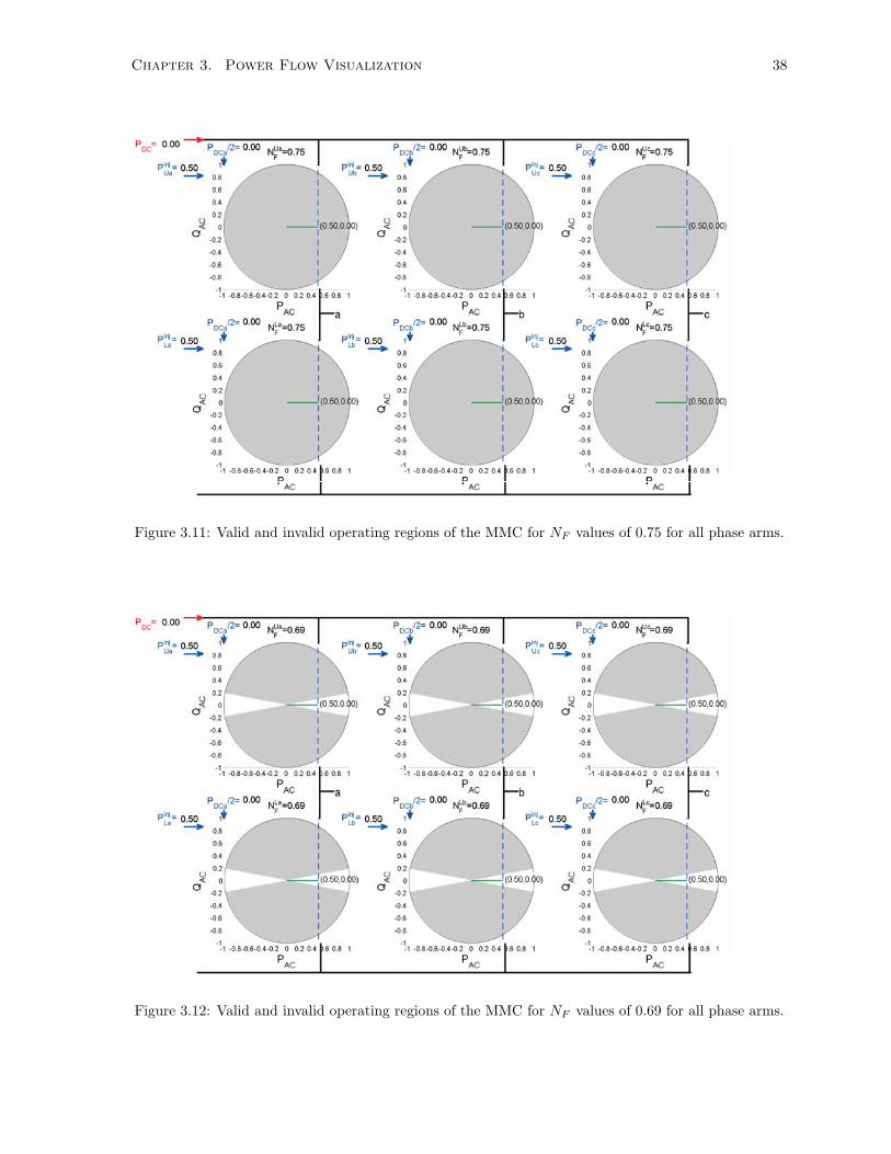
For a MMC with distributed BES in less than 100% of submodules is analyzed next. The intra-arm
power balance test was used to generate PQ plots for this configuration. From Section 3.2, it was found
that a phase arm can operate normally with NF values ranging from 1.0 to 0.70. This result does not
change for a three-phase MMC. Fig. 3.10 to 3.12 shows the power flow of a three-phase MMC for NF
values of 1.00, 0.75, and 0.69 for all phase arms. The MMC is shown to operate normally at NF values
of 1.00 and 0.75, but it can no longer operate at unity power factor for the NF value of 0.69, which is
below the 0.70 threshold. Furthermore, the intra-arm power balance results are independent for each
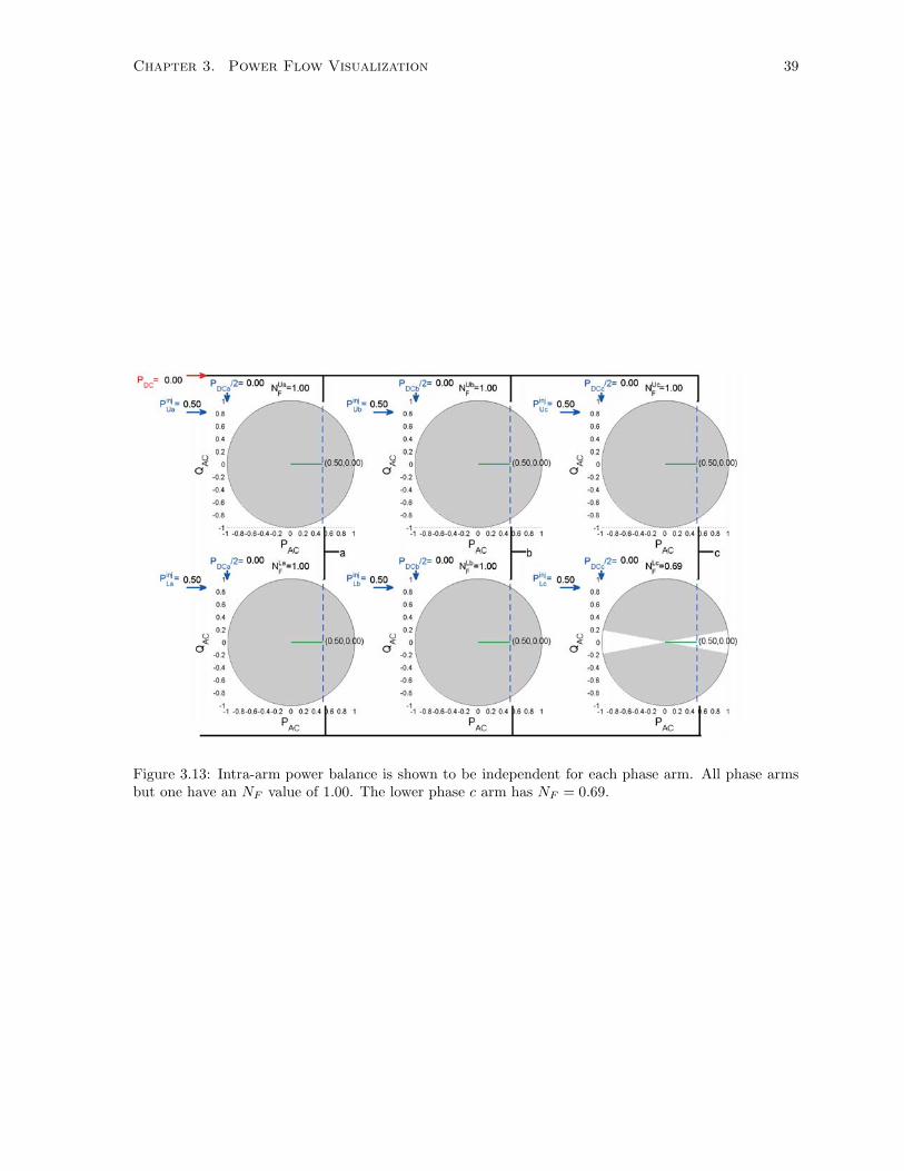
phase arm, thus each PQ plot is also independent. This is shown in Fig. 3.13 where the NF value of the
lower phase arm of phase c drops below the NF threshold of 0.69 while all other phase arms maintain a
NF value of 1.00.
This case study serves to visualize the inter-arm power flow analysis from the previous section, and
extend the intra-arm power flow results to a three-phase system. The main implication is that the MMC
can be populated with energy storage in 70% of submodules without adversely affecting operation.
Alternatively, up to 30% of battery units can be lost in an individual phase arm while still maintaining
MMC operation.
Figure 3.10: Valid and invalid operating regions of the MMC for NF values of 1.00 for all phase arms.
Chapter 3. Power Flow Visualization 38
Figure 3.11: Valid and invalid operating regions of the MMC for NF values of 0.75 for all phase arms.
Figure 3.12: Valid and invalid operating regions of the MMC for NF values of 0.69 for all phase arms.
Chapter 3. Power Flow Visualization 39
Figure 3.13: Intra-arm power balance is shown to be independent for each phase arm. All phase armsbut one have an NF value of 1.00. The lower phase c arm has NF = 0.69.
Chapter 3. Power Flow Visualization 40
3.4.2 Alternate Battery Distributions
The MMC with distributed BES can have various battery distribution configurations where three main
variants exist. These variants differ in the number phase arms with energy storage. In the first variant,
all lower (or upper) phase arms have energy storage. In the second variant, the upper and lower phase
arms of a single phase have energy storage. In the third variant, the upper and lower phase arms of two
phases have energy storage.
Variant 1 - Energy Storage in Lower Arms
For the first variant, all lower phase arms contain energy storage. Fig. 3.14 shows the power flow
when the converter outputs (PΣx, QΣx) = (1.0pu, 0.0pu) for a given phase x. As all real power must be
provided by the energy storage, the lower phase arms must carry rated output power. If necessary, the
upper phase arms could be omitted, but the converter would lose the capability to interface with a dc
network and perform inter-arm power transfer.
In terms of intra-arm power balance, the fraction of submodules with energy storage can drop from
a NF value of 1.00 to 0.70 in each phase arm without affecting operation. This is shown in Fig. 3.15,
where NF values of the phase arms are set to 1.00, 0.75, and 0.69 for phases a, b, and c, respectively.
Figure 3.14: Variant 1 is displayed where energy storage is only integrated into the lower phase arms.
Chapter 3. Power Flow Visualization 41
Figure 3.15: Variant 1 with different NF values.
Chapter 3. Power Flow Visualization 42
Variant 2 - Energy Storage in One Phase
In the second variant, only the upper and lower phase arms of phase c contain energy storage. Any phase
could be chosen, but phase c is used as an example. Fig. 3.16 shows the power flow when the converter
outputs (PΣx, QΣx) = (1.0pu, 0.0pu) for each phase x. As all real power must be provided by the energy
storage, power must be transferred from phase c to phases a and b via dc difference currents. The dc
difference current of phase c provides power to phases a and b, thus the phase c dc difference current is
twice that of the other phases. In effect, phase legs a and b would operate in the same manner as phase
legs of a standard MMC. This variant may simplify installation by centralizing all energy storage into a
single phase leg of the MMC. However, the phase leg would experience higher current stresses compared
to the other phase legs.
For this variant of the MMC with distributed BES, a dc difference current is required. This changes
the phase arm currents, which affects intra-arm power balance and alters the NF threshold from the
previous case studies. From the UI tool, operation of the converter is found to be maintained for NF
values of 1.00 to 0.94. This is shown in Fig. 3.17, where NF values are equal to 0.94 and 0.91. In the
case where NF is equal to 0.91, the power vector does not lie within the achievable operating range.
Even under reduced power transfer, the NF threshold will remain the same, as seen in Fig. 3.18 when
(PΣx, QΣx) = (0.5pu, 0.0pu).
Figure 3.16: Variant 2 is displayed where energy storage is only integrated into a single phase.
Chapter 3. Power Flow Visualization 43
Figure 3.17: Variant 2 with different NF values and (PΣ, QΣ) = (1.0pu, 0.0pu).
Figure 3.18: Variant 2 with different NF values and (PΣ, QΣ) = (0.5pu, 0.0pu).
Chapter 3. Power Flow Visualization 44
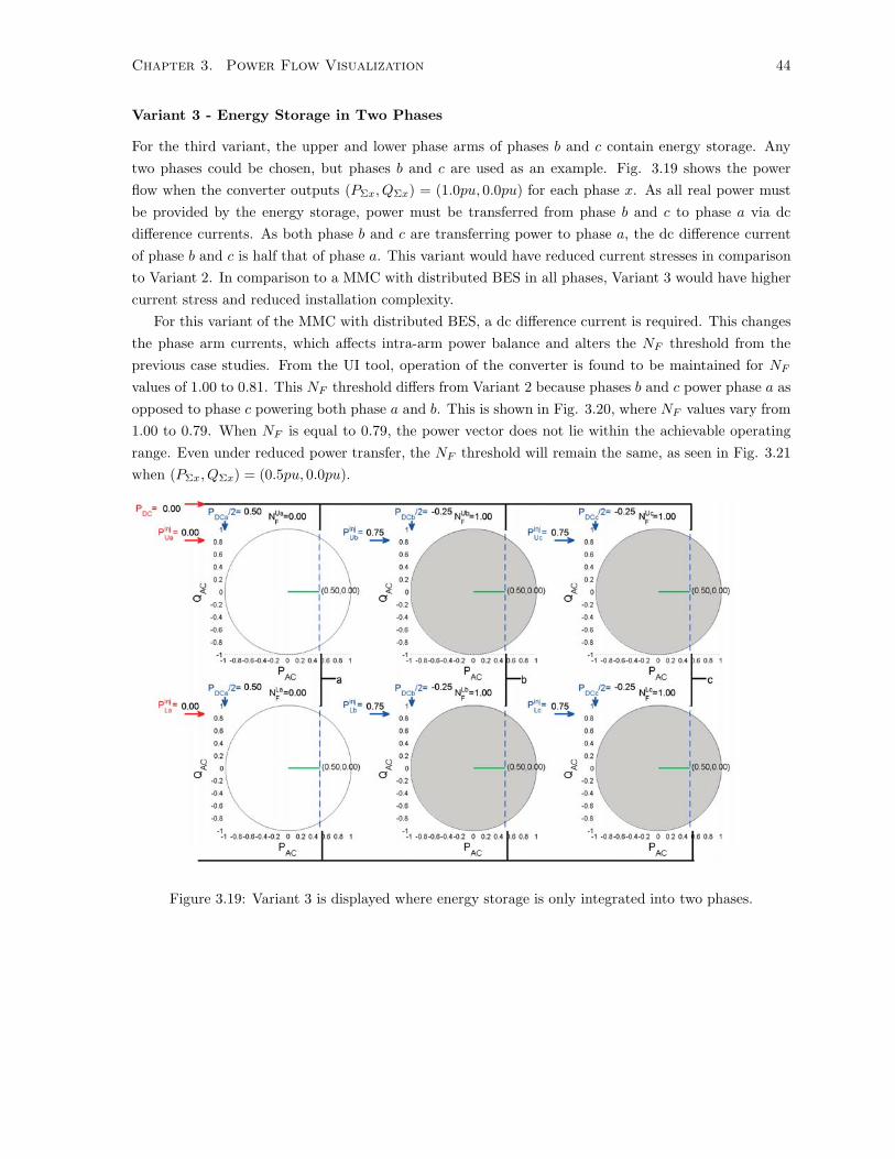
Variant 3 - Energy Storage in Two Phases
For the third variant, the upper and lower phase arms of phases b and c contain energy storage. Any
two phases could be chosen, but phases b and c are used as an example. Fig. 3.19 shows the power
flow when the converter outputs (PΣx, QΣx) = (1.0pu, 0.0pu) for each phase x. As all real power must
be provided by the energy storage, power must be transferred from phase b and c to phase a via dc
difference currents. As both phase b and c are transferring power to phase a, the dc difference current
of phase b and c is half that of phase a. This variant would have reduced current stresses in comparison
to Variant 2. In comparison to a MMC with distributed BES in all phases, Variant 3 would have higher
current stress and reduced installation complexity.
For this variant of the MMC with distributed BES, a dc difference current is required. This changes
the phase arm currents, which affects intra-arm power balance and alters the NF threshold from the
previous case studies. From the UI tool, operation of the converter is found to be maintained for NF
values of 1.00 to 0.81. This NF threshold differs from Variant 2 because phases b and c power phase a as
opposed to phase c powering both phase a and b. This is shown in Fig. 3.20, where NF values vary from
1.00 to 0.79. When NF is equal to 0.79, the power vector does not lie within the achievable operating
range. Even under reduced power transfer, the NF threshold will remain the same, as seen in Fig. 3.21
when (PΣx, QΣx) = (0.5pu, 0.0pu).
Figure 3.19: Variant 3 is displayed where energy storage is only integrated into two phases.
Chapter 3. Power Flow Visualization 45
Figure 3.20: Variant 3 with different NF values and (PΣ, QΣ) = (1.0pu, 0.0pu).
Figure 3.21: Variant 3 with different NF values and (PΣ, QΣ) = (0.5pu, 0.0pu).
Chapter 3. Power Flow Visualization 46
3.5 Summary
This chapter introduced visual tools to understand both the inter-arm and intra-arm power flow. Notably,
from the intra-arm power balance visualization, it was found that a previously unpurposed reactive
difference power (QΔ) can be used to expand the stable operating region of the MMC. In addition, the
visual tools helped identify several variants of the MMC with distributed BES. These variants all reduce
the number of submodules with energy storage within the MMC, which may simplify installation. In
addition, the visual tool demonstrates the MMC’s flexibility to operate with large steady state power
transfers within the converter. This introduces the possibility of integrating energy storage sources with
differing characteristics, such as battery and supercapacitor energy storage.
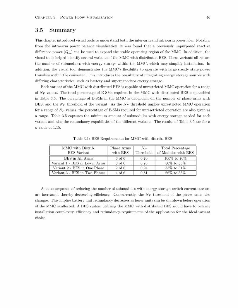
Each variant of the MMC with distributed BES is capable of unrestricted MMC operation for a range
of NF values. The total percentage of E-SMs required in the MMC with distributed BES is quantified
in Table 3.5. The percentage of E-SMs in the MMC is dependent on the number of phase arms with
BES, and the NF threshold of the variant. As the NF threshold implies unrestricted MMC operation
for a range of NF values, the percentage of E-SMs required for unresetricted operation are also given as
a range. Table 3.5 captures the minimum amount of submodules with energy storage needed for each
variant and also the redundancy capabilities of the different variants. The results of Table 3.5 are for a
κ value of 1.15.
Table 3.1: BES Requirements for MMC with distrib. BES
MMC with Distrib. Phase Arms NF Total PercentageBES Variant with BES Threshold of Modules with BES
BES in All Arms 6 of 6 0.70 100% to 70%Variant 1 - BES in Lower Arms 3 of 6 0.70 50% to 35%Variant 2 - BES in One Phase 2 of 6 0.94 33% to 31%Variant 3 - BES in Two Phases 4 of 6 0.81 66% to 53%
As a consequence of reducing the number of submodules with energy storage, switch current stresses
are increased, thereby decreasing efficiency. Concurrently, the NF threshold of the phase arms also
changes. This implies battery unit redundancy decreases as fewer units can be shutdown before operation
of the MMC is affected. A BES system utilizing the MMC with distributed BES would have to balance
installation complexity, efficiency and redundancy requirements of the application for the ideal variant
choice.
Chapter 4
Control of MMCs with distributed
BES
In this chapter, the control system for a three-phase MMC with distributed BES is developed based on
the discussions of Chapter 2 and 3. The developed controller is able to achieve independent inter-arm
power transfer between any phase arm of the MMC, and is also able to avoid the unstable operating
regions found from the intra-arm power balance analysis.
To maximize efficiency, reactive fundamental frequency difference current is minimized and the
controller also removes any undesired harmonic difference currents. Undesired harmonics also include
those that result from steady state fundamental difference currents used in MMCs with distributed BES,
which are not present in standard MMCs.
An overview of the control structure used for the MMC with distributed BES is presented in Fig. 4.1.
As feedback signal requirements of the MMC are extensive, the control structure of Fig. 4.1 separates the
control of the MMC from the BES units. This minimizes the number of signals, if any, that are passed
between the MMC and BES units. The SOC balancing of the batteries can be achieved independently
from MMC control because the SOC balancing is reflected upon the submodule capacitor voltages. As
the purpose of the MMC’s controller is to maintain submodule capacitor voltage balance, the MMC
controller does not require additional information from the BES units.
The details of the control blocks are elaborated in three sections. The discussion first focuses on the
current controllers of the MMC control structure, followed by an explanation of the difference current
reference generator block used in MMC control. Finally, this chapter concludes by describing the BES
control structure.
4.1 MMC Grid and Difference Current Control Structure
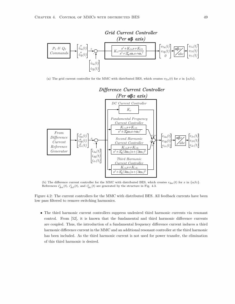
The grid and difference current controllers employed for the MMC are shown in Fig. 4.2. These
controllers are akin to [54] and [55] where a series of resonant controllers are used for each harmonic
that requires regulation. Resonant controllers are used due to their ability to track both positive and
negative sequence current components [56]. In comparison to the balancing methods in [44] and [53],
which control the amplitude of the fundamental frequency difference current, the resonant controllers
allow for control of both amplitude and phase.
47
Chapter 4. Control of MMCs with distributed BES 48
+
-
Three-Phase MMC
-
VDC2
VDC
VDC
+
+
VDC2
Sort
Sort
-
v a(t)v b(t)v c(t)
v a(t)v b(t)v c(t)
Grid Current Controller
Difference Current Controller
Difference Current Reference Generator
Output Power Commands
PUa PUb PUc
PLa PLb PLc
*inj *inj *inj
*inj *inj *inj(Optional, Requested Power from BES)
Per E-SM
Per Upper (Lower) Arm of Phase x
PUa PUb PUc
PLa PLb PLc
*inj *inj *inj
*inj *inj *inj
BES Power Commands
BES Controller BIC
SM Capacitor Voltage Setpoints
Intra-ArmSOC
Balancer
Inter-ArmSOC
Balancer
Total Requested
Power from the
BES units
Figure 4.1: Overview of the control structure used for the MMC with distributed BES.
The grid current controller is shown in Fig. 4.2(a). It regulates the grid currents in the α and β
frame to achieve the desired real and reactive power transferred to the grid (i.e. PS and QS). The zero
sequence axis is not regulated, as there is no path for the zero sequence current to flow.
The difference current controller is shown in Fig. 4.2(b). It regulates the difference current in the
αβz1 frame to maintain capacitor voltage balance (i.e. power balance) in all submodules. Each αβz
axis controller of Fig. 4.2(b) consists of four current controllers that control the 1) dc, 2) fundamental
frequency, 3) second harmonic, and 4) third harmonic components of iΔ(t). The function of each current
controller is summarized as follows:
• The dc current controllers in the αβz reference frame assign the power PDCx to each phase via
proportional control. A proportional-integral (PI) controller is not used, since the current reference
generator contains a PI controller. A proportional term in the current controller avoids the use of
two integral controllers in series to avoid stability issues.
• The fundamental frequency current controllers in the αβz reference frame assign the real and
reactive power transfer between upper and lower phase arms (i.e. PΔx and QΔx) via resonant
control.
• The second harmonic current controllers suppress undesired second harmonic currents to minimize
arm conduction loss via resonant control.
1The zero sequence component is identified by “z”.
Chapter 4. Control of MMCs with distributed BES 49
KGs2+KGas+KGb
s2+2 G ss+ s2
PS & QS
Commandsv (t)v (t)
0
zabc
v a(t)v b(t)v c(t)
*
*i (t)i (t)
i (t)i (t)
-+
(a) The grid current controller for the MMC with distributed BES, which creates vΣx(t) for x in {αβz}.
Fundamental Frequency Current Controller
++
Second Harmonic Current Controller
+
Third Harmonic Current Controller
DC Current Controller
+
Kp
s2+2 (3 S)s+(3 S)2Kr3as+Kr3b
s2+2 (2 S)s+(2 S)2Kr2as+Kr2b
s2+2 Ss+ S2
Kr1as+Kr1b
i (t)i (t)i z(t)
***
i (t)i (t)i z(t)
v (t)v (t)v z(t)
zabc
v a(t)v b(t)v c(t)-
+From
Difference Current
Reference Generator
(b) The difference current controller for the MMC with distributed BES, which creates vΔx(t) for x in {αβz}.References i∗Δα(t), i
∗Δβ(t), and i∗Δz(t) are generated by the structure in Fig. 4.3.
Figure 4.2: The current controllers for the MMC with distributed BES. All feedback currents have beenlow pass filtered to remove switching harmonics.
• The third harmonic current controllers suppress undesired third harmonic currents via resonant
control. From [52], it is known that the fundamental and third harmonic difference currents
are coupled. Thus, the introduction of a fundamental frequency difference current induces a third
harmonic difference current in the MMC and an additional resonant controller at the third harmonic
has been included. As the third harmonic current is not used for power transfer, the elimination
of this third harmonic is desired.
Chapter 4. Control of MMCs with distributed BES 50
4.2 Generation of Difference Current References
From the discussion in Chapter 2, it was found that the dc power, PDCx, and average difference power,
PΔx, as indicated in Fig. 2.4, for a given phase x can be independently controlled for each phase.
The power PDCx is controlled with the dc difference current IΔ0x and PΔx is controlled with positive
and negative sequence fundamental frequency difference current iΔ1x(t). To avoid the unstable regions
presented by the intra-arm power balance analysis, positive sequence reactive fundamental frequency
difference current is employed.
The process for generating the difference current references to maintain power balance across all
phase arms is depicted in Fig. 4.3. From the figure, reference generation is divided into dc difference
currents and fundamental frequency difference currents reference generators.
4.2.1 DC Difference Current
The dc difference current reference generator of Fig. 4.3 regulates the mean sum of the total submodule
capacitor voltage of the upper and lower phase arms, denoted as vCUx(t) and vCLx(t) for a given phase
x. If the mean sum deviates from its nominal value, it implies that there is a power imbalance between
different phases of the converter. Thus, the mean sum is used to regulate PDCx for a given phase x by
creating a IΔ0x current reference via PI control. The individual phase references are converted into the
αβz reference frame for use by the current controllers. The dc difference current in the α and β axes
manipulates the dc power transfer between the phase legs. The z axis current, IΔ0z , gives the dc current
flowing from the external dc grid.
4.2.2 Fundamental Frequency Difference Current
The fundamental frequency difference current reference generator of Fig. 4.3 creates current references,
i∗Δ1α(t), i∗Δ1β(t), and i∗Δ1z(t), to equalize upper and lower arm submodule capacitor voltages, while min-
imizing circulating reactive current. From Section 2.2, the analysis showed that the average powers
PΔa, PΔb, PΔc, and∑
QΔ are independently controllable. Thus, power could be independently trans-
ferred between the upper and lower phase arms in each phase of the MMC. To create the average power
references, P ∗Δa, P
∗Δb, P
∗Δc, and
∑Q∗
Δ, two different processes are used.
Generation of P ∗Δa, P
∗Δb, and P ∗
Δc
The first process generates PΔa, PΔb, and PΔc reference values by using vCUx(t) and vCLx(t) for a given
phase x as feedback. A mean difference between vCUx(t) and vCLx(t) of phase x implies an imbalance in
power between the phase arms. Thus, the mean difference is used to create a PΔx reference for a given
phase x via PI control. Given the knowledge of P inj∗Ux and P inj∗
Lx , a feedforward term,(
P inj∗Ux −P inj∗
Lx
2
),
may be added to improve response time.
Generation of∑
Q∗Δ
The second process generates a∑
QΔ reference value. From Section 3.2, it was found that intra-arm
power balance could be maintained below the NF threshold by either decreasing the output power factor
on the ac terminals of the converter or by circulating a reactive difference current within the converter.
The latter option would be controlled by manipulating QΔ reference value. As QΔ referred to the single
Chapter 4. Control of MMCs with distributed BES 51
-+
vCLx(t)
vCUx(t) x
PUx - PLx
++
2 V
inj*
vCUx(t) + vCLx(t)-2VDC
+*
H(s)
Per Phase x
Per Phase x
++ i (t)
i (t)i z(t)
3 0abc
H(s)
3
I 0x
Fundamental Frequency Difference Current Reference Generator
DC Difference Current Reference Generator
I 0
I 0
I 0z
i 1 (t)i 1 (t)
0
*
*
*
*
*
*
*
*
inj*sKp+ Ki
sKp+ Ki
*
*
Figure 4.3: Reference creation for difference current controllers. The voltages vCUx(t) and vCLx(t)denote the sum of all submodule capacitor voltages in the upper or lower arm of a given phase x. H(s)is a low pass filter.
phase reactive difference power, the three phase reactive difference power equivalents are QΔa, QΔb,
and QΔc. However, the inter-arm power balance scheme restricts the reactive power control variables
to∑
QΔ only. Thus,∑
QΔ is used to manipulate the circulating reactive difference current within
the converter 2. If intra-arm power balance were to be achieved by adjusting the output power factor,
the operating range of the MMC would be limited, which may not be desired. Alternatively, most
applications do not use∑
QΔ as it only circulates within the converter, thus it is generally set to zero.
Therefore, the previously unpurposed∑
QΔ is an appealing candidate for regulation of intra-arm power
balance.
Two methods can be used to determine the reference value of∑
QΔ, which are shown in Fig. 4.4.
The first method is to use the developed Matlab graphical tool to generate a look up table of∑
QΔ
values. Based on the NF values of the phase arms and the operating point of the MMC, the value
of∑
QΔ would be pre-determined. The second method would regulate the intra-arm power balance
dynamically by using the difference between capacitor voltages.
From experimental results, the submodule capacitor voltage of the E-SMs would diverge from the S-
SMs (E-SMs with their BES units shutdown effectively become S-SMs). When the submodule capacitor
voltages diverge, the capacitor voltage of the E-SMs diverge together likewise with the S-SMs. If the
voltage difference between the E-SMs and S-SMs is not too large, the submodule capacitor voltages
settle to steady state values. Thus, the voltage difference can be used as feedback to control∑
QΔ to
maintain intra-arm power balance. The feedback relies on a single feedback signal denoted by Σ|vcδ(t)|
2∑
QΔ causes balanced, positive sequence reactive difference power to circulate within the MMC. Balanced negativesequence QΔ is employed for inter-arm power balance and zero sequence QΔ is removed via control.
Chapter 4. Control of MMCs with distributed BES 52
*
*+
++
- +-C
bl*sKi
Kp
Figure 4.4: Possible∑
QΔ reference generation blocks.
and is defined as:
Σ|vcδ(t)| = ΣNm=1
∣∣∣∣vmCUa(t)−vCUa(t)
N
∣∣∣∣+ΣNm=1
∣∣∣∣vmCUb(t)−vCUb(t)
N
∣∣∣∣+ . . .
+ΣNm=1
∣∣∣∣vmCLc(t)−vCLc(t)
N
∣∣∣∣(4.1)
where vmCUx(t) is the mth submodule capacitor voltage of phase arm Ux for a given phase x and vmCLx(t)
is similarly the mth submodule capacitor voltage of phase arm Lx for a given phase x. When Σ|vcδ(t)|is non-zero, it implies that the E-SM and S-SM sumbodule capacitor voltages are diverging from each
other and intra-arm power balance is not maintained. Thus,∑ |vCδ(t)| is used to create
∑QΔ reference
value via PI control. However, a modification must be made to the PI controller as∑ |vCδ(t)| is an
absolute value, which would cause the integral term of the PI controller to either increase or be static.
An offset is introduced to the feedback signal path by subtracting the offset V ∗bl from
∑ |vCδ(t)|. This
introduces a small steady state error, but prevents integral wind-up of the∑
QΔ reference value. A
lower limit of zero has also been placed on∑
QΔ reference value.
Completing the Fundamental Frequency Reference
Once PΔa, PΔb, PΔc, and∑
QΔ references have been generated, the analysis from Section 2.2 showed
that these variables could be mapped to positive and negative sequence components in the fundamental
frequency difference currents. To simplify computation, the positive and negative sequence components
are determined by choosing the following four independent variables: 1) I(p)Δ1cos(γ
(p)), 2) I(p)Δ1sin(γ
(p)), 3)
I(n)Δ1 cos(γ
(n)), and 4) I(n)Δ1 sin(γ
(n)). For control, the variables are mapped onto a fundamental frequency
space vector:
iΔ1α(t) + jiΔ1β(t) =[I(p)Δ1cos(γ
(p)) + jI(p)Δ1sin(γ
(p))]ejθΣ(t)
+[I(n)Δ1 cos(γ
(n))− jI(n)Δ1 sin(γ
(n))]e−jθΣ(t)
(4.2)
Chapter 4. Control of MMCs with distributed BES 53
where θΣ(t) is the angle of vΣα(t) + jvΣβ(t).
The mapping process is shown in Fig. 4.3 by converting the reference power commands P ∗Δa, P
∗Δb,
P ∗Δc, and
∑Q∗
Δ to the fundamental frequency difference current references, i∗Δ1α(t) and i∗Δ1β(t), using
(2.11) and (4.2) to the αβz frame.
The difference current reference is completed by summing the dc and fundamental frequency differ-
ence current references in the αβz reference frame.
4.3 Control of Power Injection by BES
The developed MMC controller is solely dependent on the submodule capacitor voltages, which implies
that minimal communication is required between the MMC controller and BES controllers. The only
external input required to the BES controller is the total requested power from all BES units, PES,TOT .
If the SOC of all BES units were equal then each BES unit would deliver an equal amount of power,
otherwise an energy balancing algorithm must be employed. Energy balance between BES units can
be co-ordinated in similar categories as the inter-arm and intra-arm power balance of the MMC. Thus,
energy balancing of BES units between different phase arms is referred to as inter-arm SOC balancing
and energy balancing of BES units within an individual phase arm is referred to as intra-arm SOC
balancing.
At the inter-arm level, each BES unit would ideally deliver an equal amount of power. Thus, the
requested power from each phase arm is
P inj∗Ux = P ∗
ES,TOT
(NES,Ux∑
NES
)(4.3a)
P inj∗Lx = P ∗
ES,TOT
(NES,Lx∑
NES
)(4.3b)
for x ∈ {a, b, c}. The symbol∑
NES denotes the total number of E-SMs in the MMC, and NES,Ux and
NES,Lx denote the number of E-SMs in the upper and lower phase arm, respectively.
The inter-arm SOC balancer would be required if the SOC between phase arms were to drift. It
regulates the average SOC of each phase arm by adjusting the BES power commands of each phase
arm(i.e. P inj∗
Ux and P inj∗Lx for x in {a, b, c}
)to achieve balance. When the BES units are discharging(
i.e. P ∗ES,TOT ≥ 0
), the following commands are issued
P inj∗Ux = P ∗
ES,TOT
(NES,Ux∑
NES
)(SOCAV G
Ux
SOCAV GTOT
)if P ∗
ES,TOT ≥ 0 (4.4a)
P inj∗Lx = P ∗
ES,TOT
(NES,Lx∑
NES
)(SOCAV G
Lx
SOCAV GTOT
)if P ∗
ES,TOT ≥ 0 (4.4b)
where SOCAV GUx and SOCAV G
Lx are the average SOC of the BES units in the upper and lower arm, and
SOCAV GTOT is the average SOC of all BES units in the MMC with distributed BES. These commands
ensure that BES units with lower SOC deliver less power than the other BES units to eventually balance
the SOC of all units. By scaling references using SOCAV GUx and SOCAV G
Lx relative to SOCAV GTOT , the total
injected power sums to the desired PES,TOT ∗. This can be shown by summing P inj∗Ux and P inj∗
Lx across
Chapter 4. Control of MMCs with distributed BES 54
all phases as follows
∑x∈{a,b,c}
(P inj∗Ux + P inj∗
Lx
)= P ∗
ES,TOT
∑x∈{a,b,c}
[(NES,Ux∑
NES
)(SOCAV G
Ux
SOCAV GTOT
)+
(NES,Lx∑
NES
)(SOCAV G
Lx
SOCAV GTOT
)](4.5)
where
SOCAV GUx =
NES,Ux∑k=1
SOCkUx
NES,Ux(4.6)
SOCAV GLx =
NES,Lx∑k=1
SOCkLx
NES,Lx(4.7)
SOCAV GTOT =
1∑x={a,b,c} (NES,Ux +NES,Lx)
∑x={a,b,c}
⎛⎝NES,Lx∑
k=1
SOCkLx +
NES,Ux∑k=1
SOCkUx
⎞⎠ . (4.8)
where SOCkUx and SOCk
Lx are the state of charge of the BES unit in the kth E-SM of the phase arm.
Substituting (4.6) to (4.8) into (4.5) results in
∑x∈{a,b,c}
(P inj∗Ux + P inj∗
Lx
)= P ∗
ES,TOT
∑x∈{a,b,c}
∑NES,Ux
k=1 SOCkUx +
∑x∈{a,b,c}
∑NES,Lx
k=1 SOCkLx∑
x∈{a,b,c}(∑NES,Lx
k=1 SOCkLx +
∑NES,Ux
k=1 SOCkUx
) (4.9)
= P ∗ES,TOT (4.10)
as desired. A similar approach can applied when the BES units are charged(i.e. P ∗
ES,TOT < 0)and
would result in
P inj∗Ux = P ∗
ES,TOT
(NES,Ux∑
NES
)(2− SOCAV G
Ux
SOCAV GTOT
)if P ∗
ES,TOT < 0 (4.11a)
P inj∗Lx = P ∗
ES,TOT
(NES,Lx∑
NES
)(2− SOCAV G
Lx
SOCAV GTOT
)if P ∗
ES,TOT < 0. (4.11b)
In summary, the inter-arm SOC balancer utilizes the following equations to set the power reference
for the BES units in the upper and lower phase arms when discharging and charging the BES units:
P inj∗Ux =
⎧⎨⎩ P ∗
ES,TOT
(NES,Ux∑
NES
)(SOCAV G
Ux
SOCAV GTOT
)if P ∗
ES,TOT ≥ 0
P ∗ES,TOT
(NES,Ux∑
NES
)(2− SOCAV G
Ux
SOCAV GTOT
)if P ∗
ES,TOT < 0(4.12a)
P inj∗Lx =
⎧⎨⎩ P ∗
ES,TOT
(NES,Lx∑
NES
)(SOCAV G
Lx
SOCAV GTOT
)if P ∗
ES,TOT ≥ 0
P ∗ES,TOT
(NES,Lx∑
NES
)(2− SOCAV G
Lx
SOCAV GTOT
)if P ∗
ES,TOT < 0.. (4.12b)
These equations ensure that the total power injected by all BES units sums to P ∗ES,TOT as desired.
At the intra-arm level, each BES unit within a phase arm would ideally deliver an equal amount of
power. Thus, each BES unit in the upper arm should deliverP inj
Ux
NES,Ux, and each BES unit in the lower
arm should deliverP inj
Lx
NES,Lxwhere NES,Ux and NES,Lx are the number of E-SMs in the upper or lower
phase arm of a given phase x. The intra-arm SOC balancer would be required if the SOC between phase
Chapter 4. Control of MMCs with distributed BES 55
arms were to drift. The intra-arm SOC balancer would act upon the average SOC of each phase arm,
and would adjust the BES power commands of each BES unit to achieve balance. The following two
equations are used to adjust the BES power commands of the upper and lower phase arms:
P inj∗Ux,k =
⎧⎨⎩ P inj∗
Ux
(SOCk
Ux
SOCAV GUx
)if P inj∗
Ux ≥ 0
P inj∗Ux
(2− SOCk
Ux
SOCAV GUx
)if P inj∗
Ux < 0(4.13a)
P inj∗Lx,k =
⎧⎨⎩ P inj∗
Lx
(SOCk
Lx
SOCAV GLx
)if P inj∗
Lx ≥ 0
P inj∗Lx
(2− SOCk
Lx
SOCAV GLx
)if P inj∗
Lx < 0.(4.13b)
where k ∈ {1, · · · , NES} and denotes the kth E-SM. Equations (4.13a) and (4.13b) apply the same
strategy as (4.12a) and (4.12b) to balance the SOC between BES units within a phase arm. Once again,
(4.12a) and (4.12b) ensure that the requested power from the BES units in a phase arm total to the
requested P inj∗Ux or P inj∗
Lx . Note that each BES unit is itself a short string of battery cells, and each BES
unit would manage SOC balancing between its own battery cells.
Once a power command, either P inj,k∗Ux or P inj,k∗
Lx , is generated for each battery interface converter
(BIC), the command is realized with the control structure shown in Fig. 4.5. The BIC receives the
power command, and translates the command to a current reference based on the BES unit’s voltage.
A current controller then ensures that the desired power is delivered from the BES unit.
C
kth E-SM of Phase Arm Ux or LxBES and Chopper
-+
iES(t)VES
iES(t)(PLx ) PI VES
*PUx
inj,k*inj,k
k k
k
k
Figure 4.5: Control diagram for a BES unit in the kth E-SM of phase arm Ux or Lx for x in {a, b, c}.The current ikES(t) has been low pass filtered to remove switching harmonics.
4.4 Summary
This chapter presented the control scheme used for the MMC with distributed BES. This control scheme
allows for independent power transfer between phase arms, thus facilitating energy balance between
BES units in different phase arms of the converter. Independent power transfer is achieved through the
manipulation of the dc and fundamental difference currents, and is designed such that the difference
currents do not affect dc or ac terminals of the converter. Thus, all power transfer between BES units is
achieved internally to the MMC and the developed controls could be used to augment existing control
schemes. Of note is the use of the previously unpurposed reactive difference power,∑
QΔ, which is
now used to maintain intra-arm power balance. To determine the appropriate value of∑
QΔ, it was
suggested that a look up table could be used or a dynamic solution could utilize the submodule capacitor
voltage as feedback. These features of the proposed controller are accomplished while decoupling BES
Chapter 4. Control of MMCs with distributed BES 56
management and MMC control. This is achieved by basing MMC control on submodule capacitor
voltages, but maintaining scalability by using aggregate submodule capacitor voltages for feedback and
a sorting algorithm to manage submodule capacitor voltage balance. Table 4.4 summarizes the employed
difference current components and their utility.
Table 4.1: Effect of Difference Current Components
Difference Frame Sequence UtilityCurrent Axis
DC (IΔ0) α, β - Power transfer between phase legsDC (IΔ0) z - Controls dc link current
Fundamental α, β Positive (Real) Balanced power transfer from upperFrequency (iΔ1(t)) phase arms to lower phase arms.
Fundamental α, β Positive (Real), Power transfer from upper phase armFrequency (iΔ1(t)) Negative to lower phase arm of a single phase
(Real and Reactive) without disturbing dc link currentFundamental α, β Positive (Reactive) Shifts MMC operating point to avoid
Frequency (iΔ1(t)) unstable operating points when belowthe NF threshold
Fundamental z - Undesired, disturbs dc linkFrequency (iΔ1(t))
The structure of the MMC with distributed BES allows BES management to be distributed into
three effective levels. At the highest level, inter-arm SOC is balanced by adjusting the requested P injUx
and P injLx for x ∈ {a, b, c}. At the next level, intra-arm SOC is balanced by adjusting the requested
P inj,kUx or P inj,k
Lx between BES units within a phase arm. Finally, each BES unit would manage the SOC
between its own battery cells. In case of BES unit shutdown, the derived structure ensures the power
commands automatically scale with the number of E-SMs in each phase arm (i.e. NES,Ux or NES,Lx for
x ∈ {a, b, c}). Coupled with the developed MMC controller, the MMC would automatically adjust its
power flow to compensate for BES unit shutdown.
Chapter 5
Design of a MMC with Distributed
BES
This chapter is focused on the design and implementation of a MMC with distributed BES and is divided
into two major sections. The first section develops the design equations used in creating the converter,
and the second section details the implementation of a 600Vll,rms/100kVAMMC with 4MJ of distributed
energy storage.
5.1 MMC with Distributed BES Design
This section covers the design equations used to rate the components of MMCs with distributed BES.
The design equations in this section assume that the MMC is used as a standalone MMC with distributed
BES where all submodules are E-SMs. As the MMC with distributed BES could be used as a standard
MMC, equations for a standard MMC are also provided in Appendix F. For reference, the schematic
for the MMC is repeated in Fig. 5.1.
abc
Phase Arm Phase Leg
DC Link
+
-
SM 1
SM N
SM 1
SM N
SM 1
SM N
SM 1
SM N
SM 1
SM N
SM 1
SM N
(a) MMC Converter Structure
(b) Standard Submodule(S-SM)
(c) Energy Storage Submodule(E-SM)
Figure 5.1: The MMC with two submodule variants.
57
Chapter 5. Design of a MMC with Distributed BES 58
To define the component ratings, the following information is required: the ac grid voltage (vS(t)),
the power rating of the converter (Srated), and the overhead voltage (κ). The overhead voltage, κ,
specifies the additional voltage headroom required for control and voltage drop across grid interface
impedances(i.e. 1κ is the nominal modulation index
).
From vS(t) and κ, the dc link voltage can be immediately specified by
VDC = 2κVS . (5.1)
The power rating of the converter with the ac grid voltage would determine the rated peak value of the
ac output current, IΣ.
5.1.1 Phase Arm Inductor
The purpose of the phase arm inductor is to limit the rate of change of current during switching transi-
tions in the phase arms and faults, and to provide filtering of both ac and dc output currents.
Phase Arm Inductor Sizing
The phase arm inductor must be sized to meet the harmonic specifications of the converter. In addition,
considerations must also be made to limit the phase arm current’s rate of change during events such as
faults or a missed gate pulse. However, for this discussion, inductor sizing is based on the harmonics
only.
The inductors of a dc/ac converter are sized to limit the current harmonics produced by the converter.
When a voltage is requested by the converter’s controller, it is realized with the aid of a modulation
scheme. However, the modulation scheme would also create voltage harmonics as a by product, which
in turn induces current harmonics from the converter.
To determine the phase arm inductor’s size, the expected voltage produced by the MMC’s modulation
scheme can be generated numerically. A FFT can then be performed on the resulting voltage waveform,
and the voltage at each frequency can be divided by the phase arm inductor’s impedance. This process
can be applied to a single phase of the MMC to determine the harmonic currents produced for a given
phase arm inductor, which can be adjusted to meet specifications. Additional details with example
calculations can be found in Appendix D.
Inductor Voltage Rating
The voltage of the inductor must be rated for the line to line grid voltage in case of faults. Therefore,
Inductor Voltage Rating : VS(ll, rms). (5.2)
Inductor Current Rating
The current rating of the inductor must be at least equal to the RMS current of the phase arm, but
its saturation current must be higher than the peak current of the phase arm. The resulting RMS and
Chapter 5. Design of a MMC with Distributed BES 59
Peak current ratings would be:
Inductor RMS Current Rating :1√2
IΣ2
(5.3a)
Inductor Peak Current :IΣ2. (5.3b)
5.1.2 Submodule Capacitor
The submodule capacitor allows the MMC to safely produce a multilevel waveform. It limits the voltage
across the submodule switches and eliminates the need for a dc link capacitor [12].
Submodule Capacitor Sizing
The submodule capacitor must be sized to meet a ripple voltage specification of the converter. This
can be achieved by modelling the phase arm as a single representative submodule, and finding the
instantaneous power into the submodule capacitor. By integrating the instantaneous power to find the
instantaneous energy of the submodule, the capacitor voltage ripple can be found.
For the MMC with distributed BES, the total energy of the phase arm is:
e(t) =1
2
C
NV 2DC +
√2VDCIΣ4ω
sin(ωt+ φ)− VSIΣ4ω
cos(2ωt+ φ) (5.4)
Equation (5.4) can then be used to solve for instantaneous voltage of the capacitor, which allows the
capacitor size to be chosen to meet capacitor voltage ripple specifications. Additional details with
example calculations can be found in Appendix C.
Submodule Capacitor Voltage Rating
A MMC with N modules would produce an multilevel output voltage of N + 1 steps. To achieve this,
each submodule capacitor must be rated for a nominal voltage of
SM Capacitor Voltage Rating :VDC
N. (5.5)
Submodule Capacitor RMS Current Rating
The current rating of the submodule capacitor for a MMC with distributed BES is given by
SM Capacitor RMS Current Rating = 2
√I2Σκ2
[(1
128+
κ2
32
) −1
2+(− κ
32
) 1
π+(− κ
32
) −1
3π
](5.6)
The derivation of (5.6) is included in Appendix E.
5.1.3 Submodule Switch Rating
The submodule switches must withstand the submodule capacitor’s voltage rating and be able to conduct
the MMC’s average and peak currents.
Chapter 5. Design of a MMC with Distributed BES 60
Submodule Switch Voltage Rating
To withstand the submodule capacitor’s voltage rating, each submodule switch must be rated for a
nominal voltage of
Switch Voltage Rating :VDC
N(5.7)
Submodule Switch Current Rating
The average, RMS, and peak currents of the submodule switches in a MMC with distributed BES are
based on the current of the phase arms. These three quantities can be found with the following equations:
SM Average Current :IΣπ
(5.8a)
SM RMS Current :IΣ
2√2
(5.8b)
SM Peak Current :IΣ2
(5.8c)
where the submodule switch is rated by using the peak current of the submodule.
5.1.4 Battery Interface Converter
The battery interface converter (BIC) is a dc/dc power converter that is used to interface a BES unit
to the submodule capacitor in an E-SM. In this design, a two quadrant chopper is used as a BIC. Thus,
standard design practices, which can be found in [57], can be followed.
The purpose of the BIC is to decouple the BES unit from the submodule capacitor, and prevent
low order harmonic current from entering the BES unit. This requirement dictates the BIC’s switching
frequency as the BIC must have high enough bandwidth to eliminate the desired current harmonics
without incurring excessive switching losses losses.
The BIC also steps-up the BES unit’s voltage to the submodule capacitor’s voltage of VDC
N to decrease
the number of series connected batteries. At the same time, the BIC should be operated in a region of
high efficiency. For example in low voltage applications, a two quadrant chopper is efficient at step-up
ratios from 2-3 [58], which implies that the minimum battery voltage size is ideally 13VDC
N .
Chapter 5. Design of a MMC with Distributed BES 61
5.2 Prototype MMC with Distributed BES
This section is focused on the implementation of the MMC with distributed energy storage shown
in Fig. 5.2. The discussion is divided into four different sections, which cover 1) the design of a
600Vll,rms/100kVA MMC, 2) the design of 4MJ of supercapacitor energy storage, 3) embedded con-
trol system requirements, and 4) ancillary software algorithms for the MMC. Due to laboratory safety
concerns, the BES units have been replaced by supercapacitor energy storage units.
Figure 5.2: Picture of experimental system.
5.2.1 MMC Design
To validate the power flow analysis and control method, a prototype MMC was developed. To emulate
the characteristics of full scale MMCs, IGBT switch technology was chosen for use. To ensure that
the IGBTs were appropriately sized while maintaining a safe operating voltage within the lab, the
lowest voltage IGBT modules were chosen. Thus, 600V 200A IGBTs were used in the design of the
MMC, specifically Infineon’s BSM 200 GB 60 DLC IGBT. To utilize the IGBT’s capabilities, while still
considering faults, the MMC was rated for 600Vll,rms/100kVA and consists of four submodules per phase
arm (i.e. N = 4). The MMC’s ratings were assigned based on the voltage and current ratings of the
IGBTs. Four submodules are chosen, as it is the minimum number of submodules that would allow for
the investigation into faulted submodules. The component ratings of the prototype MMC are provided
in Table 5.1. The components do differ from the design equations for the MMC with distributed BES.
Chapter 5. Design of a MMC with Distributed BES 62
This difference is attributed to added safety margin and part availability.
Rated AC Grid Voltage (ll,rms), VS 600 VRated AC Grid Current (ll,rms), IΣ 100 ARated 3φ Power of MMC, Srated 100 kVA
Rated DC Bus Voltage, VDC (κ = 1.15) 1100 VDC Surge Voltage Rating 1400 V
Number of Modules per Arm, N 4AC Grid Frequency, fS 60HzInductor Voltage Rating 690 Vll,rms
Inductor RMS Current Rating 100 Arms
Capacitor Voltage Rating 350 VCapacitor RMS Current Rating 50 Arms
Submodule Switch Voltage Rating 600 VSubmodule Switch Average Current Rating 200 ASubmodule Switch Peak Current Rating 400 Apk
The MMC is shown in Fig. 5.3. Each phase arm of the MMC is composed of three separate layers,
which are displayed in Fig. 5.4. The first layer of the phase arm is the IGBT, submodule capacitors,
and heatsink shown in Fig. 5.4(a). The second layer of the phase arm is a printed circuit board (PCB)
that is used for the power connections, which is shown in Fig. 5.4(b). The final layer of the phase arm
contains all the logic and IGBT drivers, which is shown in Fig. 5.4(c).
A schematic diagram of the three-phase experimental system is shown in Fig. 5.5. As previously
discussed, only a fraction of submodules require BES units. Thus, all findings can be verified with
energy storage installed in only the converter’s phase c submodules. These are denoted as E-SM in the
diagram. As can be seen from the diagram, there are a total of 6 E-SMs in phase c of the MMC. All other
submodules are S-SMs. The associated single-phase configuration of the system can be seen in Fig. 5.6
where only phase c of the three-phase MMC is utilized in the single-phase arrangement. Experimental
parameters can be found in Table 5.2 and 5.3 for three-phase and single-phase experiments respectively.
For the experimental results, the MMC is derated in consideration of additional voltage stresses present
in the cases of study.
Chapter 5. Design of a MMC with Distributed BES 63
Figure 5.3: Picture of the developed three-phase MMC.
Chapter 5. Design of a MMC with Distributed BES 64
(a) Phase Arm IGBTs and Capacitors (b) Phase Arm Bus Bar PCB
(c) Phase Arm Driver Board
Figure 5.4: Pictures of the phase arm components.
Chapter 5. Design of a MMC with Distributed BES 65
Table 5.2: Three-Phase Experimental Parameters
VS 480 V AC Grid Voltage (ll,rms)VDC 880 V DC Bus Voltage
Max. VES 162 V Maximum Supercapacitor Bank VoltageSrated 83 kVA Rated 3φ Power of MMCN 3 Number of Modules per ArmfS 60 Hz AC Grid Frequency
fMMC 2.0 kHz Average Submodule Switching Frequency1
fES 6.4 kHz Energy Storage Switching FrequencyL 0.8 mH Grid InductanceLA 0.6 mH Arm ReactanceC 9.6 mF Submodule Capacitance
CDC 19.2 mF DC Link CapacitanceLSM 2.5 mH Submodule InductorCES 50 F Supercapacitor Capacitance
E-SM
CDC
CDC
VDC
3
vSL
LA
LA
LA
LA
LA
LA
S-SM
S-SM
S-SM
S-SM
S-SM
S-SM
S-SM
E-SM
E-SM
E-SM
S-SM
S-SM
S-SM
S-SM
S-SM
S-SM
E-SM
E-SM
E-SM
CLSM
CESC
Figure 5.5: Schematic of three-phase experimental system.
1The carrier frequency used in the phase disposition PWM is 6kHz, but the average switching frequency of eachsubmodule is 2.0kHz.
2The carrier frequency used in the phase disposition PWM is 6kHz, but the average switching frequency of eachsubmodule is 1.5kHz.
Chapter 5. Design of a MMC with Distributed BES 66
Table 5.3: Single-Phase Experimental Parameters
VS 270 V AC Grid Voltage (ln,rms)VDC 920 V DC Bus Voltage
Max. VES 162 V Maximum Supercapacitor Bank VoltageSrated 28 kVA Rated 1φ Power of MMCN 4 Number of Modules per ArmfS 60 Hz AC Grid Frequency
fMMC 1.5 kHz Average Submodule Switching Frequency2
fES 6.4 kHz Energy Storage Switching FrequencyL 0.53 mH Grid InductanceLA 0.6 mH Arm ReactanceC 9.6 mF Submodule Capacitance
CDC 19.2 mF DC Link CapacitanceLSM 2.5 mH Submodule InductorCES 50 F Supercapacitor Capacitance
E-SM
CDC
CDC
VDC
vSL
LA
LA
S-SM
E-SM
E-SM
S-SM
E-SM
E-SM
E-SM
S-SM
E-SM
CLSM
CESC
Figure 5.6: Schematic of single-phase experimental system.
Chapter 5. Design of a MMC with Distributed BES 67
5.2.2 MMC Efficiency
To benchmark the developed experimental system, efficiency was measured for the three-phase exper-
imental setup. The MMC did not employ energy storage, and operated as a standard MMC for these
measurements. The employed experimental setup was identical to the setup depicted in Fig. 5.5 with
relevant system parameters listed in Table 5.4. Due to power supply limitations, the dc link voltage is
restricted to 800V, and the ac grid voltage was adjusted accordingly via transformer taps.
The dc input power was measured between the dc link capacitor and the MMC. A calibrated shunt
resistor together with an Agilent 34401A high precision multimeter was used to measure the input
current, and a Tektronix TX1 multimeter was used to measure the dc input voltage. The output
power was measured at the terminals of the MMC between the MMC’s phase arm reactors and ac grid
reactors. A Yokogawa WT3000 precision power analyzer with externally connected AEMC Instruments
SL261 ac/dc clamp-on current probes was used to measure the ac output power.
The results of the efficiency test are provided in Fig. 5.7 where the theoretical efficiency is also
included for reference3. The theoretical efficiency includes conduction and switching loss of the IGBTs,
the remaining difference between the theoretical and experimental efficiency can be attributed to the
phase arm inductor and submodule capacitor losses. Due to power supply limitations, the presented
efficiency results are limited to an input power of 34kW.
Table 5.4: Three-Phase Experimental Parameters
VS 420 V AC Grid Voltage (ll,rms)VDC 800 V DC Bus VoltageSrated 73 kVA Rated 3φ Power of MMCN 3 Number of Modules per ArmfS 60 Hz AC Grid Frequency
fMMC 2.0 kHz Average Submodule Switching Frequency4
L 0.8 mH Grid InductanceLA 0.6 mH Arm ReactanceC 9.6 mF Submodule Capacitance
CDC 19.2 mF DC Link Capacitance
3Full-scale systems at higher powers would normally use an average submodule switching frequency that is three timesthe fundamental, but these full-scale systems would also have a higher number of submodules. Therefore, experimentalefficiency can be improved by lowering the average switching frequency, however harmonic content at the output wouldincrease.
4The carrier frequency used in the phase disposition PWM is 6kHz, but the average switching frequency of eachsubmodule is 2.0kHz.
Chapter 5. Design of a MMC with Distributed BES 68
0 5 10 15 20 25 30 3575
80
85
90
95
100
Input Power (kW)
Efficiency(%
)
Experimental Effic iency
Theoret icalExperimental
Figure 5.7: Experimental Efficiency
Chapter 5. Design of a MMC with Distributed BES 69
5.2.3 Supercapacitor Energy Storage Design
For the prototype MMC with distributed BES, six supercapacitor energy storage units were created,
which have a total capacity of 4MJ. Supercapacitor energy storage was used in place of BES due to safety
concerns. The capacitors have the advantage of being discharged after use, while batteries must be stored
with charge. In this project, Maxwell’s BCAP3000 supercapacitors were used. These capacitors have
a maximum voltage of 2.7V with a capacity of 3000F. As each supercapacitor can supply as much as
1.9kA, a 100A fuse was placed in series with each bank.
A total of six supercapacitor units were created with a total capacity of 4MJ. Each supercapacitor
bank was created by placing 60 3000F supercapacitors in series. Each individual supercapacitor has a
maximum voltage of 2.7V, thus a supercapacitor bank would have a maximum voltage of 162V. The
minimum voltage a supercapacitor bank would be operated is 81V. This would allow 75% of the energy
to be extracted from the supercapacitor bank while allowing the battery interface converter in the E-SM
to operate at an efficient conversion ratio (i.e. approximately 2 to 3).
For flexibility, the six supercapacitor banks were divided amongst two racks, one of which is shown
in Fig. 5.8(a). Each rack is composed of 12 shelves with 15 supercapacitors on each shelf. Each
supercapacitor bank utilizes 4 shelves to create a 60 cell bank. However, each shelf could be easily used
as an individual bank with a maximum voltage of 40.5V. A close-up of a supercapacitor bank is shown
in Fig. 5.8(b).
To maintain voltage balance between supercapacitors, a passive method of energy balancing was
selected. A resistor was placed in parallel with each individual supercapacitor, and was sized to draw ten
times the nominal leakage current of the supercapacitor. This would guarantee that each supercapacitor
would be loaded equally by the resistors rather than their individual leakage currents. The resistors also
serve as a parallel path that equalizes the energy between the supercapacitors in a bank.
5.2.4 Hardware and Embedded Control System Requirements
This section covers the hardware and embedded control system requirements for the prototype system. A
MMC is arguably one of the most demanding converters in terms of control hardware. In the laboratory,
two RT linux systems are deployed to control the MMC with distributed BES. One RT Linux system
controls the MMC while the other system controls the battery interface converters (BICs) connected to
the energy storage units.
The RT linux system that controls the MMC must measure all submodule capacitor voltages and any
additional control signals. To implement the proposed control system, the additional signals are the six
phase arm currents for current feedback, and two grid voltage measurements for grid synchronization.
This totals to 32 signals that must be sampled in each switching period. As the RT linux can only
sample 16 channels at one time, the 32 signals are sampled in two conversions, which both occur within
a switching period. Furthermore, related signals should be simultaneously sampled to prevent phase
shifts between samples (e.g. submodule capacitors in the same phase arm should be sampled together).
In addition to signal acquisition, the RT linux system must provide gating signals to all submodules.
The 2SD106AI IGBT gate driver by Concept was chosen for use in the prototype. The gate driver is
designed for half bridge IGBT modules, and was configured to operate each half bridge with a single
gating signal, which switches the half bridge IGBTs in complement with a pre-set deadtime. A global
enable signal is also provided to each IGBT gate driver, which enables / disables gating to the IGBTs
Chapter 5. Design of a MMC with Distributed BES 70
(a) One of two structures used to hold the supercapacitor banks.
(b) Close-up of a supercapacitor bank.
Figure 5.8: Pictures of supercapacitor banks.
from either the embedded controller or automatic fault detection circuitry. Each gate driver is capable of
detecting switch overcurrent events, and the converter hardware was designed to automatically disable
gating to all switches when overcurrent is detected. When this occurs, it is referred to as a “Hardware
Chapter 5. Design of a MMC with Distributed BES 71
Trip” of the converter.
The RT Linux system that controls the BICs must measure the voltage and current of each BES
unit. These measurements allow for the average power delivered from each BES unit to be controlled
as per the proposed control structure. The same half bridge IGBT modules and gate drivers used in
the MMC are used for the BICs. Thus, each BIC only requires a single gating signal. The RT Linux
system used for the BICs does not communicate with the RT system for the MMC, but the hardware
trip feature of the converter operates independently of the RT Linux systems and disables both MMC
and BIC IGBT switches.
5.2.5 Ancillary Software Algorithms
To execute the proposed control structure of Chapter 4, supporting software must be created to safely
handle pre-charge of both the MMC and supercapacitor energy storage, fault conditions, and execute
modulation algorithms for the MMC.
Start-Up Operation and Software Fault Handling
During start-up of the MMC, the submodule capacitors must be pre-charged while simultaneously moni-
toring for potential fault conditions. When the MMC is operating, the software must also check for fault
conditions, and halts IGBT gating if necessary. Thus, management of the MMC during both start-up
and operation is achieved using a state machine, provided in fig. 5.9.
Pre-charging of the submodule capacitors is achieved with the use of a dc source, which is connected
to the dc terminals of the MMC. The dc source is initially set to 0V and the MMC initially starts
from a “Trip State” where the RT Linux system has disabled gating to all IGBTs. When the MMC
exits the Trip State, it enters the “Startup State” where IGBT gating is enabled and pre-charging of
the capacitor can begin. The dc source can now be set to the desired dc link voltage, thus charging
the submodule capacitors as the dc source increases its voltage to the set value. Once the submodule
capacitors are charged to a sufficient voltage, the MMC enters a ”Standby State” where it waits to begin
normal operation. During the Startup State and Standby State, N of 2N submodules in the phase leg
are inserted. A sorting algorithm is used to select the N submodules, which is updated every MMC
switching period. This ensures that each phase arm has a total submodule capacitor voltage of VDC
as required for MMC operation. For software faults during the Startup State and Standby State, the
submodule capacitor voltages are checked for over or under voltage conditions. If there is an issue, the
MMC will cease gating due to concerns for safety. In normal operation of the MMC, the proposed control
structure is executed. However, the state machine continually checks for over current, over voltage, or
under voltage conditions. Gating would be disabled by the RT Linux system if an issue is detected. As
these faults are executed by the embedded system, these faults are referred to as “Software Trips”.
Pre-charge of the supercapacitor energy storage can be achieved during the Startup State or Standby
State. The BICs would start delivering energy to the supercapacitor energy storage units, and the MMC
would continue to its pre-charge algorithm. If the supercapacitors were charged during operation of the
MMC, the proposed controller should be initiated before the BIC delivers energy to the supercapac-
itor energy storage. Once the controller is enabled, the MMC automatically balances the submodule
capacitors while the supercapacitors charge.
As a second RT Linux system controls the BICs, a separate state machine is required. This state
Chapter 5. Design of a MMC with Distributed BES 72
machine controls the power into each energy storage unit, and is provided in Fig. 5.10. The state
machine handles the initial charging of the energy storage through the “Charge State”. Once charged to
a pre-determined voltage, the “Reset State” is entered, which regulates the power into the energy storage
to 0. The Reset State transitions to the “Standby State” to await further user input. Once again, power
into the energy storage is regulated to 0. It is in the standby state that the MMC should be connected to
the grid with the developed controllers enabled. At this point, the BES state machine can be transitioned
to the “Normal Operation State” where power into each energy storage bank is set by the user. If the
voltage of the energy storage exceeds a pre-determined maximum operating voltage, the state machine
will enter the “Maximum Voltage Operating Stage” where the energy storage can be discharged, but
cannot be charged any further. Similarly, if the voltage of the energy storage is below a pre-determined
minimum operating voltage, the state machine will enter the “Minimum Voltage Operating Stage” where
the energy storage can be charged, but cannot be discharged any further. Although the energy storage
is controlled by a separate RT Linux system, both MMC and BIC switches will cease gating in the case
of a Hardware Trip or Software Trip initiated by the MMC’s RT Linux system.
Chapter 5. Design of a MMC with Distributed BES 73
Off
Stat
e
Tri
p St
ate
(SW
Tri
p)
(Ini
t /
01)
Star
tup
Stat
e
Vca
p,n>
= V
capno
m +
Vch
gth
Vca
p,n<
= V
capno
m -V
chgth
(VCA
P_FA
ILED
/ 0
3)
MM
LC
Ope
ratio
n
Con
trol
Ena
ble
(Fro
m U
I)(C
TR
L_EN
ABLE
/ 0
5)
Tri
pSW
–O
verc
urre
nt|I U
|> I
limit
Or
|I L|>
ILi
mit
SW_
TR
IP_
OC (
73)
SW –
Ove
rvol
tage
Vca
p,n >
Vca
pnom+
Vca
pth
SW_
TR
IP_
OV
(72
)
SW –
Und
ervo
ltage
(71
)V
cap,
n <
Vca
pnom-V
capth
SW_
TR
IP_
UV
(71
)
SW –
Bad
Ref
eren
ceN
ot U
sed
SW_
BA
D_
REF
(75
)
Vca
p,n <
Vca
pnom
-Vch
gth
Vca
p,n >
Vca
pnom
-Vch
gth
(VCA
P_PA
SSED
/ 0
4)
Four
Low
est V
olta
ge M
odul
es in
th
e ph
ase
leg
are
on a
t on
e tim
e.
Full
peri
od is
2T
s
Vca
p,n >
=V
capav
g+
Vch
gth
Vca
p,n
<=
Vca
pavg–
Vch
gth
Vca
p,n>
Vca
pnom
+ V
chgth
(VD
C_
FAIL
ED /
08)
Phys
ical
Tri
p St
ate
(HW
Tri
p)
Vca
p,n <
Vca
pavg+
Vch
gth
Vca
p,n
> V
capav
g–
Vch
gth
Vca
p,n<
Vca
pnom
+ V
chgth
(VD
C_
PASS
ED /
02)
Dis
conn
ect A
C
Bre
aker
(Bef
ore
Tri
p St
ate)
Clear
Tri
p (P
hysica
l)A
fter
Tri
p St
ate
All
Act
ion
Cod
es a
re p
rece
ded
by
“STA
TE_
ACTIO
N_
”
Ove
rrid
eSt
ate
(SW
Tri
p)
HW
–O
verc
urre
nt
Ove
rrid
e En
able
(Fro
m U
I)(O
VER
RID
E_EN
ABLE
/ 0
9)
Ove
rrid
e, C
ontr
ol, a
nd
Disch
arge
Dis
abled
(OV
ERR
IDE_
DIS
ABLE
/ 1
0)
Ove
rrid
e En
able
(Fro
m U
I)(O
VER
RID
E_EN
ABLE
/ 0
9)
VU
V–
Und
ervo
ltage
Thr
esho
ldV
chgth
–Thr
esho
ld V
olta
ge d
urin
g ch
argi
ngV
capth
–Thr
esho
ld V
olta
geV
cap,
n–
Cap
Vol
tage
(M
odul
e N
)V
capno
m–
Nom
inal
Cap
Vol
tage
Vre
f,U/L
–R
ef. V
olta
ge (
Upp
er /
Low
er)
I lim
it –
Cur
rent
Lim
it Thr
esho
ld
AC G
rid
Con
nect
ed M
MC S
tart
up U
sing
DC S
ourc
e
Stan
dby
Stat
e
Res
et S
tate
(SW
Tri
p)
Con
trol
Disab
le(R
ESET
/ 1
1)
Dis
conn
ect A
C B
reak
er
Con
trol
Ena
ble
(CTR
L_PR
EEM
PTIV
E /
12)
To
Res
etSt
ate
Con
trol
Ena
ble
(CTR
L_PR
EEM
PTIV
E/ 1
2)
To
Res
etSt
ate
From
Tri
p or
St
artu
p St
ate
Vca
p,n >
= V
capav
g +
Vch
gth
Vca
p,n >
= V
capno
m+
Vch
gth
(SW
_TR
IP_
CH
G_
OV
/ 7
4)
Vca
p,n >
= V
capav
g +
Vch
gth
Vca
p,n >
= V
capno
m+
Vch
gth
Vca
p,n <
= V
capav
g –
Vch
gth
Vca
p,n<
= V
UV
th
(SW
_TR
IP_
CH
G_
OV
/ 7
4)
To
Cha
rge
Erro
r St
ate
U,1
L L
S1 S2
VC
ap,n
U,N L,1
L,N
Subm
odul
e
VD
C L
ink
VD
C,L
VD
C,U
All
tran
sitio
ns a
re e
xecu
ted
in a
sin
gle
switc
hing
cyc
le e
xcep
t SW
_BA
D_
REF
(75
)
I U I LD
isch
arge
Stat
e Disch
arge
Ena
ble
(DIS
CH
AR
GE
/ 14
)
Disch
arge
Ena
ble
(DIS
CH
AR
GE
/ 14
)
Cha
rge
Erro
r St
ate
(SW
Tri
p)
From
Sta
rtup
, St
andb
y, o
r D
isch
arge
St
ate.
Con
trol
Ena
ble
(CTR
L_PR
EEM
PTIV
E/ 1
2)To
Res
etSt
ate
Vca
p,n >
= V
capav
g +
Vch
gth
Vca
p,n >
= V
capno
m+
Vch
gth
(SW
_TR
IP_
CH
G_
OV
/ 7
4)
Con
nect
AC
Bre
aker
Afte
r Sy
nchr
oniz
ed a
nd C
ontr
olle
r En
able
d
Four
Hig
hest
Vol
tage
Mod
ules
in
the
phas
e leg
are
on a
t on
e tim
e.
Full
peri
od is
2T
s
(Two
Add
ition
al
Phas
es N
ot S
hown
)
MM
LC
Ope
ratio
n(S
ee N
ote
1)
: Dis
conn
ect A
C
brea
ker
in R
eset
or
Ove
rrid
e St
ate
: MM
C is
in
cont
rol s
tate
, but
sho
uld
be s
yncr
honi
zed
here
.
: Cle
ar tri
p (P
hysi
cal)
in S
tart
up,
Dis
char
ge, o
r St
andb
y.
Stat
e m
achi
ne e
nsur
es tha
t th
e M
MC c
apac
itor
volta
ges
and
curr
ents
are
with
in
nom
inal
ope
ratin
g lim
its w
hen
pre-
char
ging
and
ope
ratin
g sy
stem
.
Figure
5.9:State
machineusedto
operate
theMMLC.
Chapter 5. Design of a MMC with Distributed BES 74
Init
Stat
e
Res
et S
tate
(Pre
f = 0
)
RES
ET E
NA
BLE
(Fro
m U
I)(O
PER
ATIO
N_
RES
ET /
04)
VES
> V
min
th +
Vhy
s
(OPE
RA
TIO
N_
NO
RM
/ 0
5)
All
Act
ion
Cod
es a
re p
rece
ded
by
“ST
AT
E_A
CT
ION
_”
VES
–En
ergy
Sto
rage
Vol
tage
Vin
itth –
Thr
esho
ld v
olta
ge to
initi
alize
cont
rolle
rsV
chgth
–Cha
rgin
g is c
ompl
ete
at thi
s vo
ltage
Vm
axth
–M
axim
um E
nerg
y St
orag
e V
olta
geV
min
th–
Min
imum
Ene
rgy
Stor
age
Vol
tage
Vhy
s–
Hys
tere
sis
Vol
tage
to
prev
ent os
cilla
tions
bet
ween
Nor
m O
p. a
nd M
in /
Max
Vol
tage
Op.
Sta
tes
Stat
e M
achi
ne fo
r BES
: Pre
f is
the
powe
r in
to the
ene
rgy
stor
age.
If r
estr
ictio
ns a
re p
lace
d on
Pre
f, th
ey a
re s
tate
d in
the
sta
te m
achi
ne.
Cha
rge
Stat
e
Stan
dby
Stat
e(P
ref =
0)
Nor
mal
Op.
St
ate
Min
. Vol
tage
Op.
Sta
te(P
ref >
= 0
)
Max
Vol
tage
O
p. S
tate
(Pre
f <=
0)
VES
> V
initth
(IN
IT_
BY
PASS
/ 0
2)
CH
AR
GE
ENA
BLE
(FR
OM
UI)
(IN
IT_
CH
AR
GE
/ 01
)
VES
> V
chgth
(CH
AR
GE_
CO
MPL
ETE
/ 03
)
CLE
AR
RES
ET(F
rom
UI)
(ST
AN
DBY
/ 1
0)
NO
RM
Op.
EN
ABLE
(Fro
m U
I)(O
PER
ATIO
N_
NO
RM
/ 0
5)
VES
< V
min
th
(OPE
RA
TIO
N_
MIN
/ 0
7)V
ES<
Vm
axth
-V
hys
(OPE
RA
TIO
N_
NO
RM
/ 0
5)
VES
> V
max
th
(OPE
RA
TIO
N_
MA
X /
06)
RES
ET E
NA
BLE
(Fro
m U
I)(O
PER
AT
ION
_R
ESET
/ 0
4)
RES
ET E
NA
BLE
(Fro
m U
I)(O
PER
ATIO
N_
RES
ET /
04)
RES
ET E
NA
BLE
(Fro
m U
I)(O
PER
ATIO
N_
RES
ET /
04)
C
ES a
nd C
hopp
er
VES
P refSubm
odul
eSt
ate
mac
hine
con
trol
s th
e po
wer
out of
the
en
ergy
sto
rage
uni
ts.
Figure
5.10:State
machineusedto
operate
theBIC
s.
Chapter 5. Design of a MMC with Distributed BES 75
Modulation
Once a reference signal is created, the modulation signals must be constructed. In this prototype, phase
disposition modulation is used in conjunction with a sorting algorithm to create the gating signals for
all submodules.
The sorting algorithm selects the modules that will be inserted to create the desired phase arm
voltage. The algorithm is performed for each phase arm independently, and the selection of modules
is based on the submodule capacitor voltages of the phase arm and the phase arm current. A merge
sorting algorithm is employed to order the module voltages from lowest to highest voltage [59].
The modulation algorithm uses the sorting algorithm output with the reference signal to create the
gating signals for all submodules in the phase arm. There are many different multilevel modulation
schemes, with the most common pulse-width modulation based schemes being phase disposition, phase
shifted, phase opposite disposition, and alternative phase opposition disposition pulse-width modulation
[51]. Of these four schemes, phase shifted and alternative phase opposition disposition modulation are
preferred as they create the lowest harmonics [51]. However, their difference is negligible when the MMC
operates with switching frequencies in the kHz range, as is the case with the prototype. Thus, phase
disposition pulse width modulation is implemented, as it is one of the simpler methods to reproduce.
When using phase disposition pulse width modulation, the generated carriers would appear as a set
of stacked sawtooth waveforms, such as those shown in Fig. 5.11. Each carrier waveform represents the
modulation of a single submodule, where the order that the carrier waveforms are stacked is dependent
on the output of the sorting algorithm. Each submodule compares their individual carrier signal to the
phase arm’s reference signal to determine whether the submodule is used. The reference signal of Fig.
5.11 is normalized and ranges from 0 to 1, and each sawtooth waveform has a magnitude of 1N where N
is the number of modules in an arm.
The order in which the carrier waveforms are stacked not only depends on the output of the sorting
algorithm, but also on the polarity of the phase arm’s current. Submodules with the lowest voltage
should absorb more power than submodules with higher voltages to balance the submodule capacitors.
If the polarity of the arm current is positive (i.e. into the arm) then the submodule with the lowest
voltage should be “in use” the most to charge the lowest voltage capacitor. The carrier signal for the
lowest voltage submodule is placed at the bottom of the stack (i.e. zero offset). The carrier of the
submodule with the second lowest voltage is then stacked (i.e. offset) above the carrier of the submodule
with the lowest voltage. The carrier of the submodule with the third lowest voltage is stacked above the
carrier of the submodule with the second lowest voltage, and the process continues until all carrier signals
of the submodules are ordered. If the arm current is negative (out of the arm) then the submodule with
the highest voltage should be “in use” the most to discharge the highest voltage capacitor. Therefore,
the carrier signals are arranged in the reverse order (i.e. highest submodule capacitor voltage to the
lowest submodule capacitor voltage).
An exemplary phase arm voltage produced by the phase disposition method is shown in Fig. 5.12.
This MMC operates with a switching frequency of 2kHz and has 4 submodules per phase arm.
Chapter 5. Design of a MMC with Distributed BES 76
0 0.005 0.01 0.015 0.02 0.0250
0.1
0.2
0.3
0.4
0.5
0.6
0.7
0.8
0.9
1Phase Arm Voltage
Modulation
Time (s)
Figure 5.11: Carrier waveforms generated by the phase disposition method for a MMC with 4 submodulesper arm. An example reference signal is also shown.
0 0.005 0.01 0.015 0.02 0.0250
100
200
300
400
500
600
700
800
900Phase Arm Voltage
Voltage(V
)
Time (s)
Figure 5.12: Phase arm voltage produced by phase disposition method using a switching frequency of2kHz for a MMC with 4 submodules per arm.
Chapter 5. Design of a MMC with Distributed BES 77
5.3 Summary
The focus of this chapter was on the design and implementation of a MMC with distributed BES. This
chapter was divided into two major sections. The first section presented design equations required to
rate the different components of the MMC with distributed BES while the second section detailed the
development of a prototype MMC with distributed BES. The second section covered implementation
aspects of the converter, such as development of the supercapacitor energy storage units. In addition,
hardware, and ancillary software requirements of the embedded control system were discussed, which
were especially important in ensuring safe start-up and fault handling of the converter.
Chapter 6
Results
This chapter is focused on the validation of both intra- and inter- arm power flow analysis. It is divided
into the following three sections: 1) intra-arm power flow is verified, 2) inter-arm power flow is verified,
and 3) inter-arm and intra-arm power flow controller proposed in Chapter 4 is verified. In all cases,
both simulation and experimental results are presented where the simulation model is based on the
experimental system as discussed in Chapter 5.
6.1 Intra-arm Power Flow Verification
The objective of this section is to verify the intra-arm power balance analysis. This is achieved by
presenting three different scenarios to show that intra-arm power balance is maintained for NF values
above 0.70. The three scenarios demonstrate the following: 1) stable operation above the NF threshold,
2) unstable operation below the NF threshold, and 3) stable operation below the NF threshold.
The intra-arm power flow analysis is verified with a single-phase MMC under three different operating
conditions. Due to the low voltage rating of the MMC, an overhead voltage, κ, of 1.20 is used in
simulation and experiment. As a result, the NF threshold would slightly shift to 0.67 as opposed to
0.70. All diagrams in this section (Section 6.1) have been adjusted to reflect this change.
6.1.1 Scenario 1
The first result demonstrates the stable operation of a single-phase MMC operating above the NF
threshold. In these results, the MMC specifically operates at unity power factor with NF equal to 0.75
in both upper and lower phase arms. The simulation and experimental results for this scenario are
based on the operating point shown in Fig. 6.1. Note that Fig. 6.1 shows the MMC’s operating region
is unhindered when NF is equal to 0.75.
In this scenario, 8kW is delivered to the energy storage banks in the E-SMs from the ac grid. As the
MMC operates with a NF value of 0.75 in both upper and lower phase arms, three of four submodules
in the upper and lower phase arms operate as E-SMs and 8kW is divided between the six energy storage
banks. Simulation results are shown in Fig. 6.2 and experimental results are shown in Fig. 6.3. Both
results show that the submodule capacitor voltages are balanced across all submodules in the phase arms
despite the fact that S-SMs and E-SMs are utilized together, thus intra-arm power balance is maintained
by the sorting algorithm as predicted.
78
Chapter 6. Results 79
Figure 6.1: Intra-arm power flow Scenario 1. Single-phase MMC operating at unity power factor withNF = 1.0
Figure 6.2: Simulation result of energy storage enabled MMC operating with NF equal to 0.75. Theresults show that submodule capacitor voltage balance is maintained above the NF = 0.670 thresholdas predicted.
Figure 6.3: Experimental result of energy storage enabled MMC operating with NF equal to 0.75 andan output power factor of 1.0. The results show that submodule capacitor voltage balance is maintainedabove the NF = 0.670 threshold as predicted.
Chapter 6. Results 81
6.1.2 Scenario 2
The second result demonstrates unstable operation of a single-phase MMC operating below the NF
threshold. In these results, the MMC specifically operates at unity power factor with NF equal to 0.50
in both upper and lower phase arms. The simulation and experimental results for this scenario are
based on the operating point shown in Fig. 6.4. Note that Fig. 6.4 shows the MMC’s operating region
is restricted when NF is equal to 0.50 and unity power factor is the worst case scenario.
In this scenario, 8kW is delivered to the energy storage banks in the E-SMs from the ac grid. As the
MMC operates with a NF value of 0.50 in both upper and lower phase arms, two of four submodules in
the upper and lower phase arms operate as E-SMs and 8kW is divided between the four energy storage
banks1. Simulation results are shown in Fig. 6.5 and experimental results are shown in Fig. 6.6. Both
results show that the submodule capacitor voltages are not balanced across all submodules in the phase
arm. Therefore, intra-arm power balance is not maintained by the sorting algorithm at this operating
point and the MMC is no longer able to operate normally. In addition, both experimental currents, iΣ(t)
and iΔ(t), are distorted, even more than anticipated from simulation results. The difference between the
results is due to the fact that the actual grid contains harmonic content, whereas the grid was represented
by an ideal ac source in simulation. Coupled with the capacitor imbalance, the currents are distorted
by numerous harmonics at this unstable operating point.
Figure 6.4: Intra-arm power flow Scenario 2. Single-phase MMC operating at unity power factor withNF = 0.5
1An E-SM with its energy storage delivering no power effectively operates as a S-SM.
Figure 6.5: Simulation result of energy storage enabled MMC operating with NF equal to 0.50. Theresults show that submodule capacitor voltage balance is not maintained below the NF = 0.670 thresholdas predicted.
Figure 6.6: Experimental result of energy storage enabled MMC operating with NF equal to 0.50 and anoutput power factor of 1.0. The results show that submodule capacitor voltage balance is not maintainedbelow the NF = 0.670 threshold as predicted.
Chapter 6. Results 83
6.1.3 Scenario 3
The third result demonstrates the stable operation of a single-phase MMC operating below the NF
threshold. In these results, the MMC specifically operates with an output power factor of 0.7 and NF
equal to 0.50 in both upper and lower phase arms. The simulation and experimental results for this
scenario are based on the operating point shown in Fig. 6.7. Note that Fig. 6.7 shows the MMC’s
operating region is restricted when NF is equal to 0.50, but operating with an output power factor of
0.7 would allow the MMC to maintain stable operation.
In this scenario, 8kW is delivered to the energy storage banks in the E-SMs from the ac grid. As the
MMC operates with a NF value of 0.50 in both upper and lower phase arms, two of four submodules in
the upper and lower phase arms operate as E-SMs and 8kW is divided between the four energy storage
banks. Simulation results are shown in Fig. 6.8 and experimental results are shown in Fig. 6.9. Both
results show that the submodule capacitor voltages are balanced across all submodules in the phase arms
despite the fact NF is 0.50. Thus, reducing the power factor of the MMC allows the MMC to operate
with a NF value below the threshold. However, this implies the real power capabilities of the system
are reduced.
Figure 6.7: Intra-arm power flow Scenario 3. Single-phase MMC operating with a power factor of 0.7and NF = 0.5
Figure 6.8: Simulation result of energy storage enabled MMC operating with NF equal to 0.50 and anoutput power factor of 0.7. The results show that submodule capacitor voltage balance is maintainedbelow the NF = 0.670 threshold by changing the operating point of the MMC.
Figure 6.9: Experimental result of energy storage enabled MMC operating with NF equal to 0.50 andan output power factor of 0.7. The results show that submodule capacitor voltage balance is maintainedbelow the NF = 0.670 threshold by changing the operating point of the MMC.
Chapter 6. Results 85
6.2 Inter-arm Power Flow Verification
The objective of this section is to validate the inter-arm power flow analysis and demonstrate the
effectiveness of the developed controller in maintaining inter-arm power balance for a three-phase MMC
with distributed BES. This is achieved by presenting results for two different scenarios that demonstrate:
1) phase to phase power transfer, and 2) upper phase arm to lower phase arm power transfer.
The inter-arm power flow analysis and associated controller is verified with a three-phase MMC. In
each scenario, the response of the MMC with and without the developed controller is compared. In
the case where the developed controller is not used, a resonant controller is still used to remove the
second harmonic difference current within the MMC, but no management of inter-arm capacitor voltage
balance exists. As the experimental system displays minimal third harmonic current, the third harmonic
resonant controller was not required.
For these results, the three-phase MMC is utilized with N = 3 for all phase arms (i.e. a single
submodule has been bypassed in each phase arm). This allows both phase arms of phase c to operate
with only its E-SMs. Therefore, NF = 1.0 for both upper and lower phase arms of phase c, and inter-arm
power flow control can be verified independently from the intra-arm power flow control (i.e. ΣQΔ is not
required and is set to zero).
In this experiment, the overhead voltage, κ, is set to 1.15 as opposed to 1.20 in Section 6.1. The
overhead voltage has been lowered due to submodule capacitor overvoltage concerns. As the MMC is
operating with three rather than four submodules, the nominal submodule capacitor voltage must be
increased, thus decreasing the overvoltage buffer of the submodule.
6.2.1 Scenario 1
In the first scenario, an equal amount of power is injected by the energy storage in both upper and lower
phase arms of phase c. Thus, power transfer between the upper and lower phase arms is not required.
However, phase c must transfer power to phase a and b, via dc difference currents, as they do not have
energy storage. In total, two thirds of the input power injected by the energy storage must be transferred
out of phase c and into the other phases. The desired final steady state operating point produced by
the inter-arm controller is depicted in Fig. 6.10. Once again, these diagrams have been normalized to
the phase values and 3.0pu power equates to the rated three phase power. In this scenario, the MMC
initially transfers zero power to the grid. At 0.2s, 14.4kW is injected by the three energy storage units
of the upper phase arm of phase c and 14.4kW is injected by the three energy storage units of the lower
phase arm of phase c.
The simulated results are shown in Fig. 6.11 where Fig. 6.11(a) and 6.11(b) are results without and
with the developed controller. Similarly, the experimental results are shown in Fig. 6.12 where Fig.
6.12(a) and 6.12(b) are results without and with the developed controller.
In the simulated and experimental results without the developed controller, Fig. 6.11(a) and 6.12(a),
the MMC naturally induces dc difference currents to transfer power to the other phases, but at the
expense of major phase arm capacitor voltages imbalance. When the developed controller is used, Fig.
6.11(b) and 6.12(a), it can be seen that the developed controller is able to regulate the capacitor voltages
to their nominal value.
In addition, magnified versions of the simulation and experimental results are provided in Fig. 6.13
and 6.14, respectively. These show the final steady state waveforms from 1.40 seconds to 1.45 seconds.
Chapter 6. Results 86
Figure 6.10: Desired final steady state operating point for Scenario 1.
Chapter 6. Results 87
0 0.5 1 1.5−500
0
500Grid Voltages: vSa(t), vSb(t), and vSc(t)
Voltage(V
)0 0.5 1 1.5
−50
0
50
Grid Currents: iΣa(t), iΣb(t), and iΣc(t)
Current(A
)
0 0.5 1 1.5−40
−20
0
20
Difference Currents: iΔa(t), iΔb(t), and iΔc(t)Current(A
)
0 0.5 1 1.5800850900950
10001050Total Arm Voltage: vCUx(t) and vCLx(t) for x ∈ a, b, c
Time (s)
Voltage
(V)
(a) Simulated results for Scenario 1 without developed controller.
0 0.5 1 1.5−500
0
500Grid Voltages: vSa(t), vSb(t), and vSc(t)
Voltage
(V)
0 0.5 1 1.5
−50
0
50
Grid Currents: iΣa(t), iΣb(t), and iΣc(t)
Current(A
)
0 0.5 1 1.5−40
−20
0
20
Difference Currents: iΔa(t), iΔb(t), and iΔc(t)
Current(A
)
0 0.5 1 1.5800850900950
10001050Total Arm Voltage: vCUx(t) and vCLx(t) for x ∈ a, b, c
Time (s)
Voltage
(V)
(b) Simulated results for Scenario 1 with developed controller.
Figure 6.11: Simulated phase to phase inter-arm power transfer.
Chapter 6. Results 88
0 0.5 1 1.5−500
0
500Grid Voltages: vSa(t), vSb(t), and vSc(t)
Voltage(V
)0 0.5 1 1.5
−50
0
50
Grid Currents: iΣa(t), iΣb(t), and iΣc(t)
Current(A
)
0 0.5 1 1.5−40
−20
0
20
Difference Currents: iΔa(t), iΔb(t), and iΔc(t)Current(A
)
0 0.5 1 1.5800850900950
10001050Total Arm Voltage: vCUx(t) and vCLx(t) for x ∈ a, b, c
Voltage
(V)
Time (s)
(a) Experimental results for Scenario 1 without developed controller.
0 0.5 1 1.5−500
0
500Grid Voltages: vSa(t), vSb(t), and vSc(t)
Voltage
(V)
0 0.5 1 1.5
−50
0
50
Grid Currents: iΣa(t), iΣb(t), and iΣc(t)
Current(A
)
0 0.5 1 1.5−40
−20
0
20
Difference Currents: iΔa(t), iΔb(t), and iΔc(t)
Current(A
)
0 0.5 1 1.5800850900950
10001050Total Arm Voltage: vCUx(t) and vCLx(t) for x ∈ a, b, c
Voltage
(V)
Time (s)
(b) Experimental results for Scenario 1 with developed controller.
Figure 6.12: Experimental phase to phase inter-arm power transfer.
(b) Experimental results with developed controller.
Figure 6.26: Magnified view of experimental inter-arm and intra-arm power transfer.
Chapter 6. Results 104
6.5 Summary
This chapter verified the developed analysis and inter-arm and intra-arm power balance controllers for the
MMC with distributed BES. The experimental results were divided into three sections. The first section
verified the intra-arm power balance findings. The second section verified the operation of the developed
inter-arm power balance controller, and the third section verified the operation of the combined inter-arm
and intra-arm power balance controllers. From the intra-arm results, it was demonstrated that energy
storage does not need to be integrated into all submodules of the MMC. The inter-arm power balance
controller ensures that energy storage can be integrated into specific phase arms without compromising
terminal characteristics of the MMC. Finally, inter-arm and intra-arm power balance controllers can be
used to maintain submodule capacitor voltage balance if the NF threshold cannot be maintained due
to the shutdown of an energy storage unit. The intra-arm power balance controller would utilize the
previously unpurposed ΣQΔ to maintain power balance for contingency operation of the MMC.
Chapter 7
Conclusion
The MMC with distributed BES shows the potential to be a scalable, modular solution that can increase
the reliability of BES systems. The modular structure of the MMC allows the BES to be subdivided into
short strings of batteries and integrated amongst the submodules of the MMC. The modular structure
also implies that only a short string of batteries must be shutdown in the case of a battery fault or
overheating. This allows the MMC with distributed BES to continue operating with minimal loss of
energy storage capacity. Furthermore, the dc link has the added benefit of allowing the MMC with
distributed BES to be connected to a MVDC network if desired. Thus, a single converter can act as a
dc/ac interconnect with BES support capabilities.
7.1 Contributions
With the introduction of BES units into the submodules of the MMC, the power flow of the MMC is
disrupted. A major contribution of this thesis was to analyze the complete power flow within the MMC
with distributed BES. The analysis made no assumptions on the distribution of BES units amongst
the submodules of the MMC. This allowed for the exploration of different BES distributions within the
MMC.
To easily interpret the power flow analysis, a visual UI tool was developed as part of this thesis.
This UI tool contributed to the identification of different BES distributions within the MMC. It was
concluded that BES could be integrated into any number of phase arms of the MMC, but the most
promising distributions would integrate them into either all submodules, phase arms of two phase legs,
phase arms of one phase leg, or the lower phase arms of all phases.
The concept of intra-arm power balance, combined with the UI tool, identified that only a fraction of
submodules in a phase arm required BES units without compromising the MMC’s operating range. The
simplest method of handling the shutdown of a BES unit is to incorporate redundant submodules with
BES in the MMC, and bypass any submodules with a BES unit that has been shutdown. The findings
in this thesis imply that this is not necessary, and the MMC may continue operation in the presence
of BES unit shutdown as long as there is a sufficient number of submodules equipped with BES units
remaining in the phase arm. This implies that some submodules in a MMC can still maintain power
balance without a BES unit, and redundant submodules do not require BES.
The intra-arm power balance was also used to identify the PQ operating range of the MMC when an
105
Chapter 7. Conclusion 106
insufficient number submodules were equipped with BES units. In these cases, the plots also aided in
identifying a control strategy to extend the operating range of the MMC. This was achieved by increasing
reactive power to the submodules, without affecting the output power, to stabilize the converter.
To enable converter operation under any arbitrary BES power injection, a controller was developed
that would respond to the disturbance and maintain submodule capacitor balance. The controller ex-
ploited internally circulating currents of the MMC to achieve this goal without affecting the terminal
characteristics of the MMC. The developed control scheme is also able to decouple battery unit man-
agement from MMC controls, thus reducing feedback signal requirements. This controller is scalable
to any MMC since it relies on a sorting algorithm, and feedback signals based on aggregate submodule
capacitor voltage values. The controller was also capable of extending the operating range of the MMC
when intra-arm power balance is not maintained over the PQ operating range. This was achieved with
the use of the previously unpurposed reactive difference power,∑
QΔ. Furthermore, by decoupling the
battery unit management from the MMC, system complexity is reduced as the BES units and MMC
require minimal communication.
To provide extensive validation of the work, a prototype 600V / 100kVA MMC with 4MJ of super-
capacitor energy storage was designed and implemented. Start-up and fault handling was considered
in developing the prototype to ensure safe operation of the converter. The prototype was used, in con-
junction with a full-switched PSCAD/EMTDC simulation model, to validate the developed theory and
ensure viability of the controller.
7.2 Future Work
Future work can apply the conclusions of this thesis to further develop MMCs with distributed BES.
A natural extension of this work is to perform detailed analysis on the MMC with distributed BES to
compare cost and efficiency of the different BES distribution variants. Logistical aspects of the MMC
with distributed BES could also be investigated, such as dielectric losses and requirements.
The intra-arm power flow analysis could be extended to apply the work to MMCs with photovoltaic
panels integrated into the submodules as proposed by [36, 37]. The intra-arm power balance assumed
that all BES units deliver an equal amount of power, which is not guaranteed for photovoltaic panels.
The analysis could be adapted to quantify the allowed variance in injected power by the photovoltaic
panels.
Future work could also improve the control structure used to maintain intra-arm power balance. In
the controller, fundamental frequency reactive difference power,∑
QΔ, was circulated within the con-
verter to extend the operating range of the MMC when intra-arm power balance could not be maintained.
An alternative to using∑
QΔ would be to use currents at frequencies other than the fundamental. In
this work, currents at frequencies other than the fundamental were eliminated to enhance conversion
efficiency. However, the currents at frequencies other than the fundamental could impact the results of
the intra-arm power balance, and extend MMC operating range with less circulating current compared
to∑
QΔ. This type of investigation would be akin to using the second harmonic difference current to
decrease the submodule capacitors’ voltage ripple thus minimizing capacitor size requirements at the
cost of increased conduction losses [42] [43].
A costly aspect of the MMC with distributed BES is the use of battery interface converters in each
E-SM. If the battery technology can withstand the ripple current, the battery interface converter could
Chapter 7. Conclusion 107
be eliminated to simplify implementation and reduce costs. This could be achieved by regulating the
phase arm’s voltage to control power flow from the BES units as opposed to controlling BES unit power
through the battery interface converter.
Appendix A
Intra-arm Power Flow Script Files
This appendix expands upon the discussion of Section 2.3 by providing a description of the calculations
used to assess intra-arm power flow. Included with this document are the Matlab scripts used to execute
these calculations. Recall Fig. A.1 where the phase arm produces voltage vL(t) and current iL(t) flows
through the phase arm. To perform the intra-arm power balance test, the voltage produced by both
E-SM and S-SM modules need to be determined. A figure such as Fig. A.1(c) was used for this purpose.
It divided the voltage vL(t) into intervals and determined when E-SMs and S-SMs would be used. This
appendix elaborates upon the details of Section 2.3, but this appendix does assume the reader has read
Section 2.3.
A.1 Requirements and File List
These scripts were developed in Matlab 2012a. Table A.1 lists the relevant files described in this ap-
pendix.
Table A.1: Related files for Appendix A.
PBal Gen wDC Arm.m Intra-arm Power Balance Test Script.PQPlot.m Generates PQ Plots, similar to Fig. 3.2,
based on the power balance test.
A.2 Intra-arm Power Balance Test Script
The intra-arm power balance test assesses the ability of a phase arm’s sorting algorithm to maintain
power balance across submodules with and without BES units. Thus, the power balance test is dependent
on the phase arm’s current operating point. To quickly assess the intra-arm power balance of a phase
arm, a Matlab script was developed and has been provided with this document. The script is based on
a model of the MMC phase leg, which is shown in Fig. A.2.
The script, entitled ‘PBal Gen wDC Arm.m’, is a function that executes the power balance test in 5
steps, which are as follows:
108
Appendix A. Intra-arm Power Flow Script Files 109
−8 −6 −4 −2 0 2 4 6 8x 10⁻³
−1
−0.5
0
0.5
1
Lower Arm Current iL(t)
I(p.u.)
(a) Exemplary iL(t)
−8 −6 −4 −2 0 2 4 6 8x 10⁻³
0
1
2
3
4Voltage vL(t) and VDC
VDC
vL(t)V(p.u.)
(b) Exemplary vL(t) with VDC for reference
−8 −6 −4 −2 0 2 4 6 8x 10⁻³
0
1
2
3
4vL(t) with Module Operating Regions
I II III IV V V I V II V III
Time (s)
V(p.u.)
E-SMS-SM
(c) Diagram depicting entire maximum PESML calculation pro-
cess. The shaded regions denoted by “ESM” and “SSM” showthe voltage capabilities of the E-SM and S-SM.
Figure A.1: Exemplary lower arm current and voltage waveforms used for the intra-arm power balancediscussion.
1. Handle inputs.
2. Define intervals.
3. Identify voltage capability of E-SM and S-SM in each interval.
4. Compute average power into the E-SMs and S-SMs.
5. Check that power balance is met.
A.2.1 Step 1: Handle Inputs
The inputs to the intra-arm power balance test are used to define the characteristics of the phase arm
under study. This step is where the assumptions of the intra-arm power balance calculations are applied.
There are 6 inputs to the function as follows:
N set This is the fraction of modules with energy storage.
P set This is the real output power of the phase arm.
Q set This is the reactive output power of the phase arm.
Appendix A. Intra-arm Power Flow Script Files 110
iL(t)
iU(t)
+vU (t)ESM ESM
-PUpU (t)
inj
+vU (t)SSM SSM
-pU (t)
+vL (t)ESM ESM
-PLpL (t)
inj
+vL (t)SSM SSM
-pL (t)
VDC
2
VDC
2
v (t)
P
Q
(1-NF)VDC+-
(1-NF)VDC+-
NFVDC+-
NFVDC+-
-
+
-
vU(t)
+
-
vL(t)
LA=0RA=0
VDC = 2VV = 1.0 0 pu
LA
RA
RA
LA
Figure A.2: Depicted is the MMC phase leg model for intra-arm power balance test. The figure summa-rizes the assumptions of the calculations. Note: this model indicates PESM
U , PSSMU , PESM
L , PSSML as
flowing out of their respective submodules. However, the script calculates these powers as flowing intotheir respective submodules.
UL set This determines whether the intra-arm power balance test is executed for the upper or lower
phase arm.
Pdc set This sets the dc power into the phase leg.
kappa set This is used to define the overhead voltage. (i.e. dc link voltage above the peak ac voltage)
More specific details about the input and output variables are given in the actual script.
It is assumed that the ac output voltage (i.e. vΣ(t)) (in rms) is equal to 1.0 pu and all quantities
are aligned to vΣ(t). Thus, P set and Q set can be used to find the magnitude and phase of the ac
current flowing in the phase arm. As the ac output voltage is equal to 1.0 pu, kappa set sets the dc
link voltage and the dc voltage with Pdc set would set the dc difference current in the phase arm. All
these parameters allow for the voltage and current of the phase arm to be defined. The final parameter,
N set defines the percentage of E-SMs and S-SMs in the phase arm. UL set specifies whether the voltage
and current waveforms are produced for the upper or lower phase arm. The intra-arm power balance
Appendix A. Intra-arm Power Flow Script Files 111
−8 −6 −4 −2 0 2 4 6 8x 10⁻³
−1
−0.5
0
0.5
1
Lower Arm Current iL(t)
t2 t5
I(p.u.)
(a) Exemplary iL(t) with time labels.
−8 −6 −4 −2 0 2 4 6 8x 10⁻³
0
1
2
3
4Voltage vL(t) and VDC
t2 t5 VDC
vL(t)V(p.u.)
(b) Exemplary vL(t) with VDC with time labels.
−8 −6 −4 −2 0 2 4 6 8x 10⁻³
0
1
2
3
4vL(t) with Module Operating Regions
t0 t1 t2 t3 t4 t5 t6 t7
Time (s)
V(p.u.)
E-SMS-SM
(c) Diagram depicting entire maximum PESML calculation pro-
cess. The shaded regions denoted by “ESM” and “SSM” showthe voltage capabilities of the E-SM and S-SM.
Figure A.3: Exemplary lower arm current and voltage waveforms used for the intra-arm power balancediscussion.
test results should be identical for the upper and lower phase arms, but the calculations take this into
account for completeness.
A.2.2 Step 2: Define Intervals
For this step, intervals I to V III, as labelled in Fig. A.1(c), are identified. Those intervals are determined
by the voltage capability of the E-SMs and S-SMs, in addition to the current polarity of the phase arm
voltage and current. In Fig. A.3, the start and end of each interval is labelled with symbols t0 to t7
where t0 is the start of the fundamental period and t7 is the end of the fundamental period. From Fig.
A.3(a), the labels t2 and t5 indicate current polarity changes. Depending on the output power of the
phase arm, there is either a preference to use E-SMs over S-SMs or vice versa. In the depicted case, the
phase arm output power is positive, thus there is a preference to use E-SMs over S-SMs between times t2
and t5 as indicated by the shading. Time labels t1,t3,t4, and t6 indicate intersection points between vL(t)
and submodule voltage capability limits. For example, between time t0 and t2 it is preferred to utilize
S-SMs over E-SMs. Before time t1, it was possible to create vL(t) with only S-SM modules. After time
t1, both S-SMs and E-SMs must be used to generate vL(t). Within the script, the function ’tcritCalc’
finds the value of t0 to t7.
Appendix A. Intra-arm Power Flow Script Files 112
A.2.3 Step 3: Identify Interval Type
For this step, intervals I to V III are classified as different interval types as each interval type requires
different calculations. For example, interval 1, which occurs between t0 and t1 is classified as interval
type 15 where the S-SMs are used to create vL(t) and none of the E-SMs are required. This step is
executed by function ’stateIdentifier’. The list of different interval types is given within the script.
A.2.4 Step 4: Compute Average Powers
For this step, the E-SM and S-SM average powers are individually computer for each interval. If only
S-SMs are to be dispatched (i.e. Interval I of Fig. A.1(c)) then the powers out of the submodules are:
PSSM =1
Ts
tend∫tstart
v(t)i(t)dt (A.1)
PESM = 0 (A.2)
where tstart is the start time of the interval, tend is the end time of the interval, and Ts is the fundamental
frequency period. Also, v(t) and i(t) are the voltage and current of the phase arm.
If S-SMs and E-SMs are to be dispatched, but it is preferred to use S-SMs (i.e. Interval II of Fig.
A.1(c)) then the powers out of the submodules are:
PSSM =1
Ts
tend∫tstart
(1−NF )VDC i(t)dt (A.3)
PESM =1
Ts
tend∫tstart
(v(t) − (1−NF )VDC)i(t)dt (A.4)
where NF is the fraction of submodules with energy storage and VDC is the dc link voltage.
If E-SMs are to be dispatched (i.e. Interval III of Fig. A.1(c)) then the powers out of the submodules
are:
PSSM = 0 (A.5)
PESM =1
Ts
tend∫tstart
v(t)i(t)dt (A.6)
If E-SMs and S-SMs are to be dispatched, but it is preferred to use S-SMs (i.e. Interval II of Fig.
A.1(c)) then the powers out of the submodules are:
PSSM =1
Ts
tend∫tstart
(v(t)− (NF )VDC)i(t)dt (A.7)
PESM =1
Ts
tend∫tstart
(NF )VDCi(t)dt (A.8)
Appendix A. Intra-arm Power Flow Script Files 113
A.2.5 Step 5: Check Power Balance
The final step sums PSSM and PESM of each individual interval, which is equal to the average S-SM and
E-SM power over the period. The average E-SM power over the period is equal to the maximum power
that can be delivered out of the E-SM submodules for that operating point. This must be equal to or
greater than the power that must be delivered by the energy storage. If this is true then the operating
point passes the intra-arm power balance test and power balance can be achieved.
Appendix B
MMC Power Flow Visualization UI
Tool
To illustrate the power flow of the entire MMC with Distributed BES, a power flow visualization tool
has been created to combine the analytical findings of both the inter-arm and intra-arm power flow
discussions.
B.1 Requirements and File List
These scripts were developed in Matlab 2012a. Table B.1 lists the relevant files described in this appendix.
B.2 File List
Table B.1: Related files for Appendix B.
PBal Interactive Full MMC.m Intra-arm Power Balance Test Script.MMC ArmU.tif Image for UI Tool.MMC ArmL.tif Image for UI Tool.
PBal Gen wDC Arm.m Intra-arm Power Balance Test Script.PQSweep Full MMC.m Script for generating data used by the UI.
PQSweep Full MMC kappa1150.mat UI data for the κ = 1.150PQSweep Full MMC kappa1125.mat UI data for the κ = 1.125PQSweep Full MMC kappa1100.mat UI data for the κ = 1.100PQSweep Full MMC kappa1075.mat UI data for the κ = 1.075PQSweep Full MMC kappa1050.mat UI data for the κ = 1.050
B.3 System Requirements
The UI tool was created using Matlab, and requires that the Matlab version be 7.3 or later. The
visualization tool was developed on computer using a resolution of 1680 x 1080. Although, the UI
114
Appendix B. MMC Power Flow Visualization UI Tool 115
should scale properly for any computer using an aspect ratio around 16 x 10.
B.4 User Interface Description
B.4.1 UI Tool Startup
To execute the script, ensure that the provided files are all located in the same directory. The UI tool
is started by executing ‘PBal Interactive Full MMC.m’. Two figures will be created that are identical
to Fig. B.1 and B.2. Fig. B.1 is the “Display Panel” where inter-arm and intra-arm power flows are
displayed. Fig. B.2 is the “Control Panel” where the information shown in the “Display Panel” is
adjusted.
a b c
Figure B.1: “Display panel” of the UI when initialized.
Appendix B. MMC Power Flow Visualization UI Tool 116
Figure B.2: “Control panel” of the UI when initialized.
Appendix B. MMC Power Flow Visualization UI Tool 117
B.4.2 UI Tool Interactions
This section outlines the different interactions available from the UI tool “Control Panel” shown in Fig.
B.2.
“Menu Select”
On the “Control Panel”, the drop down list entitled “Menu Select” is used to change the contents of the
“Control Panel”. The two options on the drop down menu are “Power Settings” and “Configure MMC
/w ES”. When “Power Settings” is selected, Fig. B.3(a) shows how the “Control Panel” appears. When
“Configure MMC /w ES” is selected, Fig. B.3(b) shows how the “Control panel” appears.
(a) “Control Panel” under “Menu Select: Power Set-tings”
(b) “Control Panel” under “Menu Select: ConfigureMMC /w ES”
Figure B.3: “Control Panel” Menus
Appendix B. MMC Power Flow Visualization UI Tool 118
“DC Info” and “AC Info” Buttons
On the “Control Panel” under “Menu Select: Power Settings” (See B.3(a)), the buttons labelled “Show
/ Hide DC Info” and “Show / Hide AC Info” toggle the appearance of dc or ac information in the
“Display Panel”. The text on the button switches from “Show” to “Hide” or vice versa when toggled,
which describes the action that will occur when toggled next. Table B.2 links the button states (i.e.
“On” or “Off”) to a representative screen capture of the display panel. When DC information is toggled,
labels are superimposed onto the Display Panel, which identify the dc power into each phase arm. When
ac information is toggled, the schematic diagram of the phase arms is replaced with a PQ plot that
contains intra-arm power balance results with superimposed ac power vectors.
Table B.2: “DC Info” and “AC Info” Interactions
“DC Info” “AC Info” Relevant Figure
Toggle Position
OFF OFF Fig. B.4ON OFF Fig. B.5OFF ON Fig. B.6ON ON Fig. B.7
a b c
Figure B.4: MMC Schematic
Appendix B. MMC Power Flow Visualization UI Tool 119
0.00 0.00 0.00 0.00
0.00 0.00 0.00
0.25 0.25 0.25
0.25 0.25 0.25
a b c
PDC= PDCa/2= PDCb/2= PDCc/2=
PDCa/2= PDCb/2= PDCc/2=
PinjUa= PinjUb= PinjUc=
PinjLa= PinjLb= PinjLc=
Figure B.5: MMC Schematic with dc power information.
Figure B.6: PQ plots displaying inter-arm ac and intra-arm power flow for a three-phase MMC withdistributed BES.
Appendix B. MMC Power Flow Visualization UI Tool 120
Figure B.7: PQ plots displaying both inter-arm (ac and dc) and intra-arm power flow for a three-phaseMMC with distributed BES.
Appendix B. MMC Power Flow Visualization UI Tool 121
“Per Phase AC Output” Plot
On the “Control Panel” under “Menu Select: Power Settings” (See B.3(a)), there is a PQ plot entitled
“Per Phase AC Output”. This plot allows the user to set the per phase ac output power of the converter.
It is assumed that the output power is balanced. Therefore, this plot sets the output power for the entire
three-phase converter. Please note that the converter has been normalized per phase, thus the full three-
phase converter is rated at 3.0 pu.
The ac output power is adjusted by clicking on and dragging the tip of the vector (i.e. the red circle)
as indicated in Fig. B.8.
Figure B.8: Control Panel under Menu Select: Power Settings indicating how ac output can be changed.
Appendix B. MMC Power Flow Visualization UI Tool 122
“P Diff Select” and “Per Phase Diff Vectors” Plot
On the “Control Panel” under “Menu Select: Power Settings” (See B.3(a)), there is a PQ plot entitled
“Per Phase Diff Vectors” plot and a drop down menu entitled “P Diff Select”. The “Per Phase Diff
Vectors” plot is similar to the “Per Phase AC Output” plot. This plot is used to set the values of PΔ
and QΔ. Recall from Chapter 2, that there is independent control of PΔa, PΔb, PΔc, and ΣQΔ. As
there is independent PΔ transfer for each phase, PΔ is set on a phase by phase basis. Selecting the phase
that the “Per Phase Diff Vectors” plot changes is executed via the drop down menu “P Diff Select”. To
change PΔ for phase a, select “P Diff A” in the drop down menu. To change PΔ for phase b, select “P
Diff B” in the drop down menu. To change PΔ for phase c, select “P Diff C” in the drop down menu.
The value of ΣQΔ is set via QΔ on the “Per Phase Diff Vectors” plot. As the PQ plot is per phase,
changing QΔ introduces a balanced three phase reactive power, which circulates within the MMC. As
ΣQΔ is the sum of the circulating reactive power in all phases, it is equal to 3.0×QΔ.
The power PΔ is adjusted by clicking on and dragging the tip of the vector (i.e. the red circle) as
indicated in Fig. B.9. The power QΔ is adjusted by clicking on and dragging the tip of the vector (i.e.
the green circle) as indicated in Fig. B.9.
Figure B.9: “Control Panel” under “Menu Select: Power Settings” indicating how PΔ QΔ can bechanged.
Appendix B. MMC Power Flow Visualization UI Tool 123
“Enable DC Interconnect” Button
On the “Control Panel” under “Menu Select: Configure MMC /w ES” (See B.3(b)), there is a but-
ton labelled “Enable / Disable DC Interconnect”. The text on the button switches from “Enable” to
“Disable” or vice versa when toggled, which describes the action that will occur when toggled next.
When this button is toggled off, all calculations assume that the dc link is open circuited, and nothing
is connected across the dc link of the converter. When this button is toggled on, all calculations assume
that power can be provided from the dc link. The amount of power from the dc link is set by the user
via a scroll bar entitled “P DC = 0.00”. The scroll bar is located on the “Control Panel” under “Menu
Select: Power Settings”.
Figure B.10: “Control Panel” under “Menu Select: Power Settings” with “DC Interconnect Enabled”.
Appendix B. MMC Power Flow Visualization UI Tool 124
“Pinj” Buttons
On the “Control Panel” under “Menu Select: Configure MMC/w ES” (See B.3(b)), there are a set of six
buttons labelled either “Turn PinjUx On/Off” or “Turn PinjLx On/Off” for a given phase x. The text
on the button switches from “On” to “Off” or vice versa when toggled, which describes the action that
will occur when toggled next. These buttons indicate whether a phase arm contains energy storage. For
example, the button “PinjUa On” indicates that power can be injected by energy storage into the upper
phase arm of phase a. These buttons can be used to switch between different MMC with distributed
BES variants as discussed in Chapter 3.
“NF” Sliders
On the “Control Panel” under “Menu Select: Configure MMC/w ES” (See B.3(b)), there are a set of
six sliders labelled either “NF Ux = 1.00” or “NF Lx = 1.00” for a given phase x. These sliders set
the NF values (i.e. the fraction of submodules in a phase arm with energy storage) for their respective
phase arm.
“Kappa Value”
On the “Control Panel” under “Menu Select: Configure MMC/w ES” (See B.3(b)), there is a drop down
menu entitled “Kappa Value”. This sets the overhead voltage of the MMC (κ in the thesis) used for the
intra-arm power balance test calculations. The available values of κ are 1.150, 1.125, 1.100, 1.075, and
1.050. Each of these can be selected from the drop down menu. In addition, a new set of UI data can
be generated for different κ values using the script: “PQSweep.m”. As long as “PQSweep” is executed
in the same directory as the UI Tool files, the UI should automatically find and list the new data set.
More detailed instructions on using “PQSweep.m” are included in the comments of the script itself.
Appendix C
Submodule Capacitor Sizing
The submodule capacitor is sized to meet the required voltage ripple specification of the converter. This
appendix details the method used to calculate the capacitor voltage ripple of a phase arm, and in essence
determine the submodule capacitor size.
C.1 Capacitor Voltage Ripple Calculation
The capacitor voltage ripple can be calculated by using a representative submodule for the phase arm.
To model the phase arm correctly, the representative submodule must contain the same average amount
of energy as all the submodules of the phase arm combined. For a phase arm with N submodules,
submodule capacitor C, and dc link voltage of VDC , the following average amount of energy is stored in
the capacitors:
ENom =1
2NC
(VDC
N
)2
(C.1)
A representative submodule for the phase arm would have a dc link voltage of VDC , which implies that
the energy in the representative submodule is expressed as:
ENom =1
2
C
NV 2DC (C.2)
Therefore, the representative submodule has a nominal submodule capacitor voltage of VDC with an
equivalent capacitor equal to CSM
N .
The voltage ripple of the capacitor can then be determined by using the instantaneous energy of
the representative submodule. The energy can be found by integrating the instantaneous power into
the phase arm. This instantaneous energy can be added onto the nominal energy of the submodule
capacitor, and the voltage of the capacitor is found by solving:
e(t) =
∫p(t)dt+ ENom (C.3)
=1
2
C
N(vC(t))
2(C.4)
for the capacitor voltage vC(t).
125
Appendix C. Submodule Capacitor Sizing 126
C.2 Validation
This process of estimating the capacitor voltage ripple is validated through the simulation of both a
standard MMC and MMC with distributed BES. The simulated MMC is operating with the parameters
found in Table C.1.
Table C.1: Simulation Parameters
AC Grid Voltage (ll,rms) 480 VDC Bus Voltage, VDC 880 V
3φ Output Power of MMC 92.5 kWNumber of Modules per Arm, N 3
AC Grid Frequency, fS 60HzCapacitor Size, C 9.8 mF
C.2.1 Standard MMC
For a standard MMC the instantaneous power into the upper phase arm of phase a is:
p(t) =
(VDC
2−√2VScos(ωt)
)(IΔ0 +
√2IΣ2
cos(ωt+ φ)
)(C.5)
= −VDCIΔ0cos(ωt) +
√2VDCIΣ
4cos(ωt+ φ)− VSIΣ
2cos(2ωt+ φ) (C.6)
where IΔ0 is the dc difference current in the phase arm, VS is the line to neutral rms voltage of the grid,
IΣ is the rms output current, and φ is the phase angle of the ac output current relative to VS .
This can be integrated to find the instantaneous energy as follows:
e(t) = Enom − VDCIΔ0
ωsin(ωt) +
√2VDCIΣ4ω
sin(ωt+ φ)− VSIΣ4ω
cos(2ωt+ φ) (C.7)
where Enom is the nominal energy stored in the capacitor(i.e. 1
2CN V 2
DC
). The voltage can then be found
by using (C.4). The analytic capacitor voltage ripple is calculated for the upper phase arm of phase
a using the parameters of Table C.1. Fig. C.1 compares the analytic capacitor voltage compared to
simulated results, and shows the analytic process provides accurate estimation of the capacitor voltage
ripple.
C.2.2 MMC with Distributed BES
For a MMC with distributed BES the instantaneous power into the upper phase arm of phase a is:
p(t) =
(VDC
2−√2VScos(ωt)
)(√2IΣ2
cos(ωt+ φ)
)+ P inj
Ua (C.8)
=
√2VDCIΣ
4cos(ωt+ φ)− VSIΣ
2cos(2ωt+ φ) (C.9)
Appendix C. Submodule Capacitor Sizing 127
0 0.005 0.01 0.015 0.02 0.025 0.03840
850
860
870
880
890
900
910
920
Time (s)
CapacitorVoltage(V
)
Standard MMC Capacitor Voltage
AnalyticSimulated
Figure C.1: Comparison of analytic and simulated capacitor voltage ripple of a standard MMC. Thetotal capacitor voltage ripple of the upper phase arm of phase a is depicted.
where VS is the line to neutral rms voltage of the grid, IΣ is the rms output current, and φ is the phase
angle of the ac output current relative to VS .
This can be integrated to find the instantaneous energy as follows:
E(t) = Enom +
√2VDCIΣ4ω
sin(ωt+ φ)− VSIΣ4ω
cos(2ωt+ φ) (C.10)
where Enom is the nominal energy stored in the capacitor(i.e. 1
2CN V 2
DC
). The voltage can then be found
by using (C.4). The analytic capacitor voltage ripple is calculated for the upper phase arm of phase
a using the parameters of Table C.1. Fig. C.2 compares the analytic capacitor voltage compared to
simulated results, and shows the analytic process provides accurate estimation of the capacitor voltage
ripple.
Appendix C. Submodule Capacitor Sizing 128
0 0.005 0.01 0.015 0.02 0.025 0.03820
840
860
880
900
920
940
Time (s)
CapacitorVoltage(V
)
MMC with Distr ibuted BES Capacitor Voltage
AnalyticSimulated
Figure C.2: Comparison of analytic and simulated capacitor voltage ripple of a MMC with distributedBES. The total capacitor voltage ripple of the upper phase arm of phase a is depicted.
Appendix D
Phase Arm Inductor Sizing
The phase arm inductor is sized to meet current harmonic requirements of the converter. This appendix
details the method used to calculate the resulting current harmonics produced by the converter, and in
essence determine the phase arm inductor size size.
D.1 Harmonic Current Calculations
The current harmonics produced by the MMC depends upon the voltage produced by the converter. This
implies that the current harmonics are heavily related to the modulation scheme used by the converter.
In this work, phase disposition pulse width modulation is used and is detailed in Section 5.2.5. As phase
disposition is applied on a per phase arm basis and the system is grounded at the midpoint of the dc
link filter capacitor, a single phase of the MMC can be analyzed as the dc link capacitor acts as a high
frequency short to ground. Furthermore, a single phase arm may be analyzed as the upper and lower
phase arms are identical in structure.
Table D.1: System Parameters
VS 480 V AC Grid Voltage (ll,rms)VDC 880 V DC Bus Voltage
Max. VES 162 V Maximum Supercapacitor Bank VoltageSrated 83 kVA Rated 3φ Power of MMCN 3 Number of Modules per ArmfS 60 Hz AC Grid Frequency
CDC 19.2 mF DC Link CapacitanceLSM 2.5 mH Submodule InductorCES 50 F Supercapacitor Capacitance
To elaborate upon the calculation method, a study system is used. The system under study is shown
129
Appendix D. Phase Arm Inductor Sizing 130
E-SM
CDC
CDC
VDC
3
vSL
LA
LA
LA
LA
LA
LA
S-SM
S-SM
S-SM
S-SM
S-SM
S-SM
S-SM
E-SM
E-SM
E-SM
S-SM
S-SM
S-SM
S-SM
S-SM
S-SM
E-SM
E-SM
E-SM
CLSM
CESC
Figure D.1: Schematic of three-phase experimental system.
in Fig. D.1 with the associated system parameters provided in Table D.1. Using the system parameters,
the ideal voltage waveform produced by the MMC can be numerically re-created. In this case, the upper
phase arm voltage of phase c is re-created. The harmonic currents can then be found by performing
a FFT on the voltage waveform, and dividing by the phase arm inductor’s impedance. The resulting
analytic FFT output provides the current harmonics, and Fig. D.2 and D.3 compares the analytic FFT
results to the FFT performed on experimentally measured current. The results show a good match
between the estimated and experimental harmonics of the converter. Accuracy of the results can be
further improved by creating an accurate reproduction of the phase arm voltage. For example, the
experimental phase arm voltage was used to estimate the harmonic currents, which is shown in Fig. D.4.
Appendix D. Phase Arm Inductor Sizing 131
2000 4000 6000 8000 10000 12000 140000
50
100
150FFT of Phase Arm Voltage
Voltage(V
)
Frequency (Hz)
ExperimentalCalculated
2000 4000 6000 8000 10000 12000 140000
2
4
6
8FFT of Phase Arm Current
Current(A
)
Frequency (Hz)
ExperimentalCalculated
Figure D.2: FFT of experimental and calculated phase arm voltage and current.
5500 6000 65000
50
100
150FFT of Phase Arm Voltage
Voltage(V
)
Frequency (Hz)
ExperimentalCalculated
5500 6000 65000
2
4
6
8FFT of Phase Arm Current
Current(A
)
Frequency (Hz)
ExperimentalCalculated
Figure D.3: FFT of experimental and calculated phase arm voltage and current. The FFT is centredaround the most significant harmonic components.
Appendix D. Phase Arm Inductor Sizing 132
5500 6000 65000
50
100
150FFT of Phase Arm Voltage
Voltage(V
)
Frequency (Hz)
5500 6000 65000
2
4
6
8FFT of Phase Arm Current
Current(A
)
Frequency (Hz)
ExperimentalCalculated
Figure D.4: FFT of experimental phase arm current compared to the phase arm currents estimatedusing the experimental phase arm voltage. The FFT is centred around the most significant harmoniccomponents.
Appendix E
Capacitor Rating
The submodule capacitor of a standard MMC is not meant to provide real power, and each capacitor
should not provide any net power over the course of a period. Thus, the negative current into the
capacitor must balance with the positive. To gain insight into this process, the upper arm current
and voltages of phase a have been plotted in Fig. E.1, E.2, and E.3 for the p.f. of 1.0, 0.7, and 0.0
respectively. It can be seen in Fig. E.1 that the maximum reactive power is limited by on the negative
current a capacitor is exposed to. Thus, the maximum RMS current of the capacitor is two times that
of the calculated RMS value between τ1 and τ2. Therefore, the RMS current rating of the capacitor is
two times that which is calculated from this portion of the waveform.
Two approaches can be taken in calculating the RMS current rating of the capacitor. The simplest
method is to directly assume that each capacitor is exposed to the same negative current. This method
is only valid for a p.f. of 1.0. In addition, this method neglects the fact that one or more modules is being
modulated during the period from τ1 to τ2. The second method incorporates the modulation of the phase
arm into the calculation. The arm current can be multiplied with the modulation index of the phase
arm. This implies that all the capacitors are utilized equally across the fundamental frequency period,
which is valid as a sorting algorithm is used to ensure voltage balance. The first method is referred to
as the Simplified Capacitor RMS current, and the second method the Refined Capacitor RMS current.
The derivation is performed for the upper phase arm of phase a, but the results are applicable to all
phase arms as the upper and lower phase arms are symmetric and the standard MMC is operating under
balanced conditions.
For the MMC with distributed BES, it is assumed that BES units are integrated into all submodules.
The same procedure used to find the Refined Capacitor RMS Current is used to find the capacitor RMS
current of the MMC with distributed BES. Once again, the RMS current expression is found for the
upper phase arm of phase a, but the results are applicable to all phase arms as the upper and lower
phase arms are symmetric and the MMC is operating under balanced conditions. The definitions used
in the derivation are from Chapter 2 and 5.
133
Appendix E. Capacitor Rating 134
0 0.002 0.004 0.006 0.008 0.01 0.012 0.014 0.0160
1
2
3
4Injected Arm Voltage vUa(t)
Time (s)
Voltage(p.u.)
VDC
vUa(t)
0 0.002 0.004 0.006 0.008 0.01 0.012 0.014 0.016
−0.5
0
0.5
1
1.5
Arm Current iUa(t)
Time (s)
Current(p.u.)
iUa(t) τ1 τ2
Figure E.1: Voltage and Current Waveforms of the Upper Arm of phase a with a p.f. of 1.0. Quantitiesare normalized to the rated AC output voltage and current.
0 0.002 0.004 0.006 0.008 0.01 0.012 0.014 0.0160
1
2
3
4Injected Arm Voltage vUa(t)
Time (s)
Voltage(p.u.)
VDC
vUa(t)
0 0.002 0.004 0.006 0.008 0.01 0.012 0.014 0.016
−0.5
0
0.5
1
1.5
Arm Current iUa(t)
Time (s)
Current(p.u.)
iUa(t) τ1 τ2
Figure E.2: Voltage and Current Waveforms of the Upper Arm of phase a with a p.f. of 0.7. Quantitiesare normalized to the rated AC output voltage and current.
Appendix E. Capacitor Rating 135
0 0.002 0.004 0.006 0.008 0.01 0.012 0.014 0.0160
1
2
3
4Injected Arm Voltage vUa(t)
Time (s)
Voltage(p.u.)
VDC
vUa(t)
0 0.002 0.004 0.006 0.008 0.01 0.012 0.014 0.016
−0.5
0
0.5
1
1.5
Arm Current iUa(t)
Time (s)
Current(p.u.)
iUa(t) τ1 τ2
Figure E.3: Voltage and Current Waveforms of the Upper Arm of phase a with a p.f. of 0.0. Quantitiesare normalized to the rated AC output voltage and current.
Appendix E. Capacitor Rating 136
E.1 Simplified Capacitor RMS Current for a Standard MMCs
The simplified capacitor RMS current is found for the upper arm, but the lower arm current rating
would be identical. Defining the iUa(t), and IΔ0a:
iUa(t) = IΔ0a +IΣa
2cos(ωt) (E.1a)
IΔ0a =1
2
VSa
VDCIΣa (E.1b)
From these definitions, the first x-intercept, τ1, can be found.
τ1 =1
ωcos−1
(−2
IΔ0a
IΣa
)(E.2)
Substituting IDC would give
τ1 =1
ωcos−1
(− VSa
VDC
)(E.3)
Through symmetry, τ2 would be
τ2 = Ts − τ1 (E.4)
The simplified RMS current can be directly calculated as follows
SM Capacitor RMS Current = 2
√√√√ 1
Ts
∫ τ2
τ1
(IΔ0a +
IΣa
2cos(ωt)
)2
dt (E.5)
= 2
√√√√[(I2Δ0a +I2Σa
8
)t+
IΔ0aIΣa
ωsin(ωt) +
I2Σa
16ωsin(2ωt)
]τ2τ1
(E.6)
E.2 Refined Capacitor RMS Current for Standard MMCs
To calculate the refined Capacitor RMS current, the following are defined: iU (t), mU (t), and IΔ0.
iUa(t) = IΔ0a +IΣa
2cos(ωt+ φ) (E.7a)
mUa(t) =1
2− VSa
VDCcos(ωt) (E.7b)
IΔ0a =1
2
VSa
VDCIΣa (E.7c)
Appendix E. Capacitor Rating 137
From these definitions, the x-intercepts, τ1 and τ2, can be found.
τ1 =1
ω
[cos−1
(− VSa
VDC
)− φ
](E.8a)
τ2 = Ts − 1
ω
[cos−1
(− VSa
VDC
)+ φ
](E.8b)
where φ is the relative phase shift between the ac grid voltage and ac grid current.
The refined RMS current can be directly calculated as follows
SM Capacitor RMS Current = 2
√1
Ts
∫ τ2
τ1
i2c(t)dt (E.9)
where
ic(t) =
(IΔ0a +
IΣa
2cos(ωt+ φ)
)mU (t) (E.10a)
=
(IΔ0a +
IΣa
2cos(ωt+ φ)
)(1
2− VSa
VDCcos(ωt)
). (E.10b)
and evaluating the integral of i2c results in
∫ τ2
τ1
i2cdt =I2Σa
κ2
[(5
128− 3
64cos(φ) +
1
128κ2+
κ2
32+
1
64cos2(φ)
)t
+
(− 1
64κ− κ
32+
cos(φ)
128κ
)1
ωsin(ωt)
+
(κ
32+
1
64κ− κ cos(φ)
32
)1
ωsin(ωt+ φ)
+
(1
64κ2
)1
2ωsin(2ωt) +
(κ2
32
)1
2ωsin(2ωt+ 2φ)
+
(− 3
64+
cos(φ)
64
)1
2ωsin(2ωt+ φ)
+
(1
192κω
)sin(3ωt+ φ) +
(− κ
96ω
)sin(3ωt+ 2φ)
+
(1
512ω
)sin(4ωt+ 2φ)
]τ2τ1
(E.11)
The p.f. that imposes the highest RMS current stress on the capacitor is 0.0. Thus, the RMS current
rating should be based on φ = π2 .
E.3 Capacitor RMS Current for MMCs with Distributed BES
The submodule capacitor’s RMS current follows the same process used for the refined capacitor RMS
current of the standard MMC. The RMS current is found by analyzing the upper phase arm current.
The phase arm current, iUa(t), modulation index, mUa(t) are defined as follows
Appendix E. Capacitor Rating 138
iUa(t) =IΣa
2cos(ωt+ φ) (E.12a)
mUa(t) =1
2− VSa
VDCcos(ωt) (E.12b)
From these definitions, the x-intercepts, τ1 and τ2, can be found as follows
τ1 =1
ω
(π2− φ)
(E.13a)
τ2 = Ts − 1
ω
(π2+ φ)
(E.13b)
where φ is the relative phase shift between the voltage and current.
The RMS current can be directly calculated as follows
SM Capacitor RMS Current = 2
√1
Ts
∫ τ2
τ1
i2c(t)dt (E.14)
where
ic(t) =
(IΔ0a +
IΣa
2cos(ωt+ φ)
)mU (t) (E.15a)
=
(IΔ0a +
IΣa
2cos(ωt+ φ)
)(1
2− VSa
VDCcos(ωt)
). (E.15b)
and evaluating the integral of i2c results in
∫ τ2
τ1
i2cdt =I2Σa
κ2
[(1
128+
κ2
32
)t+(− κ
32
) 1
ωsin(ωt) +
(κ2
32
)1
2ωsin(2ωt+ 2φ)
+(− κ
32
) 1
3ωsin(3ωt+ 2φ) +
(1
128ω
)1
4ωsin(4ωt+ 2φ)
]τ2τ1
(E.16)
The p.f. that imposes the highest RMS current stress on the capacitor is 1.0. Thus, the RMS current
rating should be based on φ = 0. The resulting equation for the capacitor RMS current rating is
SM Capacitor RMS Current Rating = 2
√I2Σa
κ2
[(1
128+
κ2
32
) −1
2+(− κ
32
) 1
π+(− κ
32
) −1
3π
](E.17)
E.4 Capacitor RMS Current Verification
Table E.1 verifies the above expressions with a PSCAD/EMTDC full-switched simulation model of a
standard MMC and a MMC with distributed BES. The MMCs are composed of 4 submodules per phase
arm, and utilize phase disposition pulse width modulation [51]. In the simulations, both MMCs are
connected to a 60Hz, 600Vll,rms grid. An overhead voltage, κ, of 1.17 is used, thus the MMC operates
with a dc link voltage of 1.2kV. Table E.1 summarizes the simulation results for a standard MMC when
it outputs 114kVA to the grid. Table E.2 summarizes the simulation results for a MMC with distributed
Appendix E. Capacitor Rating 139
BES when it outputs 114kVA to the grid.
Table E.1: Verification of RMS Current Equations for a Standard MMCSimulation Analytic Analytic
Single Winding (a Winding) 0.58mH 0.55mHSingle Winding (b Winding) 0.63mH 0.55mH
Parallel Winding 0.18mH 0.14
Appendix G. Three Phase Inductor Configurations 149
Figure G.5: Regular 3 Phase Inductor Waveforms
Figure G.6: Inductor Waveforms of Single Winding Configuration using a windings
Figure G.7: Inductor Waveforms of Single Winding Configuration using b windings
Appendix G. Three Phase Inductor Configurations 150
Figure G.8: Inductor Waveforms of Parallel Winding Configuration
Figure G.9: Inductor waveforms of parallel winding configuration. For these results, the core is beingsaturated. Current rating is not increased by using the core in parallel.
Figure G.10: Inductor Waveforms of Series Winding Configuration
Bibliography
[1] K. Divya and J. Ø stergaard, “Battery energy storage technology for power systemsAn overview,”
Electric Power Systems Research, vol. 79, no. 4, pp. 511–520, Apr. 2009.
[2] C. D. Parker, “Lead acid battery energy-storage systems for electricity supply networks,” Journal
of Power Sources, vol. 100, pp. 18–28, 2001.
[3] R. M. Dell and D. A. J. Rand, “Energy storage a key technology for global energy sustainability,”
Journal of Power Sources, vol. 100, pp. 2–17, 2001.
[4] Y. Cheng, C. Qian, M. L. Crow, S. Member, S. Pekarek, S. Atcitty, and A. Member, “A Comparison
of Diode-Clamped and Cascaded Multilevel Converters for a STATCOM With Energy Storage,”
Industrial Electronics, IEEE Transactions on, vol. 53, no. 5, pp. 1512–1521, 2006.
[5] S. K. Aditya and D. Das, “Application Of Battery Energy Storage System To Load Frequency
Control of an Isolated Power System,” International Journal of Energy Research, vol. 23, no. March
1999, pp. 247–258, 1999.
[6] P. F. Ribeiro, S. Member, B. K. Johnson, M. L. Crow, A. Arsoy, and Y. Liu, “Energy Storage
Systems for Advanced Power Applications,” Proceedings of the IEEE, vol. 89, no. 12, pp. 1744
–1756, 2001.
[7] I. Gyuk, P. Kulkarni, J. H. Sayer, J. D. Boyes, G. P. Corey, and G. H. Peek, “The United States of
Storage,” Power and Energy Magazine, IEEE, vol. 3, no. april, pp. 31–39, 2005.
[8] “DOE Energy Storage Database,” 2012. [Online]. Available: http://www.energystorageexchange.
org/
[9] IEC, “Electrical Energy Storage - White paper,” Geneva, Switzerland, Tech. Rep. December, 2011.