For more information on Analog Verification visit www.designers‐guide.com.
Version 1a, 18 October 2009 Just as digital design did 15 years ago; analog design has now reached a transition. The move to CMOS has made analog circuits more functionally complex, and that complex‐ity leads naturally to functional errors in the designs, which in turn leads to respins and delays. And just as digital designers did 15 years ago, analog designers are beginning to realize that they need to employ a rigorous functional verification methodology.
We present the basic concepts of analog verification and show how it can be used to find a wide variety of functional errors in complex mixed‐signal integrated circuits.
This paper was originally published in IEEE Solid‐State Circuits Magazine, vol. 1, issue 4, in Fall 2009 under the title “Verifying All of an SOC — Analog Circuitry Included”. It was last updated on November 24, 2009. You can find the most recent version at www.designers‐guide.com.Contact the authors via e‐mail at consulting@designers‐guide.com.
Permission to make copies, either paper or electronic, of this work for personal or classroom use is granted without fee provided that the copies are not made or distributed for profit or com‐mercial advantage and that the copies are complete and unmodified. To distribute other‐ wise, to publish, to post on servers, or to distribute to lists, requires prior written permission.
Introduction to Analog Verification Analog Verification
1 Analog Verification
Currently, 90% of all SOCs contain analog circuitry, and the analog con‐tent of these SOCs averages a relatively constant 20% of the area of the SOC. This analog is implemented in CMOS and is relatively compli‐cated, with hundreds and often thousands of digital control signals. Without a methodical and well designed verification process, the com‐plexity of these circuits is resulting in increasing numbers of functional errors. Generally one or more ‘test chips’ are planned during the devel‐opment of an SOC to test new circuits and architectures, tune yield, and to catch errors. However, unlike missing a performance goal, functional errors are problematic as they considerably reduce the value of the test chip. Functional errors degrade your ability to test and verify important aspects of your chip and software, and could make the test chip worth‐less as a demonstrator for your customers. It is these functional errors that are the primary focus of analog verification.
Today, very few design groups employ a systematic analog verification methodology [1,3]. We are working to establish just such a methodology; one that has been well tested and shown to be both effective and practi‐cal [2]. It is this methodology that is described in this article. Concerning this methodology, if you are in charge of producing a chip, you might ask about the benefits and the costs. If you are involved in its design, you might ask about how it would affect you; will it be a burden or a help. If you are interested in becoming involved in the verification itself, you might ask if this is something that fits your skills and interests. This arti‐cle attempts to give you the information to answer these questions at a conceptual level while filling in some of the details by way of a simple example.
Analog verification tends to find three types of functional errors. First, it finds errors within individual analog blocks that implement many set‐tings. These errors are often subtle problems in the control logic. They are not found by the designer in cases where there are simply too many settings to test. For example, when designing a programmable gain amplifier with 64 gain settings, the typical designer will only simulate a few representative settings; the highest, the lowest, and maybe one or two in the middle. With this approach errors in the least significant bits in the gain control will likely go unnoticed. The second types of errors are inter‐block communication errors; chicken and egg problems and the like. As an example, consider the case of a low‐power on‐chip regulator that is dependent on a shared bias generator. If the bias generator is itself dependent on the output of the regulator, then the pair may never start. These go undetected because blocks from different designers would have to be simulated together for them to be noticed, and that is rarely, if ever, done. The third type of errors is in the digital circuitry that controls the analog, produces its input, or processes its output; or it is in the
2 of 13 Designer’s Guide Consultingwww.designers-guide.com
Analog Verification Introduction to Analog Verification
interface between the analog and digital circuitry. They generally go undetected because it is usually very difficult if not impossible to co‐simulate the analog and digital sections in any meaningful way (transis‐tor simulations are much too slow). Analog verification addresses these potential errors with two new tools:1. exhaustive self‐checking test benches based on Verilog‐AMS [4], and2. pin‐accurate functional models written in either Verilog or Verilog‐
AMS.
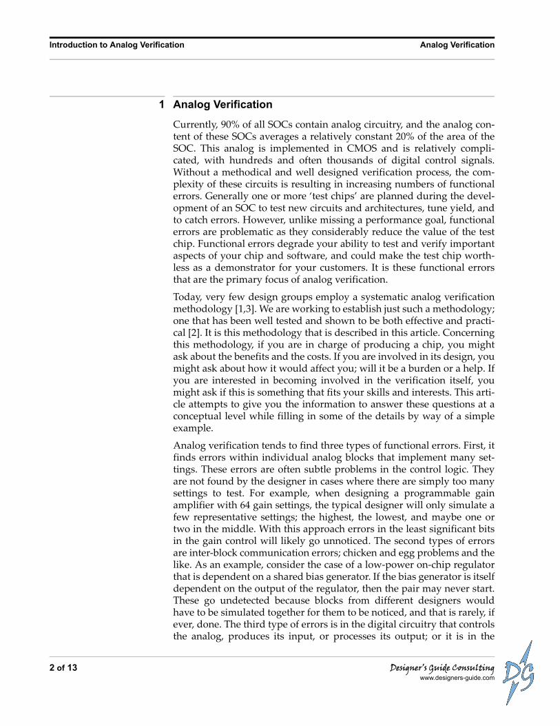
To see the importance of both, consider the equalizer shown below in Figure 1, as might be used as part of a high‐speed digital data transmis‐sion system. During the course of the design the equalizer itself must be verified to function correctly. In addition, usually it is desirable to build a model of the equalizer that can be used when verifying the overall sys‐tem. Analog verification fulfills both of these needs.
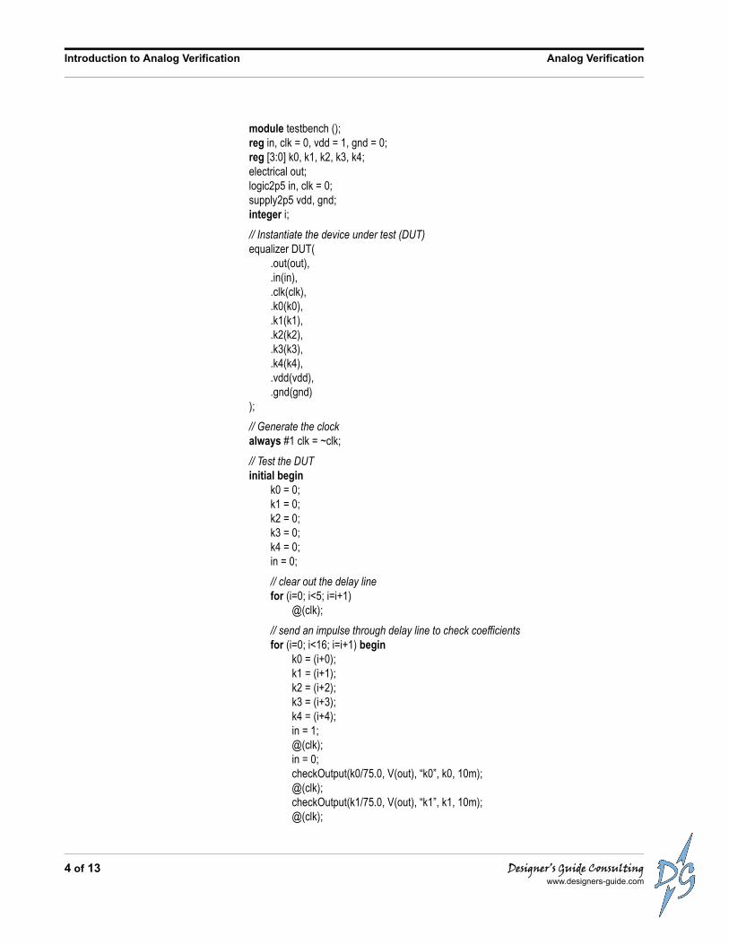
Writing an exhaustive equalizer test bench for a SPICE simulator would be very difficult, but Verilog‐AMS provides a rich language that can be used to easily describe the needed tests. An example is given below. It consists of 20‐30 lines of code that are tailored to the device under test and are used to thoroughly exercise it and confirm that it produces the expected output (for brevity, boilerplate code is not shown). The test bench operates by applying a unit impulse to the input, and then moni‐toring the output as the impulse propagates through the delay line. On the first clock cycle the output should produce k0, on the second k1, etc. After the unit impulse exits the delay line, the coefficients are changed and a new impulse is fed in. Notice that each coefficient is stepped through all of its 16 possible values, and each coefficient is always set differently from the others. This minimizes the likelihood that a wiring or logic error will be missed.
FIGURE 1 An equalizer used in digital data communication.
z–1
k0
Σ
in
out
k1 k2 k3 k4
z–1 z–1 z–1z–1
3 of 13Designer’s Guide Consultingwww.designers-guide.com
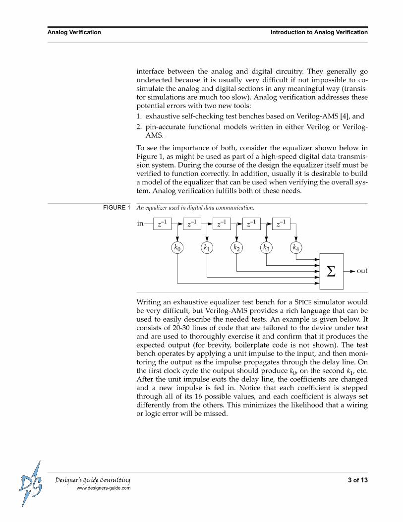
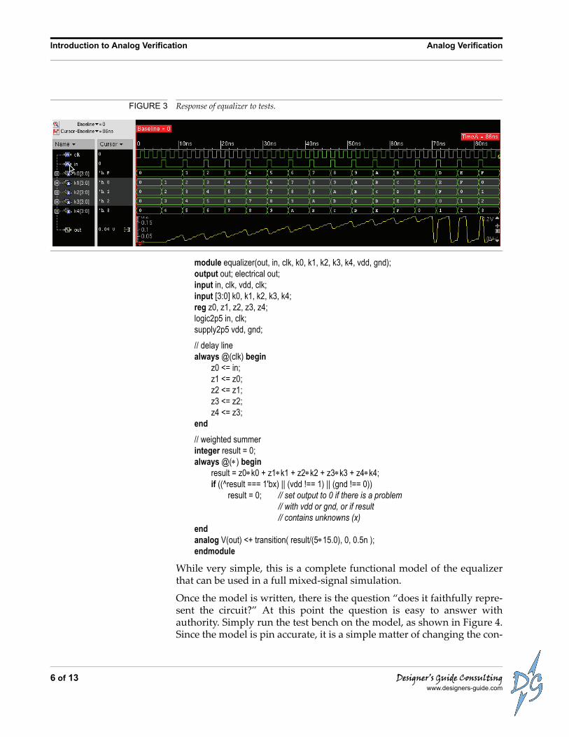
When run on the circuit as shown in Figure 2, the test bench produces the waveforms shown below in Figure 3. However, one does not need to actually view the waveforms to determine if the circuit is working cor‐rectly. This test bench runs 80 separate tests on the equalizer, all while driving each of the inputs independently through all possible values. When run on the circuit, it will produce a summary output that indicates which tests the circuit passed, and which it fails. If the test bench is writ‐ten exclusively from the functional specifications for the block, if the tests are comprehensive, and if they all pass, then the circuit implemen‐tation has been verified to be functionally equivalent to the specification. This in itself is generally much more verification than is done for analog blocks today. However, this is only the first of three sets of tests that are run, verifying that each individual analog or mixed‐signal block is implemented correctly. The next two sets will verify that the blocks oper‐ate together as expected and that the entire analog subsystem inter‐oper‐ates properly with the digital subsystem.
To take the next step, it is necessary to have a pin accurate functional model of each analog or mixed‐signal circuit block in the analog sub‐system. The model for our equalizer is shown below.
FIGURE 2 Testbench applied to schematic.
EqualizerSchematic
Equalizer Testbench
5 of 13Designer’s Guide Consultingwww.designers-guide.com
While very simple, this is a complete functional model of the equalizer that can be used in a full mixed‐signal simulation.
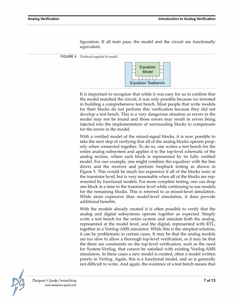
Once the model is written, there is the question “does it faithfully repre‐sent the circuit?” At this point the question is easy to answer with authority. Simply run the test bench on the model, as shown in Figure 4. Since the model is pin accurate, it is a simple matter of changing the con‐
FIGURE 3 Response of equalizer to tests.
6 of 13 Designer’s Guide Consultingwww.designers-guide.com
Analog Verification Introduction to Analog Verification
figuration. If all tests pass, the model and the circuit are functionally equivalent.
It is important to recognize that while it was easy for us to confirm that the model matched the circuit, it was only possible because we invested in building a comprehensive test bench. Most people that write models for their blocks do not perform this verification because they did not develop a test bench. This is a very dangerous situation as errors in the model may not be found and those errors may result in errors being injected into the implementation of surrounding blocks to compensate for the errors in the model.
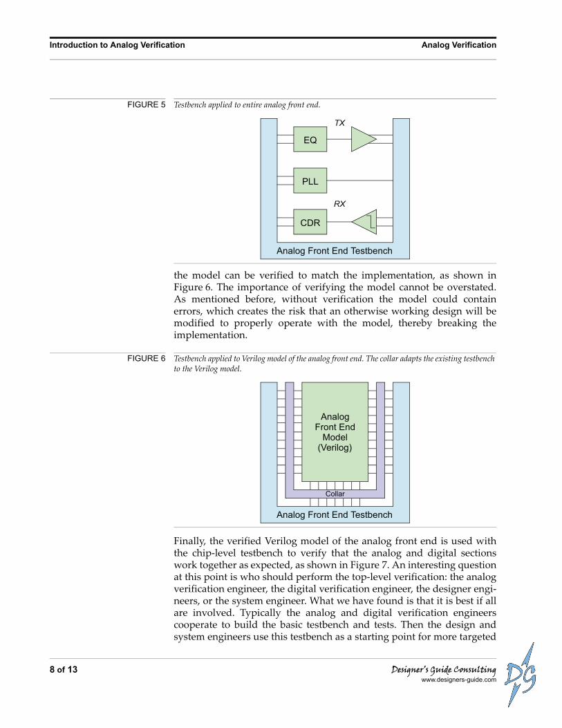
With a verified model of the mixed‐signal blocks, it is now possible to take the next step of verifying that all of the analog blocks operate prop‐erly when connected together. To do so, one writes a test bench for the entire analog subsystem and applies it to the top‐level schematic of the analog section, where each block is represented by its fully verified model. For our example, one might combine the equalizer with the line driver and the receiver and perform loopback testing as shown in Figure 5. This would be much too expensive if all of the blocks were at the transistor level, but is very reasonable when all of the blocks are rep‐resented by functional models. For more complete testing, one can drop one block at a time to the transistor level while continuing to use models for the remaining blocks. This is referred to as mixed‐level simulation. While more expensive than model‐level simulation, it does provide additional benefits.
With the models already created it is often possible to verify that the analog and digital subsystems operate together as expected. Simply write a test bench for the entire system and simulate both the analog, represented at the model level, and the digital, represented with RTL, together in a Verilog‐AMS simulator. While this is the simplest solution, it can be problematic in certain cases. It may be that the analog models are too slow to allow a thorough top‐level verification, or it may be that the there are constraints on the top‐level verification, such as the need for System‐Verilog, that cannot be satisfied with existing Verilog‐AMS simulators. In these cases a new model is created, often a model written purely in Verilog. Again, this is a functional model, and so is generally not difficult to write. And again, the existence of a test bench means that
FIGURE 4 Testbench applied to model.
EqualizerModel
Equalizer Testbench
7 of 13Designer’s Guide Consultingwww.designers-guide.com
Introduction to Analog Verification Analog Verification
the model can be verified to match the implementation, as shown in Figure 6. The importance of verifying the model cannot be overstated. As mentioned before, without verification the model could contain errors, which creates the risk that an otherwise working design will be modified to properly operate with the model, thereby breaking the implementation.
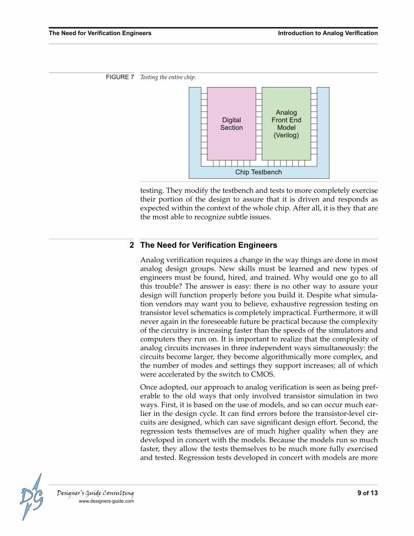
Finally, the verified Verilog model of the analog front end is used with the chip‐level testbench to verify that the analog and digital sections work together as expected, as shown in Figure 7. An interesting question at this point is who should perform the top‐level verification: the analog verification engineer, the digital verification engineer, the designer engi‐neers, or the system engineer. What we have found is that it is best if all are involved. Typically the analog and digital verification engineers cooperate to build the basic testbench and tests. Then the design and system engineers use this testbench as a starting point for more targeted
FIGURE 5 Testbench applied to entire analog front end.
FIGURE 6 Testbench applied to Verilog model of the analog front end. The collar adapts the existing testbench to the Verilog model.
CDR
EQ
PLL
Analog Front End Testbench
TX
RX
CollarCollar
Analog Front End Testbench
AnalogFront End
Model(Verilog)
8 of 13 Designer’s Guide Consultingwww.designers-guide.com
The Need for Verification Engineers Introduction to Analog Verification
testing. They modify the testbench and tests to more completely exercise their portion of the design to assure that it is driven and responds as expected within the context of the whole chip. After all, it is they that are the most able to recognize subtle issues.
2 The Need for Verification Engineers
Analog verification requires a change in the way things are done in most analog design groups. New skills must be learned and new types of engineers must be found, hired, and trained. Why would one go to all this trouble? The answer is easy: there is no other way to assure your design will function properly before you build it. Despite what simula‐tion vendors may want you to believe, exhaustive regression testing on transistor level schematics is completely impractical. Furthermore, it will never again in the foreseeable future be practical because the complexity of the circuitry is increasing faster than the speeds of the simulators and computers they run on. It is important to realize that the complexity of analog circuits increases in three independent ways simultaneously: the circuits become larger, they become algorithmically more complex, and the number of modes and settings they support increases; all of which were accelerated by the switch to CMOS.
Once adopted, our approach to analog verification is seen as being pref‐erable to the old ways that only involved transistor simulation in two ways. First, it is based on the use of models, and so can occur much ear‐lier in the design cycle. It can find errors before the transistor‐level cir‐cuits are designed, which can save significant design effort. Second, the regression tests themselves are of much higher quality when they are developed in concert with the models. Because the models run so much faster, they allow the tests themselves to be much more fully exercised and tested. Regression tests developed in concert with models are more
FIGURE 7 Testing the entire chip.
Chip Testbench
AnalogFront End
Model(Verilog)
DigitalSection
9 of 13Designer’s Guide Consultingwww.designers-guide.com
comprehensive and more sophisticated that those developed in concert with transistor‐level circuits alone.
To undertake this methodology one needs engineers trained in the art of analog functional modeling and testing and focused on verification. The alternative, using designers to both design and verify, is generally not as successful. It can be difficult to convince them to do it, they generally do not have the skills, and they tend to prioritize design activities over veri‐fication activities.
We have found that once an analog verification methodology is estab‐lished, it requires around one verification engineer for every five design engineers (a number that varies depending on the total number of modes and settings implemented by the circuit). Successful analog veri‐fication engineers need a variety of skills. They must have an analog background, meaning that they understand and are comfortable with analog circuits. They must be modeling engineers in that they must be facile with analog and digital modeling languages, such as Verilog‐AMS, and they must know how to write models and testbenches that are accu‐rate, robust, and efficient. They must be hackers in that they can quickly write scripts and develop work‐arounds to issues with the design tools. And finally, they must be verification engineers, meaning that they must be detail oriented as well as natural skeptics.
Analog verification engineers are currently very rare, and so must be developed. To that end, we provide both training and guidance as a way of helping to establish the discipline. Fortunately, being an analog verifi‐cation engineer is a desirable occupation. It is a creative endeavor that allows one to be involved in the design of analog integrated circuits, but provides more variety than if one were to design the individual blocks that make up the chip.
3 Adoption
Analog verification is a large change for design groups, and adopting it represents a substantial investment. Success in adopting the methodol‐ogy is assured only if the design company fully commits to it. As a result, it is almost always necessary that the change be driven from the top by the business owner; the one that both has the responsibility to deliver a working chip and authority to dedicate the needed resources. It is the desire to control the risk of a functional failure in the chip that drives adoption. However, the motivation to control this risk often only comes after a spectacular failure.
When first adopting an analog verification methodology, it is generally best to allow the verification effort to trail the design effort. The focus during this initial phase is on developing both expertise and a cache of
10 of 13 Designer’s Guide Consultingwww.designers-guide.com
models and testbenches that can be used on subsequent designs. It is during this phase that designers begin to first trust and later count on the verification engineers. It is also when the extent of the testing possi‐bilities starts to become clear. Designers have been so constrained in what they can test for so long, that it takes a while before the magnitude of the change really sinks in.
After the design and verification teams become comfortable with the analog verification methodology, and once a cache of models and test‐benches has been established, then it becomes possible for verification to actually lead design. The models, testbenches, and top‐level schematics are developed before the individual blocks are designed. In this way, verification can actually improve the efficiency of your design team. It does so by flushing out many of the errors and ambiguities in the speci‐fication and architecture before the expensive process of transistor‐level design begins. In this way, analog verification naturally leads to an increased use of top‐down design.
Another interesting side effect of adopting analog verification is that it tends to lead to healthier design teams. Analog verification provides a safety net that catches the errors of inexperienced design engineers mak‐ing it possible to build design teams from designers that have a range of experience levels. No longer is it necessary to limit yourselves to only hiring design engineers with five years experience, which greatly increases the pool of available engineers and allows engineers to develop naturally in your company, increasing retention.
Conclusion
Just as digital design did 15 years ago; analog design has now reached a transition. The move to CMOS has made analog circuits more function‐ally complex, and that complexity leads naturally to the need for analog functional verification. It is inevitable that all mixed‐signal system‐on‐chip design groups are destined to adopt analog verification. That being said, at this point it is not an easy transition. There are many barriers to be overcome and pitfalls to be avoided. It is easy to get frustrated and give up. However, know that it does work, and those that successfully adopt analog verification quickly reach the point where they cannot imagine designing without it. There are two factors that if present go a long way towards ensuring success in adopting analog verification: experience and commitment. We help companies transition to analog verification by providing experience in the form of training and guid‐ance. The commitment is up to you.
You can access a fully complete and executable version of this circuit and test bench at www.designers‐guide.com/newsletter/0807/example.tgz.
11 of 13Designer’s Guide Consultingwww.designers-guide.com
About The Authors Introduction to Analog Verification
About The Authors
Ken Kundert. Ken is an IEEE Fellow and co‐founded Designer’s Guide Consulting in 2005. From 1989 to 2005, Ken worked at Cadence Design Systems as a Fellow. Ken cre‐ated Spectre and was the principal architect of the Spectre circuit simulation family. As such, he has led the development of Spectre, SpectreHDL, and SpectreRF. He also played a key role in the development of Cadenceʹs AMS Designer and made substantial contri‐butions to both the Verilog‐AMS and VHDL‐AMS languages. While in school he authored Sparse, an industry standard sparse linear equation solver and created Agilent’s harmonic balance simulator. Before that Ken was a circuit designer at Tektronix and Hewlett‐Packard, and contributed to the design of the HP 8510 microwave network ana‐lyzer. He has written three books on circuit simulation: The Designerʹs Guide to Verilog‐AMS in 2004, The Designerʹs Guide to SPICE and Spectre in 1995, and Steady‐State Methods for Simulating Analog and Microwave Circuits in 1990; and created The Designerʹs Guide Community website. He has also authored eleven patents and over two‐dozen papers published in refereed conferences and journals.Ken received his Ph. D. in Electrical Engineering from the University of California at Ber‐keley in 1989, his M. Eng. degree in 1983 and his B. S. in 1979. Ken was elevated to the status of IEEE Fellow in January 2007 for contributions to simulation and modeling of analog, RF, and mixed‐signal circuits.
Henry Chang. Henry co‐founded Designer’s Guide Consulting in 2005. From 1995 to 2005, Henry worked at Cadence Design Systems, Inc. in research and development, methodology services, product marketing, corporate strategy, and in the office of the Chief Technology Officer. He has also worked at Micro Linear and GE Lighting. He is the author of three books: Winning the SoC Revolution: Experiences in Real Design in 2003, Sur‐viving the SoC Revolution: A Guide to Platform Based Design in 1999, and A Top‐Down, Con‐straint‐Driven Design Methodology for Analog Integrated Circuits in 1997. He is on the steering committee of the IEEE Custom Integrated Circuits Conference, serving pres‐ently as the general chairman. He holds 10 US patents, has authored 14 technical papers, and has participated at conferences giving tutorials, sitting on panels, and giving key‐note addresses.Henry received his Ph. D. and M. S. in Electrical Engineering from the University of Cal‐ifornia at Berkeley in 1994 and 1992 respectively. He received his Sc. B. degree in Electri‐cal Engineering from Brown University in 1989.
About Designer’s Guide ConsultingWe help design teams overcome difficult verification challenges. Those challenges can involve either functional or performance verification. A difficult functional verification problem might be assuring that a mixed‐signal circuit consisting of tens or hundreds of thousands of transistors with multiple ΔΣ converters operates correctly in each of its thousands of distinct operating modes. A difficult performance verification might be assuring that a large behaviorally complex circuit meets some demanding specification, such as a SerDes operating with a bit‐error rate of less than 10–18.
Designer’s Guide Consulting101 First Street, #150Los Altos, CA 94022+1 650-968-8291