+ All Categories
Home > Documents > ISSCC 2012 / SESSION 22 / IMAGE SENSORS / 22ericfossum.com/Publications/Papers/2012 ISSCC 1.5Mpixel...

ISSCC 2012 / SESSION 22 / IMAGE SENSORS / 22ericfossum.com/Publications/Papers/2012 ISSCC 1.5Mpixel...

Date post: 18-Feb-2018
Category:
Upload: doanque
View: 229 times
Download: 2 times
Share this document with a friend
3
392 2012 IEEE International Solid-State Circuits Conference ISSCC 2012 / SESSION 22 / IMAGE SENSORS / 22.7 22.7 A 1.5Mpixel RGBZ CMOS Image Sensor for Simultaneous Color and Range Image Capture Wonjoo Kim 1 , Wang Yibing 2 , Ilia Ovsiannikov 2 , SeungHoon Lee 1 , Yoondong Park 1 , Chilhee Chung 1 , Eric Fossum 1,2 1 Samsung Electronics, Hwasung, Korea 2 Samsung Semiconductor, Pasadena, CA A 1.5Mpixel RGBZ image sensor that simultaneously captures color (RGB) and time-of-flight (ToF) range (Z) images is presented. While ToF sensors are well documented [1,2], few, if any, monolithic sensors have been reported that cap- ture both range and color. In one sensor [3], a combined pixel structure captures color and range, but presumably in sequential fields. This approach does not allow simultaneous capturing of range with color, and the pixel performance cannot be optimized for each mode. In thie paper, we introduce a sensor that is designed to capture color and range simultaneously with individually optimized pixels. It is expected that future mobile-phone cameras and compact DSCs will be able to capture 3D still and video images, and permit gesture control of certain func- tions. ToF range sensing has several advantages over stereo-imaging or motion- computed 3D imaging, including single-lens implementation, less-intensive computing requirements, and freedom from occlusion artifacts. Monolithic inte- gration of color and ToF range sensing for a single-lens camera system is impor- tant for those consumer applications that require small-form-factor cameras with lowest-possible cost. In our sensor, color (RGB) and range (Z) pixels are tiled across the image plane. Our RGBZ sensor is modified from a 1920(H)×1080(V) 2Mpixel array of stan- dard 2.5T pixel RGBG color pixels with 2.25μm pitch. Every 3 rd row of color pix- els is replaced with a row of Z pixels. Each Z pixel is 2.25×9.0μm 2 . Thus the RGBZ kernel consists of two RGBG color kernels and one Z pixel. There are, in essence, two interlaced arrays: a 1920(H)×720(V) physical array of color pixels with an embedded 480(H)×360(V) array of range pixels for a total of 1.55Mpixels. A block diagram of the experimental sensor is shown in Fig. 22.7.1. The color pixels are driven from the left and read out at the top of the array. Range pixels are driven from the right and read out at the bottom. Column sig- nal lines are separate for color and range pixels. ADC and ToF signal processing is performed off-chip. Each Z pixel is a pinned photodiode with two transfer gates and two output ports [4,5]. For ranging, the scene is illuminated with 850nm NIR LEDs modulated at 20MHz. The two transfer gates TG1 and TG2 in the Z pixel are modulated 180° out of phase with each other at 20MHz. On one phase the optical signal is inte- grated on a floating diffusion (FD), and on the other phase the signal is discard- ed using a drain diffusion (DD). This single-tap mode of operation requires four fields to be collected, corresponding to the four quadrature phases. Each phase field is integrated and then read out. The LED modulation phase is shifted for each field. Our single-tap operation eases layout design and reduces fixed-pat- tern noise compared to traditional two-tap operation, but SNR is reduced by a factor of 2. Organization of the sensor into range-pixel “stripes” allows for easier routing of modulation-control lines to the range pixels and leads to less high-frequency- clock contamination of the color pixels. There are several tradeoffs in choosing the ratio of color-pixel rows to Z-pixel rows to optimize color and range image quality. For example, high ratios result in better color resolution but lower ToF signal SNR and hence less range accuracy. For this sensor, a ratio of 2:1 is cho- sen. Interpolating the missing stripes of color information to produce a 2Mpixel RGB image requires more sophisticated image signal processor (ISP) algo- rithms than conventional ones in RGBG sensor for removal of unwanted arti- facts. Initial ISP-algorithm results on simulated images show good results in suppressing many artifacts. Work on improved algorithms is ongoing. The major risk item explored in this work is the implementation and performance of relatively small Z pixels (2.25×9.0μm 2 ). Work to date has focused on the Z pix- els since the color pixels have commercial product heritage. Generally, smaller pixels collect fewer signal electrons, as with conventional image sensors. Commercial ToF imagers have typical pixel area in the 900-to-1,600μm 2 range but our pixels are 20μm 2 in area as drawn. Binning may be considered to boost SNR at the cost of reduced resolution if needed. As of the submission date, CFA and microlenses have not yet been applied to the RGBZ pixels. However, a second risk with the interlaced architecture is the absence of a global narrowband NIR filter. Color pixels should not be exposed to NIR light, and range pixels should not be exposed to visible light. Visible light contamination in the Z pixels is suppressed using a commercially available visi- ble-light-blocking filter and normal ToF signal-processing methods. To date, pixel-wise NIR-block filter technology for the color pixels is not satisfactory. In our frontside-illuminated (FSI) sensor, the Z pixels extend laterally under the RGB pixels to collect NIR-generated photoelectrons. A special deep implant under the RGB pixels separates the visible (vertical) from NIR (lateral) carrier collection regions. Figure 22.7.2 explains how the implant extends the effective area of the Z pixels to about 6.75×9.0μm 2 and reduces unwanted NIR signal in the color pixels. The degree of lateral extension depends on the device epi-layer thickness. Currently it is just 3.0μm, so the lateral extension effect is small. Suppression of residual NIR “fogging” of the color pixels is performed by the ISP using the NIR signal collected by the Z pixel as reference. Simulations show that good NIR fog suppression is possible. A different approach for backside illu- minated RGBZ sensors is under separate investigation. Readout electronics for this small sensor are kept as simple as possible as shown in Fig. 22.7.3. The circuits resemble those used in early CMOS image sensor prototypes, which is useful for ToF range imaging [6]. Due to their low level of sophistication, analog readout speeds for the sensor are low: about 1Mpixel/s. The experimental sensor is fabricated in a 0.13μm FSI CMOS image sensor process, with a few additional implant steps. A sample range image is shown in Fig. 22.7.4. Range linearity and error are shown in Fig. 22.7.5. A table compar- ing the performance of the embedded range sensor to other reported range sen- sors is shown in Fig. 22.7.6. A die micrograph is shown in Fig. 22.7.7. It is seen that despite the small drawn Z-pixel size, performance of the embed- ded range sensor, without binning or Gaussian-kernel convolution, is compara- ble to range sensors with larger-sized pixels, and that the sensor has sufficient performance to enable many applications. Future work will need to show that the modeled NIR fog correction algorithms yield the anticipated performance. However, at this time we are greatly encouraged by the ISP simulations and experimental results obtained with the exploratory RGBZ sensor. References: [1] R. Miyagawa and T. Kanade, “CCD-based range finding sensor,” IEEE Trans. Electron Devices, vol. 44, no. 10, pp. 1648-1652, 1997. [2] R. Lange, et al., “Demodulation Pixels in CCD and CMOS Technologies for Time-of-Flight Ranging”, Proc. of SPIE, vol. 3965A, pp. 177, 2000. [3] S.J. Kim, J. Kim, S.W. Han, B.M. Kang, K.C. Lee, and C-Y Kim, “A 640×480 Image Sensor with Unified Pixel Architecture for 2D/3D Imaging in 0.11μm CMOS”, IEEE Symp. VLSI Circuits, pp. 92-93, June 2011. [4] V. Berezin, A. Krymski, and E.R. Fossum, “Lock-In Pinned Photodiode Photodetector,” US Patent No. 6,239,456, 2001. [5] D. Stoppa, et al., “A Range Image Sensor Based on 10μm Lock-In Pixels in 0.18μm CMOS Imaging Technology,” IEEE J. Solid-State Circuits, vol. 46, no. 1, pp. 248-258, Jan. 2011. [6] T.-Y. Lee, et al., “Dark Current Suppression During High Speed Photogate Modulation for 3D ToF Imaging Pixel,” Proc. Int. Image Sensor Workshop, June 2011. 978-1-4673-0377-4/12/$31.00 ©2012 IEEE
Transcript

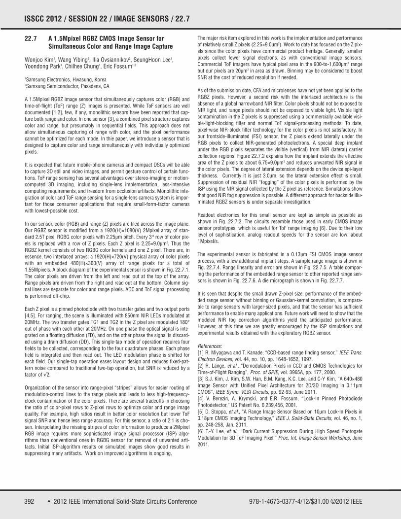
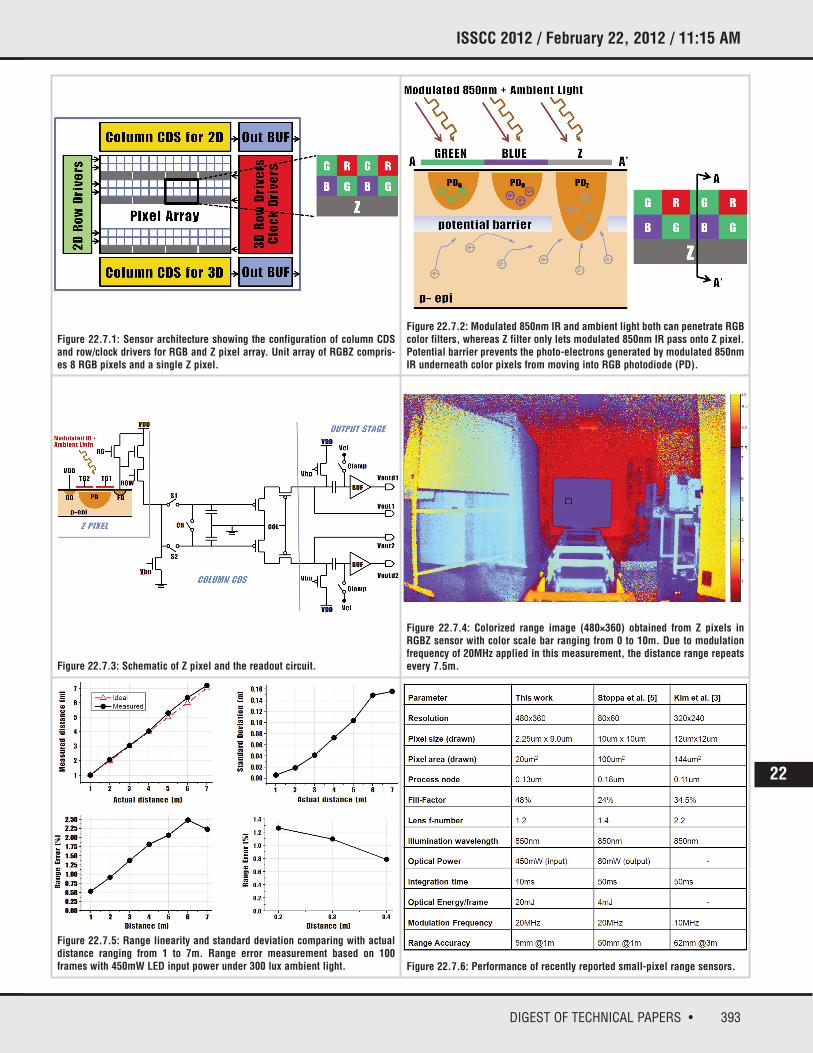
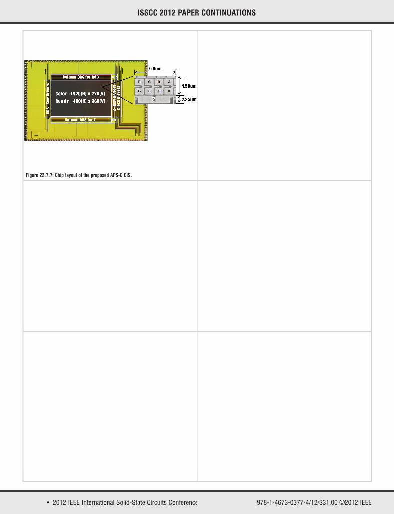
392 • 2012 IEEE International Solid-State Circuits Conference

ISSCC 2012 / SESSION 22 / IMAGE SENSORS / 22.7

22.7 A 1.5Mpixel RGBZ CMOS Image Sensor for Simultaneous Color and Range Image Capture

Wonjoo Kim1, Wang Yibing2, Ilia Ovsiannikov2, SeungHoon Lee1, Yoondong Park1, Chilhee Chung1, Eric Fossum1,2

1Samsung Electronics, Hwasung, Korea2Samsung Semiconductor, Pasadena, CA

A 1.5Mpixel RGBZ image sensor that simultaneously captures color (RGB) andtime-of-flight (ToF) range (Z) images is presented. While ToF sensors are welldocumented [1,2], few, if any, monolithic sensors have been reported that cap-ture both range and color. In one sensor [3], a combined pixel structure capturescolor and range, but presumably in sequential fields. This approach does notallow simultaneous capturing of range with color, and the pixel performancecannot be optimized for each mode. In thie paper, we introduce a sensor that isdesigned to capture color and range simultaneously with individually optimizedpixels.

It is expected that future mobile-phone cameras and compact DSCs will be ableto capture 3D still and video images, and permit gesture control of certain func-tions. ToF range sensing has several advantages over stereo-imaging or motion-computed 3D imaging, including single-lens implementation, less-intensivecomputing requirements, and freedom from occlusion artifacts. Monolithic inte-gration of color and ToF range sensing for a single-lens camera system is impor-tant for those consumer applications that require small-form-factor cameraswith lowest-possible cost.

In our sensor, color (RGB) and range (Z) pixels are tiled across the image plane.Our RGBZ sensor is modified from a 1920(H)×1080(V) 2Mpixel array of stan-dard 2.5T pixel RGBG color pixels with 2.25µm pitch. Every 3rd row of color pix-els is replaced with a row of Z pixels. Each Z pixel is 2.25×9.0µm2. Thus theRGBZ kernel consists of two RGBG color kernels and one Z pixel. There are, inessence, two interlaced arrays: a 1920(H)×720(V) physical array of color pixelswith an embedded 480(H)×360(V) array of range pixels for a total of1.55Mpixels. A block diagram of the experimental sensor is shown in Fig. 22.7.1.The color pixels are driven from the left and read out at the top of the array.Range pixels are driven from the right and read out at the bottom. Column sig-nal lines are separate for color and range pixels. ADC and ToF signal processingis performed off-chip.

Each Z pixel is a pinned photodiode with two transfer gates and two output ports[4,5]. For ranging, the scene is illuminated with 850nm NIR LEDs modulated at20MHz. The two transfer gates TG1 and TG2 in the Z pixel are modulated 180°out of phase with each other at 20MHz. On one phase the optical signal is inte-grated on a floating diffusion (FD), and on the other phase the signal is discard-ed using a drain diffusion (DD). This single-tap mode of operation requires fourfields to be collected, corresponding to the four quadrature phases. Each phasefield is integrated and then read out. The LED modulation phase is shifted foreach field. Our single-tap operation eases layout design and reduces fixed-pat-tern noise compared to traditional two-tap operation, but SNR is reduced by afactor of √2.

Organization of the sensor into range-pixel “stripes” allows for easier routing ofmodulation-control lines to the range pixels and leads to less high-frequency-clock contamination of the color pixels. There are several tradeoffs in choosingthe ratio of color-pixel rows to Z-pixel rows to optimize color and range imagequality. For example, high ratios result in better color resolution but lower ToFsignal SNR and hence less range accuracy. For this sensor, a ratio of 2:1 is cho-sen. Interpolating the missing stripes of color information to produce a 2MpixelRGB image requires more sophisticated image signal processor (ISP) algo-rithms than conventional ones in RGBG sensor for removal of unwanted arti-facts. Initial ISP-algorithm results on simulated images show good results insuppressing many artifacts. Work on improved algorithms is ongoing.

The major risk item explored in this work is the implementation and performanceof relatively small Z pixels (2.25×9.0µm2). Work to date has focused on the Z pix-els since the color pixels have commercial product heritage. Generally, smallerpixels collect fewer signal electrons, as with conventional image sensors.Commercial ToF imagers have typical pixel area in the 900-to-1,600µm2 rangebut our pixels are 20µm2 in area as drawn. Binning may be considered to boostSNR at the cost of reduced resolution if needed.

As of the submission date, CFA and microlenses have not yet been applied to theRGBZ pixels. However, a second risk with the interlaced architecture is theabsence of a global narrowband NIR filter. Color pixels should not be exposed toNIR light, and range pixels should not be exposed to visible light. Visible lightcontamination in the Z pixels is suppressed using a commercially available visi-ble-light-blocking filter and normal ToF signal-processing methods. To date,pixel-wise NIR-block filter technology for the color pixels is not satisfactory. Inour frontside-illuminated (FSI) sensor, the Z pixels extend laterally under theRGB pixels to collect NIR-generated photoelectrons. A special deep implantunder the RGB pixels separates the visible (vertical) from NIR (lateral) carriercollection regions. Figure 22.7.2 explains how the implant extends the effectivearea of the Z pixels to about 6.75×9.0µm2 and reduces unwanted NIR signal inthe color pixels. The degree of lateral extension depends on the device epi-layerthickness. Currently it is just 3.0µm, so the lateral extension effect is small.Suppression of residual NIR “fogging” of the color pixels is performed by theISP using the NIR signal collected by the Z pixel as reference. Simulations showthat good NIR fog suppression is possible. A different approach for backside illu-minated RGBZ sensors is under separate investigation.

Readout electronics for this small sensor are kept as simple as possible asshown in Fig. 22.7.3. The circuits resemble those used in early CMOS imagesensor prototypes, which is useful for ToF range imaging [6]. Due to their lowlevel of sophistication, analog readout speeds for the sensor are low: about1Mpixel/s.

The experimental sensor is fabricated in a 0.13µm FSI CMOS image sensorprocess, with a few additional implant steps. A sample range image is shown inFig. 22.7.4. Range linearity and error are shown in Fig. 22.7.5. A table compar-ing the performance of the embedded range sensor to other reported range sen-sors is shown in Fig. 22.7.6. A die micrograph is shown in Fig. 22.7.7.

It is seen that despite the small drawn Z-pixel size, performance of the embed-ded range sensor, without binning or Gaussian-kernel convolution, is compara-ble to range sensors with larger-sized pixels, and that the sensor has sufficientperformance to enable many applications. Future work will need to show that themodeled NIR fog correction algorithms yield the anticipated performance.However, at this time we are greatly encouraged by the ISP simulations andexperimental results obtained with the exploratory RGBZ sensor.

References:[1] R. Miyagawa and T. Kanade, “CCD-based range finding sensor,” IEEE Trans.Electron Devices, vol. 44, no. 10, pp. 1648-1652, 1997.[2] R. Lange, et al., “Demodulation Pixels in CCD and CMOS Technologies forTime-of-Flight Ranging”, Proc. of SPIE, vol. 3965A, pp. 177, 2000.[3] S.J. Kim, J. Kim, S.W. Han, B.M. Kang, K.C. Lee, and C-Y Kim, “A 640×480Image Sensor with Unified Pixel Architecture for 2D/3D Imaging in 0.11µmCMOS”, IEEE Symp. VLSI Circuits, pp. 92-93, June 2011.[4] V. Berezin, A. Krymski, and E.R. Fossum, “Lock-In Pinned PhotodiodePhotodetector,” US Patent No. 6,239,456, 2001.[5] D. Stoppa, et al., “A Range Image Sensor Based on 10µm Lock-In Pixels in0.18µm CMOS Imaging Technology,” IEEE J. Solid-State Circuits, vol. 46, no. 1,pp. 248-258, Jan. 2011.[6] T.-Y. Lee, et al., “Dark Current Suppression During High Speed PhotogateModulation for 3D ToF Imaging Pixel,” Proc. Int. Image Sensor Workshop, June2011.

978-1-4673-0377-4/12/$31.00 ©2012 IEEE

393DIGEST OF TECHNICAL PAPERS •

ISSCC 2012 / February 22, 2012 / 11:15 AM

Figure 22.7.1: Sensor architecture showing the configuration of column CDSand row/clock drivers for RGB and Z pixel array. Unit array of RGBZ compris-es 8 RGB pixels and a single Z pixel.

Figure 22.7.2: Modulated 850nm IR and ambient light both can penetrate RGBcolor filters, whereas Z filter only lets modulated 850nm IR pass onto Z pixel.Potential barrier prevents the photo-electrons generated by modulated 850nmIR underneath color pixels from moving into RGB photodiode (PD).

Figure 22.7.3: Schematic of Z pixel and the readout circuit.

Figure 22.7.5: Range linearity and standard deviation comparing with actualdistance ranging from 1 to 7m. Range error measurement based on 100frames with 450mW LED input power under 300 lux ambient light. Figure 22.7.6: Performance of recently reported small-pixel range sensors.

Figure 22.7.4: Colorized range image (480×360) obtained from Z pixels inRGBZ sensor with color scale bar ranging from 0 to 10m. Due to modulationfrequency of 20MHz applied in this measurement, the distance range repeatsevery 7.5m.

22

• 2012 IEEE International Solid-State Circuits Conference 978-1-4673-0377-4/12/$31.00 ©2012 IEEE

ISSCC 2012 PAPER CONTINUATIONS

Figure 22.7.7: Chip layout of the proposed APS-C CIS.


Recommended