17
McMaster – France cooperation in condensed matter physics (some examples) Jean-Pierre Landesman, Physics and Photonics University Rennes-1, France [email protected]
McMaster – France cooperation in
condensed matter physics (some examples)
Jean-Pierre Landesman, Physics and Photonics
University Rennes-1, France

Objectives Outline:
- Overview of the cooperation between McMaster and French universities /
CNRS in the field of condensed matter physics
- Joint work on neutron scattering and crystal growth (McMaster – EU)
Bruce Gaulin, McMaster
- Joint work on thin film technologies for opto-electronic and photonic
applications (McMaster – Rennes 1 – CNRS) Jean-Pierre Landesman,
Rennes

Collaboration between McMaster and condensed matter physics
groups in France
This has been particularly active for more than 30 years.
Key groups in France which have historically contributed to this collaboration:
Grenoble, Lyon, Orsay (now Paris-Saclay)
More recently: Rennes

In February 2018 McMaster organized the 1st joint workshop with the French
Centre National de la Recherche Scientifique (CNRS)
This 3-days workshop received support and funding from the CNRS Bureau in
Washington (Dr X. Morise) and from the French Embassy in Ottawa (Dr A.
Rauzy)
Attendees from France: about 30 from different places, working in different
fields including condensed matter physics, chemistry, mathematics, …
The 2nd workshop took place in Grenoble, in July 2019. During this workshop,
discussions with the CNRS started to consider establishing an International
Research Network between French groups and Southern-Ontario universities.
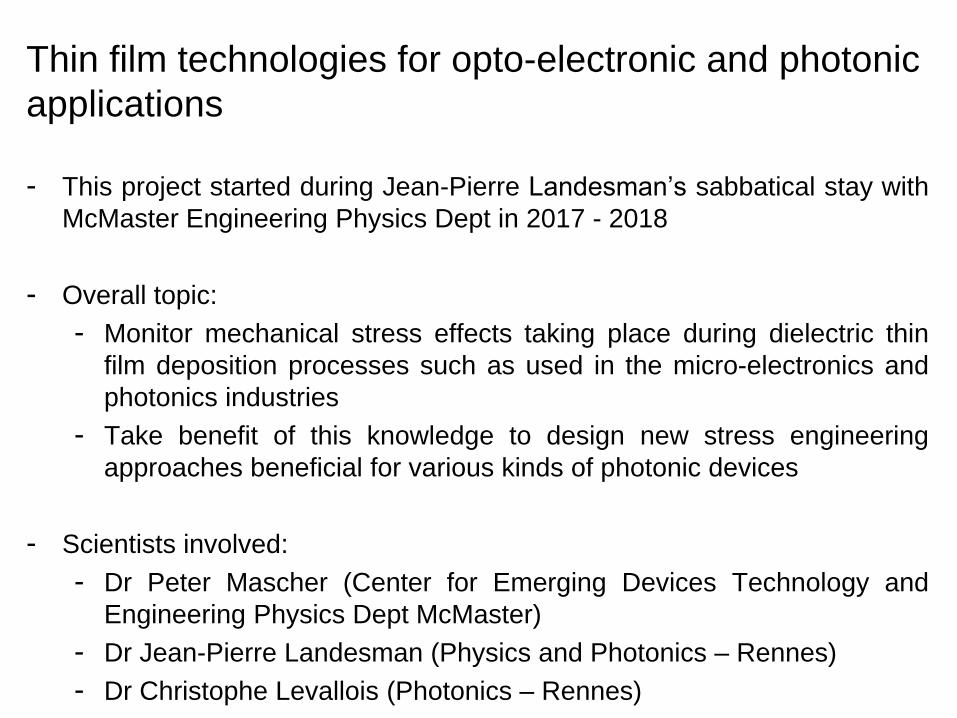
Thin film technologies for opto-electronic and photonic
applications
- This project started during Jean-Pierre Landesman’s sabbatical stay with
McMaster Engineering Physics Dept in 2017 - 2018
- Overall topic:
- Monitor mechanical stress effects taking place during dielectric thin
film deposition processes such as used in the micro-electronics and
photonics industries
- Take benefit of this knowledge to design new stress engineering
approaches beneficial for various kinds of photonic devices
- Scientists involved:
- Dr Peter Mascher (Center for Emerging Devices Technology and
Engineering Physics Dept McMaster)
- Dr Jean-Pierre Landesman (Physics and Photonics – Rennes)
- Dr Christophe Levallois (Photonics – Rennes)
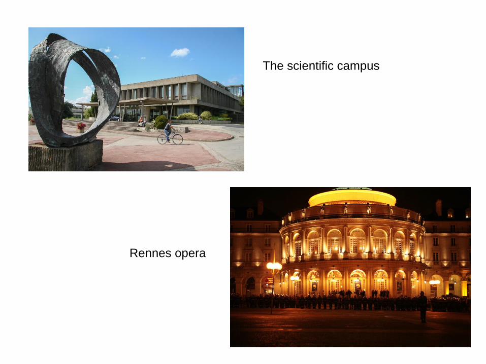
The scientific campus
Rennes opera

Objectives Why is mechanical stress a hot topic for
semiconductor devices ?
First of all, mechanical stress at any level in semiconductor devices is a
RELIABILITY concern

A study on the impact of localized stresses in the various materials that
constitute “Via hole” structures in Si on the leakage current in a test device
N Ranganathan, K Prasad, N Balasubramanian, K L Pey, J. Micromech.
Microeng. 18 (2008)

Dislocation generation in Si due to mechanical stress build-up underneath a
LOCOS area. The dislocations are concentrated in zones where the shear
stress is important.
I. De Wolf, Spectroscopy Europe 15/2 (2003)

Strained materials are also introduced deliberately in some semiconductor
devices resulting in improved properties (carrier mobility in Si, efficiency of
III-V semiconductor laser diodes)
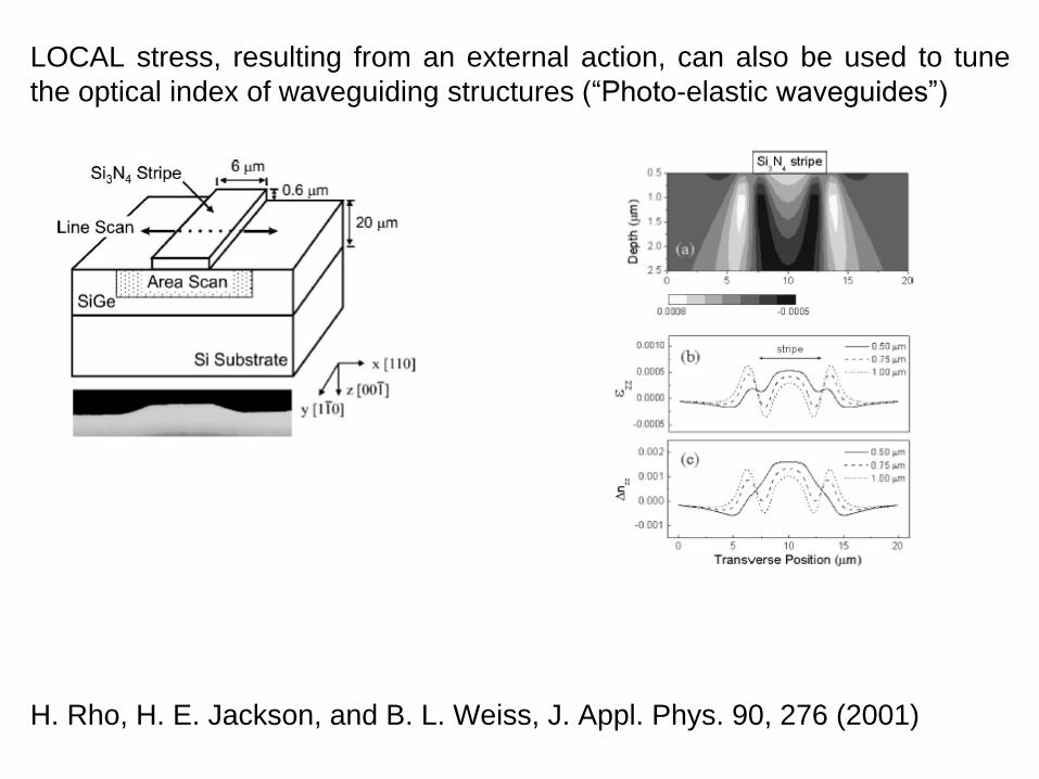
LOCAL stress, resulting from an external action, can also be used to tune
the optical index of waveguiding structures (“Photo-elastic waveguides”)
H. Rho, H. E. Jackson, and B. L. Weiss, J. Appl. Phys. 90, 276 (2001)
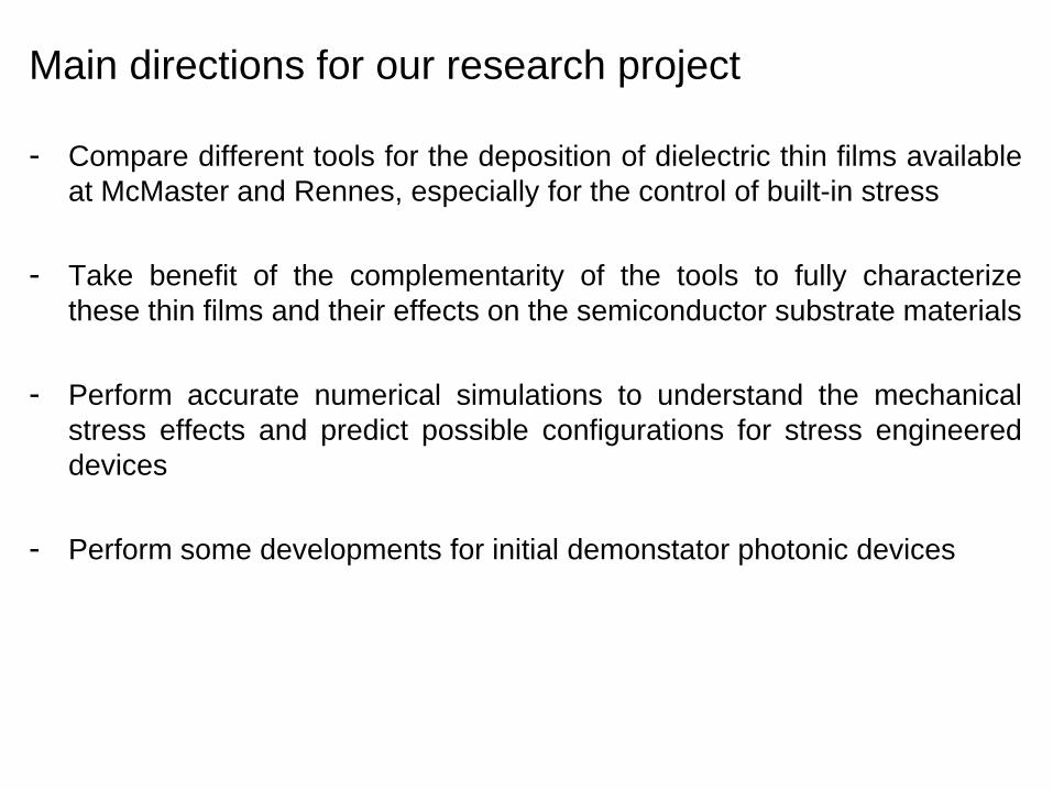
Main directions for our research project
- Compare different tools for the deposition of dielectric thin films available
at McMaster and Rennes, especially for the control of built-in stress
- Take benefit of the complementarity of the tools to fully characterize
these thin films and their effects on the semiconductor substrate materials
- Perform accurate numerical simulations to understand the mechanical
stress effects and predict possible configurations for stress engineered
devices
- Perform some developments for initial demonstator photonic devices
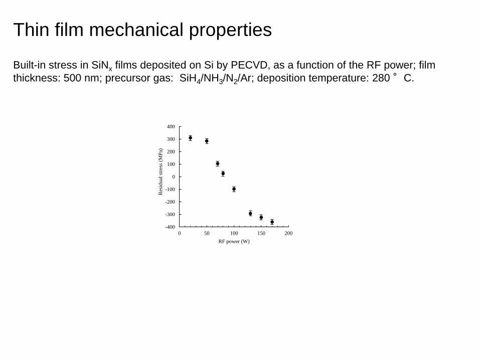
Thin film mechanical properties
Built-in stress in SiNx films deposited on Si by PECVD, as a function of the RF power; film
thickness: 500 nm; precursor gas: SiH4/NH3/N2/Ar; deposition temperature: 280 °C.
-400
-300
-200
-100
0
100
200
300
400
0 50 100 150 200
Res
idu
al s
tres
s (M
Pa)
RF power (W)
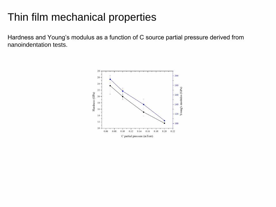
Thin film mechanical properties
Hardness and Young’s modulus as a function of C source partial pressure derived from
nanoindentation tests.

Deformation field induced in the semiconductor
material substrate by the dielectric thin film
Photoluminescence maps showing the crystal deformation field generated in an InP substrate
by a 20 µm – wide SiNx dielectric stripe with compressive built-in stress
Tools which we have activitated for this cooperation and beyond
French Canada Research Fund (French Embassy)
ANR – NSERC joint call for proposals, including companies from France and Canada
(unsuccessful …)
Co-supervised (co-tutelle) PhD student presently in Rennes, about to move to McMaster, with joint
funding from Rennes and McMaster
Erasmus + project led by Rennes:
- 5 teaching visits to Rennes for professors from McMaster since 2019
- 2 teaching visits to McMaster for professors from Rennes since 2019
- 2 undergraduate students from McMaster hosted in Rennes for research interships in 2019 (+
2 scheduled in 2020)
- 1 undergraduate student from Rennes hosted at McMaster for research internship in 2020
Outside the Erasmus + project, other undergraduate students are regularly hosted by McMaster
professors for internships (4 to 6 per year since 2018)


