8. What are three applications of multiplexers? 9. Name an application of demultiplexers. 10. How many control lines are needed for a 16 input multiplexer? In this lab exercise you will begin your study of M5I ,. circuits. In LAB EXERCISE 9.1 this'lab exercise you Will also study the 4-line to .l0-line decoder. Decoders This circuit is often used as a BCD to decimal decoder. It can also Objectives be used as a decoder for any number of binary inputs less than four such as 3-line to 8-line decoders and 2-line to 4-line decoders. .' , LD-2 Logic Designer Materials 74L5424-Line to la-Line Decoder Jumper Wires . TTL Data Book 1. Wire 051 DE and 052 DE to 5 VOC. Now wire the circuit Procedure shown in Figure 9-12. This is the circuit for a BCD/DEC decoder. 195
Transcript
8. What are three applications ofmultiplexers?
9. Name an application of demultiplexers.
10. How many control lines are needed for a 16 input multiplexer?
In this lab exercise you will begin your study of M5I ,. circuits. In LAB EXERCISE 9.1 this ' lab exercise you Will also study the 4-line to. l0-line decoder. Decoders This circuit is often used as a BCD to decimal decoder. It can also
Objectivesbe used as a decoder for any number of binary inputs less than four such as 3-line to 8-line decoders and 2-line to 4-line decoders.
.' , LD-2 Logic Designer Materials
74L5424-Line to la-Line Decoder
Jumper Wires
. TTL Data Book
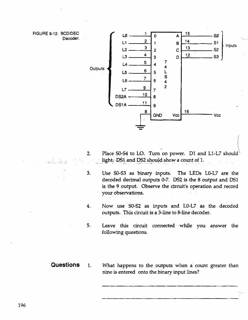
1. Wire 051 DE and 052 DE to 5 VOC. Now wire the circuit Procedure shown in Figure 9-12. This is the circuit for a BCD/DEC decoder.
195
FIGURE 9-12. BCDIDEC Decoder.
Outputs
L0
L1
L2
L3
L4
L5
1
2
3
4
5
6
L6 7
L7
DS2A
9
10
DS1A 11
8-,
-- -
0 A
1 B
2 C
3
4
5
6
7
7 4 L S 4 2
D
8
9
GND Vee
15
14 Inputs
13
12
16 Vcc
2. Place SO-S4 to La. Tum on power. 01 and LJ-L7 ShOUIJ . ..' light~· D5~ , and P52 should showac0llnt of 1
3. UseSO-53 as binary inputs. The LEOs LO-L7are the decoded decilnal outputsQ.;;7. 052 is the 8 output and 051 is the 9 output. ' Observe the cirCUit's operation and record yoUr observations.
4. Now use SO-52 as inputs and LO-L7 as the decoded outputs. This circuit is a 3-line to B-line decoder.
5. Leave this circuit connected ·while you answer the following questions.
Questions 1. What happens to the outputs when ' a count greater than nine is entered onto the binary input lines?
196
2. What type of circuit could you use to tell that an invalid input had been entered on the SO-S3 inputs?
3. What type of circui~ would you need to use to detect invalid inputs for the3-lineto 8-line 'decOder?
4. Are the outputs ofthe 74LS42 LO true or HI true?
5. The LD-2 has an: internal display driver so that the outputs of fhe 74LS42 ' are driVing ' a TIL load and not a directly connected LED. Can the 74LS42 be uSed to drive an' LED indicator directly? Explain your answer., "
In this lab exercise you will investigate the use of the 7447 BCDT~SEVEN-SEGMENT DECODERS/DRIVERS. You will also learn about the ..use of seven-segment displays. You will study implementing simple displays.
LAB EXERCISE 9.2 Decoder/Drivers
Objectives
LD-2 Logic Designer
7447 BCD-T~7-Segment Decoders/Drivers
Materials
TTL 312 Common-Anode 7-Segment Display
Jumper Wires
197
330 Ohm Resistors (7)
Tn Data Book
Procedure 1. You will study the seven-segment LED display in the first part of this lab. Place the TIL 312 onto the LD-s breadboard.
2. ' Wire pin 14 to +5 VDC. Connect one end of a 330 ohm to ground and use the , other, end to detennir\~~! and' record the basing diagram for the Tn 312. Noconnectlon. is made for pins 4,5 and 12. N()tice that the Tn 312 is a commol1 anode display and that 7-segment displays are also available in a common cathode configuration. Also note that the display segments are labeled clock-wise from the top as a-:f. The seventh segment ,is label~d as g and is the cross segment. Many of these displays have left and right decimal pOints. Some have the ability to display a leading minus sign. Seven-segment displays' are often used to fo small arrays of , decimal digits. " The display
, implem ted here is a ~ingle digit decimal display. A full digit d· display can display aI'l:Y number 0;9. A halfdigit can only display a blank or a, one. Simple sevensegment displays can be made using LCD technology as well as LED technology.
'
3. Wire the circuit shown in Figure 9-13. Vee
FIGURE 9-13. BCOn-Segment SO ___7-f A a ~1_3_J' .......----14 \,.....---~ a I---~
Decoder. Anodes12 13 b. , S1 """" B 7 b. -~-I.': ." :, ."J;': '/~' .' . J" -~., .: ; T.4 . j~. .1G' {~ , ~ ;; . ,2" 11S2-----I C 4 e L
7 8~6 10S3 __---I 30 d : v-------,t d 1
9 7 . 8 2e
2
14 11
15
g v------Ig 3300 (7)
168 GNO Vee
-Vee-
198
4. Turn SO-S3 to LO. 01 should light and a zero should be shown in the 7-segment display. Use SO-53 as the A-O inputs and the display as the output. Observe and record the operation of this circuit. Compare this display circuit to the one used on the LO-2 and note differences.
5. ... Leave this circui~ · following questions.
c:6npected while you answer the
1. Is the display clear? How could this be improved? Questions
2. What is the purpose of the 330 ohm resistors?
3. What count is displayed when~L 312 consumes the greatest power?
4. . What input is required to blank the display?
The purpose of this lab exe~cise is to ~veStlgate encoders. You LAB EXERCISE 9.3 will study the 74L5148 €ight-line-t<ttJ:rree-line encoder. This Encoders type of encoder is also known as an octal encoder. It could be used to encode an octal keypad or to convert octal to binary. Objectives
LO-2 Logic Oesigner Materials
74LS148 8-Line to 3-Line Priority Encoder
199
Procedure
. FIGURE 9-14. B-Line to 3-Line Encoder.
Jumper Wires
TIL Data Book
1. Place the 74L5148 onto the LD-2 breadboard. Connect power and ground to the 74LSl48.
2. Wire the circuit shown in Figure 9-14. This is the 8-line to 3-line encoder.
50 10
11
12
13
1
2
3
4
5 8
0
1
2
3
4
5
A2
6
7
E1
GND Vcc ~
6
7 7
4 A1 L 5 AO 9
1 -
4 8
G5 14
L251
52 LI
\ :: 53
L7 56
57
Vcc-= 3. Place SO-57 to HI. Tum on power. D1 and LO-U will light.
4. Use SO-57 as inputs and LO-L3 and L7 as outputs. Observe ... and.r~ord .the 8peratio,~ of thisciI:cuit. Pay attention to . wkrhapperis when morEnHan·'oneiilputiSLO~ i ...
5. Leave this Circuit cormected and answer the following questi6ns~ ' .,
Questions 1. Are the inputs to the 74LSl48 LO true or HI true?
200
2. Are the outputs · used in this experiment LO true or HI true?
3. Explain what is meant by a priority encoder?
4. How can you tell the difference ,between a zero input and no input?
In this Jab exercise you will study digital ~ultj.Flexers. The LAB EXERCISE 9.4 74~S153 4-line tQ., ,I-line qata . selector / mulqplexer will be Digital Multiplexers studied. A multiple'xer can be used as a datas,elector or for parallel to serial conversion. A multiplexer can alSo be used to implement logic · functions. ~e following: lab exercise will familiarize you with the operation of the 4-line to I-line multiplexer. Objectives ·
LD-2 Logic Designer Materials
74LS153 ..
4-Line to I-Line Data Selectors/Multiplexers
Jumper Wires
TIL Data Book
1. Place the 74LS153 on the LD-2 breadboard. and ground to the circuit.
Wire power Procedure
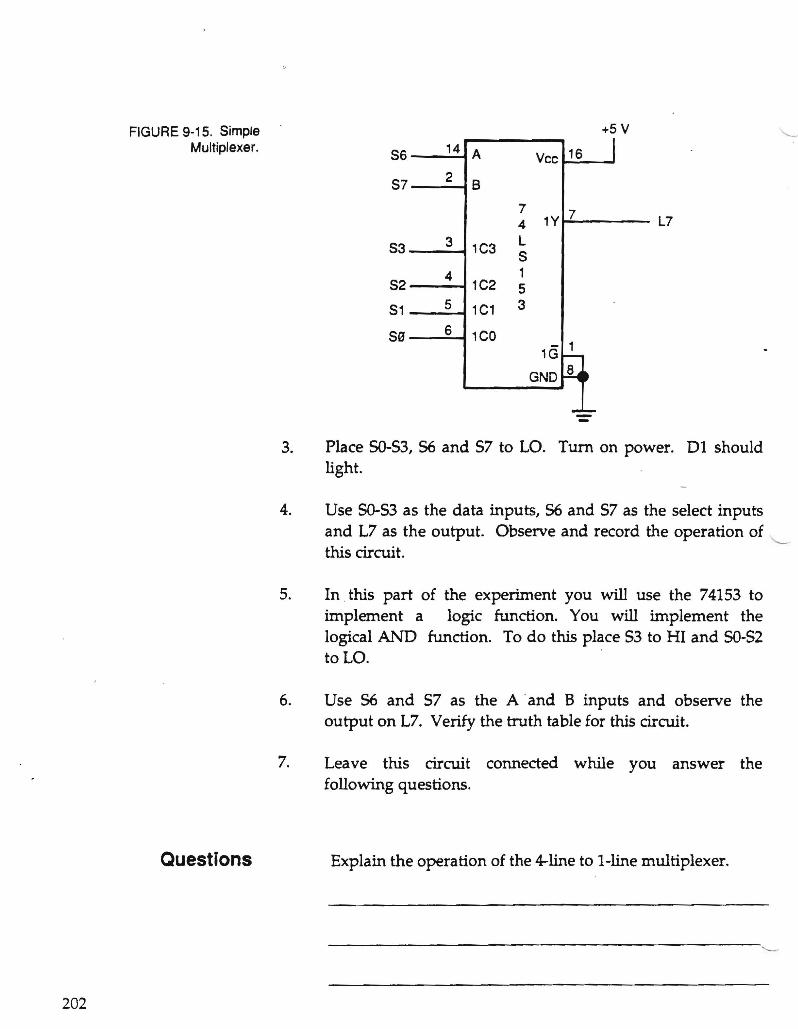
2. Wire the circuit shown in Figure 9-15. simple multiplexer.
This circuit is a
201
FIGURE 9-15. Simple Multiplexer.
3.
4.
5.
6.
7.
Questions
+5V
S6
S7
l7
S3
S2
S1
S0
14
2
3
4
5
6
A
B
7 4
1C3 L S 1
1C2 5
1C1 3
1CO
Vee 16 J
1Y 7
1<3 1 ~
GND r§.O
.....---Place 50-53, 56 and 57 to LO. Turn on power. D1 should light.
Use 50-53 as the data inputs, 56 and 57 as the select inputs and L7 as the output. Observe and record the operation of '-this circuit.
In . this part of the experiment you will use the 74153 to implement a logic function. You will implement the logical AND function. To do this place 53 to HI and SO-52 toLD.
Use 56 and 57 as the A . and B inputs and observe the output on L7. Verify the truth table for this circuit.
Leave this circuit connected while you answer the following questions.
Explain the operation of the 4-line to 1-line multiplexer.
202
2. How wquld you implement the logical EXNOR using a -74LS153?
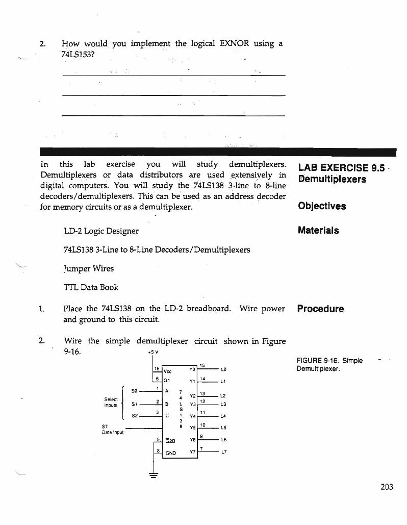
In this lab exercise you will study demultiplexers. Demultiplexers or data distributors , are used ,extensively in digital computerS. You will study the 74LS138 3-line to 8-line decoders/demultiplexers. This can be' used as an address decoder for memory circuits or as a demultiplexer.
LD-2 Logic Designer
74LS138 3-Line to 8-Line Decoders/Demultiplexers
Jumper Wires
TIL Data Book
1. Place the 74LS138 on the LD-2 breadboard. Wire power and ground to this circuit.
2. Wire the simple demultiplexer circuit shown in Figure 9-16. +5 v
15 YO LOVee~
14G1 Y1...!.. L1
1SO A 7 13Y2 L24 12Select { 2S1 L3B L Y3Inputs
S 113 1S2 L4C Y4 3
10S7 8 Y5 L5 Data Input
9Y6 L6..2.. G2B
7Y7 L7GND~
' -
LAB EXERCISE 9.5 Bemultip1exers
Objectives
Materials
Procedure
FIGURE 9-16. Simple Demultiplexer.
203
3. This circuIt is a basic decoder cb-cuit with additionil1 gating for enabling the circuitry. Any decoder with one-or more enable inputs can be used as a demultiplexer. Use 50- 52 as the select inputs, 57 as the data input and LO-L7 as the outputs. Observe the circuit operation and record your observations. Pay attention to the state of unselected outputs.
4. Leave this circuit assembled as you answer the following ... ~ : . questiQ~. . ", .':
; .. ' : • j ,I . r~-~-~ " . I .~:: '
Questions 1. 5ince the demultiplexer is , the mverse function of 'the multiplexer, could the 74LS138 be used for serial to parallel conversion? ' .
2. What type of circuit is a demultiplexer made from?


![EDS Demobilization Tabletop Exercise [Exercise Location] [Exercise Date] [Insert Logo Here]](https://static.documents.pub/doc/80x56/56649e865503460f94b898d0/eds-demobilization-tabletop-exercise-exercise-location-exercise-date-insert.jpg)


![[EXERCISE NAME} Player Briefing [Exercise Date] Player Briefing [Exercise Date]](https://static.documents.pub/doc/80x56/56649ee65503460f94bf6431/exercise-name-player-briefing-exercise-date-player-briefing-exercise-date.jpg)
![EDS Security Tabletop Exercise [Exercise Location] [Exercise Date] [Insert Logo Here]](https://static.documents.pub/doc/80x56/56649dbb5503460f94aac3ec/eds-security-tabletop-exercise-exercise-location-exercise-date-insert.jpg)


