40
LAMPIRAN A DATA SHEET KOMPONEN

LAMPIRAN A
DATA SHEET KOMPONEN
8-bit Microcontroller with 8K Bytes Flash
AT89C52
Features• Compatible with MCS-51™ Products• 8K Bytes of In-System Reprogrammable Flash Memory• Endurance: 1,000 Write/Erase Cycles• Fully Static Operation: 0 Hz to 24 MHz• Three-level Program Memory Lock• 256 x 8-bit Internal RAM• 32 Programmable I/O Lines• Three 16-bit Timer/Counters• Eight Interrupt Sources• Programmable Serial Channel• Low-power Idle and Power-down Modes
DescriptionThe AT89C52 is a low-power, high-performance CMOS 8-bit microcomputer with 8Kbytes of Flash programmable and erasable read only memory (PEROM). The deviceis manufactured using Atmel’s high-density nonvolatile memory technology and iscompatible with the industry-standard 80C51 and 80C52 instruction set and pinout.The on-chip Flash allows the program memory to be reprogrammed in-system or by aconventional nonvolatile memory programmer. By combining a versatile 8-bit CPUwith Flash on a monolithic chip, the Atmel AT89C52 is a powerful microcomputerwhich provides a highly-flexible and cost-effective solution to many embedded controlapplications.
1
Rev. 0313H–02/00
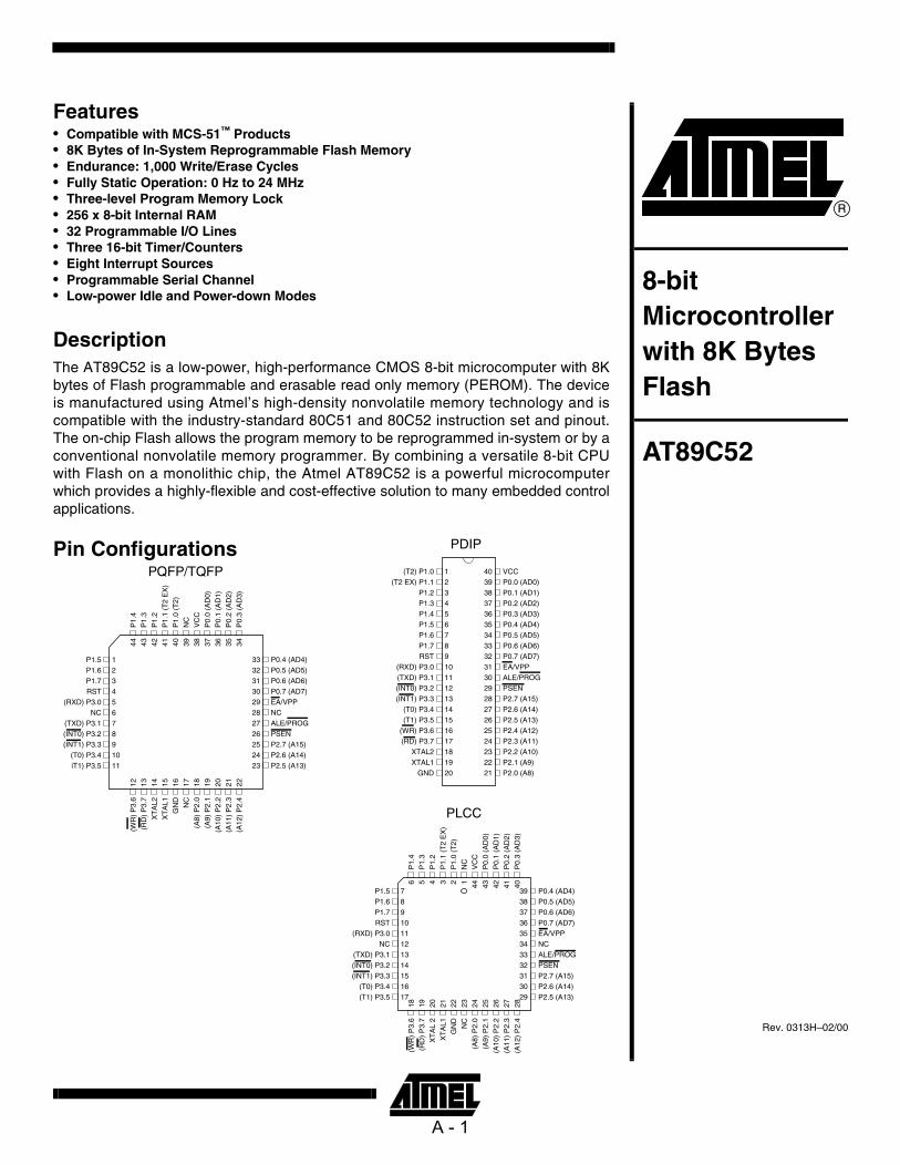
Pin ConfigurationsPQFP/TQFP
1234567891011
3332313029282726252423
P1.5P1.6P1.7RST
(RXD) P3.0NC
(TXD) P3.1(INT0) P3.2(INT1) P3.3
(T0) P3.4iT1) P3.5
P0.4 (AD4)P0.5 (AD5)P0.6 (AD6)P0.7 (AD7)EA/VPPNCALE/PROGPSENP2.7 (A15)P2.6 (A14)P2.5 (A13)
44 43 42 41 40 39 38 37 36 35 34
12 13 14 15 16 17 18 19 20 21 22
(WR
) P
3.6
(RD
) P
3.7
XT
AL2
XT
AL1
GN
DN
C(A
8) P
2.0
(A9)
P2.
1(A
10)
P2.
2(A
11)
P2.
3(A
12)
P2.
4
P1.
4P
1.3
P1.
2P
1.1
(T2
EX
)P
1.0
(T2)
NC
VC
CP
0.0
(AD
0)P
0.1
(AD
1)P
0.2
(AD
2)P
0.3
(AD
3)
PDIP
1234567891011121314151617181920
4039383736353433323130292827262524232221
(T2) P1.0(T2 EX) P1.1
P1.2P1.3P1.4P1.5P1.6P1.7RST
(RXD) P3.0(TXD) P3.1(INT0) P3.2(INT1) P3.3
(T0) P3.4(T1) P3.5
(WR) P3.6(RD) P3.7
XTAL2XTAL1
GND
VCCP0.0 (AD0)P0.1 (AD1)P0.2 (AD2)P0.3 (AD3)P0.4 (AD4)P0.5 (AD5)P0.6 (AD6)P0.7 (AD7)EA/VPPALE/PROGPSENP2.7 (A15)P2.6 (A14)P2.5 (A13)P2.4 (A12)P2.3 (A11)P2.2 (A10)P2.1 (A9)P2.0 (A8)
PLCC
7891011121314151617
3938373635343332313029
P1.5P1.6P1.7RST
(RXD) P3.0NC
(TXD) P3.1(INT0) P3.2(INT1) P3.3
(T0) P3.4(T1) P3.5
P0.4 (AD4)P0.5 (AD5)P0.6 (AD6)P0.7 (AD7)EA/VPPNCALE/PROGPSENP2.7 (A15)P2.6 (A14)P2.5 (A13)
6 5 4 3 2 1 44 43 42 41 40
18 19 20 21 22 23 24 25 26 27 28
(WR
) P
3.6
(RD
) P
3.7
XT
AL
2X
TA
L1G
ND
NC
(A8)
P2.
0(A
9) P
2.1
(A10
) P
2.2
(A11
) P
2.3
(A12
) P
2.4
P1.
4P
1.3
P1.
2P
1.1
(T2
EX
)P
1.0
(T2)
NC
VC
CP
0.0
(AD
0)P
0.1
(AD
1)P
0.2
(AD
2)P
0.3
(AD
3)
A - 1
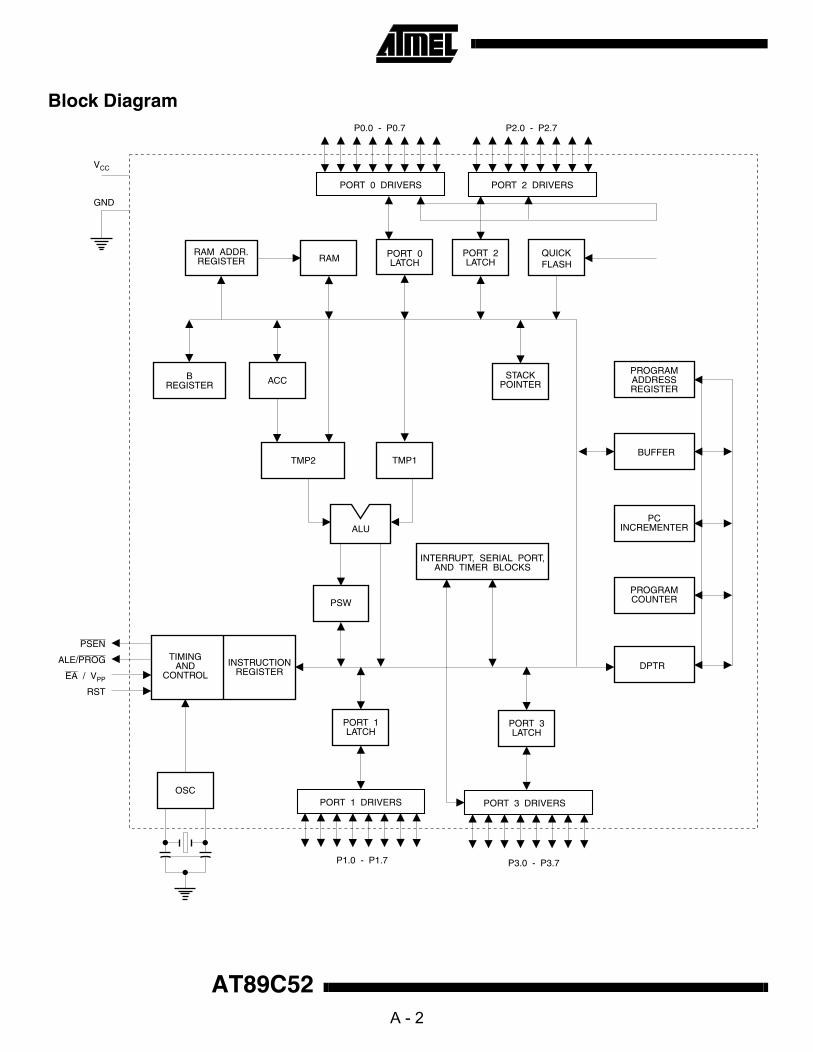
Block Diagram
PORT 2 DRIVERS
PORT 2LATCH
P2.0 - P2.7
QUICKFLASH
PORT 0LATCHRAM
PROGRAMADDRESSREGISTER
BUFFER
PCINCREMENTER
PROGRAMCOUNTER
DPTR
RAM ADDR.REGISTER
INSTRUCTIONREGISTER
BREGISTER
INTERRUPT, SERIAL PORT,AND TIMER BLOCKS
STACKPOINTERACC
TMP2 TMP1
ALU
PSW
TIMINGAND
CONTROL
PORT 3LATCH
PORT 3 DRIVERS
P3.0 - P3.7
PORT 1LATCH
PORT 1 DRIVERS
P1.0 - P1.7
OSC
GND
VCC
PSEN
ALE/PROG
EA / VPP
RST
PORT 0 DRIVERS
P0.0 - P0.7
AT89C52A - 2

AT89C52
The AT89C52 provides the following standard features: 8Kbytes of Flash, 256 bytes of RAM, 32 I/O lines, three 16-bittimer/counters, a six-vector two-level interrupt architecture,a full-duplex serial port, on-chip oscillator, and clock cir-cuitry. In addition, the AT89C52 is designed with static logicfor operation down to zero frequency and supports twosoftware selectable power saving modes. The Idle Modestops the CPU while allowing the RAM, timer/counters,serial port, and interrupt system to continue functioning.The Power-down mode saves the RAM contents butfreezes the oscillator, disabling all other chip functions untilthe next hardware reset.
Pin DescriptionVCCSupply voltage.
GNDGround.
Port 0
Port 0 is an 8-bit open drain bi-directional I/O port. As anoutput port, each pin can sink eight TTL inputs. When 1sare written to port 0 pins, the pins can be used as high-impedance inputs.
Port 0 can also be configured to be the multiplexed low-order address/data bus during accesses to external pro-gram and data memory. In this mode, P0 has internalpullups.
Port 0 also receives the code bytes during Flash program-ming and outputs the code bytes dur ing programverification. External pullups are required during programverification.
Port 1
Port 1 is an 8-bit bi-directional I/O port with internal pullups.The Port 1 output buffers can sink/source four TTL inputs.When 1s are written to Port 1 pins, they are pulled high bythe internal pullups and can be used as inputs. As inputs,Port 1 pins that are externally being pulled low will sourcecurrent (IIL) because of the internal pullups.
In addition, P1.0 and P1.1 can be configured to be thetimer/counter 2 external count input (P1.0/T2) and thetimer/counter 2 trigger input (P1.1/T2EX), respectively, asshown in the following table.Port 1 also receives the low-order address bytes duringFlash programming and verification.
Port 2Port 2 is an 8-bit bi-directional I/O port with internal pullups.The Port 2 output buffers can sink/source four TTL inputs.When 1s are written to Port 2 pins, they are pulled high bythe internal pullups and can be used as inputs. As inputs,Port 2 pins that are externally being pulled low will sourcecurrent (IIL) because of the internal pullups.
Port 2 emits the high-order address byte during fetchesfrom external program memory and during accesses toexternal data memory that use 16-bit addresses (MOVX @DPTR). In this application, Port 2 uses strong internal pul-lups when emitting 1s. During accesses to external datamemory that use 8-bit addresses (MOVX @ RI), Port 2emits the contents of the P2 Special Function Register.
Port 2 also receives the high-order address bits and somecontrol signals during Flash programming and verification.
Port 3Port 3 is an 8-bit bi-directional I/O port with internal pullups.The Port 3 output buffers can sink/source four TTL inputs.When 1s are written to Port 3 pins, they are pulled high bythe internal pullups and can be used as inputs. As inputs,Port 3 pins that are externally being pulled low will sourcecurrent (IIL) because of the pullups.
Port 3 also serves the functions of various special featuresof the AT89C51, as shown in the following table.
Port 3 also receives some control signals for Flash pro-gramming and verification.
RSTReset input. A high on this pin for two machine cycles whilethe oscillator is running resets the device.
ALE/PROGAddress Latch Enable is an output pulse for latching thelow byte of the address during accesses to external mem-ory. This pin is also the program pulse input (PROG) duringFlash programming.
In normal operation, ALE is emitted at a constant rate of 1/6the oscillator frequency and may be used for external
Port Pin Alternate Functions
P1.0 T2 (external count input to Timer/Counter 2), clock-out
P1.1 T2EX (Timer/Counter 2 capture/reload trigger anddirection control)
Port Pin Alternate Functions
P3.0 RXD (serial input port)
P3.1 TXD (serial output port)
P3.2 INT0 (external interrupt 0)
P3.3 INT1 (external interrupt 1)
P3.4 T0 (timer 0 external input)
P3.5 T1 (timer 1 external input)
P3.6 WR (external data memory write strobe)
P3.7 RD (external data memory read strobe)
A - 3

timing or clocking purposes. Note, however, that one ALEpulse is skipped during each access to external datamemory.
If desired, ALE operation can be disabled by setting bit 0 ofSFR location 8EH. With the bit set, ALE is active only dur-ing a MOVX or MOVC instruction. Otherwise, the pin isweakly pulled high. Setting the ALE-disable bit has noeffect if the microcontroller is in external execution mode.
PSENProgram Store Enable is the read strobe to external pro-gram memory.
When the AT89C52 is executing code from external pro-gram memory, PSEN is activated twice each machinecycle, except that two PSEN activations are skipped duringeach access to external data memory.
EA/VPPExternal Access Enable. EA must be strapped to GND inorder to enable the device to fetch code from external pro-gram memory locations starting at 0000H up to FFFFH.Note, however, that if lock bit 1 is programmed, EA will beinternally latched on reset.
EA should be strapped to VCC for internal programexecutions.
This pin also receives the 12-volt programming enable volt-age (VPP) during Flash programming when 12-voltprogramming is selected.
XTAL1Input to the inverting oscillator amplifier and input to theinternal clock operating circuit.
XTAL2Output from the inverting oscillator amplifier.
Table 1. AT89C52 SFR Map and Reset Values
0F8H 0FFH
0F0HB
000000000F7H
0E8H 0EFH
0E0HACC
000000000E7H
0D8H 0DFH
0D0HPSW
000000000D7H
0C8HT2CON
00000000T2MOD
XXXXXX00RCAP2L00000000
RCAP2H00000000
TL200000000
TH200000000
0CFH
0C0H 0C7H
0B8HIP
XX0000000BFH
0B0HP3
111111110B7H
0A8HIE
0X0000000AFH
0A0HP2
111111110A7H
98HSCON
00000000SBUF
XXXXXXXX9FH
90HP1
1111111197H
88HTCON
00000000TMOD
00000000TL0
00000000TL1
00000000TH0
00000000TH1
000000008FH
80HP0
11111111SP
00000111DPL
00000000DPH
00000000PCON
0XXX000087H
AT89C52A - 4

AT89C52
Special Function RegistersA map of the on-chip memory area called the Special Func-tion Register (SFR) space is shown in Table 1.
Note that not all of the addresses are occupied, and unoc-cupied addresses may not be implemented on the chip.Read accesses to these addresses will in general returnrandom data, and write accesses will have an indetermi-nate effect.
User software should not write 1s to these unlisted loca-tions, since they may be used in future products to invoke
new features. In that case, the reset or inactive values ofthe new bits will always be 0.
Timer 2 Registers Control and status bits are contained inregisters T2CON (shown in Table 2) and T2MOD (shown inTable 4) for Timer 2. The register pair (RCAP2H, RCAP2L)are the Capture/Reload registers for Timer 2 in 16-bit cap-ture mode or 16-bit auto-reload mode.
Interrupt Registers The individual interrupt enable bits arein the IE register. Two priorities can be set for each of thesix interrupt sources in the IP register.r
Data MemoryThe AT89C52 implements 256 bytes of on-chip RAM. Theupper 128 bytes occupy a parallel address space to theSpecial Function Registers. That means the upper 128bytes have the same addresses as the SFR space but arephysically separate from SFR space.
When an instruction accesses an internal location aboveaddress 7FH, the address mode used in the instruction
specifies whether the CPU accesses the upper 128 bytesof RAM or the SFR space. Instructions that use directaddressing access SFR space.
For example, the following direct addressing instructionaccesses the SFR at location 0A0H (which is P2).
MOV 0A0H, #data
Table 2. T2CON – Timer/Counter 2 Control Registe
T2CON Address = 0C8H Reset Value = 0000 0000B
Bit Addressable
Bit TF2 EXF2 RCLK TCLK EXEN2 TR2 C/T2 CP/RL2
7 6 5 4 3 2 1 0
Symbol Function
TF2 Timer 2 overflow flag set by a Timer 2 overflow and must be cleared by software. TF2 will not be set when either RCLK = 1 or TCLK = 1.
EXF2 Timer 2 external flag set when either a capture or reload is caused by a negative transition on T2EX and EXEN2 = 1. When Timer 2 interrupt is enabled, EXF2 = 1 will cause the CPU to vector to the Timer 2 interrupt routine. EXF2 must be cleared by software. EXF2 does not cause an interrupt in up/down counter mode (DCEN = 1).
RCLK Receive clock enable. When set, causes the serial port to use Timer 2 overflow pulses for its receive clock in serial port Modes 1 and 3. RCLK = 0 causes Timer 1 overflow to be used for the receive clock.
TCLK Transmit clock enable. When set, causes the serial port to use Timer 2 overflow pulses for its transmit clock in serial port Modes 1 and 3. TCLK = 0 causes Timer 1 overflows to be used for the transmit clock.
EXEN2 Timer 2 external enable. When set, allows a capture or reload to occur as a result of a negative transition on T2EX if Timer 2 is not being used to clock the serial port. EXEN2 = 0 causes Timer 2 to ignore events at T2EX.
TR2 Start/Stop control for Timer 2. TR2 = 1 starts the timer.
C/T2 Timer or counter select for Timer 2. C/T2 = 0 for timer function. C/T2 = 1 for external event counter (falling edge triggered).
CP/RL2 Capture/Reload select. CP/RL2 = 1 causes captures to occur on negative transitions at T2EX if EXEN2 = 1. CP/RL2 = 0 causes automatic reloads to occur when Timer 2 overflows or negative transitions occur at T2EX when EXEN2 = 1. When either RCLK or TCLK = 1, this bit is ignored and the timer is forced to auto-reload on Timer 2 overflow.
A - 5
Instructions that use indirect addressing access the upper128 bytes of RAM. For example, the following indirectaddressing instruction, where R0 contains 0A0H, accessesthe data byte at address 0A0H, rather than P2 (whoseaddress is 0A0H).
MOV @R0, #data
Note that stack operations are examples of indirectaddressing, so the upper 128 bytes of data RAM are avail-able as stack space.
Timer 0 and 1Timer 0 and Timer 1 in the AT89C52 operate the same wayas Timer 0 and Timer 1 in the AT89C51.
Timer 2Timer 2 is a 16-bit Timer/Counter that can operate as eithera timer or an event counter. The type of operation isselected by bit C/T2 in the SFR T2CON (shown in Table 2).Timer 2 has three operating modes: capture, auto-reload(up or down counting), and baud rate generator. Themodes are selected by bits in T2CON, as shown in Table 3.
Timer 2 consists of two 8-bit registers, TH2 and TL2. In theTimer function, the TL2 register is incremented everymachine cycle. Since a machine cycle consists of 12 oscil-lator periods, the count rate is 1/12 of the oscillatorfrequency.
In the Counter function, the register is incremented inresponse to a 1-to-0 transition at its corresponding external
input pin, T2. In this function, the external input is sampledduring S5P2 of every machine cycle. When the samplesshow a high in one cycle and a low in the next cycle, thecount is incremented. The new count value appears in theregister during S3P1 of the cycle following the one in whichthe transition was detected. Since two machine cycles (24oscillator periods) are required to recognize a 1-to-0 transi-tion, the maximum count rate is 1/24 of the oscillatorfrequency. To ensure that a given level is sampled at leastonce before it changes, the level should be held for at leastone full machine cycle.
Capture ModeIn the capture mode, two options are selected by bitEXEN2 in T2CON. If EXEN2 = 0, Timer 2 is a 16-bit timeror counter which upon overflow sets bit TF2 in T2CON.This bit can then be used to generate an interrupt. IfEXEN2 = 1, Timer 2 performs the same operation, but a 1-to-0 transition at external input T2EX also causes the cur-rent value in TH2 and TL2 to be captured into RCAP2H andRCAP2L, respectively. In addition, the transition at T2EXcauses bit EXF2 in T2CON to be set. The EXF2 bit, likeTF2, can generate an interrupt. The capture mode is illus-trated in Figure 1.
Auto-reload (Up or Down Counter)Timer 2 can be programmed to count up or down whenconfigured in its 16-bit auto-reload mode. This feature isinvoked by the DCEN (Down Counter Enable) bit located inthe SFR T2MOD (see Table 4). Upon reset, the DCEN bitis set to 0 so that timer 2 will default to count up. WhenDCEN is set, Timer 2 can count up or down, depending onthe value of the T2EX pin.
Table 3. Timer 2 Operating Modes
RCLK +TCLK CP/RL2 TR2 MODE
0 0 1 16-bit Auto-reload
0 1 1 16-bit Capture
1 X 1 Baud Rate Generator
X X 0 (Off)
AT89C52A - 6

AT89C52
Figure 1. Timer in Capture Mode
Figure 2 shows Timer 2 automatically counting up whenDCEN = 0. In this mode, two options are selected by bitEXEN2 in T2CON. If EXEN2 = 0, Timer 2 counts up to0FFFFH and then sets the TF2 bit upon overflow. Theoverflow also causes the timer registers to be reloaded withthe 16-bit value in RCAP2H and RCAP2L. The values inTimer in Capture ModeRCAP2H and RCAP2L are presetby software. If EXEN2 = 1, a 16-bit reload can be triggeredeither by an overflow or by a 1-to-0 transition at externalinput T2EX. This transition also sets the EXF2 bit. Both theTF2 and EXF2 bits can generate an interrupt if enabled.
Setting the DCEN bit enables Timer 2 to count up or down,as shown in Figure 3. In this mode, the T2EX pin controls
the direction of the count. A logic 1 at T2EX makes Timer 2count up. The timer will overflow at 0FFFFH and set theTF2 bit. This overflow also causes the 16-bit value inRCAP2H and RCAP2L to be reloaded into the timer regis-ters, TH2 and TL2, respectively.
A logic 0 at T2EX makes Timer 2 count down. The timerunderflows when TH2 and TL2 equal the values stored inRCAP2H and RCAP2L. The underflow sets the TF2 bit andcauses 0FFFFH to be reloaded into the timer registers.
The EXF2 bit toggles whenever Timer 2 overflows orunderflows and can be used as a 17th bit of resolution. Inthis operating mode, EXF2 does not flag an interrupt.
OSC
EXF2T2EX PIN
T2 PIN
TR2
EXEN2
C/T2 = 0
C/T2 = 1
CONTROL
CAPTURE
OVERFLOW
CONTROL
TRANSITIONDETECTOR TIMER 2
INTERRUPT
÷12
RCAP2LRCAP2H
TH2 TL2 TF2
A - 7
Figure 2. Timer 2 Auto Reload Mode (DCEN = 0)
Table 4. T2MOD – Timer 2 Mode Control Register
T2MOD Address = 0C9H Reset Value = XXXX XX00B
Not Bit Addressable
– – – – – – T2OE DCEN
Bit 7 6 5 4 3 2 1 0
Symbol Function
– Not implemented, reserved for future
T2OE Timer 2 Output Enable bit.
DCEN When set, this bit allows Timer 2 to be configured as an up/down counter.
OSC
EXF2
TF2
T2EX PIN
T2 PIN
TR2
EXEN2
C/T2 = 0
C/T2 = 1
CONTROL
RELOAD
OVERFLOW
CONTROL
TRANSITIONDETECTOR
TIMER 2INTERRUPT
÷12
RCAP2LRCAP2H
TH2 TL2
AT89C52A - 8

AT89C52
Figure 3. Timer 2 Auto Reload Mode (DCEN = 1)
Figure 4. Timer 2 in Baud Rate Generator Mode
OSC
EXF2
TF2
T2EX PIN
COUNTDIRECTION1=UP0=DOWN
T2 PIN
TR2CONTROL
OVERFLOW
(DOWN COUNTING RELOAD VALUE)
(UP COUNTING RELOAD VALUE)
TOGGLE
TIMER 2INTERRUPT
12
RCAP2LRCAP2H
0FFH0FFH
TH2 TL2
C/T2 = 0
C/T2 = 1
÷
OSC
SMOD1
RCLK
TCLK
RxCLOCK
TxCLOCK
T2EX PIN
T2 PIN
TR2CONTROL
"1"
"1"
"1"
"0"
"0"
"0"
TIMER 1 OVERFLOW
NOTE: OSC. FREQ. IS DIVIDED BY 2, NOT 12
TIMER 2INTERRUPT
2
2
16
16
RCAP2LRCAP2H
TH2 TL2
C/T2 = 0
C/T2 = 1
EXF2
CONTROL
TRANSITIONDETECTOR
EXEN2
÷
÷
÷
÷
A - 9

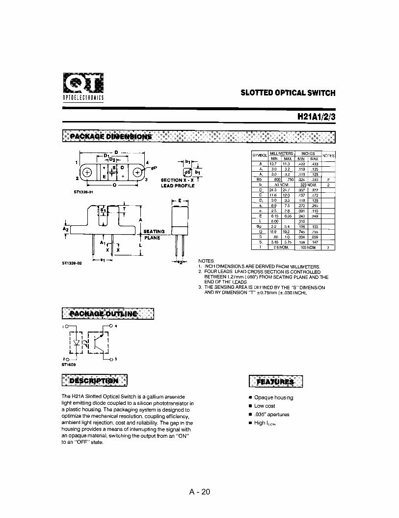
ULN2801A
ULN2804A - ULN2805AULN2802A - ULN2803A
September 1997
EIGHT DARLINGTON ARRAYS
.EIGHTDARLINGTONS WITHCOMMON EMIT-TERS.OUTPUT CURRENT TO 500 mA.OUTPUT VOLTAGE TO 50 V. INTEGRAL SUPPRESSION DIODES.VERSIONS FOR ALL POPULAR LOGIC FAMI-LIES.OUTPUT CAN BE PARALLELED. INPUTS PINNED OPPOSITE OUTPUTS TOSIMPLIFY BOARD LAYOUT
DESCRIPTION
The ULN2801A-ULN2805Aeach contain eight dar-lington transistors with common emitters and inte-gral suppression diodes for inductive loads. Eachdarlington features a peak load current rating of600mA (500mA continuous) and can withstand atleast50V in the off state.Outputsmay be paralleledfor higher current capability.Five versions are available to simplify interfacing tostandard logic families : the ULN2801A is designedfor generalpurpose applicationswith a current limitresistor ; the ULN2802Ahas a 10.5kΩ input resistorand zener for 14-25V PMOS; the ULN2803Ahas a2.7kΩ input resistor for 5V TTL and CMOS ; theULN2804A has a 10.5kΩ input resistor for 6-15VCMOS and the ULN2805A is designed to sink aminimum of 350mA for standard and Schottky TTLwhere higher output current is required.All types are supplied in a 18-lead plastic DIP witha copperlead fromandfeaturethe convenientinput-opposite-outputpinout to simplify board layout.
DIP18
PIN CONNECTION (top view)8
A - 10

SCHEMATIC DIAGRAM AND ORDER CODES
For ULN2801A (each driver for PMOS-CMOS) For ULN2802A (each driver for 14-15 V PMOS)
For ULN2804A (each driver for 6-15 VCMOS/PMOS
For ULN2803A (each driver for 5 V, TTL/CMOS)
For ULN2805A (each driver for high out TTL)
ULN2801A - ULN2802A - ULN2803A - ULN2804A - ULN2805A
A - 11

THERMAL DATA
Symbol Parameter Value Unit
Rth j–amb Thermal Resistance Junction-ambient Max. 55 °C/W
ELECTRICAL CHARACTERISTICS (Tamb = 25oC unless otherwise specified)
Symbol Parameter Test Conditions Min. Typ. Max. Unit Fig.ICEX Output Leakage Current VCE = 50V
Tamb = 70°C, VCE = 50VTamb = 70°Cfor ULN2802A
VCE = 50V, Vi = 6Vfor ULN2804A
VCE = 50V, Vi = 1V
50100
500
500
µAµA
µA
µA
1a1a
1b
1b
VCE(sat) Collector-emitterSaturation Voltage
IC = 100mA, IB = 250µAIC = 200mA, IB = 350µAIC = 350mA, IB = 500µA
0.91.11.3
1.11.31.6
VVV
2
Ii(on) Input Current for ULN2802A Vi = 17Vfor ULN2803A Vi = 3.85Vfor ULN2804A Vi = 5V
Vi = 12Vfor ULN2805A Vi = 3V
0.820.930.35
11.5
1.251.350.51.452.4
mAmAmAmAmA
3
Ii(off) Input Current Tamb = 70°C, IC = 500µA 50 65 µA 4Vi(on) Input Voltage VCE = 2 V
for ULN2802AIC = 300mA
for ULN2803AIC = 200mAIC = 250mAIC = 300mA
for ULN2804AIC = 125mAIC = 200mAIC = 275mAIC = 350mA
for ULN2805AIC = 350mA
13
2.42.73
5678
2.4
V
VVV
VVVV
V
5
hFE DC Forward Current Gain for ULN2801AVCE = 2V, IC = 350mA 1000 – 2
Ci Input Capacitance 15 25 pF –tPLH Turn-on Delay Time 0.5 Vi to 0.5 Vo 0.25 1 µs –
tPHL Turn-off Delay Time 0.5 Vi to 0.5 Vo 0.25 1 µs –IR Clamp Diode Leakage Current VR = 50V
Tamb = 70°C, VR = 50V50
100µAµA
66
VF Clamp Diode Forward Voltage IF = 350mA 1.7 2 V 7
ABSOLUTE MAXIMUM RATINGS
Symbol Parameter Value UnitVo Output Voltage 50 V
Vi Input Voltagefor ULN2802A, UL2803A, ULN2804Afor ULN2805A
3015
V
IC Continuous Collector Current 500 mAIB Continuous Base Current 25 mA
Ptot Power Dissipation(one Darlington pair)(total package)
1.02.25
W
Tamb Operating Ambient Temperature Range – 20 to 85 °C
Tstg Storage Temperature Range – 55 to 150 °CTj Junction Temperature Range – 20 to 150 °C
ULN2801A - ULN2802A - ULN2803A - ULN2804A - ULN2805A 8
A - 12

TEST CIRCUITS
Figure 1a. Figure 1b.
Figure 2. Figure 3.
Figure 4. Figure 5.
Figure 6. Figure 7.
ULN2801A - ULN2802A - ULN2803A - ULN2804A - ULN2805A
A - 13

Figure 8 : Collector Current as a Function ofSaturationVoltage.
Figure 9 : Collector Current as a FunctionofInputCurrent.
Figure 10 : Allowable Average Power Dissipationas a Functionof Ambient Temperature.
Figure 11 : Peak Collector Current as a Functionof Duty Cycle.
Figure 12 : Peak Collector Current as a Functionof Duty.
Figure 13 : InputCurrent as a Function of InputVoltage(for ULN2802A).
ULN2801A - ULN2802A - ULN2803A - ULN2804A - ULN2805A /8
A - 14

Figure 14 : InputCurrent as a Function of InputVoltage (for ULN2804A)
Figure 15 : InputCurrent as a Function of InputVoltage (for ULN2803A)
Figure 16 : InputCurrent as a Function of InputVoltage (for ULN2805A)
ULN2801A - ULN2802A - ULN2803A - ULN2804A - ULN2805
A- 15

DIP18 PACKAGE MECHANICAL DATA
DIM.mm inch
MIN. TYP. MAX. MIN. TYP. MAX.
a1 0.254 0.010
B 1.39 1.65 0.055 0.065
b 0.46 0.018
b1 0.25 0.010
D 23.24 0.915
E 8.5 0.335
e 2.54 0.100
e3 20.32 0.800
F 7.1 0.280
I 3.93 0.155
L 3.3 0.130
Z 1.27 1.59 0.050 0.063
ULN2801A - ULN2802A - ULN2803A - ULN2804A - ULN2805A 8
A - 16

CMPS03 - Robot Compass Module This compass module has been specifically designed for use in robots as an aid to navigation. The aim was to produce a unique number to represent the direction the robot is facing. The compass uses the Philips KMZ51 magnetic field sensor, which is sensitive enough to detect the Earths magnetic field. The output from two of them mounted at right angles to each other is used to compute the direction of the horizontal component of the Earths magnetic field. Connections to the compass module The compass module requires a 5v power supply at a nominal 15mA. There are two ways of getting the bearing from the module. A PWM signal is available on pin 4, or an I2C interface is provided on pins 2,3. The PWM signal is a pulse width modulated signal with the positive width of the pulse representing the angle. The pulse width varies from 1mS (0° ) to 36.99mS (359.9 ° ) – in other words 100uS/° with a +1mS offset. The signal goes low for 65mS between pulses, so the cycle time is 65mS + the pulse width - i.e. 66ms-102ms. The pulse is generated by a 16 bit timer in the processor giving a 1uS resolution, however I would not recommend measuring this to anything better than 0.1° (10uS). Make sure you connect the I2C pins, SCL and SDA, to the 5v supply if you are using the PWM, as there are no pull-up resistors on these pins. Pin 2,3 are an I2C interface and can be used to get a direct readout of the bearing. If the I2C interface is not used then these pins should be pulled high (to +5v) via a couple of resistors. Around 47k is ok, the values are not at all critical.
A - 17

I2C communication protocol with the compass module is the same as popular eeprom's such as the 24C04.. First send a start bit, the module address (0XC0) with the read/write bit low, then the register number you wish to read. This is followed by a repeated start and the module address again with the read/write bit high (0XC1). You now read one or two bytes for 8bit or 16bit registers respectively. 16bit registers are read high byte first. The compass has a 16 byte array of registers, some of which double up as 16 bit registers as follows;
Register Function 0 Software Revision Number 1 Compass Bearing as a byte, i.e. 0-255 for a full circle
2,3 Compass Bearing as a word, i.e. 0-3599 for a full circle, representing 0-359.9 degrees.
4,5 Internal Test - Sensor1 difference signal - 16 bit signed word 6,7 Internal Test - Sensor2 difference signal - 16 bit signed word 8,9 Internal Test - Calibration value 1 - 16 bit signed word
10,11 Internal Test - Calibration value 2 - 16 bit signed word 12 Unused - Read as Zero 13 Unused - Read as Zero 14 Unused - Read as Undefined 15 Calibrate Command - Write 255 to perform calibration step. See text.
Register 0 is the Software revision number (8 at the time of writing). Register 1 is the bearing converted to a 0-255 value. This may be easier for some applications than 0-360 which requires two bytes. For those who require better resolution registers 2 and 3 (high byte first) are a 16 bit unsigned integer in the range 0-3599. This represents 0-359.9°. Registers 4 to 11 are internal test registers and 12,13 are unused. Register 14 is undefined. Don't read them if you don't want them - you'll just waste your I2C bandwidth. Register 15 is used to calibrate the compass.
A - 18
The I2C interface does not have any pull-up resistors on the board, these should be provided elsewhere, most probably with the bus master. They are required on both the SCL and SDA lines, but only once for the whole bus, not on each module. I suggest a value of 1k8 if you are going to be working up to 400KHz and 1k2 or even 1k if you are going up to 1MHz. The compass is designed to work at up to the standard clock speed (SCL) of 100KHz, however the clock speed can be raised to 1MHZ providing the following precaution is taken; At speeds above around 160KHz the CPU cannot respond fast enough to read the I2C data. Therefore a small delay of 50uS should be inserted either side of writing the register address. No delays are required anywhere else in the sequence. By doing this, I have tested the compass module up to 1.3MHz SCL clock speed. The compass module always operates as a slave, its never a bus master. Pin 7 is an input pin selecting either 50Hz (low) or 60Hz (high) operation. I added this option after noticing a jitter of around 1.5° in the output. The cause was the 50Hz mains field in my workshop. By converting in synchronism with the mains frequency this was reduced to around 0.2° . An internal conversion is done every 40mS (50Hz) or every 33.3mS (60Hz). The pin has an on-board pull-up can be left unconnected for 60Hz operation. There is no synchronism between the PWM or I2C outputs and the conversion. They both retrieve the most recent internal reading, which is continuously converted, whether it is used or not. Pin 6 is us ed to calibrate the compass. The calibrate input (pin 6) has an on-board pull-up resistor and can be left unconnected after calibration. Pins 5 and 8 are No Connect. Actually pin 8 is the processor reset line and has an on-board pull-up resistor. It is there so that we can program the processor chip after placement on the PCB. PCB Drilling Plan The following diagram shows the CMPS03 PCB mounting hole positions.
A - 19
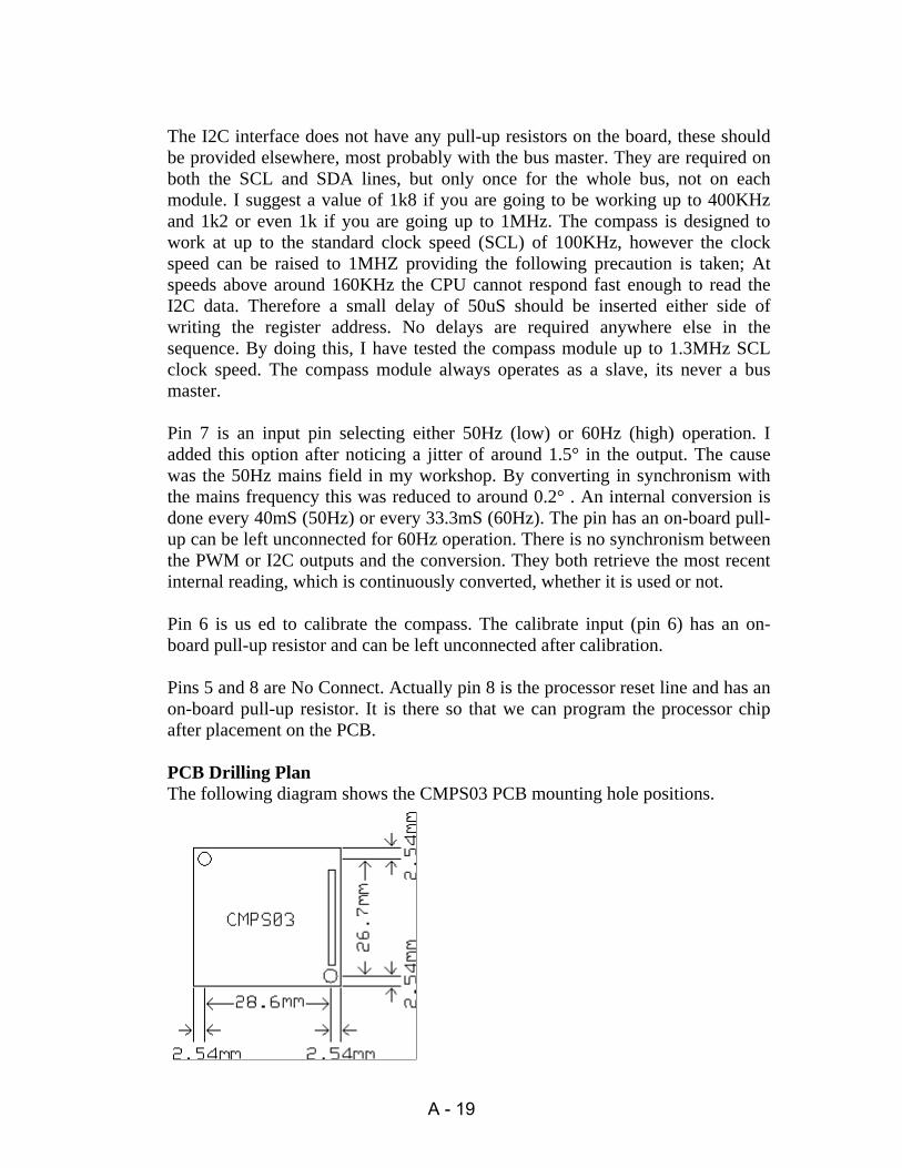
A - 20

A - 21

A - 22

A - 23

The Extended Concise LCD Data Sheet for HD44780
Version: 25.6.1999
Instruction RS RW D7 D6 D5 D4 D3 D2 D1 D0 Description Clock-Cycles
NOP 0 0 0 0 0 0 0 0 0 0 No Operation 0
Clear Display 0 0 0 0 0 0 0 0 0 1 Clear display & set address counter to zero 165
Cursor Home 0 0 0 0 0 0 0 0 1 xSet adress counter to zero, return shifteddisplay to original position.DD RAM contents remains unchanged.
3
Entry ModeSet
0 0 0 0 0 0 0 1 I/D S Set cursor move direction (I/D) and specifyautomatic display shift (S).
3
DisplayControl
0 0 0 0 0 0 1 D C B Turn display (D), cursor on/off (C), andcursor blinking (B).
3
Cursor /Display shift
0 0 0 0 0 1 S/C R/L x x Shift display or move cursor (S/C) andspecify direction (R/L).
3
Function Set 0 0 0 0 1 DL N F x x Set interface data width (DL), number ofdisplay lines (N) and character font (F).
3
Set CGRAMAddress
0 0 0 1 CGRAM Address Set CGRAM address. CGRAM data is sentafterwards.
3
Set DDRAMAddress
0 0 1 DDRAM Address Set DDRAM address. DDRAM data is sentafterwards.
3
Busy Flag &Address
0 1 BF Address Counter Read busy flag (BF) and address counter 0
Write Data 1 0 Data Write data into DDRAM or CGRAM 3
Read Data 1 1 Data Read data from DDRAM or CGRAM 3
I/D 10
IncrementDecrement
R/L 10
Shift to the rightShift to the left
S 10
Automatic display shift DL 10
8 bit interface4 bit interface
D 10
Display ONDisplay OFF
N 10
2 lines1 line
C 10
Cursor ONCursor OFF
F 10
5x10 dots5x7 dots
B 10
Cursor blinking
x : Don't care
S/C 10
Display shiftCursor move
DDRAM : Display Data RAM
CGRAM : Character Generator RAM
LCD Display with 2 lines x 40 characters :
LCD Display with 2 lines x 16 characters :Pin No Name Function Description
1 Vss Power GND2 Vdd Power + 5 V3 Vee Contrast Adj. (-2) 0 - 5 V4 RS Command Register Select5 R/W Command Read / Write6 E Command Enable (Strobe)7 D0 I/O Data LSB8 D1 I/O Data9 D2 I/O Data10 D3 I/O Data11 D4 I/O Data12 D5 I/O Data13 D6 I/O Data14 D7 I/O Data MSB
A - 24

Bus Timing Characteristics( Ta = - 20 to + 75°C )
Write-Cycle VDD 2.7 - 4.5 V (2) 4.5 - 5.5 V (2) 2.7 - 4.5 V (2) 4.5 - 5.5 V (2)
Parameter Symbol Min(1) Typ(1) Max(1) Unit
Enable Cycle Time tc 1000 500 - - - ns
Enable Pulse Width (High) tw 450 230 - - - ns
Enable Rise/Fall Time tr, tf - - - 25 20 ns
Address Setup Time tas 60 40 - - - ns
Address Hold Time tah 20 10 - - - ns
Data Setup Time tds 195 80 - - - ns
Data Hold Time th 10 10 - - - ns
(1) The above specifications are indications only (based on Hitachi HD44780). Timing will vary from manufacturerto manufacturer.
(2) Power Supply : HD44780 S : VDD = 4.5 - 5.5 V HD44780 U : VDD = 2.7 - 5.5 V
This data sheet refers to specifications for the Hitachi HD44780 LCD Driver chip, which is used for most LCDmodules.
Common types are : 1 line x 20 characters2 lines x 16 characters2 lines x 20 characters2 lines x 40 characters4 lines x 20 characters4 lines x 40 characters
© 1998/1999 by Craig Peacock, Australia http://www.beyondlogic.orgPeter Luethi, Switzerland http://www.electronic-engineering.ch
A - 25

LAMPIRAN B
PERANGKAT LUNAK

;----------------------------------------------------- ;PROGRAM UTAMA PENGENDALI ;PROTOTIPE MOBIL ;BY: RIKIAN CHANDRAWAN DS ;----------------------------------------------------- ;INISIALISASI REGISTER DAN ;ALAMAT $MOD52 OPTOCOUPLER EQU P3.5 ;(TIMER1) KEYPAD EQU P1 ;=============================== ;ALAMAT UNTUK MEMORI SUDUT ;=============================== DATA_SUDUT_LOW EQU 35H DATA_SUDUT_HIGH EQU 34H S_SATUAN EQU 33H S_PULUHAN EQU 32H S_RATUSAN EQU 31H ;=============================== ;=============================== ;ALAMAT UNTUK MEMORI JARAK ;=============================== DATA_JARAK_HIGH EQU 3AH DATA_JARAK_LOW EQU 39H J_SATUAN EQU 38H J_PULUHAN EQU 37H J_RATUSAN EQU 36H ;=============================== PENGALI_PULUHAN EQU 0AH PENGALI_RATUSAN EQU 64H MILI_KE_MIKRO EQU 1000D KELILING EQU 0DH ;=============================== ; TENTANG MOTOR STEPPER ;=============================== STEPPER EQU P2 SKA1 EQU 00001001B SKA2 EQU 00001000B SKA3 EQU 00001100B SKA4 EQU 00000100B SKA5 EQU 00000110B SKA6 EQU 00000010B SKA7 EQU 00000011B SKA8 EQU 00000001B ;SISI KIRI SKI1 EQU 10010000B SKI2 EQU 10000000B SKI3 EQU 11000000B SKI4 EQU 01000000B SKI5 EQU 01100000B SKI6 EQU 00100000B SKI7 EQU 00110000B SKI8 EQU 00010000B
;=============================== ;=============================== ;TENTANG LCD ;=============================== LCD EQU P0 LCD_FUNC_SET EQU 00111000B LCD_CLEAR EQU 00000001B LCD_TAMPILKAN_CTRL EQU 00001111B LCD_LINE1 EQU 10000000B LCD_LINE2 EQU 11000000B LCD_LINE1_9 EQU 10001000B LCD_LINE2_9 EQU 11001000B LCD_DRJT EQU 10001011B LCD_CM EQU 11001011B ENABLE EQU P3.0 RW EQU P3.1 RS EQU P3.2 ;=============================== ORG 0000H LJMP START ORG 50H START: MOV P0,#0H MOV P1,#0H MOV P2,#0H MOV P3,#0H ACALL INISIALISASI_PEMBUAT ;MENAMPILKAN NAMA PEMBUAT START1: ACALL LCD_DIBERSIHKAN ACALL DIS_SUDUT ACALL DIS_JARAK SUDUT1: ACALL DIS_SUDUT MOV R0,#31H ACALL AMBIL_SUDUT JARAK1: ACALL DIS_JARAK MOV R0,#36H ACALL AMBIL_JARAK ACALL BELOK START2: CLR TR2 ACALL MAJU START3: ACALL LCD_DIBERSIHKAN ACALL OPTION ;UNTUK ULANG LAGI ATAU TIDAK LJMP SELESAI
B- 1

;----------------------------------------------------- ; TAMPILAN SUDUT DAN JARAK ;----------------------------------------------------- DIS_SUDUT: MOV A,#80H ACALL PERINTAH MOV A,#'I' ;I ACALL TAMPILKAN MOV A,#'N' ;N ACALL TAMPILKAN MOV A,#'P' ;P ACALL TAMPILKAN MOV A,#20H ;SPASI ACALL TAMPILKAN MOV A,#'S' ;S ACALL TAMPILKAN MOV A,#'D' ;D ACALL TAMPILKAN MOV A,#'T' ;T ACALL TAMPILKAN MOV A,#3AH ;: ACALL TAMPILKAN MOV A,#LCD_DRJT ACALL PERINTAH MOV A,#0DFH ;DERAJAT ACALL TAMPILKAN RET DIS_JARAK: MOV A,#0C0H ACALL PERINTAH MOV A,#'I' ;I ACALL TAMPILKAN MOV A,#'N' ;N ACALL TAMPILKAN MOV A,#'P' ;P ACALL TAMPILKAN MOV A,#20H ;SPASI ACALL TAMPILKAN MOV A,#'J' ;J ACALL TAMPILKAN MOV A,#'R' ;R ACALL TAMPILKAN MOV A,#'K' ;K ACALL TAMPILKAN MOV A,#3AH ;: ACALL TAMPILKAN MOV A,#LCD_CM ACALL PERINTAH MOV A,#43H ;C ACALL TAMPILKAN MOV A,#4DH ;M ACALL TAMPILKAN RET
;----------------------------------------------------- ; PROGRAM UNTUK ;MENGAMBIL MASUKAN SUDUT DAN ; JARAK ;----------------------------------------------------- AMBIL_SUDUT: MOV A,#LCD_LINE1_9 ACALL PERINTAH ACALL CEK_KEYPAD CJNE A,#0E5H,SUDUT_BENAR LJMP SUDUT1 SUDUT_BENAR: MOV A,S_PULUHAN MOV B,#PENGALI_PULUHAN MUL AB MOV B,S_SATUAN ADD A,B ADD A,#0AH ;supaya sama dengan kompas MOV R1,A ;BYTE RENDAH MOV A,S_RATUSAN MOV B,#PENGALI_RATUSAN MUL AB CLR C ADD A,R1 MOV DATA_SUDUT_LOW,A MOV A,B ADDC A,#00H MOV DATA_SUDUT_HIGH,A MOV A,S_RATUSAN CJNE A,#0H,CEK1 SJMP TAMBAH1 CEK1: CJNE A,#01H,CEK2 SJMP TAMBAH1 CEK2: CJNE A,#02H,CEK3 SJMP TAMBAH2 CEK3: CJNE A,#03H,TETAP MOV B,#64H MOV A,DATA_SUDUT_LOW MUL AB MOV DATA_SUDUT_LOW,A MOV A,#64H ADD A,B MOV DATA_SUDUT_HIGH,A SJMP TETAP TAMBAH1: MOV B,#64H MOV A,DATA_SUDUT_LOW MUL AB
B- 2

MOV DATA_SUDUT_LOW,A MOV DATA_SUDUT_HIGH,B SJMP TETAP TAMBAH2: MOV B,#64H MOV A,DATA_SUDUT_LOW MUL AB MOV DATA_SUDUT_LOW,A MOV DATA_SUDUT_HIGH,B
MOV A,DATA_SUDUT_HIGH CJNE A,#01H,TETAP MOV B,#64H ADD A,B MOV DATA_SUDUT_HIGH,A TETAP:
MOV A,DATA_SUDUT_LOW CLR C ADD A,#7EH MOV DATA_SUDUT_LOW,A MOV A,DATA_SUDUT_HIGH ADDC A,#04H MOV DATA_SUDUT_HIGH,A RET AMBIL_JARAK: MOV A,#LCD_LINE2_9 ACALL PERINTAH ACALL CEK_KEYPAD CJNE A,#0E5H,JARAK_BENAR MOV A,#LCD_LINE1_9 LJMP JARAK1 JARAK_BENAR: MOV A,J_PULUHAN MOV B,#PENGALI_PULUHAN MUL AB MOV B,J_SATUAN ADD A,B MOV A,R1 MOV A,J_RATUSAN MOV B,#PENGALI_RATUSAN MUL AB CLR C ADD A,R1 MOV DATA_JARAK_LOW,A MOV A,B ADDC A,#00H MOV DATA_JARAK_HIGH,A RET ;----------------------------------------------------- ; PROGRAM UNTUK ;MENGAMBIL MASUKKAN DARI ; KEYPAD ;----------------------------------------------------
CEK_KEYPAD: MOV 2FH,#03H CEK_DATA: MOV KEYPAD,#7FH ;KIRIM DATA MOV A,KEYPAD ANL A,#0FDH TOMBOL1: CJNE A,#7CH,TOMBOL2 ACALL DELAY_KEYPAD MOV A,#01H ACALL TAMPILKAN_KEYPAD AJMP MEMASUKKAN_DATA TOMBOL2: CJNE A,#79H,TOMBOL3 ACALL DELAY_KEYPAD MOV A,#02H ACALL TAMPILKAN_KEYPAD AJMP MEMASUKKAN_DATA TOMBOL3: CJNE A,#75H,TOMBOL4 ACALL DELAY_KEYPAD MOV A,#03H ACALL TAMPILKAN_KEYPAD AJMP MEMASUKKAN_DATA TOMBOL4: MOV KEYPAD,#0BFH ;KIRIM DATA MOV A,KEYPAD ANL A,#0FDH CJNE A,#0BCH,TOMBOL5 ACALL DELAY_KEYPAD MOV A,#04H ACALL TAMPILKAN_KEYPAD AJMP MEMASUKKAN_DATA TOMBOL5: CJNE A,#0B9H,TOMBOL6 ACALL DELAY_KEYPAD MOV A,#05H ACALL TAMPILKAN_KEYPAD AJMP MEMASUKKAN_DATA TOMBOL6: CJNE A,#0B5H,TOMBOL7 ACALL DELAY_KEYPAD MOV A,#06H ACALL TAMPILKAN_KEYPAD AJMP MEMASUKKAN_DATA TOMBOL7:
B- 3
MOV KEYPAD,#0DFH ;KIRIM DATA MOV A,KEYPAD ANL A,#0FDH CJNE A,#0DCH,TOMBOL8 ACALL DELAY_KEYPAD MOV A,#07H ACALL TAMPILKAN_KEYPAD AJMP MEMASUKKAN_DATA TOMBOL8: CJNE A,#0D9H,TOMBOL9 ACALL DELAY_KEYPAD MOV A,#08H ACALL TAMPILKAN_KEYPAD AJMP MEMASUKKAN_DATA TOMBOL9: CJNE A,#0D5H,TOMBOL_BINTANG ACALL DELAY_KEYPAD MOV A,#09H ACALL TAMPILKAN_KEYPAD AJMP MEMASUKKAN_DATA TOMBOL_BINTANG: MOV KEYPAD,#0EFH ;KIRIM DATA MOV A,KEYPAD ANL A,#0FDH CJNE A,#0ECH,TOMBOL0 ACALL DELAY_KEYPAD AJMP MASUKKAN_DATA_OK TOMBOL0: CJNE A,#0E9H,TOMBOL_PAGAR ACALL DELAY_KEYPAD MOV A,#00H ACALL TAMPILKAN_KEYPAD AJMP MEMASUKKAN_DATA TOMBOL_PAGAR: CJNE A,#0E5H,KEMBALI ACALL DELAY_KEYPAD AJMP SALAH KEMBALI: AJMP CEK_DATA MEMASUKKAN_DATA: MOV @R0,A INC R0 DEC 2FH LJMP CEK_DATA
MASUKKAN_DATA_OK: RET SALAH: RET ;----------------------------------------------------- ; PROGRAM YANG ;BERHUBUNGAN DENGAN LCD ;----------------------------------------------------- INISIALISASI_PEMBUAT: MOV A,#3CH ACALL PERINTAH MOV A,#0FH ACALL PERINTAH MOV A,#06H ACALL PERINTAH MOV A,#LCD_CLEAR ACALL PERINTAH MOV A,#80H ACALL PERINTAH MOV A,#'R' ;R ACALL TAMPILKAN MOV A,#'I' ;I ACALL TAMPILKAN MOV A,#'K' ;K ACALL TAMPILKAN MOV A,#'I' ;I ACALL TAMPILKAN MOV A,#20h ACALL TAMPILKAN MOV A,#'0' ;0 ACALL TAMPILKAN MOV A,#'1' ;1 ACALL TAMPILKAN MOV A,#'2' ;2 ACALL TAMPILKAN MOV A,#'2' ;2 ACALL TAMPILKAN MOV A,#'0' ;0 ACALL TAMPILKAN MOV A,#'2' ;2 ACALL TAMPILKAN MOV A,#'0' ;0 ACALL TAMPILKAN MOV A,#0C0h ACALL PERINTAH MOV A,#'0' ;0 ACALL TAMPILKAN MOV A,#'-' ;- ACALL TAMPILKAN MOV A,#00100111B ;' ACALL TAMPILKAN MOV A,#'=' ;= ACALL TAMPILKAN MOV A,#'0' ;0 ACALL TAMPILKAN
B- 4

MOV A,#20H ACALL TAMPILKAN MOV A,#'C' ;C ACALL TAMPILKAN MOV A,#'M' ;M ACALL TAMPILKAN MOV A,#'P' ;P ACALL TAMPILKAN MOV A,#'S' ;S ACALL TAMPILKAN MOV A,#'-' ;- ACALL TAMPILKAN MOV A,#'0' ;0 ACALL TAMPILKAN MOV A,#'3' ;3 ACALL TAMPILKAN ACALL DELAY_PEMBUAT RET PERINTAH: ACALL CEK_BUSY MOV LCD,A CLR RS CLR RW SETB ENABLE CLR ENABLE RET TAMPILKAN_KEYPAD: ADD A,#30H TAMPILKAN: ACALL CEK_BUSY MOV LCD,A SETB RS CLR RW SETB ENABLE CLR ENABLE RET CEK_BUSY: CLR ENABLE MOV LCD,#0FFH CLR RS SETB RW TUNGGU: CLR ENABLE SETB ENABLE JB P0.7,TUNGGU CLR ENABLE RET LCD_DIBERSIHKAN: MOV A,#LCD_CLEAR ACALL PERINTAH RET
LCD_OPTION: MOV A,#80H ACALL PERINTAH MOV A,#43H ;C ACALL TAMPILKAN MOV A,#4FH ;O ACALL TAMPILKAN MOV A,#42H ;B ACALL TAMPILKAN MOV A,#41H ;A ACALL TAMPILKAN MOV A,#20H ;SPASI ACALL TAMPILKAN MOV A,#4CH ;L ACALL TAMPILKAN MOV A,#41H ;A ACALL TAMPILKAN MOV A,#47H ;G ACALL TAMPILKAN MOV A,#49H ;I ACALL TAMPILKAN MOV A,#3FH ;? ACALL TAMPILKAN MOV A,#0C0H ;BARIS2 ACALL PERINTAH MOV A,#59H ;Y ACALL TAMPILKAN MOV A,#45H ;E ACALL TAMPILKAN MOV A,#53H ;S ACALL TAMPILKAN MOV A,#20H ;SPASI ACALL TAMPILKAN MOV A,#2FH ;/ ACALL TAMPILKAN MOV A,#20H ;SPASI ACALL TAMPILKAN MOV A,#4EH ;N ACALL TAMPILKAN MOV A,#4FH ;O ACALL TAMPILKAN RET ;----------------------------------------------------- ; PROGRAM UNTUK ;MENGAMBIL PWM DARI CMPS-03 ;----------------------------------------------------- COMPASS: MOV TL2,#00H MOV TH2,#00H JNB P1.1,$ SETB TR2 JNB EXF2,$ CLR EXF2 CLR TR2
B- 5
CLR C MOV A,RCAP2L ADD A,#7EH MOV B,A MOV A,RCAP2H ADDC A,#04H MOV R3,A MOV A,B CJNE A,DATA_SUDUT_LOW,TERUS MOV A,R3 CJNE A,DATA_SUDUT_HIGH,TERUS CLR EXF2 CLR TR2 LJMP START2 TERUS: RET ;----------------------------------------------------- ;PROGRAM UNTUK MENGATUR ARAH ; BELOK DARI MOTOR STEPPER ;----------------------------------------------------- BELOK: MOV T2MOD,#00000001B MOV T2CON,#00001001B ;MODE CAPTURE SETB ET2 SETB TR2 MOV R3,#03H SAFETY1: ;UNTUK MENGETAHUI BAHWA DATA ;DARI TIMER 2 BENAR MOV TL2,#00H MOV TH2,#00H JNB P1.1,$ SETB TR2 JNB EXF2,$ CLR EXF2 CLR TR2 DJNZ R3,SAFETY1 MOV A,RCAP2H ADD A,#04H MOV R4,A MOV A,DATA_SUDUT_HIGH CLR C SUBB A,R4 JNC KANAN KIRI: MOV A,#SKI8 MOV R2,#SKA1 ORL A,R2 MOV P2,A ACALL DELAY_STEPPER ACALL COMPASS
MOV A,#SKI7 MOV R2,#SKA2 ORL A,R2 MOV P2,A ACALL DELAY_STEPPER ACALL COMPASS MOV A,#SKI6 MOV R2,#SKA3 ORL A,R2 MOV P2,A ACALL DELAY_STEPPER ACALL COMPASS MOV A,#SKI5 MOV R2,#SKA4 ORL A,R2 MOV P2,A ACALL DELAY_STEPPER ACALL COMPASS MOV A,#SKI4 MOV R2,#SKA5 ORL A,R2 MOV P2,A ACALL DELAY_STEPPER ACALL COMPASS MOV A,#SKI3 MOV R2,#SKA6 ORL A,R2 MOV P2,A ACALL DELAY_STEPPER ACALL COMPASS MOV A,#SKI2 MOV R2,#SKA7 ORL A,R2 MOV P2,A ACALL DELAY_STEPPER ACALL COMPASS MOV A,#SKI1 MOV R2,#SKA8 ORL A,R2 MOV P2,A ACALL DELAY_STEPPER ACALL COMPASS LJMP KIRI KANAN: MOV A,#SKI1 MOV R2,#SKA8 ORL A,R2 MOV P2,A ACALL DELAY_STEPPER ACALL COMPASS
B- 6

MOV A,#SKI2 MOV R2,#SKA7 ORL A,R2 MOV P2,A ACALL DELAY_STEPPER ACALL COMPASS MOV A,#SKI3 MOV R2,#SKA6 ORL A,R2 MOV P2,A ACALL DELAY_STEPPER ACALL COMPASS MOV A,#SKI4 MOV R2,#SKA5 ORL A,R2 MOV P2,A ACALL DELAY_STEPPER ACALL COMPASS MOV A,#SKI5 MOV R2,#SKA4 ORL A,R2 MOV P2,A ACALL DELAY_STEPPER ACALL COMPASS MOV A,#SKI6 MOV R2,#SKA3 ORL A,R2 MOV P2,A ACALL DELAY_STEPPER ACALL COMPASS MOV A,#SKI7 MOV R2,#SKA2 ORL A,R2 MOV P2,A ACALL DELAY_STEPPER ACALL COMPASS MOV A,#SKI8 MOV R2,#SKA1 ORL A,R2 MOV P2,A ACALL DELAY_STEPPER ACALL COMPASS LJMP KANAN MAJU: MOV TMOD,#01010000B ;PAKAI TIMER1 SETB TR1 MAJU1: MOV A,#SKI1
MOV R2,#SKA1 ORL A,R2 MOV P2,A ACALL DELAY_STEPPER ACALL JALAN MOV A,#SKI2 MOV R2,#SKA2 ORL A,R2 MOV P2,A ACALL DELAY_STEPPER ACALL JALAN MOV A,#SKI3 MOV R2,#SKA3 ORL A,R2 MOV P2,A ACALL DELAY_STEPPER ACALL JALAN MOV A,#SKI4 MOV R2,#SKA4 ORL A,R2 MOV P2,A ACALL DELAY_STEPPER ACALL JALAN MOV A,#SKI5 MOV R2,#SKA5 ORL A,R2 MOV P2,A ACALL DELAY_STEPPER ACALL JALAN MOV A,#SKI6 MOV R2,#SKA6 ORL A,R2 MOV P2,A ACALL DELAY_STEPPER ACALL JALAN MOV A,#SKI7 MOV R2,#SKA7 ORL A,R2 MOV P2,A ACALL DELAY_STEPPER ACALL JALAN MOV A,#SKI8 MOV R2,#SKA8 ORL A,R2 MOV P2,A ACALL DELAY_STEPPER ACALL JALAN LJMP MAJU1
B- 7

;----------------------------------------------------- ; PROGRAM UNTUK MENGETAHUI JARAK ; DENGAN MENGGUNAKAN OPTOCOPLER ;----------------------------------------------------- JALAN: MOV A,TL1 CJNE A,DATA_JARAK_LOW,TERUS1 MOV A,TH1 CJNE A,DATA_JARAK_HIGH,TERUS1 CLR TR1 LJMP START3 TERUS1: RET ;----------------------------------------------------- ; DELAY-DELAY ;----------------------------------------------------- DELAY_PEMBUAT: MOV R5,#18H DELAY_PEMBUAT1: MOV R6,#0F9H DELAY_PEMBUAT2: MOV R7,#0FBH DELAY_PEMBUAT3: DJNZ R7,DELAY_PEMBUAT3 DJNZ R6,DELAY_PEMBUAT2 DJNZ R5,DELAY_PEMBUAT1 RET DELAY_STEPPER: MOV R5,#01AH DELAY_STEPPER2: MOV R4,#0FFH DELAY_STEPPER1: DJNZ R4,DELAY_STEPPER1 DJNZ R5,DELAY_STEPPER2 RET DELAY_KEYPAD: MOV R5,#02H DELAY_KEYPAD1: MOV R6,#0EAH DELAY_KEYPAD2: MOV R7,#0FAH DELAY_KEYPAD3: DJNZ R7,DELAY_KEYPAD3 DJNZ R6,DELAY_KEYPAD2 DJNZ R5,DELAY_KEYPAD1 RET
;------------------------------------------------- ; OPTION ;------------------------------------------------- OPTION: ACALL LCD_OPTION CHECK:
ACALL CEK_KEYPAD CJNE A,#0ECH,OPTION_NO LJMP START1 OPTION_NO: CJNE A,#0E5H,CHECK ACALL LCD_DIBERSIHKAN MOV A,#02H ACALL PERINTAH MOV A,#'T' ;T ACALL TAMPILKAN MOV A,#'E' ;E ACALL TAMPILKAN MOV A,#'R' ;R ACALL TAMPILKAN MOV A,#'I' ;I ACALL TAMPILKAN MOV A,#'M' ;M ACALL TAMPILKAN MOV A,#'A' ;A ACALL TAMPILKAN MOV A,#20H ;SPASI ACALL TAMPILKAN MOV A,#'K' ;K ACALL TAMPILKAN MOV A,#'A' ;A ACALL TAMPILKAN MOV A,#'S' ;S ACALL TAMPILKAN MOV A,#'I' ;I ACALL TAMPILKAN MOV A,#'H' ;H ACALL TAMPILKAN MOV A,#0C2H ACALL PERINTAH MOV A,#'B' ;B ACALL TAMPILKAN MOV A,#'y' ;y ACALL TAMPILKAN MOV A,#'e' ;e ACALL TAMPILKAN MOV A,#'-' ;- ACALL TAMPILKAN MOV A,#'B' ;B ACALL TAMPILKAN MOV A,#'y' ;y ACALL TAMPILKAN MOV A,#'e' ;e ACALL TAMPILKAN MOV A,#20H ;SPASI ACALL TAMPILKAN MOV A,#20H ;SPASI
B- 8

ACALL TAMPILKAN MOV A,#5EH ACALL TAMPILKAN MOV A,#5FH ACALL TAMPILKAN MOV A,#5EH ACALL TAMPILKAN SELESAI: END
B- 9

LAMPIRAN C
SKEMA RANGKAIAN

C - 1 C - 1
LAMPIRAN D
FOTO ALAT

D - 1 D - 1


