EEEB273 – Electronics Analysis & Design II Lecturer: Dr Jamaludin Bin Omar 10-1 Simplified BJT Simplified BJT Op Op-Amp Amp Circuit Circuit Reference: Neamen, Chapter 11 (10) Learning Outcome Able to: • Analyze a simplified BJT Op-amp circuit. 10.1) Simplified BJT Op-Amp Circuit • Figure 11.49 depicts a simple bipolar op-amp. Figure 11.49 10.1) Simplified BJT Op-Amp Circuit (Cont) • Simplified analysis and design only resistive loads are considered. • Diff-amp is biased with Widlar current source. • One-sided output of diff-amp is connected to Darlington pair gain stage. • Bypass capacitor C E is included to increase small- signal voltage gain. • Output stage is an emitter follower. • Generally, wanted the dc value of the output voltage v O = 0 when input voltage = 0 insert dc level shifting circuit between v O3 and v O . 10.2) DC Characteristics Example 11.15 Analyze the dc characteristics of BJT op-amp circuit. Neglect base currents. Assume V BE (on) = 0.7V for all transistors except Q 8 and Q 9 in Widlar. • Reference current I 1 : • Bias current I Q (from Widlar): I Q = 0.4 mA • Collector currents: I C1 = I C2 = I Q / 2 = 0.2 mA mA 1 3 . 19 ) 10 ( 7 . 0 10 1 = - - - = I = Q T Q I I V R I 1 2 ln 10. 2) DC Characteristics (Cont) • DC voltage at collector Q 2 V O2 = 10 -I C2 R C = 10 – (0.2m)(20k) V O2 = 6V = v cm (max) • Common-mode input range: -8.6V v cm 6V v cm (min) = -10 + V BE8 + V BE1 (ignoring I Q R 2 ) • Values for I R4 and I R5 : I R5 I R4 = 0.4 mA (neglecting base currents) mA 4 . 0 k 5 . 11 4 . 1 6 (on) 2 4 2 4 = - = - = R V V I BE O R
Able to: • Analyze a simplified BJT Op-amp circuit.
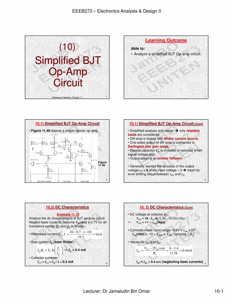
10.1) Simplified BJT Op-Amp Circuit
• Figure 11.49 depicts a simple bipolar op-amp.
Figure11.49
10.1) Simplified BJT Op-Amp Circuit (Cont)
• Simplified analysis and design only resistive loads are considered.• Diff-amp is biased with Widlar current source. • One-sided output of diff-amp is connected to Darlington pair gain stage.• Bypass capacitor CE is included to increase small-signal voltage gain.• Output stage is an emitter follower.
• Generally, wanted the dc value of the output voltage vO = 0 when input voltage = 0 insert dc level shifting circuit between vO3 and vO.
10.2) DC Characteristics
Example 11.15Analyze the dc characteristics of BJT op-amp circuit.Neglect base currents. Assume VBE(on) = 0.7V for all transistors except Q8 and Q9 in Widlar.
• Reference current I1:
• Bias current IQ (from Widlar):
IQ = 0.4 mA
• Collector currents: IC1 = IC2 = IQ / 2 = 0.2 mA
mA13.19
)10(7.0101 =−−−=I
=
QTQ I
IVRI 1
2 ln
10. 2) DC Characteristics (Cont)
• DC voltage at collector Q2VO2 = 10 - IC2 RC = 10 – (0.2m)(20k)
• DC voltage at collectors of Q3 and Q4VO3 = 10 – IR5 R5 = 10 – (0.4m)(5k)
VO3 = 8V is midway between 10V supply voltage and 6V dc input voltage (VO2) This allows a maximum symmetrical swing for time-varying vO3
• DC voltage level shifting by Q5 and R6:IR6 = IQ = 0.4 mA, since R3 = R2VB6 = VO3 – VBE(on) – IR6R6 = 8–0.7–(0.4m)(16.5k)
VB6 = 0.7 V produces a zero dc output at vO(emitter of Q6) for a zero diff-mode input voltage.
• Current IR7: mA2k5
10)10(
77 ==−−=
Rv
I OR
10. 3) AC Characteristics
Example 11.16Determine small-signal diff-mode voltage gain, AdUse Fig 11.49. Transistor parameters: = 100, VA = .
• Overall differential-mode gain:
Ad valid only if load resistance of following stages are considered in the calculation: Ri2: input resistance to Darlington pair. Ri3: input resistance to output stage.
−==
32
3
21
2321 ....
o
o
o
oodd v
vvv
vvv
AAAA
10. 3) AC Characteristics (Cont)
• One-sided diff-mode voltage gain of diff-amp:
Since load resistance Ri2 >> RC, there is no significant loading effect of 2nd stage on diff-amp.
( )
( )
8.751307k)||m/2)(20k70.7(
mA/V70.7)026.02/(m4.0)2/(
k1307)k5.6)(101(k6501
k650m4.0/)026.0()100(/
k5.6m4.0/)026.0)(100(/
2
1
432
24
23
44
22
1
==∴
=×==Ω=+=++=
Ω==≅
Ω===
=
=
d
TQm
i
RT
RT
iCm
d
od
A
VIg
rrR
IVr
IVr
RRg
vV
A
ππ
π
π
βββ
( )
( ) ( )[ ]
( ) ( ) 5.38k5)026.0(2
m4.02
M8.5211
k3.1m2/)026.0)(100(/
k5.6m4.0/)026.0)(100(/
2
54
2
76653
76
65
354
2
==≅∴
Ω=+++++=Ω===
Ω===
=
RV
IA
RrRrR
IVr
IVr
RRV
IA
T
R
i
RT
RT
iT
R
ββββ
ππ
π
π
10. 3) AC Characteristics (Cont)
• The voltage gain of the Darlington pair:
Since Ri3 >> R5, the output stage does not load down the gain stage, and small-signal voltage gain is approximately
291815.388.75..
1/
321
33
=××==
≅=
AAAA
vvA
dd
oo
10. 3) AC Characteristics (Cont)
• The combination of Q5 and Q6 forms an emitter follower, and the gain of the output stage is:
• The overall small-signal voltage gain is therefore: