1 LECTURE 1 Overview of Power Electronics A. W HAT IS IT? B. W HY DO IT? C. HOW IS IT DONE: THREE GENERAL CIRCUIT TOPOLOGIES 1. Linear Regulators 2. Pulse Width Modulated Switching 3. Resonant Switchi ng? D. SYSTEMS SPECIFICATIONS E. AC-DC Conversion F. SWITCH MODE POWER SUPPLIES
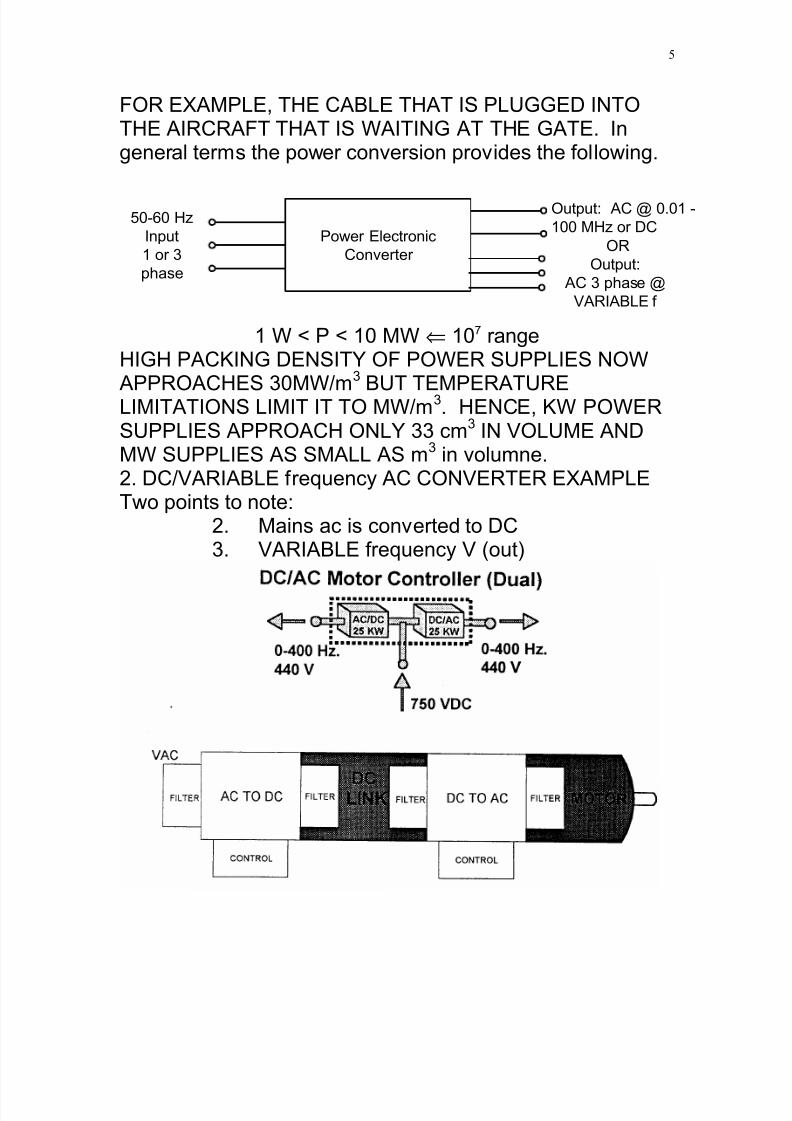
FOR EXAMPLE, THE CABLE THAT IS PLUGGED INTOTHE AIRCRAFT THAT IS WAITING AT THE GATE. Ingeneral terms the power conversion provides the following.
Power Electronic
Converter
50-60 Hz
Input
1 or 3
phase
OR
Output:
AC 3 phase @
VARIABLE f
Output: AC @ 0.01 -
100 MHz or DC
1 W < P < 10 MW ⇐ 107 rangeHIGH PACKING DENSITY OF POWER SUPPLIES NOW
APPROACHES 30MW/m
3
BUT TEMPERATURELIMITATIONS LIMIT IT TO MW/m3. HENCE, KW POWERSUPPLIES APPROACH ONLY 33 cm3 IN VOLUME ANDMW SUPPLIES AS SMALL AS m3 in volumne.2. DC/VARIABLE frequency AC CONVERTER EXAMPLETwo points to note:
2. Mains ac is converted to DC3. VARIABLE frequency V (out)
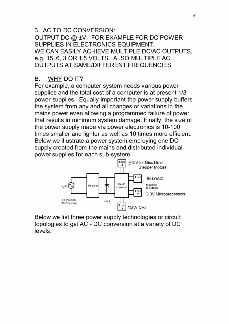
3. AC TO DC CONVERSION:OUTPUT DC @ ±V. FOR EXAMPLE FOR DC POWERSUPPLIES IN ELECTRONICS EQUIPMENT.WE CAN EASILY ACHIEVE MULTIPLE DC/AC OUTPUTS,
e.g. 15, 6, 3 OR 1.5 VOLTS. ALSO MULTIPLE ACOUTPUTS AT SAME/DIFFERENT FREQUENCIES
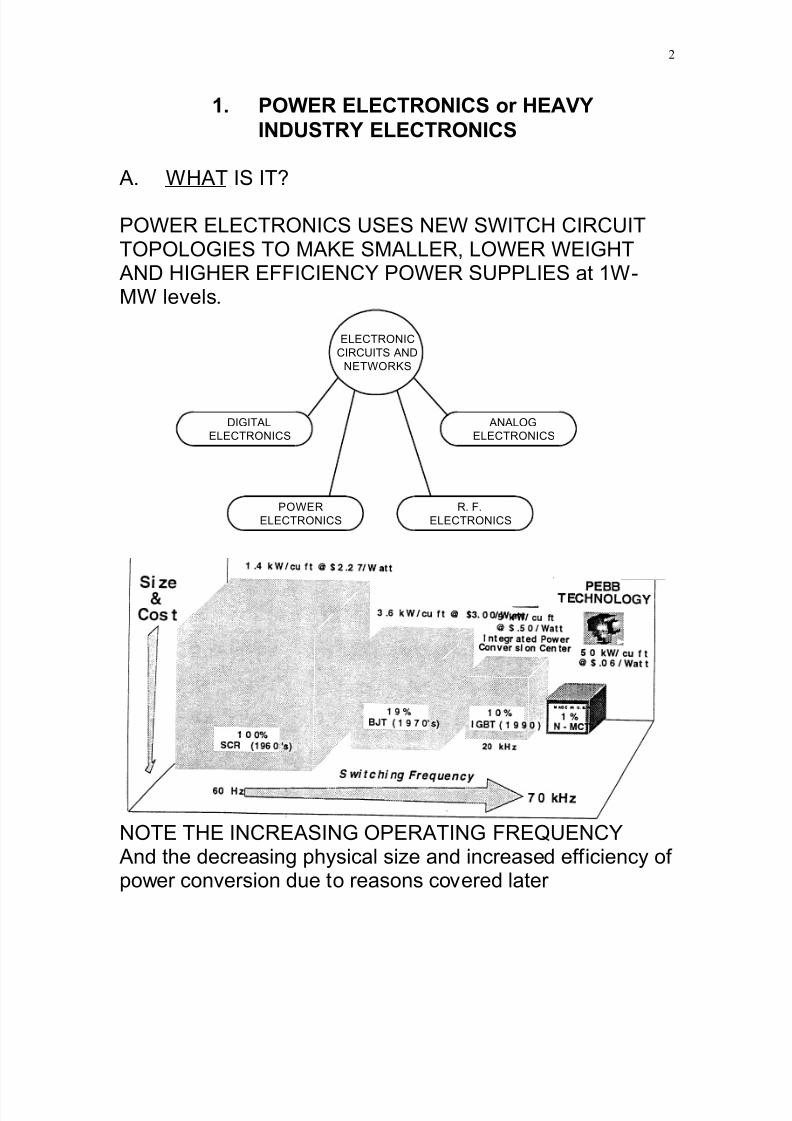
B. WHY DO IT?For example, a computer system needs various power supplies and the total cost of a computer is at present 1/3power supplies. Equally important the power supply buffersthe system from any and all changes or variations in the
mains power even allowing a programmed failure of power that results in minimum system damage. Finally, the size of the power supply made via power electronics is 10-100times smaller and lighter as well as 10 times more efficient.Below we illustrate a power system employing one DCsupply created from the mains and distributed individualpower supplies for each sub-system
Rectifier Dc-dc
converter
Load1
Load
2
vac
(t)
ac line input85-265 Vrms
dc link
regulateddc outputs
+
-
5V LOGIC
3.3V Microprocessors
Load
3 15KV CRT
Load4
+15V for Disc Drive
Stepper Motors
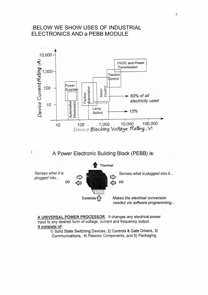
Below we list three power supply technologies or circuit
topologies to get AC - DC conversion at a variety of DClevels.
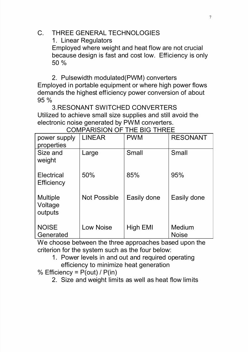
C. THREE GENERAL TECHNOLOGIES1. Linear RegulatorsEmployed where weight and heat flow are not crucialbecause design is fast and cost low. Efficiency is only
50 %
2. Pulsewidth modulated(PWM) convertersEmployed in portable equipment or where high power flowsdemands the highest efficiency power conversion of about95 %
3.RESONANT SWITCHED CONVERTERSUtilized to achieve small size supplies and still avoid the
electronic noise generated by PWM converters.COMPARISION OF THE BIG THREE
power supplyproperties
LINEAR PWM RESONANT
Size andweight
Electrical
Efficiency
MultipleVoltageoutputs
NOISEGenerated
Large
50%
Not Possible
Low Noise
Small
85%
Easily done
High EMI
Small
95%
Easily done
MediumNoise
We choose between the three approaches based upon thecriterion for the system such as the four below:
1. Power levels in and out and required operatingefficiency to minimize heat generation
% Efficiency = P(out) / P(in)2. Size and weight limits as well as heat flow limits
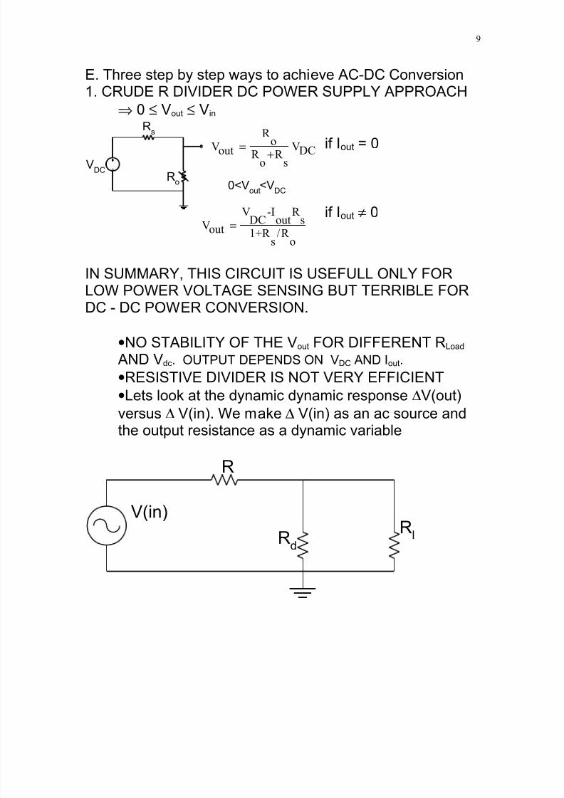
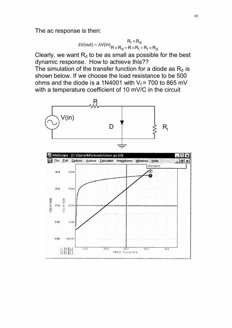
Clearly, we want Rd to be as small as possible for the bestdynamic response. How to achieve this??The simulation of the transfer function for a diode as Rd isshown below. If we choose the load resistance to be 500ohms and the diode is a 1N4001 with Vf = 700 to 865 mVwith a temperature coefficient of 10 mV/C in the circuit
WE NOW SUMMARIZE THE Limitations of the seriesregulator
•Ploss
IN CONVERSION IS Iout
*VCE
•EFFICIENCY OF CONVERSION IS Pout/Pin
•Vout > Vdc NOT POSSIBLE•OPPOSITE POLARITY OUTPUT IS NOT EASY•Zout OF V SOURCE IS DEPENDANT ON Vout
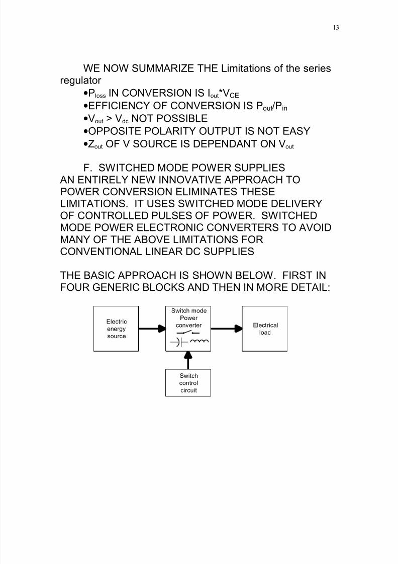
F. SWITCHED MODE POWER SUPPLIES AN ENTIRELY NEW INNOVATIVE APPROACH TOPOWER CONVERSION ELIMINATES THESELIMITATIONS. IT USES SWITCHED MODE DELIVERYOF CONTROLLED PULSES OF POWER. SWITCHEDMODE POWER ELECTRONIC CONVERTERS TO AVOIDMANY OF THE ABOVE LIMITATIONS FORCONVENTIONAL LINEAR DC SUPPLIES
THE BASIC APPROACH IS SHOWN BELOW. FIRST INFOUR GENERIC BLOCKS AND THEN IN MORE DETAIL:
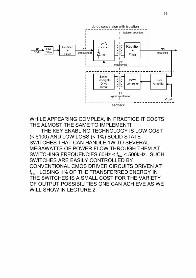
WHILE APPEARING COMPLEX, IN PRACTICE IT COSTSTHE ALMOST THE SAME TO IMPLEMENT!
THE KEY ENABLING TECHNOLOGY IS LOW COST(< $100) AND LOW LOSS (< 1%) SOLID STATESWITCHES THAT CAN HANDLE 1W TO SEVERALMEGAWATTS OF POWER FLOW THROUGH THEM ATSWITCHING FREQUENCIES 60Hz < f sw < 500kHz. SUCHSWITCHES ARE EASILY CONTROLLED BYCONVENTIONAL CMOS DRIVER CIRCUITS DRIVEN ATf sw. LOSING 1% OF THE TRANSFERRED ENERGY INTHE SWITCHES IS A SMALL COST FOR THE VARIETYOF OUTPUT POSSIBILITIES ONE CAN ACHIEVE AS WEWILL SHOW IN LECTURE 2.
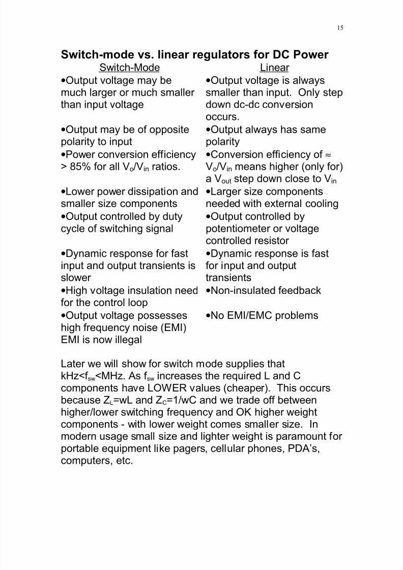
Switch-mode vs. linear regulators for DC Power Switch-Mode Linear
•Output voltage may bemuch larger or much smaller than input voltage
•Output voltage is alwayssmaller than input. Only stepdown dc-dc conversionoccurs.
•Output may be of oppositepolarity to input
•Output always has samepolarity
•Power conversion efficiency> 85% for all Vo/Vin ratios.
•Conversion efficiency of ≈
Vo/Vin means higher (only for)a Vout step down close to Vin
•Lower power dissipation andsmaller size components
•Larger size componentsneeded with external cooling
•Output controlled by dutycycle of switching signal
•Output controlled bypotentiometer or voltagecontrolled resistor
•Dynamic response for fastinput and output transients isslower •High voltage insulation need
for the control loop
•Dynamic response is fastfor input and outputtransients•Non-insulated feedback
•Output voltage possesseshigh frequency noise (EMI)EMI is now illegal
•No EMI/EMC problems
Later we will show for switch mode supplies thatkHz<f sw<MHz. As f sw increases the required L and Ccomponents have LOWER values (cheaper). This occurs
because ZL=wL and ZC=1/wC and we trade off betweenhigher/lower switching frequency and OK higher weightcomponents - with lower weight comes smaller size. Inmodern usage small size and lighter weight is paramount for portable equipment like pagers, cellular phones, PDA’s,computers, etc.
Below we compare Power In, Power Loss in Regulator andPower Output with Vinmax = 5.25 V assuming we draw 10 mAfor control:
a. Pinmax = Vinmax * Ioutmax = 5.25 V * (10 A + 10 mA) = 52.5525 Wb. The power losses in this circuit are approximately: Ploss = (Vinmax - Voutmax) * Ioutmax + 10 mA * Vin
Ploss = (5.25 V - 3.1 V) * 10 A + 5.25 V * 10 mA Ploss = [21.5 + 0.0525] W = 21.5525 W ≈ 21.5 W
c. Poutmax = Voutmax * Ioutmax = 3.1 V * 10 A = 31 W
η= Poutmax / (Pinmax) = 31 W / 52.5525 W = 0.5898 = 58.98 %
If the input voltage Vin is greater than the required outputvoltage Vout the circuit may maintain constant voltage at theoutput for different output currents. The PENTIUM PRO likemost µPs can change their supply current within one clockcycle (f clock = 266 MHz tclock = 2.76 ns) from sleep mode withvery low current (few mA) to the max power supply current(tens of A). During this transient time the power voltageshould maintain 3.1 V + 5%.No control loop can in reality maintain such performance.
The only solution is to use very strong (low ESR) bypasscapacitors at the 3.1 V output to ensure the short-termstability (ns to µs). The long-term stability (µs and longer) ismaintained by the control loop of the regulator.
Next lets see if we can do better with our power supplylosses which were 40% in this approach.
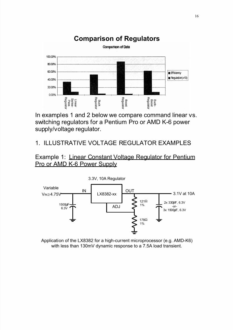
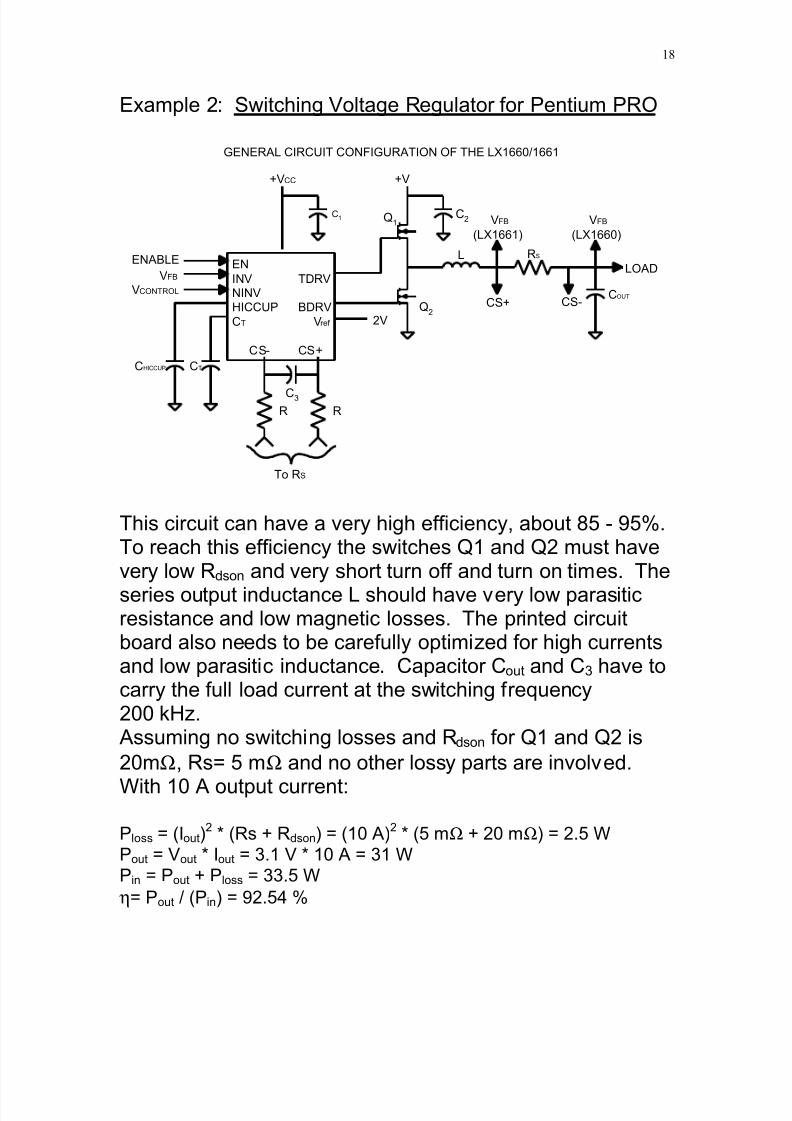
Example 2: Switching Voltage Regulator for Pentium PRO
GENERAL CIRCUIT CONFIGURATION OF THE LX1660/1661
EN
INV TDRVNINVHICCUP BDRV
CT Vref
CS- CS+
CHICCUP CT
COUT
C1
RRC3
To RS
+VCC
2V
C2
+V
L RS
CS+ CS-
VFB
(LX1661)
VFB
(LX1660)
LOAD VFB
VCONTROL
ENABLE
Q1
Q2
This circuit can have a very high efficiency, about 85 - 95%.To reach this efficiency the switches Q1 and Q2 must havevery low Rdson and very short turn off and turn on times. The
series output inductance L should have very low parasiticresistance and low magnetic losses. The printed circuitboard also needs to be carefully optimized for high currentsand low parasitic inductance. Capacitor Cout and C3 have tocarry the full load current at the switching frequency200 kHz.
Assuming no switching losses and Rdson for Q1 and Q2 is20mΩ, Rs= 5 mΩ and no other lossy parts are involved.
In reality actual efficiency values are 85% to 90% due tolosses in the parasitics.The switching regulator generates very high transients of theelectric and magnetic fields at 200 kHz. This generates both
conducted and radiated electromagnetic noise. This noisecan be easily higher than the 5% tolerance window of thesupply voltage 3.1 V for the Pentium. To avoid malfunctionof the processor it is necessary to filter this noise for allconditions. Moreover, this noise must not pollute the acmains.
Which regulator, Example 1 or 2 is a best choice for a laptop
computer?
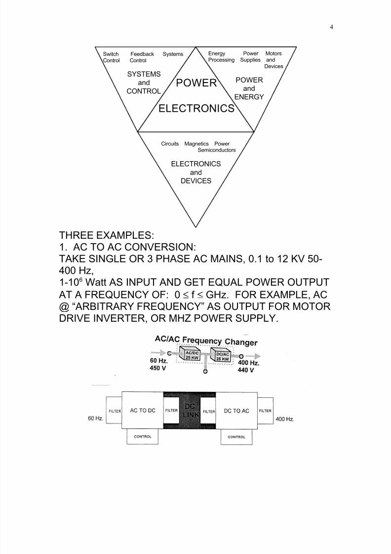
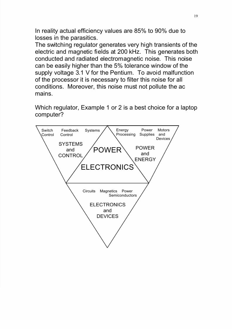
Circuits Magnetics Power Semiconductors
ELECTRONICS
andDEVICES
POWER
ELECTRONICS
Energy Power MotorsProcessing Supplies and Devices