26
Lecture 24 – Semiconductor Nanowires EECS 598-002 Winter 2006 Nanophotonics and Nano-scale Fabrication P.C.Ku
Lecture 24 –Semiconductor Nanowires
EECS 598-002 Winter 2006Nanophotonics and Nano-scale Fabrication
P.C.Ku
2EECS 598-002 Nanophotonics and Nanoscale Fabrication by P.C.Ku
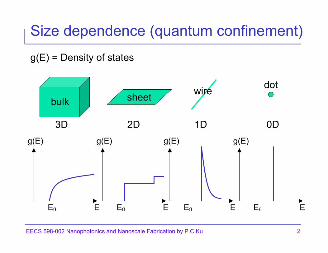
Size dependence (quantum confinement)
g(E) = Density of states
Eg E
g(E)
Eg E
g(E)
Eg E
g(E)
Eg E
g(E)
bulk sheet wire dot
3D 2D 1D 0D

3EECS 598-002 Nanophotonics and Nanoscale Fabrication by P.C.Ku
Why nanowires?
Usually easier to fabricate than QD’sMore variety of materials available.Large surface area may be useful for some applications.Can also tolerate large lattice mismatch along the interface.More easily to be made uniformNew physics: exciton diffusion, …

4EECS 598-002 Nanophotonics and Nanoscale Fabrication by P.C.Ku
Exciton diffusion
Science 273 (1996) 1351.

5EECS 598-002 Nanophotonics and Nanoscale Fabrication by P.C.Ku
VLS growth
6EECS 598-002 Nanophotonics and Nanoscale Fabrication by P.C.Ku
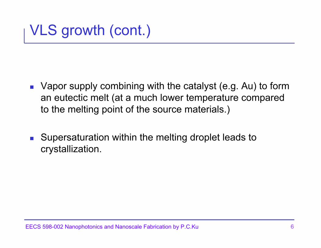
VLS growth (cont.)
Vapor supply combining with the catalyst (e.g. Au) to form an eutectic melt (at a much lower temperature compared to the melting point of the source materials.)
Supersaturation within the melting droplet leads to crystallization.
7EECS 598-002 Nanophotonics and Nanoscale Fabrication by P.C.Ku
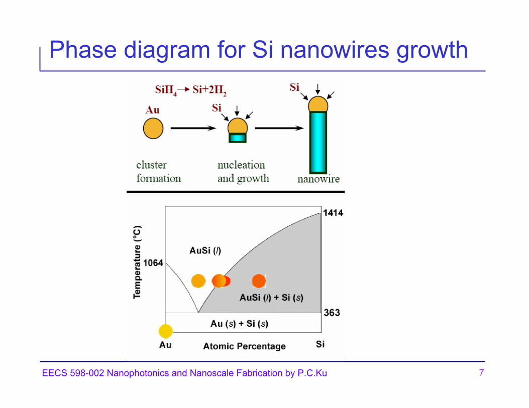
Phase diagram for Si nanowires growth

8EECS 598-002 Nanophotonics and Nanoscale Fabrication by P.C.Ku
Nanowire heterostructure
J. Appl. Phys. 97 (2005) 114325.

9EECS 598-002 Nanophotonics and Nanoscale Fabrication by P.C.Ku
Atomically abrupt interface
Gas sourceMBE
Nano Lett 2 (2002)87.
10EECS 598-002 Nanophotonics and Nanoscale Fabrication by P.C.Ku
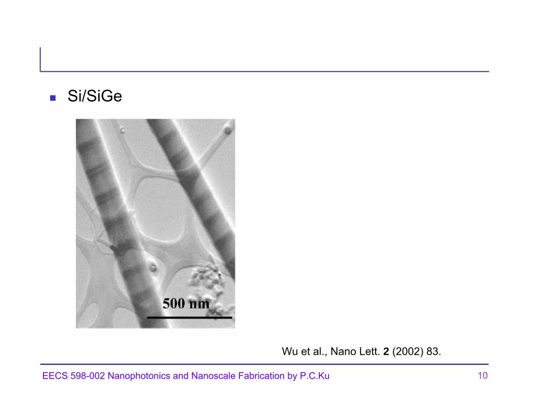
Si/SiGe
Wu et al., Nano Lett. 2 (2002) 83.

11EECS 598-002 Nanophotonics and Nanoscale Fabrication by P.C.Ku
Multishell structure
Nature 420 (2002) 57.

12EECS 598-002 Nanophotonics and Nanoscale Fabrication by P.C.Ku
13EECS 598-002 Nanophotonics and Nanoscale Fabrication by P.C.Ku
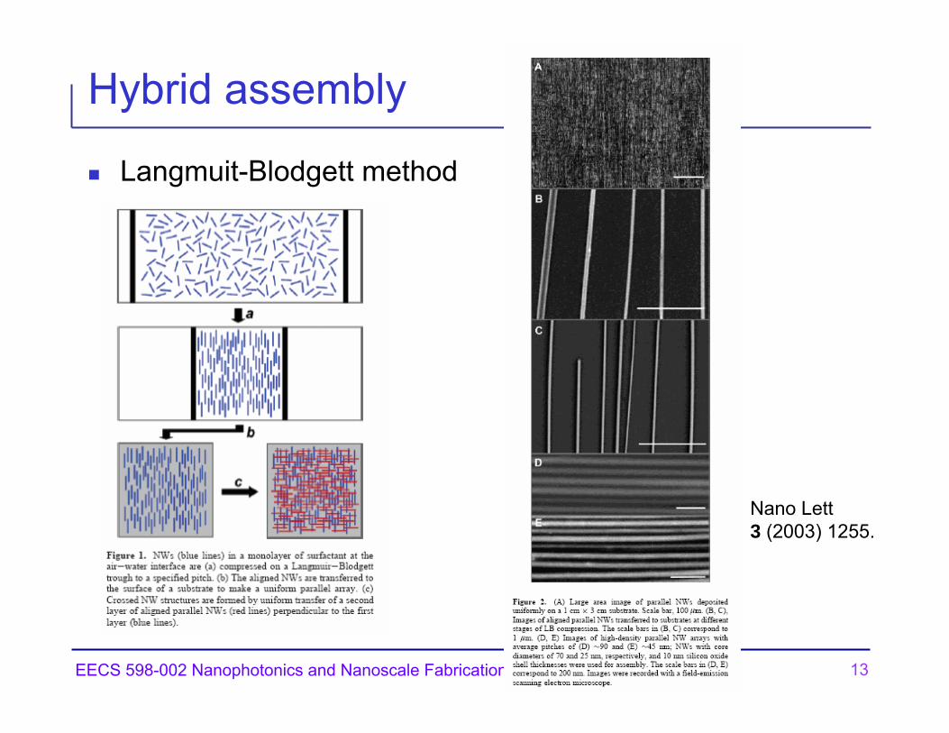
Hybrid assembly
Langmuit-Blodgett method
Nano Lett3 (2003) 1255.

14EECS 598-002 Nanophotonics and Nanoscale Fabrication by P.C.Ku
Hybrid assembly
Flow assembly
Science 291 (2001) 630.

15EECS 598-002 Nanophotonics and Nanoscale Fabrication by P.C.Ku

16EECS 598-002 Nanophotonics and Nanoscale Fabrication by P.C.Ku
17EECS 598-002 Nanophotonics and Nanoscale Fabrication by P.C.Ku
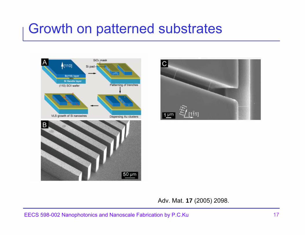
Growth on patterned substrates
Adv. Mat. 17 (2005) 2098.

18EECS 598-002 Nanophotonics and Nanoscale Fabrication by P.C.Ku
Appl. Phys. A 80 (2005) 1133.
19EECS 598-002 Nanophotonics and Nanoscale Fabrication by P.C.Ku
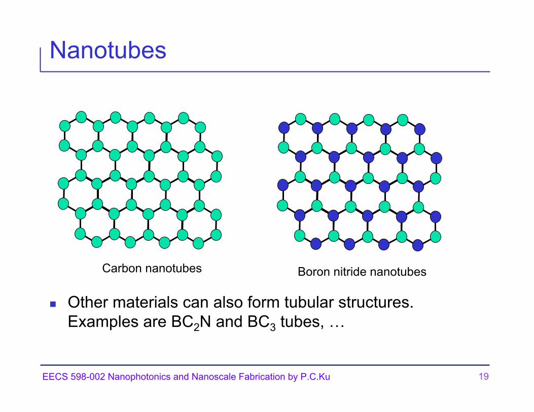
Nanotubes
Other materials can also form tubular structures. Examples are BC2N and BC3 tubes, …
Carbon nanotubes Boron nitride nanotubes

20EECS 598-002 Nanophotonics and Nanoscale Fabrication by P.C.Ku
Rolling
Zigzag face Armchair face
21EECS 598-002 Nanophotonics and Nanoscale Fabrication by P.C.Ku
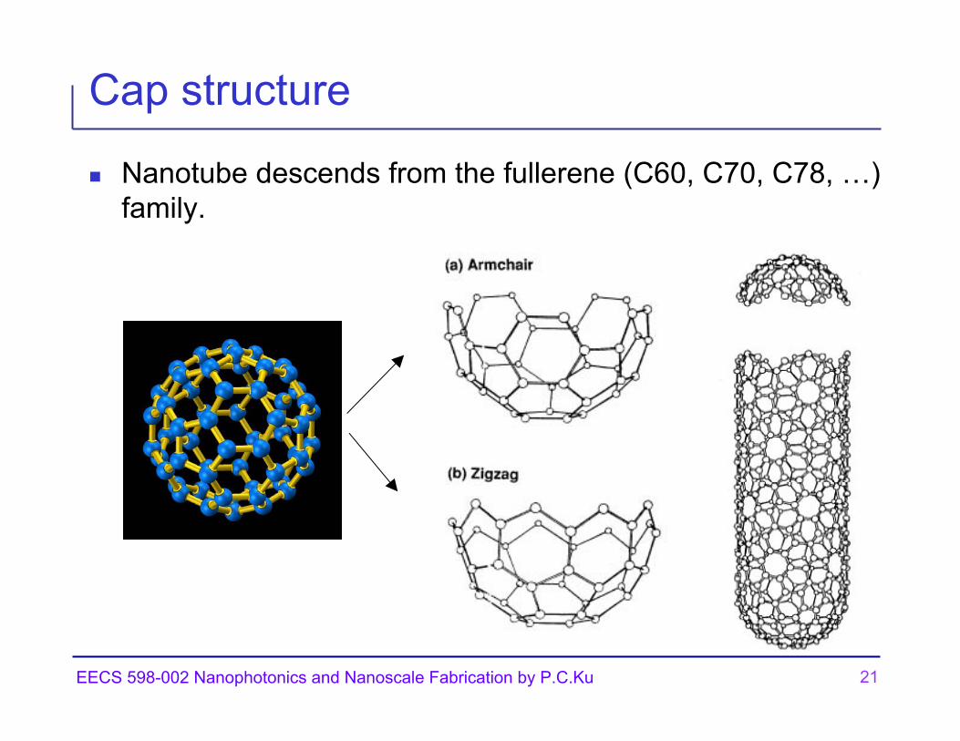
Cap structure
Nanotube descends from the fullerene (C60, C70, C78, …) family.
22EECS 598-002 Nanophotonics and Nanoscale Fabrication by P.C.Ku
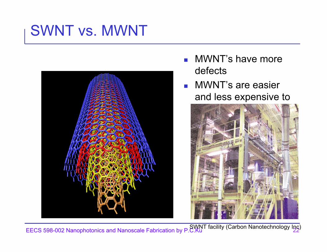
SWNT vs. MWNT
MWNT’s have more defectsMWNT’s are easier and less expensive to produce
SWNT facility (Carbon Nanotechnology Inc)
23EECS 598-002 Nanophotonics and Nanoscale Fabrication by P.C.Ku
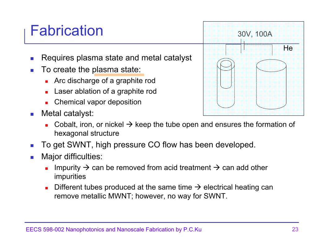
Fabrication
Requires plasma state and metal catalystTo create the plasma state:
Arc discharge of a graphite rodLaser ablation of a graphite rodChemical vapor deposition
Metal catalyst: Cobalt, iron, or nickel keep the tube open and ensures the formation of hexagonal structure
To get SWNT, high pressure CO flow has been developed.Major difficulties:
Impurity can be removed from acid treatment can add other impuritiesDifferent tubes produced at the same time electrical heating can remove metallic MWNT; however, no way for SWNT.
30V, 100A
He

24EECS 598-002 Nanophotonics and Nanoscale Fabrication by P.C.Ku
Electronic properties – Carbon tubes
SWNT: Either metal or semiconductor:Armchair : metaln-m = 3k (k ≠ 0) : semiconductor with tiny Eg
all others : semiconductor with Eg inversely proportional to tube diameter
MWNT: similar to SWNT due to weak interaction between walls

25EECS 598-002 Nanophotonics and Nanoscale Fabrication by P.C.Ku
C vs BN nanotubes
BN tubes are electrically uniformAll BN nanotubes are semiconductors and have same Egregardless of tube diameter, chirality, and number of walls.
Bulk BN is insulator cannot be used as an electrode
Bulk BN
Tungstun electrodeanode
Cu as cathode
He 650 torr

26EECS 598-002 Nanophotonics and Nanoscale Fabrication by P.C.Ku
Review article
Law et al., Ann. Rep. Mat. Res. 34 (2004) 83.


![119 Nanowires 4. Nanowires - UFAMhome.ufam.edu.br/berti/nanomateriais/Nanowires.pdf · 119 Nanowires 4. Nanowires ... written about carbon nanotubes [4.57–59], which can be ...](https://static.documents.pub/doc/80x56/5abfd11e7f8b9a5d718eba2b/119-nanowires-4-nanowires-nanowires-4-nanowires-written-about-carbon-nanotubes.jpg)


