22
Lecture #3 1 Lecture #3 VLSI Design
| Date post: | 31-Dec-2015 |
| Category: |
Documents |
| Upload: | philip-donovan |
| View: | 20 times |
| Download: | 1 times |
Lecture #3 1
Lecture #3 VLSI Design
Lecture #3 2
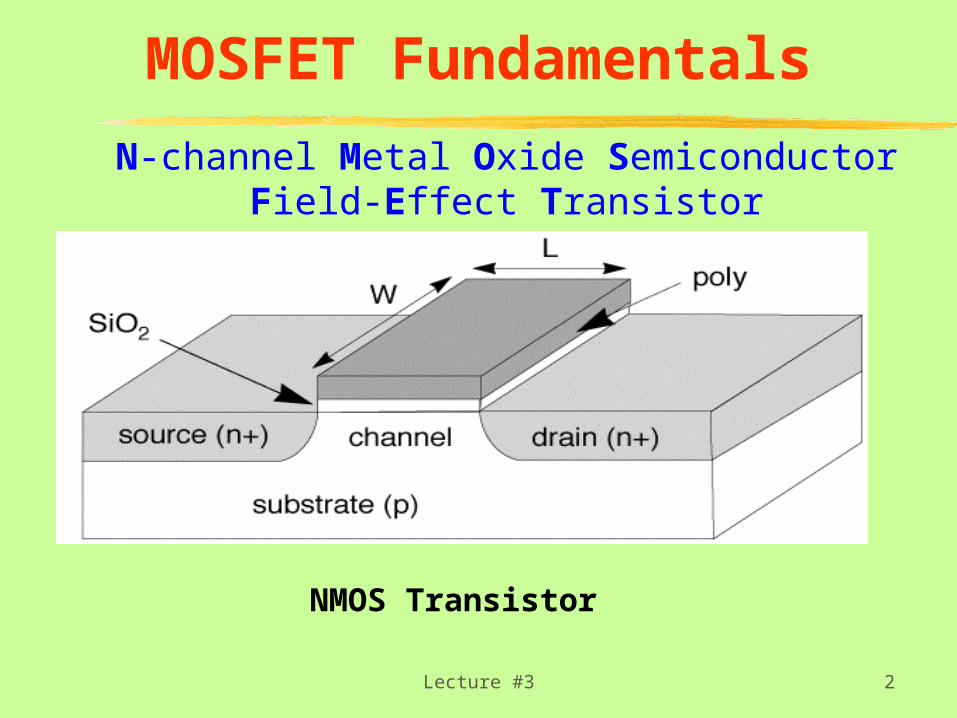
MOSFET Fundamentals
N-channel Metal Oxide Semiconductor Field-Effect Transistor
NMOS Transistor

Lecture #3 3
The MOS CapacitorLess Positive
n
More Positive Much More Positive
n << Ions
V < VT
n Ions
V VT
n >> Ions
V > VT
VT Minimum Voltage for Inversion
+
+
+++
++ ++ +++
++ + ++ +
++
++
+++
++ ++
+
++ ++++
+ +
++
++
++
++
+++
++
+
+++
+ +++
++ +
+ ++
+
Lecture #3 4
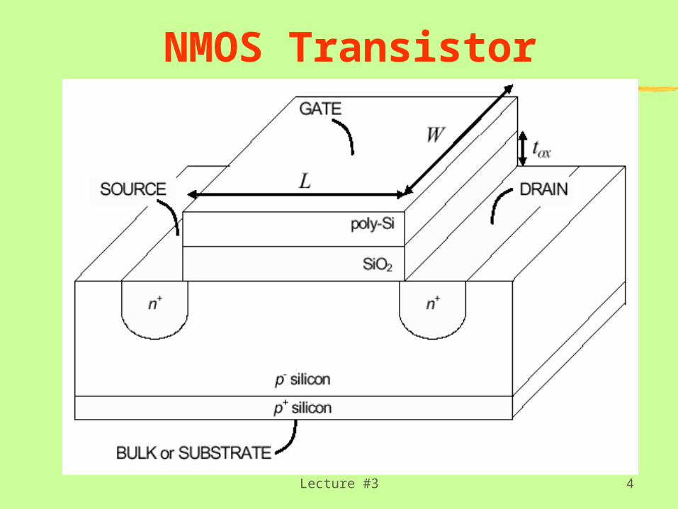
NMOS Transistor
Lecture #3 5
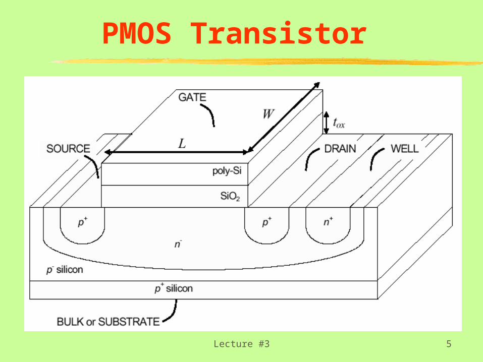
PMOS Transistor

Lecture #3 6
nMOS with VG < VT0 VD = 0

Lecture #3 7
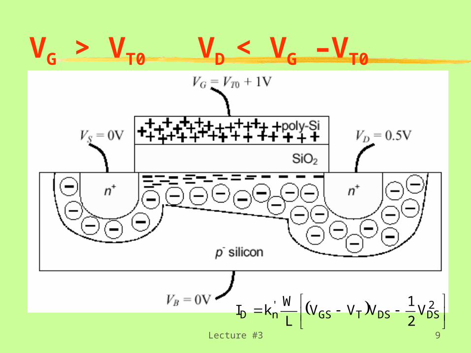
nMOS with VG > VT0 VD = 0
Lecture #3 8
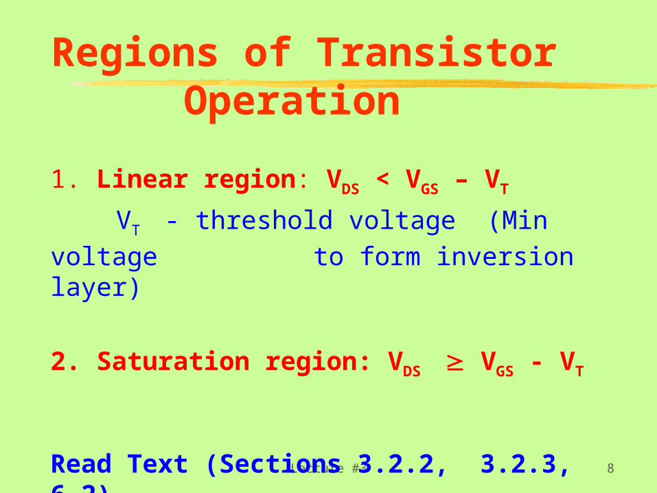
Regions of Transistor Operation
1. Linear region: VDS < VGS – VT
VT - threshold voltage (Min voltage to form inversion layer)
2. Saturation region: VDS VGS - VT
Read Text (Sections 3.2.2, 3.2.3, 6.2)
Lecture #3 9
nMOS - Linear Region with
VG > VT0 VD < VG –VT0
2
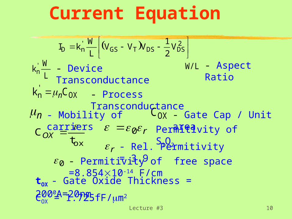
DSDSTGS'nD V
2
1VVV
L
WkI
Lecture #3 10
2
DSDSTGS'nD V
2
1VVV
L
WkI
L
Wk '
n - Device Transconductance
oxtC
OX
OX'n Ck n
n - Mobility of carriers OXC - Gate Cap / Unit area Permitivity of SiO2
tOX - Gate Oxide Thickness = 2000A=20nm
r0
0 - Permitivity of free space =8.85410-14 F/cm
r - Rel. Permitivity = 3.9
COX = 1.725fF/m2
W/L - Aspect Ratio
- Process Transconductance
Current Equation
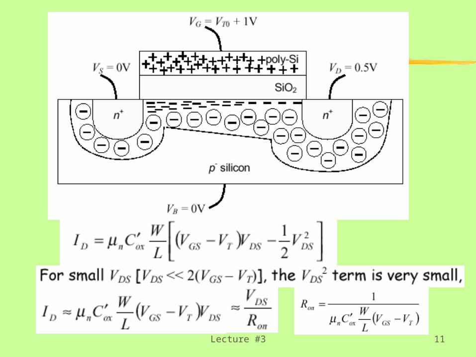
Lecture #3 11

Lecture #3 12
1.5V
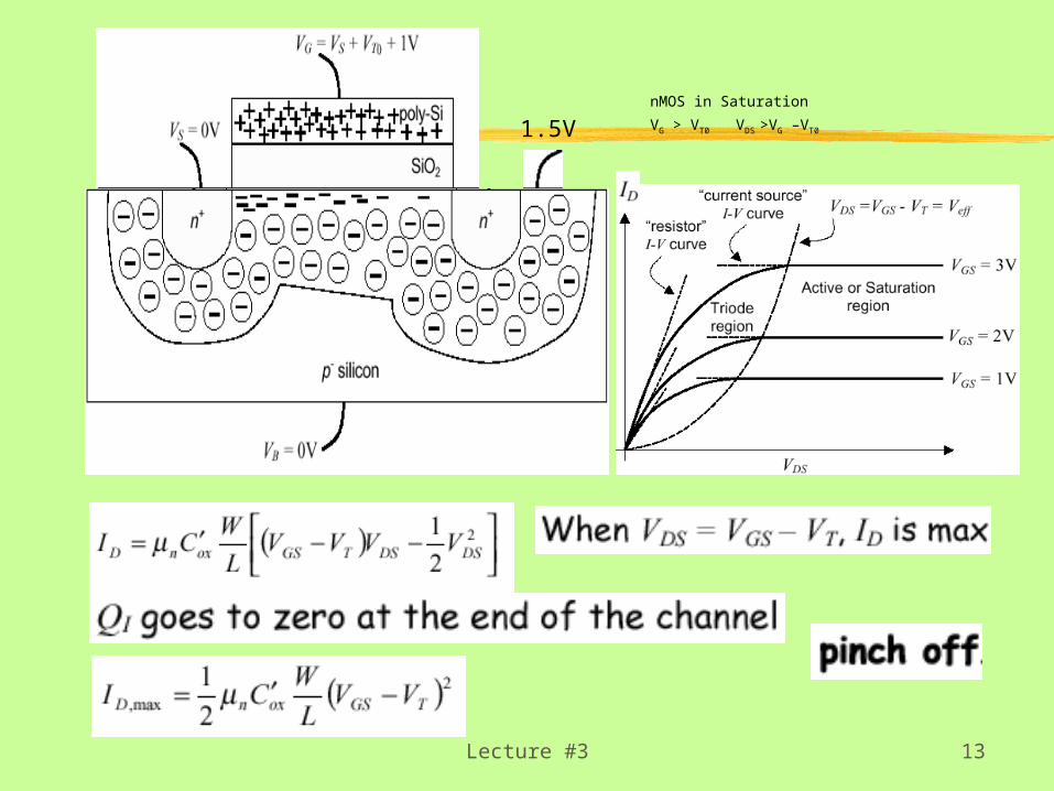
Lecture #3 13
1.5VnMOS in Saturation
VG > VT0 VDS >VG –VT0

Lecture #3 14
At ‘a’
2
DSDSTGS'nD V
2
1VVV
L
WkI
DSDSTGS'nD VV
2
1VV
L
WkI
At ‘b’
DSTGS'n
ONV
21
VVLW
k
1R
TGS'n
ONVV
LW
k
1R
1.5V
a
b
•• •c
At ‘c’ 2TGS
'n
D VVL
W
2
kI
2TGS'n
DSON
VVLW
k
V2R
Lecture #3 15
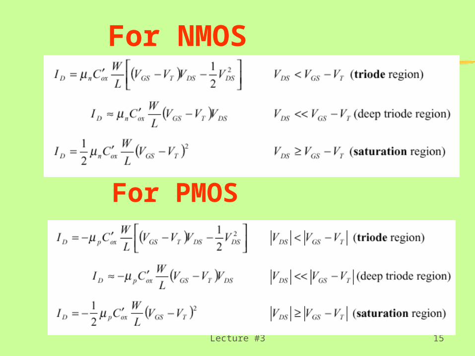
For NMOS
For PMOS
Lecture #3 16
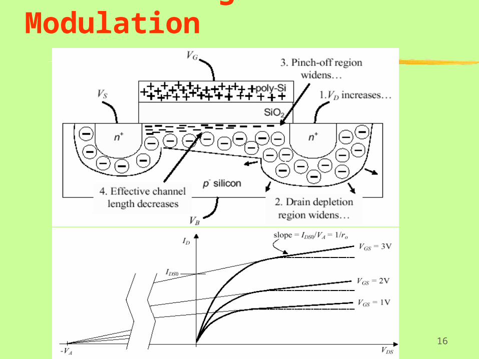
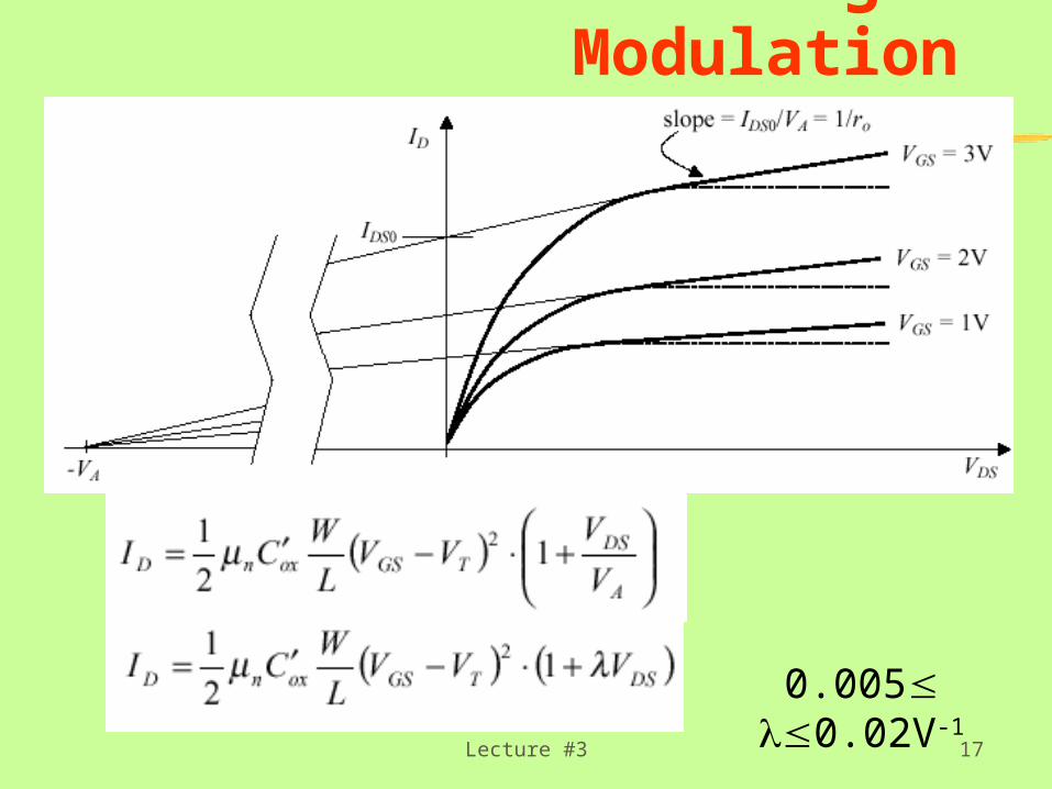
Channel Length Modulation
Lecture #3 17
Channel Length Modulation
0.005 0.02V-1

Lecture #3 18
MOSFET Symbols
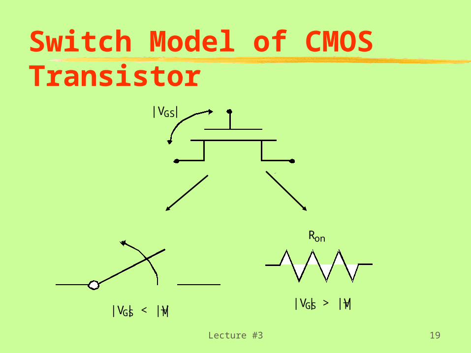
Lecture #3 19
Ron
|VGS| < |VT||VGS| > |VT|
|VGS|
Switch Model of CMOS Transistor
Lecture #3 20
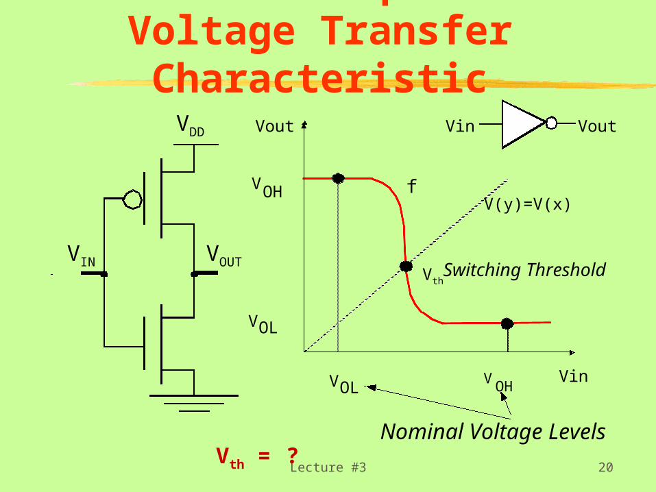
VDD
VIN VOUT
VoutVin
Vin
Vout
VOH
VOL
Vth
VOHVOL
fV(y)=V(x)
Switching Threshold
Nominal Voltage LevelsVth = ?
Inverter DC Operation Voltage Transfer
Characteristic
Lecture #3 21
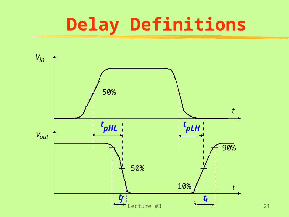
Delay Definitions
tpHL tpLH
t
t
Vin
Vout
50%
50%
tr
10%
90%
tf

Lecture #3 22
CMOS Inverter: Steady State Response
VDD
VOUT
VIN = VDD VIN = 0
RON
VOH = VDD
VOL= 0
Vth = Ronp) f(Ronn,
VDD
RON
VOUT
Threshold Voltage


