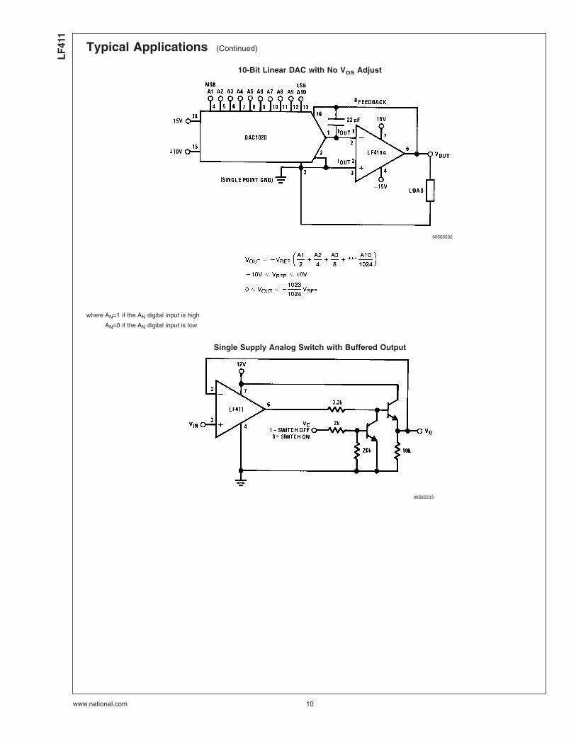
LF411Low Offset, Low Drift JFET Input Operational AmplifierGeneral DescriptionThese devices are low cost, high speed, JFET input opera-tional amplifiers with very low input offset voltage and guar-anteed input offset voltage drift. They require low supplycurrent yet maintain a large gain bandwidth product and fastslew rate. In addition, well matched high voltage JFET inputdevices provide very low input bias and offset currents. TheLF411 is pin compatible with the standard LM741 allowingdesigners to immediately upgrade the overall performance ofexisting designs.
These amplifiers may be used in applications such as highspeed integrators, fast D/A converters, sample and holdcircuits and many other circuits requiring low input offsetvoltage and drift, low input bias current, high input imped-ance, high slew rate and wide bandwidth.
Featuresn Internally trimmed offset voltage: 0.5 mV(max)n Input offset voltage drift: 10 µV/˚C(max)n Low input bias current: 50 pAn Low input noise current: 0.01 pA/√Hzn Wide gain bandwidth: 3 MHz(min)n High slew rate: 10V/µs(min)n Low supply current: 1.8 mAn High input impedance: 1012Ωn Low total harmonic distortion: ≤0.02%n Low 1/f noise corner: 50 Hzn Fast settling time to 0.01%: 2 µs
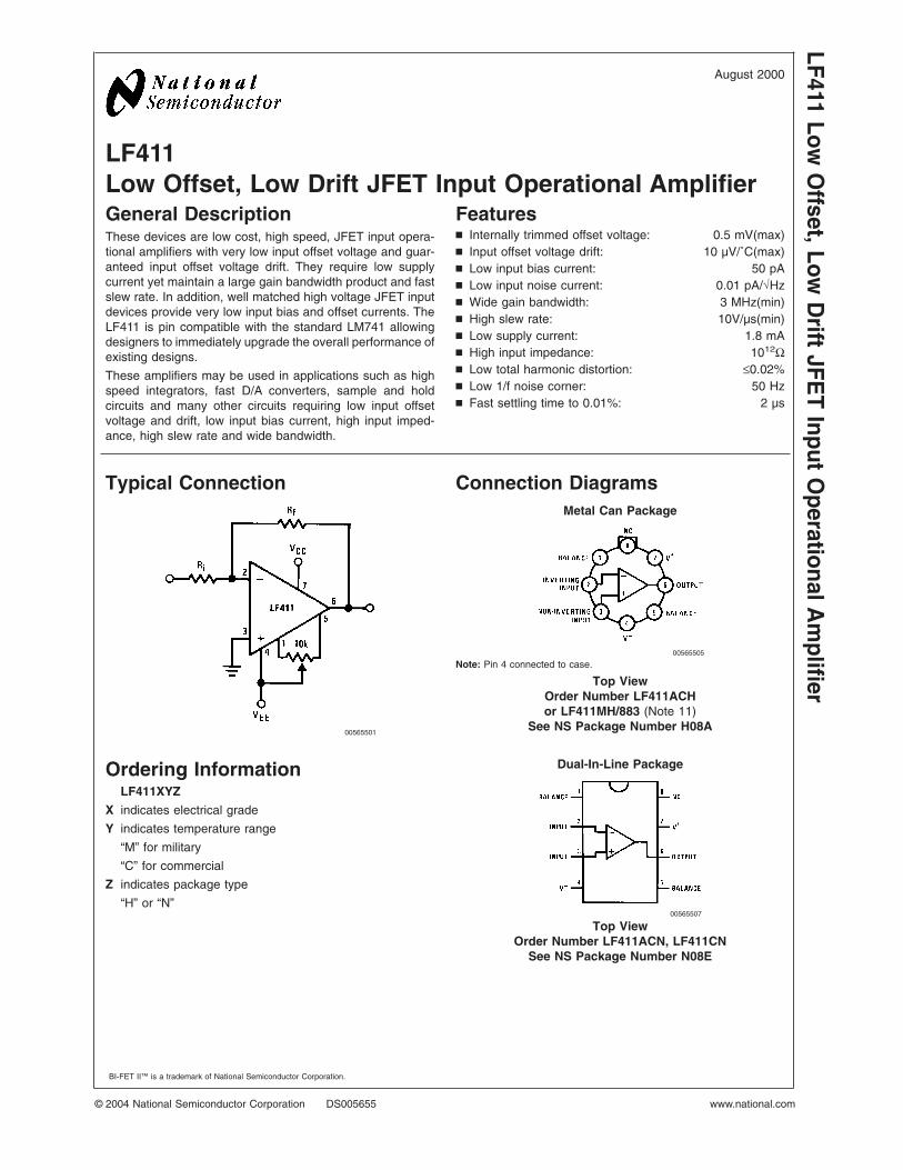
Typical Connection
00565501
Ordering InformationLF411XYZ
X indicates electrical grade
Y indicates temperature range
“M” for military
“C” for commercial
Z indicates package type
“H” or “N”
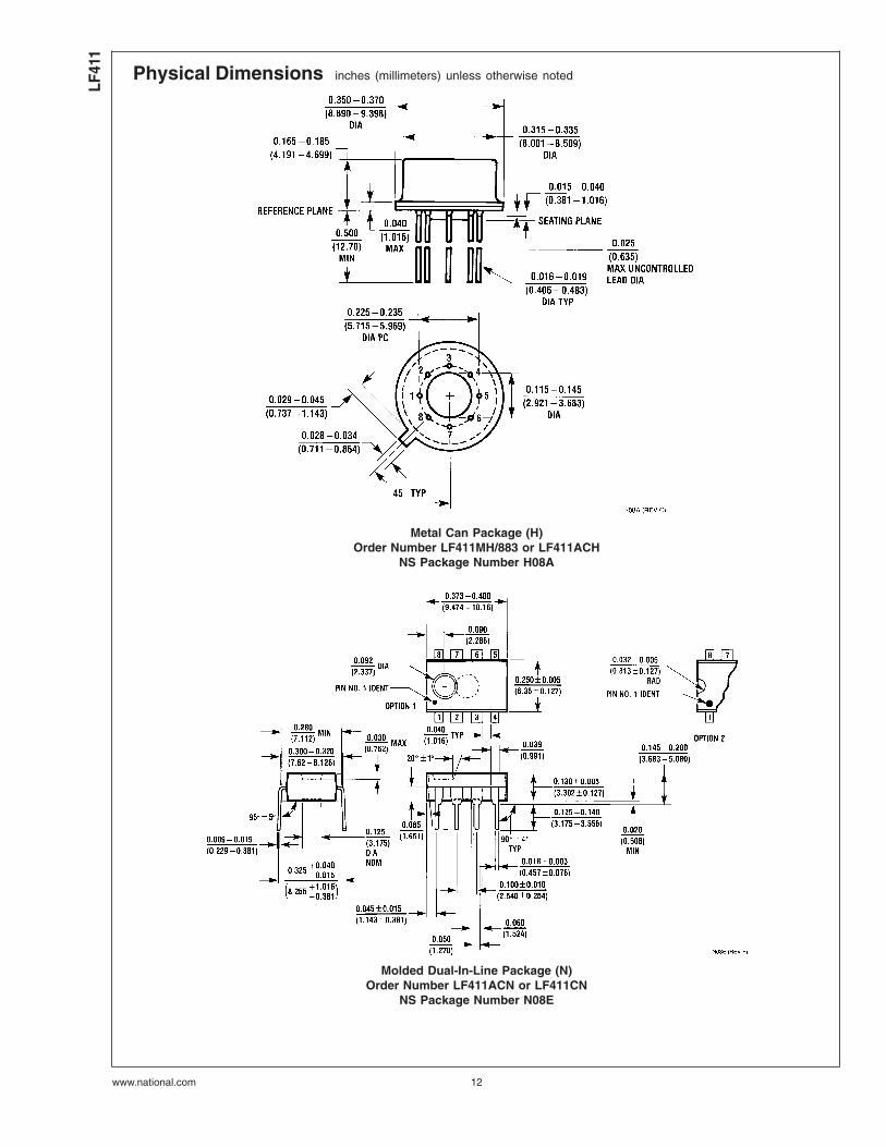
Connection DiagramsMetal Can Package
00565505
Note: Pin 4 connected to case.
Top ViewOrder Number LF411ACHor LF411MH/883 (Note 11)
See NS Package Number H08A
Dual-In-Line Package
00565507
Top ViewOrder Number LF411ACN, LF411CN
See NS Package Number N08E
BI-FET II™ is a trademark of National Semiconductor Corporation.
If Military/Aerospace specified devices are required,please contact the National Semiconductor Sales Office/Distributors for availability and specifications.
LF411A LF411
Supply Voltage ±22V ±18V
Differential Input Voltage ±38V ±30V
Input Voltage Range
(Note 2) ±19V ±15V
Output Short Circuit
Duration Continuous Continuous
H Package N Package
Power Dissipation
(Notes 3, 10) 670 mW 670 mW
H Package N Package
Tjmax 150˚C 115˚C
θjA 162˚C/W (Still Air) 120˚C/W
65˚C/W (400LF/min
Air Flow)
θjC 20˚C/W
Operating Temp.
Range (Note 4) (Note 4)
Storage Temp.
Range −65˚C≤TA≤150˚C −65˚C≤TA≤150˚C
Lead Temp.
(Soldering,10 sec.)
260˚C 260˚C
ESD Tolerance Rating to be determined.
DC Electrical Characteristics (Note 5)
Symbol Parameter Conditions LF411A LF411 Units
Min Typ Max Min Typ Max
VOS Input Offset Voltage RS=10 kΩ, TA=25˚C 0.3 0.5 0.8 2.0 mV
∆VOS/∆T Average TC of Input RS=10 kΩ (Note 6) 7 10 7 20 µV/˚C
Offset Voltage (Note 6)
IOS Input Offset Current VS=±15V Tj=25˚C 25 100 25 100 pA
(Notes 5, 7) Tj=70˚C 2 2 nA
Tj=125˚C 25 25 nA
IB Input Bias Current VS=±15V Tj=25˚C 50 200 50 200 pA
(Notes 5, 7) Tj=70˚C 4 4 nA
Tj=125˚C 50 50 nA
RIN Input Resistance Tj=25˚C 1012 1012 ΩAVOL Large Signal Voltage VS=±15V, VO=±10V, 50 200 25 200 V/mV
Gain RL=2k, TA=25˚C
Over Temperature 25 200 15 200 V/mV
VO Output Voltage Swing VS=±15V, RL=10k ±12 ±13.5 ±12 ±13.5 V
en Equivalent Input Noise Voltage TA=25˚C, RS=100Ω,f=1 kHz
25 25
in Equivalent Input Noise Current TA=25˚C, f=1 kHz 0.01 0.01
LF41
1
www.national.com 2
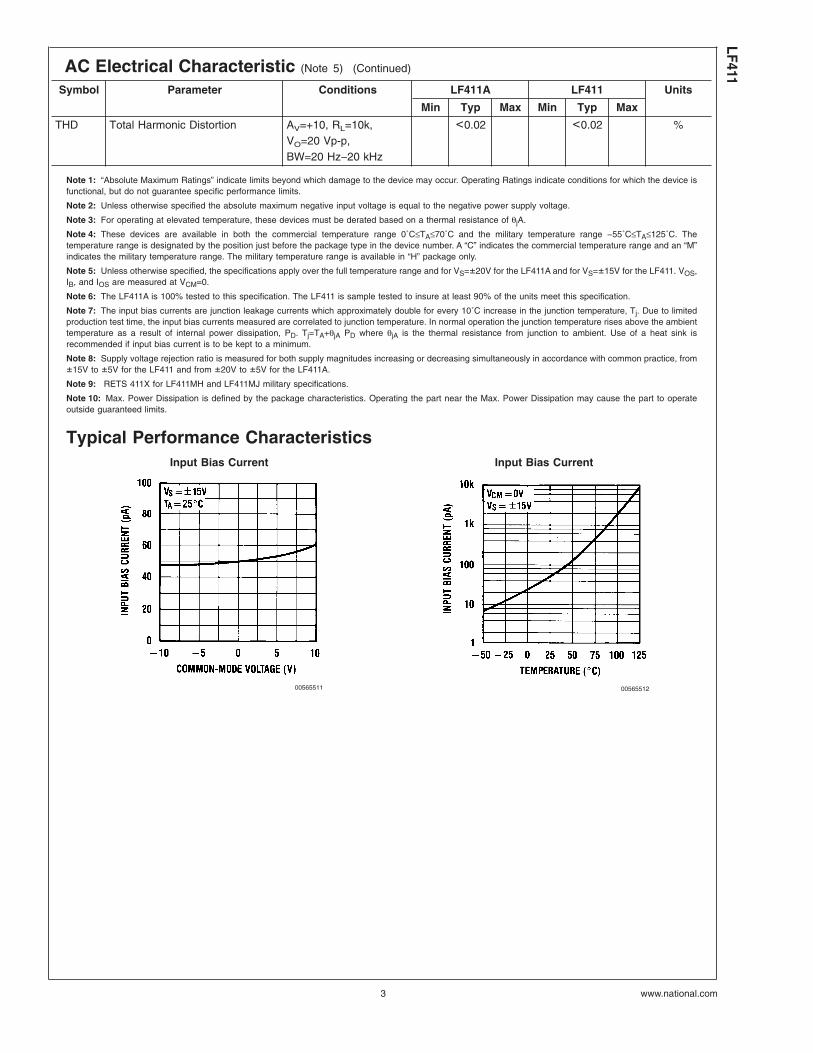
AC Electrical Characteristic (Note 5) (Continued)
Symbol Parameter Conditions LF411A LF411 Units
Min Typ Max Min Typ Max
THD Total Harmonic Distortion AV=+10, RL=10k,VO=20 Vp-p,BW=20 Hz−20 kHz
<0.02 <0.02 %
Note 1: “Absolute Maximum Ratings” indicate limits beyond which damage to the device may occur. Operating Ratings indicate conditions for which the device isfunctional, but do not guarantee specific performance limits.
Note 2: Unless otherwise specified the absolute maximum negative input voltage is equal to the negative power supply voltage.
Note 3: For operating at elevated temperature, these devices must be derated based on a thermal resistance of θjA.
Note 4: These devices are available in both the commercial temperature range 0˚C≤TA≤70˚C and the military temperature range −55˚C≤TA≤125˚C. Thetemperature range is designated by the position just before the package type in the device number. A “C” indicates the commercial temperature range and an “M”indicates the military temperature range. The military temperature range is available in “H” package only.
Note 5: Unless otherwise specified, the specifications apply over the full temperature range and for VS=±20V for the LF411A and for VS=±15V for the LF411. VOS,IB, and IOS are measured at VCM=0.
Note 6: The LF411A is 100% tested to this specification. The LF411 is sample tested to insure at least 90% of the units meet this specification.
Note 7: The input bias currents are junction leakage currents which approximately double for every 10˚C increase in the junction temperature, Tj. Due to limitedproduction test time, the input bias currents measured are correlated to junction temperature. In normal operation the junction temperature rises above the ambienttemperature as a result of internal power dissipation, PD. Tj=TA+θjA PD where θjA is the thermal resistance from junction to ambient. Use of a heat sink isrecommended if input bias current is to be kept to a minimum.
Note 8: Supply voltage rejection ratio is measured for both supply magnitudes increasing or decreasing simultaneously in accordance with common practice, from±15V to ±5V for the LF411 and from ±20V to ±5V for the LF411A.
Note 9: RETS 411X for LF411MH and LF411MJ military specifications.
Note 10: Max. Power Dissipation is defined by the package characteristics. Operating the part near the Max. Power Dissipation may cause the part to operateoutside guaranteed limits.
Typical Performance CharacteristicsInput Bias Current Input Bias Current
00565511 00565512
LF411
www.national.com3
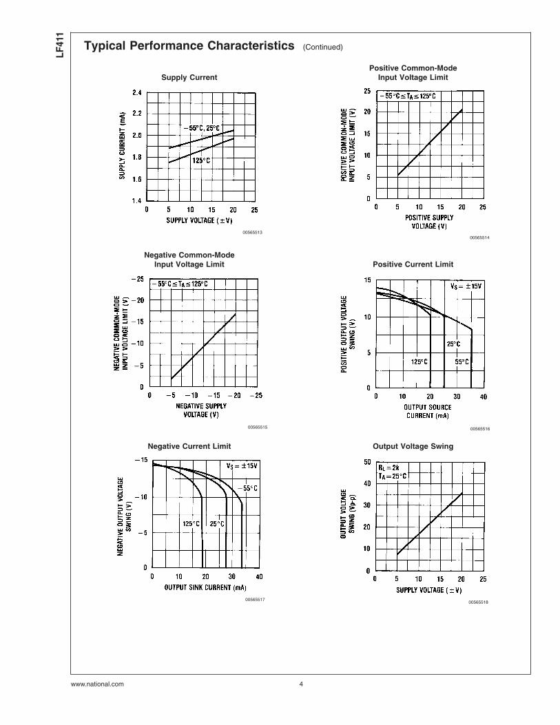
Typical Performance Characteristics (Continued)
Supply CurrentPositive Common-Mode
Input Voltage Limit
0056551300565514
Negative Common-ModeInput Voltage Limit Positive Current Limit
00565515 00565516
Negative Current Limit Output Voltage Swing
0056551700565518
LF41
1
www.national.com 4
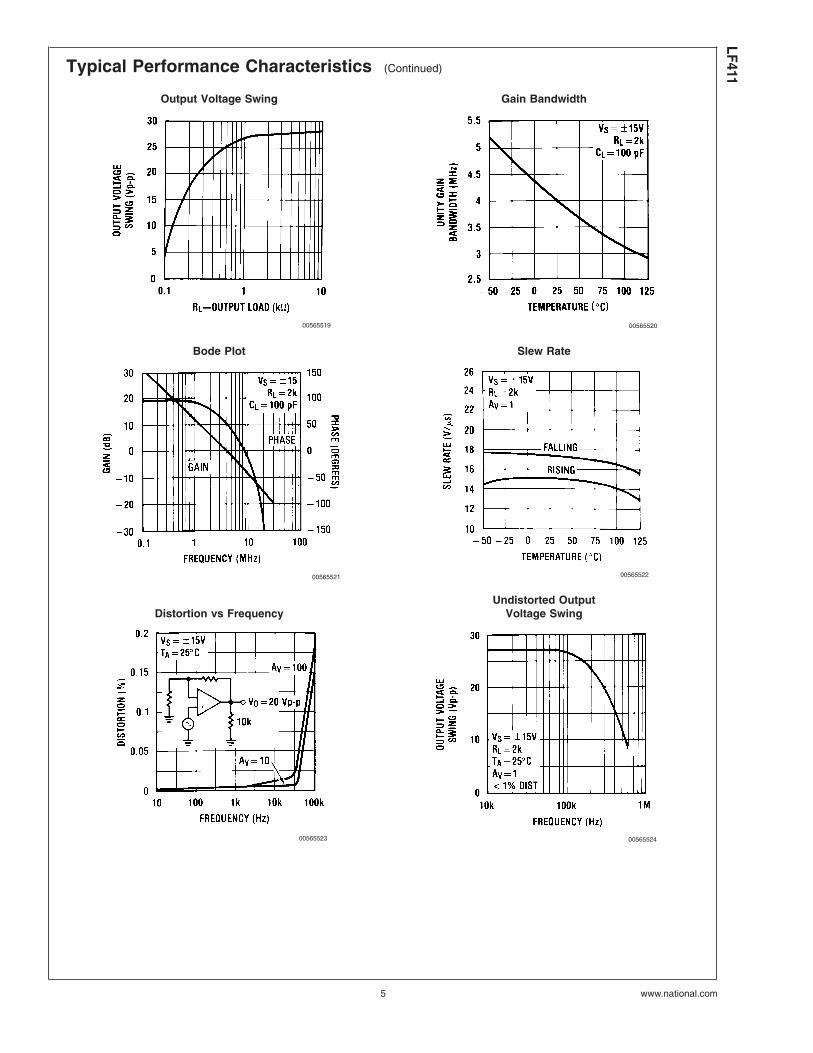
Typical Performance Characteristics (Continued)
Output Voltage Swing Gain Bandwidth
00565519 00565520
Bode Plot Slew Rate
00565521 00565522
Distortion vs FrequencyUndistorted Output
Voltage Swing
00565523 00565524
LF411
www.national.com5
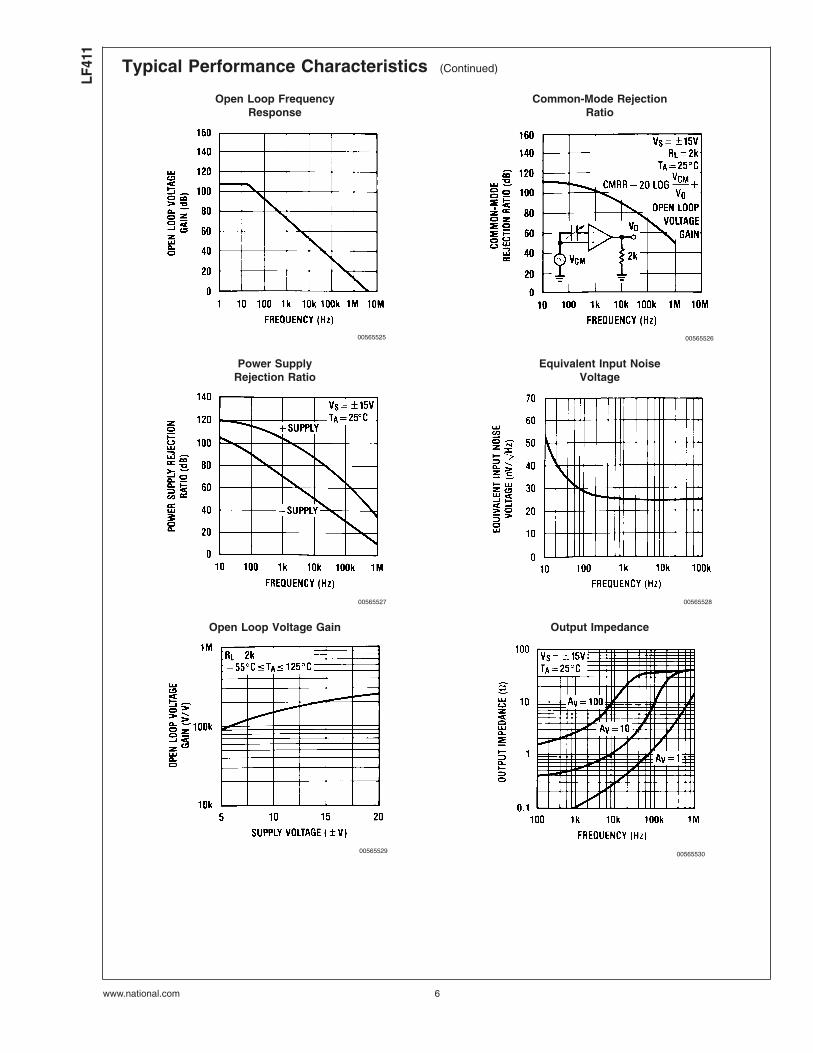
Typical Performance Characteristics (Continued)
Open Loop FrequencyResponse
Common-Mode RejectionRatio
00565525 00565526
Power SupplyRejection Ratio
Equivalent Input NoiseVoltage
00565527 00565528
Open Loop Voltage Gain Output Impedance
00565529 00565530
LF41
1
www.national.com 6
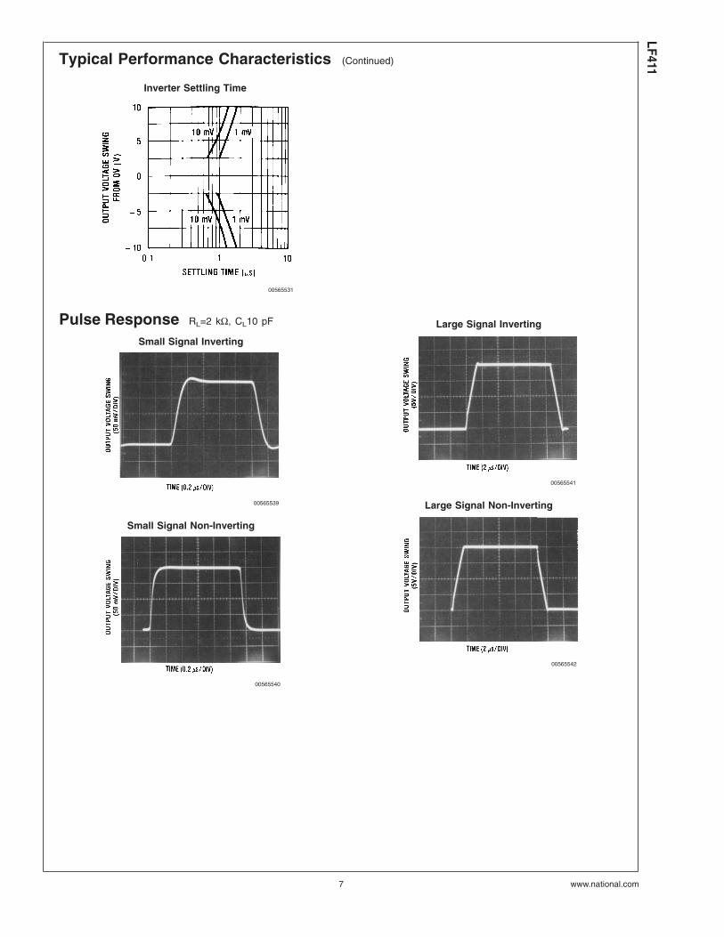
Typical Performance Characteristics (Continued)
Inverter Settling Time
00565531
Pulse Response RL=2 kΩ, CL10 pF
Small Signal Inverting
00565539
Small Signal Non-Inverting
00565540
Large Signal Inverting
00565541
Large Signal Non-Inverting
00565542
LF411
www.national.com7
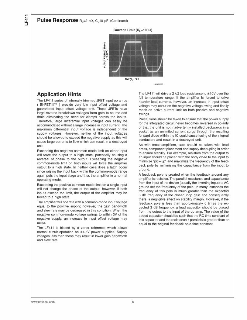
Pulse Response RL=2 kΩ, CL10 pF (Continued)
Current Limit (RL=100Ω)
00565543
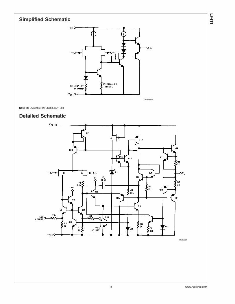
Application HintsThe LF411 series of internally trimmed JFET input op amps( BI-FET II™ ) provide very low input offset voltage andguaranteed input offset voltage drift. These JFETs havelarge reverse breakdown voltages from gate to source anddrain eliminating the need for clamps across the inputs.Therefore, large differential input voltages can easily beaccommodated without a large increase in input current. Themaximum differential input voltage is independent of thesupply voltages. However, neither of the input voltagesshould be allowed to exceed the negative supply as this willcause large currents to flow which can result in a destroyedunit.
Exceeding the negative common-mode limit on either inputwill force the output to a high state, potentially causing areversal of phase to the output. Exceeding the negativecommon-mode limit on both inputs will force the amplifieroutput to a high state. In neither case does a latch occursince raising the input back within the common-mode rangeagain puts the input stage and thus the amplifier in a normaloperating mode.
Exceeding the positive common-mode limit on a single inputwill not change the phase of the output; however, if bothinputs exceed the limit, the output of the amplifier may beforced to a high state.
The amplifier will operate with a common-mode input voltageequal to the positive supply; however, the gain bandwidthand slew rate may be decreased in this condition. When thenegative common-mode voltage swings to within 3V of thenegative supply, an increase in input offset voltage mayoccur.
The LF411 is biased by a zener reference which allowsnormal circuit operation on ±4.5V power supplies. Supplyvoltages less than these may result in lower gain bandwidthand slew rate.
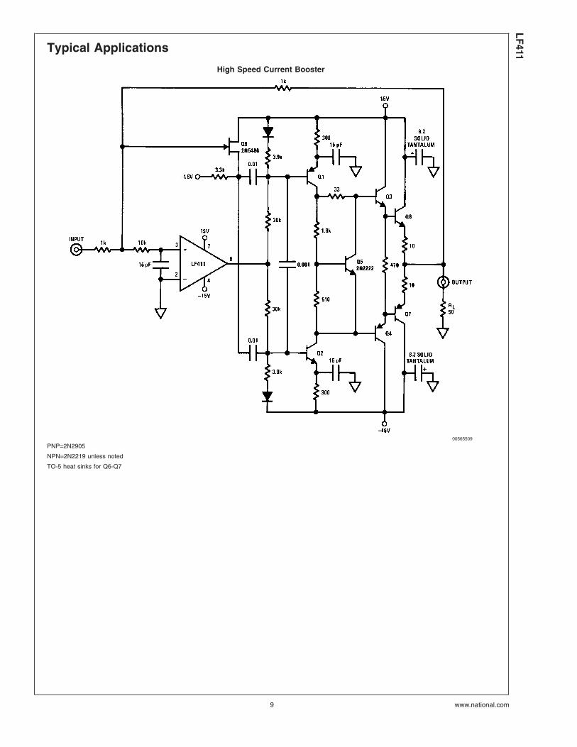
The LF411 will drive a 2 kΩ load resistance to ±10V over thefull temperature range. If the amplifier is forced to driveheavier load currents, however, an increase in input offsetvoltage may occur on the negative voltage swing and finallyreach an active current limit on both positive and negativeswings.
Precautions should be taken to ensure that the power supplyfor the integrated circuit never becomes reversed in polarityor that the unit is not inadvertently installed backwards in asocket as an unlimited current surge through the resultingforward diode within the IC could cause fusing of the internalconductors and result in a destroyed unit.
As with most amplifiers, care should be taken with leaddress, component placement and supply decoupling in orderto ensure stability. For example, resistors from the output toan input should be placed with the body close to the input tominimize “pick-up” and maximize the frequency of the feed-back pole by minimizing the capacitance from the input toground.
A feedback pole is created when the feedback around anyamplifier is resistive. The parallel resistance and capacitancefrom the input of the device (usually the inverting input) to ACground set the frequency of the pole. In many instances thefrequency of this pole is much greater than the expected3 dB frequency of the closed loop gain and consequentlythere is negligible effect on stability margin. However, if thefeedback pole is less than approximately 6 times the ex-pected 3 dB frequency, a lead capacitor should be placedfrom the output to the input of the op amp. The value of theadded capacitor should be such that the RC time constant ofthis capacitor and the resistance it parallels is greater than orequal to the original feedback pole time constant.
Metal Can Package (H)Order Number LF411MH/883 or LF411ACH
NS Package Number H08A
Molded Dual-In-Line Package (N)Order Number LF411ACN or LF411CN
NS Package Number N08E
LF41
1
www.national.com 12
Notes
LIFE SUPPORT POLICY
NATIONAL’S PRODUCTS ARE NOT AUTHORIZED FOR USE AS CRITICAL COMPONENTS IN LIFE SUPPORTDEVICES OR SYSTEMS WITHOUT THE EXPRESS WRITTEN APPROVAL OF THE PRESIDENT AND GENERALCOUNSEL OF NATIONAL SEMICONDUCTOR CORPORATION. As used herein:
1. Life support devices or systems are devices orsystems which, (a) are intended for surgical implantinto the body, or (b) support or sustain life, andwhose failure to perform when properly used inaccordance with instructions for use provided in thelabeling, can be reasonably expected to result in asignificant injury to the user.
2. A critical component is any component of a lifesupport device or system whose failure to performcan be reasonably expected to cause the failure ofthe life support device or system, or to affect itssafety or effectiveness.
BANNED SUBSTANCE COMPLIANCE
National Semiconductor certifies that the products and packing materials meet the provisions of the Customer ProductsStewardship Specification (CSP-9-111C2) and the Banned Substances and Materials of Interest Specification(CSP-9-111S2) and contain no ‘‘Banned Substances’’ as defined in CSP-9-111S2.
National SemiconductorAmericas CustomerSupport CenterEmail: [email protected]: 1-800-272-9959
National SemiconductorEurope Customer Support Center
National SemiconductorAsia Pacific CustomerSupport CenterEmail: [email protected]
National SemiconductorJapan Customer Support CenterFax: 81-3-5639-7507Email: [email protected]: 81-3-5639-7560
www.national.com
LF411Low
Offset,Low
Drift
JFET
InputO
perationalAm
plifier
National does not assume any responsibility for use of any circuitry described, no circuit patent licenses are implied and National reserves the right at any time without notice to change said circuitry and specifications.