83
1 Combinational Logic Logic and Digital System Design - CS 303 Erkay Savaş Sabanci University
| Date post: | 30-Aug-2018 |
| Category: |
Documents |
| Upload: | nguyencong |
| View: | 223 times |
| Download: | 0 times |

1
Combinational Logic
Logic and Digital System Design - CS 303Erkay Savaş
Sabanci University
2
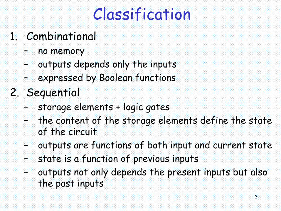
Classification1. Combinational
– no memory– outputs depends only the inputs– expressed by Boolean functions
2. Sequential– storage elements + logic gates– the content of the storage elements define the state
of the circuit– outputs are functions of both input and current state – state is a function of previous inputs– outputs not only depends the present inputs but also
the past inputs

3
Combinational Circuits
– n input bits 2n possible binary input combinations– For each possible input combination, there is one
possible output value • truth table• Boolean function (with n input variable)
– Examples: adders, subtractors, comparators, decoders, encoders, and multiplexers. • MSI• Standards cells in VLSI
Combinationalcircuit
(logic gates)
n binaryinputs
m binaryoutputs
4
Analysis & Design of Combinational Logic
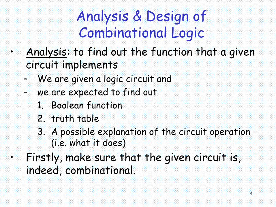
• Analysis: to find out the function that a given circuit implements– We are given a logic circuit and– we are expected to find out
1. Boolean function2. truth table3. A possible explanation of the circuit operation
(i.e. what it does)• Firstly, make sure that the given circuit is,
indeed, combinational.

5
Analysis of Combinational Logic– Verifying the circuit is combinational
• No memory elements• No feedback paths (connections)
• Secondly, obtain the Boolean functions for each output or the truth table
• Lastly, interpret the operation of the circuit from the derived Boolean functions or truth table– What is it the circuit doing? – Addition, subtraction, multiplication, etc.
6
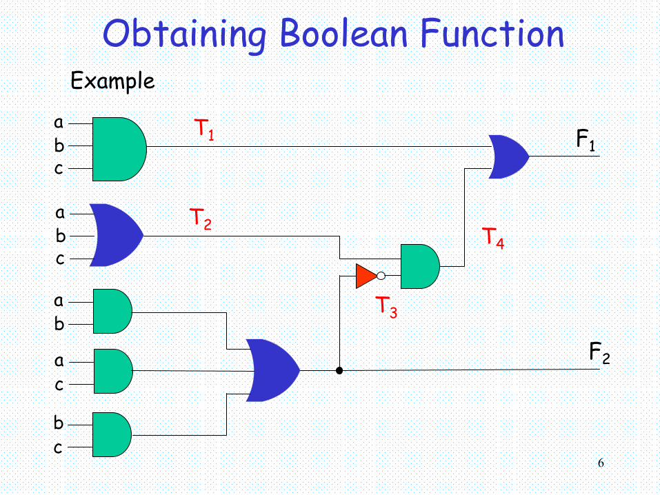
Obtaining Boolean Function
abc
abc
ab
ac
bc
F1
F2
T1
T2
T3
T4
Example

7
Example: Obtaining Boolean Function• Boolean expressions for named wires
– T1 = abc– T2 = a + b + c– F2 = ab + ac + bc– T3 = F2’ = (ab + ac + bc)’– T4 = T3T2 = (ab + ac + bc)’ (a + b + c)– F1 = T1 + T4
= abc + (ab + ac + bc)’ (a + b + c)= abc + ((a’ + b’)(a’ + c’)(b’ + c’)) (a + b + c)= abc + ((a’ + a’c’ + a’b’ + b’c’)(b’ + c’)) (a + b + c)= abc + (a’b’ + a’c’ + a’b’c’ + a’b’ + a’b’c’ + b’c’ +
b’c’) (a + b + c)

8
Example: Obtaining Boolean Function
• Boolean expressions for outputs– F2 = ab + ac + bc– F1 = abc + (a’b’ + a’c’ + a’b’c’ + b’c’) (a + b + c)– F1 = abc + a’b’c + a’bc’ + ab’c’– F1 = a(bc + b’c’) + a’(b’c + bc’)– F1 = a(b ⊕ c)’ + a’(b ⊕ c)– F1 = a ⊕ b ⊕ c

9
Example: Obtaining Truth Table
110011111010010011010010101101110001010010110101110010101110100000100000F1F2T4T3T2T1cba
sumcarry
This is what we called full-adder (FA)

10
Design of Combinational Logic• Design Procedure:
– We start with the verbal specification about what the resulting circuit will do for us (i.e. which function it will implement)
– We are expected to find 1. firstly, a Boolean function (or truth table) to
realize the desired functionality2. Logic circuit implementing the Boolean function
(or the truth table)

11
Possible Design Steps1. Find out the number of inputs and outputs2. Derive the truth table that defines the
required relationship between inputs and outputs
3. Obtain the simplified Boolean functions for each output
4. Draw the logic diagram5. Verify the correctness of the design• Specifications are often verbal, and very likely
incomplete and faulty• Wrong interpretations can result in incorrect
circuit
12
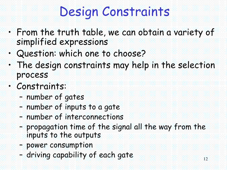
Design Constraints• From the truth table, we can obtain a variety of
simplified expressions• Question: which one to choose?• The design constraints may help in the selection
process• Constraints:
– number of gates– number of inputs to a gate– number of interconnections– propagation time of the signal all the way from the
inputs to the outputs– power consumption– driving capability of each gate
13
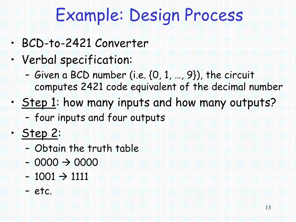
Example: Design Process• BCD-to-2421 Converter• Verbal specification:
– Given a BCD number (i.e. {0, 1, …, 9}), the circuit computes 2421 code equivalent of the decimal number
• Step 1: how many inputs and how many outputs?– four inputs and four outputs
• Step 2:– Obtain the truth table– 0000 0000– 1001 1111– etc.

14
BCD-to-2421 Converter• Truth Table
0111000111111001
1011111000110110110110100010001011001100010001001000100000000000tzyxDCBA
OutputsInputs

15
BCD-to-2421 Converter
XXXXXX
11
11100000
10
11
01
00
10110100CD
AB
• Step 3: Obtain simplified Boolean expressions for each output
• Ouput x:
x = BC + BD + AB’

16
Boolean Expressions for Outputs
XX1110XXXX1111010100000010110100
CDAB
XX1110XXXX1100100111000010110100
CDAB
y = A + BD’ + BC
z = A + B’C + BC’D

17
Boolean Expressions for Outputs
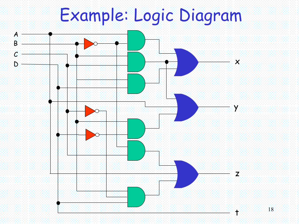
• Step 4: Draw the logic diagram
XX1010XXXX1101100101100010110100
CDAB
t = D
x = BC + BD + AB’y = A + BD’ + BCz = A + B’C + BC’D
18
Example: Logic DiagramABCD x
y
z
t
19
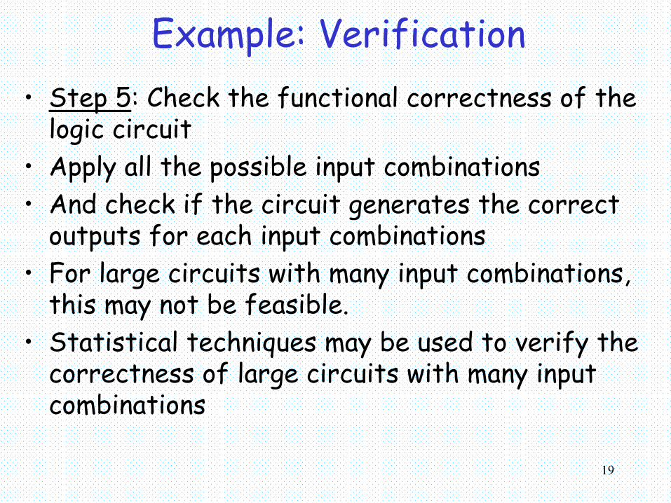
Example: Verification• Step 5: Check the functional correctness of the
logic circuit• Apply all the possible input combinations • And check if the circuit generates the correct
outputs for each input combinations• For large circuits with many input combinations,
this may not be feasible.• Statistical techniques may be used to verify the
correctness of large circuits with many input combinations
20
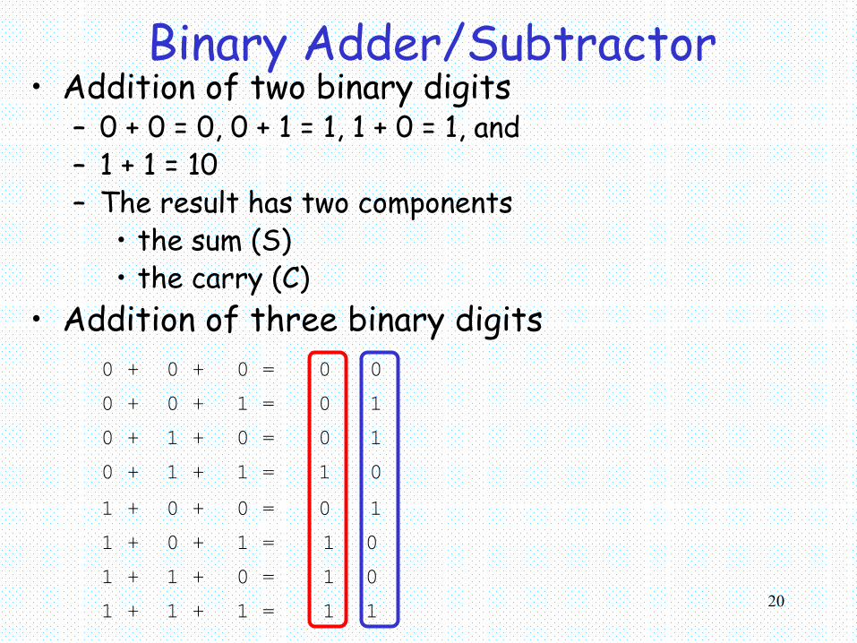
Binary Adder/Subtractor• Addition of two binary digits
– 0 + 0 = 0, 0 + 1 = 1, 1 + 0 = 1, and– 1 + 1 = 10– The result has two components
• the sum (S)• the carry (C)
• Addition of three binary digits
1 11 =1 +1 +1 00 =1 +1 +1 01 =0 +1 +0 10 =0 +1 +1 01 =1 +0 +0 10 =1 +0 +0 11 =0 +0 +0 00 =0 +0 +
21
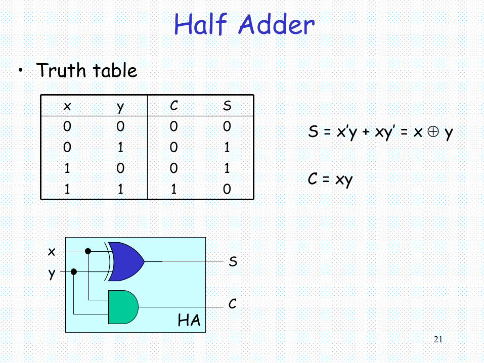
Half Adder• Truth table
0111100110100000SCyx
S = x’y + xy’ = x ⊕ y
C = xy
xy
S
CHA

22
Full Adder• A circuit that performs the arithmetic sum of
three bits– Three inputs– the range of output is [0, 3]– Two binary outputs
1111101011011011000101110100101010000000SCzyx
23
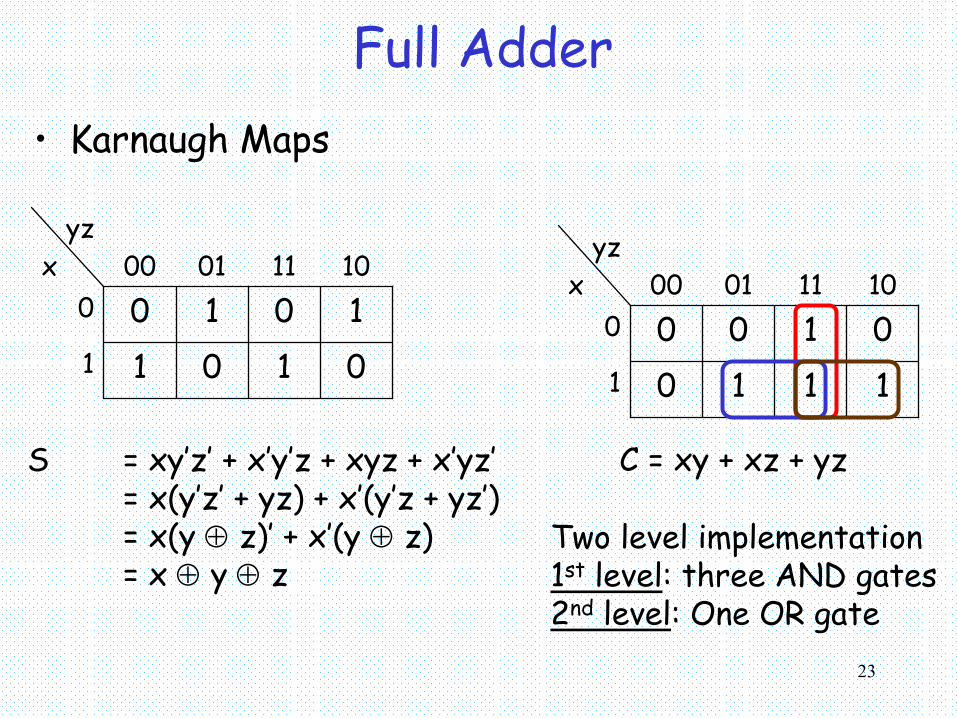
Full Adder• Karnaugh Maps
01011
1010010110100
yzx
S = xy’z’ + x’y’z + xyz + x’yz’= x(y’z’ + yz) + x’(y’z + yz’)= x(y ⊕ z)’ + x’(y ⊕ z)= x ⊕ y ⊕ z
11101
0100010110100
yzx
C = xy + xz + yz
Two level implementation1st level: three AND gates2nd level: One OR gate
24
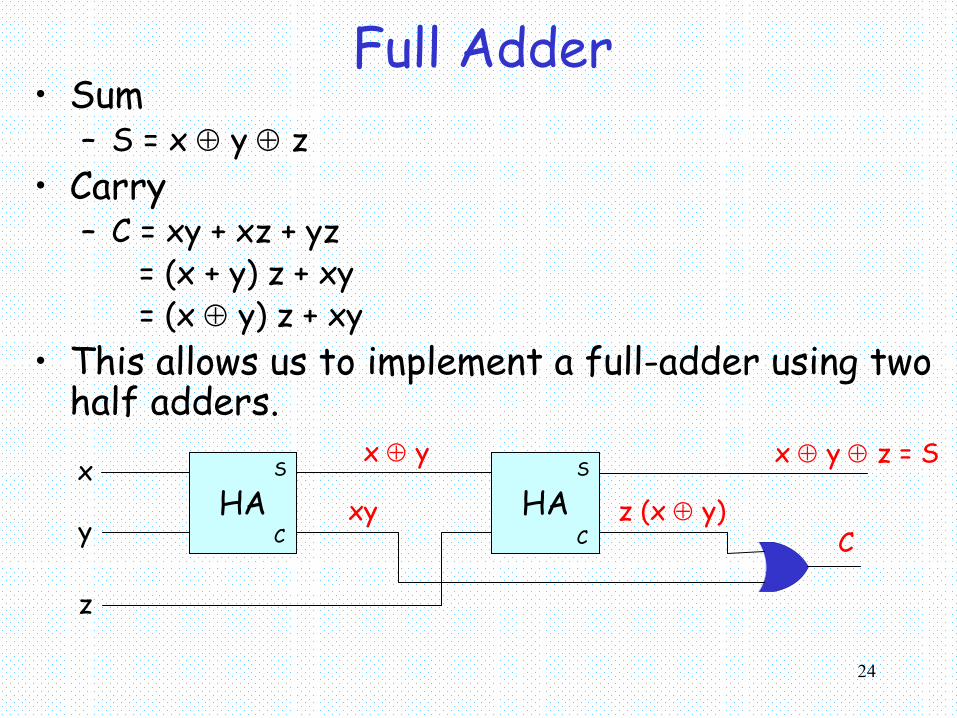
Full Adder• Sum
– S = x ⊕ y ⊕ z• Carry
– C = xy + xz + yz= (x + y) z + xy= (x ⊕ y) z + xy
• This allows us to implement a full-adder using two half adders.
x ⊕ y x ⊕ y ⊕ z = S
HA
z
S
Cz (x ⊕ y)HA
x
y
S
C Cxy

25
HAHA
Full Adder Using Half Adders
xy
C
S
z

26
Integer Addition• Binary adder:
– A digital circuit that produces the arithmetic sum of two binary numbers
– A = (an-1, an-2, …, a1, a0) – B = (bn-1, bn-2, …, b1, b0)
• A simple case: 4-bit binary adder
FAx y
zC
S
a0 b0
C0=0
S0
C1FAx y
zC
S
a1 b1
S1
C2FAx y
zC
S
a2 b2
S2
C3FAx y
zC
S
a3 b3
S3
C4
Ripple-carry adder

27
Hierarchical Design Methodology• The design methodology we used to build carry-
ripple adder is what is referred as hierarchical design.
• In classical design, we have to:– 9 inputs– 5 outputs– five truth tables with 29 = 512 entries each– We have to optimize five Boolean functions with 9
variables each.• Hierarchical design
– we divide our design into smaller functional blocks – connect functional units to produce the big
functionality

28
Carry Propagation• What is the total propagation time of 4-bit
ripple-carry adder ?– τFA: propagation time of a single full adder.– We have four full adders connected in cascaded
fashion– Total propagation time: 4τFA.
ai
bi
Ci+1
4τFA ≈ 8τXOR
Pi
Gi
Si
Ci

29
Faster Adders• The carry propagation technique is a limiting
factor in the speed with which two numbers are added.
• Two alternatives– use faster gates with reduced delays– Increase the circuit complexity (i.e. put more gates)
in such a way that the carry delay time is reduced.• An example for the latter type of solution is
carry lookahead adders– Two binary variables:
1. Pi = ai ⊕ bi – carry propagate2. Gi = aibi – carry generate
30
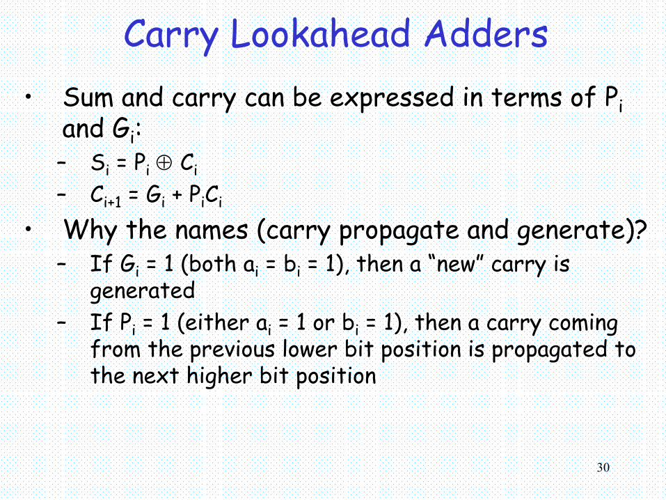
Carry Lookahead Adders• Sum and carry can be expressed in terms of Pi
and Gi:– Si = Pi ⊕ Ci
– Ci+1 = Gi + PiCi
• Why the names (carry propagate and generate)?– If Gi = 1 (both ai = bi = 1), then a “new” carry is
generated– If Pi = 1 (either ai = 1 or bi = 1), then a carry coming
from the previous lower bit position is propagated to the next higher bit position

31
4-bit Carry Lookahead Adder• We can use the carry propagate and carry
generate signals to compute carry bits used in addition operation– C0 = input– C1 = G0 + P0C0
– C2 = G1 + P1C1
= G1 + P1(G0 + P0C0) = G1 + P1G0 + P1P0C0
– C3 = G2 + P2C2 = G2 + P2(G1 + P1G0 + P1P0C0) = G2 + P2G1 + P2P1G0 + P2P1P0C0
– P0 = a0 ⊕ b0 and G0 = a0b0
– P1 = a1 ⊕ b1 and G1 = a1b1
– P2 = a2 ⊕ b2 and G2 = a2b2
– P3 = a3 ⊕ b3 and G3 = a3b3
32
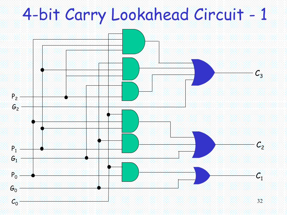
4-bit Carry Lookahead Circuit - 1
C1
G0
P0
C0
P1
G1
C2
P2
G2
C3
33
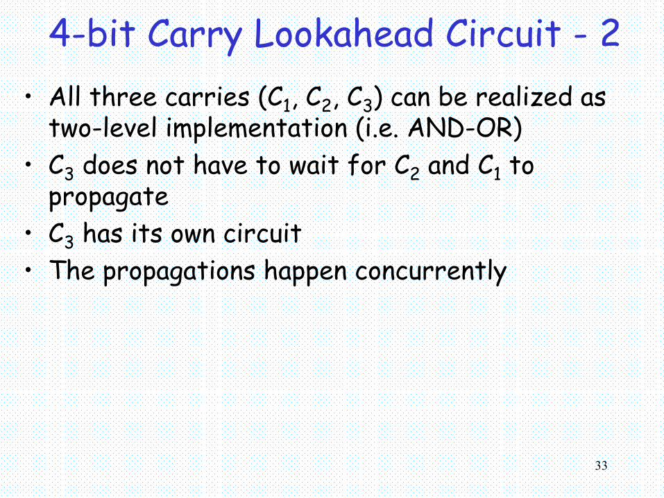
4-bit Carry Lookahead Circuit - 2• All three carries (C1, C2, C3) can be realized as
two-level implementation (i.e. AND-OR)• C3 does not have to wait for C2 and C1 to
propagate• C3 has its own circuit• The propagations happen concurrently
34
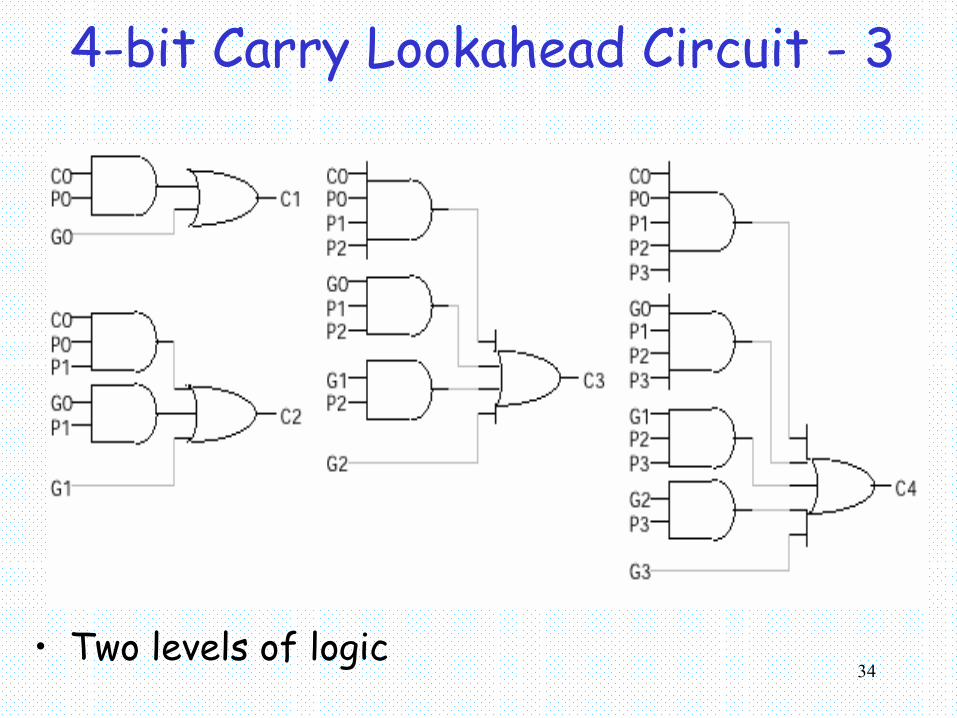
4-bit Carry Lookahead Circuit - 3
• Two levels of logic

35
4-bit Carry Lookahead Addera3b3
a2b2
a1b1
a0b0
C0
C4
P3
P2
S3
S2
P1 S1
P0 S0
Carry Lookahead
circuit
P3
G3
P2
G2
P0
G0
P1
G2
C0
C4
C3
C2
C1

36
Propagation Time of Carry Lookahead Adders
• Carry lookahead circuit has the delay of two gates– remember it has been implemented as two-level AND-
OR logic– To generate Pi and Gi we need one gate delay – To compute Si we need one gate delay– In total, overall delay is 4 gate delay.
• In general,– carry-ripple adders have O(n) gate delays– carry lookahead adders have O(log2n) gate delays
37
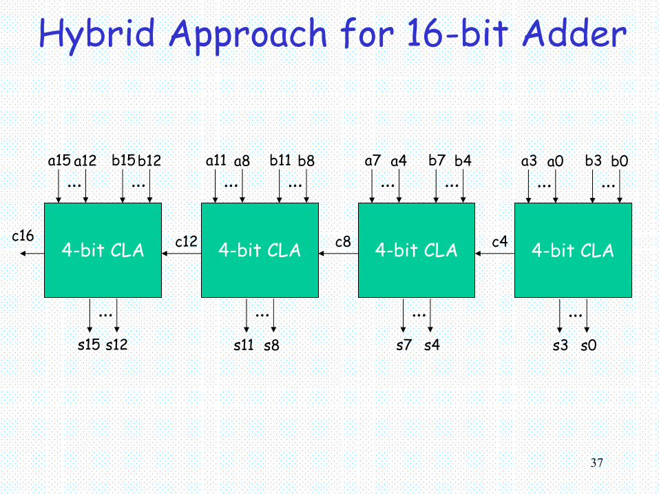
Hybrid Approach for 16-bit Adder
4-bit CLA
…b3 b0
…a3 a0
…s3 s0
c44-bit CLA
…b7 b4
…a7 a4
…s7 s4
c84-bit CLA
…b11 b8
…a11 a8
…
c12
s11 s8
4-bit CLA
…b15b12
…a15 a12
…s15 s12
c16

38
Subtractor• Recall how we do subtraction (2’s complement)
– A – B = A + (2n-1 – B)
4-bit adder circuit
a3 b3 a2 b2 a1 b1 a0 b0
C4 C0
S3 S2 S1 S0
a3 a2 a1 a0 logic-1b3 b2 b1 b0
S3 S2 S1 S0C4
39
Overflow• How to detect overflows:
– two n-bit numbers– we add(/subtract) them, and result may be a (n+1)-bit
number overflow.– Unsigned numbers:
• easy• check the carryout.
– Signed numbers • more complicated• overflow occurs in addition, when the operands are
of the same sign

40
Examples: Overflows• Example 1: 8-bit signed numbers
15911111001…009168
…00…00
1101101000100010
• Example 2: 8-bit signed numbers
-15910000110…11-91-68
…11…11
1010010100111101

41
How to Detect Overflows:• First Method
1. If both operands are positive and the MSB of the result is 1.
2. If both operands are negative and the MSB of the result is 0.
01111011010100010110001011000000VSn-1bn-1an-1
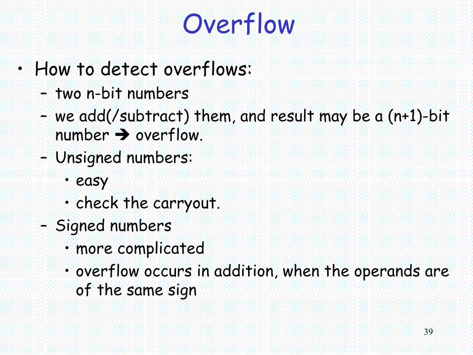
42
Detecting Overflows: First Method
• V = an-1’ bn-1’ Sn-1 + an-1 bn-1 Sn-1’
• Can we do it better?
10001
0010010110100
bn-1Sn-1an-1
43
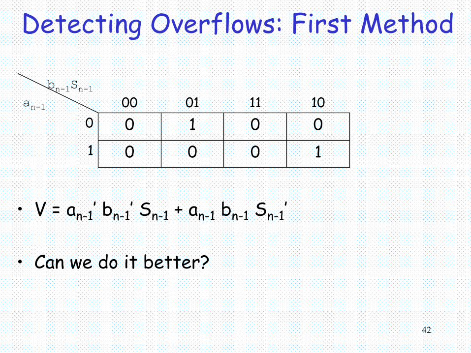
Detecting Overflows• Second method:
– Remember we have other variables when adding:• Carries
S11111001…00C000000010B11011010…00A00100010…00
S10000110…11C000111101B10100101…11A00111101…11
Look at C7and C8 in both cases
44
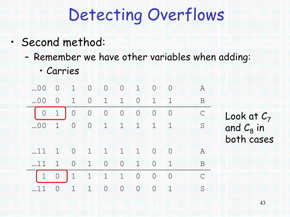
Detecting Overflows: Second Method
• Observations – Case 1: V = 1 when C7 = 1 and C8 = 0– Case 2: V = 1 when C7 = 0 and C8 = 1– V = C7 ⊕ C8 = 1– Think about whether this could happen when the
operands have different signs.• C7 = C8
• Overflow detection logic– Which one is simpler?– V = C7 ⊕ C8
– V = a7’ b7’ S7 + a7 b7 S7’
45
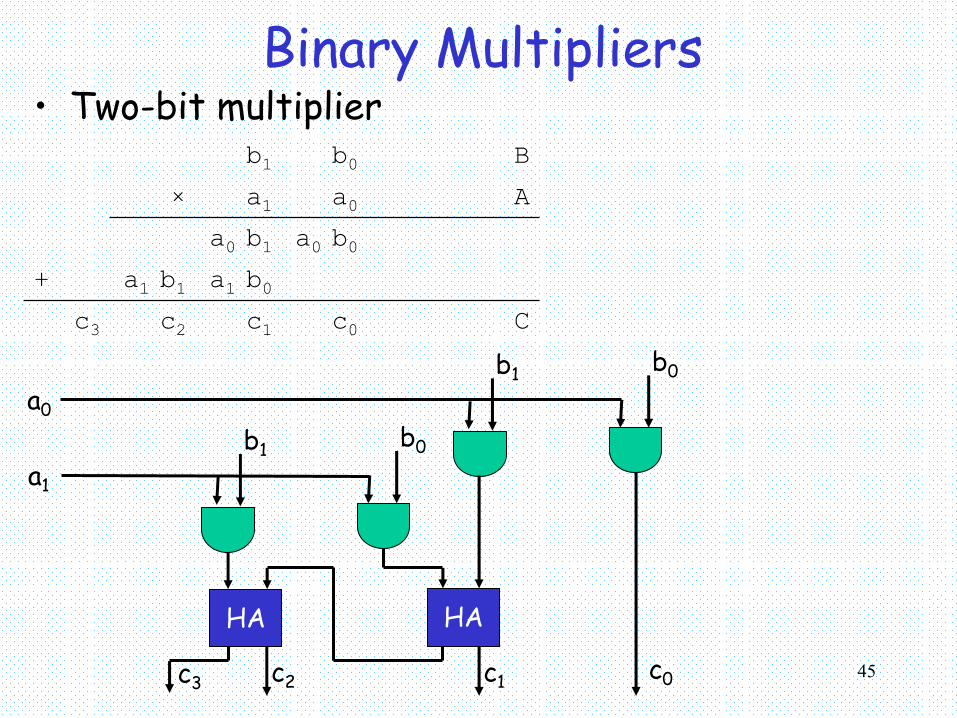
Binary Multipliers• Two-bit multiplier
Cc0c1c2c3a1 b0a1 b1+
a0 b0a0 b1Aa0a1×Bb0b1
b0b1a0
b0b1a1
c0
HA
c1
HA
c2c3
46
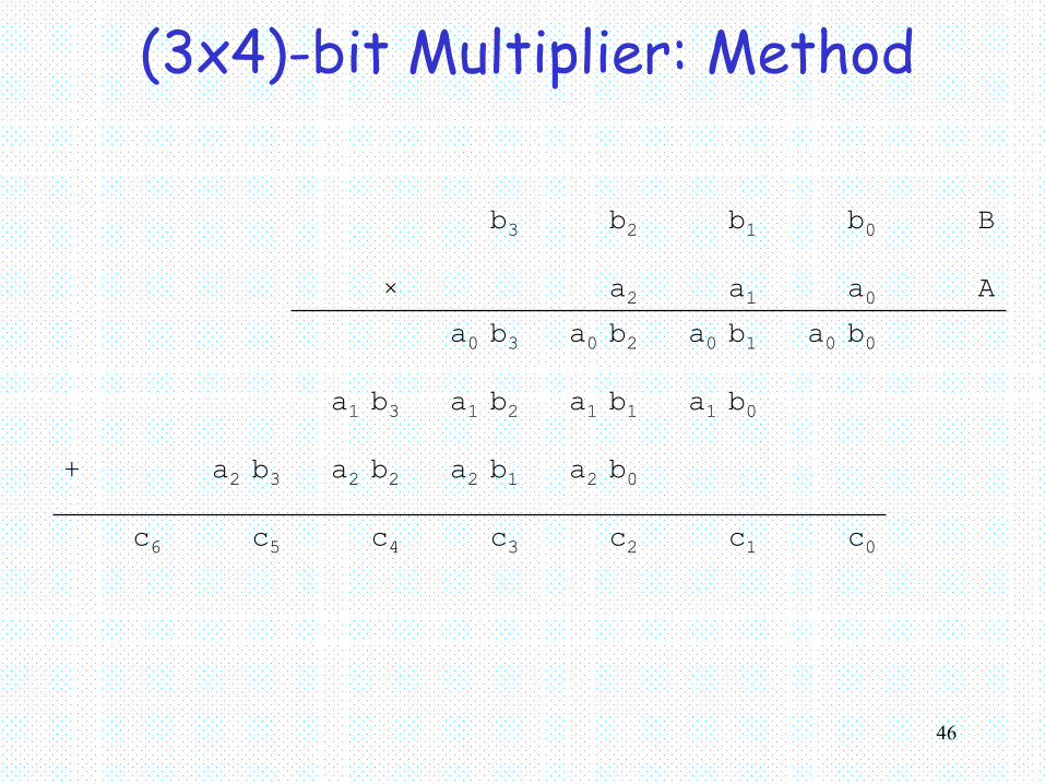
(3x4)-bit Multiplier: Method
c0c1c2c3c4c5c6
a2 b0a2 b1a2 b2a2 b3+
a1 b0a1 b1a1 b2a1 b3
a0 b0a0 b1a0 b2a0 b3Aa0a1a2×
Bb0b1b2b3
47
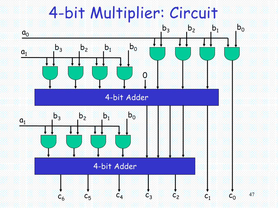
4-bit Multiplier: Circuitb0b1a0
b2b3
b0b1a1b2b3
b0b1a1b2b3
4-bit Adder
4-bit Adder
c0c1c2c3c4c5c6
0

48
mxn-bit Multipliers• Generalization:• multiplier: m-bit integer• multiplicand: n-bit integers• mxn AND gates• (m-1) adders
– each adder is n-bit

49
Magnitude Comparator • Comparison of two integers: A and B.
– A > B (1, 0, 0) = (x, y, z)– A = B (0, 1, 0) = (x, y, z)– A < B (0, 0, 1) = (x, y, z)
• Example: 4-bit magnitude comparator– A = (a3, a2, a1, a0) and B = (b3, b2, b1, b0) 1. (A=B) case
• they are equal if and only if ai = bi 0 ≤ i ≤ 3• ti = (ai ⊕ bi )’ 0 ≤ i ≤ 3• y = (A=B) = t3 t2 t1 t0

50
4-bit Magnitude Comparator 2. (A > B) and (A < B) cases
– We compare the most significant bits of A and B first.• if (a3 = 1 and b3 = 0) A > B• else if (a3 = 0 and b3 = 1) A < B• else (i.e. a3 = b3) compare a2 and b2.
x = (A>B) = a3 b3’ + t3 a2 b2’ + t3t2 a1 b1’ + t3t2t1 a0 b0’z = (A<B) = a3’ b3 + t3 a2’ b2 + t3t2 a1’ b1 + t3t2t1 a0’ b0
y = (A=B) = t3 t2 t1 t0
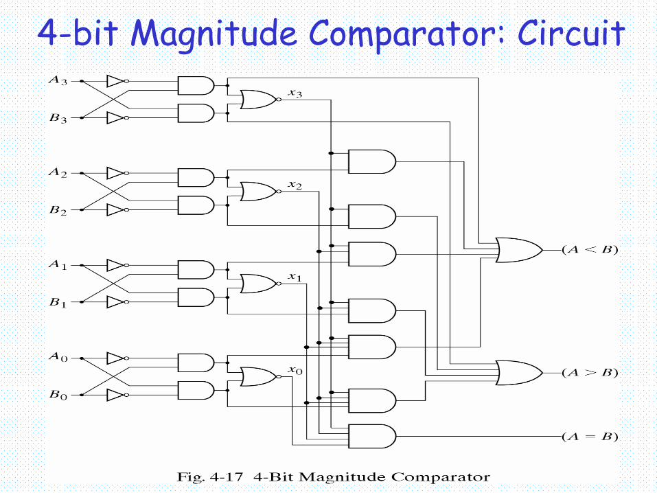
51
4-bit Magnitude Comparator: Circuit

52
Decoders• A binary code of n bits
– capable of representing 2n distinct elements of coded information
– A decoder is a combinational circuit that converts binary information from n binary inputs to a maximum of 2n unique output lines
2x4 decoder
x
y
d0
d1d2
d3 100011010001001010000100d3d2d1d0yx
• d0 = x’y’• d1 = x’y
• d2 = xy’• d3 = xy

53
2-to-4-Line Decoder• Some decoders are constructed with NAND
gates. – Thus, active output will be logic-0– They also include an “enable” input to control the
circuit operation
01111101011010110110011100001111XX1d3d2d1d0yxe
• d0 = e + x + y = (e’x’y’)’• d1 = e + x + y’ = (e’x’y)’• d2 = e + x’ + y = (e’xy’)’• d3 = e + x’ + y’ = (e’xy)’

54
2-to-4-Line Decoder with Enabled0 = e + x + y = (e’x’y’)’d1 = e + x + y’ = (e’x’y)’d2 = e + x’ + y = (e’xy’)’d3 = e + x’ + y’ = (e’xy)’
d0
d1
d2
d3
e
x
y
55
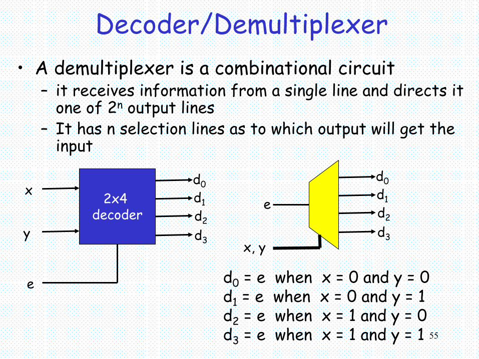
Decoder/Demultiplexer• A demultiplexer is a combinational circuit
– it receives information from a single line and directs it one of 2n output lines
– It has n selection lines as to which output will get the input
2x4 decoder
x
y
d0d1d2
d3
e
d0d1d2
d3
e
x, y
d0 = e when x = 0 and y = 0d1 = e when x = 0 and y = 1d2 = e when x = 1 and y = 0d3 = e when x = 1 and y = 1
56
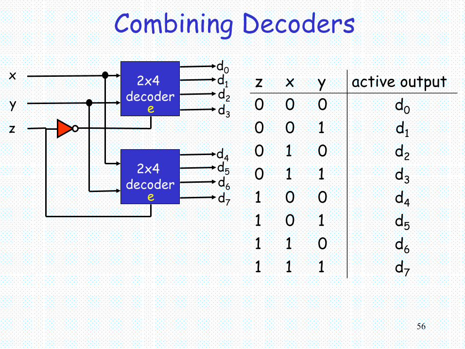
Combining Decoders
2x4 decoder
x
y
d0d1d2d3e
2x4 decoder
d4d5d6d7e
z
d7111d6011d5101d4001d3110d2010d1100d0000
active outputyxz

57
Decoder as a Building Block• A decoder provides the 2n minterms of n input
variable
2x4 decoder
x
y
d0 = x’y’d1 = x’yd2 = xy’d3 = xy
• We can use a decoder and OR gates to realize any Boolean function expressed as sum of minterms– Any circuit with n inputs and m outputs can be realized
using a n-to-2n-line encoder and m OR gates

58
Example: Decoder as a Building Block• Full adder
– C = xy + xz + yz = Σ(3, 5, 6, 7)– S = x ⊕ y ⊕ z = Σ(1, 2, 4, 7)
3x8 decoder
x
y
z
01234567
S
C

59
Encoders• An encoder is a combinational circuit that
performs the inverse operation of a decoder– number of inputs: 2n
– number of outputs: n– the output lines generate the binary code
corresponding to the input value• Example: n = 2
111000010100100010000001
yxd3d2d1d0

60
Priority Encoder• Problem with a regular encoder:
– only one input can be active at any given time– the output is undefined for the case when more than
one input is active simultaneously.• Priority encoder:
– there is a priority among the inputs
1111XXX
10101XX
110001X
1000001
0XX0000
Vyxd3d2d1d0
61
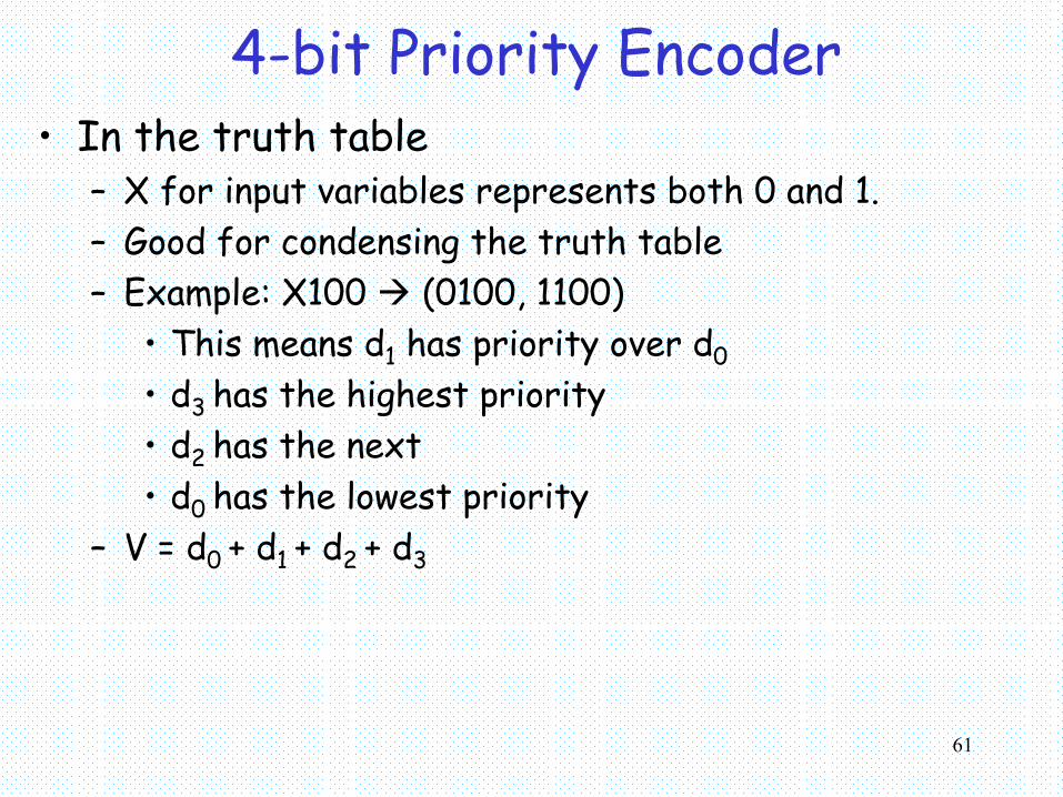
4-bit Priority Encoder• In the truth table
– X for input variables represents both 0 and 1. – Good for condensing the truth table– Example: X100 (0100, 1100)
• This means d1 has priority over d0
• d3 has the highest priority• d2 has the next• d0 has the lowest priority
– V = d0 + d1 + d2 + d3
62
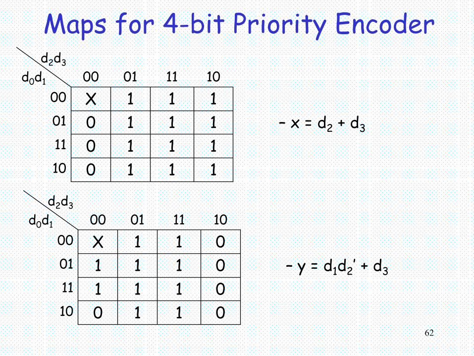
Maps for 4-bit Priority Encoder
111010111011111001111X0010110100
d2d3
d0d1
– x = d2 + d3
011010011111011101011X0010110100
d2d3
d0d1
– y = d1d2’ + d3
63
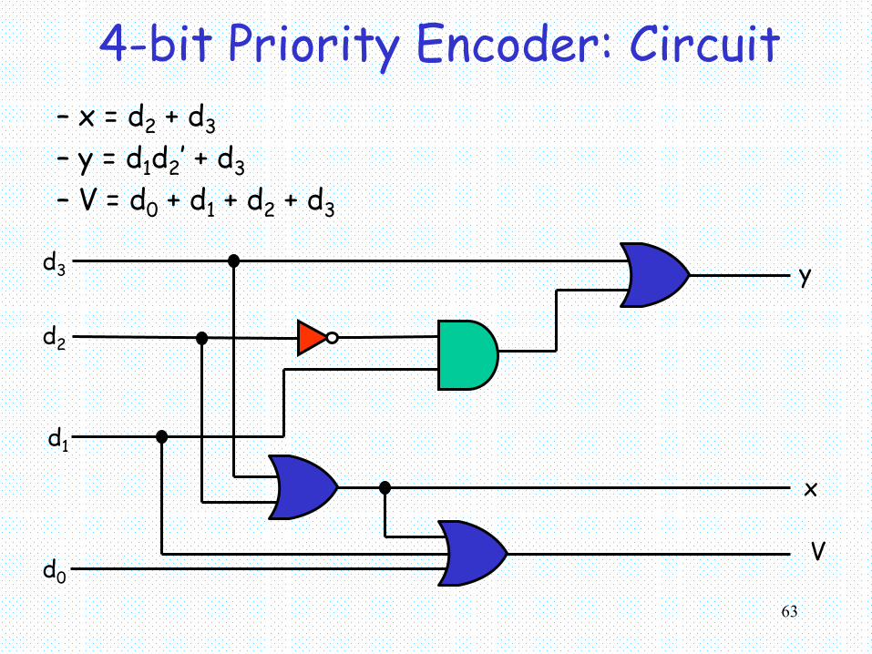
4-bit Priority Encoder: Circuit
d0
d1
d2
d3 y
x
V
– x = d2 + d3
– y = d1d2’ + d3
– V = d0 + d1 + d2 + d3
64
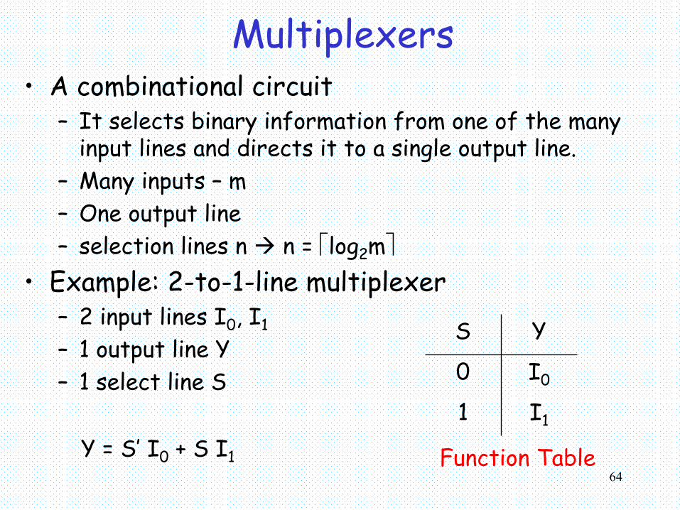
Multiplexers• A combinational circuit
– It selects binary information from one of the many input lines and directs it to a single output line.
– Many inputs – m– One output line– selection lines n n = log2m
• Example: 2-to-1-line multiplexer– 2 input lines I0, I1
– 1 output line Y– 1 select line S
I11
I00
YS
Y = S’ I0 + S I1 Function Table

65
2-to-1-Line Multiplexer
• Special Symbol
SI0
Y
I1
Y = S’ I0 + S I1
I0
I1
MUX Y
S
0
1

66
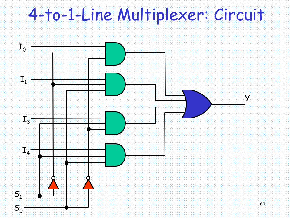
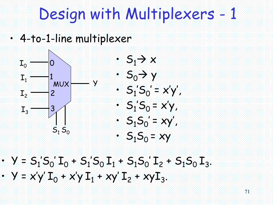
4-to-1-Line Multiplexer• 4 input lines: I0, I1, I2, I3• 1 output line: Y• 2 select lines: S0, S1.
I311I201I110I000YS1S0 Y = S0’S1’I0 + S0’S1I1 + S0S1’I2 + S0S1I3
Interpretation:• In case S0 = 0 and S1 = 0, Y selects I0
• In case S0 = 0 and S1 = 1, Y selects I1
• In case S0 = 1 and S1 = 0, Y selects I2
• In case S0 = 1 and S1 = 1, Y selects I3
67
4-to-1-Line Multiplexer: Circuit
S0
I0
Y
I1
I3
I4
S1
68
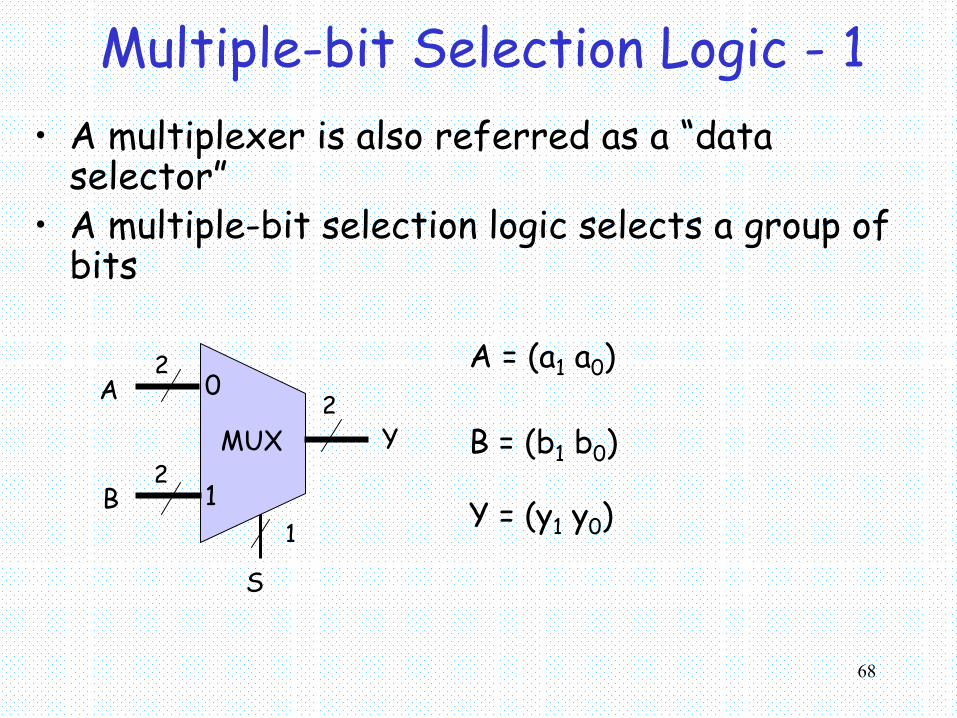
Multiple-bit Selection Logic - 1• A multiplexer is also referred as a “data
selector”• A multiple-bit selection logic selects a group of
bits
A
B
MUX Y
S
0
1
2
2
2
1
A = (a1 a0)
B = (b1 b0)
Y = (y1 y0)

69
Multiple-bit Selection Logic - 2
S
a1
b1
MUX y1
0
1
a0
b0
MUX y0
0
1
E
B10A00
all 0’s X1YSE

70
Design with Multiplexers - 1• Reminder: design with decoders
• Half adder– C = xy = Σ(3)– S = x ⊕ y = x’y + xy’ + Σ(1, 2)
2x4 decoder
x
y
0
1
2
3
S
C
• A closer look will reveal that a multiplexer is nothing but a decoder with OR gates
71
Design with Multiplexers - 1• 4-to-1-line multiplexer
I0
I1 MUX Y
S1
0
1
I2
I3
2
3
S0
• Y = S1’S0’ I0 + S1’S0 I1 + S1S0’ I2 + S1S0 I3.• Y = x’y’ I0 + x’y I1 + xy’ I2 + xyI3.
• S1 x• S0 y• S1’S0’ = x’y’, • S1’S0 = x’y,• S1S0’ = xy’, • S1S0 = xy

72
Example: Design with Multiplexers• Example: S = Σ(1, 2)
I0
I1 MUX Y
S1
0
1
I2
I3
2
3
S0
0 =
1 =
1 =
0 =
x y
= xy’ + x’y

73
Design with Multiplexers Efficiently• More efficient way to implement a n-variable
Boolean function1. Use a multiplexer with n-1 selection inputs2. First (n-1) variables are connected to the selection
inputs3. The remaining variable is connected to data inputs
• Example: S = Σ(1, 2)
y = I0
y’ = I1
Y = S’ I0 + S I1MUX0
1
x
Y = x’y + xy’
74
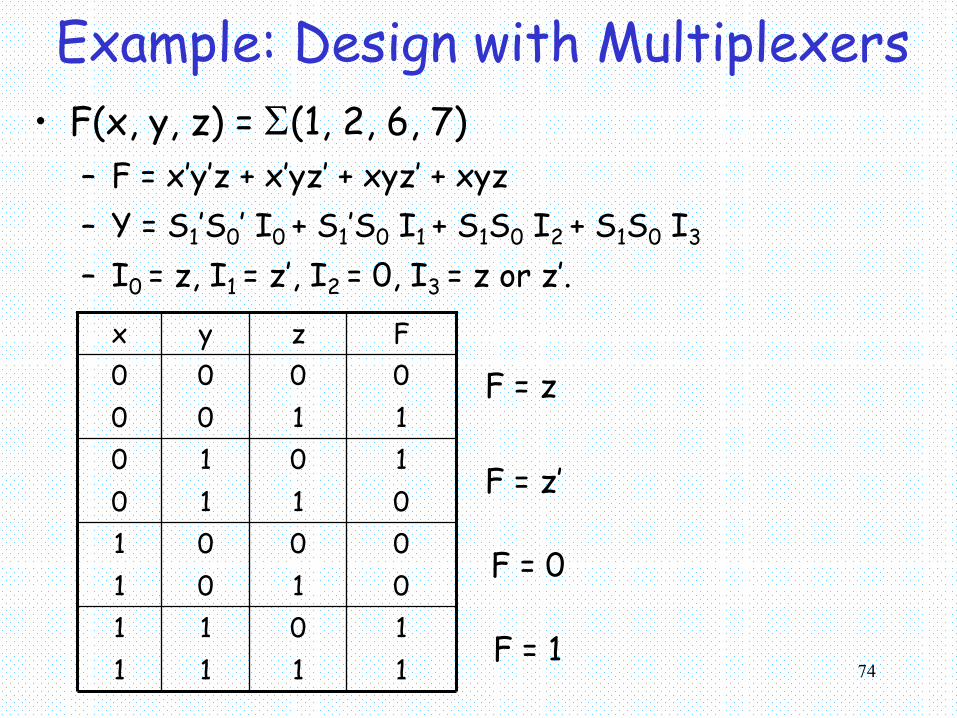
Example: Design with Multiplexers• F(x, y, z) = Σ(1, 2, 6, 7)
– F = x’y’z + x’yz’ + xyz’ + xyz– Y = S1’S0’ I0 + S1’S0 I1 + S1S0 I2 + S1S0 I3
– I0 = z, I1 = z’, I2 = 0, I3 = z or z’.
11111011010100010110101011000000Fzyx
F = z
F = z’
F = 0
F = 1

75
Example: Design with Multiplexers
z
z’
0
1
MUX
0
1
2
3
x y
F = x’y’z + x’yz’ + xy
F = x’y’z + x’yz’ + xyz’ + xyz F = z when x = 0 and y = 0F = z’ when x = 0 and y = 1F = 0 when x = 1 and y = 0F = 1 when x = 1 and y = 1

76
Design with Multiplexers• General procedure for n-variable Boolean
function– F(x1, x2, ..., xn)
1. The Boolean function is expressed in a truth table2. The first (n-1) variables are applied to the selection
inputs of the multiplexer (x1, x2, ..., xn-1)3. For each combination of these (n-1) variables,
evaluate the value of the output as a function of the last variable, xn.
• 0, 1, xn, xn’ 4. These values are applied to the data inputs in the
proper order.

77
Combining Multiplexers
MUX
0
1
2
3
MUX
0
1
2
3
x y
x y
MUX0
1
z
I0
I2
I4
I6
I1
I3
I5
I7

78
Three-State Buffers• A different type of logic gate
– Instead of two states (i.e. 0, 1), it exhibits three states (0, 1, Z)
– Z (Hi-Z) is called high-impedance– When in Hi-Z state the circuit behaves like an open
circuit (the output appears to be disconnected, and the circuit has no logic significance)
A
C
Y = A if C =1Y = Hi-Z if C = 0
input
controlinput

79
3-State Buffers• We can connect the outputs of three-state
buffers– provided that no two three-state buffers drive the
line to opposite 0 and 1 values at the same time.– Remember we cannot connect the outputs of other
logic gates.
111
001
Hi-ZX0
YAC
80
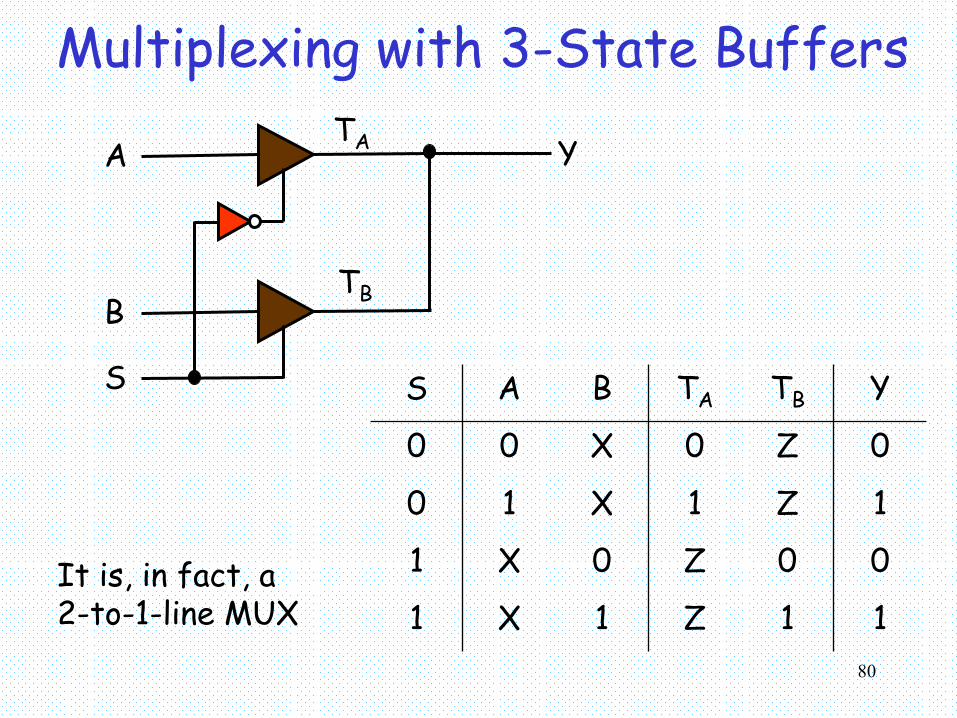
Multiplexing with 3-State Buffers
A
S
B
TA
TB
Y
11Z1X1
00Z0X1
1Z1X10
0Z0X00
YTBTABAS
It is, in fact, a 2-to-1-line MUX

81
Two Active Outputs - 1
A
C1
B
TA
TB
YC0
What will happen if C1 = C0 = 1?
1111100011
10110111
YBAC0C1
ZXX00
11X0100X011X1100X010

82
Design Principle with 3-State Buffers
• Designer must be sure that only one control input must be active at a time.– Otherwise the circuit may be destroyed by the large
amount of current flowing from the buffer output at logic-1 to the buffer output at logic-0.
2x4 decoder
S1
S0
E
x
y
w
z
t
83
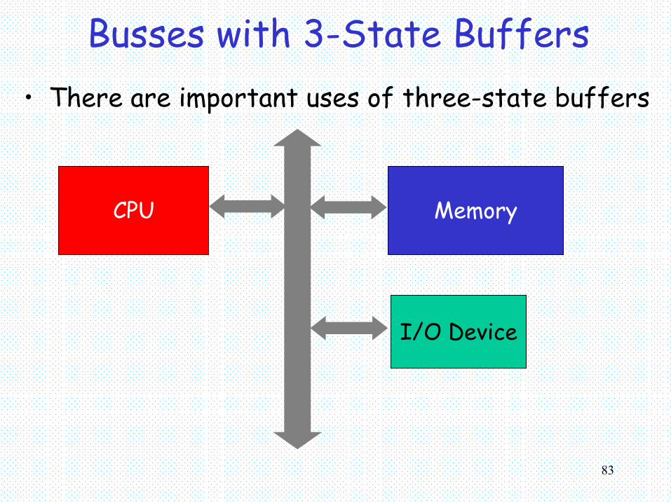
Busses with 3-State Buffers• There are important uses of three-state buffers
CPU Memory
I/O Device


