Type Ordering Code Package TLE 7273 GV50 SP000067155 P-DSO-14-8 * TLE 7273 GV33 Q67006-A9686 P-DSO-14-8 * TLE 7273 GV26 Q67006-A9685 P-DSO-14-8 Low Drop Voltage Regulator TLE 7273 P-DSO-14-3, -8, -9, -11, 14 Final-/ *Target Data Sheet 1 Rev. 1.0, 2005-11-30 Features • Output voltage 5 V, 3.3 V or 2.6 V • Output voltage tolerance ±2% up to I Q =180mA • Ultra low quiescent current consumption < 35 µA • Inhibit function • Very low dropout voltage • Reset with adjustable power-on delay • Window watchdog with current dependent deactivation • Output protected against short circuit • Wide operation range: up to 45 V • Wide temperature range: -40 °C to 150 °C • Overtemperature Shutdown Functional Description The TLE 7273 is a monolithic integrated voltage regulator with integrated window watchdog and reset dedicated for microcontroller supplies under harsh automotive environment conditions. Due to its ultra low quiescent current, the TLE 7273 is perfectly suited for applications that are permanently connected to battery. In addition, the regulator can be shut down via the Inhibit input causing the current consumption to drop below 3 µA. The TLE 7273 is equipped with protection functions against overload, short circuit and overtemperature. It operates in the wide junction temperature range from -40 °C to 150 °C. Derivatives market with “*” have “Target” Status, others have “Final” Status
Transcript
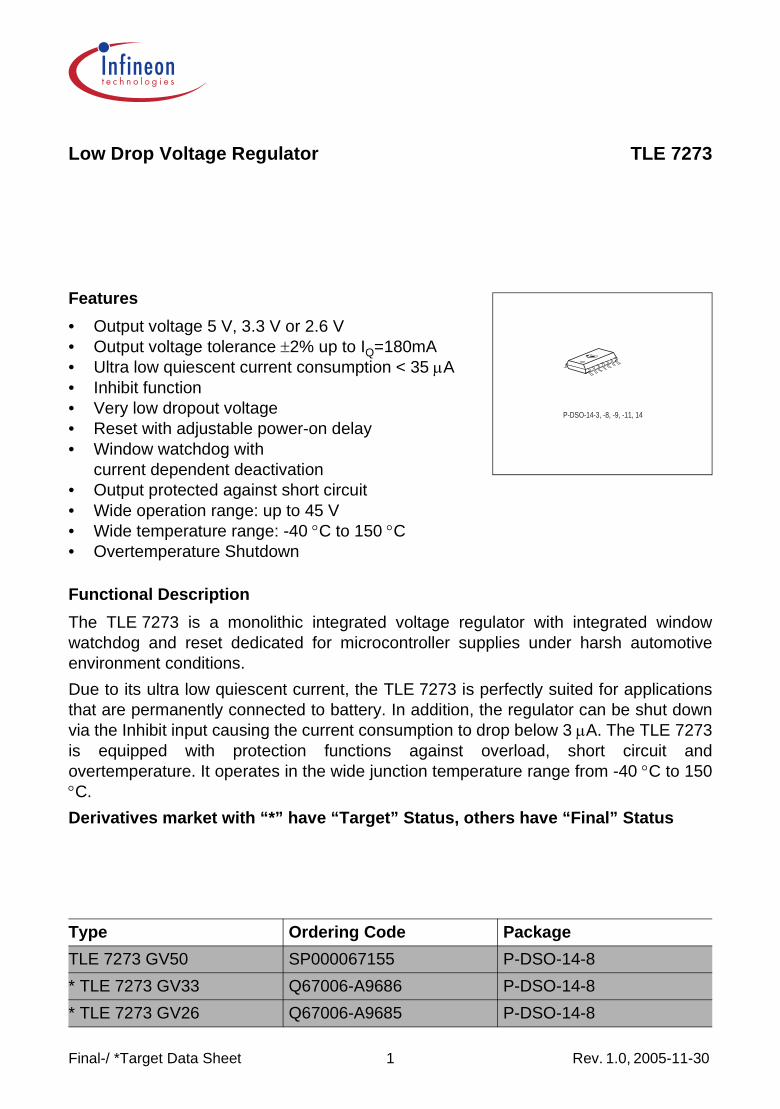
Low Drop Voltage Regulator TLE 7273
P-DSO-14-3, -8, -9, -11, 14
Features
• Output voltage 5 V, 3.3 V or 2.6 V• Output voltage tolerance ±2% up to IQ=180mA• Ultra low quiescent current consumption < 35 µA• Inhibit function• Very low dropout voltage• Reset with adjustable power-on delay• Window watchdog with
current dependent deactivation• Output protected against short circuit• Wide operation range: up to 45 V• Wide temperature range: -40 °C to 150 °C• Overtemperature Shutdown
Functional Description
The TLE 7273 is a monolithic integrated voltage regulator with integrated window watchdog and reset dedicated for microcontroller supplies under harsh automotive environment conditions.
Due to its ultra low quiescent current, the TLE 7273 is perfectly suited for applications that are permanently connected to battery. In addition, the regulator can be shut down via the Inhibit input causing the current consumption to drop below 3 µA. The TLE 7273is equipped with protection functions against overload, short circuit and overtemperature. It operates in the wide junction temperature range from -40 °C to 150 °C.
Derivatives market with “*” have “Target” Status, others have “Final” Status
Type Ordering Code Package
TLE 7273 GV50 SP000067155 P-DSO-14-8
* TLE 7273 GV33 Q67006-A9686 P-DSO-14-8
* TLE 7273 GV26 Q67006-A9685 P-DSO-14-8
Final-/ *Target Data Sheet 1 Rev. 1.0, 2005-11-30
TLE 7273
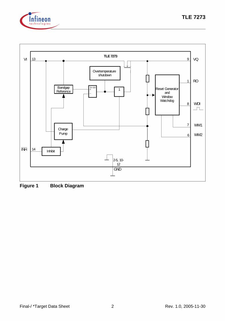
Figure 1 Block Diagram
WDI
WM1
Reset Generatorand
WindowWatchdog
Inhibit
ChargePump
TLE 7273
Overtemperatureshutdown
BandgapReference 1
INH
9 VQ
RO
WM2
VI
14
13
1
8
7
6
2-5, 10-12
GND
Final-/ *Target Data Sheet 2 Rev. 1.0, 2005-11-30
TLE 7273
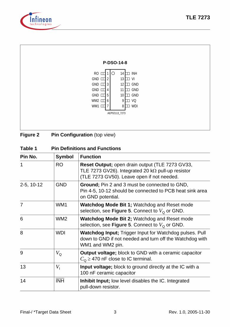
Figure 2 Pin Configuration (top view)
Table 1 Pin Definitions and Functions
Pin No. Symbol Function
1 RO Reset Output; open drain output (TLE 7273 GV33, TLE 7273 GV26). Integrated 20 kΩ pull-up resistor (TLE 7273 GV50). Leave open if not needed.
2-5, 10-12 GND Ground; Pin 2 and 3 must be connected to GND,Pin 4-5, 10-12 should be connected to PCB heat sink area on GND potential.
7 WM1 Watchdog Mode Bit 1; Watchdog and Reset mode selection, see Figure 5. Connect to VQ or GND.
6 WM2 Watchdog Mode Bit 2; Watchdog and Reset mode selection, see Figure 5. Connect to VQ or GND.
8 WDI Watchdog Input; Trigger Input for Watchdog pulses. Pull down to GND if not needed and turn off the Watchdog with WM1 and WM2 pin.
9 VQ Output voltage; block to GND with a ceramic capacitor CQ ≥ 470 nF close to IC terminal.
13 VI Input voltage; block to ground directly at the IC with a 100 nF ceramic capacitor
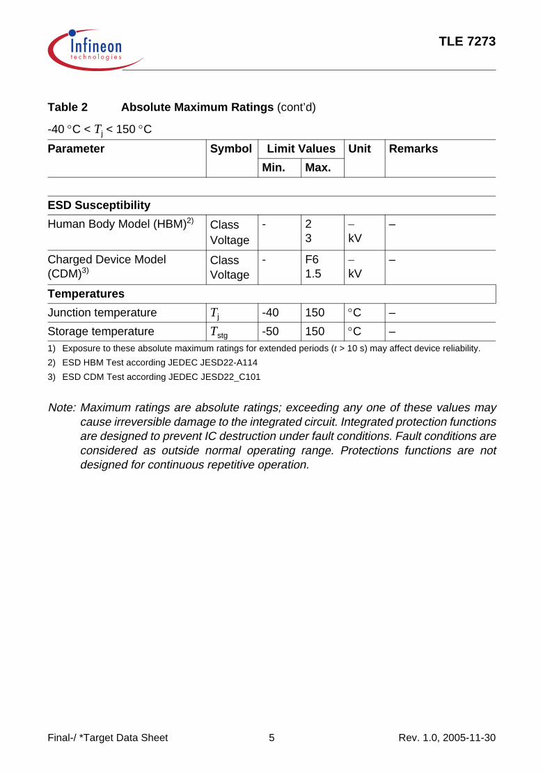
Note: Maximum ratings are absolute ratings; exceeding any one of these values may cause irreversible damage to the integrated circuit. Integrated protection functions are designed to prevent IC destruction under fault conditions. Fault conditions are considered as outside normal operating range. Protections functions are not designed for continuous repetitive operation.
ESD Susceptibility
Human Body Model (HBM)2) ClassVoltage
- 23
−kV
–
Charged Device Model (CDM)3)
ClassVoltage
- F61.5
−kV
–
Temperatures
Junction temperature Tj -40 150 °C –
Storage temperature Tstg -50 150 °C –1) Exposure to these absolute maximum ratings for extended periods (t > 10 s) may affect device reliability.
2) ESD HBM Test according JEDEC JESD22-A114
3) ESD CDM Test according JEDEC JESD22_C101
Table 2 Absolute Maximum Ratings (cont’d)
-40 °C < Tj < 150 °C
Parameter Symbol Limit Values Unit Remarks
Min. Max.
Final-/ *Target Data Sheet 5 Rev. 1.0, 2005-11-30
TLE 7273
Note: In the operating range the functions given in the circuit description are fulfilled.
Table 3 Operating Range
Parameter Symbol Limit Values Unit Remarks
Min. Max.
Input voltage VI 5.5 45 V TLE 7273 GV50
4.2 45 V TLE 7273 GV33
4.2 45 V TLE 7273 GV26
Junction temperature Tj -40 150 °C –
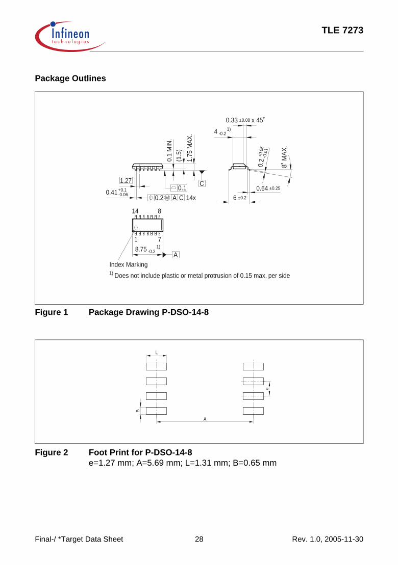
Thermal Resistances P-DSO-14-8
Parameter Symbol Limit Values Unit Remarks
typ.. max.
Junction pin Rthj-pin – 25 K/W Measure to pin 4
Junction ambient Rthj-a 130 – K/W PCB, only Footprint1)
Ignore window time tIW 25.6 32.0 38.4 ms Fast watchdog timing
51.2 64.0 76.8 ms Slow watchdog timing
Open window time tOW 25.6 32.0 38.4 ms Fast watchdog timing
51.2 64.0 76.8 ms Slow watchdog timing
Closed window time tCW 25.6 32.0 38.4 ms Fast watchdog timing
51.2 64.0 76.8 ms Slow watchdog timing
Window watchdog trigger time2)
tWD – 48 – ms Fast watchdog timing
– 96 – ms Slow watchdog timing
Watchdog deactivation current threshold
IQ,WD_off 0.50 1.50 5 mA IQ decreasingVI > 5.5V for TLE 7273 GV50VI > 4.2V for TLE 7273 GV33, TLE 7273 GV26
Electrical Characteristics (cont’d)
VI =13.5 V; – 40 °C < Tj < 150 °C; unless otherwise specified
Parameter Symbol Limit Values Unit Test Condition
min. typ. max.
Final-/ *Target Data Sheet 9 Rev. 1.0, 2005-11-30
TLE 7273
Watchdog activating current threshold
IQ,WD_on 0.50 1.70 5 mA IQ increasingVI > 5.5V for TLE 7273 GV50VI > 4.2V for TLE 7273 GV33, TLE 7273 GV26
Reset Output RO
Output Voltage Reset Switching Threshold
VRT 4.50 4.60 4.70 V TLE 7273 GV50VQ decreasing
3.00 3.07 3.13 V TLE 7273 GV333)
VI>4.2V, VQ decreasing
2.35 2.38 2.45 V TLE 7273 GV263)
VI>4.2V, VQ decreasing
Input Voltage Reset Switching Threshold
VRT_VI – 3.9 4.0 V TLE 7273 GV263)
TLE 7273 GV333)
VQ>VRT, VI decreasing
Output Voltage Reset Hysteresis
VRH – 45 – mV TLE 7273 GV26
– 60 – mV TLE 7273 GV33
– 90 – mV TLE 7273 GV50
Reset sink current IRO 1.75 – – mA TLE 7273 GV50VQ=4.5V,VRO=0.25V
1.30 – – mA TLE 7273 GV33VQ=3.0V,VRO=0.25V
1.10 – – mA TLE 7273 GV26VQ=2.35V,VRO=0.25V
Reset output low voltage
VROL – 0.15 0.25 V VQ ≥ 1 V;IRO < 200 µA
Reset high voltage VROH 4.5 – – V TLE 7273 GV50
Reset high leakage current
IROLK – – 1 µA TLE 7273 GV33TLE 7273 GV26
Electrical Characteristics (cont’d)
VI =13.5 V; – 40 °C < Tj < 150 °C; unless otherwise specified
Parameter Symbol Limit Values Unit Test Condition
min. typ. max.
Final-/ *Target Data Sheet 10 Rev. 1.0, 2005-11-30
TLE 7273
Integrated reset pull up resistor
RRO 10 20 40 kΩ TLE 7273 GV50Internally connected to VQ
Power-on Reset delay time
TRD 12.8 16.0 19.2 ms Fast reset timing
25.6 32.0 38.4 ms Slow reset timing
Reset Reaction Time
TRR - 4 12 µs
1) measured when the output voltage has dropped 100 mV from the nominal Value obtained at VI=13.5V.2) Recommendation for typical trigger time. tWD=tCW+1/2*tOW3) Reset Output triggered when Output Voltage VQ is lower than Output Voltage Reset Switching Threshold VRT
or is also triggered, when Input Voltage is decreasing to VI<4.0V and VQ>VRT
Electrical Characteristics (cont’d)
VI =13.5 V; – 40 °C < Tj < 150 °C; unless otherwise specified
Parameter Symbol Limit Values Unit Test Condition
min. typ. max.
Final-/ *Target Data Sheet 11 Rev. 1.0, 2005-11-30
TLE 7273
Circuit Description
Power On Reset and Reset Output
For an output voltage level of VQ ≥ 1 V, the reset output is held low. When the level of VQreaches the reset threshold VRT, the signal at RO remains low for the power-up reset delay time TRD. The reset function and timing is illustrated in Figure 3. The reset reaction time TRR avoids wrong triggering caused by short “glitches” on the VQ-line. In case of VQ power down (VQ < VRT for t > TRR) a logic low signal is generated at the pin RO to reset an external microcontroller.
The TLE 7273 GV50 features an integrated pull-up resistor on the reset output while the TLE 7273 GV33 and TLE 7273 GV26 have an open drain output requiring an external pull-up resistor ≥ 5.6 kΩ1). At low output voltage levels VQ < 1 V the integrated pull-up resistor of the TLE 7273 GV50 is switched off setting the reset output high ohmic. Example: Calculation based on the reset sink current and an external pull-up resistor connection to 5V:
Final-/ *Target Data Sheet 12 Rev. 1.0, 2005-11-30
TLE 7273
Application Circiut
Figure 4 Application Diagram
A typical application of the TLE 7273 is shown in Fig.4. To prevent the regulation loop from oscillating a ceramic capacitor ≥ 470nF is required at the output VQ. In contrast to most low drop voltage regulators, the TLE 7273 only needs moderate capacitance at the output and tolerates ceramic capacitors to keep the stability. This offers more design flexibility to the circuit designer enabling also to operate the device without tantalum capacitors.
Additionally, a blocking capacitor CB of 10 … 47 µF should be used for the output VQ to suppress influences from load surges to the voltage levels. This one can either be an aluminum electrolytic capacitor or a tantalum capacitor following the application requirements.
A general recommendation at Tj<90°C is to keep the drop over the equivalent serial resistor (ESR) of the blocking capacitor CB together with the discharge of the blocking
capacitor below 300mV. Since the regulator output current roughly rises linearly with time the discharge of the capacitor can be calculated as:
dVCB = dIQ*dt/CB
WDI
Vbatt
47µF 100nF
E.g. ingnition
100kOhm
E.g.Mircro
Controller
CB47µF
CQ470nF
5.6kOhm
TLE71273 Application Circuit
WM1
Reset Generatorand
WindowWatchdog
Inhibit
ChargePump
TLE 7273
Overtemperatureshutdown
BandgapReference 1
INH
9 VQ
RO
WM2
VI
14
13
1
8
7
6
2-5, 10-12
GND
Final-/ *Target Data Sheet 13 Rev. 1.0, 2005-11-30
TLE 7273
The drop across the ESR calculates as:dVESR = dI*ESR
To prevent a reset the following relationship must be fullfilled:dVC + dVESR < 300mV
Example: Assuming a load current step of dIQ = 50mA, a blocking capacitor of CQ =
22µF and a typical regulator reaction time under normal operating conditions of dt ~ 25µs and for special dynamic load conditions, such as load step from very low base load, a reaction time of dt ~ 75µs. For this expample the typical condition is considered and the calculation is done based on dt = 25µs:
dVC = 0.1A * 25µs/22µF = 114mV
So for the ESR we can allowdVESR = 300mV - 114mV = 186mV
The permissible ESR becomes:ESR = 186mV/100mA = 1.86Ohm
During design-in of the TLE7273 product family, special care needs to be taken with regards to the regulators reaction time on sudden load current changes starting from very low pre-load as well as cyclic load changes. The application note “TLE7x Voltage Regulators - Application Note about Transient Response at ultra low quiescent current Voltage Regulators” (see 3_cip05405.pdf) gives important hints for successful design-in of the Voltage Regulators of the TLE7x family.
Final-/ *Target Data Sheet 14 Rev. 1.0, 2005-11-30
TLE 7273
Watchdog Operation
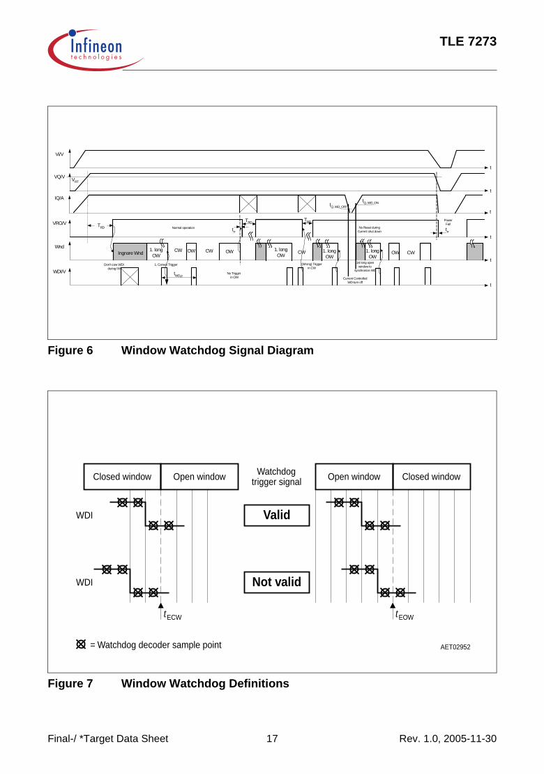
The watchdog uses a fraction of the charge pump oscillator’s clock signal as timebase. The watchdog timebase can be adjusted using the pins WM1 and WM2 (see Figure 5). The watchdog can be turned off setting WM1 and WM2 to high level. The timing values refer to typ. values with WM1 and WM2 connected to GND (fast watchdog and reset timing).
Figure 5 shows the state diagram of the window watchdog (WWD) and the watchdog and reset mode selection. After power-on, the reset output signal at the RO pin (microcontroller reset) is kept LOW for the reset delay time TRD of typ. 16 ms. With the LOW to HIGH transition of the signal at RO the device starts the ignore window time tCW(32 ms). During this window the signal at the WDI pin is ignored. Next the WWD starts the open window which is in the very first turn after power up a long open window with tmax = 4 * tOW. In the following turns, the timing corresponds to the standard timing setting as described in the specification.
When a valid trigger signal is detected during the open window a closed window is initialized immediately. A trigger signal within the closed window is interpreted as a pretrigger failure and results in a reset. After the closed window the open window with the duration tOW is started again. The open window lasts at minimum until the trigger process has occurred, at maximum tOW is 32 ms (typ. value with fast timing). A HIGH to LOW transition of the watchdog trigger signal at pin WDI is considerede as a valid trigger pulse.
See Figure 7: To avoid wrong triggering due to parasitic glitches two HIGH samples followed by two LOW samples (sample period tsam typ. 0.5 ms) are decoded as a valid trigger .
A reset is generated (RO goes LOW) if there is no trigger pulse during the open window or if a pretrigger occurs during the closed window. The triggering is correct also, if the first three samples (two HIGH one LOW) of the trigger pulse at pin WDI are inside the closed window and only the fourth sample (the second LOW sample) is taken in the open window.
After turning OFF the Watchdog by output current reduction, RO remains high. (see also the signal diagram in Figure 6). After turning ON the WWD again by exceeding the current threshold, the logic cycle starts again with the Ignore Window and goes then into the “1st. long open window”. This 1st long OW is maximum 4 * tOW long and allows the re-synchronisation between the micro controller and the WWD timing. The 1st. long OW is closed by the first valid trigger on WDI from the mirco controller. This trigger ensures the synchronisation. As soon as this trigger is done, the micro controller timing must be stable and correspondent to tWD .
Final-/ *Target Data Sheet 15 Rev. 1.0, 2005-11-30
TLE 7273
Figure 5 Window Watchdog State Diagram, Watchdog and Reset Modes
AEA03527_1.VSD
No Trigger
ClosedWindow
OpenWindow
Trigger
WM1 L L H H
WM2 L H L H
Window Watchdog Mode Fast Slow Fast Off
ResetTrigger
IgnoreWindow
Always
Always
No Trigger DuringOpen Window
Trigger DuringClosed Window
Reset Mode Fast Slow Slow Slow
WatchdogOFF
IQ > 5mA
AlwaysIQ < 0.5mA
Final-/ *Target Data Sheet 16 Rev. 1.0, 2005-11-30
TLE 7273
Figure 6 Window Watchdog Signal Diagram
Figure 7 Window Watchdog Definitions
t
Vi/V
VQ/V
VRO/V
Wnd
WDI/V
TRD
Ingnore Wnd
VRT
1. Correct Trigger
No Trigger in OW
trr
t
t
t
t
OWCW
trr
CW
(Wrong) Triggerin CW
tWD,p
1. longOW
1. longOW
1. longOW
TRDPowerFail
IQ/A
tTRD
OW CW
IQ, WD_ON
1. longOW
IQ, WD_OFF
Current ControlledWD-turn off
1st long openwindow to
synchronize WD
OW CW
No Reset duringCurrent shut down
Normal operation
Don’t care WDIduring IW
AET02952
Watchdogtrigger signal
Valid
Not valid
= Watchdog decoder sample point
ECWt
Closed window
WDI
WDI
Open window
EOWt
Open window Closed window
Final-/ *Target Data Sheet 17 Rev. 1.0, 2005-11-30
Final-/ *Target Data Sheet 18 Rev. 1.0, 2005-11-30
TLE 7273
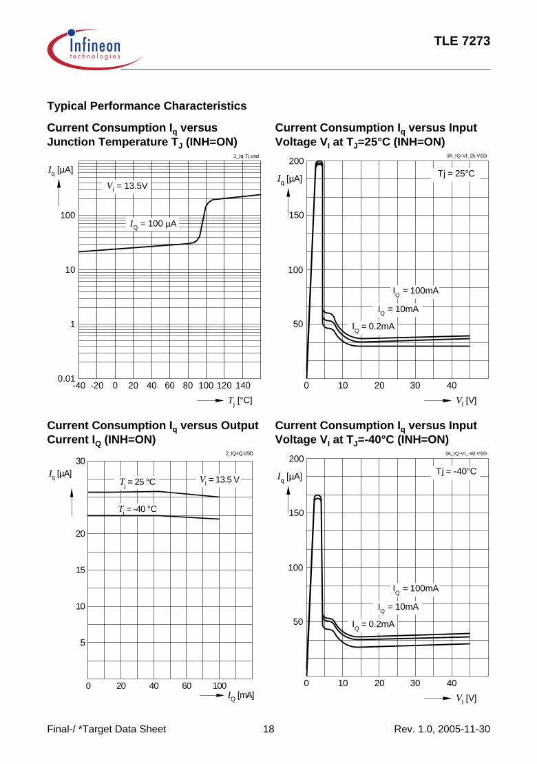
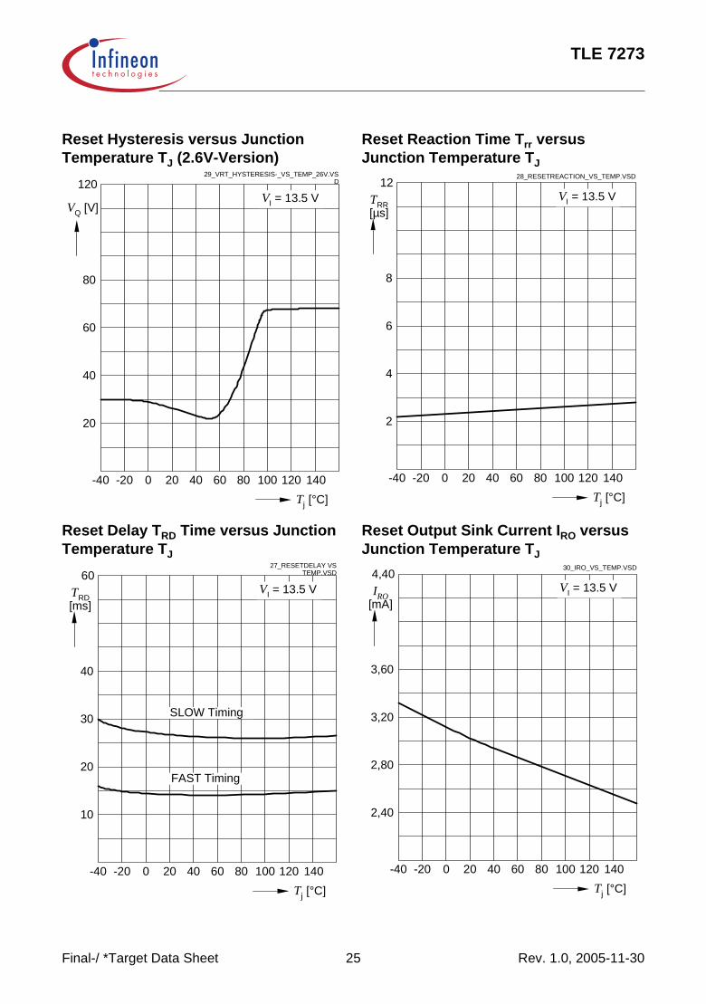
Typical Performance Characteristics
Current Consumption Iq versus Junction Temperature TJ (INH=ON)
Current Consumption Iq versus Output Current IQ (INH=ON)
Current Consumption Iq versus Input Voltage VI at TJ=25°C (INH=ON)
Current Consumption Iq versus Input Voltage VI at TJ=-40°C (INH=ON)
1_Iq-Tj.vsd
10
1
0.01
100
Iq [µA]
-40Tj [°C]
-20 20 40 80 1000 60 140120
VI = 13.5V
IQ = 100 µA
0 40 60
2_IQ-IQ.VSD
15
10
5
20
20 100
Tj = -40 °C
30
Tj = 25 °C
IQ [mA]
Iq [µA] VI = 13.5 V
0VI [V]
20 30
Iq [µA]
3A_IQ-VI_25.VSD
100
50
150
10 40
IQ = 0.2mA
IQ = 10mA
IQ = 100mA
Tj = 25°C200
0VI [V]
20 30
Iq [µA]
3A_IQ-VI_-40.VSD
100
50
150
10 40
IQ = 0.2mA
IQ = 10mA
IQ = 100mA
Tj = -40°C200
Final-/ *Target Data Sheet 19 Rev. 1.0, 2005-11-30
TLE 7273
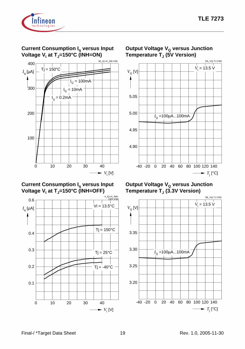
Current Consumption Iq versus Input Voltage VI at TJ=150°C (INH=ON)
Current Consumption Iq versus Input Voltage VI at TJ=150°C (INH=OFF)
Output Voltage VQ versus Junction Temperature TJ (5V Version)
Output Voltage VQ versus Junction Temperature TJ (3.3V Version)
0VI [V]
20 30
Iq [µA]
3A_IQ-VI_150.VSD
200
100
300
10 40
IQ = 0.2mA
IQ = 10mA
IQ = 100mA
Tj = 150°C400
0VI [V]
20 30
Iq [µA]
4_IQ-VI_INH-OFF.VSD
0.3
0.2
0.1
0.4
10 40
Vi = 13.5°C0.6
Tj = 25°C
Tj = 150°C
Tj = -40°C
-40Tj [°C]
-20 20 40 80 100
VQ [V]
5A_VQ-TJ.VSD
5.00
4.95
4.90
5.05
0 60 140120
VI = 13.5 V
IQ =100µA...100mA
-40Tj [°C]
-20 20 40 80 100
VQ [V]
5B_VQ-TJ.VSD
3.30
3.25
3.20
3.35
0 60 140120
VI = 13.5 V
IQ =100µA...100mA
Final-/ *Target Data Sheet 20 Rev. 1.0, 2005-11-30
TLE 7273
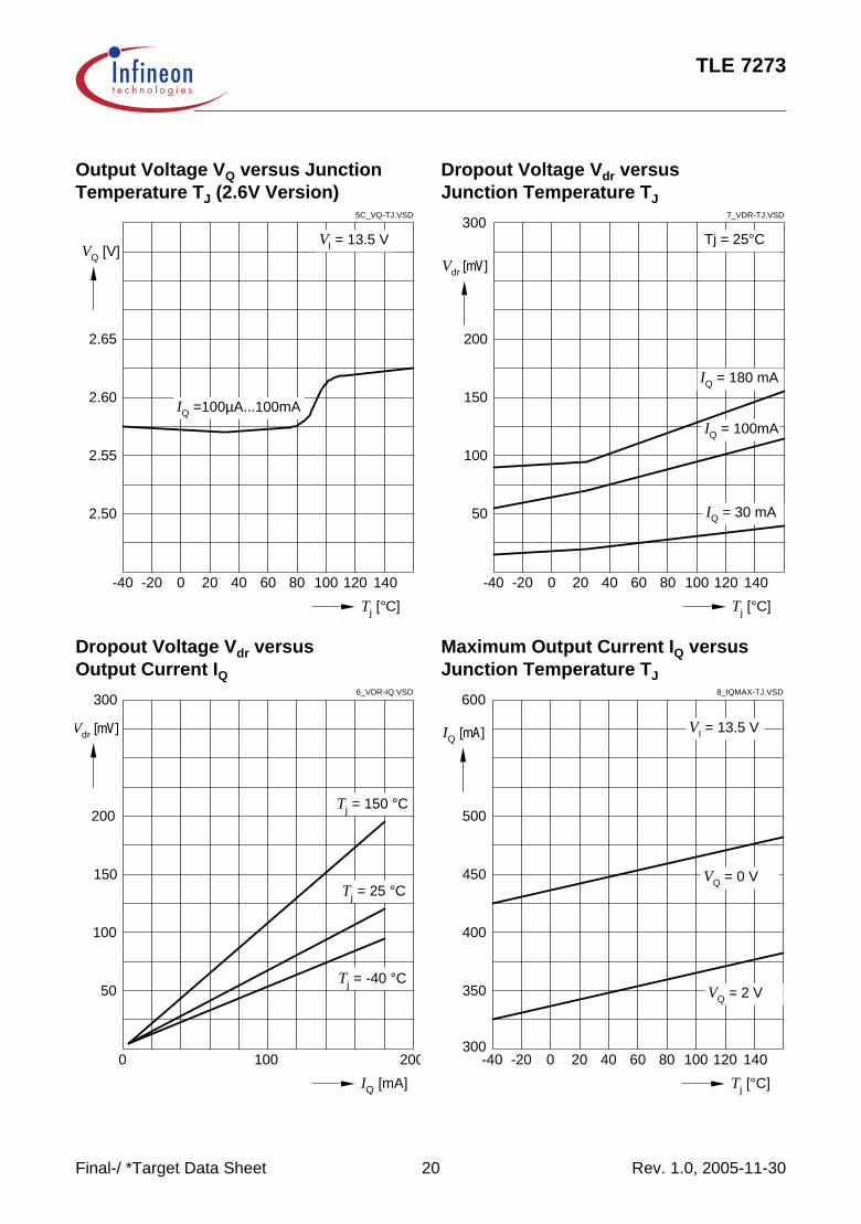
Output Voltage VQ versus Junction Temperature TJ (2.6V Version)
Dropout Voltage Vdr versus Output Current IQ
Dropout Voltage Vdr versus Junction Temperature TJ
Maximum Output Current IQ versus Junction Temperature TJ
-40Tj [°C]
-20 20 40 80 100
VQ [V]
5C_VQ-TJ.VSD
2.60
2.55
2.50
2.65
0 60 140120
VI = 13.5 V
IQ =100µA...100mA
0IQ [mA]
100 200
Vdr [mV]
6_VDR-IQ.VSD
100
200Tj = 150 °C
Tj = 25 °C
Tj = -40 °C
150
50
300
-40Tj [°C]
-20 20 40 80 100
Vdr [mV]
7_VDR-TJ.VSD
150
100
50
200
0 60 140120
IQ = 100mA
300
IQ = 180 mA
IQ = 30 mA
Tj = 25°C
-40Tj [°C]
-20 20 40 80 100
IQ [mA]
8_IQMAX-TJ.VSD
450
400
350
500
0 60 140120
VI = 13.5 V
300
600
VQ = 0 V
VQ = 2 V
Final-/ *Target Data Sheet 21 Rev. 1.0, 2005-11-30
TLE 7273
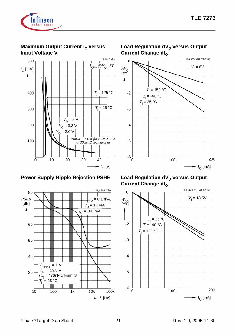
Maximum Output Current IQ versus Input Voltage VI
Power Supply Ripple Rejection PSRR
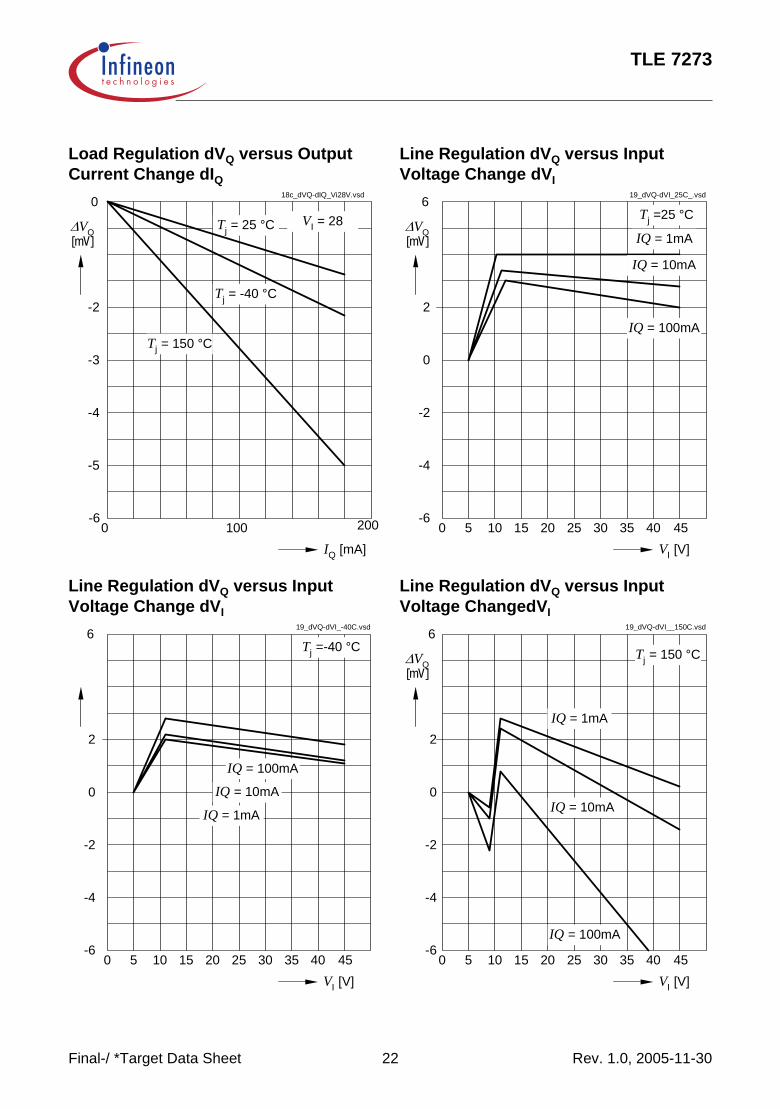
Load Regulation dVQ versus Output Current Change dIQ
Load Regulation dVQ versus Output Current Change dIQ
Attention please!The information given in this data sheet shall in no event be regarded as a guarantee of conditions or characteristics (“Beschaffenheitsgarantie”). With respect to any examples or hints given herein, any typical values stated herein and/or any information regarding the application of the device, Infineon Technologies hereby disclaims any and all warranties and liabilities of any kind, including without limitation warranties of non-infringement of intellectual property rights of any third party.
InformationFor further information on technology, delivery terms and conditions and prices please contact your nearest Infineon Technologies Office (www.infineon.com).
WarningsDue to technical requirements components may contain dangerous substances. For information on the types in question please contact your nearest Infineon Technologies Office.Infineon Technologies Components may only be used in life-support devices or systems with the express written approval of Infineon Technologies, if a failure of such components can reasonably be expected to cause the failure of that life-support device or system, or to affect the safety or effectiveness of that device or system. Life support devices or systems are intended to be implanted in the human body, or to support and/or maintain and sustain and/or protect human life. If they fail, it is reasonable to assume that the health of the user or other persons may be endangered.