Features Load current feedback Programmable over current shutdown Active clamp
ESD protection
Input referenced to Vcc
Over temperature shutdown
Switching time optimized for low EMI
Reverse battery protection
Lead-Free, Halogen-Free, RoHS compliant
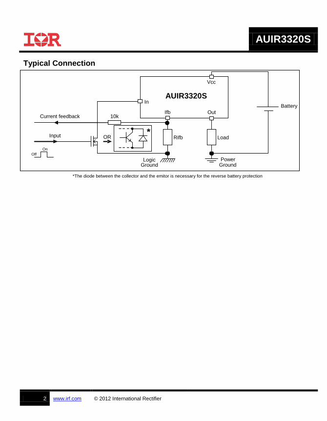
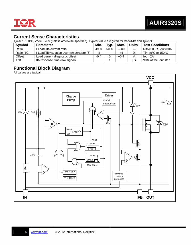
Description The AUIR3320(S) is a fully protected 4 terminals high side switch. The input signal is referenced to Vcc. When the input voltage Vcc - Vin is higher than the specified threshold, the output power Mosfet is turned on. When the Vcc - Vin is lower than the specified Vil threshold, the output Mosfet is turned off. A current proportional to the power Mosfet current is sourced to the Ifb pin. Over current shutdown occurs when Vifb-Vin > 4.7V. The current shutdown threshold is adjusted by selecting the proper RIfb. Either over current and over temperature latches off the switch. The device is reset by pulling the input pin high. Other integrated protections (ESD, reverse battery, active clamp) make the switch very rugged in automotive environment.
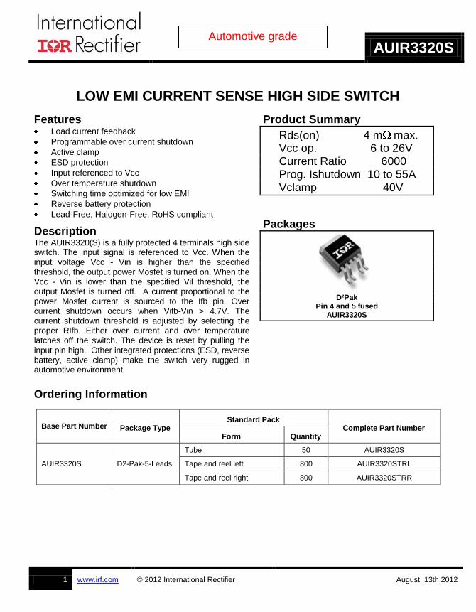
Product Summary
Rds(on) 4 m max. Vcc op. 6 to 26V Current Ratio 6000 Prog. Ishutdown 10 to 55A Vclamp 40V
Absolute Maximum Ratings Absolute maximum ratings indicate sustained limits beyond which damage to the device may occur. All voltage parameters are referenced to Vcc lead. (Tj=-40°..150°C, Vcc=6..26V Tambient=25°C unless otherwise specified).
Symbol Parameter Min. Max. Units Vcc-Vin Maximum Vcc voltage -16 37
V Vcc-Vin cont. Maximum continuous Vcc voltage -16 26
Vcc-Vfb Maximum Ifb voltage -16 33
Vcc-Vout Maximum output voltage -0.3 37
Ids cont. Maximum body diode continuous current Rth=60°C/W (1) Tambient=25°C 2.8 A
Ids pulsed Maximum body diode pulsed current (1) 100
Pd Maximum power dissipation Rth=60°C/W Tambient=25°C 2 W
Tj max. Maximum operating junction temperature -40 150
°C Maximum storage temperature -55 150
Min Rfb Minimum on the resistor on Ifb pin 0.3 k
Ifb max. Max. Ifb current -50 50 mA
(1) Limited by junction temperature. Pulsed is also limited by wiring
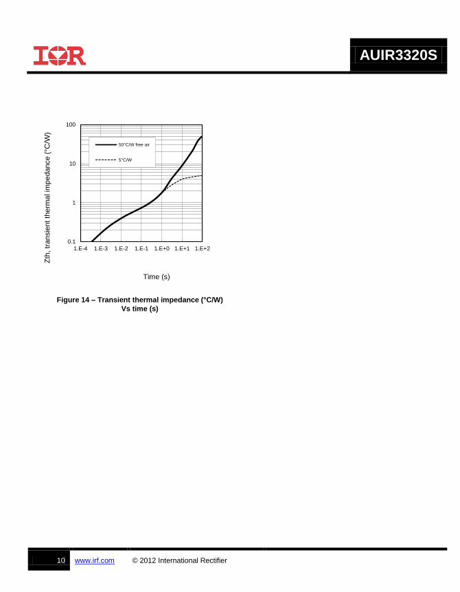
Thermal Characteristics Symbol Parameter Typ. Max. Units Rth1 Thermal resistance junction to ambient D²-Pak Std footprint 60
Rth3 Thermal resistance junction to case D²-Pak 0.7
Recommended Operating Conditions These values are given for a quick design. For operation outside these conditions, please consult the application notes.
Symbol Parameter Min. Max. Units
Iout
Continuous output current
A Tambient=85°C, Rth=5°C/W, Tj=150°C 45
Tambient=85°C, Rth=40°C/W, Tj=150°C 16
Rifb Recommended Ifb resistor (2)(3) 0.3 3.5 k
Pulse min. Minimum turn-on pulse width 1 ms
Fmax. Maximum operating frequency 200 Hz
(2) If Rifb is too low, the device can be damaged. (3) If Rifb is too high, the device may not switch on.
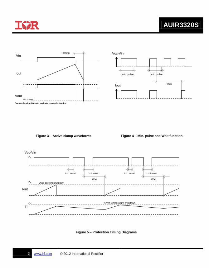
Protection Characteristics Tj=-40°..150°C, Vcc=6..26V, Rifb=500 to 3.5k . Typical value are given for Vcc=14V and Tj=25°C
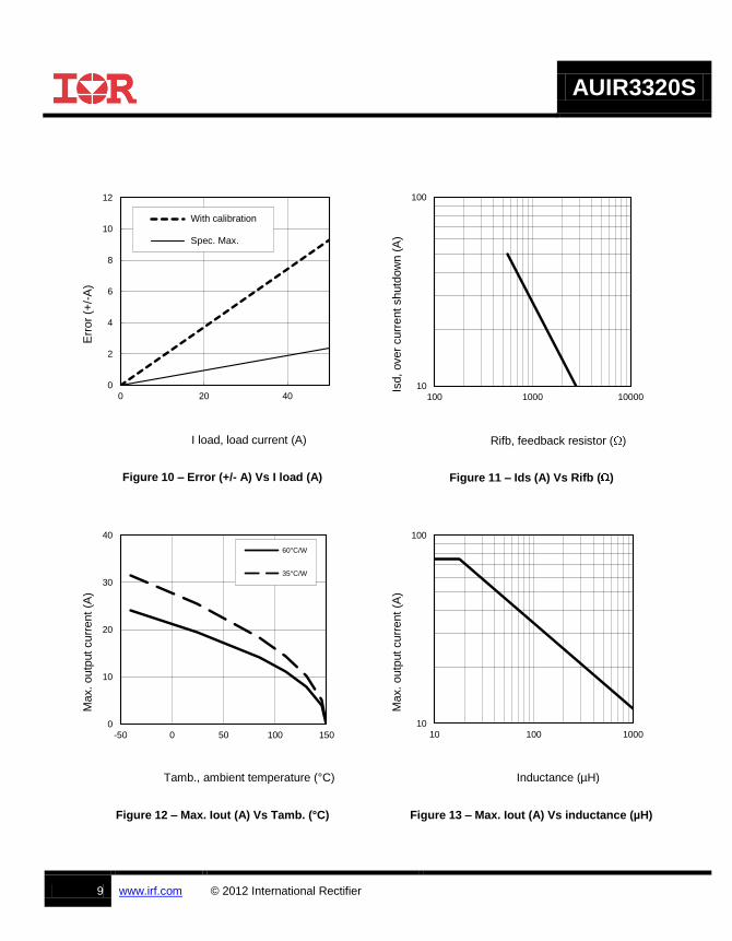
Symbol Parameter Min. Typ. Max. Units Test Conditions Vifb-Vin@Isd Over-current shutdown threshold 3.8 4.7 5.9 V
Tsd Over temperature threshold 165 °C See fig. 5
OV Over voltage protection (not latched) 26 29 33 V
Isdf Fixed over current shutdown 55 75 105 A
Vifb<Vifb-Vin@Isd
Isd_560 Programmable over current shutdown 34 50 71 Rifb=560
Treset Time to reset protection 50 500 µs
See fig. 5
Min. pulse Min. pulse width (no WAIT state) 900 2000 Tj=25°C
WAIT WAIT function timer 0.4 1 2 ms See fig. 4 and 5
Rds(on) rev. Reverse battery On state resistance, Tj=25°C
4 6 m
Vcc-Vin=-14V, Iout=30A
Tj=125°C 6 9
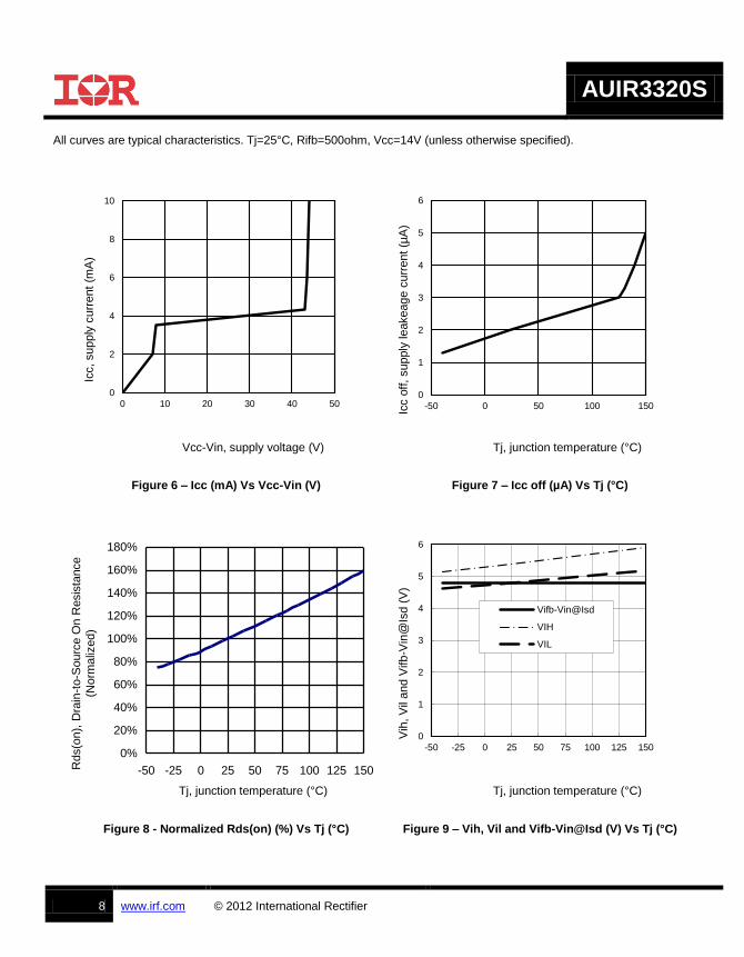
Static Electrical Characteristics Tj=-40°..150°C, Vcc=6..26V (unless otherwise specified). Typical value are given for Vcc=14V and Tj=25°C
Symbol Parameter Min. Typ. Max. Units Test Conditions Vcc op. Operating Voltage range 6 26 V
Icc off Supply leakage current 1.5 5 µA Vin=Vcc, Vcc-Vout=14V, Vcc-Vifb=14V, Tj=25°C
Iin, on On state IN positive current 1.5 3 6 mA Vcc-Vin=14V, Tj=25°C
Vih High level Input threshold voltage (4) 5.4 6.3
V
Vil Low level Input threshold voltage (4) 4 4.9 5.8
Vhyst Input hysteresis Vih-Vil 0.2 0.4 1.5
Iout Drain to source leakage current 1.2 5 µA Vin=Vcc, Vcc-Vifb=0V, Vcc-Vout=14V, Tj=25°C
Rds(on)
On state resistance (5) Tj=25°C 3.3 4
m
Iout=30A, Vcc-Vin=14V
On state resistance (5) Tj=25°C 3.5 5.5 Iout=17A, Vcc-Vin=6V
On state resistance (5)(6) Tj=150°C 5.5 6.5 Iout=30A, Vcc-Vin=14V
V clamp1 Vcc to Vout clamp voltage 1 36 39 43 V
Iout=50mA
V clamp2 Vcc to Vout clamp voltage 2 40 Iout=30A, Tj=25°C
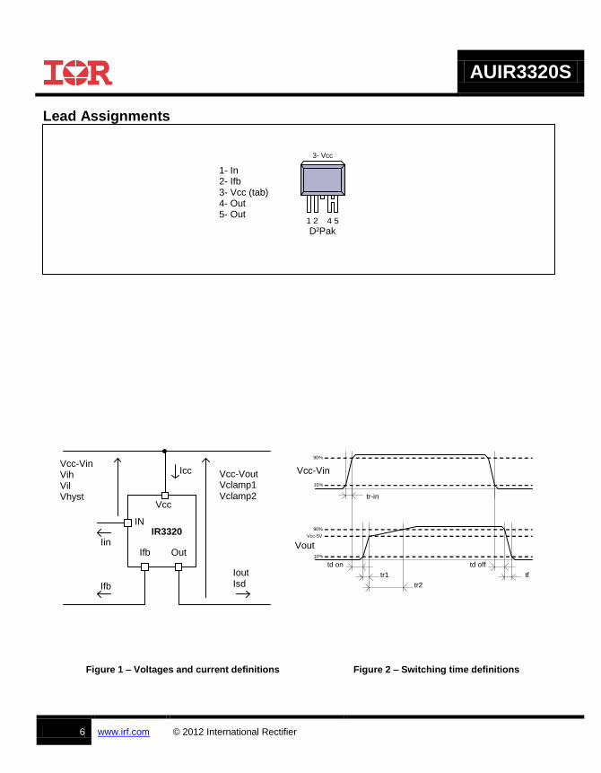
(4) Input thresholds are measured directly between the input pin and the tab. Any parasitic resistance in common between the load current path and the input signal path can significantly affect the thresholds. (5) Rdson is measured between the tab and the Out pin, 5mm away from the package. (6) Guaranteed by design
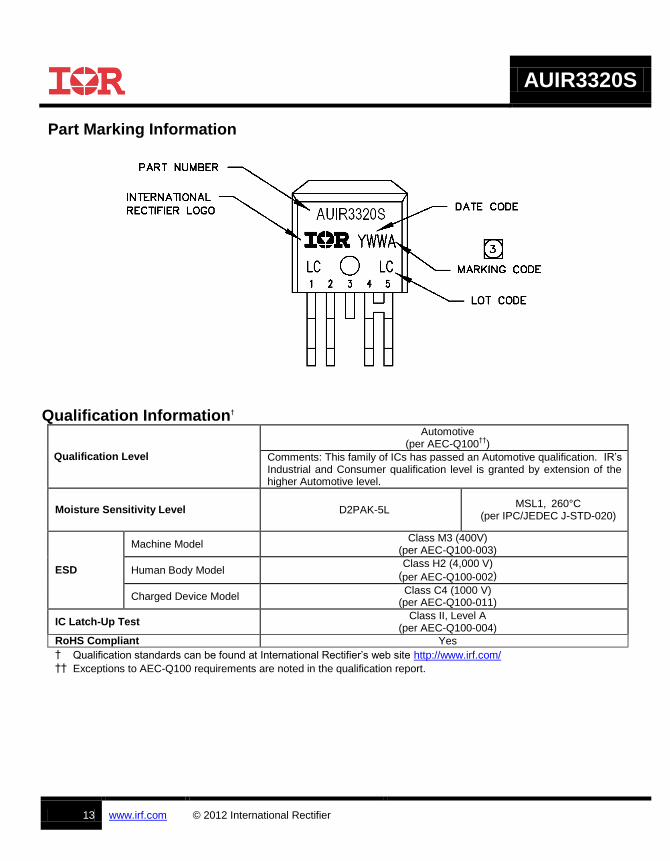
Comments: This family of ICs has passed an Automotive qualification. IR’s Industrial and Consumer qualification level is granted by extension of the higher Automotive level.
Moisture Sensitivity Level D2PAK-5L MSL1,
260°C
(per IPC/JEDEC J-STD-020)
ESD
Machine Model Class M3 (400V)
(per AEC-Q100-003)
Human Body Model Class H2 (4,000 V)
(per AEC-Q100-002)
Charged Device Model Class C4 (1000 V)
(per AEC-Q100-011)
IC Latch-Up Test Class II, Level A
(per AEC-Q100-004)
RoHS Compliant Yes
† Qualification standards can be found at International Rectifier’s web site http://www.irf.com/
†† Exceptions to AEC-Q100 requirements are noted in the qualification report.
IMPORTANT NOTICE Unless specifically designated for the automotive market, International Rectifier Corporation and its subsidiaries (IR) reserve the right to make corrections, modifications, enhancements, improvements, and other changes to its products and services at any time and to discontinue any product or services without notice. Part numbers designated with the “AU” prefix follow automotive industry and / or customer specific requirements with regards to product discontinuance and process change notification. All products are sold subject to IR’s terms and conditions of sale supplied at the time of order acknowledgment. IR warrants performance of its hardware products to the specifications applicable at the time of sale in accordance with IR’s standard warranty. Testing and other quality control techniques are used to the extent IR deems necessary to support this warranty. Except where mandated by government requirements, testing of all parameters of each product is not necessarily performed. IR assumes no liability for applications assistance or customer product design. Customers are responsible for their products and applications using IR components. To minimize the risks with customer products and applications, customers should provide adequate design and operating safeguards. Reproduction of IR information in IR data books or data sheets is permissible only if reproduction is without alteration and is accompanied by all associated warranties, conditions, limitations, and notices. Reproduction of this information with alterations is an unfair and deceptive business practice. IR is not responsible or liable for such altered documentation. Information of third parties may be subject to additional restrictions. Resale of IR products or serviced with statements different from or beyond the parameters stated by IR for that product or service voids all express and any implied warranties for the associated IR product or service and is an unfair and deceptive business practice. IR is not responsible or liable for any such statements. IR products are not designed, intended, or authorized for use as components in systems intended for surgical implant into the body, or in other applications intended to support or sustain life, or in any other application in which the failure of the IR product could create a situation where personal injury or death may occur. Should Buyer purchase or use IR products for any such unintended or unauthorized application, Buyer shall indemnify and hold International Rectifier and its officers, employees, subsidiaries, affiliates, and distributors harmless against all claims, costs, damages, and expenses, and reasonable attorney fees arising out of, directly or indirectly, any claim of personal injury or death associated with such unintended or unauthorized use, even if such claim alleges that IR was negligent regarding the design or manufacture of the product. IR products are neither designed nor intended for use in military/aerospace applications or environments unless the IR products are specifically designated by IR as military-grade or “enhanced plastic.” Only products designated by IR as military-grade meet military specifications. Buyers acknowledge and agree that any such use of IR products which IR has not designated as military-grade is solely at the Buyer’s risk, and that they are solely responsible for compliance with all legal and regulatory requirements in connection with such use. IR products are neither designed nor intended for use in automotive applications or environments unless the specific IR products are designated by IR as compliant with ISO/TS 16949 requirements and bear a part number including the designation “AU”. Buyers acknowledge and agree that, if they use any non-designated products in automotive applications, IR will not be responsible for any failure to meet such requirements.
For technical support, please contact IR’s Technical Assistance Center
http://www.irf.com/technical-info/ WORLD HEADQUARTERS:
101 N Sepulveda Blvd., El Segundo, California 90245 Tel: (310) 252-7105