Low-Noise, Fixed Drop-Out, ±2.5- to ±12-VOUT, 3-A Power Supply ReferenceDesign for Ultrasound CW Pulser
TI Designs: TIDA-01458Low-Noise, Fixed Drop-Out, ±2.5- to ±12-VOUT, 3-A PowerSupply Reference Design for Ultrasound CW Pulser
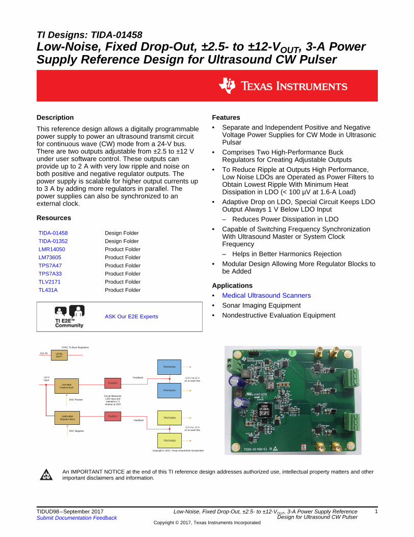
DescriptionThis reference design allows a digitally programmablepower supply to power an ultrasound transmit circuitfor continuous wave (CW) mode from a 24-V bus.There are two outputs adjustable from ±2.5 to ±12 Vunder user software control. These outputs canprovide up to 2 A with very low ripple and noise onboth positive and negative regulator outputs. Thepower supply is scalable for higher output currents upto 3 A by adding more regulators in parallel. Thepower supplies can also be synchronized to anexternal clock.
Features• Separate and Independent Positive and Negative
Voltage Power Supplies for CW Mode in UltrasonicPulsar
• Comprises Two High-Performance BuckRegulators for Creating Adjustable Outputs
• To Reduce Ripple at Outputs High Performance,Low Noise LDOs are Operated as Power Filters toObtain Lowest Ripple With Minimum HeatDissipation in LDO (< 100 µV at 1.6-A Load)
• Adaptive Drop on LDO, Special Circuit Keeps LDOOutput Always 1 V Below LDO Input– Reduces Power Dissipation in LDO
• Capable of Switching Frequency SynchronizationWith Ultrasound Master or System ClockFrequency– Helps in Better Harmonics Rejection
• Modular Design Allowing More Regulator Blocks tobe Added
Applications• Medical Ultrasound Scanners• Sonar Imaging Equipment• Nondestructive Evaluation Equipment
An IMPORTANT NOTICE at the end of this TI reference design addresses authorized use, intellectual property matters and otherimportant disclaimers and information.
Low-Noise, Fixed Drop-Out, ±2.5- to ±12-VOUT, 3-A Power Supply ReferenceDesign for Ultrasound CW Pulser
1 System DescriptionThis design guide describes a power supply for continuous wave (CW) mode. These typically need ±2.5 to±12 V under software control. Budget a current delivery up to 3 A at outputs of DC-DC converters. Inaddition, the power supplies must have a very low level of ripple and noise at the output voltage.
1.1 Basic Ultrasound SystemIn an ultrasound system, the transmitter that generates high-voltage signals to excite a transducer is oneof the most critical components in the entire ultrasonic diagnostic system. There are semiconductordevices available that can generate high-voltage signals to ensure the penetration depth of ultrasonicsignals. A generic system-level block diagram for a cart-based ultrasound scanner is shown in Figure 1.
Figure 1. System-Level Block Diagram for Cart-Based Ultrasound Scanners
The high-voltage pulses (to be transmitted inside human body to get information about blood, organs,tissues, and so on) are bipolar in nature and are transmitted by transmitters (TXs). There are two modesin general:1. Pulse (also known as brightness, or B) mode where high-voltage pulses (–100 V and 100 V, typically)
are transmitted for a particular short time only.2. CW mode where low-voltage (±2.5 to ±10 V, typically) pulses are continuously transmitted.
Low-Noise, Fixed Drop-Out, ±2.5- to ±12-VOUT, 3-A Power Supply ReferenceDesign for Ultrasound CW Pulser
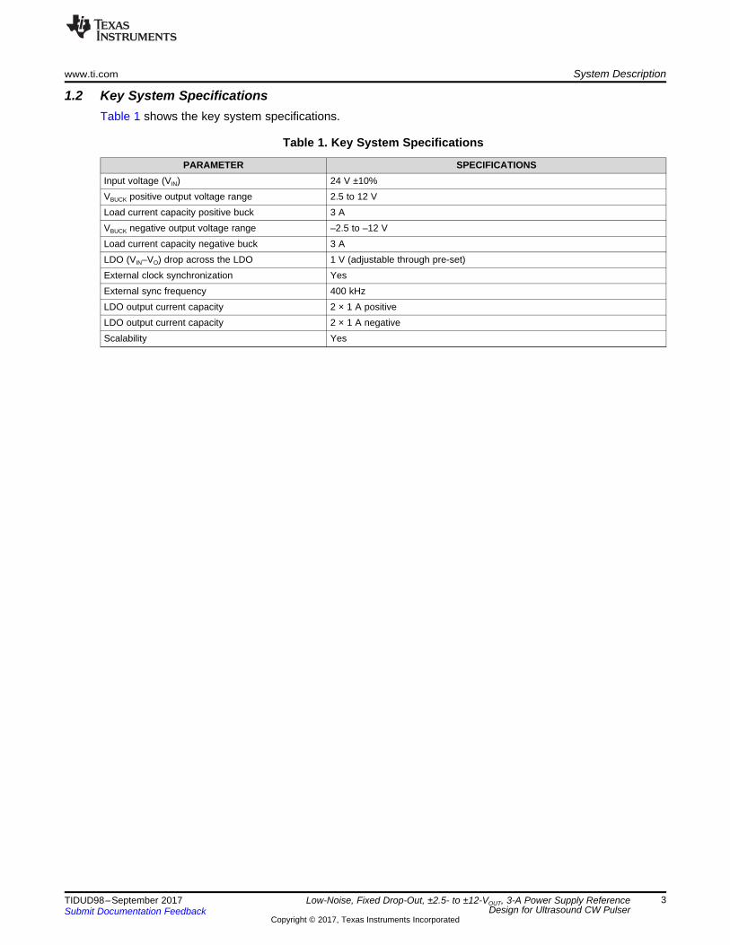
1.2 Key System SpecificationsTable 1 shows the key system specifications.
Table 1. Key System Specifications
PARAMETER SPECIFICATIONSInput voltage (VIN) 24 V ±10%VBUCK positive output voltage range 2.5 to 12 VLoad current capacity positive buck 3 AVBUCK negative output voltage range –2.5 to –12 VLoad current capacity negative buck 3 ALDO (VIN–VO) drop across the LDO 1 V (adjustable through pre-set)External clock synchronization YesExternal sync frequency 400 kHzLDO output current capacity 2 × 1 A positiveLDO output current capacity 2 × 1 A negativeScalability Yes
Low-Noise, Fixed Drop-Out, ±2.5- to ±12-VOUT, 3-A Power Supply ReferenceDesign for Ultrasound CW Pulser
2 System Overview
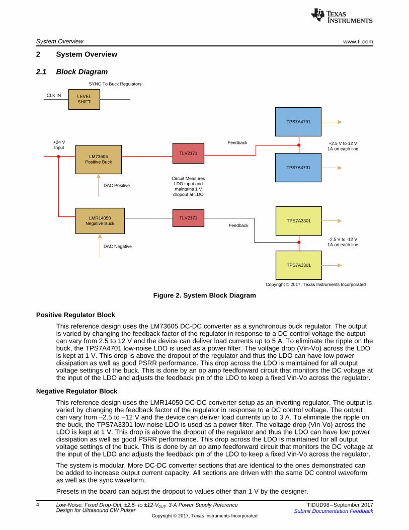
2.1 Block Diagram
Figure 2. System Block Diagram
Positive Regulator BlockThis reference design uses the LM73605 DC-DC converter as a synchronous buck regulator. The outputis varied by changing the feedback factor of the regulator in response to a DC control voltage the outputcan vary from 2.5 to 12 V and the device can deliver load currents up to 5 A. To eliminate the ripple on thebuck, the TPS7A4701 low-noise LDO is used as a power filter. The voltage drop (Vin-Vo) across the LDOis kept at 1 V. This drop is above the dropout of the regulator and thus the LDO can have low powerdissipation as well as good PSRR performance. This drop across the LDO is maintained for all outputvoltage settings of the buck. This is done by an op amp feedforward circuit that monitors the DC voltage atthe input of the LDO and adjusts the feedback pin of the LDO to keep a fixed Vin-Vo across the regulator.
Negative Regulator BlockThis reference design uses the LMR14050 DC-DC converter setup as an inverting regulator. The output isvaried by changing the feedback factor of the regulator in response to a DC control voltage. The outputcan vary from –2.5 to –12 V and the device can deliver load currents up to 3 A. To eliminate the ripple onthe buck, the TPS7A3301 low-noise LDO is used as a power filter. The voltage drop (Vin-Vo) across theLDO is kept at 1 V. This drop is above the dropout of the regulator and thus the LDO can have low powerdissipation as well as good PSRR performance. This drop across the LDO is maintained for all outputvoltage settings of the buck. This is done by an op amp feedforward circuit that monitors the DC voltage atthe input of the LDO and adjusts the feedback pin of the LDO to keep a fixed Vin-Vo across the regulator.
The system is modular. More DC-DC converter sections that are identical to the ones demonstrated canbe added to increase output current capacity. All sections are driven with the same DC control waveformas well as the sync waveform.
Presets in the board can adjust the dropout to values other than 1 V by the designer.
Low-Noise, Fixed Drop-Out, ±2.5- to ±12-VOUT, 3-A Power Supply ReferenceDesign for Ultrasound CW Pulser
2.2 Highlighted Products
2.2.1 LM73605The LM73605 device is a synchronous step-down DC-DC converter capable of driving 5 A from a supplyvoltage from 3.5- to 36-V DC. It has high efficiency and a high-output accuracy in a small solution size.Peak current mode control is employed. The device has an adjustable frequency and also allowsfrequency synchronization.
2.2.2 LMR14050The LMR14050 device is an integrated 40-V, 5-A step-down regulator with an integrated switching FET.The device has an ultra-low quiescent current of 1 µA in sleep mode. It has an adjustable switchingfrequency range and internal loop compensation .It also has cycle-by-cycle current limit, thermal sensing,and shutdown.
2.2.3 TPS7A4701The TPS7A4701 device is a positive voltage (36 V), ultra-low-noise (4 µVRMS) low-dropout linear regulator(LDO) capable of sourcing a 1-A load.
2.2.4 TPS7A3301The TPS7A3301 device is a negative voltage (–36 V), ultra-low-noise (16-μVRMS, 72-dB PSRR) linearregulator capable of sourcing a maximum load of 1 A.
2.2.5 TLV2171The 36-V TLV2171 device provides a low-power option for cost-conscious industrial and personalelectronics systems requiring an electromagnetic interference (EMI)-hardened, low-noise, single-supplyoperational amplifier (op amp) that operates on supplies ranging from 2.7 V (±1.35 V) to 36 V (±18 V).
Low-Noise, Fixed Drop-Out, ±2.5- to ±12-VOUT, 3-A Power Supply ReferenceDesign for Ultrasound CW Pulser
2.3.1 Positive Switching RegulatorsThe LM73605 (U1) is a synchronous buck regulator that can drive 5 A of current. The output voltage istypically set up by R7 and R4. The feedback pin is normally regulated to 1 V. A DC control voltagebetween 0 and 3.3 V applied to Pin 1 of J1 is used to modify the output of the buck regulator from 2.5 to15 V. This voltage is applied to U2B. This is an op amp buffer and its output is connected to a low-passfilter comprising of R8 and C17. The low-pass filter ensures that a pure DC voltage is applied to thefeedback pin. Assume that the control voltage on Pin 1 of JI is 0 V. The output of op amp U2B is also 0 V.
(1)
Assume now that 3-V DC is applied on Pin 1 of J1. The output of the op amp is now 1-V DC. Applying thesuperposition theorem on the feedback pin:
(2)
Therefore, for a DAC control range of 0 3 V, the output voltage varies from 1 to 15.7 V.(3)
This is an approximate equation describing the behavior given the resistors placed R58 on pin 9 of U1sets the operating frequency of the DC-DC converter.
Low-Noise, Fixed Drop-Out, ±2.5- to ±12-VOUT, 3-A Power Supply ReferenceDesign for Ultrasound CW Pulser
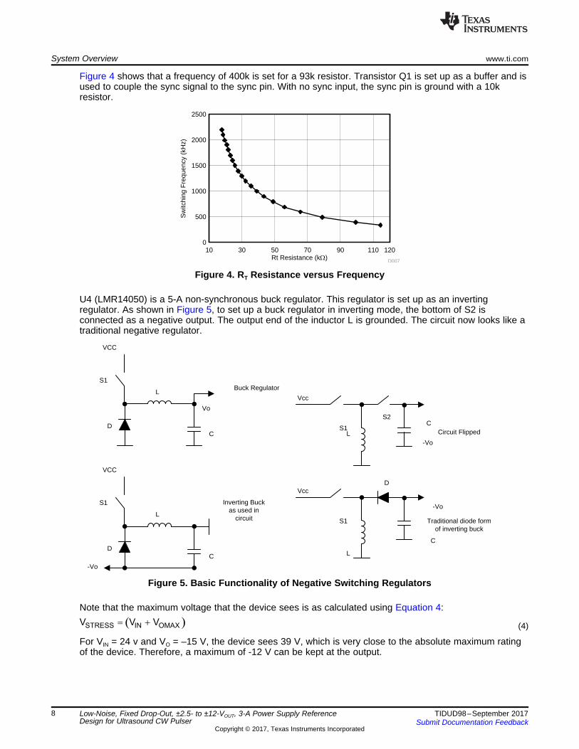
Figure 4 shows that a frequency of 400k is set for a 93k resistor. Transistor Q1 is set up as a buffer and isused to couple the sync signal to the sync pin. With no sync input, the sync pin is ground with a 10kresistor.
Figure 4. RT Resistance versus Frequency
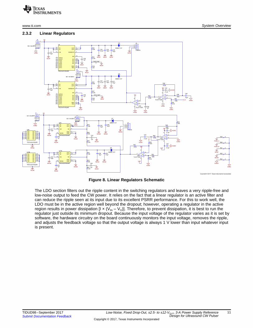
U4 (LMR14050) is a 5-A non-synchronous buck regulator. This regulator is set up as an invertingregulator. As shown in Figure 5, to set up a buck regulator in inverting mode, the bottom of S2 isconnected as a negative output. The output end of the inductor L is grounded. The circuit now looks like atraditional negative regulator.
Figure 5. Basic Functionality of Negative Switching Regulators
Note that the maximum voltage that the device sees is as calculated using Equation 4:
(4)
For VIN = 24 v and VO = –15 V, the device sees 39 V, which is very close to the absolute maximum ratingof the device. Therefore, a maximum of -12 V can be kept at the output.
Low-Noise, Fixed Drop-Out, ±2.5- to ±12-VOUT, 3-A Power Supply ReferenceDesign for Ultrasound CW Pulser
Figure 6. Theoretical Waveforms for Negative Buck
Regarding Figure 6, assume TON is the time S1 conducts and TOFF is the time S2 conducts.
(5)
Note that IO = Average of IS2.
(6)
Therefore, if VO = –15 V, D = 0.36, IO maximum = 3 A for a 5-A buck switcher. Resistors R27 and R56 areused to set the output voltage. The LMR14050 has a feedback voltage of 0.75 V.
(7)
To adjust the negative output, apply a DC control voltage between 0 and 3 V to Pin 2 of J1.
Low-Noise, Fixed Drop-Out, ±2.5- to ±12-VOUT, 3-A Power Supply ReferenceDesign for Ultrasound CW Pulser
The collector of Q5 adds a voltage to the feedback pin of the LMR14050. When this voltage from thefeedback pin to the device ground equals 0.75 V, the output of the negative converter drops to zero. The0.75 V is obtained through the op amp current source. When the DC voltage applied to pin 3, U2A is 0 V.The current in Q5 = 3.3/R16 or 3.3/3K3 = 1 mA. R66 × 1 mA = 1 V. This is more than the 0.75 V neededto bring the output voltage to zero.
This is an approximate equation describing the behavior given the resistors placed R25 is used to set theoscillator frequency at 400k.
Transistor Q4 is used to couple the sync signals to the RT pin. When there is no sync signal, the transistoris cut off. The Enable pin is driven by transistor Q6. This transistor acts as a level shifter as the Enable pinis referenced to –VO. Resistors R22 and R23 act as a voltage divider and at a minimum supply voltageturn the PNP transistor on
Low-Noise, Fixed Drop-Out, ±2.5- to ±12-VOUT, 3-A Power Supply ReferenceDesign for Ultrasound CW Pulser
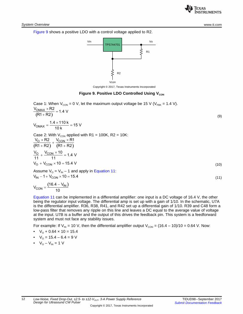
2.3.2 Linear Regulators
Figure 8. Linear Regulators Schematic
The LDO section filters out the ripple content in the switching regulators and leaves a very ripple-free andlow-noise output to feed the CW power. It relies on the fact that a linear regulator is an active filter andcan reduce the ripple seen at its input due to its excellent PSRR performance. For this to work well, theLDO must be in the active region well beyond the dropout; however, operating a regulator in the activeregion results in power dissipation [I × (VIN – VO)]. Therefore, to prevent dissipation, it is best to run theregulator just outside its minimum dropout. Because the input voltage of the regulator varies as it is set bysoftware, the hardware circuitry on the board continuously monitors the input voltage, removes the ripple,and adjusts the feedback voltage so that the output voltage is always 1 V lower than input whatever inputis present.
Low-Noise, Fixed Drop-Out, ±2.5- to ±12-VOUT, 3-A Power Supply ReferenceDesign for Ultrasound CW Pulser
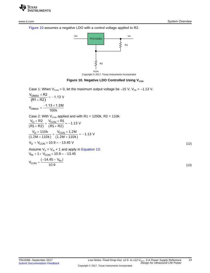
Figure 9 shows a positive LDO with a control voltage applied to R2.
Figure 9. Positive LDO Controlled Using VCON
Case 1: When VCON = 0 V, let the maximum output voltage be 15 V (VFBK = 1.4 V).
(9)
Case 2: With VCON applied with R1 = 100K, R2 = 10K:
(10)
Assume VO = VIN – 1 and apply in Equation 11:(11)
Equation 11 can be implemented in a differential amplifier: one input is a DC voltage of 16.4 V, the otherbeing the regulator input voltage. The differential amp is set up with a gain of 1/10. In the schematic, U7Ais the differential amplifier. R36, R38, R41, and R42 set up a differential gain of 1/10. R39 and C48 form alow-pass filter that removes any ripple on this line and leaves a DC equal to the average value of voltageat the input. U7B is a buffer and the output of this drives the feedback pin. This system is a feedforwardsystem and must not face any stability issues.
For example: If VIN = 10 V, then the differential amplifier output VCON = (16.4 – 10)/10 = 0.64 V. Now:• VO + 0.64 × 10 = 15.4• VO = 15.4 – 6.4 = 9 V• VO – VIN = 1 V
Low-Noise, Fixed Drop-Out, ±2.5- to ±12-VOUT, 3-A Power Supply ReferenceDesign for Ultrasound CW Pulser
Equation 13 can be implemented in a differential amplifier: one input is a DC voltage of 15.7 V, the otherbeing the regulator input voltage. U9A is a differential amplifier with a gain of –1. This converts thenegative input voltage to a positive output level. U9B is a differential amplifier with a gain 1/10.9 thatcompares the positive output voltage seen on U9A with a fixed DC voltage of –14.45 V. For example: Ifthe VIN of the regulator is –10 V, pin 1 of U9A would be 10 V as U9A is an inverting amplifier with a gain of1. The output of U9B that is a differential amplifier with an attenuation of 1/12 would be as follows:• From Equation 13:
• From Equation 12:
This is VIN + 1. The drop across the LDO is 1 V. Therefore, the drop across the differential amplifier needsto be –0.4 V. The differential amplifier implements
(14)
R47 and C53 form a low-pass filter that removes any ripple present on the input of the LDO. ORing diodesD5, D6, D7, and D8 are used to connect the output with the high-voltage supply. The diodes would blockthe high voltages from reaching the regulators. The control loop is common to all the LDOs, and it ispossible to place many LDOs on the same control loop to share the currents.
Low-Noise, Fixed Drop-Out, ±2.5- to ±12-VOUT, 3-A Power Supply ReferenceDesign for Ultrasound CW Pulser
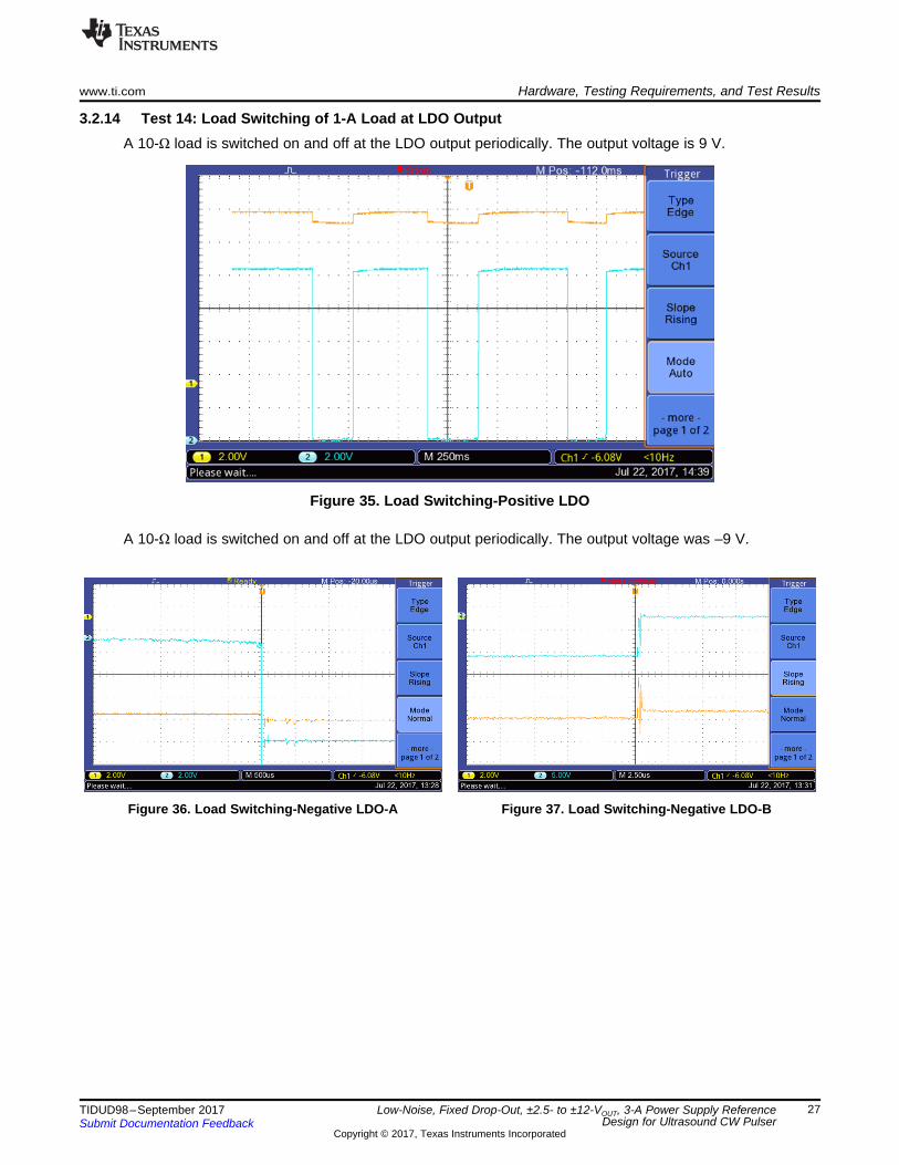
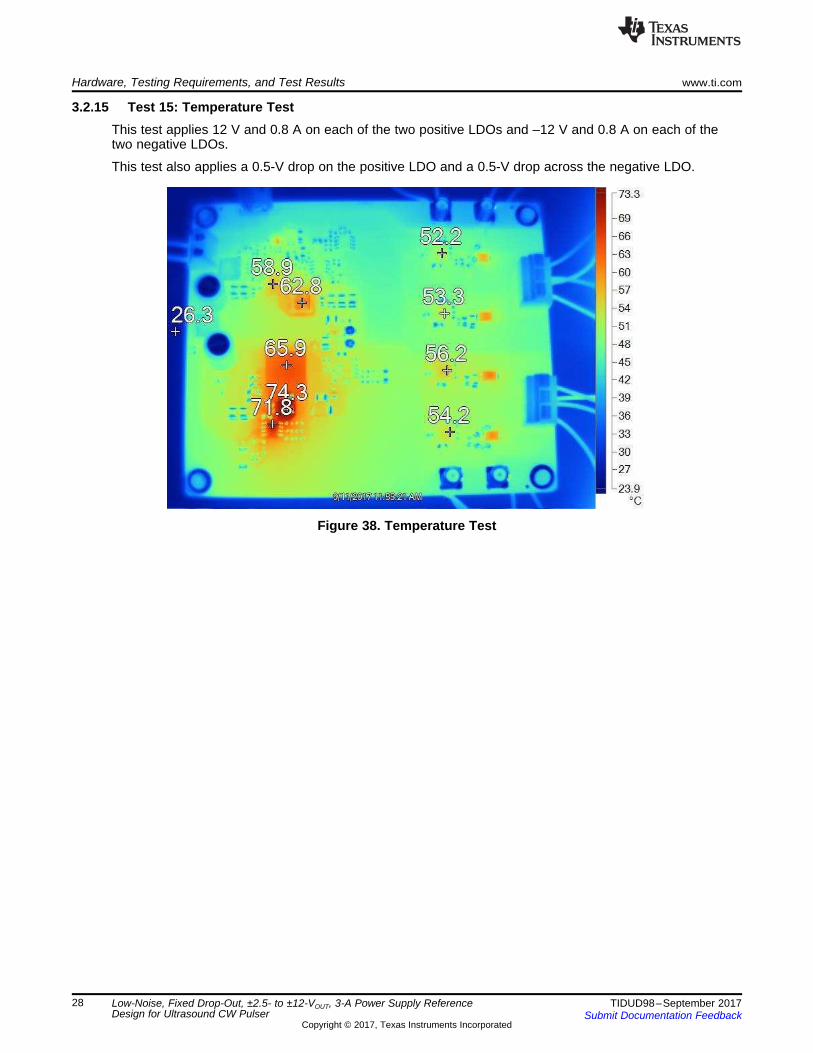
3.2 Testing and ResultsTo test the board, use the following equipment:• 24-V DC input supply rated at 5 A• 5-V variable DC source to provide a control signal to adjust the output voltages• 15-Ω power resistors as well as an electronic load is also needed• 5-V pulses frequency source capable of generating frequencies from 300 to 500 kHz• Oscilloscope (100 MHz)• Spectrum analyzer• Thermal camera
3.2.1 Test 1: Output Voltages as a Function of Control Voltage-Negative Power SupplyA load of 0.8 A is put on the output of the LDO, and the output voltage is observed as a function of DCcontrol voltage.
Figure 13. Output Voltage as Function of DC Control-Negative
3.2.2 Test 2: Voltage Drop Across Negative LDO as a Function of Control VoltageA load of 0.8 A is put on the output of the LDO, and the voltage drop across the LDO is observed forvarying DC-DC converter outputs.
Low-Noise, Fixed Drop-Out, ±2.5- to ±12-VOUT, 3-A Power Supply ReferenceDesign for Ultrasound CW Pulser
3.2.3 Test 3: Output Voltages as a Function of Control Voltage-Positive Power SupplyA load of 0.8 A is put on the output of the LDO, and the output voltage is observed as a function of DCcontrol voltage.
Figure 15. Output Voltage as Function of DC Control-Positive
3.2.4 Test 4: Voltage Drop Across Positive LDO as a Function of Control VoltageA load of 0.8 A is put on the output of the LDO, and the voltage drop across the LDO is observed forvarying DC-DC converter outputs.
Low-Noise, Fixed Drop-Out, ±2.5- to ±12-VOUT, 3-A Power Supply ReferenceDesign for Ultrasound CW Pulser
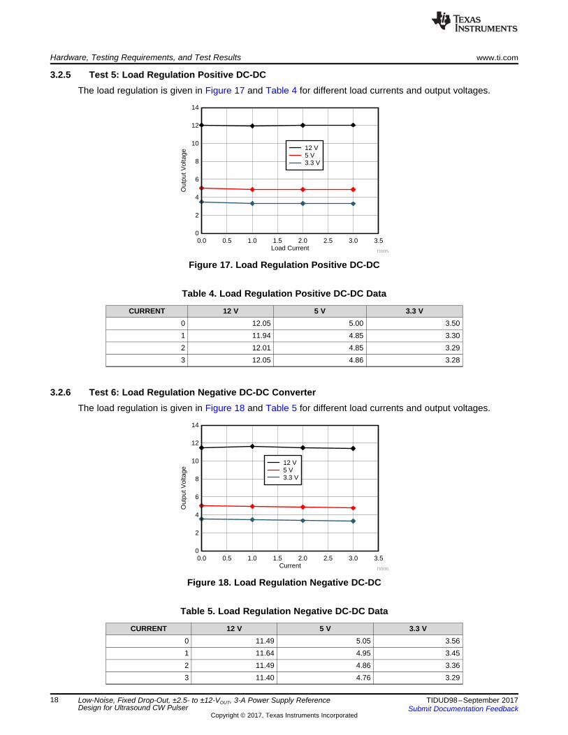
3.2.5 Test 5: Load Regulation Positive DC-DCThe load regulation is given in Figure 17 and Table 4 for different load currents and output voltages.
Figure 17. Load Regulation Positive DC-DC
Table 4. Load Regulation Positive DC-DC Data
CURRENT 12 V 5 V 3.3 V0 12.05 5.00 3.501 11.94 4.85 3.302 12.01 4.85 3.293 12.05 4.86 3.28
3.2.6 Test 6: Load Regulation Negative DC-DC ConverterThe load regulation is given in Figure 18 and Table 5 for different load currents and output voltages.
Figure 18. Load Regulation Negative DC-DC
Table 5. Load Regulation Negative DC-DC Data
CURRENT 12 V 5 V 3.3 V0 11.49 5.05 3.561 11.64 4.95 3.452 11.49 4.86 3.363 11.40 4.76 3.29
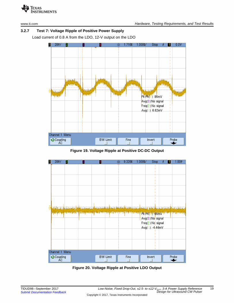
Low-Noise, Fixed Drop-Out, ±2.5- to ±12-VOUT, 3-A Power Supply ReferenceDesign for Ultrasound CW Pulser
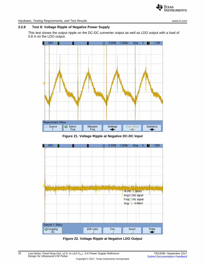
3.2.8 Test 8: Voltage Ripple of Negative Power SupplyThis test shows the output ripple on the DC-DC converter output as well as LDO output with a load of0.8 A on the LDO output.
Low-Noise, Fixed Drop-Out, ±2.5- to ±12-VOUT, 3-A Power Supply ReferenceDesign for Ultrasound CW Pulser
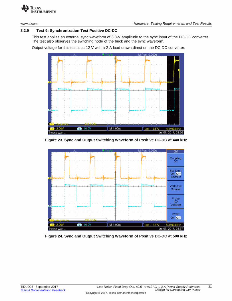
3.2.9 Test 9: Synchronization Test Positive DC-DCThis test applies an external sync waveform of 3.3-V amplitude to the sync input of the DC-DC converter.The test also observes the switching node of the buck and the sync waveform.
Output voltage for this test is at 12 V with a 2-A load drawn direct on the DC-DC converter.
Figure 23. Sync and Output Switching Waveform of Positive DC-DC at 440 kHz
Figure 24. Sync and Output Switching Waveform of Positive DC-DC at 500 kHz
Low-Noise, Fixed Drop-Out, ±2.5- to ±12-VOUT, 3-A Power Supply ReferenceDesign for Ultrasound CW Pulser
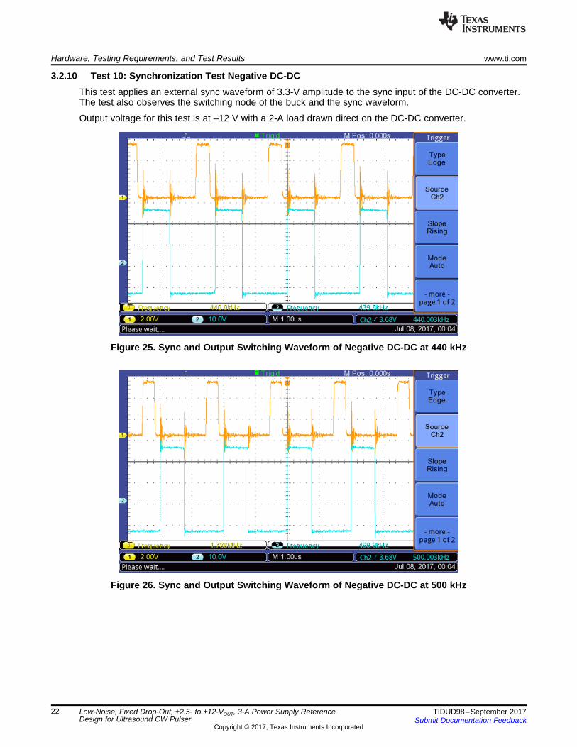
3.2.10 Test 10: Synchronization Test Negative DC-DCThis test applies an external sync waveform of 3.3-V amplitude to the sync input of the DC-DC converter.The test also observes the switching node of the buck and the sync waveform.
Output voltage for this test is at –12 V with a 2-A load drawn direct on the DC-DC converter.
Figure 25. Sync and Output Switching Waveform of Negative DC-DC at 440 kHz
Figure 26. Sync and Output Switching Waveform of Negative DC-DC at 500 kHz
Low-Noise, Fixed Drop-Out, ±2.5- to ±12-VOUT, 3-A Power Supply ReferenceDesign for Ultrasound CW Pulser
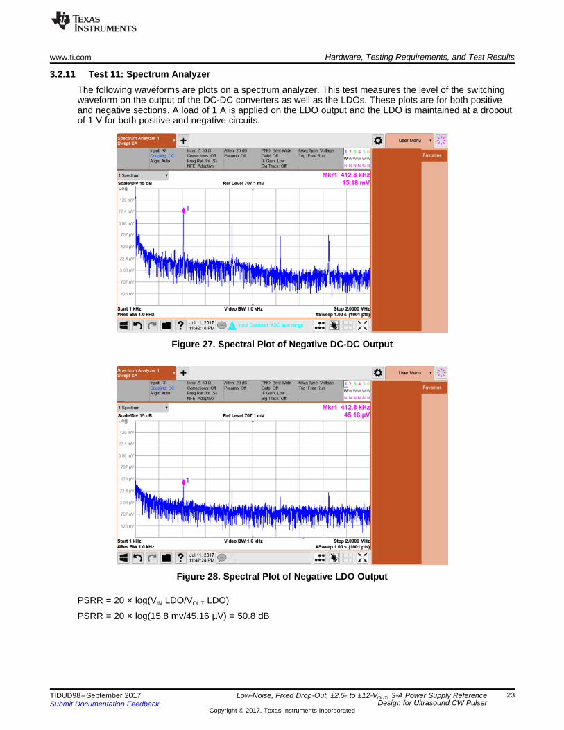
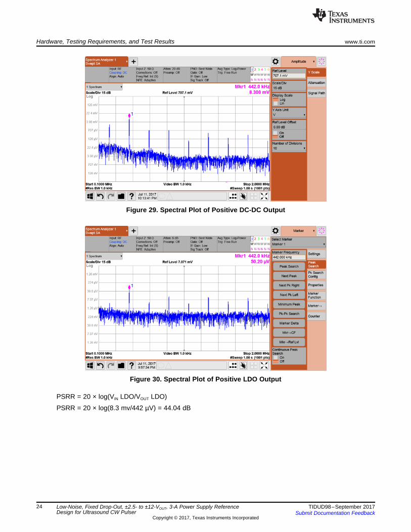
3.2.11 Test 11: Spectrum AnalyzerThe following waveforms are plots on a spectrum analyzer. This test measures the level of the switchingwaveform on the output of the DC-DC converters as well as the LDOs. These plots are for both positiveand negative sections. A load of 1 A is applied on the LDO output and the LDO is maintained at a dropoutof 1 V for both positive and negative circuits.
Low-Noise, Fixed Drop-Out, ±2.5- to ±12-VOUT, 3-A Power Supply ReferenceDesign for Ultrasound CW Pulser
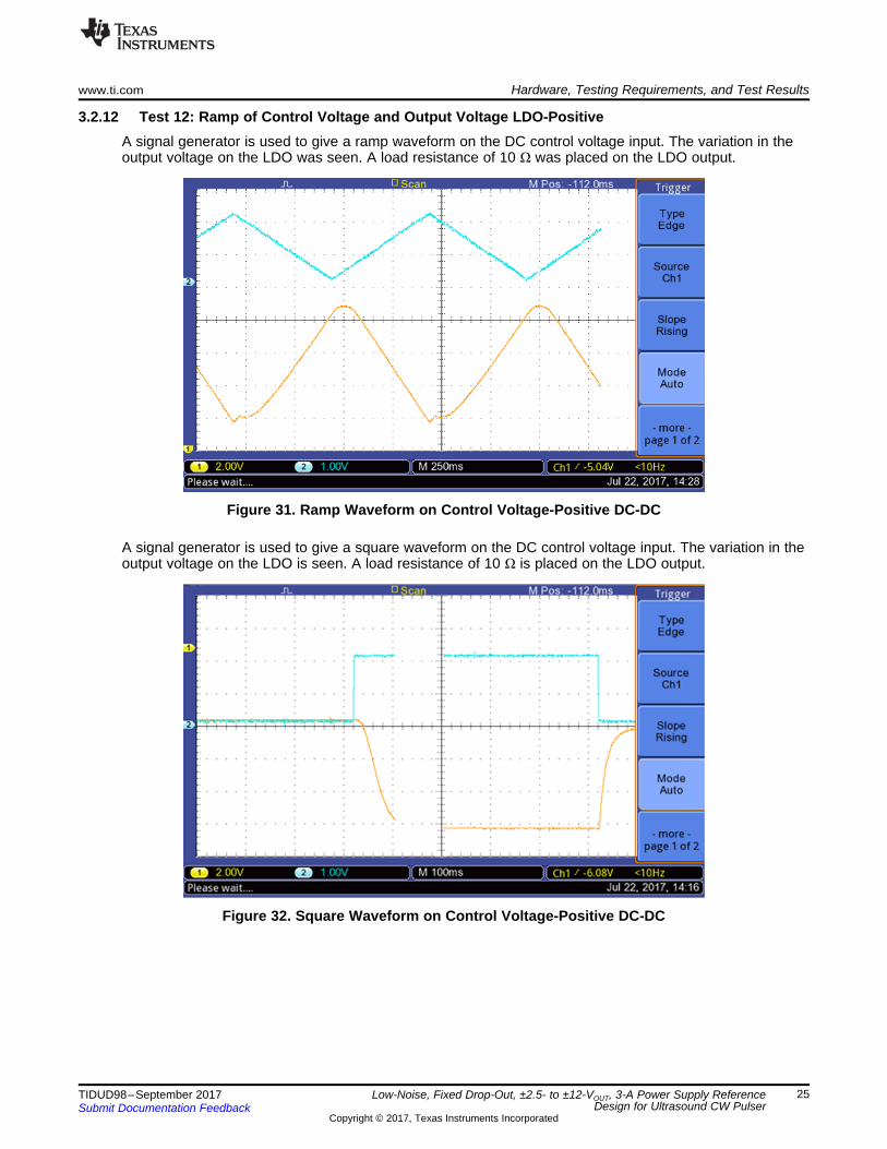
3.2.12 Test 12: Ramp of Control Voltage and Output Voltage LDO-PositiveA signal generator is used to give a ramp waveform on the DC control voltage input. The variation in theoutput voltage on the LDO was seen. A load resistance of 10 Ω was placed on the LDO output.
Figure 31. Ramp Waveform on Control Voltage-Positive DC-DC
A signal generator is used to give a square waveform on the DC control voltage input. The variation in theoutput voltage on the LDO is seen. A load resistance of 10 Ω is placed on the LDO output.
Figure 32. Square Waveform on Control Voltage-Positive DC-DC
Low-Noise, Fixed Drop-Out, ±2.5- to ±12-VOUT, 3-A Power Supply ReferenceDesign for Ultrasound CW Pulser
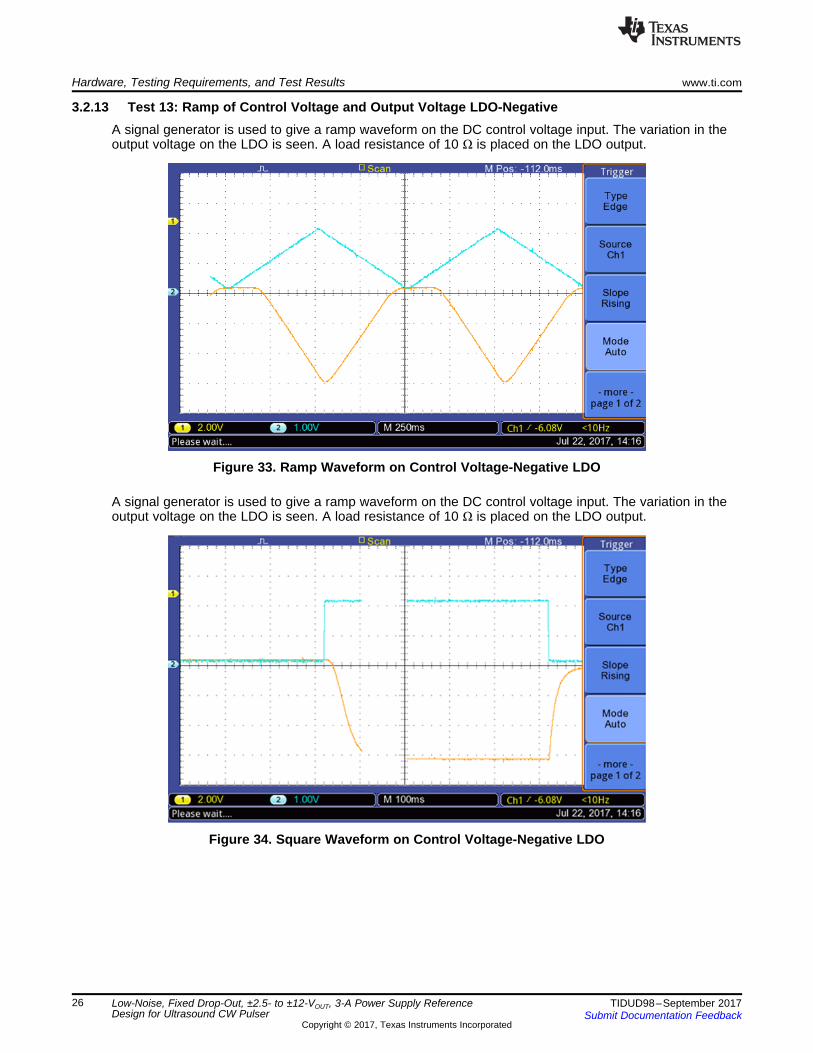
3.2.13 Test 13: Ramp of Control Voltage and Output Voltage LDO-NegativeA signal generator is used to give a ramp waveform on the DC control voltage input. The variation in theoutput voltage on the LDO is seen. A load resistance of 10 Ω is placed on the LDO output.
Figure 33. Ramp Waveform on Control Voltage-Negative LDO
A signal generator is used to give a ramp waveform on the DC control voltage input. The variation in theoutput voltage on the LDO is seen. A load resistance of 10 Ω is placed on the LDO output.
Figure 34. Square Waveform on Control Voltage-Negative LDO
Low-Noise, Fixed Drop-Out, ±2.5- to ±12-VOUT, 3-A Power Supply ReferenceDesign for Ultrasound CW Pulser
4 Design Files
4.1 SchematicsTo download the schematics, see the design files at TIDA-01458.
4.2 Bill of MaterialsTo download the bill of materials (BOM), see the design files at TIDA-01458.
4.3 PCB Layout Recommendations
4.3.1 Layout PrintsTo download the layer plots, see the design files at TIDA-01458.
4.4 Altium ProjectTo download the Altium project files, see the design files at TIDA-01458.
4.5 Gerber FilesTo download the Gerber files, see the design files at TIDA-01458.
4.6 Assembly DrawingsTo download the assembly drawings, see the design files at TIDA-01458.
5 Related DocumentationThis reference design did not use any related documentation.
5.1 TrademarksAll trademarks are the property of their respective owners.
6 About the AuthorSANJAY DIXIT is a system architect in the Industrial Systems-Medical Healthcare and Fitness Sector atTexas Instruments, where he is responsible for specifying reference designs.
IMPORTANT NOTICE FOR TI DESIGN INFORMATION AND RESOURCES
Texas Instruments Incorporated (‘TI”) technical, application or other design advice, services or information, including, but not limited to,reference designs and materials relating to evaluation modules, (collectively, “TI Resources”) are intended to assist designers who aredeveloping applications that incorporate TI products; by downloading, accessing or using any particular TI Resource in any way, you(individually or, if you are acting on behalf of a company, your company) agree to use it solely for this purpose and subject to the terms ofthis Notice.TI’s provision of TI Resources does not expand or otherwise alter TI’s applicable published warranties or warranty disclaimers for TIproducts, and no additional obligations or liabilities arise from TI providing such TI Resources. TI reserves the right to make corrections,enhancements, improvements and other changes to its TI Resources.You understand and agree that you remain responsible for using your independent analysis, evaluation and judgment in designing yourapplications and that you have full and exclusive responsibility to assure the safety of your applications and compliance of your applications(and of all TI products used in or for your applications) with all applicable regulations, laws and other applicable requirements. Yourepresent that, with respect to your applications, you have all the necessary expertise to create and implement safeguards that (1)anticipate dangerous consequences of failures, (2) monitor failures and their consequences, and (3) lessen the likelihood of failures thatmight cause harm and take appropriate actions. You agree that prior to using or distributing any applications that include TI products, youwill thoroughly test such applications and the functionality of such TI products as used in such applications. TI has not conducted anytesting other than that specifically described in the published documentation for a particular TI Resource.You are authorized to use, copy and modify any individual TI Resource only in connection with the development of applications that includethe TI product(s) identified in such TI Resource. NO OTHER LICENSE, EXPRESS OR IMPLIED, BY ESTOPPEL OR OTHERWISE TOANY OTHER TI INTELLECTUAL PROPERTY RIGHT, AND NO LICENSE TO ANY TECHNOLOGY OR INTELLECTUAL PROPERTYRIGHT OF TI OR ANY THIRD PARTY IS GRANTED HEREIN, including but not limited to any patent right, copyright, mask work right, orother intellectual property right relating to any combination, machine, or process in which TI products or services are used. Informationregarding or referencing third-party products or services does not constitute a license to use such products or services, or a warranty orendorsement thereof. Use of TI Resources may require a license from a third party under the patents or other intellectual property of thethird party, or a license from TI under the patents or other intellectual property of TI.TI RESOURCES ARE PROVIDED “AS IS” AND WITH ALL FAULTS. TI DISCLAIMS ALL OTHER WARRANTIES ORREPRESENTATIONS, EXPRESS OR IMPLIED, REGARDING TI RESOURCES OR USE THEREOF, INCLUDING BUT NOT LIMITED TOACCURACY OR COMPLETENESS, TITLE, ANY EPIDEMIC FAILURE WARRANTY AND ANY IMPLIED WARRANTIES OFMERCHANTABILITY, FITNESS FOR A PARTICULAR PURPOSE, AND NON-INFRINGEMENT OF ANY THIRD PARTY INTELLECTUALPROPERTY RIGHTS.TI SHALL NOT BE LIABLE FOR AND SHALL NOT DEFEND OR INDEMNIFY YOU AGAINST ANY CLAIM, INCLUDING BUT NOTLIMITED TO ANY INFRINGEMENT CLAIM THAT RELATES TO OR IS BASED ON ANY COMBINATION OF PRODUCTS EVEN IFDESCRIBED IN TI RESOURCES OR OTHERWISE. IN NO EVENT SHALL TI BE LIABLE FOR ANY ACTUAL, DIRECT, SPECIAL,COLLATERAL, INDIRECT, PUNITIVE, INCIDENTAL, CONSEQUENTIAL OR EXEMPLARY DAMAGES IN CONNECTION WITH ORARISING OUT OF TI RESOURCES OR USE THEREOF, AND REGARDLESS OF WHETHER TI HAS BEEN ADVISED OF THEPOSSIBILITY OF SUCH DAMAGES.You agree to fully indemnify TI and its representatives against any damages, costs, losses, and/or liabilities arising out of your non-compliance with the terms and provisions of this Notice.This Notice applies to TI Resources. Additional terms apply to the use and purchase of certain types of materials, TI products and services.These include; without limitation, TI’s standard terms for semiconductor products http://www.ti.com/sc/docs/stdterms.htm), evaluationmodules, and samples (http://www.ti.com/sc/docs/sampterms.htm).