Int. Journal of Electrical & Electronics Engg. Vol. 2, Spl. Issue 1 (2015) e-ISSN: 1694-2310 | p-ISSN: 1694-2426 Low Power and Area Efficient Multiplier Layout using Transmission Gate Sahil Gargi ME Student (ECE) National Institute of Technical Teachers’ Training & Research Chandigarh, India -160019 [email protected]Abstract: This paper proposes the design and implementation of a 2-bit multiplier using fully automatic design and semi- custom design. Any digital signal processor has adder and multiplier in its core unit. Low power and high speed mac units are in high demand and therefore make a significant place in today’s vlsi environment. Power consumption of cmos circuits is a major concern in vlsi design. The proposed design is made using transmission gate logicwhich helped in using less number of cmos. The multiplier circuit is first simulated using avlsi cad tool and thus the layout was generated. The proposed circuit is simulated by using 90nm cmos technology with supply voltage of 1.2v. It is found that semi-custom based design produced better results in terms of power dissipation and area. Keywords: Multiplier, VLSI, Transmission Gate, CMOS, Power, Area. 1. INTRODUCTION In most of the VLSI applications arithmetic operations like addition, subtraction, multiplication are commonly used. The time required for multiplication is one of the most dominant factor to evaluate the time needed for instruction cycle of a DSP chip. Performance of a DSP chip is largely limited by its multiplication performance. Demand and popularity of various devices depends on the small silicon area, higher speed, longer battery life and reliability [1]. For VLSI design, emphasis is generally laid on three constraints that is, power, area and delay. Interest has now widely grown in optimizing and minimising the chip area with least power consumption and still maintaining high performance.Statics shows that more than 70% instructions in microprocessor and most of DSP algorithms perform addition and multiplication [2]. Thus a multiplier plays a pivotal role in modern VLSI design and a high speed multiplier with low power consumption is the need of the hour. Minimising the power consumption is still a major concern for designers. Most techniques for saving power involve scaling of the power supply, which resulted in substantial increase in the leakage current. It has been found that there is fundamental connection between computation and power dissipation [3]. A method is proposed to somehow reduce the computation without any loss of information. Thus, with reduced computation, there is a reduction in power consumption in the design process. In this paper a fully automatic design is compared with semi-custom design in terms of all the design constraints. Binary multiplication can be performed using number of techniques. Parallel multiplication uses an array or tree of adders (half or full) to sum the partial products. A n*n multiplier requires, n*(n-2) full adders, n half-adders and n 2 AND gates [4]. Shift and add algorithm was the conventional technique used to implement the design. It involved the basic multiplication principle. The partial products are generated by the multiplication of the multiplicand with one multiplier digit followed by addition of shifted partial products. Traditionally shift and add algorithm has been implemented to design however this is not suitable for VLSI implementation and also from delay point of view[4]. Main advantage of binary multiplication is that the generation of intermediate products are easy [2]. Generally this technique of multiplicationisslow and accumulates a lot of area in hardware. Thus requires more power. With the help of Transmission Gate Logic (TGL) there is reduction in leakage power and leakage current in active mode [5]. TGL has proved to be an attractive alternative to static CMOS designs with respect to area, performance and power consumption [6]. It will improve the overall performance.It is designed by connecting both source to source and drain to drain terminals of NMOS and PMOS transistors [7].This logic style has a great functionality that can reduce the number of transistor counts [8]. A design with a high speed is resulted using a TGL with a reduced transistor count. Thus optimised low power circuit design is obtained. As the NMOS transistor is passing strong ‘0’ signal and PMOS transistors passes strong ‘1’ signal towards the output, the both transistors are turn on/off by an enable signal [7].Inverter followed by Transmission gate structure appears in many CMOS circuit design [9].The multiplier is constructed using AND gates and half adder. The half adder is made using transmission gate which is made using EX-OR and AND gates. The multiplier is schematised by DSCH3.1 CAD tool and its layout is generated using CMOS 90nm technology in Microwind 3.1 CAD tool [10]. 2. MULTIPLIER DESIGN This paper presents design approach for a 2-bit multiplier. Two types of multiplier designs are proposed here using Ex-OR and AND gates. A 2-bit multiplier will have a1, a0, b1, b0 as inputs and z3, z2, z1, z0 as outputs. The truth table is shown in Table 1. Table 1: Truth table of 2-bit multiplier Inputs Outputs a1 a0 b1 b0 z3 z2 z1 z0 0 0 0 0 0 0 0 1 0 0 1 0 0 0 1 1 0 1 0 0 0 1 0 1 1 0 1 1 0 1 0 1 1 1 1 1
Low Power and Area Efficient MultiplierLayout using Transmission Gate
Sahil GargiME Student (ECE)
National Institute of Technical Teachers’ Training & Research Chandigarh, [email protected]
Abstract: This paper proposes the design and implementationof a 2-bit multiplier using fully automatic design and semi-custom design. Any digital signal processor has adder andmultiplier in its core unit. Low power and high speed macunits are in high demand and therefore make a significantplace in today’s vlsi environment. Power consumption ofcmos circuits is a major concern in vlsi design. The proposeddesign is made using transmission gate logicwhich helped inusing less number of cmos. The multiplier circuit is firstsimulated using avlsi cad tool and thus the layout wasgenerated. The proposed circuit is simulated by using 90nmcmos technology with supply voltage of 1.2v. It is found thatsemi-custom based design produced better results in terms ofpower dissipation and area.
In most of the VLSI applications arithmetic operations likeaddition, subtraction, multiplication are commonly used.The time required for multiplication is one of the mostdominant factor to evaluate the time needed for instructioncycle of a DSP chip. Performance of a DSP chip is largelylimited by its multiplication performance. Demand andpopularity of various devices depends on the small siliconarea, higher speed, longer battery life and reliability [1].For VLSI design, emphasis is generally laid on threeconstraints that is, power, area and delay. Interest has nowwidely grown in optimizing and minimising the chip areawith least power consumption and still maintaining highperformance.Statics shows that more than 70% instructionsin microprocessor and most of DSP algorithms performaddition and multiplication [2]. Thus a multiplier plays apivotal role in modern VLSI design and a high speedmultiplier with low power consumption is the need of thehour. Minimising the power consumption is still a majorconcern for designers. Most techniques for saving powerinvolve scaling of the power supply, which resulted insubstantial increase in the leakage current. It has beenfound that there is fundamental connection betweencomputation and power dissipation [3]. A method isproposed to somehow reduce the computation without anyloss of information. Thus, with reduced computation, thereis a reduction in power consumption in the design process.In this paper a fully automatic design is compared withsemi-custom design in terms of all the design constraints.
Binary multiplication can be performed using number oftechniques. Parallel multiplication uses an array or tree ofadders (half or full) to sum the partial products. A n*nmultiplier requires, n*(n-2) full adders, n half-adders andn2 AND gates [4]. Shift and add algorithm was theconventional technique used to implement the design. Itinvolved the basic multiplication principle. The partial
products are generated by the multiplication of themultiplicand with one multiplier digit followed by additionof shifted partial products. Traditionally shift and addalgorithm has been implemented to design however this isnot suitable for VLSI implementation and also from delaypoint of view[4]. Main advantage of binary multiplicationis that the generation of intermediate products are easy [2].Generally this technique of multiplicationisslow andaccumulates a lot of area in hardware. Thus requires morepower.
With the help of Transmission Gate Logic (TGL) there isreduction in leakage power and leakage current in activemode [5]. TGL has proved to be an attractive alternative tostatic CMOS designs with respect to area, performance andpower consumption [6]. It will improve the overallperformance.It is designed by connecting both source tosource and drain to drain terminals of NMOS and PMOStransistors [7].This logic style has a great functionality thatcan reduce the number of transistor counts [8]. A designwith a high speed is resulted using a TGL with a reducedtransistor count. Thus optimised low power circuit designis obtained. As the NMOS transistor is passing strong ‘0’signal and PMOS transistors passes strong ‘1’ signaltowards the output, the both transistors are turn on/off byan enable signal [7].Inverter followed by Transmissiongate structure appears in many CMOS circuit design[9].The multiplier is constructed using AND gates and halfadder. The half adder is made using transmission gatewhich is made using EX-OR and AND gates. Themultiplier is schematised by DSCH3.1 CAD tool and itslayout is generated using CMOS 90nm technology inMicrowind 3.1 CAD tool [10].
2. MULTIPLIER DESIGNThis paper presents design approach for a 2-bit multiplier.Two types of multiplier designs are proposed here usingEx-OR and AND gates. A 2-bit multiplier will have a1, a0,b1, b0 as inputs and z3, z2, z1, z0 as outputs. The truthtable is shown in Table 1.
In Fully Automatic (FA) Design approach, the design iscreated using DSCH3.1 CAD tool. DSCH is used tovalidate the architecture of the logic circuit before themicroelectronics design is started [11]. CMOS circuits isused to create AND gate and half-adder.Transmissiongatelogic style of 2-bit multiplier shown in Fig. 1is usedwhich helped in reducing the number of CMOS.
Fig. 1 CMOS design in DSCH
The corresponding simulation or behavior in DSCH tocheck the functionality is shown in Fig. 2.
Fig. 2 Simulation results in DSCH
The layout of the multiplier is generated usingMicrowind3.1 CAD tool by compiling a Verilog file thatwas created in DSCH.Its corresponding simulation resultsalong with power are shown in Fig. 3. And thecorresponding Auto Generated layout is created as shownin Fig. 4.
Fig. 3 Simulation results of FA design
Fig. 4Layout of FA design
In Semi-Custom (SC) Design approach, the layout isdirectly made in Microwind3.1 using MOS generators.Similar to fully automatic design, transmission gatelogicstyle is also used here. But the only difference is that bothNMOS and PMOS are made using this MOS generator.That is if somehow computation could be implementedwithout any loss of information, then energy required by itcould be potentially reduced by a large amount [3]. Themain advantage of using semi-custom design approach isthe reduction in computations without any loss ofinformation. With reduced computation, the chip area andpower consumption is optimised to a significant level. Thelayout of 2-bit multiplier using semi-custom design isshown in Fig. 5. It can be clearly seen the semi-customdesign occupies less chip area as compared to fullyautomatic.
The simulation results for the SC design are shown in Fig.6. The Simulation results of both designs appear to besimilar implying that there is no loss of information insemi-custom approach. However the power consumed insemi-custom is quite low as compared to fully automaticdesign.
Fig. 6Simulation results of SC design
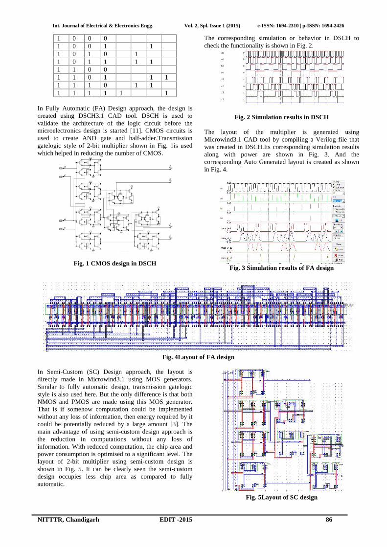
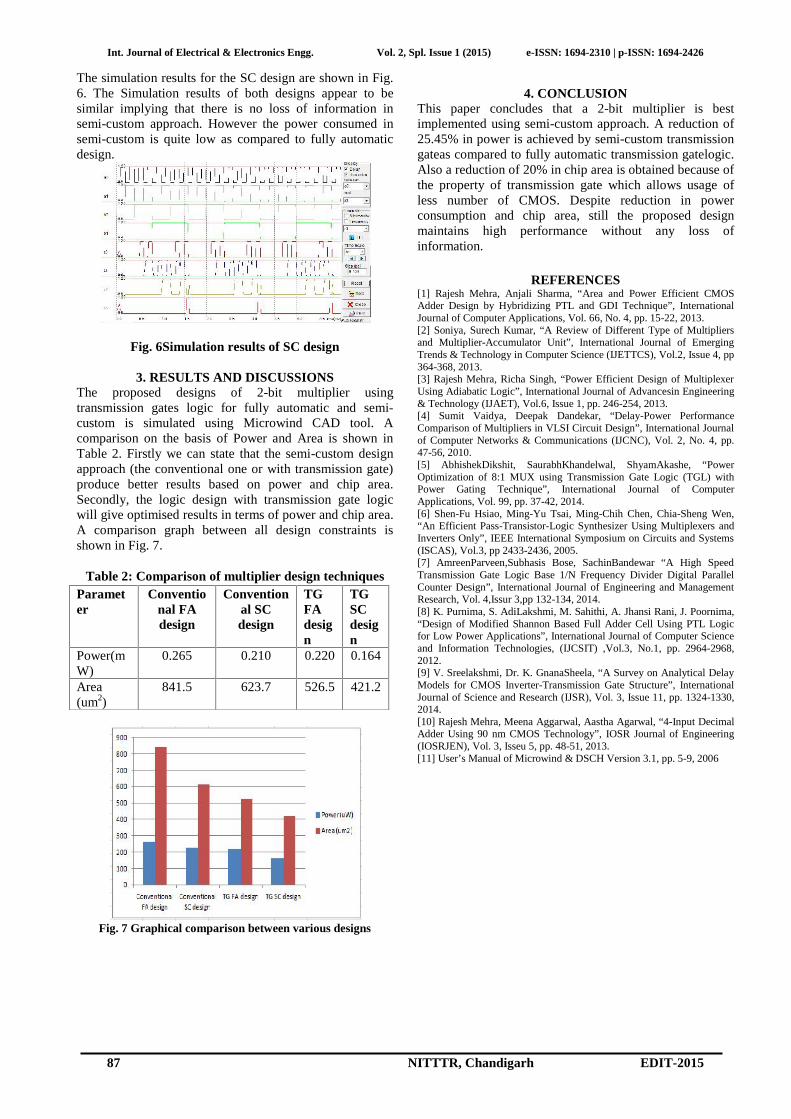
3. RESULTS AND DISCUSSIONSThe proposed designs of 2-bit multiplier usingtransmission gates logic for fully automatic and semi-custom is simulated using Microwind CAD tool. Acomparison on the basis of Power and Area is shown inTable 2. Firstly we can state that the semi-custom designapproach (the conventional one or with transmission gate)produce better results based on power and chip area.Secondly, the logic design with transmission gate logicwill give optimised results in terms of power and chip area.A comparison graph between all design constraints isshown in Fig. 7.
Table 2: Comparison of multiplier design techniques
Fig. 7 Graphical comparison between various designs
4. CONCLUSIONThis paper concludes that a 2-bit multiplier is bestimplemented using semi-custom approach. A reduction of25.45% in power is achieved by semi-custom transmissiongateas compared to fully automatic transmission gatelogic.Also a reduction of 20% in chip area is obtained because ofthe property of transmission gate which allows usage ofless number of CMOS. Despite reduction in powerconsumption and chip area, still the proposed designmaintains high performance without any loss ofinformation.
REFERENCES[1] Rajesh Mehra, Anjali Sharma, “Area and Power Efficient CMOSAdder Design by Hybridizing PTL and GDI Technique”, InternationalJournal of Computer Applications, Vol. 66, No. 4, pp. 15-22, 2013.[2] Soniya, Surech Kumar, “A Review of Different Type of Multipliersand Multiplier-Accumulator Unit”, International Journal of EmergingTrends & Technology in Computer Science (IJETTCS), Vol.2, Issue 4, pp364-368, 2013.[3] Rajesh Mehra, Richa Singh, “Power Efficient Design of MultiplexerUsing Adiabatic Logic”, International Journal of Advancesin Engineering& Technology (IJAET), Vol.6, Issue 1, pp. 246-254, 2013.[4] Sumit Vaidya, Deepak Dandekar, “Delay-Power PerformanceComparison of Multipliers in VLSI Circuit Design”, International Journalof Computer Networks & Communications (IJCNC), Vol. 2, No. 4, pp.47-56, 2010.[5] AbhishekDikshit, SaurabhKhandelwal, ShyamAkashe, “PowerOptimization of 8:1 MUX using Transmission Gate Logic (TGL) withPower Gating Technique”, International Journal of ComputerApplications, Vol. 99, pp. 37-42, 2014.[6] Shen-Fu Hsiao, Ming-Yu Tsai, Ming-Chih Chen, Chia-Sheng Wen,“An Efficient Pass-Transistor-Logic Synthesizer Using Multiplexers andInverters Only”, IEEE International Symposium on Circuits and Systems(ISCAS), Vol.3, pp 2433-2436, 2005.[7] AmreenParveen,Subhasis Bose, SachinBandewar “A High SpeedTransmission Gate Logic Base 1/N Frequency Divider Digital ParallelCounter Design”, International Journal of Engineering and ManagementResearch, Vol. 4,Issur 3,pp 132-134, 2014.[8] K. Purnima, S. AdiLakshmi, M. Sahithi, A. Jhansi Rani, J. Poornima,“Design of Modified Shannon Based Full Adder Cell Using PTL Logicfor Low Power Applications”, International Journal of Computer Scienceand Information Technologies, (IJCSIT) ,Vol.3, No.1, pp. 2964-2968,2012.[9] V. Sreelakshmi, Dr. K. GnanaSheela, “A Survey on Analytical DelayModels for CMOS Inverter-Transmission Gate Structure”, InternationalJournal of Science and Research (IJSR), Vol. 3, Issue 11, pp. 1324-1330,2014.[10] Rajesh Mehra, Meena Aggarwal, Aastha Agarwal, “4-Input DecimalAdder Using 90 nm CMOS Technology”, IOSR Journal of Engineering(IOSRJEN), Vol. 3, Isseu 5, pp. 48-51, 2013.[11] User’s Manual of Microwind & DSCH Version 3.1, pp. 5-9, 2006