Page 1
JOURNAL OF SEMICONDUCTOR TECHNOLOGY AND SCIENCE, VOL.14, NO.1, FEBRUARY, 2014 http://dx.doi.org/10.5573/JSTS.2014.14.1.109
Manuscript received Jul. 18, 2013; accepted Oct. 22, 2013
Sung Kyun Kwan University, Electronic and Electrical Engineering 300
Cheoncheon-dong Suwon 440-746 Korea, Republic of
E-mail: [email protected]
Low-Power and High-Efficiency Class-D Audio
Amplifier Using Composite Interpolation Filter for
Digital Modulators
Minchul Kang, Hyungchul Kim, Jehyeon Gu, Wonseob Lim, Junghyun Ham, Hearyun Jung,
and Youngoo Yang*
Abstract—This paper presents a high-efficiency
digital class-D audio amplifier using a composite
interpolation filter for portable audio devices. The
proposed audio amplifier is composed of an
interpolation filter, a delta-sigma modulator, and a
class-D output stage. To reduce power consumption,
the designed interpolation filter has an optimized
composite structure that uses a direct-form
symmetric and Lagrange FIR filters. Compared to
the filters with homogeneous structures, the hardware
cost and complexity are reduced by about half by the
optimization. The coefficients of the digital delta-
sigma modulator are also optimized for low power
consumption. The class-D output stage has gate driver
circuits to reduce shoot-through current. The
implemented class-D audio amplifier exhibited a high
efficiency of 87.8 % with an output power of 57 mW
at a load impedance of 16 Ω and a power supply
voltage of 1.8 V. An outstanding signal-to-noise ratio
of 90 dB and a total harmonic distortion plus noise of
0.03 % are achieved for a single-tone input signal
with a frequency of 1 kHz.
Index Terms—Audio amplifier, digital class-D
amplifier, composite interpolation filter, delta-sigma
modulator, dead-time gate driver
I. INTRODUCTION
Interests in high-efficiency audio amplifiers with low
power consumption have been increasing for portable
applications, such as hearing instruments, wireless
headsets, and mobile phones [1]. Since the peak-to-
average ratio (PAR) of an audio signal is 9 to 15 dB,
linear amplifiers such as class-A or class–AB amplifiers
have significantly reduced efficiency for the backed-off
region from the peak output power and are not suitable
for portable audio systems [2, 3]. Therefore, the class-D
amplifier is preferred for portable applications because
high efficiency can be maintained even at significantly
backed-off power levels [4].
The architectures of the class-D amplifier can be
classified into two types: 1) one based on pulse width
modulation (PWM) method [5, 6] and 2) another based
on pulse density modulation (PDM) method using a
delta-sigma modulator (DSM) [7]. For an audio amplifier
based on PWM method, a comparator is used to generate
a pulse signal by comparing the input signal and a carrier
signal which has a triangular or saw-tooth waveform.
The carrier signal with a relatively low frequency leads
to harmonics issues [5].
Alternatively, the class-D amplifiers based on PDM
method using a DSM have a little lower power efficiency
due to the relatively fast clock speed but have more
linear output characteristics that can be achieved through
the proper selection of oversampling ratio (OSR) and
loop filter parameters [8]. The audio amplifiers based on
PDM method are more suitable for digital audio
Page 2
110 MINCHUL KANG et al : LOW-POWER AND HIGH-EFFICIENCY CLASS-D AUDIO AMPLIFIER USING COMPOSITE …
applications, since they have digital input.
In this paper, we present a digital class-D audio
amplifier, composed of a 16-bit digital interpolation filter
(IF), a 3rd-order DSM, and a class-D output stage with
gate driver circuits for a reduced shoot-through current.
The IF has a composite structure with direct-form
symmetric and Lagrange finite impulse response (FIR)
filters for low power consumption. In addition, the noise
gain of the DSM for a voice bandwidth of up to 8 kHz is
optimized to minimize the current consumption.
II. DESIGN OF DIGITAL CLASS-D AUDIO
AMPLIFIER
Digital class-D audio amplifiers commonly comprise
an IF, a modulator, and a class-D output stage. A typical
structure of the designed digital class-D audio amplifier
is shown in Fig. 1. As the 16-bit pulse-coded modulation
(PCM) signal is applied to the IF, the filter oversamples
the input signal with an OSR of 32. Then, the DSM
converts the oversampled PCM signal to the 1-bit PDM
signal and delivers it to the class-D output sage.
1. Composite Structure of the IF
An FIR filter is a common type of IF. A cascaded 5-
stage IF is optimized with a composite structure for low
power consumption, as shown in Fig. 2. Using multiple
cascaded stages, a digital filter with a high OSR can have
relatively mitigated hardware complexity, compared to
the high-order single-stage filters for similar cut-off
characteristics [9]. Due to the OSR of 32, the output
digital signal of the IF has a sampling frequency of 1.024
MHz while that of the input is 32 kHz.
A 5-stage composite structure using a 14th-order
direct-form symmetric FIR filter as the first stage and a
Lagrange FIR filter for the following 4 stages is used to
optimize power consumption and cost. The first stage has
a high order of 14 to sharply cut off the image signal that
is generated by the signal sampling.
A structure of the designed direct-form symmetric FIR
filter for the first stage is shown in Fig. 3(a). Since the
direct-form symmetric structure has been adopted instead
of just a direct form, the hardware cost decreases by
approximately half. Additionally, the following stages
can have rather simple structure, which can reduce the
Fig. 1. A structure of the digital class-D audio amplifier based
on PDM method.
Fig. 2. A structure of the proposed 5-stage composite
interpolation filter.
(a)
(b)
Fig. 3. Schematic diagrams of the IF stages (a) 14th-order
direct-form symmetric FIR filter for the first stage, (b) cascaded
Lagrange FIR filter for the 2nd to 5th-stages.
Page 3
JOURNAL OF SEMICONDUCTOR TECHNOLOGY AND SCIENCE, VOL.14, NO.1, FEBRUARY, 2014 111
power consumption caused by the higher clock speed.
Table 1 shows the coefficients based on 16-bit finite
length word for the 14th-order direct-form symmetric FIR
filter.
A Lagrange filter, as shown in Fig. 3(b), is adopted for
the 2nd to 5th stages. The 2nd stage has 2nd-order structure,
and the other three stages have 1st-order structure. The
amplitude response of the designed 5-stage IF is plotted
in Fig. 4. Low ripple characteristics within ±0.09 dB are
obtained up to a given audio bandwidth of 8 kHz.
The characteristics of the proposed composite IF are
compared to the IF filters with homogeneous structures,
which are optimized to have performance similar to that
of the proposed composite IF structure, as shown in
Table 2. In comparison, the hardware cost is reduced by
about half due to the optimized composite structure.
Furthermore, the simulated power consumption
simulated using Design Compiler is as low as 1.33 µW.
2. Digital DSM
The digital DSM is composed of integrators, a
quantizer, and feedback loops, as shown in Fig. 5. The
coefficients, which are connected to each node,
determine the transfer characteristics and the out-band
noise gain [10]. The extracted coefficients are presented
in Table 3.
The feedback loops reduce quantization noise in the
low frequency region for noise shaping characteristics
[11]. The coefficients at each node and order of the DSM
are optimized for the audio band of 8 kHz for better noise
shape. The designed DSM transforms the 16-bit input
signal into a 1-bit PDM signal with a clock frequency of
1.024 MHz.
A power consumption of 13 µW was achieved with the
designed modulator, including the composite IF, in
simulations using Design Compiler. Fig. 6 shows the
measured output power spectral density (PSD) of the
designed modulator, including the IF and DSM. As
shown in Fig. 7, the measured THD+N of the designed
modulator is lower than -72 dB. The circuits were
implemented on a vertex-5 FPGA board. Measurements
Table 2. Comparison of the proposed IF to the IF’s with
homogeneous structures
direct-form
symmetric Lagrange This work
Ripple (dB) @ 0 Hz-8 kHz
±0.11 ±0.09 ±0.09
Attenuation (dB)
@ 32 kHz -66 -76 -66
Tap/multiplier/adder 40/40
/34
14/84
/78
16/24
/25
Power (µW) 5.21 3.6 1.33
*fs: 1.024 MHz, VDD: 1.8 V with 0.18 µm process
Table 3. The extracted coefficients for the DSM
Coefficients Value Coefficient Value
a1 1/24+1/26 c1 1/23+1/25
a2 1/23+1/25 c2 1/22+1/23
a3 1/22+1/24 c3 1
b1 1/24+1/26 g1 1/28
* b2=b3=b4=0
Fig. 5. A schematic diagram of the designed DSM.
Table 1. Coefficients for the 14th-order direct-form symmetric
FIR filter
Coefficient Value
C1 -0.009796142578125
C2 -0.000335693359375
C3 0.034820556640625
C4 -0.0152587890625
C5 -0.095367431640625
C6 0.10394287109375
C7 0.4795989990234375
Fig. 4. Amplitude response of the designed filter.
Page 4
112 MINCHUL KANG et al : LOW-POWER AND HIGH-EFFICIENCY CLASS-D AUDIO AMPLIFIER USING COMPOSITE …
were done using a Chipscope.
For an input signal of a 1-kHz sine wave, which has a
full-scale (FS) magnitude of 0.8, an outstanding SNR of
90 dB was achieved. As the out-band noise gain of the
DSM becomes larger, the allowable scale of the input
signal should be smaller for unconditional stability. Table
4 shows the maximum stable input scale and THD+N
characteristics according to the out-band noise gain of
the DSM. The designed modulator has an out-band noise
gain of 1.2 and operates with a reasonable maximum
stable input signal scale of 0.897.
3. Full-bridge class-D output stage
For low even-order harmonic distortion, full-bridge
class-D structure is adopted as the output stage of the
amplifier (see Fig. 1). The full-bridge structure has low
even-order harmonic distortion and does not require a
DC blocking capacitor. After passing the low-pass filter
at the output of the amplifier, the in-band audio signal
can be restored.
For class-D amplifiers, efficiency degradation comes
from switching loss, conduction loss, and shoot-through
current loss [12]. The shoot-through current loss can be
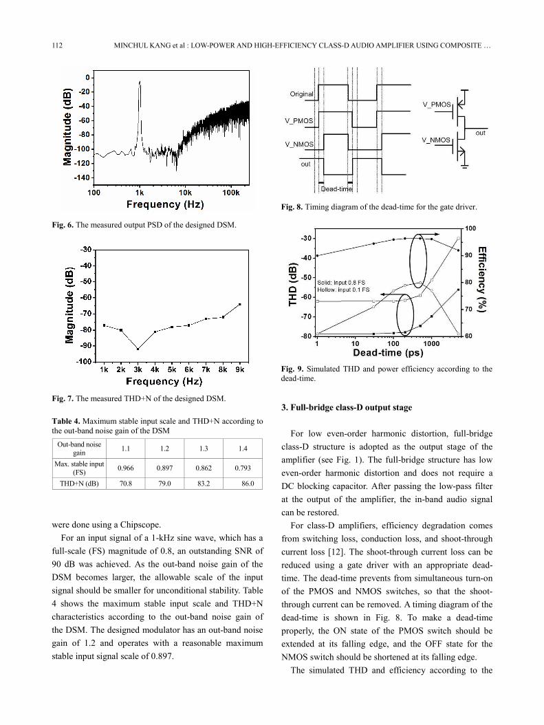
reduced using a gate driver with an appropriate dead-
time. The dead-time prevents from simultaneous turn-on
of the PMOS and NMOS switches, so that the shoot-
through current can be removed. A timing diagram of the
dead-time is shown in Fig. 8. To make a dead-time
properly, the ON state of the PMOS switch should be
extended at its falling edge, and the OFF state for the
NMOS switch should be shortened at its falling edge.
The simulated THD and efficiency according to the
Fig. 6. The measured output PSD of the designed DSM.
Fig. 7. The measured THD+N of the designed DSM.
Table 4. Maximum stable input scale and THD+N according to
the out-band noise gain of the DSM
Out-band noise gain
1.1 1.2 1.3 1.4
Max. stable input
(FS) 0.966 0.897 0.862 0.793
THD+N (dB) 70.8 79.0 83.2 86.0
Fig. 8. Timing diagram of the dead-time for the gate driver.
Fig. 9. Simulated THD and power efficiency according to the
dead-time.
Page 5
JOURNAL OF SEMICONDUCTOR TECHNOLOGY AND SCIENCE, VOL.14, NO.1, FEBRUARY, 2014 113
dead-time are shown in Fig. 9. As the dead-time
increases, the power efficiency and THD increase. If the
dead-time becomes too long, the power efficiency
decreases due to the decreased output power. Before
having too much of an increase in THD, a dead-time of
150 ps was chosen for optimal efficiency improvement.
Since the peak-to-average ratio (PAR) of the audio
signal is about 10 dB [13], the efficiency at an output
level of 0.1 FS significantly improves from an initial
value of around 60 % to around 80 %.
III. EXPERIMENTAL RESULTS
The designed IF and DSM are implemented using a
vertex-5 FPGA board and the full-bridge class-D output
stage including the gate driver was fabricated using
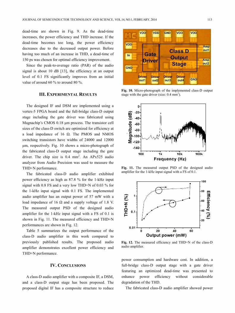
Magnachip’s CMOS 0.18 µm process. The transistor cell
sizes of the class-D switch are optimized for efficiency at
a load impedance of 16 Ω. The PMOS and NMOS
switching transistors have widths of 24000 and 12000
µm, respectively. Fig. 10 shows a micro-photograph of
the fabricated class-D output stage including the gate
driver. The chip size is 0.4 mm2. An APx525 audio
analyzer from Audio Precision was used to measure the
THD+N performance.
The fabricated class-D audio amplifier exhibited
power efficiency as high as 87.8 % for the 1-kHz input
signal with 0.8 FS and a very low THD+N of 0.03 % for
the 1-kHz input signal with 0.1 FS. The implemented
audio amplifier has an output power of 57 mW with a
load impedance of 16 Ω and a supply voltage of 1.8 V.
The measured output PSD of the designed audio
amplifier for the 1-kHz input signal with a FS of 0.1 is
shown in Fig. 11. The measured efficiency and THD+N
performances are shown in Fig. 12.
Table 5 summarizes the output performance of the
class-D audio amplifier in this work compared to
previously published results. The proposed audio
amplifier demonstrates excellent power efficiency and
THD+N performance.
IV. CONCLUSIONS
A class-D audio amplifier with a composite IF, a DSM,
and a class-D output stage has been proposed. The
proposed digital IF has a composite structure to reduce
power consumption and hardware cost. In addition, a
full-bridge class-D output stage with a gate driver
featuring an optimized dead-time was presented to
enhance power efficiency without considerable
degradation of the THD.
The fabricated class-D audio amplifier showed power
Fig. 10. Micro-photograph of the implemented class-D output
stage with the gate driver (size: 0.4 mm2).
.
Fig. 11. The measured output PSD of the designed audio
amplifier for the 1-kHz input signal with a FS of 0.1.
Fig. 12. The measured efficiency and THD+N of the class-D
audio amplifier.
Page 6
114 MINCHUL KANG et al : LOW-POWER AND HIGH-EFFICIENCY CLASS-D AUDIO AMPLIFIER USING COMPOSITE …
efficiency as high as 87.8 % and low THD+N of 0.03 %
for a 1-kHz sinusoidal input signal. It has an output
power of 57 mW with a load impedance of 16 Ω and a
supply voltage of 1.8 V.
ACKNOWLEDGMENTS
This work was supported by the National Research
Foundation of Korea under Grant 2012-003485.
REFERENCES
[1] V. Adrian, J. S. Chang, and B. H. Gwee, “A low-
voltage micropower digital class-D amplifier
modulator for hearing aids,” IEEE Trans. Circuits
Syst. Ⅰ, Reg. Papers, vol. 56, no.2, pp. 337 - 349,
Feb. 2009.
[2] K. Kang, J. Roh, Y. Choi, H. Roh, H. Nam, and S.
Lee, “Class-D audio amplifier using 1-bit fourth-
order delta-sigma modulation,” IEEE Trans.
Circuits Syst. Ⅱ, Exp. Briefs, vol. 55, no. 8, pp.
728-732. Aug. 2008.
[3] K. Kim, J. Kim and C. Park, “Efficiency
improvement of HBT class E power amplifier by
tuning-out input capacitance,” J. Semicond.
Technol. Sci., vol. 7, no. 4, pp. 274-280. Dec. 2007.
[4] T. Ge and J. S. Chang, “Bang-Bang control Class D
amplifiers: Power-supply noise,” IEEE Trans.
Circuits Syst. Ⅱ, Briefs, vol. 55, no. 8, pp. 723-727.
Aug. 2008.
[5] M. T. Tan, J. S. Chang, H. C. Chua, and B. H.
Gwee, “An investigation into the parameters
affecting total harmonic distortion in low-voltage
low-power Class-D amplifiers,” IEEE Trans.
Circuits Syst. Ⅰ, Fundam. Theory Appl., vol. 50,
no. 10, pp. 1304-1315. Oct. 2003.
[6] M. Berkhout, “Integrated 200-W class-D audio
amplifier,” J. Solid-State Circuits, vol. 38, no. 7, pp.
1198-1206. Jul. 2003.
[7] B. H. Leung and S. Sutarja, “Multi-bit sigma-delta
A/D converter incorporating a novel class of
dynamic element matching techniques,” IEEE
Trans. Circuits Syst. Ⅱ, vol. 39, no. 1, pp. 35-51.
Jan. 1992.
[8] Karsten Nielsen, “Audio power amplifier
techniques with energy efficient power
conversion,” Ph. D. Thesis, Department of Applied
Electronics, Building 451 Technical University of
Denmark, April. 1992.
[9] B. P. Brandt and B. A. Wooley, “A low-power,
area-efficient digital filter for decimation and
interpolation,” IEEE J. Solid-State Circuits, vol. 29,
no. 6, pp. 679-687. Jun. 1994.
[10] J. Shin, J. Kim, S. Kim and H. Shin, “A delta-
sigma fractional-N frequency synthesizer for quad-
band multi-standard mobile broadcasting tuners in
0.18-um CMOS,” J. Semicond. Technol. Sci., vol. 7,
no. 4, pp. 267-273. Dec. 2007.
[11] R. Schreier and G. C. Temes, Understanding delta-
sigma data converters, New York: Wiley-IEEE
Press, 2004.
[12] J. Varona, A. A. Hamoui, and K. Martin, “A low
voltage fully-monolithic delta-sigma based Class-D
Table 5. Performance comparison
Parameter [2] [11] [14] [15] This work
Modulator architecture Analog ∆Σ Digital ∆Σ Analog PWM* Analog PWM** Digital ∆Σ
Process (µm) CMOS 0.18 CMOS 0.18 CMOS 0.5 CMOS 0.5 CMOS 0.18
Power supply (V) 3.0 1.8 2.7 2.5 1.8
Pout (mW) N/A N/A 250 450 57
Sampling frequency (MHz)
3.2 N/A 0.45 0.2 1.024
Load impedance (Ω)
32 36 8 8 16
Peak SNR (dB) 98.5 71 92 80 90
THD+N (%) 0.022 0.07 (THD) 0.05 0.07 0.03
Efficiency (%) 77 79 90 92 87.8
Bandwidth (kHz) 20 20 20 20 8
* Sliding mode control ** Rectangular-wave delta modulator
Page 7
JOURNAL OF SEMICONDUCTOR TECHNOLOGY AND SCIENCE, VOL.14, NO.1, FEBRUARY, 2014 115
audio amplifier,” Proc. Eur. Solid-State Circuits
Conf. (ESSCIRC), pp. 545-548. Sep. 2003.
[13] R. Becker and W. H. Groeneweg, “An audio
amplifier providing up to 1 Watt in standard digital
90-nm CMOS,” IEEE J. Solid-State Circuits, vol.
41, no. 7, pp. 1648-1653. Jul. 2006.
[14] M. A. Rojas-Gonzalez and E. Sanchez-Sinencio,
“Low-power high-efficiency class D audio power
amplifiers,” IEEE J. Solid-State Circuits, vol. 44,
no. 12, pp. 3272-3284. Dec. 2009.
[15] S. C. Li, V. C. C. Lin, K. Nandhasri, and J.
Ngarmnil, “New high-efficiency 2.5 V/0.45 W
RWDM Class-D audio amp for portable consumer
electronics,” IEEE Trans. Circuits Syst. Ⅰ, Reg.
Papers, vol. 52, no. 9, pp. 1767-1774. Sep. 2005.
Minchul Kang received the B.S.
degree in the department of
electronic and computer engineering
from Sungkyunkwan University,
Suwan, Korea in 2011. He is
currently working toward the M. S.
degree in the department of electronic and computer
engineering from Sungkyunkwan University. His current
research interests include class-D amplifier, high
efficiency power amplifier, DAC, digital filter and mixed
signal circuit design.
Hyungchul Kim was born in
Chuncheon, Korea, in 1983. He
received the B.S. and M.S. degrees in
electronic and computer engineering
from Sungkyunkwan University,
Suwan, Korea in 2008 and 2010,
respectrively. He is currently working
toward the Ph.D. degree in Sungkyunkwan University.
His research interests include RF power amplifier design,
RFID tag IC design, low-power analog/mixed signal
circuit design and power converter design.
Jehyun Gu received the B.S. degree
in the department of electronic and
computer engineering from Sung-
kyunkwan University, Suwan, Korea
in 2012. He is currently working
toward the M. S. degree in the
department of IT convergence from
Sungkyunkwan University. His current research interests
include audio amplifier modeling, power amplifier,
broadband Doherty power amplifier.
Wonseob Lim received the B.S.
degree in the department of
Electronics and Communication Engi-
neering from Hanyang University,
Ansan, Korea in 2012. He is
currently working toward the M. S.
degree in the department of
electronic and computer engineering from
Sungkyunkwan University. His current research interests
include class-D amplifier, high efficiency power
amplifier, DAC, digital filter and mixed signal circuit
design.
Junghyun Ham was born in Seoul,
Korea, in 1980. He received the M.S.
degree in electrical and computer
engineering from Hanyang Univer-
sity, Seoul, Korea, in 2009 and is
currently working toward the Ph.D.
degree in the department of electronic
and computer engineering from Sungkyunkwan
University, Suwan, Korea. From 2009 to 2011, He was
with LG Electronics, Seoul, Korea, where he was
involved in the development of the high efficient power
amplifier for mobile handset applications. His research
includes high efficient RF transmitters, high-speed DC-
DC converters, and CMOS RF power amplifiers.
Page 8
116 MINCHUL KANG et al : LOW-POWER AND HIGH-EFFICIENCY CLASS-D AUDIO AMPLIFIER USING COMPOSITE …
Hearyun Jung received the B.S.
degree in the department of
electronic engineering from Kwang-
woon University, Seoul, Korea in
2012. She is currently working
toward the M.S. degree in the
department of electronic and computer
engineering from Sungkyunkwan University. Her current
research interests include bias modulator, high efficiency
power amplifier and mixed signal circuit design.
Youngoo Yang was born in Hamyang,
Korea, in 1969. He received the Ph.D.
degree in electrical and electronic
engineering from the Pohang
University of Science and Technology
(Postech), Pohang, Korea, in 2002.
From 2002 to 2005, he was with
Skyworks Solutions Inc., Newbury Park, CA, where he
designed power amplifiers for various cellular handsets.
Since March 2005, he has been with the School of
Information and Communication Engineering, Sungkyun-
kwan University, Suwon, Korea, where he is currently an
associate professor. His research interests include power
amplifier design, RF transmitters, RFIC design,
integrated circuit design for RFID/USN systems, and
modeling of high power amplifiers or devices.