LOW POWER DC-DC CONVERTERS AND A LOW QUIESCENT POWER HIGH PSRR CLASS-D AUDIO AMPLIFIER A Dissertation by JOSELYN TORRES Submitted to the Office of Graduate and Professional Studies of Texas A&M University in partial fulfillment of the requirements for the degree of DOCTOR OF PHILOSOPHY Chair of Committee, EdgarS´anchez-Sinencio Committee Members, Jos´ e Silva-Mart´ ınez Prasad Enjeti C´ esar Malav´ e Head of Department, Chanan Singh December 2013 Major Subject: Electrical Engineering Copyright 2013 Joselyn Torres
Transcript
LOW POWER DC-DC CONVERTERS AND A LOW QUIESCENT POWER
HIGH PSRR CLASS-D AUDIO AMPLIFIER
A Dissertation
by
JOSELYN TORRES
Submitted to the Office of Graduate and Professional Studies ofTexas A&M University
in partial fulfillment of the requirements for the degree of
DOCTOR OF PHILOSOPHY
Chair of Committee, Edgar Sanchez-SinencioCommittee Members, Jose Silva-Martınez
Prasad EnjetiCesar Malave
Head of Department, Chanan Singh
December 2013
Major Subject: Electrical Engineering
Copyright 2013 Joselyn Torres
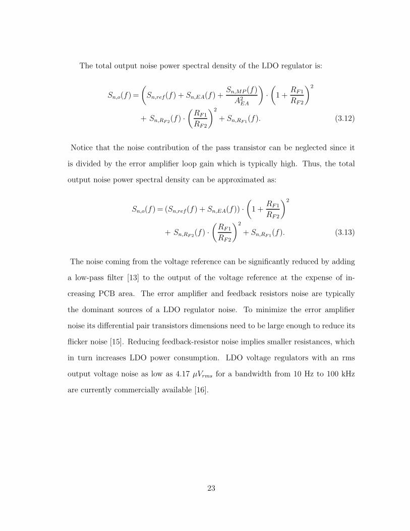
ABSTRACT
High-performance DC-DC voltage converters and high-efficient class-D audio am-
plifiers are required to extend battery life and reduce cost in portable electronics.
This dissertation focuses on new system architectures and design techniques to reduce
area and minimize quiescent power while achieving high performance. Experimental
results from prototype circuits to verify theory are shown.
Firstly, basics on low drop-out (LDO) voltage regulators are provided. Demand
for system-on-chip solutions has increased the interest in LDO voltage regulators that
do not require a bulky off-chip capacitor to achieve stability, also called capacitor-
less LDO (CL-LDO) regulators. Several architectures have been proposed; however,
comparing these reported architectures proves difficult, as each has a distinct pro-
cess technology and specifications. This dissertation compares CL-LDOs in a unified
manner. Five CL-LDO regulator topologies were designed, fabricated, and tested
under common design conditions.
Secondly, fundamentals on DC-DC buck converters are presented and area re-
duction techniques for the external output filter, power stage, and compensator are
proposed. A fully integrated buck converter using standard CMOS technology is
presented. The external output filter has been fully-integrated by increasing the
switching frequency up to 45 MHz. Moreover, a monolithic single-input dual-output
buck converter is proposed. This architecture implements only three switches instead
of the four switches used in conventional solutions, thus potentially reducing area in
the power stage through proper design of the power switches. Lastly, a monolithic
PWM voltage mode buck converter with compact Type-III compensation is pro-
posed. This compensation scheme employs a combination of Gm-RC and Active-RC
ii
techniques to reduce the area of the compensator, while maintaining low quiescent
power consumption and fast transient response. The proposed compensator reduces
area by more than 45% when compared to an equivalent conventional Type-III com-
pensator.
Finally, basics on class-D audio amplifiers are presented and a clock-free current-
controlled class-D audio amplifier using integral sliding mode control is proposed.
The proposed amplifier achieves up to 82 dB of power supply rejection ratio and a
total harmonic distortion plus noise as low as 0.02%. The IC prototype’s controller
consumes 30% less power than those featured in recently published works.
iii
DEDICATION
To my parents Aida and Miguel,
my aunt Irma, and my grandmother Maya
iv
ACKNOWLEDGEMENTS
I would like to express my sincere gratitude to my advisor, Dr. Edgar Sanchez-
Sinencio for his guidance, patience, and encouragement throughout the course of my
research. I would also like to thank Dr. Jose Silva-Martınez, Dr. Prasad Enjeti, and
Dr. Cesar Malave for serving on my committee.
I have had the pleasure of collaborating in research projects with: Miguel Rojas-
Gonzalez, Adrian Colli-Menchi, Mohamed El-Nozahi, Ahmed Amer, Seenu Gopal-
raju, Reza Abdullah, Xiaosen Liu, Chao Zhang, Jun Yan, and Hui Chen. Many
thanks to all of you. I also want to thank Ella Gallagher and Tammy Carda for their
invaluable assistance.
I would like to thank all my colleagues in the AMSC group; especially Salvador
Carreon, Fernando Lavalle, Jorge Zarate, Felix Fernandez, Raghavendra Kulkarni,
and Erik Pankratz for their friendship and valuable research discussions.
I am grateful to my best friend Luz for her comprehension and constant support
during these years. Finally, I want to express my deepest gratitude to my parents
Aida and Miguel, and my sisters Zobeida and Mirayda, for their unconditional love
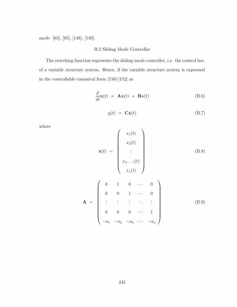
B.1 Model of a simple variable structure system. . . . . . . . . . . . . . . 241
B.2 Phase portraits of the second-order system in equation (B.1) for (a) Re-gion I when s(x1, x2, t) < 0 and (b) Region II when s(x1, x2, t) > 0. . 243
B.3 Phase portrait of the second-order system in equation (B.1) with slid-ing mode. . . . . . . . . . . . . . . . . . . . . . . . . . . . . . . . . . 244
Switched capacitor converters, also known as charge pumps, combine switches
and capacitors to generate a lower or higher DC output voltage than the DC input
voltage. They can also invert the voltage’s polarity. Typical peak efficiencies up to
90 % can be achieved in commercial switched-capacitor converters [5]-[6] for load
currents below 300 mA. On-chip switched capacitor voltage regulators can be used
8
to provide power to non-volatile memory circuits, dynamic random access memories
(DRAMs), and analog portions of mixed-signal circuits [2].
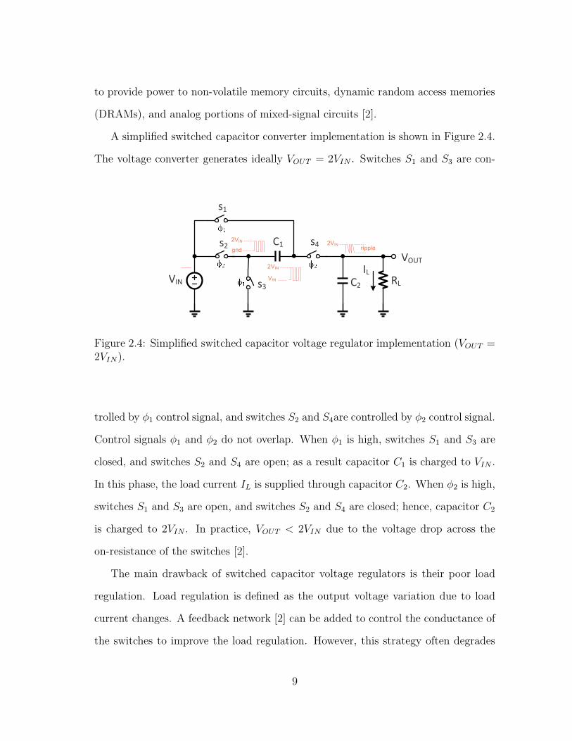
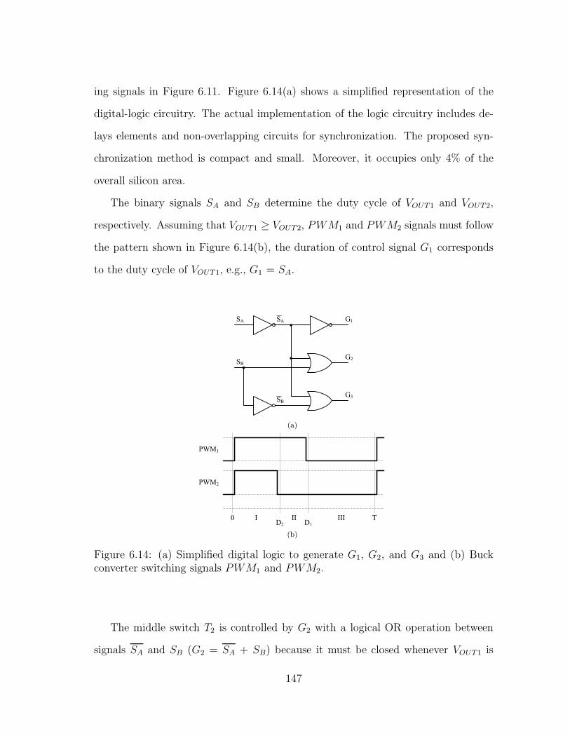
A simplified switched capacitor converter implementation is shown in Figure 2.4.
The voltage converter generates ideally VOUT = 2VIN . Switches S1 and S3 are con-
s1
s3
s2 s4C1
C2
VOUT
VIN RL
IL2VIN
VIN
2VIN
gnd2VIN
ripple
Figure 2.4: Simplified switched capacitor voltage regulator implementation (VOUT =2VIN).
trolled by φ1 control signal, and switches S2 and S4are controlled by φ2 control signal.
Control signals φ1 and φ2 do not overlap. When φ1 is high, switches S1 and S3 are
closed, and switches S2 and S4 are open; as a result capacitor C1 is charged to VIN .
In this phase, the load current IL is supplied through capacitor C2. When φ2 is high,
switches S1 and S3 are open, and switches S2 and S4 are closed; hence, capacitor C2
is charged to 2VIN . In practice, VOUT < 2VIN due to the voltage drop across the
on-resistance of the switches [2].
The main drawback of switched capacitor voltage regulators is their poor load
regulation. Load regulation is defined as the output voltage variation due to load
current changes. A feedback network [2] can be added to control the conductance of
the switches to improve the load regulation. However, this strategy often degrades
9
the efficiency due to the quiescent current required by the feedback circuit [2].
2.3.4 DC-DC Converters Comparison
Table 2.1 summarizes and compares the main characteristics of the three main
types of DC-DC converters. As can be seen, each topology has its own advantages
Table 2.1: DC-DC converters comparisonParameter Linear Switched-inductor Switched-capacitor
Efficiency Low High HighVoltage conversion Step down Step down/up Step down/up
Output voltage polarity Same Different DifferentArea Small Large Medium
Voltage regulation Good Good PoorNoise Low High High
Current Rating Low High Low
and disavantages. The selection of one topology over the other is application de-
pendent. Nevertheless, in portable applications the coexistence of both linear and
switching regulators is required since both accuracy and efficiency are necessary [7].
In these systems, a stable noise free voltage regulator is required to supply power
to noise sensitive circuits. A typical system is shown in Figure 2.5. A switching
VinSwitching
Regulator
Linear
Regulator
Vn Vout
Figure 2.5: Example of a power management system for portable applications.
converter steps down the input voltage to a lower voltage level but noisy (e.g., Vn).
10
Then a linear voltage regulator generates a low noise output voltage Vout from the
noisy voltage Vn. The purpose [7]-[8] of the switching is to step down the input
voltage in a more efficient way than the linear regulator; while the linear regulator’s
purpose is to filter the noise and generate a noise free supply voltage.
11
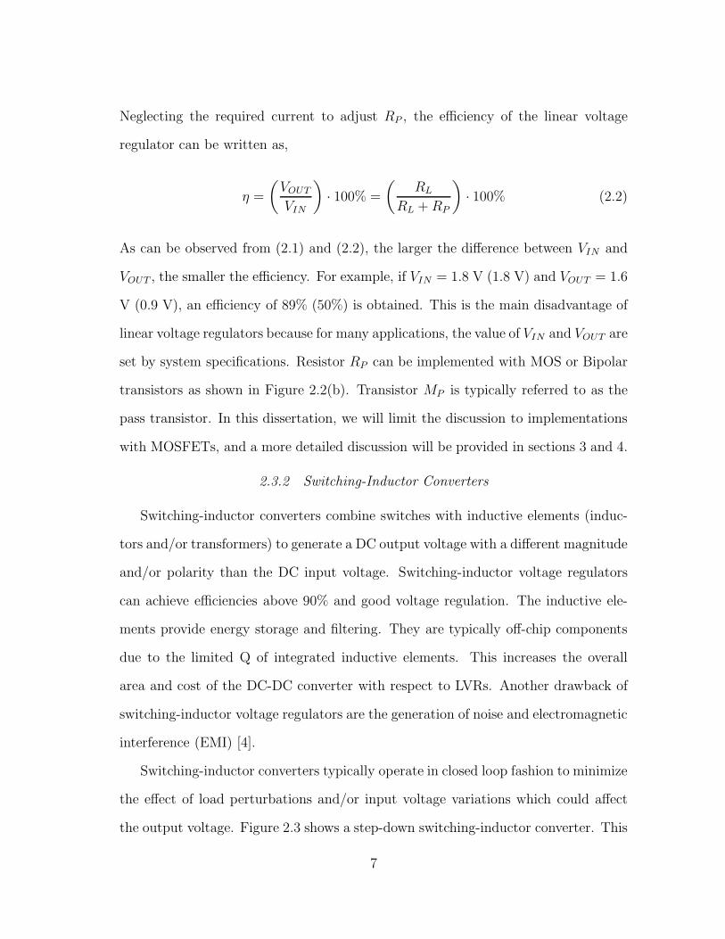
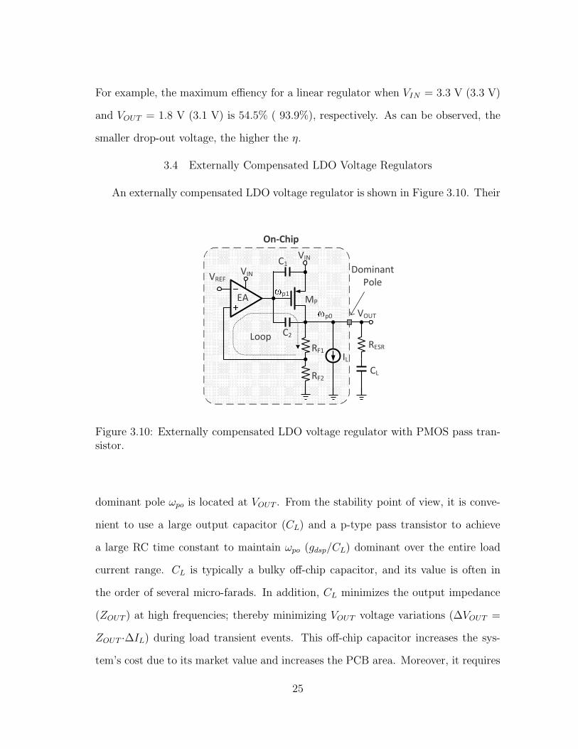
3. LOW DROP-OUT VOLTAGE REGULATORS ∗
3.1 Introduction
Low drop-out (LDO) voltage regulators are linear voltage regulators with a drop-
out voltage below 600 mV [7], typically in the value of 200 mV. LDO voltage regula-
tors can be classified into two main groups: externally and internally compensated.
Moreover, each group can be implemented with an N-type or P-type pass device.
This section discusses design specifications and different types of LDO voltage
regulators. In addition, guidelines for measuring voltage regulators and practical
design considerations are introduced. Finally, a simple design procedure for a LDO
voltage regulator is provided.
3.2 Basic Analysis
Before discussing the non-idealities of the LDO voltage regulator, ideal compo-
nents will be considered to introduce the basic concept. Figures 3.1 (a) and (b) show
the basic LDO architecture and small signal representation, respectively. Applying
Kirchhoff’s Current Law (KCL) at VOUT and VFB, the output voltage is found to be:
VOUT =gmpAEAVREF +
1+gmprdsprdsp
VIN
1rdsp
+ 1RL
+ 1RF1
− RF2
R1(RF1+RF2)+ RF2
RF1+RF2gmpAEA
(3.1)
where
β =RF2
RF2 +RF1
∗Part of this section is reprinted with permission from “Low Drop-Out Voltage Regulators:Capacitor-Less Architecture Comparison” by J. Torres et al., accepted for future publication inIEEE Circuits and Systems Magazine.
12
MP
LoopRF1
RF2
IL
VOUT
VREF
VIN
EA
VFBRF1
RF2
RL
rdsp
VOUT
gmp(VG-VIN)VIN
AEA(VFB-VREF)
VG
VFB
Load
(RL)
(a) (b)
Figure 3.1: (a) Basic LDO voltage regulator topology (b) small signal representation.
Assuming that the term βgmpAEA dominates over the other terms in the denominator
(this is typically the case in a well designed LDO voltage regulator) and 1 << gmprdsp,
(3.1) simplifies to:
VOUT∼= VREF
β+
VIN
βAEA(3.2)
Observe that VIN is attenuate by βAEA, and VREF is not. This shows that VOUT is a
scale version of VREF , and if βAEA is large enough, it has little dependency on VIN .
3.3 Design Specifications
Key design considerations for LDO voltage regulators include: stability, line/load
regulation, line/load transient, power supply rejection (PSR), noise, quiescent cur-
rent, drop-out voltage, and efficiency. Trade-offs for these parameters are often
topology dependent. Definitions for these performance parameters can be found in
Appendix A. A brief introduction to these design considerations is presented in this
section.
13
3.3.1 Stability
An LDO voltage regulator is a closed loop feedback system as shown in Figure 3.2.
It consists of an error amplifier (EA), pass transistor (MP ), feedback resistors (RF1,
RF2), and load capacitor CL. Capacitors C1 = Cgs + Cgb and C2 = Cgd, where
Cgb, Cgd, and Cgs are the pass transistor parasitic capacitances. Current source IL
represents the load. The stability of the system can be verified by breaking the loop
as shown in Figure 3.2 and obtaining the Bode plot. The LDO voltage regulator loop
must achieve positive phase margin at the unity gain frequency (UGF ) to be stable.
To achieve good transient response and minimize ringing, a phase margin greater
than 45 is often recommended. IL may vary several orders of magnitude (i.e., 100
µA to 50 mA) in LDO voltage regulators. This makes the LDO voltage regulator
stability analysis more complicated than in a typical amplifier.
MP
C2
C1
Loop
RF1
RF2
IL CL
VOUT
VREF
VIN
VIN
EA
Vfb1
Vfb2
p0
p1
Figure 3.2: LDO voltage regulator setup for stability analysis.
14
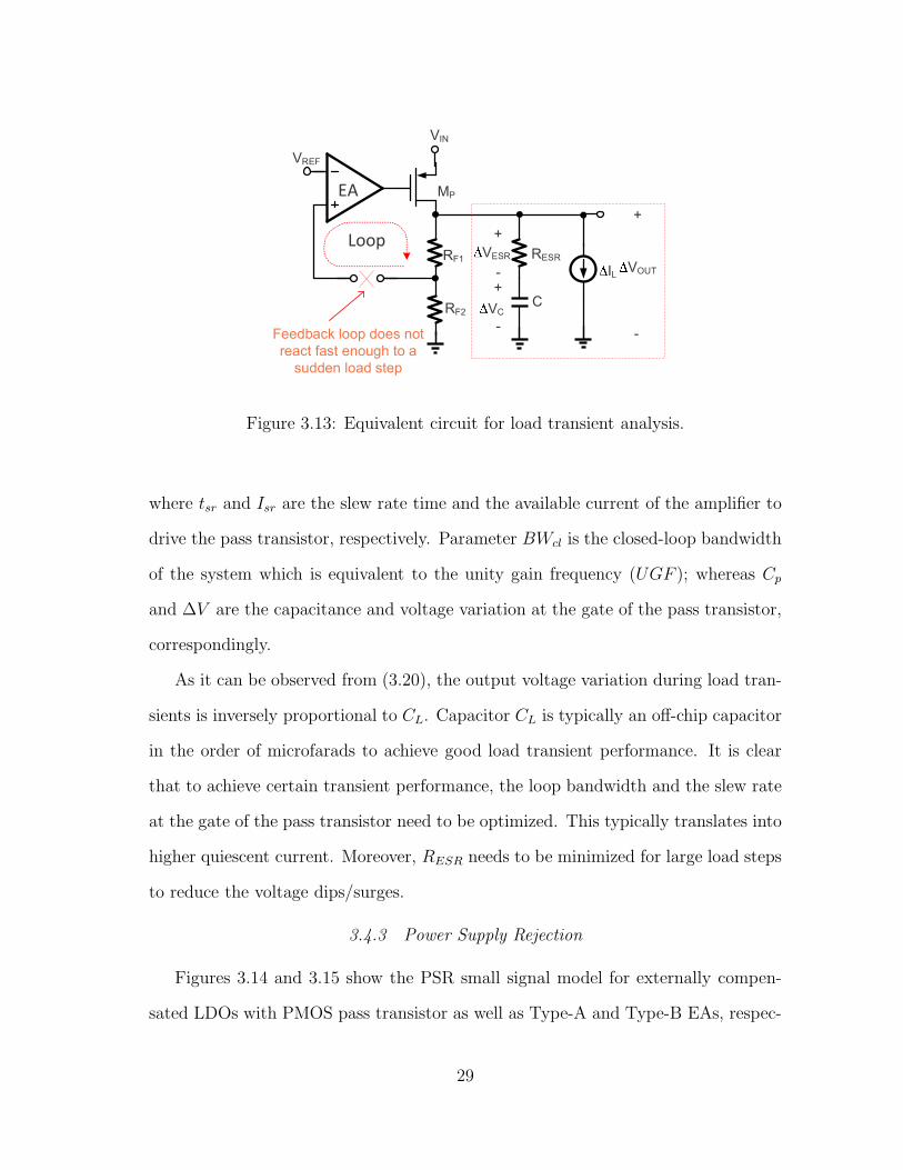
3.3.2 Load Transient
The load transient quantifies the peak output-voltage excursion and signal set-
tling time when the load current is stepped. An LDO regulator with good load-
transient response must achieve minimal overshoot/undershoot voltage and fast set-
tling time [9]. The load transient simulation setup is shown in Figure 3.3.
MP
C2
C1
Loop RF1
RF2
ILCL
VOUT
VREF
VIN
VIN
Zo
EArds
Figure 3.3: Load transient simulation setup.
3.3.3 Load Regulation
The load regulation also quantifies the voltage variation at the output when
change in the load current happens, but it is measured once the output voltage is in
steady state:
Load Regulation∆=
∆VOUT
∆IL
∣
∣
∣
∣
t→∞(3.3)
15
Hence, the load regulation is related to the closed loop DC output resistance of the
LDO Rout,cl (see Figure 3.3):
∆Vout = ∆IL · Rout,cl (3.4)
where
Rout,cl = Zo(s)|s=0 =Rout
1 + βgmpRoutAEA,o
∼= 1
βgmpAEA,o
. (3.5)
where gmp, β, and AEA,o represent the transconductance of the pass transistor, the
feedback factor RF2/(RF1 + RF2), and the EA DC gain, respectively. The open loop
resistance Rout is equal to the parallel combination of the pass transistor’s output
resistance (rdsp), load resistance (RL), and feedback resistors (RF1 +RF2). As seen
in (3.5), the higher AEA,o becomes, the smaller Rout,cl becomes resulting in better
load regulation. AEA,o at the maximum load current IL,max is particularly necessary
to achieve good load regulation. Parasitic resistances (e.g., due to PCB trace, bond-
ing wire, etc.) and systematic input-offset voltages can degrade the load regulation
performance even further [7]. Figure 3.4 shows a simplified block diagram of an LDO
voltage regulator including the equivalent PCB trace resistance (RTrace) and induc-
tance (LTrace), and equivalent bonding wire resistance (RB) and inductance (LB) [7].
The purpose of the Kelvin connection will be explained later in section 3.9.1.2.
3.3.4 Power Supply Rejection (PSR)
Before discussing in detail power supply rejection in LDO voltage regulators, the
difference between power supply rejection ratio (PSRR) in amplifiers and power
supply rejection (PSR) in LDO voltage regulators will be clarified since both terms
are often confused with each other. A general conceptual block diagram depicted in
Figure 3.5(a) shows the transfer functions from the power supply (VDD) and input
16
LDO Regulator IC
VOUT’
VSENSE
GND’
LB RB
LB RB
LB RB
LBRBPackage
LTrace RTrace
RESR
CL
GND
VOUT
RESR
CIN
LT
race
RT
race
Vs
VIN’
IL
Pin
VIN
Bondpad
Kelvin connection
Figure 3.4: Simplified block diagram of a LDO voltage regulators including PCBtrace and bonding wire parasitics.
(VIN) nodes to the output node (VOUT ) of an amplifier, and Figure 3.5(b) shows
a conceptual block diagram for the transfer function from the power supply node
(VDD) to the output node (VOUT ) of a LDO voltage regulator.
Power supply rejection ratio in amplifiers is define as:
PSRR(s) =A(s)
PSR(s)=
VOUT
VIN
VOUT
VDD
=VDD
VIN(3.6)
and PSR in linear voltage regulators is defined as:
PSR(s) =VOUT
VDD(3.7)
Hence, PSRR(s) and PSR(s) are related but they have different transfer functions
and as a result, they are different and should not be confused with each other.
PSR refers to the amount of voltage ripple at the output of the LDO coming
17
PSR(s)
A(s)
VDD
VIN
VOUT
(a)
Amplifier
PSR(s)VDD VOUT
LDO voltage regulator
(b)
Figure 3.5: General conceptual block diagrams for (a) an amplifier (b) LDO voltageregulator.
from the ripple at the input. The finite PSR in LDO regulators is due to several
paths between the input and output. Figure 3.6 shows four paths that could couple
input-voltage ripple to the LDO regulator output [10]. The ripple coming from
MP
C2
C1
Loop RF1
RF2
CL
VOUT
VREF
VIN
VIN
12
4
3
IL
rdsp
Figure 3.6: Input-to-output ripple paths in LDO regulators [10].
path 4 (voltage reference) is minimum when a high PSR voltage reference [10] is
implemented. Otherwise, it can be reduced by adding a low-pass filter to the output
18
of the voltage reference at the expense of increasing PCB area [11]. Therefore, the
ripple contribution due to path 4 is neglected. Regarding path 3, the PSR transfer
function of the LDO regulator strongly depends on the type of error amplifier [12]
and the type of device used as pass element. The concept of the Type-A and Type-B
error amplifiers was introduced in [12] to analyze the PSR of CL-LDO regulators.
It can be shown that the PSR of Type-A and Type-B EAs are approximately 1
or 0, respectively. Figures 3.7(a) and (b) show the Type-A small-signal model for
PSR analysis and an example of Type-A EA, respectively. Figures 3.8(a) and (b)
Ro2
Ro1Ro1
1/gm2
iVIN
i
VOUT-A
VIN
1/gm2 Ro2M2M2
Vin -VinM1 M1
IB
VOUT-A
(a) (b)
i
RB
Figure 3.7: (a) Small signal model for PSR of Type-A amplifiers and (b) transistorlevel example of Type-A amplifier [12].
show the Type-B small-signal model for PSR analysis and an example of Type-B
EA, respectively [12]. Current i is approximately VIN/Ro1 for Ro1 >> 1/gm2, where
Ro1∼= 1/gm1 + 2RB. Resistor RB represents the current source IB small signal
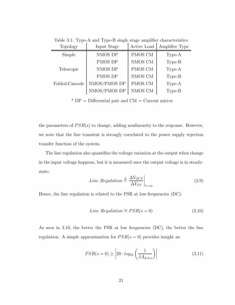
resistance. Table 3.1 classifies some common amplifier topologies in Type-A and
Type-B amplifiers. PSR analysis for externally and internally compensated LDO
voltage regulators is provided later in this section and will take into account Type-A
19
Ro1
Ro2
Ro1
1/gm2
iVIN
i
VOUT-B
VIN
1/gm2
M1 M1
Vin -Vin
M2M2 Ro2
IB
(a) (b)
VOUT-B
RB
i
Figure 3.8: (a) Small signal model for PSR of Type-B amplifiers and (b) an exampleof Type-B error amplifier [12].
and Type-B amplifiers.
3.3.5 Line Transient and Regulation
Line transient measures the output voltage variation in response to a voltage
step at the input of the LDO regulator. Line transient is related to PSR, since both
quantify the change in VOUT due to a variation in VIN ; however, they differ in that
line transient/PSR are large/small-signal parameters, respectively [11]. Nevertheless,
improving PSR at low and high frequencies typically improves line regulation and
line transient response, respectively. Assuming, for the sake of simplicity, that we
can apply small-signal perturbation analysis, then
∆VOUT = PSR(s) ·∆VIN (3.8)
where ∆ VIN = Vstep/s in the Laplace domain and PSR(s) is the power supply
rejection transfer function of the system. In fact, small changes in VIN would cause
20
Table 3.1: Type-A and Type-B single stage amplifier characteristics
Topology Input Stage Active Load Amplifier Type
Simple NMOS DP PMOS CM Type-A
PMOS DP NMOS CM Type-B
Telescopic NMOS DP PMOS CM Type-A
PMOS DP NMOS CM Type-B
Folded-Cascode NMOS/PMOS DP PMOS CM Type-A
NMOS/PMOS DP NMOS CM Type-B
* DP = Differential pair and CM = Current mirror.
the parameters of PSR(s) to change, adding nonlinearity to the response. However,
we note that the line transient is strongly correlated to the power supply rejection
transfer function of the system.
The line regulation also quantifies the voltage variation at the output when change
in the input voltage happens, but it is measured once the output voltage is in steady-
state:
Line Regulation∆=
∆VOUT
∆VIN
∣
∣
∣
∣
t→∞(3.9)
Hence, the line regulation is related to the PSR at low-frequencies (DC):
Line Regulation ∼= PSR(s = 0) (3.10)
As seen in 3.10, the better the PSR at low frequencies (DC), the better the line
regulation. A simple approximation for PSR(s = 0) provides insight as:
PSR(s = 0) ≥∣
∣
∣
∣
20 · log10(
1
βAEA,o
)∣
∣
∣
∣
(3.11)
21
3.3.6 Noise
Noise in LDO regulators refers to the thermal and flicker noise in transistors
and resistors. It can be specified as output voltage noise spectral density (V/√Hz)
or as integrated output noise voltage (Vrms), which is essentially the output spec-
tral noise density integrated over a bandwidth [13]-[14]. For instance, if the LDO
provides a regulated voltage to a voltage-control oscillator (VCO), the output spec-
tral noise density curve would prove more useful for phase-noise/jitter computation.
If instead, the LDO regulated an ADC, then the integrated RMS noise could be
more appropiate [14]. Fig. 3.9 shows the main noise contributors in an LDO reg-
Medium-to-high Dominated by CL, minimum value Determine by the loop tranfer function
frequencies is limited by RESR
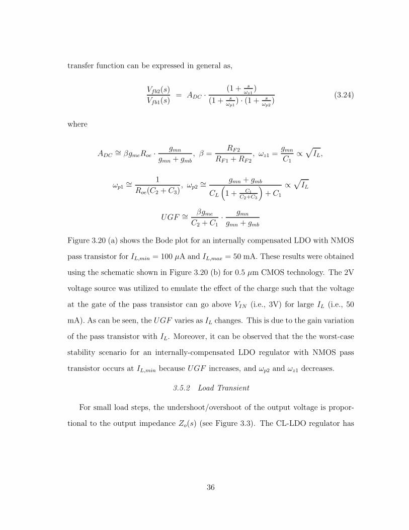
For large load current steps, the analysis is particularly challenging since the pass
transistor operates in three different operating regions (E.g. subthreshold, saturation,
38
and triode regions) over the entire load current range. In addition, the transconduc-
tance, conductance, and parasitic capacitors of the pass transistor vary dynamically
with the load current, thereby complicating the analysis even further. Figure 3.21
shows an illustrative example of how the CL-LDO output impedance varies as the
load current changes and how the pass transistor operates in different regions over
the entire load current range. Figure 3.22 depicts the parasitic capacitance of the
10-1
100
101
0
50
100
150
200
Load Current (mA)
Ou
tpu
t Im
pe
da
nce
at
DC
(m
Ω)
saturation region
tri
od
e r
eg
ion
subthreshold region
Figure 3.21: Output impedance at DC versus load current.
pass transistor variation versus load current. As can be seen, the CL-LDO output
impedance and the parasitic capacitances of the pass transistor significantly vary
over the entire current range. Fortunately, it has been observed that improving the
slew rate (a large signal parameter) helps to minimize the undershoots/overshoots
during large load current steps. In CL-LDO regulators, the slew rate (Ibias/Cgate) is
highly dependent on total capacitance at the gate of the pass transistor and the bias
current of the EA’s stage driving it. Figure 3.23 shows an example of how the Vout
undershoot amplitude varies versus the bias current of the EA’s output stage. As
39
10-1
100
101
0
10
20
30
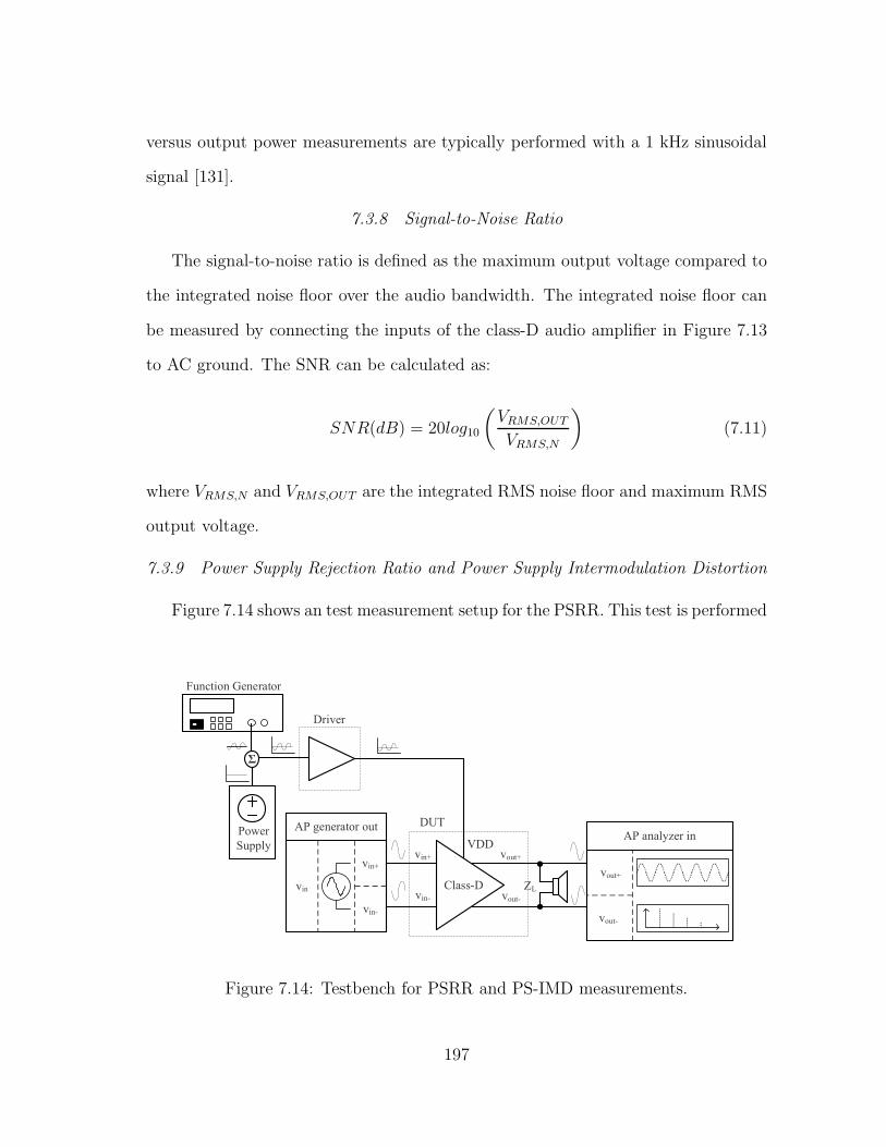
40
50
60
Load Current (mA)
Ca
pa
cita
nce
(p
F)
Cgs
Cgd
Cgb
saturation region
trio
de
re
gio
n
subthreshold region
Figure 3.22: MP parasitic capacitance versus load current.
0
5
10
15
Bias current
Re
du
ctio
n i
n V
ou
t u
nd
ers
ho
ot
am
pli
tud
e (
%)
IB
10IB
Figure 3.23: Reduction in output voltage undershoot amplitude versus bias current.
can be seen, the undershoot amplitude reduces as the bias current increases. In Sec-
tion 4, several architectures that emphasize on improving the slew rate in CL-LDO
voltage regulators will be discussed. The main idea behind all of them is increasing
the charging/discharging current at the gate of the pass transistor during large load
transient events.
40
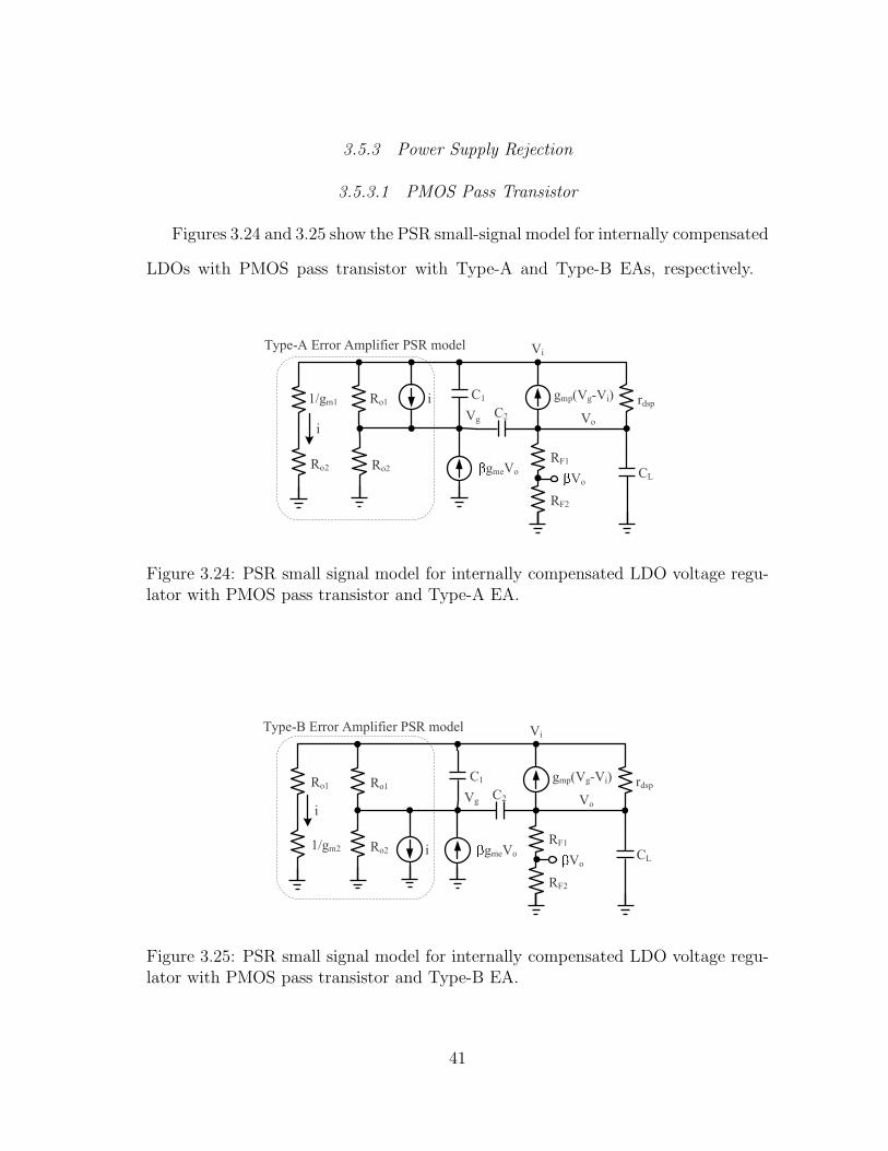
3.5.3 Power Supply Rejection
3.5.3.1 PMOS Pass Transistor
Figures 3.24 and 3.25 show the PSR small-signal model for internally compensated
LDOs with PMOS pass transistor with Type-A and Type-B EAs, respectively.
Ro1
Ro2Ro2
1/gm1
i
i
Vg
Vi
Vo
gmeVo
C1
C2
RF2
RF1
gmp(Vg-Vi) rdsp
CL
Type-A Error Amplifier PSR model
Vo
Figure 3.24: PSR small signal model for internally compensated LDO voltage regu-lator with PMOS pass transistor and Type-A EA.
Ro1
Ro2
Ro1
1/gm2
i
i
Vg
Vi
Vo
gmeVo
C1
C2
RF2
RF1
gmp(Vg-Vi) rdsp
CL
Type-B Error Amplifier PSR model
Vo
Figure 3.25: PSR small signal model for internally compensated LDO voltage regu-lator with PMOS pass transistor and Type-B EA.
41
These small-signal models are based on Figure 3.16(a).
The PSR transfer function can be approximated as,
Vo(s)
Vi(s)= PSRDC ·
(1 + sωz1,psr
) · (1 + sωz2,psr
)
(1 + sωp1,psr
) · (1 + sωp2,psr
)(3.27)
where
PSRDC∼= 1 + gmprdsp(1− APSR)
βgmprrdspgmeRoe
, ωz2,psr =gmp
C1
,
ωp1,psr =βgme
C2, ωp2,psr =
gmp
CL
(
1 + C1
C2
)
+ C1
Table 3.4 shows the analytical expressions for ωz1,psr and |PSR|DC for an internally
compensated LDO voltage regulator implemented with Type-A and Type-B error
amplifiers. As can be seen from Table 3.4, the LDO voltage regulator implemented
with a Type-A amplifier presents higher DC PSR than the one implemented with a
Type-B amplifier for the same loop gain.
Table 3.4: Analytical expressions for PSR of an internally compensated LDO voltageregulator with PMOS Pass Transistor
Error Amplifier APSR ωZ1,psr |PSR|DC
Type− A 1 1/(gmprdspC2Roe)1
βgmeRoegmprdsp
Type− B 0 1/(RoeC2)1
βgmeRoe
3.5.3.2 NMOS Pass Transistor
Figures 3.26 and 3.27 show the PSR small signal model for internally compensated
LDOs with NMOS pass transistor with Type-A and Type-B EAs, respectively. These
small signal models are based on Figure 3.16(b). The PSR transfer function can be
42
approximated as,
Ro1
Ro2Ro2
1/gm1
i
i
Vg
Vi
Vo
gmeVo
C1
C2
RF2
RF1
gmn(Vg-Vo) rdsn
CL
Type-A Error Amplifier PSR model
Vo
C3
gmbVo
Figure 3.26: PSR small-signal model for externally compensated LDO voltage regu-lator with NMOS pass transistor and Type-A EA.
Ro1
Ro2
Ro1
1/gm2
i
i
Vg
Vi
Vo
gmeVo
C1
C2
RF2
RF1
gmn(Vg-Vo) rdsn
CL
Type-B Error Amplifier PSR model
Vo
C3
gmbVo
Figure 3.27: PSR small-signal model for internally compensated LDO voltage regu-lator with NMOS pass transistor and Type-B EA.
Vo(s)
Vi(s)= PSRDC ·
(1 + sωz1,psr
) · (1 + sωz2,psr
)
(1 + sωp1,psr
) · (1 + sωp2,psr
)(3.28)
where
PSRDC∼= 1 + gmnrdspAPSR
βgmnrrdspgmeRoe, ωz2,psr =
gmn
C1,
43
ωp1,psr =βgme
C2 + C3, ωp2,psr =
gmn
CL
(
1 + C1
C2+C3
)
+ C1
Table 3.5 shows the analytical expressions for ωz1,psr and |PSR|DC for an internally
compensated LDO voltage regulator implemented with NMOS pass transistor for
Type-A and Type-B error amplifiers. As can be seen from Table 3.5, the LDO
voltage regulator implemented with a Type-B amplifier presents higher DC PSR
than the one implemented with a Type-A amplifier for the same loop gain.
Table 3.5: Analytical expressions for PSR of an internally compensated LDO voltageregulator with NMOS Pass Transistor
Error Amplifier APSR ωZ1,psr |PSR|DC
Type−A 1 1/(C2Roe)1
βgmeRoe
Type− B 0 1/(gmnrdsnRoeC2)1
βgmeRoegmnrdsn
3.5.4 PMOS Versus NMOS Pass Transistor
Table 3.6 compares CL-LDO voltage regulators implemented with NMOS and
PMOS pass transistors. As can be observed in Table 3.6, CL-LDO voltage regula-
tors implemented with PMOS pass transistors have smaller drop-out voltage than
the ones implemented with NMOS. This make PMOS implementations more power
efficient than NMOS implementations. Moreover, PMOS implementations operate
with smaller input voltages than NMOS implementations for the same output volt-
age. The maximum current in NMOS implementations is smaller than PMOS im-
plementations due to the limited voltage swing at the gate of the pass transistor.
The drop-out voltage in a CL-LDO voltage regulator with NMOS pass transistor
can be reduced if a charge pump is used to power the EA [19] or the pass transistor
44
is implemented with a natural Vth NMOS device.
Table 3.6: PMOS versus NMOS pass transistor comparison
Parameter NMOS PMOS
Drop-out voltage (VDO) VSD(sat) + Vth VSD(sat)
VIN,min Vo + VDO Vo + VDO
Output Resistance 1gm
rds
Io,max Low Moderate
Efficiency Moderate High
Transient Response Fast Moderate
PSR Good Moderate
NMOS implementations usually have better transient response than PMOS due
to their small open loop output resistance. In addition, implementations with NMOS
pass transistor offers better PSR performance for the same loop gain as shown in Fig-
ure 3.28. This is due to the fact that having the same loop gain implicates that gmeRoe
102
103
104
105
106
107
-60
-50
-40
-30
-20
-10
0
Frequency (Hz)
Po
we
r S
up
ply
Re
ject
ion
(d
B)
NMOS PT, Type-A EA
PMOS PT, Type-A EA
NMOS PT, Type-B EA
PMOS PT, Type-B EA
Figure 3.28: Internally compensated LDO voltage regulator PSR.
45
in (3.24) is greater than in (3.23) and hence, βgmnrdsngmeRoe > βgmprdspgmeRoe.
Moreover, the combination of the PMOS pass transistor with the load acts as a
common gate amplifier from VIN to VOUT , while the combination of the NMOS pass
transistor with the load acts as a voltage divider from VIN to VOUT ; as a result, the
implementation with NMOS provides more isolation between the VIN and VOUT at
high frequencies. This translates into better PSR performance at high frequencies
for the implementation with a NMOS pass transistor.
3.6 Externally Versus Internally Compensated LDO Voltage Regulators
Table 3.7 qualitatively compares externally and internally compensated LDO
voltage regulators [7]. As can be seen, externally compensated LDO voltage regula-
Table 3.7: Externally versus internally compensated LDO voltage regulators com-parison
Externally Compensated Internally Compensated
Application Higher Power Lower Power
(E.g. heavier loads) (E.g. lighter loads)
Load Capacitor CL Off-chip or in-package On-chip or in-package
Load Transient Better Worse
(E.g. smaller ∆ VOUT ∝ 1/CL) (E.g. larger ∆VOUT )
Worst Case Stability Large IL Small IL
PSR Better Worse
(E.g. higher ωp1) (E.g. lower ωp1)
Cost Higher Lower
tors exhibit in general better performance than internally compensated ones at the
expense of higher cost. The off-chip capacitor CL provides low output impedance in
externally compensated LDO voltage regulators. This reduces the voltage dips/surges
46
during load transient events when compared with internally compensated LDO volt-
age regulators. For the same reason, externally compensated LDO voltage regulators
can deal with heavier loads than internally compensated ones.
3.7 Guidelines for Measuring LDO Voltage Regulators
LDO voltage regulator measurements include: efficiency, load regulation/transient,
line regulation/transient, and PSR. Basic voltage regulator characterization requires
the following measurement equipment: power supplies, multi-meters, an oscilloscope,
waveform generators, power resistors, and an evaluation board.
3.7.1 Efficiency Measurement Setup
The power efficiency of a voltage regulator is given by:
η =POUT
PIN
=ILVOUT
IINVIN
≤ ILVOUT
IIN (VOUT + VDO)(3.29)
where IL represents the load current and VOUT represents the output voltage. Pa-
rameters VIN and IIN represent the input voltage and current of the LDO voltage
regulator, respectively. Hence, efficiency can be calculated by measuring IL, VOUT ,
IIN , and VIN with a multi-meter.
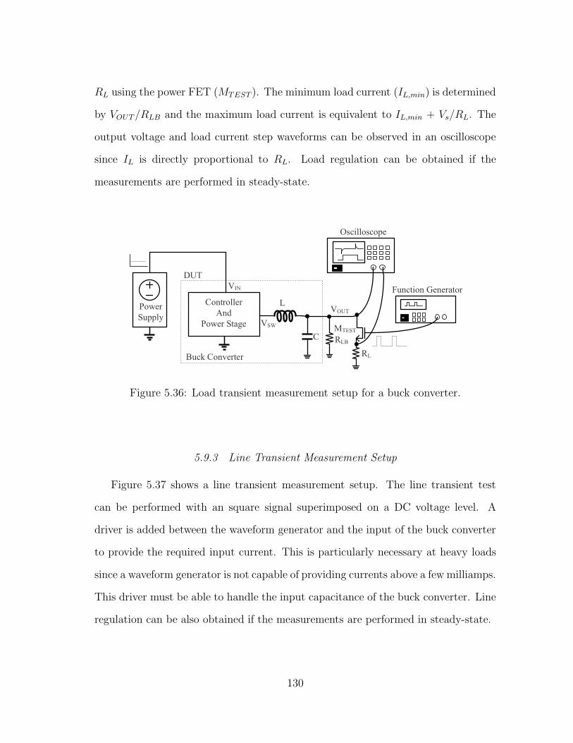
3.7.2 Load Transient Measurement Setup
Figure 3.29 shows a load transient measurement setup. The load step is generated
by switching the connection between the output voltage VOUT and the load resistance
RL using the power FET MTEST . The minimum load current (IL,min) is determined
by VOUT/RLB and the maximum load current is equivalent to IL,min + Vs/RL. The
output voltage and load current step waveforms can be observed in an oscilloscope
since IL is directly proportional to RL. Load regulation can be obtained if the
measurements are performed in steady state.
47
Oscilloscope
Voltage
Regulator
VINDUT
Power
Supply
Function Generator
RL
MTEST
RLB
VOUT
Vs
Figure 3.29: Load transient measurement setup.
3.7.3 Line Transient Measurement Setup
Figure 3.30 shows a line transient measurement setup. The line transient test
can be performed with a square signal superimposed on a DC voltage level. A driver
is added between the waveform generator and the input of the voltage regulator to
provide the required input current. This is particularly necessary at heavy loads since
a waveform generator is not capable of providing currents above a few milliamps. In
addition, this driver needs to be able to handle the input capacitance of the LDO
voltage regulator. Line regulation can also be obtained if the measurements are
performed in steady state.
3.7.4 PSR Measurement Setup
The measurement setup for line transient (Figure 3.30) can be used for PSR. The
only difference is that a sinusoidal signal instead of a square signal is imposed on a
DC voltage level. The peak-to-peak amplitude of the sinusoidal signal is typically in
the order of 20-100 mV [7]. The PSR is the ratio between VOUT and VIN and can be
obtained using an oscilloscope. Due to the amplitude of the sinusoidal signal, PSR
48
Oscilloscope
Function Generator
Voltage
Regulator
Driver
VINDUT
Σ
Power
Supply
RL
VOUT
Figure 3.30: Line transient measurement setup.
simulation results based on AC analysis may not correlate with measurement results.
Hence, PSR simulation results based on transient simulations may correlated better
with experimental results since the test bench is closer to the actual one used in
measurements [7].
3.8 Design Strategy in LDO voltage regulators
Figure 3.31 shows a design flow for LDO voltage regulators. It begins with the ba-
sic DC requirements VIN , VOUT , IL, and IQ specifications. From these specifications,
the dimensions of the pass transistor can be chosen:
W
L=
2IL
Kp (VDS,sat)2 =
2IL
Kp (VDO)2 (3.30)
Minimum length is typically chosen to minimize the gate capacitance of the pass
transistor which affects the stability, transient response, and PSR performance. The
feedback resistors can be chosen from the ratio between the VOUT and VREF and IQ
specifications:
VOUT = VREF ·(
1 +RF1
RF2
)
(3.31)
49
VOUT VIN
VDO IL
Pass Transistor
Dimensions (W/L)
Design
Error Amplifer
Cgb rdsCgsCgd gme Roe Cp
Calculate poles and zeros
Externally Compensated:
Set dominant pole with CL and adjust
compensation zero with RESR
Internally Compensated:
If necessary add compensation
capacitor Cm to set dominant pole
Check Stability over the
entire load current range
Check load/line transient, load/line
regulation, PSR, noise, quiescent current,
efficiency, etc.
Feedback Resistors
(RF1/RF2)
Basic DC specifications
VREF
IQ
Figure 3.31: Low dropout voltage regulator design flow.
H · IQ =VOUT
RF1 +RF2(3.32)
where H·IQ is a percentage of the total quiescent current budget. The feedback
resistors can be found using (3.31) and (3.32). The poles and zeros can be estimated
from the pass transistor dimensions, feedback resistors, and error amplifier small
signal parameters. Then, on an externally compensated LDO, the CL capacitor can
be chosen to set the dominant pole and RESR to place the compensation zero at
50
the desired location for stability purposes. In the case of an internally compensated
LDO, a compensation capacitor can be used to set the dominant pole. The loop’s
stability can be verified by following the proposed procedure. After verifying stability,
performance paramters (e.g., load/line regulation, PSR) can be simulated to check if
specifications are met. Otherwise, the pass transistor dimensions, feedback resistors
values and/or EA design (e.g., bias current, compensation capacitance, transistor
dimensions, etc.) can be modified.
In summary, the LDO voltage regulator design starts with the pass transistor or
feedback resistors, and then EA. Next, specifications are verified, and if necessary,
the pass transistor, feedback resistors, and EA can be modified to meet requirements.
3.9 Practical Design Considerations for LDO Voltage Regulators
3.9.1 Pass Transistor
3.9.1.1 Design
As explained previously in this section, the pass transistor design affects the effi-
ciency, PSR, transient, minimum input voltage, and maximum delivered load current
(see Table 3.6). The noise contribution of the pass transistor is typically neglectable
when compared with the first stage of the EA and feedback resistors contribution.
Moreover, the dimensions of the pass transistor can be calculated based on VIN ,
VOUT , and IL as shown in (3.30). For a PMOS pass transistor assuming operation in
the saturation region, the dimensions can be calculated using the following equation:
(
W
L
)
PMOS
=2IL,max
Kp (VDS,sat)2 =
2IL,max
Kp (VDO)2 (3.33)
51
and for an NMOS pass transistor, the dimensions can be obtained with:
(
W
L
)
NMOS
=2IL,max
Kn (VDS,sat)2 =
2IL,max
Kn (VDO)2 (3.34)
Notice that in (3.34), it is assumed that voltage at the gate of the pass transistor
could go above VIN to provide the necessary maximum load current. This can be
achieved using a charge pump to bias the error amplifier. For the same VDS,sat, the
dimensions of the pass transistor implemented with NMOS and PMOS are related
by:(
W
L
)
PMOS
=Kn
Kp
(
W
L
)
NMOS
(3.35)
Typically, Kn ≥ 3Kp and as a result, a P-Type pass transistor generally occupies a
larger area than the N-Type. However, for a fair comparison the area occupied by
the charge pump (e.g., capacitors) needs to be included.
Due to the large IL range in most LDO voltage regulators, the pass transistor may
operate over three different regions (e.g., subthreshold, saturation, triode regions).
This complicates the modeling of the pass transistor since an IL dependent model
is required to represent the pass transistor’s parameters (e.g., gm, gds, cgs) over the
entire IL range (see Figures 3.21 and 3.22 for details). Therefore, two possibilities
to model the pass transistor are: a) using a piece-wise approximation where the
switching points are defined by the operating region and each parameter is defined
according to its respective equation for each operating region or b) using a general
polynomial expression as:
P (IL) = p0 + p1IL + p2I2L + ..... + pnI
nL (3.36)
where pi (for i = 0, 1, 2,..., n) are the coefficients for a fitted polynomial for each
52
parameter in terms of IL.
3.9.1.2 Layout
The track resistance (resistance between drain/source and bondpad), bond-wire
resistance (resistance between bondpad and pin), and printed board circuit trace
resistance affect the effective drop-out voltage [7]. To minimize the track resistance,
use as many contacts and wide tracks for the drain and source terminals to mini-
mize sheet and via resistances. This is critical since these terminals carry the load
current. Also, the pass transistor should be placed as close as possible to the bond-
pad to minimize track resistance [7]. Top metals should be used for power routing
since they have the smallest resistance. In addition, multiple metals in parallel can
be used to minimize the track resistance. To reduce the bond-wire resistance and
inductance, multiple parallel bond-wires can be used for the drain and source termi-
nals. To minimize the effect of the bond-wire resistance in the load regulation, the
output voltage is sensed at the pin instead of the drain/source of the PMOS/NMOS
pass transistor. By doing this, the bond-wire resistance is included in the feedback
loop and as a result, better load regulation is achieved. This technique requires an
additional bondpad and bond-wire. The output of the pass transistor is connected
to VOUT pin through V ′OUT bondpad and a bondwire; and the feedback resistors are
connected to VOUT pin through VSENSE bondpad and another bondwire as shown in
Figure 3.4. This technique is known as the Kelvin or Star connection [7].
3.9.2 Error Amplifier
3.9.2.1 Design
The accuracy and quiescent power consumption of the LDO voltage regulator are
highly dependent on the EA design. As already explained in this section, line/load
regulation and DC PSR are inversely proportional to the DC gain of the EA. More-
53
over, the DC PSR also depends on the Type of EA (e.g., Type-A or Type-B). The
EA’s bandwidth affects the load/line transient performance of the LDO voltage reg-
ulator. Typically, a multi-stage EA is implemented to deal with the gain and band-
width challenges. The first stage usually provides most of the DC gain and the last
stage typically consumes most of the quiescent current to place the non-dominant
pole beyond UGF and improve the slew rate at the gate of the pass transistor. The
differential pair of the EA should be sized carefully to minimize the flicker noise with-
out increasing too much the input capacitance of the EA. If the input capacitance
is large enough, it can generate an undesirable pole that affects the loop’s stability.
In battery-powered applications, the EA must be designed to meet all the specifica-
tions with the smallest amount of quiescent current to extend the battery life. The
systematic and random offsets of the EA should be minimized since it can affect the
regulation of the system. In addition, the EA should be able to operate properly
for the input voltage range, voltage reference voltage, and load current range which
modifies the output voltage swing of the EA. Hence, an EA with high DC gain, high
bandwidth, low IQ, low noise, and low input offset is desired [7].
3.9.2.2 Layout
The error amplifier should be laid out using standard layout techniques such
as common centroid and interdigitized configurations and use dummy components
for best matching [20]. The differential pair and active current load require critical
matching to minimize offset as well as placing as many substrate contacts as possible
in local cells to provide homogeneous bulk voltage for the transistors. This minimizes
threshold voltage variation among them. Using P+ guard ring and N+ guard ring
for NMOS and PMOS transistors, respectively [21]. Figure 3.32 shows an example
of an error amplifier transistor level implementation and layout with the suggestions
54
previously mentioned.
D1 D1 D1D2 D2S S S S
D3 D3 D3D4 D4S S S S
VIN-
VIN+
S5 S5 S5D5 D5
VB
VOUT
VOUT
VIN-VIN+
VB
4xM14xM2
4xM3 4xM4
4xM5
S S
S S
(a) (b)
Dummies
Nwell
Poly
N+ guard ring
P+ guard ring
Dummies
Dummies
Metal 2
Metal 1
Active
Figure 3.32: Example of an error amplifier (a) transistor level (b) layout implemen-tation.
3.9.3 Printed Board Circuit
3.9.3.1 Design
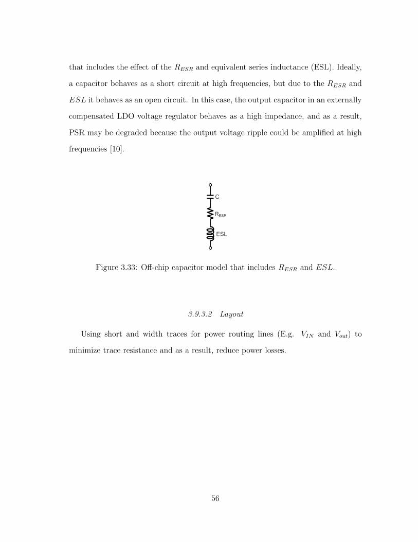
Using ceramic capacitors with low ESR at the output to minimize voltage dip/surge
amplitudes (ILRESR) during load transient events. Multiple capacitors can be used
in parallel to increase the capacitance and reduce RESR to improve even further the
load transient response. It is advised to place a capacitor from the input of the LDO
voltage regulator to ground to reduce the input voltage ripple and spikes before they
reach the LDO voltage regulator [22]. In addition, it is also advised to include the
capacitor model in simulations. Figure 3.33 shows a model for an off-chip capacitor
55
that includes the effect of the RESR and equivalent series inductance (ESL). Ideally,
a capacitor behaves as a short circuit at high frequencies, but due to the RESR and
ESL it behaves as an open circuit. In this case, the output capacitor in an externally
compensated LDO voltage regulator behaves as a high impedance, and as a result,
PSR may be degraded because the output voltage ripple could be amplified at high
frequencies [10].
C
RESR
ESL
Figure 3.33: Off-chip capacitor model that includes RESR and ESL.
3.9.3.2 Layout
Using short and width traces for power routing lines (E.g. VIN and Vout) to
minimize trace resistance and as a result, reduce power losses.
56
4. LOW DROP-OUT VOLTAGE REGULATORS: CAPACITOR-LESS
ARCHITECTURE COMPARISON∗
4.1 Introduction
Demand for system-on-chip solutions has increased the interest in LDO voltage
regulators which do not require a bulky off-chip capacitor to achieve stability, also
called capacitor-less LDO (CL-LDO). Several architectures have been proposed; how-
ever comparing these reported architectures proves difficult, as each has a distinct
process technology and specifications. This chapter compares CL-LDOs in a unified
matter. We designed, fabricated, and measured five illustrative CL-LDO regulator
topologies [18], [23]-[26] in the same process (0.5µm CMOS) under common design
specifications to facilitate comparison. We compare the architectures in terms of
(1) line/load regulation, (2) power supply rejection, (3) line/load transient, (4) total
on-chip compensation capacitance, (5) noise, and (6) quiescent power consumption.
Our remarks and observations are suitable for the chosen design constraints.
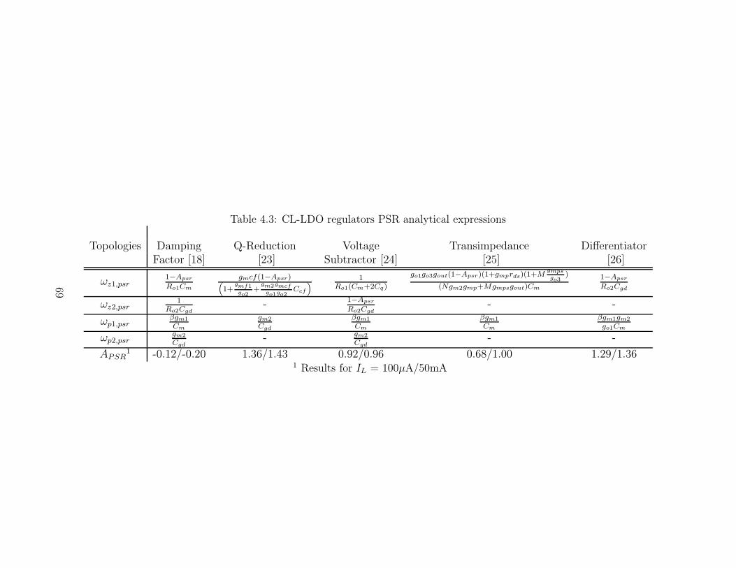
This chapter presents representative CL-LDO regulator topologies [18], [23]-[26]
and [27]-[44]. In addition, remarks on CL-LDO regulator architectures and experi-
mental results are provided. Finally, conclusions are drawn.
4.2 Comparison of CL-LDO Regulator Topologies
We categorize several illustrative CL-LDO regulator topologies into 3 groups. In
this section, it is assumed that the gain stages are powered from VIN unless otherwise
specified.
∗This section is reprinted with permission from “Low Drop-Out Voltage Regulators: Capacitor-LessArchitecture Comparison” by J. Torres et al., accepted for future publication in IEEE Circuits andSystems Magazine.
57
4.2.1 Advanced Compensation Topologies
Topologies [18] and [23] are two of the first CL-LDO regulators. They are based
on Miller pole splitting compensation to achieve small on-chip compensation capac-
itance when compared with the conventional (externally compensated) LDO regula-
tor. In Figure 4.1 (a) [18], a damping-factor circuit stabilizes the LDO regulator for
various capacitive load conditions. The LDO regulator requires the damping factor
compensation (DFC) circuit to be stable with and without an off-chip capacitor. In
a capacitor-less configuration, the damping factor circuitry might not be necessary
since the feedback loop is effectively compensated with the Miller-compensation ca-
pacitor Cm. The dominant pole is given by A2ApCm and the output resistance of
the EA first stage A1. Ap is the gain of the pass transistor. In this chapter, we will
refer to this topology as the Damping Factor architecture. Figure 4.1(b) shows
VIN
A1
-
+
VREF
MP
RF1
RF2
(a)
No CL-LDO
Configuration
A2
VOUTCm
-ADF
CDF
VIN
A1
-
+
VREF
MP
RF1
RF2
(b)
A3
VOUTCm
-AF
CQ
A2
Figure 4.1: CL-LDOs with improved frequency compensation techniques (a) DFC[18], (b) Q-Reduction [23].
the Q-reduction architecture. This architecture was proposed to minimize on-chip
58
capacitance and quiescent current [23]. The Q-reduction circuit is formed by CQ
and the transconductance A2. The Q-reduction technique controls the Q of the
non-dominant complex poles to improve the stability at light loads.
4.2.2 Load Transient Topologies
Approaches that improve the load transient comprise either pass-transistor-gate-
voltage slew-rate enhancement with multiple active loops [25]-[34] and/or output-
impedance reduction [35]-[39].
Architecture in [26] and [27] employ a current amplifier Ai in series with capaci-
tance Cf that acts as an auxiliary fast loop in addition to the main voltage loop as
shown in Figure 4.2 (a). The capacitance Cf reacts to sudden changes on VOUT dur-
ing load transients by generating an equivalent transient current (if). Then, current
if is amplified by the gain Ai and injected into the pass transistor’s gate capaci-
tance. Thus, this auxiliary loop improves the transient response. Moreover, it helps
to achieve internal compensation since the dominant pole of the system is defined by
ωd∼= 1/(AiApCf Roi‖Ro1) where Roi and Ro1 are the output resistances of Ai and A1,
respectively. [28] expands on this technique, employing a bi-directional, asymmetric
current amplifier to increase the UGF by cancelling the RHP zero from the pass-
transistor Cgd. Figure 4.2(b) displays a CL-LDO with multiple loops to improve the
settling response [25]. This CL-LDO regulator combines a current-sensing transis-
tor Ms and a transimpedance amplifier ATRANS to generate an additional fast loop.
Load variations are detected by Ms to generate a scaled copy of IL. During transi-
tions from low to high load currents, the corresponding increase in the sense current
improves the slew rate at the gate of the pass transistor. In Figure 4.2(c) [29], an EA
with push-pull output stage achieves high slew rate at the gate of the pass transistor
and reduces the quiescent current consumption. Class AB operation improves the
59
Cf
VIN
A1
-
+
VREF
MP
RF1
RF2
VOUT
(a)
VIN
A1
-
+
VREFMP
RF1
RF2(b)
-A2 VOUT
Low
Impedance
Ai
If
ATRANS
+
-
MSISENSE
Cm
VINGmH
-
+
VREF
MP
VOUT
Ioa
GmL
+
-1/GmH
∑
+
-
(c)
Gmx
Gma
Slew rate
enhancement
Active
feedback
VIN
A1
-
+
MP
RF1
RF2
A2
VOUT
Ca
V1VREF
1/Gma(d)
V1Mff
VIN
A1
-
+
VREF
MP
RF1
RF2
A2
VOUT
1:NMS
Current
Mirror
Q-Reduction
Compensation
IB IAB
(e)
Adaptive
Transmission
Control
Capacitive
Coupling
HPF
VREF
VOUT
MP
Ms1
Ms2
Ich
Idch
VIN
A2
+
-
VREF
VOUT
VOUT
R
R
VREF
(f)
C
C
A1
+
-
Figure 4.2: CL-LDOs with multi-feedback loops (a) Differentiator [26], (b) Tran-simpedance [25], (c) High Slew Rate EA [29], (d) AFC&SRE [30], (e) AdaptivelyBiased [32], and (f) Capacitive Coupling & ATC [33].
60
slew rate since during transient events the peak currents of transconductors GmH
and GmL are not limited by the bias current.
The CL-LDO regulator in Figure 4.2(d) [30] combines active feedback compensa-
tion (AFC) Gma and slew-rate-enhancement (SRE) Gmx techniques to increase the
loop bandwidth, reduce the total on-chip capacitance compensation, and improve
the slew rate at the gate of the pass transistor. The slew-rate enhancement block
reduces VOUT variations during load current transients events. The combination of
Mff with MP creates a weak push-pull at VOUT to reduce the overshoots during load
transients. A similar architecture is presented in [31].
In Figure 4.2(e) [32], a CL-LDO regulator uses an auxiliary loop to adjust the
bias current of the EA’s first stage. The EA is biased with a small fixed IB and an
adaptive bias current IAB proportional to IL. The auxiliary loop is formed by the
current sensing transistor Ms and a simple current mirror. The adaptive bias current
IAB increases the loop bandwidth and, as a result, the load transient performance is
improved.
A multi-loop CL-LDO regulator that improves load/dynamic voltage scaling tran-
sient response is shown in Figure 4.2(f) [33]. The first loop employs a capacitively
coupled high-pass filter that detects voltage variations at VREF and VOUT to increase
the slew rate at the gate of the pass transistor. This increase in the slew rate im-
proves the transient response. The second loop comprises the adaptive transmission
control (ATC) block, two switches Ms1 and Ms2, and the current sources Ich and
Idch. This loop detects large voltage variations of VOUT and VREF , compares them
with reference voltages VH/VL (not shown), and decides whether to enable Ms1 or
Ms2 to charge or discharge the pass-transistor gate. A multi-loop CL-LDO struc-
ture for SRAM bank designed for very fast load step response while maintaining low
quiescent current is presented in [34].
61
Multiple CL-LDO regulator topologies with a power stage based on the flipped
voltage follower (FVF) have been proposed [35]-[39]. These kind of topologies were
not fabricated in this work, but are included in the discussion for the sake of com-
pleteness. The FVF exhibits low output impedance due to shunt feedback, thus
yielding good load regulation and stability [36]. The basic FVF CL-LDO regulator
consists of pass transistor MP , control transistor Mc, and current source IB as shown
in Fig. 4.3. Voltage VCTRL sets VOUT = VSG,MC + VCTRL. Transistor Mc source ter-
VCTRL
VOUT
Mc
MP
Low Impedance
VIN
IB
Loop
CLIL
Figure 4.3: CL-LDOs based on FVF [35]-[39].
minal senses variations at VOUT and then amplifies the error signal to control the gate
voltage of MP . This mechanism regulates VOUT and generates the required current
by the load. Several architectures [37]-[39] have been proposed to improve the slew
rate at the gate of MP and increase the loop gain.
4.2.3 PSR Topologies
Fig. 4.4 shows several topologies that have been proposed to improve PSR [24],
[40]-[44]. The compensation schemes are not included to simplify the diagrams.
62
In Figure 4.4(a) [40], a NMOS in cascode with the PMOS pass transistor is added to
Charge
Pump
VREF
VIN
R
C
VIN
MN
A1
-
+
VREF
MP
RF1
RF2
VOUT
(a)
Error
Amplifier
LDO
+ LPF
VINVIN
MN2
A1
-
+
VREF
MP
RF1
RF2
VOUT
(b)
Error
Amplifier
Charge
Pump
A2
BPF
VIN
A1
-
+
VREF
MP
RF1
RF2
(d)
Error
Amplifier
A2
VOUT
VREF
LPF
VIN
A1
-
+
VREF
MP
RF1
RF2(c)
Error Amplifier
A2
MPS
RB2RB1
MN2
MN1
VB
VOUT
VREF
Figure 4.4: CL-LDOs for PSR enhancement (a) NMOS Cascode [40], (b) NMOS Cas-code with auxiliary LDO [41, 42], (c) Voltage Subtractor [24], (d) FF with BPF [44].
increase the isolation between VIN and VOUT . A charge pump generates a large volt-
age at the gate of the NMOS transistor to reduce its drop out voltage. In addition,
a first-order low pass filter (LPF) is placed between the output of the charge pump
and the gate of the NMOS device to reduce the charge pump output ripple. In Fig-
ure 4.4(b) [41], [42] an NMOS cascoded with the PMOS transistor is used as well,
but the gate bias of the NMOS is controlled with an LDO regulator and first order
63
LPF. This implementation can potentially reduce the area when compared with [40]
since the amplifier consumes low current from the charge pump which reduces the
size of its capacitors. In addition, it relaxes the cut-off frequency of the LPF due
to smaller ripple at the output of the charge pump, thus potentially saving area.
All these works provided very good PSR but they increase the drop-out voltage of
the LDO. In Figure 4.4(c) [24] and [43], the main idea to provide high impedance
from the gate of MP to ground and a low impedance from the gate of MP to VIN .
This allows the gate to follow the signal at the source of MP such that the EA
behaves like a Type-A amplifier (Apsr∼= 1); and as a result, PSR at low frequencies
is improved. In Figure 4.4(c) [24], RB1, RB2, and MPS form the low impedance from
the gate of MP to VIN , and MN2 & MN1 form the high impedance from the gate
to ground. A topology with a power-supply-rejection boosting filter circuit is shown
in Figure 4.4(d) [44]. This topology adds a feedforward (FF) path with bandpass
transfer function to improve the power supply rejection at middle-to-high frequency
over a wide loading range.
gm1 gm2 -gmp
1/go1 C11/go2 C2 1/(gL +gdsp ) CL
Cm Cgd
vfb1vout RF1
RF2
vfb2
Figure 4.5: CL-LDO regulator with damping factor technique small-signal model.
64
-gm1 -gmcf +gm2 -gmp
1/gmcf
-gmf1
Ccf
1/go1 C1 1/go2 C2
1/(gL+gdsp)
CL
Cm
Cgd
vfb1 voutRF1
RF2
vfb2
Figure 4.6: CL-LDO regulator with Q-reduction technique small-signal model.
4.3 Selected Topologies
For comparison, we select at least one representative architecture from each of the
three groups (Advanced Compensation, Load Transient, and PSR). The selected the
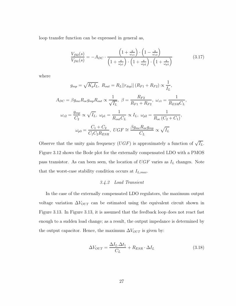
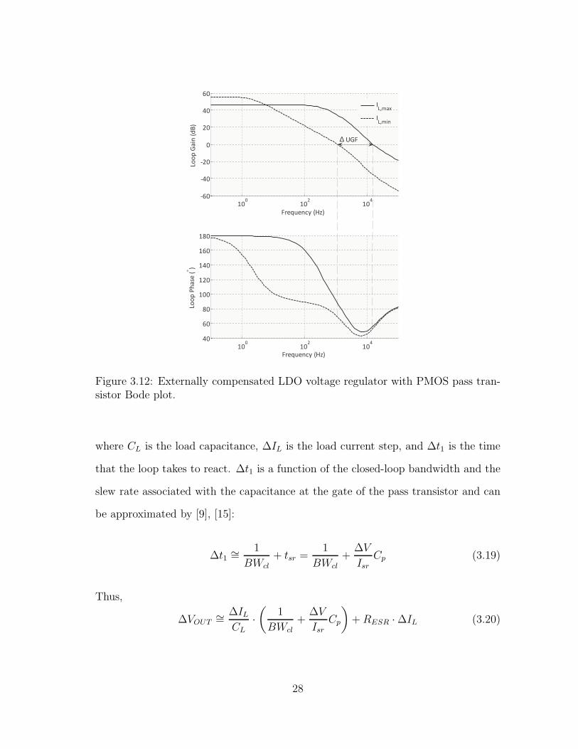
Figure 5.7 shows the closed loop block diagram of a voltage mode PWM buck
converter which includes a compensator, a carrier signal generator, a comparator, a
93
power stage, and an output filter.
Mn
Mp
L
CILOAD
H(s) Σ
VINVOUT
VREF-
+
Vc
Compensator
Vea
Vs
Power stageOutput filter
Carrier signal generator
Comparator
VSW
Figure 5.7: Block diagram of a buck converter with voltage mode PWM control.
This system operates as follows: If Vea is larger than the carrier signal voltage
(e.g. VOUT < VREF ), then Vc turns on and off Mp and Mn, respectively. This effect
causes the inductor current to increase and as a result VOUT also increases. The
opposite effect would occur if Vea is smaller than the carrier signal voltage (e.g.,
VOUT > VREF ).
When analyzing the stability of the loop, the combination of the carrier signal
generator, comparator, and power stage is typically referred to as the modulator,
and its gain is often assumed to be constant (VIN/Vs) [52]-[53].
Figure 5.8 shows the output filter including the parasitic resistances of the ca-
pacitor and inductor.
94
L
RESR
RDCR
C
VSW VOUT
Figure 5.8: Buck converter’s output filter with parasitics.
The transfer function of the output filter is given by:
F (s) =VOUT (s)
VSW (s)=
sCRESR + 1
LCs2 + (RESR +RDCR)Cs+ 1(5.16)
Hence, the overall open loop transfer function of the buck converter without com-
pensation block is given by:
H(s)open−loop =VIN
Vs· sCRESR + 1
LCs2 + (RESR +RDCR)Cs+ 1(5.17)
H(s)open−loop =VIN
Vs·
sωz
+ 1s2
ω2o+ 1
ωoQs+ 1
(5.18)
where
ωo =1√LC
, ωz =1
RESRC, Q =
1
RESR +RDCR
√
L
C(5.19)
Because the term (RESR + RDCR)C is usually small, the loop can be approximated
to have a double pole located at ωo = ωLC = 1/(√
LC)
and a zero at ωz = ωESR
1/(RESRC). Figure 5.9 depicts the Bode plot of the open loop transfer function.
95
The gain at low-frequencies is given by the modulator gain (VIN/Vs). After ωLC ,
-90
0
Ph
ase
(G
ain
(d
B
(rad/s)
-40dB/dec
(rad/s)
LC
-180ESR
-20dB/dec
-135
20log(VIN/Vs)
Figure 5.9: Open loop Bode plot without compensation block.
the gain starts to roll off at -40dB/decade and the phase quickly reaches -180. If
RESR is very small, which is typically the case for load transient and output ripple
voltage specifications, ωESR is located at high frequencies and it does not help to
compensate the loop. Thus, this system has poor phase margin and low DC-gain.
A compensator is necessary to boost the loop phase margin to counteract the effect
of the output filter’s complex poles located at fLC = 1/(
2π√LC)
and increase the
loop gain.
96
5.6.1.1 Type-I Compensation
A Type-I voltage mode compensator (an integrator) can be used to stabilize
the loop. This compensation scheme is simple since it only requires a resistor, a
capacitor, and an amplifier. However, the loop crossover frequency must be smaller
than fLC to guarantee good phase margin; and as a result, poor transient response
is expected. Figure 5.10 shows a possible implementation for a Type-I compensator.
VoVi
VREFA(s)
C1
R1
Figure 5.10: Type-I compensator implementation.
The transfer function of this network assuming an ideal amplifier is given by:
H(s) =Vo(s)
Vi(s)= − 1
R1C1s(5.20)
This transfer function has one low-frequency pole. The transfer function of the
system for a non-ideal amplifier A(s) = Ao /(1 + s/ωp0) is given by:
H(s) =Vo(s)
Vi(s)= − Ao
(
1 + sωp1
)
·(
1 + sωp2
) (5.21)
97
where
ωp1∼= 1
AoR1C1, ωp2
∼= ωp0Ao = GB (5.22)
Parameters Ao, ωo, and GB are the DC gain, dominant pole, and gain bandwidth
product of the amplifier. Figure 5.11 illustrates the Bode plot for (5.21). Notice that
Figure 5.11 is not drawn at scale and ωp2 typically occurs at high frequencies in a
good design.
90
-90
0
Ph
ase
(G
ain
(d
B
(rad/s)90°
(rad/s)
p1
-135
p2
-45
Figure 5.11: Type-I compensator Bode plot.
5.6.1.2 Type-II Compensation
A Type-II voltage mode compensator is another option in buck converters; how-
ever, the equivalent series resistance (RESR) of the output filter capacitor must be
relatively large to generate a low-frequency zero, given by fESR = 1/(2πRESRC), to
98
provide phase boost to achieve stability. Figure 5.12 shows a Type-II compensator
implementation. The transfer function of this network assuming an ideal amplifier
Vo
Vi
VREFA(s)
R2 C2
C1
R1
Figure 5.12: Type-II compensator implementation.
is given by:
H(s) =Vo(s)
Vi(s)= −
sωz1
+ 1
R1 (C1 + C2) s(
sωp2
+ 1) (5.23)
where
ωz1 =1
R2C2, ωp2 =
1
R2(C1C2)/(C1 + C2)
This transfer function has one low-frequency zero, one low-frequency pole, and one
high-frequency pole. The transfer function of the system for a non-ideal amplifier
A(s) = Ao /(1 + s/ωp0) is given by:
H(s) =Vo(s)
Vi(s)= −Ao ·
sωz1
+ 1(
sωp1
+ 1)
·(
sωp2
+ 1)
·(
sωp3
+ 1) (5.24)
99
where
ωz1 =1
R2C2, ωp1 =
1
AoR1 (C1 + C2), (5.25)
ωp2 =1
R2(C1C2)/(C1 + C2), ωp3 = ωoAo = GB (5.26)
Figure 5.13 illustrates the Bode plot for Type-II compensation network with
non-ideal amplifier. In Figure 5.13, it was assumed that ωp3 was located at high
frequencies and its effect was neglected. There are different approaches on where
to place the low-frequency zero and high frequency pole [52]-[53]. For instance, the
procedure suggested in [52], places the zero at half fLC and the high frequency pole
at fs/2. One issue with this compensation is that the RESR may vary significantly
90
-90
0
Ph
ase
(G
ain
(d
B
(rad/s)
90°
(rad/s)
z1 p2p1
Figure 5.13: Type-II compensator Bode plot.
over temperature, and stability could be degraded. Moreover, having a large RESR
would increase the output voltage ripple as well as the amplitude of the voltage dips
and surges during load transient events as shown in (5.6).
100
5.6.1.3 Type-III Compensation
Type-III compensation is typically used to increase the crossover frequency be-
yond fLC (but, it is limited to one-fifth of the switching frequency (fs) due to the
sampling effect). Type-III is also used to improve the phase margin in applications
where fast transient response and an output filter capacitor with small RESR are re-
quired [54]. The conventional Type-III compensation network shown in Figure 5.14
requires three capacitors, three resistors, and an amplifier A(s). The transfer func-
Vo
Vi
VREFA(s)
R2 C2
C1
R1
R3 C3
Figure 5.14: Conventional Type-III compensation.
tion of this network assuming an ideal amplifier is given by:
H(s)Conv =Vo(s)
Vi(s)=
−(
sωz1
+ 1)
·(
sωz2
+ 1)
R1(C1 + C2)s ·(
sωp2
+ 1)
·(
sωp3
+ 1) . (5.27)
where
ωz1 =1
R2C2, ωz2 =
1
(R1 +R3)C3,
101
ωp2 =1
R3C3, ωp3 =
1
R2(C1C2)/(C1 + C2).
This transfer function has two low-frequency zeros, one low-frequency pole, and two
high-frequency poles. The transfer function of the system for a non-ideal amplifier
A(s) = Ao /(1 + s/ωp0) is given by:
H(s)Conv =Vo(s)
Vi(s)= Ao ·
−(
sωz1
+ 1)
·(
sωz2
+ 1)
(
sωp1
+ 1)
·(
sωp2
+ 1)
·(
sωp3
+ 1)
·(
sωp4
+ 1) . (5.28)
where
ωz1 =1
R2C2, ωz2 =
1
(R1 +R3)C3, ωp1 =
1
AoR1 (C1 + C2), (5.29)
ωp2 =1
R3C3
, ωp3 =1
R2(C1C2)/(C1 + C2), ωp4 = Aoωpo. (5.30)
Figure 5.15 illustrates the Bode plot of the Type-III compensation network.
90
-90
0
Ph
ase
(G
ain
(d
B
(rad/s)
180°
(rad/s)
z1 z2 p2 p3p1
Figure 5.15: Conventional Type-III Bode plot.
102
In Figure 5.15, it is assumed that ωp3 is located at high frequencies, and its
effect is neglected. The zeros compensate for the phase lag of the output filter’s
complex poles. Large capacitors and resistors are often required to generate these
low-frequency zeros, and a high-bandwidth amplifier is required to avoid misplace-
ment of the high-frequency poles. There are different approaches on where to place
the two low-frequency zeros [52]-[53]. For instance, the procedure suggested in [52]
places one zero at fLC and the other one at half fLC . The two high frequency poles,
ωp2 and ωp3, are placed at fs/2 and fESR, respectively. The guidelines for placing
the poles and zeros in [52] give the following instruction:
1. Select a value for R1.
2. Select a gain (R2/R1) that shifts the open loop gain up to achieve the desired
crossover frequency. This allows the crossover frequency to occur in the fre-
quency range that the Type-III compensator has its second flat gain. This can
be achieved using the following equation:
R2 =fcfLC
· Vs
VIN· R1 (5.31)
3. Calculate C2 by placing zero fz1 at fLC/2:
C2 =1
πR2fLC(5.32)
4. Calculate C1 by placing pole fp2 at fESR:
C1 =C2
2πR2C2fESR − 1(5.33)
5. Place pole fp3 at fs/2 and zero fz2 at fLC . This can be accomplished using the
103
following equations:
R3 =R1
fs2fLC
− 1(5.34)
C3 =1
πR3fs(5.35)
5.6.2 Current Mode PWM Compensation
5.6.2.1 Peak Current Mode
Figure 5.16 shows a simplified block diagram of a buck converter with peak current
mode control. This compensation scheme has a fast inner loop (current loop) and a
Ri
Mn
Mp
L
KIL
C ILOAD
H(s) Σ
VINVOUT
VREF-
+
Vea
R
SQb
QVc
Vi
compensatorCLK
Vea
KILRi
Figure 5.16: Buck converter with peak current mode control block diagram.
slow outer loop (voltage loop). Notice that Vi is proportional to the inductor current,
and it generates the carrier signal for PWM.
The operation of this compensation scheme can be described as follows: At the
beginning of each cycle the clock signal (CLK) sets the SR-latch (Q=1, Qb = 0) to
104
turn on and off Mp and Mn, respectively. This effect causes the inductor current to
increase. When Vi = Vea, Vc resets the SR-Latch (Q=0, Qb = 1) to turn off and on
Mp and Mn, correspondingly. This makes the inductor current to decrease.
One advantage of current mode PWM over the conventional voltage mode PWM
is the line transient performance. This is due to the fact that the carrier signal Vi
during the on-time of Mp is proportional to VIN (i.e., VIN -VOUT ) and it provides a
pseudo feed-forward path [55].
Another advantage of current mode PWM over voltage mode PWM is that the
output filter transfer function behaves as a single pole (1/(RLC)) in the region of
interest [3]. This simplifies the compensation block (H(s)) when compared with Type-
III compensation scheme in voltage mode. In current mode, an H(s) implementation
with one zero can stabilize the loop. A typical implementation of the compensator
is shown in Figure 5.17.
RO
Rz
Cc
Gm
+
- Vout
VREFVea
Figure 5.17: A typical compensation implementation of H(s) for current mode con-trol.
105
The transfer function of this compensator is given by:
H(s) =Vea(s)
Vout(s)= −GmRo ·
sωz1
+ 1s
ωp1+ 1
(5.36)
where
ωz1 =1
RzCc, ωp1 =
1
(Rz +Ro)Cc
Ro represents the output resistance of the operational transconductance amplifier.
This transfer function has one low-frequency pole (ωp1) and one zero (ωz1). Typically,
ωp1 defines the dominant pole of the loop and ωz1 cancels or minimizes the effect of
the output filter pole (1/RLC).
One drawback of peak current mode control is that when D > 0.5, the converter
suffers from subharmonic oscillation [3]. This effect is explained in [3], and it can
be solved by adding a compensating slope. This compensation slope complicates the
design and increases the quiescent power consumption. Another disadvantage is the
noise sensivity, particularly if the inductor ripple current is small [56].
5.6.2.2 Current Sensing Techniques
In this section, several current sensing techniques are presented. Current sensing
techniques can be used to measure the inductor current for current mode control or
over-current protection [57].
5.6.2.3 Series Sense Resistor
The series sense current sensing method is shown in Figure 5.18. If the value of
Rs is known, the inductor current can be measured by sensing the voltage across the
resistor (Vs). The accuracy of Rs determines the accuracy of this method. An exces-
sively small value of Rs could be comparable to parasitic board/package resistances,
thereby reducing measurement accuracy. Moreover, Vs needs to be large enough to
106
Mp
Mn
L Rs
C
Vs+ -
Vo
Vi
IL
Figure 5.18: Series sense resistor.
overcome the input referred offset of the sense amplifier for practical reasons [57].
Nevertheless, a very large value of Rs would degrade the efficiency of the system
since it has the same effect as the DCR of the inductor. This method is undesirable
in low-voltage high-current applications where conduction losses are critical.
5.6.2.4 Filter Sense Inductor
In this technique, an RC filter is placed in parallel with the inductor as shown in
Figure 5.19. The voltage across the inductor (VL) is given by:
VL = VSW − Vo = IL · (L · s+DCR) = IL ·DCR ·(
L
DCRs+ 1
)
(5.37)
From Figure 5.19, the voltage across capacitor Cc is then given by:
Vc =VL
1 + sRcCc= IL ·DCR ·
(
LDCR
s+ 1
1 + sRcCc
)
(5.38)
107
Mp
Mn
L DCR
C
Vc+ -
Vo
Vi
IL
Rc Cc
VL+ -
VSW
Figure 5.19: Filter sense the inductor.
If the pole 1/(RcCc) is placed at the same frequency of the zero (DCR/L), then Vc
is proportional to IL:
Vc = IL ·DCR (5.39)
This technique is popular because it is relatively lossless when compared with the
sense series resistor technique and has good accuracy [47]. A drawback of this tech-
nique is that the values of DCR and L need to be known, to select the values of Rc
and Cc properly. In addition, it is difficult to have an integrated version of this tech-
nique due to the size of Rc and Cc and the required tolerance of the components [57].
5.6.2.5 Sense Fets
Figure 5.20 shows the sense FET current sensing technique. In this technique,
a current sensing transistor Ms is placed in parallel with the power transistor Mp.
Notice that both transistors share the gate and source, and the effective width of
Ms is K times smaller than Mp. Hence, Is is a scaled version of Ip. K is usually
108
Mn
L
C
Vo
Vi
IL
Ms
As
RsVs
+
-
Mp
1:K
Vsw
Va
Loop Is
Ip
(W/L)(1/K)(W/L)
Figure 5.20: Sense Fet method.
larger than 100 to minimize the quiescent power consumption for large Ip. Amplifier
As is added to make Vsw = Va to minimize channel length modulation and improve
current mirror accuracy. The stability of the loop needs to be guaranteed for this
technique to operate properly. Moreover, the loop bandwidth should be large enough
to include the high frequency components of Ip. Hence, voltage Vs is proportional to
Ip:
Vs = Is ·Rs =
(
IpK
)
· Rs (5.40)
This particular implementation only contains the positive slope information of the in-
ductor current and hence, it is useful for peak current mode control and over-current
protection. If both slopes of the inductor current are required, another sense tran-
sistor can be added in parallel with Mn to obtain the negative slope of the inductor
current [51], [58]. This technique is appropiate for an integrated implementation.
109
5.6.3 Hysteretic Compensation
Hysteretic compensation is also known as bang-bang control [59]. A block di-
agram of a buck converter with hysteretic voltage mode control is illustrated in
Figure 5.21. Notice that this topology is very simple, and its implementation does
Mp
Mn
L
C
IL
Vi Vo
RESR
Buffer
+
Non-Overlapping
CircuitVH
VL
Hysteretic
comparator
t
VH
VL
Vo
Vc
VcH
Vc
VIN
VcL
VL VH
Figure 5.21: Block diagram of a buck converter with hysteretic compensation.
not require resistors or capacitors for compensation. Moreover, this topology does
not use the amplifier and carrier signal generator utilized in PWM topologies. This
significantly reduces the quiescent power and as a result, this architecture can achieve
high efficiency at light loads [59]. In addition, this compensation scheme can react
to load transient events in the same cycle that they occur [60]. One drawback of
this compensation is that fs is variable. This variation in fs makes electromagnectic
interference (EMI) shielding in electronics equipment difficult [61]. The operation of
110
this system can be described as follows: if Vo > VH , then Vo is discharged by turning
off Mp and turning on Mn. If Vo < VL, then Vo is charged by turning on Mp and
turning off Mn. Hence, Vo is always between VH and VL, and the average value of Vo
is VL + (VH-VL)/2. Assuming that output voltage ripple (∆vo) is only due to RESR,
∆vo = VH − VL = RESR ·∆iL (5.41)
where
∆iL =(Vi − Vo) Vo
ViLfs(5.42)
From (5.41) and (5.42), fs is found to be:
fs =Vo (Vi − Vo)RESR
ViL(VH − VL)(5.43)
where (VH - VL) is the hysteresis window of the comparator. As can be observed
the switching frequency depends on the output filter components, input and output
voltage, and hysteresis window. Also, notice that the switching frequency is propor-
tional to RESR. This could be an issue since typically capacitors with small RESR are
required for load transient purposes but this makes fs very low. Equation 5.43 does
not include the effects of the C, equivalent series inductance (ESL), or the delay due
to the comparator and drivers on the output voltage ripple. These effects complicate
fs estimation and control [62]. A modified hysteretic controller has been proposed
in [60] to minimize the dependency of fs on the output capacitor and its parasitics
(RESR, ESL). Nevertheless, this technique increases the cost of the system since it
requires two additional capacitors and a resistor. A possible implementation of the
hysteretic comparator is shown in Figure 5.22 [59]. Signal Q is used to control the
power transistors. If VIN > VH , then Sbar = 0, Rbar = 1, and Q = 1. If VL < VIN <
111
VH , then Sbar = 1, Rbar = 1, and Q = Qprev. Finally, if VIN < VL, Sbar = 1, Rbar =
0, and Q = 0.
Q
Qn
VH
VL
VIN
Sbar
Rbar
Figure 5.22: Hysteretic comparator.
5.6.4 Sliding Mode Control Compensation
Sliding mode control (SMC) was first proposed in the 1950’s in the Soviet Union.
SMC is mostly used in systems with variable structures. Switching converters are
examples of systems with variable structures because during each subinterval of oper-
ation, the differential equations describing the system change. Sliding mode control
provides rejection to external perturbations, robustness to parameter variations, and
relatively simple implementations [63]–[66]. Figure 5.23 depicts the block diagram
of a buck converter implemented with sliding mode control.
The converter is a tracking system that minimizes the voltage error (Ve = VREF -
VOUT ) with the sliding mode controller. Notice that this topology does not require
the carrier signal generator utilized in PWM topologies and as a result, area and
quiescent power consumption are reduced.
The design of the sliding mode controller is based on the state variables of the
desired system to be controlled. In the case of the buck converter, the low-pass
112
Mp
Mn
L
CIL
VIN VOUT
Buffer
+
Non-Overlapping
CircuitVH
VL
Hysteretic
comparator
Vc
Sliding Mode
ControllerΣ
VREF
-
+
Ve
VSW
Figure 5.23: Block diagram of a buck converter implemented with sliding modecontrol.
filter and the power switches are used for the analysis. In Figure 5.24, two different
structures can be observed during one cycle of operation.
During the first subinterval (Figure 5.24 (a)), Mp is closed and Mn is open, hence
VSW = VIN . During subinterval II (Figure 5.24 (b)), Mp is open and Mn is closed,
thus VSW = GND. The SMC generates a control function, i.e., control law/switching
function (SF), to stabilize the system. The control function makes the system switch
between its different structures until the system reaches its sliding equilibrium point
(SEP) [64]-[66]. The buck converter is designed to have an SEP is given by:
SEP = (VREF , IOUT ) (5.44)
For example, Figure 5.25 shows the phase portraits for both structures when VREF
= 0.9 V and IOUT= 50 mA. The phase portrait in Figure 5.25 (a) corresponds to
113
Mp
Mn
L
C IL
VIN
VOUTVSW
(a) (b)
Mp
Mn
L
C IL
VIN
VOUTVSW
Figure 5.24: Subintervals in a buck converter (a) subinterval I (b) subinterval II.
structure I in Figure 5.24(a). This portrait represents the trajectories of the dynamic
system modeled when VSW = VIN . Each trajectory represents the motion of the state
space variables vC2 and iL2 in the phase plane. Even though structure I converges to
a stable focus equilibrium point [64]-[66], it does not converge to the desired SEP (0.9
V, 50 mA). Similarly, the phase portrait in Fig. 5.25 (b) corresponds to structure II,
in Figure 5.24 (b), when the VSW = GND. As in the previous case, structure II does
not converge to the SEP. Therefore, a controller is necessary because the SEP is never
reached. By designing an appropiate SMC, the SF will make the system to toggle
between both structures, creating a sliding surface. In other words, regardless of the
initial conditions, the dynamics of the system would move toward the sliding surface
until they hit it. Once there, the system will slide in direction of the equilibrium
point. Figure 5.26 illustrates the phenomenon.
114
0 0.5 1 1.5 2
−0.6
−0.4
−0.2
0
0.2
0.4
0.6
0.8
vC2
(V)
i L2 (
A) (1.8, 0.1)
(a)
0 0.5 1 1.5 2
−0.6
−0.4
−0.2
0
0.2
0.4
0.6
0.8
vC2
(V)
i L2 (
A)
(0.0, 0.0)
(b)
Figure 5.25: Phase portraits of VOUT (a) phase portrait of structure I and (b) phaseportrait of structure II.
The SF of the sliding mode controller is defined as:
S(Ve, s) = (1 + αs)Ve(s) (5.45)
where α is calculated to meet the Hurwitz stability criterion and to guarantee a
smooth and fast transient response [64]-[66].
In general, for a kth-order system, sliding mode theory requires a (k − 1)th-order
controller [63]-[66]. Since the buck converter is modelled as a second-order system,
115
0 0.5 1 1.5 2
−0.6
−0.4
−0.2
0
0.2
0.4
0.6
0.8
vC2
(V)
i L2 (
A) (0.9, 0.05)
Figure 5.26: Phase portrait of the controlled system trajectories of VOUT undersliding-mode operation.
the controller dynamics are defined by a first-order equation. The switching function
is defined as the sum of Ve and its derivative multiplied by a constant. The system
can be proved to be asymptotically stable [63]-[66] since the sliding equilibrium point
is a stable node with an eigenvalue that is real and negative. The SMC would make
each subsystem switch according to the sign of the SF as:
VSW =
VIN when s(Ve, t) > 0
0 when s(Ve, t) < 0(5.46)
5.6.5 Digital Control Compensation
Digital PWM control has several advantages over analog control such as: ro-
bustness to parameter variations, programmability, and reduction or elimination of
external passive components for compensation, and calibration [67]. Figure 5.27
shows a block diagram of a buck converter with digital PWM control. As can be
seen from Figure 5.27, digital PWM control consists of an analog to digital converter
(ADC), a digital filter (compensator), and a digital PWM (DPWM). This circuit
116
Mn
Mp
L
CILOAD
A/D
ConverterΣ
VIN
VOUT
VREF-
+
Compensator
Power stageOutput filter
Digital
Filter
Vee[n]Digital
PWM
dc[n]
Buffer
npwm
Digital PWM Controller
Figure 5.27: Block diagram of a buck converter with digital control.
operates as follows: The voltage error, Ve = VREF -VOUT , is sampled and converted
to a digital error signal e[n] by the ADC. Then, the digital filter calculates the digital
duty-cycle dc[n] command, and the DPWM generates a signal with the desired fs
and duty cycle to control the power stage.
There are some challenges in the implementation of a digital PWM control; for
example, the ADC conversion time should be in the order of 100 ns for switching
frequencies in the MHz range [67]. In addition, an ADC with a resolution of 6 bits
or more is typically required to achieve good voltage regulation. An ADC with this
kind of performance could consume more power and chip area than the entire analog
controller. Delay-line based windowed ADC has been proposed to tackle the power
consumption issue [68]. The resolution of the DPWM must be higher than the one of
the ADC to avoid limit-cycle oscillations and as a result, high power consumption is
typically required in the DPWM. A survey of possible DPWM implementations for
digital control of switching DC-DC converters is offered in [69]. In general, a buck
117
converter implemented with digital PWM control consumes higher power than one
implemented with analog control [70].
5.6.6 Compensation Scheme Summary
Table 5.2 summarizes the advantages and disadvantages of each compensation
scheme presented in this section.
Table 5.2: Summary of advantages and disadvantages of the different compensationschemesCompensation scheme Advantages Disadvantages
Voltage Mode PWM Constant fs, predictable EMI, Area by compensation components,(Type-III) good load transient response, Complicated compensation
predictable performance
Current Mode PWM Inherent current protection, Sub-harmonic oscillation for D > 0.5,(Peak) good transient, first-order Noise sensitivity for small inductor
system, simpler compensation current ripple and light loads,constant fs complexity
Hysteretic Fast transient response, no Variable fs, Unpredictable EMI,passive compensation components,small quiescent power
Sliding Mode Fast transient response, few Variable fs, Unpredictable EMIpassive compensation components,small quiescent power
Digital Robustness to parameter Quiescent power consumption,variation, programmability, areareduction or elimination ofexternal passive components,calibration
5.7 Multiphase Interleaved Buck Converter
Figures 5.28 shows the block diagram of a multiphase interleaved buck con-
verter [71]. A multiphase buck converter combines N number of individual buck
converters with phase shift in parallel with common input and output connections.
118
The main advantage of multiphase buck converters is the output current ripple re-
duction which consequently decreases the output voltage ripple. This allows the use
of smaller inductance to improve load transient performance [72] since smaller in-
ductors provide a higher output current slew rate (di/dt = VL/L), where VL is the
inductor voltage. It also reduces the value of the required output capacitance [72]-
[73]. In this topology, every stage is operating at fs but the drivers are synchronized
∗ Part of this section is reprinted with permission from “Design of an integrated single-input dual-output 3-switch buck converter based on sliding mode control” by M. A. Rojas-Gonzalez, J. Torres, and E. Sanchez-Sinencio, Analog Integrated Circuits and Signal Process-ing, vol. 76, no. 3, pp. 307-319, September 2013.
132
converter. This section introduces several area reduction techniques for the buck
converter, which apply to its output filter, output power stage, and compensator.
Firstly, the design of a fully integrated buck converter using a standard 0.18 µm
CMOS technology is presented. The converter employs a dual-phase structure to
minimize the output voltage ripple. The controller is implemented using a hysteretic
architecture based on sliding-mode theory. The external low pass filter has been
integrated on-chip by increasing the switching frequency up to 45 MHz.
Secondly, the design and implementation of a single-input dual-output buck con-
verter is presented. The proposed topology implements only three switches instead
of the four switches used in the conventional solution, thus potentially reducing area
in the power stage through proper design of the power switches.
Thirdly, a compensation scheme that employs a combination of Gm-RC and
Active-RC techniques to emulate the conventional voltage mode Type-III compensa-
tion is proposed. This compensator reduces area by more than 45 % when compared
with the conventional Type-III compensator, while consuming low quiescent power
and achieving good line/load regulation. The total active area of the buck converter
is decreased by approximately 15%. Finally, conclusions are provided.
6.2 Buck Converter Output Filter Area Reduction
In low power applications, traditional buck converter implementations integrate
the compensator, carrier signal generator, comparator, and power stage; however,
the output filter is typically implemented with off-chip components due to their large
size. Typical switching frequencies are in the order of hundreds of kilohertz to a few
megahertzs. At such frequencies, the values of the filter inductor and capacitor are
in the order of µH and µF, respectively [2]. These values restrict the full integration
of the switching converter.
133
A fully-integrated buck converter would reduce the number of off-chip components
and printed circuit board (PCB) area, thereby significantly reducing the total cost of
the system. In addition, energy losses can potentially be minimized due to a reduction
in the interconnection parasitics between the integrated circuit (IC) and the external
components. Hence, it is necessary to reduce the filter inductor and capacitor to the
order of nH and nF, respectively. This can be achieved by increasing the switching
frequency to the order of tens of megahertz [2]. However, several key drawbacks such
as the effect of a low quality factor inductor (large parasitic resistance) and high
switching frequency in the efficiency performance need to be addressed. For more
details about how these factors affect the buck converter efficiency see section 5.5.
6.2.1 Multi-Phase Interleaved Buck Converter
Integrating LC-filter passive components demands a higher switching frequency
to obtain sufficiently small components values. The value of the output filter inductor
L and the output filter capacitor C in Figure 6.1, assuming CCM operation [2] are:
L =VIN (1−D)D
2∆iLfs(6.1)
C =∆iL
8∆vCfs(6.2)
where D, fs, ∆ iL, ∆ vC represent the duty cycle, the switching frequency, the
inductor current ripple, and the output voltage ripple, respectively.
However, due to dynamic losses proportional to the frequency of operation [2],
increasing the switching frequency degrades the switching regulator’s efficiency. A
possible solution to this drawback is the use of an interleaved synchronous converter
operating at lower frequency in parallel configuration, e.g., multi-phase structure [83]-
[84].
134
A multi-phase buck converter is the combination of many individual buck con-
verters sharing the same load. These converters are connected in such way that
the current they deliver adds to the output node. Moreover, output ripple can be
reduced if the drivers of each stage are synchronized such that adjacent phases are
better conductivity and/or magnetic materials could boost the quality of the output
inductor. In [83], high-quality aircore inductors are utilized to minimize conduction
power losses, and a special top metal layer based on copper have been used in [84]
to improve the quality factor of the inductor. Moreover, a CMOS compatible micro-
electromechanical (MEM) technique to built air-core plastic deformation magnetic
assembly (PDMA) inductors is utilized in [89]. Inductors in [90] use magnetic ma-
terials to improve the quality factor. A commercial product in [91] uses on-package
inductors, but the capacitor is external. Package bondwires have a very good quality
factor and have been employed to improve the efficiency of a buck converter in [92].
Nevertheless, this implementation may be unreliable due to the inductance variation
of a bondwire. All these previous works utilize expensive post-fabrication techniques
or high-cost special fabrication processes to produce a good quality inductor, while
the proposed implementation utilizes a low-cost fabrication process.
6.2.4 Simulation Results
Figure 6.5 shows the layout of the buck converter. The size of the proposed
converter is 2.5 mm x 4 mm. The output capacitor and the output inductor occupy
more than 90% of the total area. The efficiency of the buck converter, including
schematic and postlayout simulations, is presented in Figure 6.6. Process corner
simulations performed on the voltage regulator yielded a variation in efficiency of
139
Capacitor CapacitorSMC
C
RS
Power Stage
L2L1
Capacitor
4.0 mm
2.5
mm
Figure 6.5: Layout of the proposed fully-integrated buck converter.
0 0.05 0.1 0.15 0.2 0.25 0.3 0.35 0.40
10
20
30
40
50
60
POUT
(W)
η (%
)
SchematicPostlayout
Figure 6.6: Efficiency versus POUT of the proposed buck converter.
only ±5%. The anticipated QL of the designed inductor is approximately 3. The
converter was also simulated for the hypothetical case of having a thicker top metal
layer (higher QL). As QL increases, the equivalent series resistance drops, and the
efficiency of the buck converter increments by more 10% from its original value as
shown in Figure 6.7. The load transient response of the buck converter for a 100
mA step is shown in Figure 6.8.
140
3 5 8 1250
52
54
56
58
60
62
64
QL
η (
%)
IOUT = 200 mA
Actual QL
Figure 6.7: Efficiency versus QL.
0.7 0.8 0.9 1 1.1 1.2 1.3 1.4
x 10−6
0.9
0.95
1
1.05
1.1
1.15
Time (s)
Vol
tage
(V
)
Figure 6.8: Output voltage variation for a current step from 100 mA to 200 mA andvice versa.
141
6.3 Buck Converter Power Stage Area Reduction
The implementation of multiple supply voltages in a given electronic product has
become mandatory. A typical system as shown in Figure 6.9 requires the interaction
of different subsystems, each one of them fabricated in a different technology pro-
cess and with particular voltage specifications [2], [93]-[94], thus requiring multiple
supply-voltage levels. There are circuits using newer technologies and lower voltage
DC-DC
Converter #1Display
Disk drive
Microprocessor
VDD1
VDD2DC-DC
Converter #2
DC-DC
Converter #3
VDD3
Vsource
System
Figure 6.9: Multiple supplies on a typical system.
levels along with circuits using legacy power supplies and higher voltage levels [95].
Furthermore, using multiple supply voltages in digital circuits has significantly re-
duced dynamic power dissipation [96]. A dual power supply can reduce the dynamic
power dissipation by employing a lower voltage in non-critical blocks and higher levels
in critical paths, without compromising the overall circuit performance [2], [97]-[98].
Delivering multiple voltage levels requires the same number of switching convert-
ers, thus increasing component count and power stage area [99]. Previous solutions
to this problem proposed sharing the output inductor in the low-pass filter to gener-
142
ate multiple output voltages [95], [100]. However, this method may present problems
because one single inductor must store and deliver different levels of energy to each
output. In this work, we propose a proof-of-concept dual-output buck converter with
reduced number of switching elements in the power stage [93], [94] to demonstrate
that the proposed solution can be feasible, reliable, cheap, and versatile.
6.3.1 Multiple-Output Buck Converter
A conventional synchronous buck converter architecture requires a pair of switches
[3], thus generating n output voltages requires 2n switches. On the other hand, the
proposed buck converter [93]-[94] implements only n + 1 switches for n outputs.
The reduction in the number of switches reduces the amount of area and the number
of external components, thus reducing the total cost of the system [93]-[94].
6.3.2 Dual-Output Operation
Figure 6.10 shows the basic schematic diagram of the dual-output buck converter
and its modes of operation. The steady-state operation of the regulator has n + 1
subintervals for n outputs. For this specific case, a complete cycle of operation
consists of three different subintervals.
During subinterval I, shown in Figure 6.10 (a), the switches T1 and T2 are closed,
and switch T3 is open. The current flows from the power supply through the in-
ductors toward the output nodes. Since the converter requires VOUT1 ≥ VOUT2 for
proper operation, the length of the first subinterval sets the duty cycle of VOUT2.
In subinterval II, illustrated in Figure 6.10(b), switch T1 remains closed, switch T2
opens, and switch T3 closes. The duration of subinterval I plus that of subinterval
II determines the duty cycle for VOUT1 (D1 ≥ D2). Lastly, during subinterval III,
depicted in Figure 6.10(c), switch T1 opens, switch T2 closes again, and switch T3 re-
mains closed. Figure 6.11 sketches the necessary non-overlapping signals to operate
143
L1 iL1
C1 R1vC1
VOUT1
VDD
T1
T2
PWM1
L2 iL2
C2 R2vC2
VOUT2
T3
PWM2
L1 iL1
C1 R1vC1
VOUT1
VDD
T1
T2
PWM1
L2iL2
C2 R2vC2
VOUT2
T3
PWM2
L1iL1
C1 R1vC1
VOUT1
VDD
T1
T2
PWM1
L2iL2
C2 R2vC2
VOUT2
T3
PWM2
(a) (b) (c)
Figure 6.10: Schematic diagram of the dual-output buck voltage regulator and itsoperating modes (a) subinterval I (b) subinterval II and (c) subinterval III.
0 TI II III
G1
G2
G3
Figure 6.11: Sequence of non-overlapping operating signals applied to T1, T2, andT3, in the dual-output buck voltage converter.
the dual-output buck converter. Signals G1, G2, and G3, are applied to switches T1,
T2, and T3, respectively.
The proposed converter was fabricated using 0.5 µm standard CMOS technology,
operates with a voltage supply of 1.8 V, generates 1.2 V and 0.9 V, and supplies
a maximum current of 200 mA (100 mA provided by each output). The switching
frequency is 500 kHz. The current ripple ∆i, and the voltage ripple ∆v are 5% of the
maximum current and 1% of the higher output voltage, respectively. The inductors
The second-stage(M4-M5) is required to achieve nearly rail-to-rail output voltage
swing and provide a Class-AB type of driving capability. The current consumption
is approximately 1.3 µA.
6.4.2.4 Carrier Signal Generator
The carrier signal generator, shown in Figure 6.22, was implemented using the
circuit shown in Figure 6.30. The frequency of this circuit is determined by the
input square waveform which operates at 1 MHz with 50% duty cycle (D) and it is
168
Vdd
R
C
IB
~|Vdd|
Ts
Ms
Vc
Toff Ton
Figure 6.30: Carrier signal generator implementation.
generated externally in this prototype. During Toff , transistor Ms is off, and the
current source IB charges the output capacitor C linearly. During Ton, transistor
Ms is on, and C is discharged exponentially through R. The peak-to-peak voltage
amplitude of the carrier signal can be expressed as,
Vc,pp =ToffIB
C, (6.20)
where
Toff = (1−D)Ts. (6.21)
Applying capacitor charge balance [3], the average voltage of the carrier of the carrier
signal can be found to be:
Vc,avg =RIBD
, (6.22)
where D is the duty cycle of the input square waveform. It is important to choose
an appropiate average voltage since it sets the input common mode voltage of the
comparator and the output common mode voltage of the compensator circuit.
If the value of the chosen R is large enough, a quasi-linear negative slope is
169
40 40.5 41 41.5 42 42.5 430.6
0.65
0.7
0.75
0.8
0.85
0.9
0.95
1
1.05
Time (µs)
Mag
nitu
de (
V)
T=1µs
A=360mV
Figure 6.31: Carrier signal waveform.
achieved as shown in Figure 6.31. The THD of the waveform shown in Figure 6.31
is approximately 13.36 dB, while the THD of an ideal triangle wave is 12.22 dB.
The values of IB, R , and C were chosen to be 2 µA, 213.5 kΩ, and 2.8 pF, respec-
tively. For the chosen values, Vc,pp and Vc,avg are approximately 357 mV and 854
mV, respectively. The modulator gain GM can be approximated as [3], [52]-[53],
GM =Vin
Vc,pp, (6.23)
where Vin is the input voltage of the buck converter (see Figure 6.1). For an input
voltage of 1.8 V, GM is approximately 14 dB. The proposed carrier signal generator
can be designed using the following procedure:
1. Select the peak-to-peak amplitude for the carrier signal generator (Vc,pp) to
170
achieve a desired modulator gain:
Vc,pp =Vin
GM(6.24)
2. Select a value for IB and then calculate C using the following equation (this
assumes that Ts and D were previously defined):
C =(1−D) TsIB
Vc,pp(6.25)
3. Select the desired common mode voltage Vc,avg and calculate R:
R =DVc,avg
IB(6.26)
6.4.2.5 Power Stage Implementation
Figure 6.32 shows the implemented power stage block diagram. The power FETs
(MP and MN ) were designed to minimize the conduction losses by reducing the
CMOS on-resistance Ron. The dimensions of the PMOS power switch (MP ) are W
= 25000 µm and L = 0.18 µm, and the dimensions of the NMOS power switch (MN)
are W = 12500 µm and L = 0.18 µm.
The driver stage was optimized to minimize the gate drive power losses without
degrading the propagation delay, and the short circuit current was reduced with
a non-overlapping configuration [111]. The functions of drive and non-overlapping
time are implemented separately; the buffers are in the forward path, and the delay
elements are in the feedback path as shown in Figure 6.32. By doing this, the
buffers can be designed in a compact fashion with low power consumption and the
delay elements can be designed independently without affecting the delay of the
171
Delay 2
Delay 1
MP
MN
VIN
Power FETs
PMOS Buffer
NMOS Buffer
Driver stage
VSW
VC
Figure 6.32: Power stage block diagram.
forward path. The non-overlapping time should be small enough that it does not
degrade the overall efficiency but large enough to deal with process variation [112].
Based on simulation results and considering these design trade-offs, a non-overlapping
time of 8 ns was chosen. Delay 1 element was implemented with 6 inverters and
Delay 2 element with 7 inverters. Even with the delay block placed in the feedback
path, the forward driving path should be designed taking into consideration the
trade-off between the delay and power consumption. For the smallest propagation
delay, the optimized scale factor between stages is mathematically equal to Euler’s
number [79]; however, it requires an impractical number of stages which increases
area and switching power consumption. Therefore, for the PMOS driver, a scale
factor of 20 was used for the last buffer stage, and 7, 6, and 5 for the previous stages,
respectively. For the NMOS driver, the scale factors are: 15, 10, and 8 for the third,
second, and first inverter, correspondingly. As a result, the gate driver power losses
are reduced and the system achieves high efficiency over a large output power range.
172
6.4.2.6 Output Filter Implementation
The second-order low-pass filter consists of two capacitors in parallel of 4.7 µF
with an RESR of 10 mΩ each, and an inductor of 2 µH. The transfer function of the
output filter is given by:
H(s)filter =sωz
+ 1s2
ω2o+ 1
ωoQs + 1
(6.27)
where
ωo =1√LC
, ωz =1
RESRC, Q =
1
RESR + 2RDCR
√
L
C(6.28)
These components generate complex poles at a frequency similar to the ones
generated by an output filter with a capacitor of 4.7 µF and an inductor of 4.7
µH [107]. However, the proposed component values reduce the output impedance
of the buck converter [106], [113] and as result, for given current step during load
transient, the amplitude of the voltage dips and surges are smaller with the proposed
configuration.
6.4.3 Experimental Results
The proposed buck converter was fabricated in 0.18 µm CMOS standard tech-
nology. The chip prototype was encapsulated in a QFN 28 package. Figure 6.33
shows the die micrograph of the fabricated buck converter where blocks I, II, and III
correspond to the compensator, comparator and carrier signal generator, and power
stage, respectively. The total active area occupied by the buck converter is 0.1325
mm2. The prototype was tested for an input voltage of 1.8 V and an output volt-
age of 0.9 V. Table 6.4 summaries the performance of the prototype and compares
it to that of the state-of-the-art voltage mode buck converters operating at 1 MHz
switching frequency.
173
I
II
III
1.301 mm
1.3
28
mm
Figure 6.33: Buck converter die micrograph, I compensator (0.0985mm2), II com-parator and carrier signal generator (0.0073mm2), and III power stage (0.0267mm2).
0 100 200 300 400 50070
75
80
85
90
95
100
Effi
cien
cy (
%)
Pout
(mW)
Figure 6.34: Efficiency versus output power.
174
Table 6.4: Buck converter performance summaryParameters [107] [114] [115] This Work
Switching frequency 1 MHz 1 MHz 1 MHz 1 MHzMaximum output current 600 mA 800 mA 500 mA 550 mAMaximum power efficiency 97% 96% 90% 96%
Compensator quiescent current 30 µA - - 8.8 µAOutput ripple voltage < 10 mV 35 mV - < 5 mV
[147] Y. Choi, W. Tak, Y. Yoon, J. Roh, S. Kwon, J. Koh, “A 0.0018% THD+N,
88-dB PSRR PWM class-D amplifier for direct battery hookup,” IEEE Journal
of Solid-State Circuits, vol. 47, no. 2, pp. 454-463, February 2012.
[148] V. Utkin, “Variable structure systems with sliding mode,” IEEE Transactions
on Automatic Control, vol. 22, no. 2, pp. 212-222, April 1977.
[149] H. K. Khalil, Nonlinear Systems, 3rd Edition, Upper Saddle River, New Jersey:
Prentice Hall, 2002.
236
[150] K. Ogata, Modern Control Engineering, 3rd Edition, Upper Saddle River, New
Jersey: Prentice Hall,1998.
[151] R. C. Dorf and R. H. Bishop, Modern Control Systems, 10th Edition, Upper
Saddle River, New Jersey: Prentice Hall, 2005.
[152] C. Chen, Linear System Theory and Design, 3rd Edition, New York: Oxford
University Press, 1999.
[153] F. B. Cunha, D. J. Pagano, and U. F. Moreno, “Sliding bifurcations of equi-
libria in planar variable structure systems,” IEEE Transactions on Circuits and
Systems I, vol. 50, no. 8, pp. 1129-1134, August 2003.
237
APPENDIX A
LDO VOLTAGE REGULATOR PERFORMANCE DEFINITIONS
This appendix provides low drop-out voltage regulator performance definitions.
• Stability: it is quantified by measuring the phase margin at the loop’s unity
gain frequency.
• Load transient: quantifies the peak output-voltage excursion and signal set-
tling time when the load-current is stepped.
• Load regulation: quantifies the voltage variation at the output when a change
in the load-current happens but it is measured once the output voltage is in
steady-state.
• Power supply rejection: refers to the amount of voltage ripple at the output
of the LDO coming from the ripple at the input.
• Line transient: measures the output voltage variation in response to a voltage
step at the input of the LDO regulator.
• Line regulation: quantifies the voltage variation at the output when a change
in the input voltage happens but it is measured once the output voltage is in
steady-state.
• Noise: refers to the thermal and flicker noise in transistors and resistors in
LDO voltage regulator .
• Drop-out voltage: it is the minimum difference between the input and
output volt- ages at which the circuit ceases to regulate.
238
• Quiescent current: it is the difference between the input current of the LDO
voltage regulator and load current.
• Efficiency: it is defined as the ratio of the output power over the input power.
239
APPENDIX B
FUNDAMENTALS OF SLIDING MODE CONTROL∗
This appendix presents the fundamentals of sliding mode control (SMC) theory.
It begins with an introductory example to illustrate its principles of operation, and
to highlight its main characteristics. Additionally, a formal description of the sliding
mode controller, and the switching function, is given. Furthermore, the analysis
of stability, based on the Lyapunov function approach and the equivalent control
approach, is explained. Finally, the derivation of the switching function and the
stability proof, for the particular case of the second-order low-pass filter employed in
the design of the systems described in this dissertation, are detailed.
B.1 An Introductory Example
The first developments of sliding mode control (SMC) occurred in the 1950s as
a consequence of the analysis of discontinuous variable structure systems (VSS). A
variable structure system consists of a set of continuous subsystems together with a
switching logic. Therefore, the variable structure control (VSC) with sliding modes
consists on selecting the parameters of each one of these substructures to define the
switching logic of the system. The most outstanding feature of variable structure
control is its ability to result in very robust control systems, insensitive to parametric
uncertainty, and external disturbances [63], [85], [148], [149].
The basic idea of variable structure control with sliding modes, or simply sliding
mode control, can be illustrated by analyzing the second order system shown in
∗Reprinted with permission from “Design and implementation of switching voltage integrated cir-cuits based on sliding mode control,” by M. A. Rojas-Gonzalez, Ph.D Dissertation, Texas A&MUniversity, August 2009.
240
∫ ∫Σx1(t)
2
1
x2(t)u(t)
Figure B.1: Model of a simple variable structure system.
Figure B.1. The system can be expressed in terms of its state variables as
ddtx1(t)
ddtx2(t)
=
0 1
−1 2
x1(t)
x2(t)
+
0
1
u(t) (B.1)
where
u(t) =
4 when s(x1, x2, t) > 0
−4 when s(x1, x2, t) < 0(B.2)
and s(x1, x2, t), defined as
s(x1, x2, t) = x1(t)
(
1
2x1(t) + x2(t)
)
(B.3)
represents the switching function, which will be defined later in the appendix.
Therefore, the second-order system, in equation (B.1), is analytically defined in
two regions of the phase plane, i.e. the x1-x2 plane, by two different mathematical
241
models. The first model, when s(x1, x2, t) < 0, is
ddtx1(t)
ddtx2(t)
=
0 1
−5 2
x1(t)
x2(t)
(B.4)
and the second model, when s(x1, x2, t) > 0, is
ddtx1(t)
ddtx2(t)
=
0 1
3 2
x1(t)
x2(t)
(B.5)
The phase portraits, i.e. the trajectories of the state-space variables in the phase
plane for different initial conditions, for the models in equations (B.4) and (B.5)
are shown in Figure B.2. Figure B.2(a) corresponds to the state-space model in
equation (B.4) and represents the first region of operation, i.e. region I. Observe
that the equilibrium point is an unstable focus [149], i.e. positive eigenvalues with
imaginary part, at the origin. On the other hand, the second region of operation, or
region II, is represented by the phase portrait, of the state space model expressed in
equation (B.5), in Figure B.2(b). Notice that, in this case, its equilibrium point, at
the origin, is a saddle point [149], i.e. one positive and one negative real eigenvalues,
and therefore, it is stable for only one trajectory.
The variable s(x1, x2, t) in equation (B.3) describes lines dividing the phase plane
into the regions of operation where s(x1, x2, t) has different sign. Such lines are called
switching lines and s(x1, x2, t) is called the switching function. The switching lines
occur whenever s(x1, x2, t) = 0 and are known as the switching surfaces. Hence, the
feedback control u(t) switches according to the sign of s(x1, x2, t). For example, the
switching function in equation (B.3) defines the phase portrait, of the second-order
system in equation (B.1), as illustrated in Figure B.3. The phase plane is divided into
242
−1 −0.5 0 0.5 1
−1
−0.5
0
0.5
1
x1
x 2
Region I
(a)
−1 −0.5 0 0.5 1
−1
−0.5
0
0.5
1
x1
x 2
Region II
(b)
Figure B.2: Phase portraits of the second-order system in equation (B.1) for (a) Re-gion I when s(x1, x2, t) < 0 and (b) Region II when s(x1, x2, t) > 0.
243
regions of operation, each one of them linked to the state-space systems in equations
(B.4) and (B.5). The switching function controls the switching logic to stabilize the
system for any given initial condition.
−1 −0.5 0 0.5 1
−1
−0.5
0
0.5
1
x1
x 2
Region II
Region II
Region I
Region I
s(x1, x
2) = 0
Figure B.3: Phase portrait of the second-order system in equation (B.1) with slidingmode.
The phase trajectories, plotted in the phase portrait of Figure B.3, correspond
to the two modes of operation of the system. The first part is the reaching mode,
also called nonsliding mode, in which a trajectory starting at any initial condition
moves toward a switching line and reaches the line in finite time. The second part
is the sliding mode, in which the trajectory asymptotically tends to the origin of the
phase plane. This displacement is called sliding because in the ideal case, the system
switches at infinite frequency, causing a sliding behavior of the particular trajectory.
During the control process, the variable structure system, in equation (B.1), varies
from one structure to another, thus earning the name variable structure control. The
control is also called sliding mode control to emphasize the important role of sliding
244
mode [63], [85], [148], [149].
B.2 Sliding Mode Controller
The switching function represents the sliding mode controller, i.e. the control law,
of a variable structure system. Hence, if the variable structure system is expressed
in the controllable canonical form [150]-[152] as
d
dtx(t) = Ax(t) + Bu(t) (B.6)
y(t) = Cx(t) (B.7)
where
x(t) =
x1(t)
x2(t)
...
xn − 1(t)
xn(t)
(B.8)
A =
0 1 0 · · · 0
0 0 1 · · · 0
......
.... . .
...
0 0 0 · · · 1
−a1 −a2 −a3 · · · −an
(B.9)
245
B =
0
0
...
0
1
(B.10)
C =
(
c1 c2 · · · cn
)
(B.11)
and xn(t), u(t), and y(t) are the state variables of the system, the control input, and
the output of the system, respectively. Then, the function