1Dr. Phan Tuan Anh Institute of Microelectronics and Wireless Systems, National University of Ireland Maynooth May 2009 Low Power Low Cost RFIC Design for Pulse Based UWB 2 Content 1. Introduction: Impulse UWB 2. Energy Efficient CMOS IR-UWB Transmitter/ Receiver Design 3. Pulse based UWB for Radar 4. Future research direction
Transcript
1
Dr. Phan Tuan Anh
Institute of Microelectronics and Wireless Systems, National University of Ireland Maynooth
May 2009
Low Power Low Cost RFIC Design for Pulse Based UWB
2
Content
1. Introduction: Impulse UWB
2. Energy Efficient CMOS IR-UWB Transmitter/Receiver Design
3. Pulse based UWB for Radar
4. Future research direction
2
3
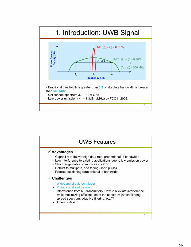
1. Introduction: UWB Signal
- Fractional bandwidth is greater than 0.2 or absolute bandwidth is greater than 500 MHz - Unlicensed spectrum 3.1 – 10.6 GHz - Low power emission ( < -41.3dBm/MHz) by FCC in 2002.
4
UWB Features
Advantages - Capability to deliver high data rate, proportional to bandwidth - Low interference to existing applications due to low emission power - Short range data communication (<10m) - Robust to multipath, and fading (short pulse) - Precise positioning (proportional to bandwidth)
- Wideband circuit techniques - Power constraint design - Interference from NB transmitters: How to alleviate interference
while maximizing efficient use of the spectrum (notch filtering, spread spectrum, adaptive filtering, etc.)?
- Antenna design
Challenges
3
5
Impulse radio UWB (IR-UWB) Uses extremely short pulses with duration on the order of
nanoseconds to transmit information
Advantages: - Low duty cycle of pulses, the transmitter power can be small - Carrier modulation is not required, no up and down conversion - No need of RF power amplifier - Simple architecture, low cost - Robust to multi-path fading
Disadvantages: - Difficult to generate and send extremely short pulses - Timing accuracy for short pulse reception, synchronization in the
receiver.
6
IR-UWB: Modulation
PPM
OOK
PAM
BPSK
Suitable for low data rate radio
4
7
UWB - Standard and Proposals
Time Hopped UWB (IEEE 802.15.4a Standard) - Old concept (radar) - Impulse Radio (IR-UWB has been chosen for PHY) - Low/moderate data rate
DS-CDMA UWB (IEEE 802.15.3a) - High data rate - UWB Forum supporting DS-UWB
Multi-Band OFDM UWB (IEEE802.15.3a) - High data rate - MBOA (MBO Alliance)
8
Applications of IR-UWB in WPAN - Short range wireless communication, home network
- Sensor networks (USN)
- Radar and Sensing: for Transportation, Police, Medical imaging.. Surveillance
- Tracking, localization like RF ID, TAG
5
9
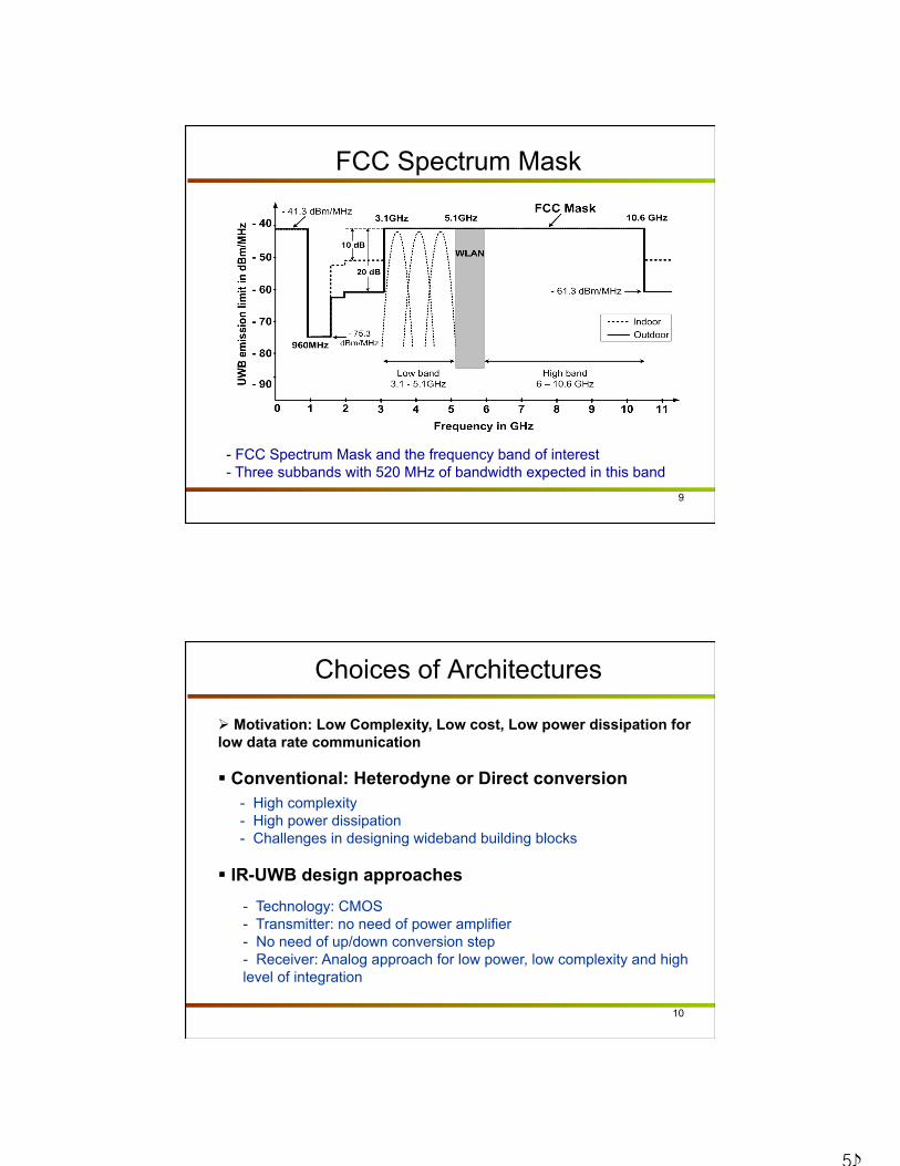
FCC Spectrum Mask
- FCC Spectrum Mask and the frequency band of interest - Three subbands with 520 MHz of bandwidth expected in this band
10
Choices of Architectures
Conventional: Heterodyne or Direct conversion - High complexity - High power dissipation - Challenges in designing wideband building blocks
IR-UWB design approaches - Technology: CMOS - Transmitter: no need of power amplifier - No need of up/down conversion step - Receiver: Analog approach for low power, low complexity and high level of integration
Motivation: Low Complexity, Low cost, Low power dissipation for low data rate communication
6
11
Receiver Architecture Consideration for IR-UWB
Coherent - Input signal distorted after antenna template signal not matched with incoming signal - Synchronization issue complex circuit
RAKE - Require number of fingers (bank of correlators) to gather signal power Non-Coherent + Energy Detection Pros: - OOK modulation, low complexity - Robust with clock jitter, - Relax distortion and phase non-linear requirement Cons: - Decision problem regarding determine optimal threshold - Simplicity vs Noise + Transmitted Reference (Autocorrelation) Pros: - 3dB better than ED Cons: - Required long and precise delay time (for integration time)
The FCC spectral mask to restrict the pulse power transmission
Requirement - Frequency range from 3.1 to 5.1GHz - Three bands, 520MHz wide each
Transmitter architecture
- Simplify architecture, only pulse generator without PA - Support OOK modulation
9
17
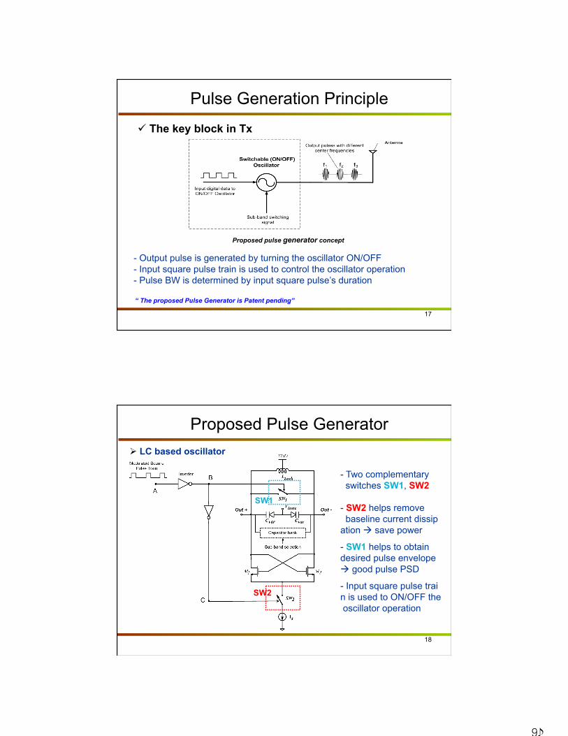
Pulse Generation Principle
- Output pulse is generated by turning the oscillator ON/OFF - Input square pulse train is used to control the oscillator operation - Pulse BW is determined by input square pulse’s duration
Proposed pulse generator concept
“ The proposed Pulse Generator is Patent pending”
The key block in Tx
18
Proposed Pulse Generator
- Two complementary switches SW1, SW2
- SW2 helps remove baseline current dissipation save power
- SW1 helps to obtain desired pulse envelope good pulse PSD
- Input square pulse train is used to ON/OFF the oscillator operation
LC based oscillator
SW2
SW1
10
19
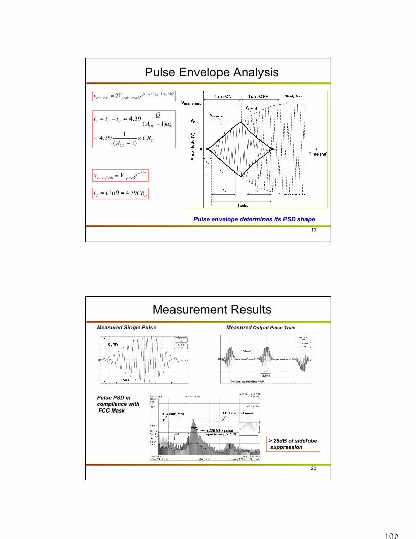
Pulse Envelope Analysis
Pulse envelope determines its PSD shape
20
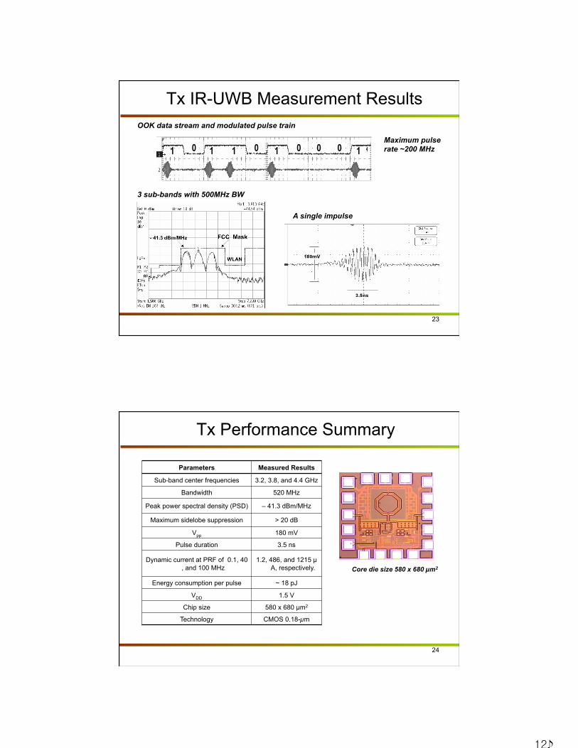
Measurement Results Measured Single Pulse
Pulse PSD in compliance with FCC Mask
Measured Output Pulse Train
> 25dB of sidelobe suppression
11
21
Performance Summary
Die size 560 µm x 550 µm
Tuan-Anh Phan, JeongSeon Lee, Vladimir Krizhanovskii, Le Quan, Seok-Kyun Han, and Sang-Gug Lee, "Energy-Efficient Low-Complexity CMOS Pulse Generator for Multiband UWB Impulse Radio," IEEE TCAS-I,2008
Feature - Ultra low power - No static DC current consumption - Low complexity, low cost - FCC compliant pulse - Large amount of sidelobe suppression - Suitable for multiband operation
22
Tx IR-UWB Design
Proposed transmitter with OOK modulation
Capacitor bank Added feature - OOK modulation - Band switching capability
12
23
Tx IR-UWB Measurement Results
3 sub-bands with 500MHz BW
OOK data stream and modulated pulse train
A single impulse
Maximum pulse rate ~200 MHz
24
Tx Performance Summary
Core die size 580 x 680 µm2
Parameters Measured Results
Sub-band center frequencies 3.2, 3.8, and 4.4 GHz
Bandwidth 520 MHz
Peak power spectral density (PSD) – 41.3 dBm/MHz
Maximum sidelobe suppression > 20 dB
Vpp 180 mV
Pulse duration 3.5 ns
Dynamic current at PRF of 0.1, 40, and 100 MHz
1.2, 486, and 1215 µA, respectively.
Energy consumption per pulse ~ 18 pJ
VDD 1.5 V
Chip size 580 x 680 µm2
Technology CMOS 0.18-µm
13
25
Transmitter Summary
Main Advantages: - Output pulse PSD compliant with FCC mask.
- No static current dissipation, only dynamic current which is proportional to PRF.
- Pulse center frequency can be changed, switchable for multi-band.
- Support OOK modulation.
- Simple circuit, very compact in size leading to low complexity low cost.
Tuan-Anh Phan, JeongSeon Lee, Vladimir Krizhanovskii, and Sang-Gug Lee, " A 18 pJ/pulse OOK CMOS Transmitter for Multiband UWB Impulse Radio," IEEE Microwave and Wireless Components Letter (MWCL), Sept. 2007.
26
C. Energy Detection IR-UWB Receiver
- Simplicity, low cost and low-power - Multiplier acts as Squarer for energy collection, no need of synchronization, avoid performance degradation due to timing jitter - Gating ON/OFF the whole Rx to reduced the baseline power dissipation - Able to recover the input data, acquisition based on Threshold estimation - Narrow band interference can be blocked using BPF - 1.5V supply in 0.18um CMOS, fully integrated with analog solution
14
27
IR-UWB LNA
UWB LNA Schematic
Wideband LNA is the most power hungry block in Rx
- LC filter combined with cascode topology lowest NF among wideband LNA design techniques - 1.5 Supply - Gating ON/OFF to reduce the baseline power consumption
28
IR-UWB LNA: Simulation
Band Width [GHz]
3 ~ 8
Max Gain [dB] 10.5
NF [dB] Min: 3.2 @ 4.9 GHz
Max: 3.9 @ 8 GHz
IIP3 [dBm] 0
Input matching (dB)
<-12
Static current / Supply [mA / V] 3.5 / 1.5
Continuous LNA S-parameter, NF performance
15
29
ON/OFF Transient - Clock is applied at the CG Transistor reduce settling time (5ns) - ON/OFF UWB LNA reserves wideband characteristic - Voltage gain is around 12 dB
Output
Input
Clock
Input and output transient of the ON/OFF UWB at PRF of 40MHz
Transient of one period
30
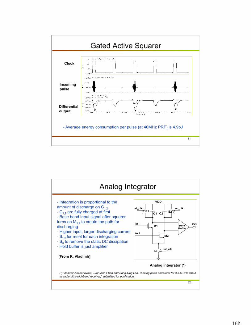
Gated Active Squarer
- Gilbert Cell based multiplier - Higher Gain - Gated current source No static power dissipation - Using square law
16
31
Gated Active Squarer
- Average energy consumption per pulse (at 40MHz PRF) is 4.9pJ
Clock
Incoming pulse
Differential output
32
Analog Integrator
Analog integrator (*)
(*) Vladimir Krizhanovskii, Tuan-Anh Phan and Sang-Gug Lee, “Analog pulse correlator for 3.5-5 GHz impulse radio ultra-wideband receiver,” submitted for publication.
- Integration is proportional to the amount of discharge on C1,2 - C1,2 are fully charged at first - Base band Input signal after squarer turns on M1,2 to create the path for discharging - Higher input, larger discharging current - S1,2 for reset for each integration - S3 to remove the static DC dissipation - Hold buffer is just amplifier
[From K. Vladimir]
17
33
Measurement Results
Measured output pulse trains of the Tx and Rx with the 100MHz OOK data pulse train at the input
Tuan-Anh Phan, Vladimir Krizhanovskii, and Sang-Gug Lee, “Low-Power CMOS Energy Detection Transceiver for UWB Impulse Radio System," IEEE Custom Integrated Circuits Conference (CICC' 07), San Jose, CA, USA, Sept 2007.
34
Comparator Block
- Dynamic latched comparator - No static power dissipation - Resolution: few 10mV - Extra Cap to remove the overshoot of clock
- Average power dissipation ~6.3pJ/pulse
Dynamic latched comparator
18
35
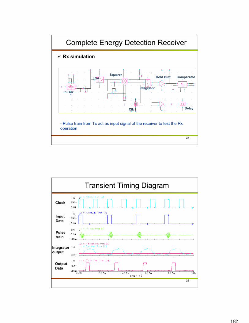
Complete Energy Detection Receiver
LNA Squarer
Integrator
Hold Buff
Clk
Pulser
Comparator
Delay
Rx simulation
- Pulse train from Tx act as input signal of the receiver to test the Rx operation
36
Transient Timing Diagram
Clock
Input Data
Pulse train
Integrator output
Output Data
19
37
Measurement Results: Transient
38
Measurement Results: NF and S11
- Average NF is around 13.5dB over the 3-5GHz band
- Measured receiver front-end NF
- S11 <-10 dB in 3-5 GHz range
- Measured receiver input matching S11
20
39
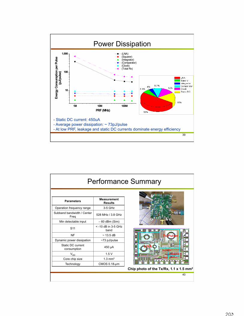
Power Dissipation
- Static DC current: 450uA - Average power dissipation: ~ 73pJ/pulse - At low PRF, leakage and static DC currents dominate energy efficiency
40
Performance Summary
Parameters Measurement Results
Operation frequency range 3-5 GHz
Subband bandwidth / Center Freq 528 MHz / 3.8 GHz
Min detectable input – 60 dBm (Sim)
S11 < -10 dB in 3-5 GHz band
NF ~ 13.5 dB
Dynamic power dissipation ~73 pJ/pulse
Static DC current consumption 450 µA
VDD 1.5 V
Core chip size 1.3 mm2
Technology CMOS 0.18-µm
Chip photo of the Tx/Rx, 1.1 x 1.5 mm2
21
41
Conclusions
A new pulse generation technique is proposed - Energy efficient, ultra low power, low complexity - Fully satisfy FCC spectral mask - Multiband operation
Energy Detection Receiver Architecture is best suited for low data rate (LDR) IR-UWB system - Low complexity, low power - No need accurate timing for synchronization - Relax accuracy requirement of pulse center frequency
Building blocks - Highly integrated using CMOS - Energy efficient design by removing static current dissipation
Feasible energy efficient, low cost IR-UWB transceiver
42
RF Design Consideration
Design and simulation - PVT and frequency shift are significant - Bond and pad models should be included - Separate analog and digital GND and VDD - Design with wide frequency tuning range - Confirmed with post-simulation is a must
Layout and PCB - Small devices and short signal path: reduce parasitic - Guard ring for different blocks: RF and digital - The less numbers of Pads, the higher chance of chip working
22
43
3. IR-UWB for Radar
Transceiver architecture of the UWB pulse radar.
Tx: - 540mV - 20dBr sidelobe rejection
Rx: - Coherent approach - Reduce misdetection due to jamming environment
44
Operation
Fig. 1. System clock timing.
Fig. 2. System with input and output transient simulation.
Anh Tuan Phan, Ronan Farrell, Min-suk Kang, Seok-Kyun Han, and Sang-Gug Lee, "Low-Power Sliding Correlation CMOS UWB Pulsed Radar Receiver for Motion Detection," IEEE International Symposium on Circuits and Systems (ISCAS' 09), Taipei, Taiwan, May 2009.
23
45
4. Future Plan
Research direction on IR-UWB
- Improve the performance like the sensitivity: more gain stages - Include the Antenna for design and test - Other approach for Tx (digital synthesized pulser) and Rx (other than non-coherent ED) - Design with other alternative approach, such as differential transmitted correlation receiver (DTR)
46
Differential Transmitted Reference (DTR)
Fig. 1: DTR UWB Receiver with an envelop detection scheme
Fig. 2: Fully Digital DTR UWB Receiver with an envelop detection scheme
- > Improve SNR and BER - > More accurate correlation, remove false alarm
At the Cost of more complex and high power dissipation
- Reduced freq, mismatch, relax ADC - Provide good correlation template - Avoid multipath signals