Page 1
The Pennsylvania State University
The Graduate School
College of Engineering
LOW POWER, SECURE AND ROBUST DESIGNS OF NON-VOLATILE
MEMORIES
A Dissertation in
Computer Science and Engineering
by
Seyedhamidreza Motaman
© 2018 Seyedhamidreza Motaman
Submitted in Partial Fulfillment
of the Requirements
for the Degree of
Doctor of Philosophy
December 2018
Page 2
ii
The dissertation of Seyedhamidreza Motaman was reviewed and approved* by the following:
Swaroop Ghosh
Assistant Professor of EE
Dissertation Advisor and Chair of Committee
Mahmut Kandemir
Professor of EECS
Saptarshi Das
Assistant Professor of ESM
Mehdi Kiani
Assistant Professor of EECS
Chitaranjan Das
Head of the Department of CSE
*Signatures are on file in the Graduate School
Page 3
iii
Abstract
In the last few decades, computation power has been increasing, thanks to CMOS scaling,
which in turn results in growing demand for high-density memories to meet the large bandwidth
requirement. However, CMOS scaling is approaching the end of roadmap and it is experiencing
significant challenges such as high power-density, process variation, high standby power, and
reliability issues. In addition, the increasing demand for high performance computing (HPC) and
integration of multiple cores on a single die have widened the speed gap between logic and memory,
that is known as the “memory-wall”. Process variability and standby power are posing severe
obstruction towards SRAM/DRAM scaling to future nodes. On one hand, industry and academia
began investigating alternative memory technologies, such as Spin-Torque Transfer RAM (STT-
RAM), Domain Wall memory (DWM), Phase-Change RAM (PCRAM), Ferro-electric RAM
(FeRAM), Resistive RAM (RRAM), and Magnetic RAM (MRAM). These emerging non-volatile
memory technologies offer the speed of SRAM, the high density of DRAM, and the non-volatility
of Flash memory. On the other hand, the speed gap between the processor and memory impedes
the continuous performance improvement of the traditional von Neumann architecture. In order to
address this challenge, extensive amount of research is performed to explore the alternative non-
von Neumann architectures based on the concept of computing in memory.
Among these memories, spintronic memories (i.e. STTRAM, DWM) have proven to be
potential alternatives to replace on-chip SRAM owing to their remarkable high density, zero
standby power, high speed, high endurance and CMOS compatibility. Nevertheless, STTRAM
suffers from crucial challenges such as high write energy, long write time and poor sense margin.
Furthermore, it suffers from process variation induced write latency and write power degradation.
Moreover, the sensitivity of magnets to ambient parameters and data persistence makes the
spintronic memories vulnerable to tampering and data leakage. In addition to the aforementioned
Page 4
iv
challenges associated with STTRAM, DWM suffers from shift latency and shift power overhead,
aspect ratio mismatch, and segregated read and write heads. The recent experimental studies have
revealed that RRAM is a promising alternative to implement main memory due to their small
footprint and zero standby power. Therefore, realizing logic operations within RRAM crossbar
arrays is a promising approach to implement computing-in-memory systems. However, RRAM
crossbar array suffers from sneak-path problem which leads to poor sense margin, higher power
consumption, and limited array size.
In the first part of this thesis, we propose the circuit and architectural techniques to
improve read yield, write latency, write power and data security of STTRAM. We introduce slope
sensing, a destructive sensing technique for elimination of the reference resistance variation in
order to enhance read yield of STTRAM arrays. Further, we propose a non-destructive sensing
scheme which exploits a voltage feedback and boosting (VFAB) approach to develop large sense
margin and substantially reduce sensing power. We introduce a novel and adaptive write current
boosting to mitigate process variation induced write latency and write power degradation. In this
technique, the bits experiencing worst-case write latency are fixed through write current boosting.
Next, we investigate data security of STTRAM last level cache under magnetic attack where we
apply low-overhead micro-architecture methods to avoid errors in presence of the magnetic attack.
In the second part of this thesis, we propose circuit and architectural techniques to
overcome the design challenges associated with DWM. We apply layout techniques such as sharing
of diffusion, bitlines and shift lines in order to enhance bitcell density. Circuit methods such as
merged read-write head for improvement of bitcell density and shift gating to reduce shift power
are proposed. Furthermore, we apply the micro-architecture techniques such as cache segregation
using a novel replacement policy as well as dynamic current boosting based on workload
monitoring in order to mitigate shift power and shift latency. Moreover, adaptive write and shift
Page 5
v
current boosting is proposed to mitigate process variation induced performance and power
degradation.
Lastly, we propose a low-power dynamic computing in memory system which can
implement various functions in the Sum of Product (SoP) form in RRAM crossbar array
architecture. This technique benefits from the nonlinear characteristic of a selector diode for
improvement of the sense margin in order to implement higher fan-in logic gates.
Page 6
vi
Table of Contents
List of Figures ........................................................................................................................... xi
List of Tables ............................................................................................................................. xviii
List of Abbreviations ................................................................................................................. xix
Acknowledgements ................................................................................................................... xxii
Chapter 1 ................................................................................................................................ 1
1. Introduction .................................................................................................................. 1 1.1. Contributions ..................................................................................................... 6
Chapter 2 ................................................................................................................................. 8
2. Introduction to Non-Volatile Memories ....................................................................... 8 2.1. Basics Principles of STTRAM .......................................................................... 9
2.1.1. Design Fundamentals of STTRAM ........................................................ 9 2.1.2. Modeling of STTRAM Switching Dynamics ......................................... 10 2.1.3. STTRAM Design Challenges ................................................................. 12
2.1.3.1. Tunneling Magnetoresistance (TMR) ....................................... 12 2.1.3.2. Oxide Breakdown ...................................................................... 12 2.1.3.3. Process Variation and Thermal Effects ..................................... 13 2.1.3.4. Sense Margin ............................................................................. 15
2.1.3.5. Read disturb ............................................................................... 15 2.1.3.6. Data Security ............................................................................. 15
2.2. Design Fundamentals of DWM ......................................................................... 17 2.2.1. Basics of DWM ...................................................................................... 17 2.2.2. Modeling of DWM ................................................................................. 18 2.2.3. DWM Challenges ................................................................................... 19
2.2.3.1. Shift Latency ............................................................................. 19 2.2.3.2. Segregated Read and Write Head .............................................. 19 2.2.3.3. Aspect Ratio Mismatch ............................................................. 20 2.2.3.4. Utilization Factor (UF) .............................................................. 20
2.3. Design Fundamentals of RRAM ....................................................................... 21 2.3.1. Basics of RRAM .................................................................................... 21 2.3.2. RRAM Design Challenges ..................................................................... 22
Chapter 3 ................................................................................................................................ 24
Page 7
vii
3. Robust and Low Power STTRAM Design ................................................................... 24 3.1. Introduction ....................................................................................................... 24 3.2. Improving Read Yield of STTRAM Array ....................................................... 26 3.2.1. Classification of Sensing Techniques ..................................................... 28 3.2.2. Background ............................................................................................ 29 3.2.2.1. Non-destructive Voltage Sensing Scheme [59] ......................... 29 3.2.2.1.1. Impact of process variation ................................................ 29 3.2.2.2. Destructive Self-reference Sensing Scheme [67] ...................... 32 3.2.2.2.1. Impact of process variation: .............................................. 34 3.2.3. Proposed Slope Sensing Technique ........................................................ 36 3.2.3.1. Slope Sensing Basic Operation.................................................. 37 3.2.3.2. Double Sampling ....................................................................... 39 3.2.3.3. Test Chip Implementation ......................................................... 40 3.2.3.3.1. Slope Sensing Circuit Design ........................................... 40 3.2.3.3.2. Impact of Process Variation ............................................. 42 3.2.3.3.3. Array Architecture ............................................................ 44 3.2.3.4. Test Results ............................................................................... 46 3.2.3.4.1. Conventional Sensing Test Results ................................. 46 3.2.3.4.2. Slope Sensing Test Results .............................................. 48 3.2.3.5. Applications .............................................................................. 51 3.2.4. VFAB: A Novel 2-Stage STTRAM Sensing Using Voltage
Feedback and Boosting .................................................................................... 52 3.2.4.1. Proposed VFAB Sensing Scheme ............................................ 52 3.2.4.1.1. Basic Operation ............................................................... 52 3.2.4.1.2. Simulation Results ........................................................... 54 3.2.4.2. Design Space Exploration ........................................................ 57 3.2.4.2.1. Design Method to Optimize Sense Margin ..................... 57 3.2.4.2.2. Impact of Discharge Time (td) ......................................... 57 3.2.4.2.3. Impact of Boost Capacitors and Boost Voltage............... 59 3.2.4.2.4. Impact of Boost Time (tb) ................................................ 62 3.2.4.2.5. Impact of TMR ................................................................ 62 3.2.4.2.6. Impact of Voltage Scaling ............................................... 63 3.2.4.3. Process, Temperature and Voltage Variation Analysis ............ 64 3.2.4.3.1. Monte Carlo Simulation Setup ........................................ 64 3.2.4.3.2. Read Yield ....................................................................... 65 3.2.4.3.3. Sense Amplifier OFFSET voltage Analysis .................... 66
3.2.4.3.4. Design Method for Process and Temperature
Variation Tolerance ....................................................................................... 67 3.2.4.3.5. Simulation Results ........................................................... 68 3.2.4.4. Comparison with other Sensing Schemes ................................. 71 3.2.4.5. Application ................................................................................ 73 3.3. Improving Write Performance of STTRAM ..................................................... 74 3.3.1. Related Works ........................................................................................ 75 3.3.2. Process Variation Analysis ..................................................................... 76 3.3.2.1. Process Variation in Write Operation ........................................ 76 3.3.2.2. Process Variation Tolerant Design ............................................ 79 3.3.3. Subarray Circuit Design ......................................................................... 79 3.3.3.1. Write Driver Design .................................................................. 79 3.3.3.2. Subarray Architecture ................................................................ 80
Page 8
viii
3.3.4. Cache Design for Adaptive Boosting ..................................................... 81 3.3.4.1. Methodology.............................................................................. 81 3.3.4.2. Cache Organization ................................................................... 82 3.3.4.3. Simulation Setup ....................................................................... 83 3.3.4.4. Simulation Results ..................................................................... 84 3.4. Summary ........................................................................................................... 86
Chapter 4 ................................................................................................................................ 88
4. Secure Design of STTRAM Last Level Cache ............................................................ 88 4.1. Introduction ....................................................................................................... 89 4.2. Related Work..................................................................................................... 92 4.3. Attack Models ................................................................................................... 93 4.3.1.1. Attack Model ....................................................................................... 93 4.3.1.2. Attack Sensing ..................................................................................... 94 4.4. Prevention Techniques ...................................................................................... 95 4.4.1. System Assumptions .............................................................................. 95 4.4.2. Preventive Solution: Stalling .................................................................. 97 4.4.3. Preventive Solution: Cache Bypass ........................................................ 98 4.4.4. Preventive Solution: Checkpointing ....................................................... 101 4.4.5. Checkpointing for Write-through Policy ................................................ 103 4.5. Simulation Results ............................................................................................. 104 4.6. Discussions ........................................................................................................ 107 4.6.1. Usage of Stalling, Bypassing and Checkpointing .................................. 107 4.6.2. Handling I/O Requests ........................................................................... 107 4.6.3. Ramping Attack Timing ......................................................................... 108 4.6.4. Continuous Attack .................................................................................. 108 4.7. Summary ........................................................................................................... 109
Chapter 5 ................................................................................................................................ 110
5. Robust, Low-Power and High Density Domain Wall Memories ................................. 110 5.1. Introduction ....................................................................................................... 110 5.2. Related Works ................................................................................................... 113 5.3. Bitcell Design .................................................................................................... 115 5.3.1. Merged Read-Write Head Design .......................................................... 115 5.3.2. Access transistor sizing .......................................................................... 117 5.3.3. Utilization Factor and Latency ............................................................... 118 5.3.3.1. Number/Positioning of merged head and UF ............................ 119 5.3.3.2. Latency ...................................................................................... 120 5.4. Bitcell Layout .................................................................................................... 121 5.4.1. Sharing of diffusion, bitlines and shift lines ........................................... 121 5.4.2. Process requirements for DWM integration ........................................... 123 5.5. Cache Design..................................................................................................... 124 5.5.1. Sub-Array design .................................................................................... 125 5.5.2. Cache Organization ................................................................................ 128 5.6. Cash Segregation and Workload Aware Current Boosting ............................... 129 5.6.1. Cache segregation ................................................................................... 129 5.6.2. Workload-aware current boosting .......................................................... 130
Page 9
ix
5.6.3. Simulation Setup and Result .................................................................. 134 5.7. Process Variation Analysis ................................................................................ 136 5.7.1. Process Variation in Write Head ............................................................ 136 5.7.2. Process Variation in Read Head ............................................................. 139 5.7.3. Process Variation Tolerant Design ......................................................... 139 5.7.4. Write Driver Design ............................................................................... 140 5.7.5. Shift Driver Design................................................................................. 142 5.7.6. Subarray Architecture ............................................................................. 143 5.8. Cache Design for Adaptive Boosting ................................................................ 143 5.8.1. Methodology .......................................................................................... 144 5.8.2. Cache Organization ................................................................................ 145 5.8.3. Simulation Setup and Result .................................................................. 145 5.9. Summary ........................................................................................................... 150
Chapter 6 ................................................................................................................................ 152
6. Dynamic Computing in Memory in Resistive Crossbar Arrays................................... 152 6.1. Introduction ...................................................................................................... 152 6.1. Background ....................................................................................................... 154 6.1.1. Basics of RRAM Crossbar Array ........................................................... 154 6.1.2. Static Computing in Memory (SCIM) Method ...................................... 158 6.1.3. Memristor Aided LoGIC (MAGIC) [137] .............................................. 160 6.2. Proposed Dynamic Computing in memory ....................................................... 161 6.2.1. Basic Operation ...................................................................................... 161 6.2.2. Impact of Gate Fan-in on Sense Margin ................................................. 165 6.2.3. Impact of Gate Fan-in on Power ............................................................ 167 6.3. Process and Temperature Variation Analysis ................................................... 168 6.3.1. Impact of Process and Temperature Variation on Sense Margin ........... 168 6.4. Implementation of Carry Select Adder using DCIM ........................................ 170 6.5. Evaluation and Comparison of different Computing in memory techniques .... 172 6.5.1. Power ...................................................................................................... 172 6.5.2. Latency ................................................................................................... 173 6.6. Summary ........................................................................................................... 174
Chapter 7 ................................................................................................................................ 175
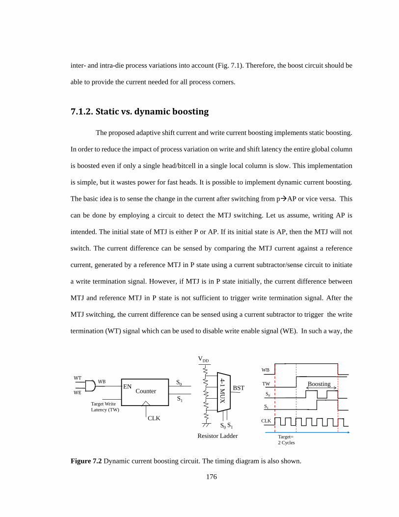
7. Future Work ................................................................................................................. 175 7.1. Improving write performance of Spintronic Memories ..................................... 175 7.1.1. Considerations for inter-die process variations ...................................... 175 7.1.2. Static vs. dynamic boosting .................................................................... 176 7.2. Security ............................................................................................................. 177 7.3. Computing in Memory ...................................................................................... 177
Chapter 8 ................................................................................................................................ 179
8. Summary ...................................................................................................................... 179
Appendix .................................................................................................................................. 182
Page 10
x
1. Referred Conferences ..................................................................................... 182 2. Referred Journals ............................................................................................ 183 3. Referred Patents ............................................................................................. 184
Bibliography .............................................................................................................................. 185
Page 11
xi
List of Figures
Figure 1.1 (a) Operating frequency scaling trend , and (b) On-chip cache size trend as
reported in [143-144]. ...................................................................................................... 1
Figure 1.2 (a) Percentage of area occupied by memory and logic, and (b) percentage of
dynamic and static power in scaled technologies (static power increases due to larger
on chip cache). ................................................................................................................. 3
Figure 2.1 (a) Schematic of a Spin Transfer Torque Random Access Memory (STTRAM);
and, (b) energy barrier separating the two MTJ magnetization states. ............................. 9
Figure 2.2 Simplified band diagram to demonstrate TMR effect in MTJ (a) parallel
magnetization (good band matching), and (b) anti-parallel magnetization (poor band
matching) of two magnetic layers. ................................................................................... 11
Figure 2.3 (a) Illustration of RH, RL and RREF distribution under process variation; and, (b)
write latency distribution for P→AP switching for two write currents. .......................... 14
Figure 2.4 Schematic of a conventional Domain Wall Memory. The MTJ at read and write
head and the overhead bits are also shown. ..................................................................... 16
Figure 2.5 (a) Schematic of the 1T1R structure of RRAM; (b) schematic of the 1D1R
structure of RRAM; and, (c) I-V curve of bipolar switching. ......................................... 20
Figure 2.6 Forming, SET and RESET switching mechanism in RRAM. ............................... 21
Figure 3.1 Taxonomy of STTRAM sensing schemes. ............................................................ 27
Figure 3.2 (a) Non-destructive sensing scheme; (b) Data0, reference and Data1 voltage
distributions. ..................................................................................................................... 30
Figure 3.3 SM0 and SM1 distribution for 10000 Monte-Carlo points; (a) original scheme
[59]; and, (b) with source degeneration [60]. ................................................................... 30
Page 12
xii
Figure 3.4 The impact of clamp voltage on sense margin for VClamp=0.7V and VClamp=0.9V.
.......................................................................................................................................... 31
Figure 3.5 (a) Self-reference sensing scheme; and, (b) sense circuit timing diagram is also
shown. .............................................................................................................................. 33
Figure 3.6 I-R characteristics of the two MTJs under process-variation. A variation in
resistance can change the sense margin. .......................................................................... 33
Figure 3.7 (a) V-I curves of an MTJ with high and low resistance states initially; and, (b)
optimum data current variation. ....................................................................................... 35
Figure 3.8 Sense margin distribution for 5000 Monte Carlo points. ....................................... 35
Figure 3.9 (a) Slope detection sense circuit; and, (b) simplified timing diagram. .................. 36
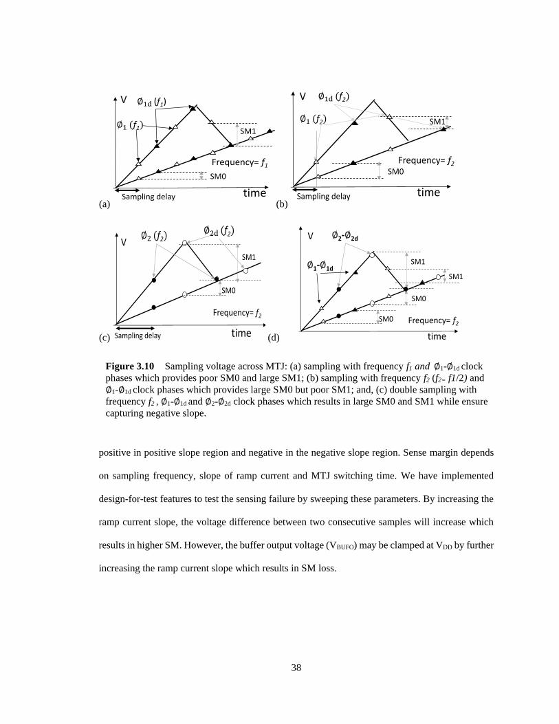
Figure 3.10 Sampling voltage across MTJ: (a) sampling with frequency f1 and ∅1-∅1d clock
phases which provides poor SM0 and large SM1; (b) sampling with frequency f2 (f2=
f1/2) and ∅1-∅1d clock phases which provides large SM0 but poor SM1; and, (c)
double sampling with frequency f2 , ∅1-∅1d and ∅2-∅2d clock phases which results in
large SM0 and SM1 while ensure capturing negative slope. ........................................... 38
Figure 3.11 Implementation details of slope detection sense circuit. ..................................... 40
Figure 3.12 Post layout simulation of slope sensing scheme along with timing diagram for
sense circuit-1(SC1) and SC2. ......................................................................................... 41
Figure 3.13 Low and high resistance distribution for 1000 points Monte Carlo simulation
for, (a) 5K-10K, and (b) 2.5K-5K. ................................................................................... 43
Figure 3.14 MTJ switching time distribution for 6uA/nS and 12uA/nS ramp current slopes
for 1000 Monte Carlo points. ........................................................................................... 43
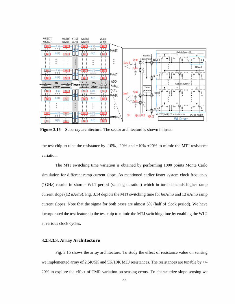
Figure 3.15 Subarray architecture. The sector architecture is shown in inset. ........................ 44
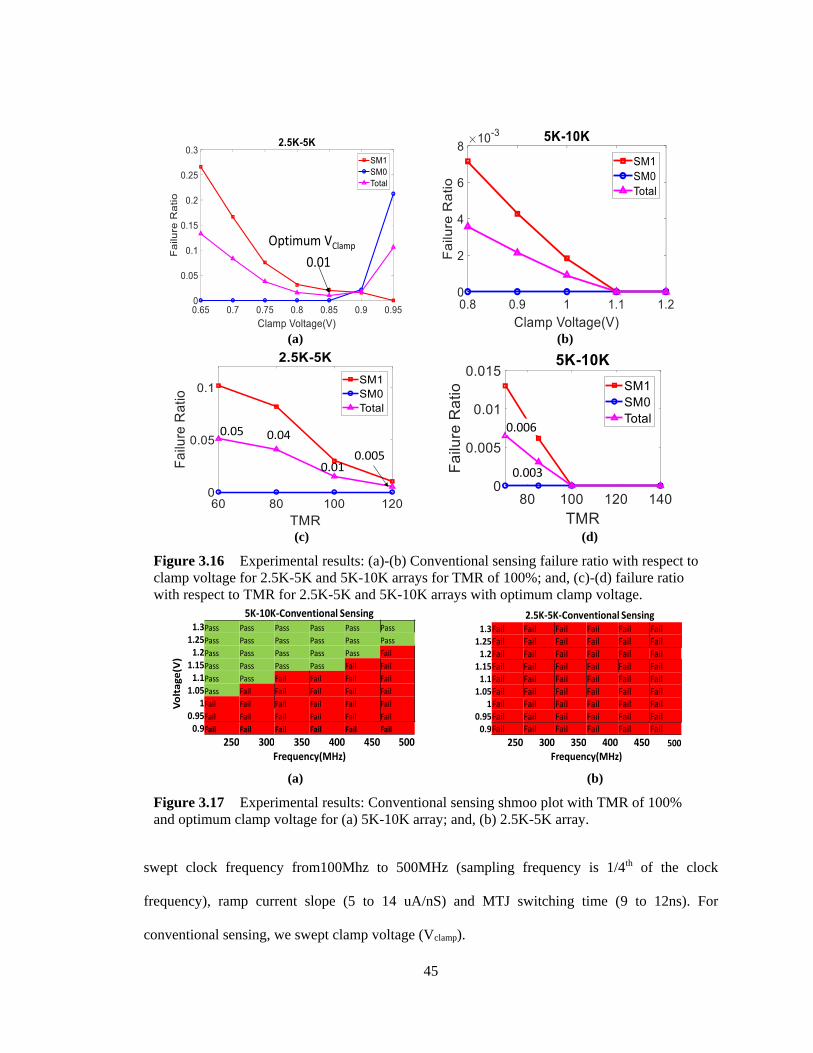
Figure 3.16 Experimental results: (a)-(b) Conventional sensing failure ratio with respect
to clamp voltage for 2.5K-5K and 5K-10K arrays for TMR of 100%; and, (c)-(d)
failure ratio with respect to TMR for 2.5K-5K and 5K-10K arrays with optimum
clamp voltage. .................................................................................................................. 45
Figure 3.17 Experimental results: Conventional sensing shmoo plot with TMR of 100%
and optimum clamp voltage for (a) 5K-10K array; and, (b) 2.5K-5K array. ................... 45
Figure 3.18 Oscilloscope capture of voltage across single-bitcell. Sensing starts by
activating WL1 and bitcell switches to low resistance state at the edge of WL2; and,
(b) the slope of voltage across bitcell for various current slope settings. Setting 00
indicatesthe lowest and 11 indicates the highest current slope. ....................................... 46
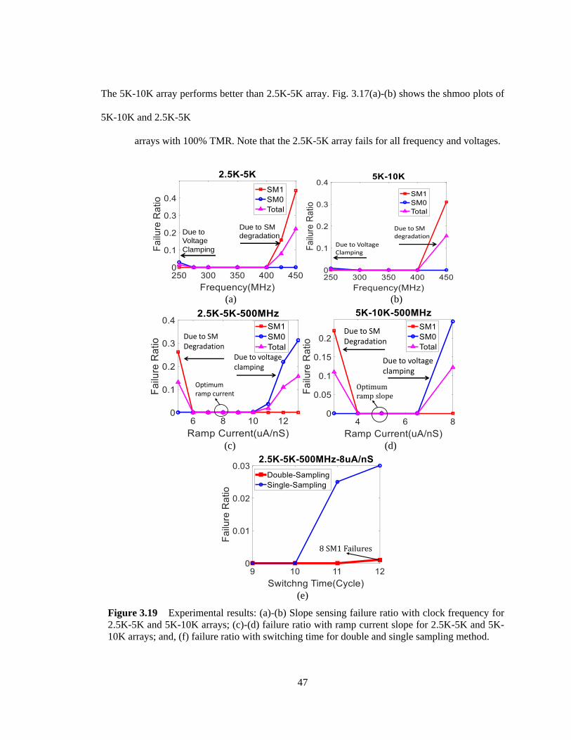
Figure 3.19 Experimental results: (a)-(b) Slope sensing failure ratio with clock frequency
for 2.5K-5K and 5K-10K arrays; (c)-(d) failure ratio with ramp current slope for 2.5K-
Page 13
xiii
5K and 5K-10K arrays; and, (f) failure ratio with switching time for double and single
sampling method. ............................................................................................................. 47
Figure 3.20 Experimental results: Slope sensing shmoo plot with TMR of 100% and
optimized ramp current slope and double sampling for, (a) 2.5K-10K array; and, (b)
5K-10K array. The # of failing chips out of 10 tested chips for failing voltage and
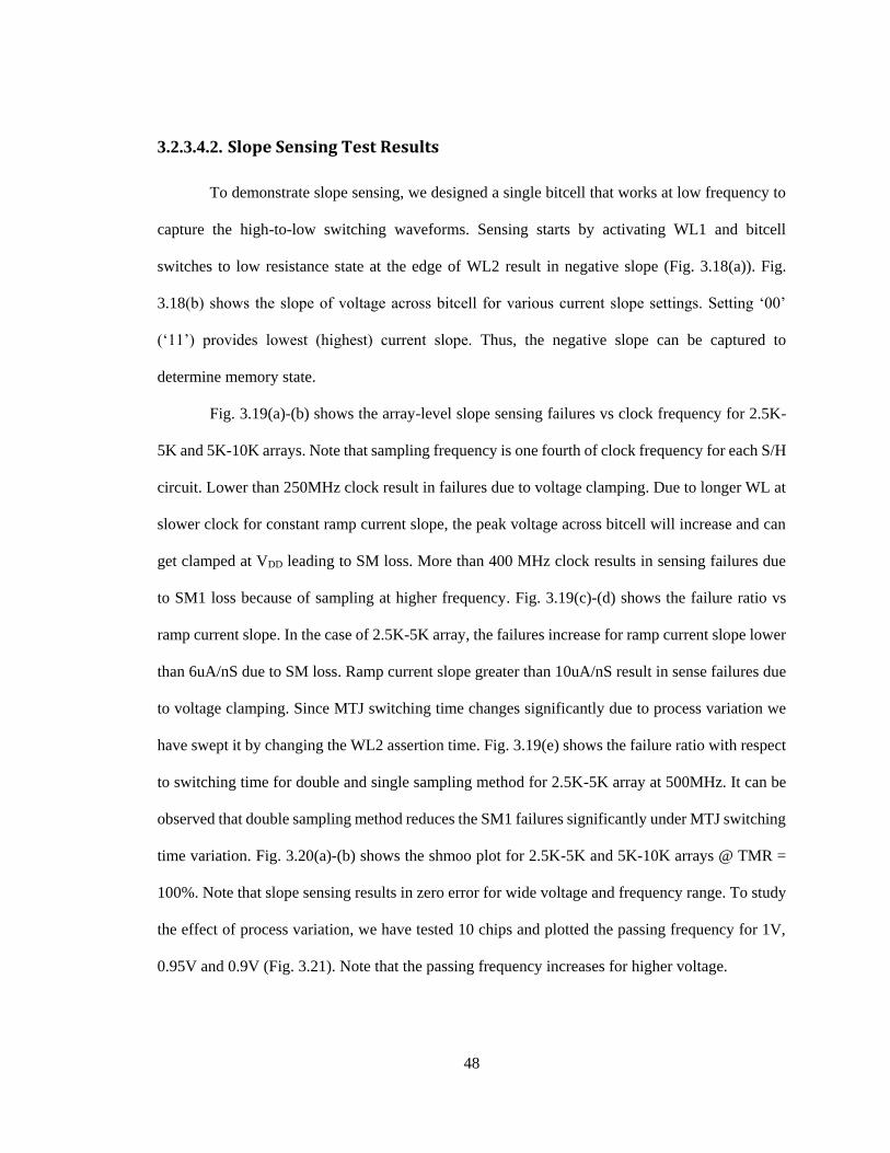
frequency is shown. .......................................................................................................... 49
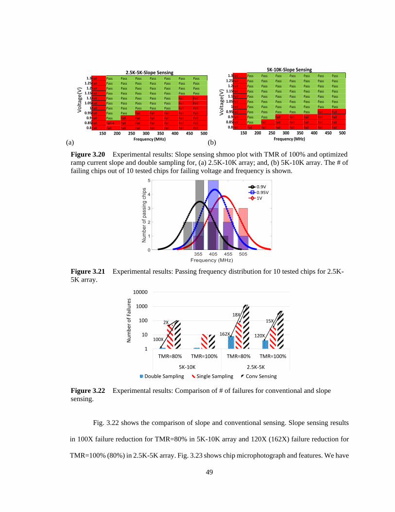
Figure 3.21 Experimental results: Passing frequency distribution for 10 tested chips for
2.5K-5K array. ................................................................................................................. 49
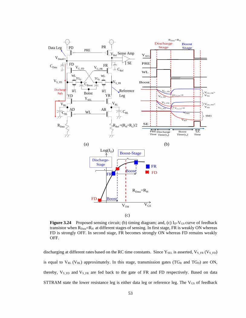
Figure 3.22 Experimental results: Comparison of # of failures for conventional and slope
sensing. ............................................................................................................................. 49
Figure 3.23 Chip microphotograph and features. .................................................................... 50
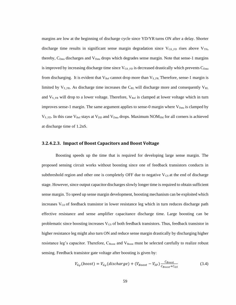
Figure 3.24 Proposed sensing circuit; (b) timing diagram; and, (c) ID-VGS curve of feedback
transistor when RData=RH at different stages of sensing. In first stage, FR is weakly
ON whereas FD is strongly OFF. In second stage, FR becomes strongly ON whereas
FD remains weakly OFF. ................................................................................................. 53
Figure 3.25 VRL, VBL and gate/source voltage of data feedback transistors (VG_FD and
VS_FD); and, (b) gate/source voltage of reference feedback transistor (VG_FR and
VS_FR) during discharge and boost stages where RData= RH ....................................... 55
Figure 3.26 Sense margin development during boosting stage. It can be noted that 800mV
sense-1 margin and 990mV sense-0 margin is developed using VFAB. ......................... 56
Figure 3.27 Impact of discharge time on feedback transistor VGS at the end of discharge
stage in TT, SS and FF corners; and, (b) impact of discharge time on sense margin
and VGS of feedback transistor after boosting when RData=RH. ......................................... 58
Figure 3.28 Impact of boost voltage on sense margin; and, (b) impact of CBoost on sense
margin for discharge time of 1.2nS. ................................................................................. 60
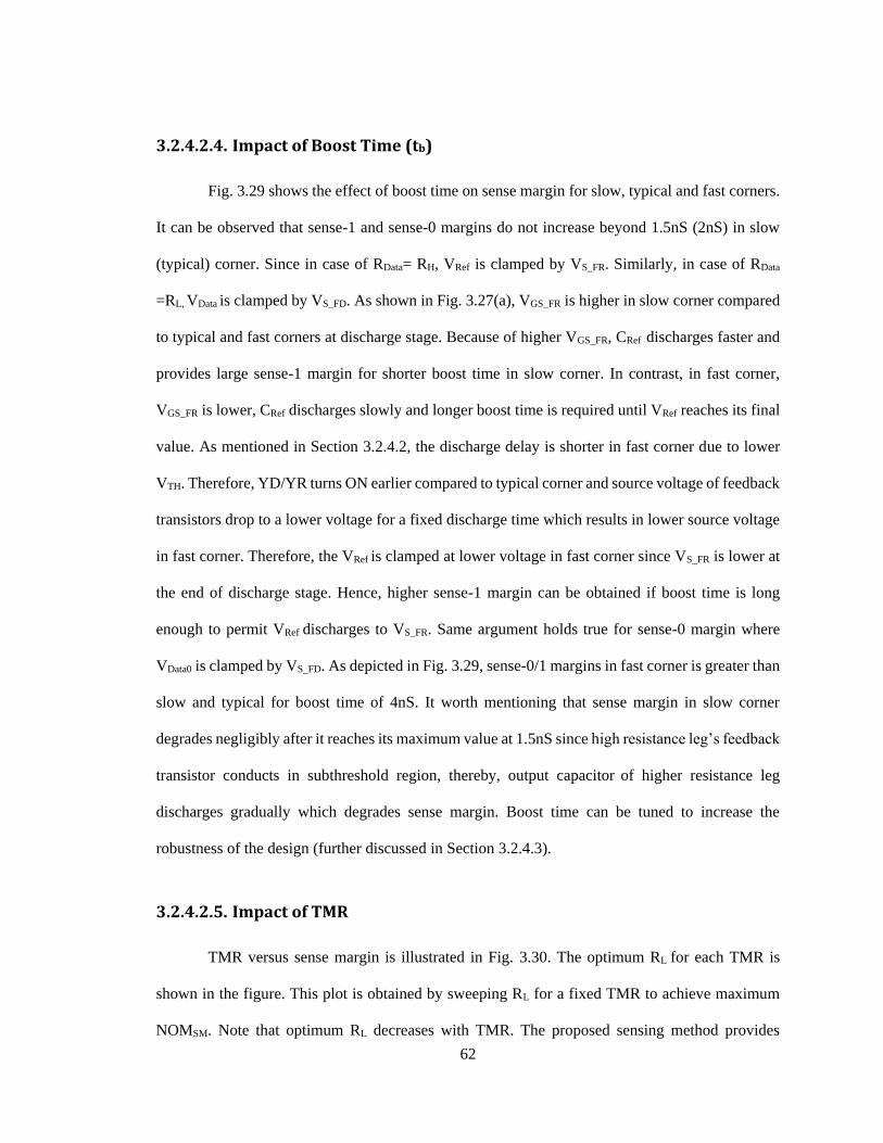
Figure 3.29 Impact of boost time on sense margin. ................................................................ 61
Figure 3.30 Fig. 8 Impact of TMR on sense margin (optimum RL is shown). ........................ 61
Figure 3.31 Impact of supply voltage variation on sense margin; and, (b) optimum sense
margin vs supply voltage; the optimum design parameters (VBoost, CBoost, td) are also
shown for each supply voltage. ........................................................................................ 63
Figure 3.32 Sense amplifier circuit; and, (b) SA offset voltage distribution for 1000 points
Monte-Carlo simulations. ................................................................................................. 66
Figure 3.33 (a) SM0 and, (b) SM1 distribution for 2000 Monte Carlo points (TT). The μ
and σ are also shown. ....................................................................................................... 69
Page 14
xiv
Figure 3.34 RAPY of top 4 design points which maximize PVTSM. The RAPY
improvement achieved by tuning VBST is also shown; (b) sensitivity of RAPY on
temperature in TT corner; and, (c) sensitivity of RAPY with respect to supply voltage
variation in TT, FF and SS corners. The WBST indicates the width of PMOS gate boost
capacitor. .......................................................................................................................... 70
Figure 3.35 (a) Various sources of variations in STTRAM bitcell and, (b) the proposed
methodology that involves modeling of tail of the distribution and adaptive boosting
to accelerate the tail. ......................................................................................................... 74
Figure 3.36 Write latency distribution for 5000 Monte Carlo points. The curve fitting to
model the tail is also shown; (b) write latency distribution using curve fitting model
for three different write currents. The worst case MTJ can be accelerated through high
write current. The 4 sigma delay is also shown. By boosting the current the number of
bits beyond 4 sigma delay can be reduced; and, (c) min, mean and max write latency
with write current. ............................................................................................................ 77
Figure 3.37 Boost enabled write and sense circuit; and (b) simulation results showing write
time improvement by enabling write boost. ..................................................................... 78
Figure 3.38 Subarray architecture showing boost enabled write and read circuit; and, (b)
cache organization and fuse bits. ..................................................................................... 80
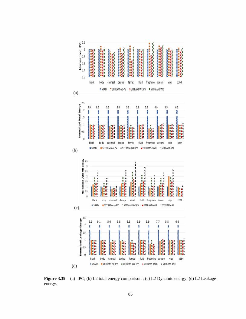
Figure 3.39 (a) IPC; (b) L2 total energy comparison ; (c) L2 Dynamic energy; (d) L2
Leakage energy. ............................................................................................................... 85
Figure 4.1 Two types of magnetic attacks: (a) gradually ramping attack; and, (b) sudden
attack. ............................................................................................................................... 91
Figure 4.2 Embedded attack sensor in memory array [40]. The details of sensor array with
peripheral circuits is shown in inset. Control logic is shared among the subarrays and
contains the logic to generate address, read, write and data and analyze the response. ... 94
Figure 4.3 Look aside cache architecture. ............................................................................... 96
Figure 4.4 (a) Control flow to activate/deactivate bypassing; and, (b) processing of read,
write requests during bypassing. ...................................................................................... 98
Figure 4.5 Bypassing of (a) read, and (b) write request with look-aside cache architecture.
.......................................................................................................................................... 100
Figure 4.6 Cache bypass architecture with checkpointing. ..................................................... 102
Figure 4.7 Control flow diagram of checkpointing. ................................................................ 102
Figure 4.8 Number of forced (FCP) and periodic checkpoints (PCP) for each PARSEC
benchmark. Periodic checkpointing is performed after every 2 million cycles. .............. 103
Page 15
xv
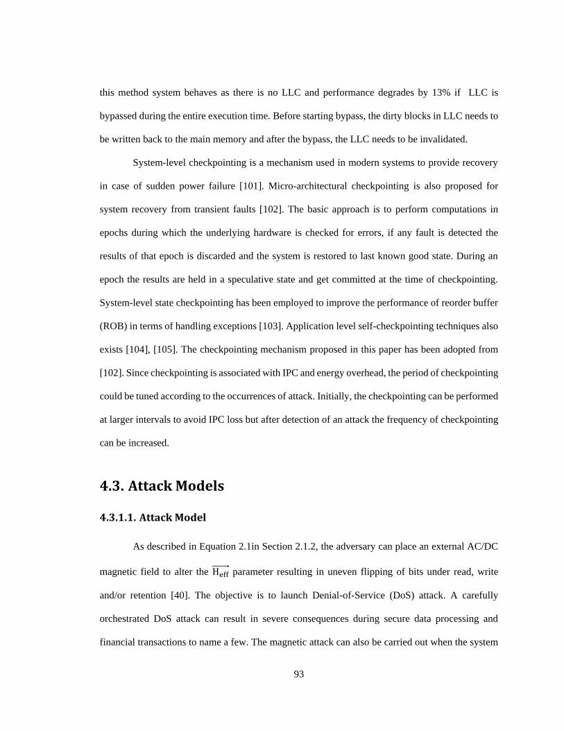
Figure 4.9 IPC results of baseline, bypassing and checkpointing with different attack rates
using; (a) SPLASH, and; (b) PARSEC benchmark suites. .............................................. 105
Figure 4.10 Energy results of baseline, bypassing and checkpointing with different attack
rates for SPLASH and PARSEC benchmarks: (a) total energy; and, (b) dynamic
energy ............................................................................................................................... 106
Figure 5.1 Synergistic system design proposed in this paper.................................................. 111
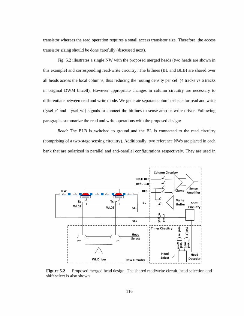
Figure 5.2 Proposed merged head design. The shared read/write circuit, head selection and
shift select is also shown. ................................................................................................. 116
Figure 5.3 Relationship between read current, write latency and access transistor size. ........ 118
Figure 5.4 UF vs number of Heads for NW with 40 bits. ....................................................... 119
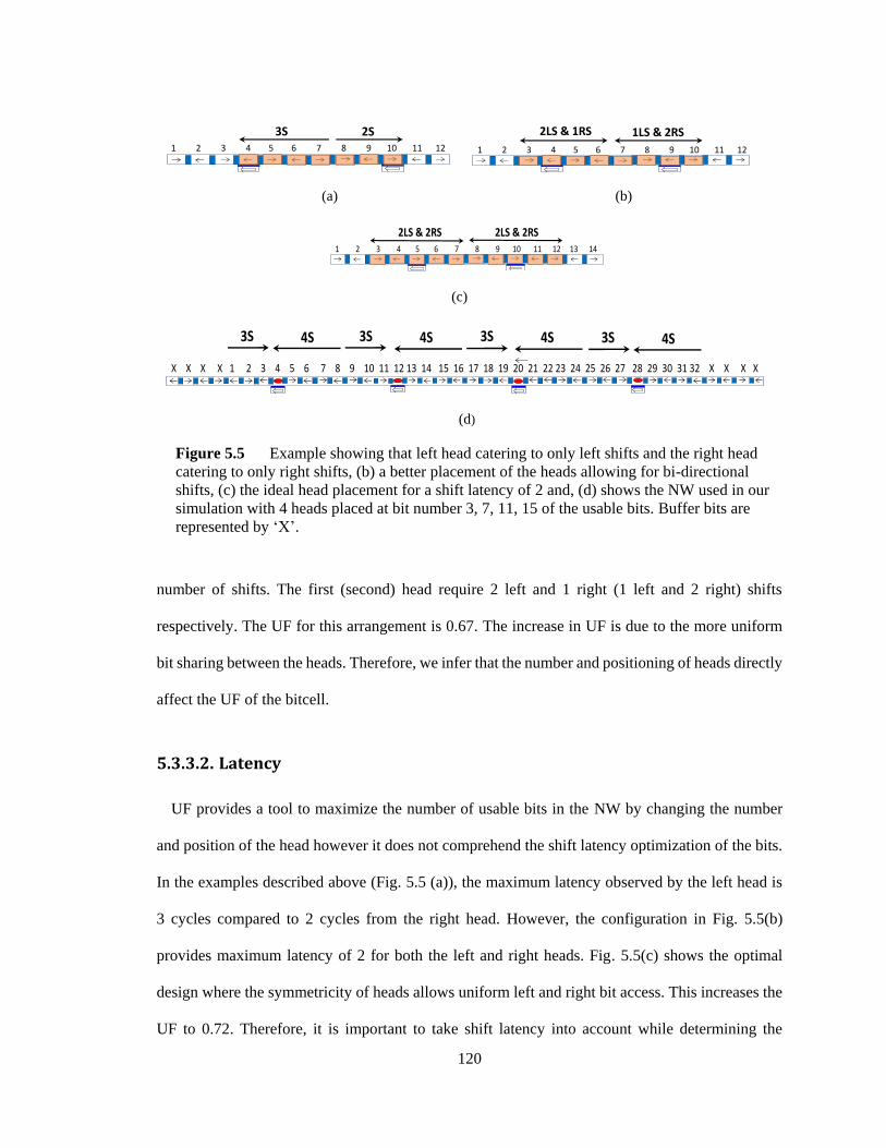
Figure 5.5 Example showing that left head catering to only left shifts and the right head
catering to only right shifts, (b) a better placement of the heads allowing for bi-
directional shifts, (c) the ideal head placement for a shift latency of 2 and, (d) shows
the NW used in our simulation with 4 heads placed at bit number 3, 7, 11, 15 of the
usable bits. Buffer bits are represented by ‘X’. ................................................................ 120
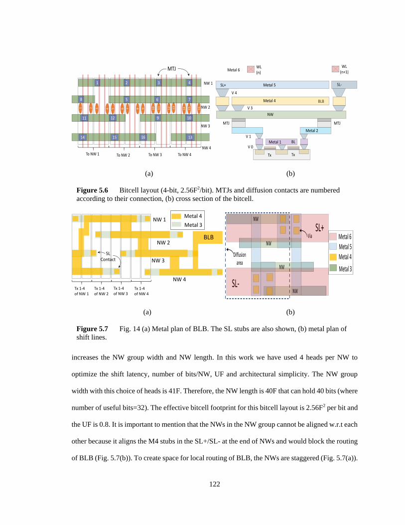
Figure 5.6 Bitcell layout (4-bit, 2.56F2/bit). MTJs and diffusion contacts are numbered
according to their connection, (b) cross section of the bitcell. ......................................... 122
Figure 5.7 Fig. 14 (a) Metal plan of BLB. The SL stubs are also shown, (b) metal plan of
shift lines. ......................................................................................................................... 122
Figure 5.8 Overview of proposed subarray with shift select, gating select and head selects.
WL strap is also shown. (b) Shift gating circuitry. .......................................................... 125
Figure 5.9 Write power versus write latency for three operating voltages. ............................ 126
Figure 5.10 (a) DW velocity vs input current using 1D model [41]. The DW velocity and
power of fast, medium and slow shift are indicated, (b) shift latency vs power. ............. 126
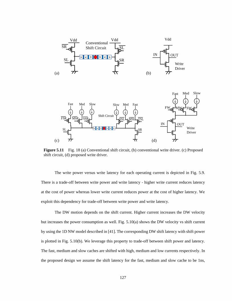
Figure 5.11 Fig. 18 (a) Conventional shift circuit, (b) conventional write driver. (c)
Proposed shift circuit, (d) proposed write driver. ............................................................. 127
Figure 5.12 Logical to physical mapping of a bank. Shaded ends of NW are buffer bits.
The set mapping on the NW is depicted. ......................................................................... 129
Figure 5.13 Proposed cache replacement policy. .................................................................... 129
Figure 5.14 Proposed segregated cache and replacement procedure in a Mat. ....................... 129
Figure 5.15 Fig. 23 Workload-aware write and shift current boosting. .................................. 131
Page 16
xvi
Figure 5.16 Number of L2 accesses for set1 & set2. Access profile for both 200K/500K
cycles are shown. ............................................................................................................. 131
Figure 5.17 Shift-current scaling of set2. ................................................................................ 132
Figure 5.18 Power and performance overhead for proposed workload-aware current
boosting. ........................................................................................................................... 132
Figure 5.19 Fig. 27 Performance comparison across different memory technologies. ........... 134
Figure 5.20 Fig. 28 Comparison of energy consumption of L2 cache across different
memory technologies. ...................................................................................................... 134
Figure 5.21 Performance comparison across different memory technologies for each
workload set. .................................................................................................................... 135
Figure 5.22 Energy comparison across different memory technologies for each workload
set. .................................................................................................................................... 135
Figure 5.23 Write latency distribution for 5000 Monte Carlo points. The curve fitting to
model the tail is also shown; (b) write latency distribution using curve fitting model
for three different write currents. The worst-case head can be accelerated through high
write current. The 4 sigma delay is also shown. By boosting the current the number of
bits beyond 4 sigma delay can be reduced; and, (c) min, mean and max write latency
with write current. ............................................................................................................ 137
Figure 5.24 Fig. 33 Effect of process variation on maximum write latency by considering
50% and 200% of original standard deviation of parameters reported in Table 3.1. ....... 138
Figure 5.25 Fig. 32 (a) Read latency distribution for 2000 Monte Carlo points. The curve
fitting to model the tail is also shown; (b) read latency distribution for 32M heads. ....... 139
Figure 5.26 Fig. 34 Mitigation of process variation on write latency by write and shift
current boosting. ............................................................................................................... 140
Figure 5.27 (a)& (b) Boost enabled write and shift driver; and (c) simulation results
showing write time improvement by enabling write boost. ............................................. 141
Figure 5.28 Subarray architecture showing boost enabled shift and write drivers, shift
gating for low power and head selection. ......................................................................... 142
Figure 5.29 Cache organization. ............................................................................................. 142
Figure 5.30 Shift current boosting for fast shifting. ................................................................ 145
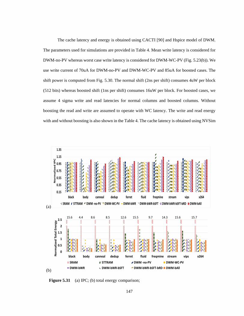
Figure 5.31 (a) IPC; (b) total energy comparison; .................................................................. 147
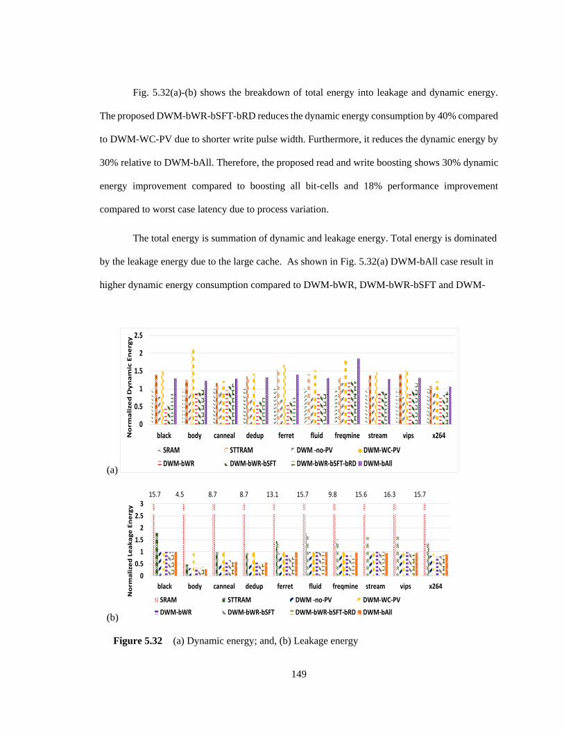
Figure 5.32 (a) Dynamic energy; and, (b) Leakage energy ..................................................... 149
Page 17
xvii
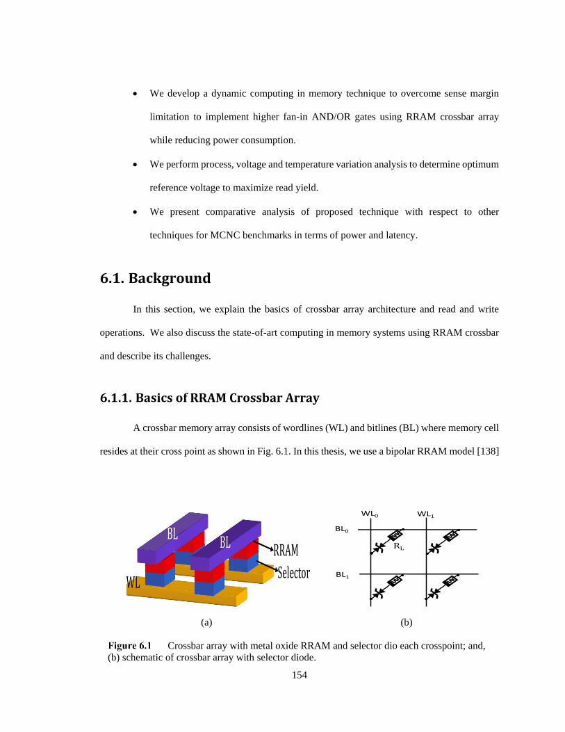
Crossbar array with metal oxide RRAM and selector dio each crosspoint; and,
(b) schematic of crossbar array with selector diode. ........................................................ 154
I-V curve RRAM model used in this study; (b) I-R characteristic of the RRAM
model; (c) I-V curve of selector diode used in this study; and, (d) the I-V characteristic
of bitcell composed of RRAM and selector diode. .......................................................... 155
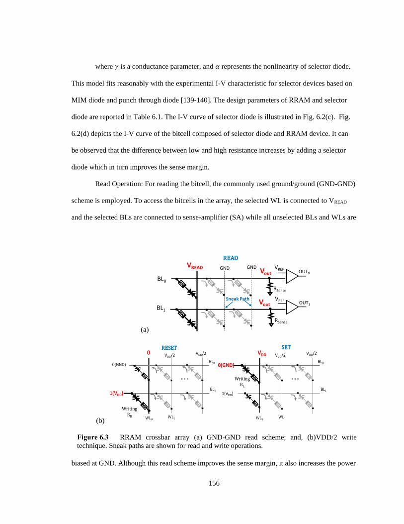
RRAM crossbar array (a) GND-GND read scheme; and, (b)VDD/2 write
technique. Sneak paths are shown for read and write operations. .................................... 156
Static computing in memory architecture in RRAM crossbar array. ..................... 158
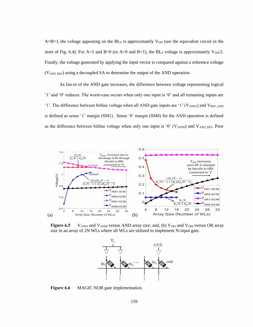
VAND1 and VAND0 versus AND array size; and, (b) VOR1 and VOR0 versus OR array
size in an array of 2N WLs where all WLs are utilized to implement N-input gate. ....... 159
MAGIC NOR gate implementation. ...................................................................... 159
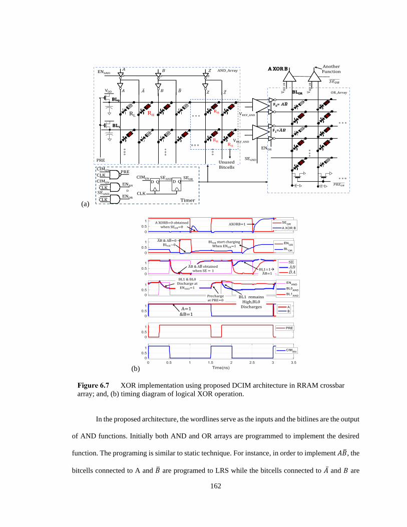
XOR implementation using proposed DCIM architecture in RRAM crossbar
array; and, (b) timing diagram of logical XOR operation. ............................................... 162
VAND,1,VAND,0 , VOR1 and VOR0 versus gate fan-in for, (a) conventional CIM in
array of 16 WLs, (b) DCIM in array of 64 WLs. ............................................................. 165
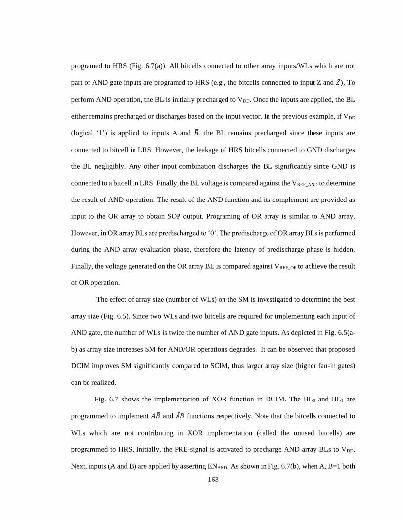
Power consumption versus number of inputs; (a) Dynamic CIM and, (b) static
CIM. ................................................................................................................................. 167
(a) VAND1 and VAND0 distribution for 1000 Monte-Carlo points @ -10oC and
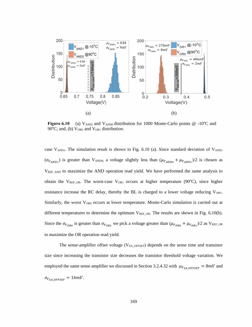
90oC; and, (b) VOR0 and VOR1 distribution. ...................................................................... 169
Implementation of 16-bit carry select adder using DCIM scheme. For sake of
brevity only low resistance connections are shown. ........................................................ 171
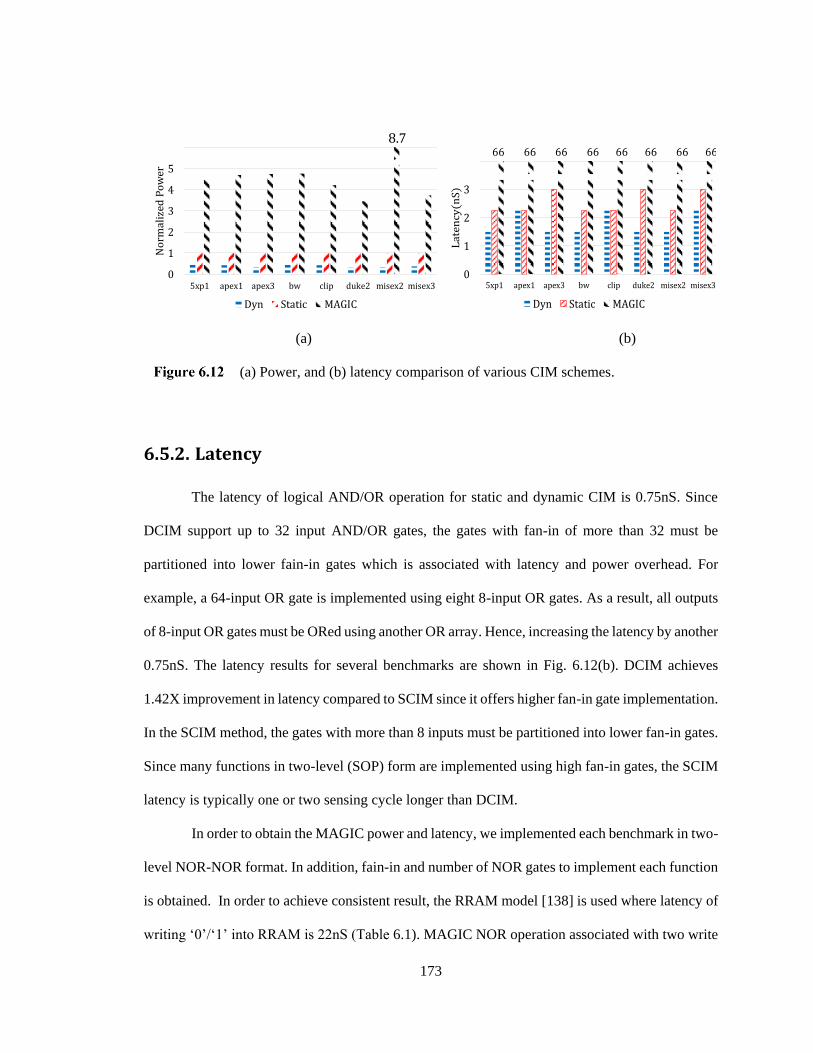
(a) Power, and (b) latency comparison of various CIM schemes. ....................... 173
Page 18
xviii
List of Tables
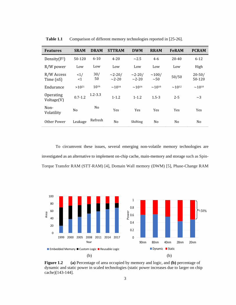
Table 1.1 Comparison of different memory technologies reported in [25-26]. ...................... 3
Table 2.1 MTJ parameters used. ............................................................................................. 10
Table 2.2 Magnetic constants used for DW dynamics. ........................................................... 18
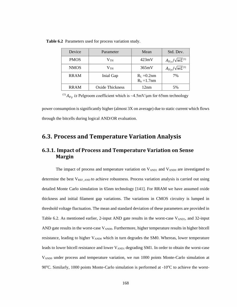
Table 3.1 Parameters used for process variation study. .......................................................... 29
Table 3.2 Comparison with other sensing schemes. ............................................................... 50
Table 3.3 Sense circuit parameters .......................................................................................... 57
Table 3.4 Parameters used for process variation study. .......................................................... 64
Table 3.5 Comparison with conventional voltage sensing scheme. ........................................ 72
Table 3.6 Comparison with other sensing scheme. ................................................................. 72
Table 3.7 Processor Configuration .......................................................................................... 81
Table 3.8 Design parameters for different cache configurations (22nm Technology). ........... 83
Table 5.1 Processor configuration. .......................................................................................... 133
Table 5.2 Design parameters for different cache configurations (22 nm technology). ........... 136
Table 6.1 List of design parameters. ....................................................................................... 157
Table 6.2 Parameters used for process variation study. ......................................................... 168
Table 6.3 Comparison of 16-bits adder implementation using different CIM schemes. ......... 170
Page 19
xix
List of Abbreviations
ADC Analog to Digital Converter
AP Anti-Parallel
BCT Block Counter
BL Bit Line
DIBL Drain Induced Barrier Lowering
DAC Digital to Analog Converter
DRAM Dynamic Random Access Memory
DCIM Dynamic Computing in Memory
DMA Direct Memory Access device
DoS Denial of Service
DW Domain Walls
DWM Domain Wall Memory
ECC Error Correction Code
EWT Early Write Termination
eDRAM embedded DRAMs
FeFET Ferroelectric FET
FeRAM Ferroelectric RAM
FF Flip-flop
FL Free Layer
GIDL Gate Induced Drain Leakage
GBDP Grouping-Based Data Placement
HRS High Resistance State
Page 20
xx
HPC High Performance Computing
IC Integrated Circuit
IMA In-plane Magnetic Anisotropy
IoT Internet of Things
IPC the instruction per cycle
LLG Landau-Lifshitz-Gilbert
LLC Last Level Cache
LS Left-Shift (LS)
LRS Low Resistance state
MAGIC Memristor Aided LoGIC
MIM Metal-Insulator-Metal
MRAM Magnetic RAM
MTJ Magnetic Tunnel Junction
MRU most recently used
NBTI Negative Bias temperature Instability
NVM Non-Volatile Memory
NW Nanowire
PCM Phase Change Memory
P Parallel
PCP Periodic Checkpointing
PC program counter
PMA Perpendicular Magnetic Anisotropy
PL Pinned Layer
PUF Physically Unclonable Function
RAPY Read Access Pass Yield
RDPY Read Disturbance Pass Yield
RS Right-Shift
RH High Resistances
Page 21
xxi
RO Ring Oscillator
RRAM Resistive RAM
Sa Sense Amplifier
SCIM Static Computing in Memory
SE Sense Enable
SHE Spin Hall Effect
SL Source Line
SM Sense Margin
SM0 Sense-0 Margin
SOP Sum of Product
SRAM Static Random-Access Memory
STTRAM Spin Transfer Torque RAM
TDDB Time Dependent Dielectric Breakdown
TMR Tunneling Magnetoresistance
TRNG True Random Number Generator
UF Utilization Factor
VFAB Voltage Feedback And Boosting
WL Wordline
Page 22
xxii
Acknowledgements
I would like to thank a few people who helped me in this journey. Firstly, I would like to express
my sincere gratitude to my advisor Prof. Swaroop Ghosh, for his continuous guidance,
patience, enthusiasm and support throughout my doctoral studies. He was always very welcoming
to answer my questions and helping me in all the time of research. Dr Ghosh’s insight and advice
on both research and my career are invaluable.
I would like to thank Dr. Jaideep Kulkarni provided me insight into the industry and
offered a practical perspective to my research direction. Collaborating with him on couple of
publications helped me understand the industry challenges in designing non-volatile memories. I
would also like to thank the committee members for their help and guidance during my PhD.
I thank my fellow labmates for the motivating discussions, for the sleepless nights we
were working together before deadlines, and for all the fun we have had in the last four years. I
would like to thank Jae, Asmit, Nasim, Saki, Rekha and Anirudh for their continued support,
motivation, and encouragement.
This material is based on work supported by the Semiconductor Research Corporation
(SRC) under award number (#2727.001), the National Science Foundation (NSF) under award
numbers (#CNS-1722557, #CCF-1718474, DGE-1723687 and DGE-1821766), and the Defense
Advanced Research Projects Agency (DARPA) Young Faculty Award under award number
(#D15AP00089).
Any opinion, findings, and conclusions or recommendations expressed in this publication
are those of the authors and do not necessarily reflect the views of the Semiconductor Research
Corporation, National Science Foundation and Defense Advanced Research Projects Agency.
Page 23
xxiii
To my family
Page 24
1
Chapter 1
1. Introduction
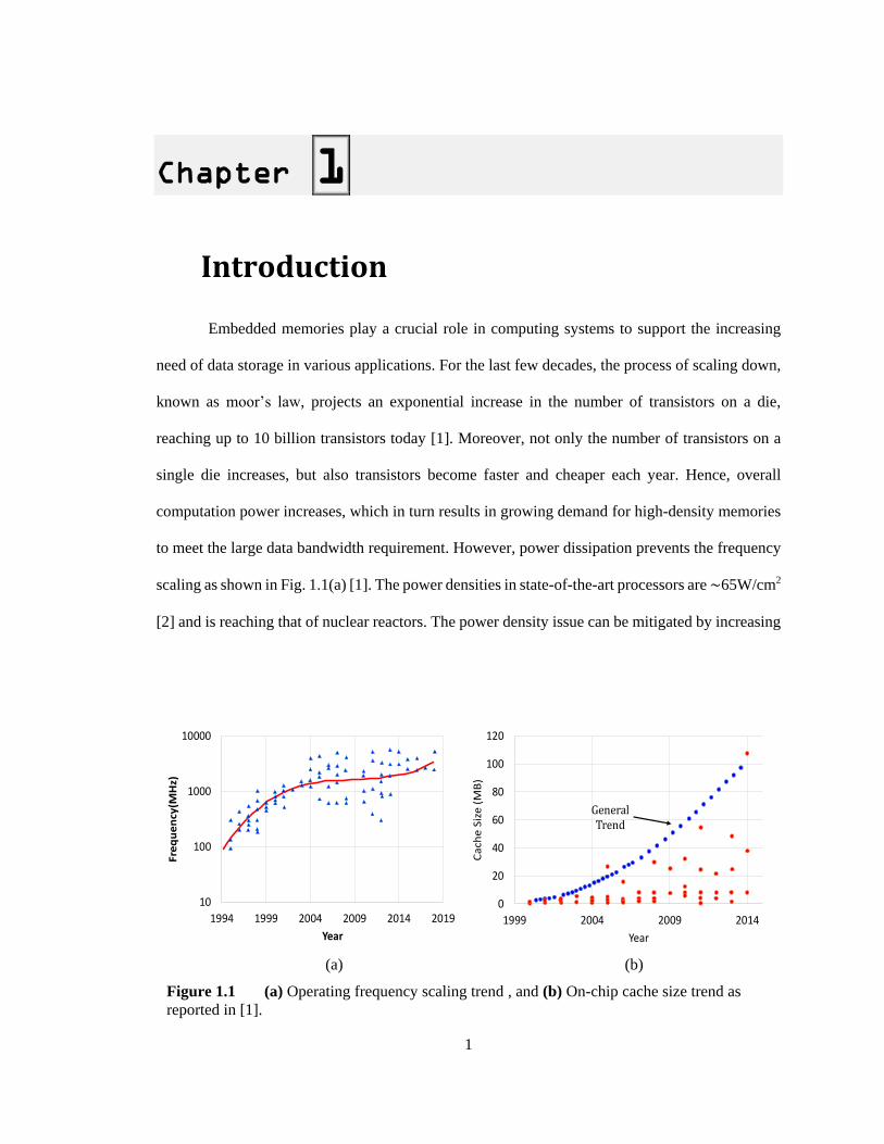
Embedded memories play a crucial role in computing systems to support the increasing
need of data storage in various applications. For the last few decades, the process of scaling down,
known as moor’s law, projects an exponential increase in the number of transistors on a die,
reaching up to 10 billion transistors today [1]. Moreover, not only the number of transistors on a
single die increases, but also transistors become faster and cheaper each year. Hence, overall
computation power increases, which in turn results in growing demand for high-density memories
to meet the large data bandwidth requirement. However, power dissipation prevents the frequency
scaling as shown in Fig. 1.1(a) [1]. The power densities in state-of-the-art processors are ∼65W/cm2
[2] and is reaching that of nuclear reactors. The power density issue can be mitigated by increasing
(a) (b)
Figure 1.1 (a) Operating frequency scaling trend , and (b) On-chip cache size trend as
reported in [1].
10
100
1000
10000
1994 1999 2004 2009 2014 2019
Fre
qu
en
cy(M
Hz)
Year
0
20
40
60
80
100
120
1999 2004 2009 2014
Ca
che
Siz
e (
MB
)
Year
General Trend
Page 25
2
the number of processor cores which in turn requires larger on-chip cache to take full advantage of
multi-core systems. As shown in Fig. 1.1(b), the capacity of on-chip memory increases every year.
Fig.1.2 (a) shows that as technology scales, more and more of on-chip area is dedicated to memory.
So far, CMOS scaling allows smaller transistor size to increase the capacity of on-chip caches.
However, Moore’s law predicts exponential scaling and will not continue indefinitely because of
numerous technological challenges [3], such as precision in photo lithographic process, and
electrical limitations due to short channel effects. Furthermore, the CMOS scaling is associated
with challenges such as increased subthreshold leakage due to Drain Induced Barrier Lowering
(DIBL), Gate Induced Drain Leakage (GIDL), Hot Carrier Injection (HCI), Time Dependent
Dielectric Breakdown (TDDB), Negative Bias Temperature Instability (NBTI), high power
density, velocity saturation due to mobility degradation, and process variations.
In the last few years, the increasing demand for high performance computing (HPC) and
integration of multiple cores on a single die have increased the speed gap between logic and
memory, the so-called “memory-wall”. Conventional CMOS memories i.e., Static Random Access
Memory (SRAM) and Dynamic Random Access Memory (DRAM) have been the popular choices
to build on-chip caches and main memory for the last several decades. However, SRAM and
DRAM seem to be approaching a brick wall. SRAM and DRAM are volatile memories meaning
that they require a constant power supply to retain the state. SRAM cell drastically consumes static
(leakage) power, and DRAM cell requires a periodical refresh. On one hand, process variability
and standby power are posing severe obstruction towards SRAM/DRAM scaling to future nodes.
Fig. 1.2(b) shows that the leakage power is exceeding dynamic power in scaled technology. On the
other hand, emerging energy-constrained and bandwidth hungry electronic gadgets demand for
larger on-chip cache which cannot be satisfied with SRAM. Thus, the memory hierarchy design
must substantially scale in performance, power, and density to sustain the processing demands of
next-generation applications.
Page 26
3
To circumvent these issues, several emerging non-volatile memory technologies are
investigated as an alternative to implement on-chip cache, main-memory and storage such as Spin-
Torque Transfer RAM (STT-RAM) [4], Domain Wall memory (DWM) [5], Phase-Change RAM
(b) (b)
Figure 1.2 (a) Percentage of area occupied by memory and logic, and (b) percentage of
dynamic and static power in scaled technologies (static power increases due to larger on chip
cache)[143-144].
0
20
40
60
80
100
1999 2000 2005 2008 2011 2014 2017
Are
a
Year
Embedded Memory Custom Logic Reusable Logic
~50%
0
0.2
0.4
0.6
0.8
1
1.2
90nm 80nm 40nm 28nm 20nm
Po
we
r
Dynamic Static
Table 1.1 Comparison of different memory technologies reported in [25-26].
Features SRAM DRAM STTRAM DWM RRAM FeRAM PCRAM
Density(F2) 50-120 6-10 4-20 ~2.5 4-6 20-40 6-12
R/W power Low Low Low Low Low Low High
R/W Access Time (nS)
<1/ <1
30/ 50
~2-20/ ~2-20
~2-20/ ~2-20
~100/ ~50
50/50 20-50/ 50-120
Endurance >1021 1016 ~1016 ~1016 ~1010 ~1012 ~1010
Operating Voltage(V)
0.7-1.2 1.2-3.3
1-1.2 1-1.2 1.5-3 2-5 ~3
Non-Volatility
No No
Yes Yes Yes Yes Yes
Other Power Leakage Refresh No Shifting No No No
Page 27
4
(PCRAM) [6-7], Ferro-electric RAM (FeRAM) [8], Resistive RAM (RRAM)) [9], and Magnetic
RAM (MRAM) [10] that are explored as potential alternatives to existing memories. These
emerging NVM technologies offer the speed of SRAM, high density of DRAM, and the non-
volatility of Flash memory.
Table 1.1 compares memory technologies in terms of density, access time, and endurance.
Among these memory technologies, spintronic memories (i.e. STTRAM, DWM) have proven to
be potential alternatives to replace on-chip SRAM. These memory technologies offer high-density,
zero standby power, high speed, high endurance and CMOS compatibility. STTRAM provides
small footprint of ~4-20F2, extremely good endurance of > 1016 and read/write access time of 2-
20ns. DWM provides small footprint as low as 2.5F2 [11] and similar endurance. Even though
read/write access time of DWM is longer due to shift-based access mechanism, very small footprint
makes it a promising candidate to implement large on-chip caches. From an industrial standpoint,
HP and Hynix are planning to replace flash memory and later DRAM/SRAM with RRAM.
Furthermore, Toshiba is planning to implement 512KB STTRAM L2 cache to save power [12].
Everspin released commercialized samples of 64MB STT-RAM [13].
On the other hand, the speed gap between the processor and memory impedes the
continuous performance improvement of the traditional von Neumann architecture. To address this
challenge, extensive amount of research has been conducted to explore alternative non-von
Neumann architectures based on the concept of computing in memory. Von Neumann computing
separates memory and processing elements leading to performance and energy bottlenecks due to
frequent data transfers. With conventional von Neumann computing struggling to implement high
performance and energy-efficient computing systems, there is a pressing need to explore alternative
computing models. CMOS switches, although universal, fails to offer additional features to meet
this end goal. Recent experimental studies have revealed that RRAM is a promising alternative to
implement main memory due to small footprint and zero standby power. Therefore, realizing logic
Page 28
5
operations within RRAM crossbar arrays is a promising approach to implement computing in
memory systems. Resistive crossbar arrays possess many promising features that can not only
enable high-density and low-power storage but also non-von Neumann compute models. Various
computing in memory schemes have been proposed to implement dot products in RRAM crossbar
array. Digital to analog converter (DAC) and analog to digital converter (ADC) are required as
peripheral circuitry to implement dot product in RRAM crossbar array. These architectures can
implement matrix multiplication [14] and various computing paradigms such as neuromorphic
computing [15-16] and approximate computing [17]. Spintronic devices are also investigated for
ultra-low power computing based on artificial neural network. Interestingly, variety of new
structures have been proposed to suit particular application e.g., full adders [18], MTJ neurons [19-
21] and MTJ synapses [22-24]. Two basic operations in artificial neural network are weighted
summation of inputs and thresholding operation. MTJ switching basically behaves as a current
thresholding device. Thus, MTJ can be exploited to implement thresholding operation of a neuron
in a memristive crossbar array. However, due to small resistance difference between two states of
MTJ, STT synapse cannot compete with that of RRAM to implement weighted summation.
Despite all the advantages, spintronic memories suffer from high write energy, long write
time, poor sense margin (SM), read disturb and reliability issues such as oxide break down.
Furthermore, they bring new data security issues that were absent in volatile memory counterparts
such as SRAM. The free layer of MTJ can flip under the influence of external magnetic field that
can be exploited by the adversary. In this dissertation, we explore circuit and architectural
techniques to address spintronic memories design challenges. In addition, we investigate RRAM
crossbar array to implement energy-efficient computing in memory paradigm.
Page 29
6
1.1. Contributions
In this dissertation, we have explored STTRAM, DWM and RRAM as alternatives to
CMOS to implement memory and computing systems. First, we describe the basic principles of
these memories and their design challenges.
In the third chapter, we propose circuit and architectural techniques to improve read yield
and write performance of STTRAM which is summarized as follows:
• Due to poor TMR, the voltage/current differential between low and high resistance states of
STTRAM decreases which degrades the SM. Furthermore, process variation reduces this
difference even further resulting in a poor sense margin. In this chapter we propose, slope
sensing, a destructive sensing technique to eliminate reference resistance variation to
enhance the read yield of STTRAM arrays. Additionally, we introduce a non-destructive
sensing scheme that exploits a voltage feedback and boosting (VFAB) technique to develop
large sense margin. Moreover, this method reduces the sensing power significantly by
eliminating static current.
• Process variation along with stochastic nature of MTJ switching results in a large spread in
the write latency variation. We propose a novel and adaptive write current boosting to
address this issue. In this technique, the bits experiencing worst-case write latency are fixed
through write current boosting.
In the fourth chapter, we investigate the data security of STTRAM last level cache under magnetic
attack. We apply low-overhead micro-architecture techniques to avoid errors in presence of
magnetic attack which include:
• Stalling where the system is halted during attack.
• Cache bypass during gradually ramping attack where the last level cache (LLC) is bypassed
and the upper level caches interact directly with the main memory.
Page 30
7
• Checkpointing along with bypass during sudden attack where the processor states are saved
periodically, and the LLC is written back at regular intervals. During attack, the system goes
back to the last checkpoint and the computation continues with bypassed cache.
In the fifth chapter, we propose circuit and architectural techniques to address the DWM design
challenges as follows:
• At the circuit level, we introduce merged read-write head to increase bitcell density by
merging the segregated read and write access transistors and extra wiring overhead. We
propose access transistor sizing which optimizes area and latency while reducing the
probability of read disturbance. Shift gating by sharing shift circuit among 8 NWs, to
reduce shift current is also introduced. Moreover, the shift circuit and write driver capable
to work under three operating points namely, fast, medium and slow modes is applied.
• At the architecture level, cache is segregated to take advantage of three operating modes
using a novel replacement policy. A dynamic current boosting based on workload
monitoring is also proposed to take advantage of proposed write driver and shift circuit.
• We also propose circuit level techniques to implement adaptive write and shift current
boosting and exploit them at the micro-architecture level to mitigate process variation
induced performance and power degradation.
In the sixth chapter, we propose a low-power dynamic computing in memory system which
can implement various functions in Sum of Product (SoP) form in RRAM crossbar array
architecture. This design benefits from the nonlinear characteristic of a selector diode to improve
sense margin in order to implement higher fan-in gates. In addition, this technique reduces the
power consumption associated with logical operation significantly by eliminating the static current.
Page 31
8
Chapter 2
2. Introduction to Non-Volatile Memories
As discussed in the previous chapter, CMOS scaling experiencing significant challenges
such as high-leakage power, process variation and thermal issues. Thus, there is a need of
alternative technologies to replace CMOS technology for both computing and storage applications.
This chapter describes the basic principles of STTRAM, DWM and RRAM. First, we explain
magnetic tunnel junction (MTJ) which is the basic component in DWM and STTRAM. Next, we
briefly explain the underlying physics in modeling the magnetization dynamics of the free layer of
the MTJ. Subsequently, we discuss design challenges associated with STTRAM such as low TMR,
oxide breakdown, read disturb, process variation and thermal effects, as well as the data security
issues.
Afterwards, we describe the basic read and write operations in DWM. We also discuss the
key design parameters of DWM and their impact on read/write latency, reliability and memory
density. We describe the dynamics of DW motion in nanowire (NW), and investigate the design
challenges of DWM such as shift latency, utilization factor, aspect ratio mismatch, and segregated
read and write head. Finally, we present the basic principles of RRAM and characterize RRAM
design challenges.
Page 32
9
2.1. Basics Principles of STTRAM
2.1.1. Design Fundamentals of STTRAM
Spin-Torque Transfer Random Access Memory [4] is a promising memory technology for
embedded cache due to high-density, low standby power and high speed. STTRAM provides high-
density due to 1T-1R structure, and eliminates bitcell leakage owing to the non-volatile nature of
the storage element which is a magnetic tunnel junction (MTJ). The MTJ contains a free
ferromagnetic layer (FL), a metal oxide (MgO or AlO) and a pinned ferromagnetic layer (PL) (a
cartoon is shown in Fig. 2.1). The resistance of the MTJ stack is high (low) if free layer magnetic
orientation is anti-parallel (parallel) compared to the fixed layer. The parallel and anti-parallel
magnetization state of the FL with respect to PL can represent either a logic ‘0’ or ‘1’, respectively.
The configuration of the MTJ can be changed from anti-parallel (AP) to parallel (P) by injecting a
write current (IW) greater than critical current (IC) from bit-line to source-line (or vice versa).
STTRAM state can be read by asserting wordline (WL), applying a small read current and
(a) (b)
Figure 2.1 (a) Schematic of a Spin Transfer Torque Random Access Memory (STTRAM);
and, (b) energy barrier separating the two MTJ magnetization states.
High Resistance
Low Resistance RA
P→
RP
RP→
RA
P
IW
IW
Page 33
10
comparing the output voltage with that of reference voltage. The two states of MTJ are separated
by an energy barrier ‘EB’ (Fig. 2.1(b)). By injecting a current into MTJ, the FL can be excited to
overcome the corresponding energy barrier. Hence, MTJ magnetization can be switched from one
state to another. There are two flavors of MTJ, perpendicular magnetic anisotropy (PMA) and in-
plane magnetic anisotropy (IMA). The easy axis of in-plane DWM is aligned with the plane of the
thin ferromagnetic layer, while it is perpendicular to the plane of ferromagnetic layer in PMA. PMA
MTJ offers good thermal stability, low critical current and high access speed [30].
2.1.2. Modeling of STTRAM Switching Dynamics
The magnetization reversal time of MTJ is very sensitive to magnetic field. The dynamics
of the MTJ free layer is described by the LLG equation [27-28].
𝜕
𝜕𝑡= −𝛾 × 𝐻𝑒𝑓𝑓 − 𝛼𝛾 × × 𝐻𝑒𝑓𝑓 +
𝐼𝑠ℏ𝐺(𝜓)
2𝑒 × ( × 𝑒𝑝 )⏟ STT
(2.1)
Table 2.1 MTJ parameters used.
Parameter Value
Ms 700 emu/cc
Demagnetization Field 4*π*Ms
KB 1.38e-23
α 0.028
Exchange Constant (A) 20e-12 J/m.
Length(l)/Width(w)/Thickness(t) of NW 50e-9 m/95e-9 m/1.2e-9 m
ɣ 1.76e11 /G s
Energy Barrier (EB) 56*kB*T
Page 34
11
Where is the unit vector representing local magnetic moment, 𝛼 denotes the Gilbert’s
damping parameter, γ is the gyromagnetic ratio, Is is the spin current, G(ψ) is the transmission co-
efficient, ℏ is the reduced planck’s constant, e is the charge of electron and 𝑒𝑝 is the unit vector
along fixed layer magnetization. In the above expression, Heff is the effective field given by: Heff =
Ha + Hk + Hd + Hex , where Ha , Hk , Hd , and Hex are the applied, anisotropy, demagnetization and
exchange fields, respectively. The first two terms represent precession and damping torques
respectively, which govern the dynamics of the magnetization in the presence of an effective
magnetic field. The MTJ retention time is exponentially related to MTJ’s thermal barrier (Δ) and
is given by 𝑡 = 𝑡0 × 𝑒𝑘∆, where t0 is the inverse of attempt frequency, and k is a fitting constant.
The thermal barrier, in turn, is proportional to free layer volume (V) and inversely proportional to
the absolute temperature (T) and is given by Δ =𝑘𝑢𝑉
𝑘𝐵𝑇, where 𝑘𝑢 is the anisotropy constant, and kB
is the Boltzmann’s constant. Reducing free layer volume result in lower retention time for both
store-0 and store-1.
(a) (b)
Figure 2.2 Simplified band diagram to demonstrate TMR effect in MTJ (a) parallel
magnetization (good band matching), and (b) anti-parallel magnetization (poor band
matching) of two magnetic layers.
Majority Spins
Minority Spins
EF
Exchange spin splitting
Parallel magnetization
Majority Spins
Minority Spins
EF
Anti-Parallel magnetization
Minority states
Majority States
Minority states
Majority States
Page 35
12
2.1.3. STTRAM Design Challenges
2.1.3.1. Tunneling Magnetoresistance (TMR)
The TMR effect is due to the difference in density of states for spin-up and spin-down
electrons in ferromagnetic layers. The TMR effect can be understood by the density of state
diagram demonstrated in Fig. 2.2. In the parallel magnetization configuration, electrons with the
majority spins (shown by thick arrow) tunnel through the barrier and fill the majority states in the
second film while the minority spins tunnel to the minority states. Therefore, there is a good band
matching, which leads to a small resistance. When magnetic orientation of two ferromagnetic
layers is anti-parallel, the majority spins of the first layer tunnel to the minority states in the second
layer and vice versa. This results in a poor band matching which, in turn, leads to a higher
resistance. The TMR is defined as [29]:
𝑇𝑀𝑅 =𝑅𝐻−𝑅𝐿
𝑅𝐿 (2.2)
Where RL and RH indicate MTJ resistance in the low and high resistance states, respectively.
Higher TMR ratio means larger difference between low and high resistance state and hence, better
distinguishability in the read operation. The higher oxide thickness results in the higher TMR ratio
[31]. However, thicker oxide results in higher resistance which will slow down the write operation
due to the limited voltage headroom. Therefore, low resistance and higher TMR are needed for a
robust STTRAM design.
2.1.3.2. Oxide Breakdown
MTJ consists of a thin metal oxide barrier (MgO or AlO) with thickness of around 1.2 nm.
Almost all the applied voltage across MTJ is dropped across metal oxide. This can lead to oxide
breakdown under high stress conditions known as Time Dependent Dielectric Breakdown (TDDB)
[32]. The duration and amount of current flowing through the device determines the breakdown
Page 36
13
time. The TDDB exhibits an abrupt decrease in MTJ resistance. It is important that the write
voltage is below the breakdown voltage with a proper margin to prevent TDDB. Since the faster
switching demands large voltage across MTJ, the maximum switching speed is limited by the
breakdown voltage [33].
2.1.3.3. Process Variation and Thermal Effects
MTJ switching is inherently stochastic due to random thermal fluctuation. This results in a
non-deterministic switching delay of MTJ magnetization, even for the same environmental
conditions. The thermal fluctuations affect the magnetization dynamics in two ways. First, the
magnetization is randomly initialized in different angles. Second, the thermal field randomly
disturb the magnetization during MTJ switching. The switching probability can be expressed as
follows [4][34]:
𝑃𝑆𝑤 = 1 − 𝑒𝑥𝑝 −𝑡
𝜏0𝑒𝑥𝑝 [−∆0(1 −
𝐼𝑤
𝐼𝑐0)] (2.3)
Where ∆0 (𝐸𝐵
𝐾𝐵𝑇) is the magnetic memorization energy without any applied current and field
(typically 60), t is the pulse width, 𝜏0 is the inverse of attempt frequency (typically 1n), IC and IW
denote critical and write currents, respectively. Equation 2.3implies that as ∆0 or the retention time
increases, the switching probability decreases. Therefore, there is a trade-off between the retention
time and switching speed.
Process variation is another significant factor in memory design. Process variations in the
STTRAM is modeled by incorporating variations in MTJ as well as the access transistor. The
resistance of MTJ increases exponentially with increased oxide thickness (TOX) and linearly with
decreased cross-sectional area (A). Hence, MTJ switching time is highly sensitive to TOX and A
variations. In addition, process variation results in a large spread in low and high resistance states
of MTJ. In non-destructive sensing, resistance of data MTJ is compared against the resistance of
Page 37
14
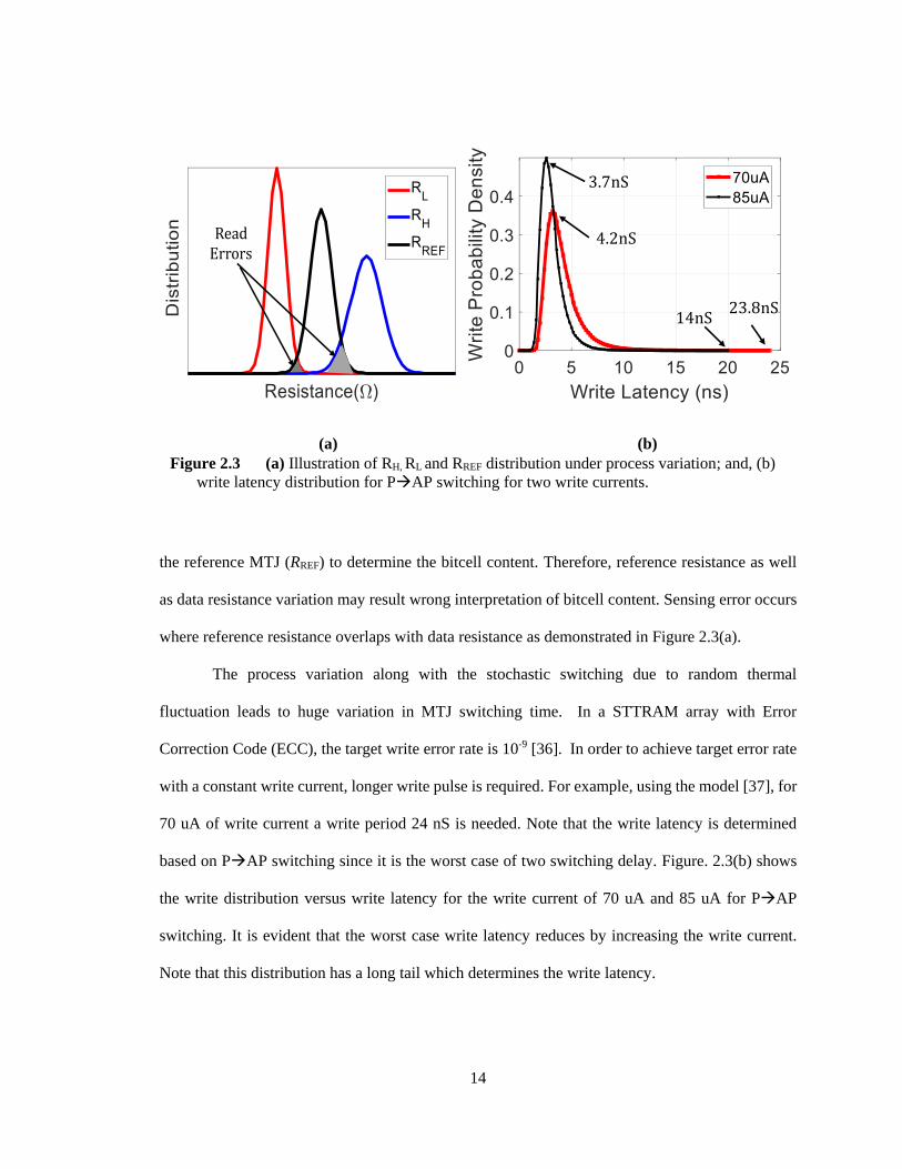
the reference MTJ (RREF) to determine the bitcell content. Therefore, reference resistance as well
as data resistance variation may result wrong interpretation of bitcell content. Sensing error occurs
where reference resistance overlaps with data resistance as demonstrated in Figure 2.3(a).
The process variation along with the stochastic switching due to random thermal
fluctuation leads to huge variation in MTJ switching time. In a STTRAM array with Error
Correction Code (ECC), the target write error rate is 10-9 [36]. In order to achieve target error rate
with a constant write current, longer write pulse is required. For example, using the model [37], for
70 uA of write current a write period 24 nS is needed. Note that the write latency is determined
based on P→AP switching since it is the worst case of two switching delay. Figure. 2.3(b) shows
the write distribution versus write latency for the write current of 70 uA and 85 uA for P→AP
switching. It is evident that the worst case write latency reduces by increasing the write current.
Note that this distribution has a long tail which determines the write latency.
(a) (b)
Figure 2.3 (a) Illustration of RH, RL and RREF distribution under process variation; and, (b)
write latency distribution for P→AP switching for two write currents.
Read Errors
3.7nS
4.2nS
14nS23.8nS
Page 38
15
2.1.3.4. Sense Margin
In order to sense the state of MTJ, data MTJ resistance can be compared against reference
MTJ resistance (which is an average of fixed high and low MTJ resistances). In conventional non-
destructive voltage sensing, sensing is performed by applying a current into both data and reference
MTJ and comparing the output voltage of data MTJ against that of reference MTJ. Due to poor
TMR, the voltage/current differential between RH and RL decreases which degrades the sense
margin. Furthermore, process variation reduces this difference even further (as shown in Fig.
2.3(a)) leading to a poor sense margin. Poor sense margin results in a wrong interpretation of MTJ
state.
2.1.3.5. Read disturb
As mentioned earlier, in order to prevent read disturbance IRead must be less than critical
current (IC). IC depends on current pulse width as follows [4]:
𝐼𝐶 = 𝐼𝐶0 1 − (𝐾𝐵𝑇
𝐸𝐵) ln(
𝑡
𝜏0) (2.4)
Where IC0 is the critical switching current at 0 K. EB is the barrier height, 𝜏 is the switching
time and 𝜏0 represents the inverse of the attempt frequency. The read current must be much smaller
than the median IC because repeated write cycles result in a wide variation in IC [38-39] to ensure
non-destructive read.
2.1.3.6. Data Security
STTRAM brings new data security issues that were absent in volatile memory counterparts
such as Static RAM (SRAM). This is primarily due to the fundamental dependency of this memory
technology on the ambient parameters such as the magnetic field and temperature that can be
exploited to tamper with the stored data. The free layer of MTJ flips under the influence of external
Page 39
16
magnetic field and temperature that can be exploited by the adversary. As described in Equation
2.1, the adversary can place an external AC/DC magnetic field to alter the Heff parameter resulting
in an uneven flipping of bits under read, write and/or retention [40]. The magnetic field produced
by a horseshoe magnet can be used to flip the bits in a STTRAM memory array [40]. Consequently,
the magnetic field can be exploited by the adversary for scrambling the data in LLC to launch denial
of service (DoS) attack or simply increase the miss rate affecting the overall performance of the
system. The existing countermeasures to mitigate the magnetic attack include variable strength
Error Correcting Code (ECC) and forced retention [40]. The strength of the ECC is increased
(1bit/2bit/4bit/8bit) depending on the magnitude of the attack. A carefully orchestrated DoS attack
can result in a severe consequence during the secure data processing and financial transactions to
name a few. The magnetic attack can also be carried out when the system is OFF. However, such
attacks will not affect the computation as the cache is invalidated on startup. The attacker can gain
access to non-volatile data after the authentic user has signed out, by launching unauthorized read
and write operation and probing the data buses [92].
Figure 2.4 Schematic of a conventional Domain Wall Memory. The MTJ at read and write
head and the overhead bits are also shown.
Page 40
17
2.2. Design Fundamentals of DWM
2.2.1. Basics of DWM
DWM consists of three components: (a) write head, (b) read head, and (c) magnetic
nanowire (NW). The read and write heads are similar to the conventional magnetic tunnel junction
(MTJ) whereas NW holds the bits in the form of magnetic polarity (Fig. 2.4). The left (right)
orientation can be regarded as ‘0’ (‘1’). The most interesting feature of the NW is the formation of
domain walls (DWs) between domains of opposite polarities where the local magnetization changes
its polarity. Dynamics of the NW is determined by the dynamics of DW. The DWs can be shifted
forward and backward by injecting the charge current from left-shift (LS) and right-shift (RS)
contacts. Note that the local moments change its orientation under the influence of current that
gives the impression of DW propagation in the NW. In essence, the NW is analogous to a shift
register. The new domains are injected by first pushing current through shift contacts to move the
bits in lockstep fashion to bring the desired bit under write head. Next spin polarized current is
injected through the write MTJ (using wBL and SL) in positive or negative direction to write a ‘1’
or ‘0’ in the NW. Read is performed by bringing the desired bit under read head using shift and
sensing the resistance of MTJ formed by DW under the read head (using rBL). It should be noted
that this new access mechanism makes shifting of DWs critical to the functionality of the memory.
The robustness, speed and power consumption of the memory has a significant dependency on DW
dynamics in the NW. A number of points that can be observed in this context are: (a) read and write
operation is linked with shifting of bits, (b) buffering of bits is required to ensure that the useful
bits are preserved in the NW. Therefore, only a fraction of bits from the NW can be used for
computation defined as ‘utilization factor’ (UF), and (c) the shift latency depends on the offset from
read/write heads. Hence, multiple heads are desirable to reduce the access latency, and (d) bitcell
footprint depends on both the NW dimensions as well as the number and size of read/write heads.
Page 41
18
2.2.2. Modeling of DWM
For the read and write head we utilized the hspice model of MTJ from nanohub [37]. The
DW dynamics in the NW is modeled in verilog-A by solving the Landau-Lifshitz-Gilbert (LLG)
for 1D motion [41]:
(1 + 𝛼2) =𝜇0
2𝛾Δ(𝐻𝑘 sin 2𝜓 − 𝜋𝐻𝑇) + 𝛼Δ𝛾 (𝜇0𝐻𝐴 −
𝑉𝑞
𝑀𝑠𝑑) + (1 + 𝛼𝛽)𝑢 (2.5)
(1 + 𝛼2) = −𝜇0
2𝛼𝛾(𝐻𝑘 sin 2𝜓 − 𝜋𝐻𝑇) + 𝛾 (𝜇0𝐻𝐴 −
V𝑞
𝑀𝑠𝑑) +
𝛽−𝛼
Δ 𝑢 (2.6)
Where, and are the time derivatives of the domain wall position and tilt angle
respectively, α is the damping constant, β is the non-adiabatic spin torque transfer term, V is pinning
potential, d is the pinning notch width, ∆ is DW width parameter, Ms is saturation magnetization,
Hk is demagnetization field, HA and HT is applied field and u is a scalar quantity having the unit of
velocity. Term u depends on the current density J, the spin polarization P, saturation magnetization
𝑀𝑠 and Bohr Magneton 𝜇𝐵 as follows:
𝑢 =𝜇𝐵𝐽𝑃
𝑒𝑀𝑠, 𝜇𝐵 =
ℏ𝑒
2𝑚𝑒 (2.7)
Table 2.2 Magnetic constants used for DW dynamics.
Parameter Value
α Varied (0.01 - 0.02)
β Varied (0.0 - 0.1)
Bohr magneton(µB) 9.27e-24 J/T
Ms 8e5 A/m
Exchange Constant (A) 1.3e-11 J/m.
Length(l)/Width(w)/Thickness(t) of NW 1e-6 m/1e-7 m/10e-9 m
ɣ 1.76e11 /G s
Demagnetization Field (Hk) 1600~1800 Oe.
Page 42
19
The detailed derivation of the above equation from LLG is provided in [11]. The values of
constants used in the model are provided in Table 1. The DW velocity depends on the shift current.
Higher current increases the DW velocity but increases the power consumption.
2.2.3. DWM Challenges
The DWM read and write heads are similar to conventional magnetic tunnel junction
(MTJ), whereas NW acts as free magnetic layer, and holds the bits in the form of magnetic polarity.
Hence, DWM design challenges includes all the challenges associated with MTJ such as limited
TMR, stochastic switching, read disturb, and oxide breakdown as described in Section 2.1.3.
However, there are other challenges involved with DWM:
2.2.3.1. Shift Latency
As mentioned earlier, shift operation is required to access a bitcell in DWM. The time
needed to access a bitcell on a NW depends on its location with respect to the read/write port.
Moreover, multiple shift operations are performed in single memory access to read/write all bits of
data which poses significant latency and power overhead.
2.2.3.2. Segregated Read and Write Head
The conventional DWM contains segregated read and write heads (Fig. 2.4) to decouple
read and write and make head design simple. Although it simplifies the design constraints due to
separate read/write head design, this design incurs loss in bitcell density due to the dedicated access
transistor and wiring for each head. Furthermore, the separate read and write heads is functionally
redundant since both read and write operations cannot be performed simultaneously (unless the
shifts need for read and write are identical). This makes the read head to wait until the write head
has finished writing and appropriately shifts back the bits into its original place or vice versa.
Page 43
20
2.2.3.3. Aspect Ratio Mismatch
DWM suffers from aspect ratio mismatch between NW and access transistor, since the NW
is long and narrow and access transistor is wide. Therefore, DWM layout must be optimized to
achieve the maximum memory density. In addition, since the shift circuitry is shared among all the
local columns in a global column, the shift operation shifts all the NWs at the entire global column.
This incurs substantial shift power overhead. Therefore, a gating mechanism is needed to avoid
shifting of unassessed NWs.
2.2.3.4. Utilization Factor (UF)
As mentioned earlier, a certain number of bits per NW are dedicated for buffering the
functional bits during shift. The number of heads and their positioning in the NW determine the
amount of buffer space required for preserving the functional bits. For better bitcell density it is
desirable to achieve higher UF which in turn depends on the number of heads, their positioning and
the physical dimension of the NW.
(a) (b) (c)
Figure 2.5 (a) Schematic of the 1T1R structure of RRAM; (b) schematic of the 1D1R
structure of RRAM; and, (c) I-V curve of bipolar switching.
Metal Oxide
BE
TE
Metal Oxide
BE
TE
BL
WL
SL
BL
WL
ITIRITIS
1.00E-07
1.00E-06
1.00E-05
1.00E-04
1.00E-03
1.00E-02
1.00E-01
1.00E+00
-2 0 2
Curr
ent(
A)
Voltage(V)
I-V Sweep
SET
RESET
Page 44
21
2.3. Design Fundamentals of RRAM
2.3.1. Basics of RRAM
As discussed in the first chapter, RRAM is a promising candidate to replace main memory
due to small footprint and low standby power. The device structure is an oxide material sandwiched
between two metal electrodes (i.e., Top Electrode (TE) and Bottom Electrode (BE)) called metal-
insulator-metal (MIM) structure (Fig. 2.5(a)). RRAM bitcell consists of MIM and a selector device
which can be either a transistor (1T1R structure as show in Fig. 2.5(a)) or a selector diode (1D1R
structure) as shown in Fig. 2.5(b). The 1T1R cell provides the small footprint of 6 F2 whereas
footprint as low as 4 F2 can be achieved by 1D1R structure in crossbar memory architecture. There
are two types of resistive switching. One type is based on the formation of conductive filament
(CF) consisting of oxygen vacancies which occurs in oxide-based RRAM. The second type is based
on the conductive filament of metal atoms which is called conductive-bridge RAM (CBRAM). The
oxide-based RRAM resistive switching is basically due to the mechanism of oxide breakdown
which forms a conduction filament in the oxide. The switching from High Resistance State (HRS)
to Low Resistance State (LRS) is called “SET” process, while the opposite switching is called
“RESET” process. Usually, fresh RRAM samples require a voltage greater than SET voltage to
Figure 2.6 Forming, SET and RESET switching mechanism in RRAM.
TE
BE
V=VForming
BE
CF
TE
V=VReset
BE
Residual Filament
TE
HRS
Oxygen AtomOxygen IonOxygen Vacancy
Tunneling Gap
BE
TE
VSET
Resetset
BE
LRS
Forming
Page 45
22
trigger the resistance switching for the next cycles, which is known as the “forming” process. The
resistive switching can be categorized into unipolar and bipolar switching. In unipolar RRAM,
switching direction depends on the amplitude of the voltage across RRAM and does not depend on
the polarity of applied voltage. Therefore, SET/RESET can take place at the same polarity. In
bipolar switching, switching direction depends on the polarity of applied voltage. Thus, SET only
occurs at positive polarity, while RESET occurs at negative polarity as shown in Fig. 2.5(c).
Typically, in oxide-based RRAM, resistive switching is associated with migration of
oxygen ions between electrodes, resulting in the formation of conduction filament. As
demonstrated in Fig. 2.6, during the forming process, soft dielectric breakdown due to high electric
field leads to the drift of oxygen ions to anode interface. If the anode material is a noble metal, the
oxygen ions are discharged as neutral non-lattice oxygen, while they react with oxidizable anode
materials to form an interfacial oxide layer [42]. Therefore, the electrode/oxide interface acts as an
oxygen reservoir [43]. In the LRS mode, the current flows through the CF. In the reset process,
oxygen ions migrate back to the bulk to recombine with the oxygen vacancies which in turn reset
the RRAM to HRS. In this thesis, switching model of HFO2 based bipolar RRAM is used. HFO2
has gained significant attention due to properties such as simplicity, low operating power and high
speed [44].
2.3.2. RRAM Design Challenges
Even though RRAM provides good design metrics such as high density, low standby
power, fast access time, and high resistance ratio, it suffers from low endurance, process variation,
nonuniformity, and requires low-read voltage for prevention of read disturbance.
To avoid a permanent dielectric breakdown in the set process, it is essential to limit the
current called compliance current. During formation/SET process, when CF is formed in the oxide
material, the current flowing through RRAM increases abruptly. Therefore, a current limiter is
Page 46
23
required to clamp the forming/SET current in order to prevent degradation of HRS and failure of
memory device [45]. Due to lower high resistance at saturation region a transistor is a better current
limiter. Large capacitance between transistor and RRAM must be avoided in design of 1T1R
bitcell. Parasitic capacitance results in overshoot current during SET process which in turn
increases the SET current.
RRAM suffers from poor nonuniformity due to extensive parameter variation such as
variation of switching voltage as well as resistance variation in LRS and HRS. The variation of
resistance switching includes temporal variation (cycle-to-cycle) and special variation (device-to-
device). These variations are originated from the stochastic nature of the oxygen vacancies/ion
process [46].
High density crossbar array which employs two terminal RRAM at the crosspoint of
vertical and horizontal metal wires are proposed [47]. Nonetheless, these architectures suffer from
sneak-path problem entailing a poor sense margin, higher power consumption, and limited array
size.
Page 47
24
Chapter 3
3. Robust and Low Power STTRAM Design
Conventional CMOS memory i.e., Static Random Access Memory (SRAM) has been the
popular choice for embedded memory application for last several decades. However, SRAM seems
to be approaching a brick wall. On one hand process variability and leakage power is posing severe
obstruction towards SRAM scaling to future nodes and on the other hand, emerging energy-
constrained and bandwidth hungry electronic gadgets demand for larger as well as energy-efficient
on-chip cache which cannot be satisfied with SRAM. To address the changing landscape of
consumer market, there is a corresponding need of changing the design paradigm. Several emerging
memory technologies are on the horizon such as STTRAM, DWM and RRAM but there is no clear
universal choice for embedded application. STTRAM is promising for Last Level Cache (LLC)
due to numerous benefits such as high-density, non-volatility, high-speed, zero leakage, CMOS
compatibility [48] and good endurance [4]. The crucial challenges involved in STTRAM are high
write energy, long write time and poor sense margin. In this chapter, we propose circuit and
architectural techniques to improve read yield, write latency and write power of STTRAM.
3.1. Introduction
Implementation of last level cache using STTRAM is widely investigated. It is accepted
that STTRAM reduces the leakage power substantially. In [49] STTRAM is compared against
SRAM and DRAM in a single-core processor architecture in terms of area, energy and
performance. Then they have explored 3D microprocessor stacking with MRAM. Authors have
explored STTRAM cache in multi-processor architecture and investigated costly write operation in
Page 48
25
STT-RAM on power and performance [51]. Architectural evaluation of replacing on-chip DRAM
with STTRAM has been investigated [50]. Authors proposed a dual-write-speed STTRAM
architecture which benefits from the correlation between MTJ device write time and write current
[53]. This method offers write latency improvement with relatively small memory cell size. The
relationship between write latency and retention time to find optimal retention-time for STTRAM
LLC has been explored in [54]. This paper explores adapting data retention time to match the
required refresh time of LLC blocks to improve performance and save energy. Most of these works
report more than 10% performance degradation due to employing STTRAM LLC architecture.
Many works have been made to address the performance and energy overhead of STTRAM LLC.
Architectural optimization has been proposed to recover dynamic energy due to store instruction
by coalescing stores from L1 to the L2. The idea is to increase the residency of dirty lines in the L1
to accommodate all the stores to that line. This would prevent the line from being prematurely
evicted to the L2 and being subsequently move back to the L1 on a near term store miss [58]. In
[52], a hybrid design of SRAM L1 caches STTRAM L2 and L3 caches is proposed. Device-
architecture space is explored to reduced write power by lowering the thermal energy to trade
volatility [55-57]. It can be concluded that STTRAM is great potential to be used as an on-chip
random access cache due to high density and low standby power. Moreover, circuit and
architectural improvement can be employed to mitigate long write latency to achieve similar
performance as that of SRAM cache. In this chapter, we investigate circuit and micro-architectural
techniques to address these design challenges.
Due to poor TMR, the voltage/current differential between RH and RL decreases which
degrades the SM. Furthermore, process variation reduces this difference even further results in poor
sense margin. In this chapter, we propose, slope sensing, a destructive sensing technique to
eliminate reference resistance variation. In addition, we propose a non-destructive sensing scheme
Page 49
26
that exploits a voltage feedback and boosting (VFAB) technique to develop large sense margin.
This technique reduces the sensing power significantly by eliminating static current.
We observe that process variation can result in large spread in write and read latency
variations. The performance of conventionally designed STTRAM cache can degrade as much as
10% due to process variations. We propose a novel and adaptive write current boosting to address
this issue. In this method, the bits experiencing worst-case write latency are fixed through write
current boosting.
In summary, we make following contributions in this chapter:
• We propose a destructive slope detection technique using sampling techniques in order to
detect MTJ resistance when it switches from high to low resistance state. We have designed
a test-chip and performed thorough characterization. We characterized the slope sensing
technique with respect to various design parameters such as sampling frequency, ramp
current slope, TMR and various flavor of MTJ resistance.
• We propose a low-power and robust STTRAM sensing which exploits voltage feedback
and boosting (VFAB) techniques to achieve large sense margin. We perform detailed
process and temperature variation analysis to evaluate robustness of VFAB technique.
• We investigate the impact of process variations on the write latency of STTRAM and
propose a methodology to enable write current modulation adaptively to mitigate process
variation induced write latency degradation.
3.2. Improving Read Yield of STTRAM Array
Sense margin of STTRAM depends on TMR `which is defined as 100*(RH-RL/RL) where
RL and RH are low and high resistance of MTJ respectively. Due to poor TMR, the voltage/current
differential between RH and RL decreases which degrades the SM. Furthermore, As described in
Page 50
27
Section. 2.1.3.3, process variation induces large spread in low and high resistance states. The
limited TMR and process variation result in poor sense margin. Poor sense margin can result in
wrong interpretation of the MTJ state. The STTRAM sensing can be categorized into non-
destructive and destructive sensing. In conventional non-destructive voltage sensing, data MTJ
resistance is compared against reference MTJ resistance (which is an average of fixed high and low
MTJ resistances). Therefore, it suffers from reference resistance variation in addition to data
resistance variation. Moreover, sensing is associated with applying a static current into data leg and
two reference legs which results in high power consumption. In addition, non-destructive sensing
suffers from read disturb. Destructive sensing involves with writing into bitcell that results in
significant power and latency overhead. However, destructive sensing eliminates bit-to-bit process
variation in MTJ resistance which in turn improves read yield drastically. In addition, ` it suffers
from failures due to unoptimized selection of data and reference currents.
In this Section, we investigate two sensing techniques to improve sense margin. First, we
propose a novel slope detection technique to exploit MTJ resistance switching from high to low state
using low-overhead sample-and-hold circuit. The proposed sensing technique is destructive in nature
and eliminates reference resistance variation. Second, we propose a non-destructive and low-power
sensing scheme that exploits a voltage feedback and boosting (VFAB) technique to develop large
Figure 3.1 Taxonomy of STTRAM sensing schemes.
Non-Destructive
Sensing
Destructive
Voltage Mode[59]
Self-ReferenceVoltage [65]
Slope Detection
(proposed)
Self-Reference [67]
Current Mode [64]
Negative Resistance
[62]
Source -Degeneration
[60]
Page 51
28
sense margin. Furthermore, VFAB does not requires a static current to be injected into data and
reference STTRAMs which results in significant power saving.
3.2.1. Classification of Sensing Techniques
Fig. 3.1 shows the taxonomy of various sensing techniques. STTRAM sensing can be
broadly categorized into destructive and non-destructive sensing. Several techniques have been
proposed under non-destructive sensing. A non-destructive voltage sensing and a sizing
methodology to improve the SM of MRAM arrays has been proposed in [59]. Source degeneration
scheme is proposed in [60][91] to reduce large sense margin variation. Self-body biasing technique
has been proposed in [61] to resolve the small sense margin issue in conventional voltage sensing
scheme. In this scheme threshold voltage of load PMOS transistor is adaptively controlled by body
bias. Negative resistance read and write technique has been described in [62] to eliminate read
disturb and reduce the write power. Reference voltage (Vref) biasing has been explored in [63] to
shift margins between polarities to improve the robustness. A non-destructive current mode
sensing scheme using current conveyor has been proposed in [64]. In [65-66], a
nondestructive self-reference sensing scheme has been proposed by leveraging the dependency of
high and low resistance state of the MTJ on the cell current amplitude. Even though this scheme
reduces the read latency and power by eliminating two write steps, the sense margin is much smaller
than destructive self-reference scheme and conventional nondestructive voltage sensing.
Under destructive sensing, a self-reference sensing has been proposed in [67] to eliminate
bit-to-bit process variation in MTJ resistance. Sensing is performed by first storing the voltage of
the MTJ by passing a current (I1), and then after a time interval storing a reference voltage of the
same MTJ by passing current (I2). The variation in MTJ resistance can be eliminated using this
self-reference sensing scheme. Although this mechanism incurs high power consumption and long
Page 52
29
read latency due to two write steps, it provides high sense margin and eliminates the need of
reference voltage.
3.2.2. Background
3.2.2.1. Non-destructive Voltage Sensing Scheme [59]
The sense circuit identifies the resistance of the data MTJ. In order to make the comparison,
data MTJ resistance is compared against reference MTJ resistance (which is an average of fixed
high and low MTJ resistances). Fig. 3.2 (a) shows the typical voltage sensing where a reference
current is injected in both data leg and reference legs and the resulting voltage is compared by a
voltage sense amplifier. Poor sense margin can result in wrong interpretation of the MTJ state. For
example, if the offset voltage of the sense amplifier (SA) is +/-25mV, a sense margin of 25mV can
be read as either ‘0’ or ‘1’.
3.2.2.1.1. Impact of process variation
MTJ model [37] is used in order to perform process variation analysis. Process-variations
for read operation is modeled by incorporating variations in MTJ as well as access transistor [68].
For MTJ we have assumed tunnel oxide barrier and surface area variations. The variations in access
transistor is lumped in threshold voltage fluctuation. The mean and standard deviation of these
Table 3.1 Parameters used for process variation study.
Device Parameter Mean Std. Dev.
PMOS VTH 460 mV 𝐴𝑉𝑇/√𝑤𝐿
NMOS VTH 500 mV 𝐴𝑉𝑇/√𝑤𝐿
MTJ
MgO Thickness 1.2nm 2%
Shape Area 100nm*50nm 10%
Page 53
30
parameters are provided in Table 3.1. In non-destructive sensing, resistance of data MTJ is
compared against the resistance of reference MTJ to determine the bitcell content. Therefore,
reference resistance as well as data resistance variation may result in wrong interpretation of bitcell
(a) (b)
Figure 3.2 (a) Non-destructive sensing scheme; (b) Data0, reference and Data1 voltage
distributions.
(a) (b)
Figure 3.3 SM0 and SM1 distribution for 10000 Monte-Carlo points; (a) original scheme
[59]; and, (b) with source degeneration [60].
RH RL RD
WL
ysel
VClamp
PLR0
DataReference
VRef
Vdata1/0
Sense Amp
PLR1
PLD
NYD
NCDNCR0
NAR1 NAR0 NAD
PDDPDR0PDR1VDgen
NCR1
NYR1NYR0
PREPRE
VData1
VData0
VRef
I
R
0 0.5 10
2000
4000
6000
Voltage(v)
Dis
trib
utio
n
Vdatah
VdatalVData0 :μ=0.17 σ=0.1VData1:μ=0.81 σ=0.18VRef:μ=0.41 σ=0.003
VData0
VData1
VRef
-0.6 -0.4 -0.2 0 0.2 0.40
50
100
150
200
250
300
350
Sense Margin(v)
Dis
trib
utio
n
SM0
SM1
SM0 FailuresSM1 Failures
25mV SA offset
Failure ratio_50mV offset= 13.5%
Failure ratio_25mV offset= 10.7%
-0.6 -0.4 -0.2 0 0.2 0.40
100
200
300
400
500
600
Sense Margin(v)
Dis
trib
utio
n
SM0
SM1
25mV SA offset
Failure ratio_50mV offset= 8 %
Failure ratio_25mV offset= 6.9%
SM0 Failures
SM1 Failures
Page 54
31
content. Data0, Data1 and reference voltage distributions and RH, RL and RRef resistance
distributions are shown in Fig. 3.2(b). Sensing error occurs where reference voltage overlaps with
Data0/1 voltage.
Two critical transistors in STTRAM sense circuit are the PMOS load (PL) and NMOS
clamp (NC) (Fig. 3.2(a)). The clamp voltage and clamp transistor size sets the current in the leg.
The load transistor sets the output voltage (where the NMOS and PMOS drain currents intersect).
The mismatch between matched-pair transistors in the sense circuit degrades the sense margin.
Since size of PL is smaller than NC transistor, the sense margin is most sensitive to mismatch
between the PL transistors of reference legs (PLR) with that of data leg (PLD). One sigma of VT
variation is given by following equation [68]:
𝜎𝑉𝑇 =𝐴𝑉𝑇
√𝑊.𝐿 (3.1)
Where W and L are the width and length of the transistor and 𝐴𝑉𝑇 is pelgrom coefficient.
Sense circuit is designed to reduce the impact of process variation on SM. This goal is achieved
by increasing the width and length of PL transistors to reduce the VT mismatch between PLD and
PLR, and optimizing other design parameters (NC width, Vclamp and VRef) to maximize both SM0
Figure 3.4 The impact of clamp voltage on sense margin for VClamp=0.7V and VClamp=0.9V.
NCD(Data-1)NCD(Data-0)PLD
PLR
NCD(Data-1)NCD(Data-0)PLD
PLR
VDSVDS
SM0=200mV
SM0=284mV
SM1=337mVSM1=431mV
Vclamp=0.7V Vclamp=0.9V
Page 55
32
and SM1. Distributions of SM0 and SM1 for 10000 Monte-Carlo points are depicted in Fig. 3.3
(a). Simulations reveal that 10% of bitcells fail sensing due to SM0 failures and 11.2% fail due to
SM1 failures which result in 10.7% total failures for 25mV SA offset. It is evident that non-
destructive conventional sensing is prone to process variation. To reduce the large sense margin
variation, the source degeneration scheme is used with longer channel length for PL transistors
[60]. Source degeneration PMOS (PD) is added to the source of PL transistors to reduce current
variation and increase effective resistance which results in SM improvement. Fig. 3.3(b) shows
SM0 and SM1 distributions for 10000 monte-carlo points with source degeneration scheme. The
simulation reveals 4.7% SM0 failures and 11% SM1 failures which result in 6.9% total failures for
25mV SA offset. Although source degeneration reduces SM0 failures, SM1 failures are still
significant which underscores the need for a self-reference scheme to eliminate bit-to-bit variation
as well as the mismatch between matched-pair transistors in data and reference legs.
As shown in Fig. 3.4, as clamp voltage increases SM0 reduces while SM1 increases.
Therefore, clamp voltage can be exploited as a knob to make a trade of between SM0 and SM1 to
minimize the sensing failures. The mismatch between matched-pair transistors in the sense circuit
as well as reference resistance variation degrades the sense margin.
3.2.2.2. Destructive Self-reference Sensing Scheme [67]
In self-reference sensing, voltage generated by the data current across the MTJ, and the voltage
generated by a reference current across the same MTJ are compared. Therefore, the bit-to-bit
variation in MTJ resistance is eliminated. Self-reference sensing scheme works as follows (Fig.
3.5):
Page 56
33
1) A read current IData is injected into bitcell and the resulting voltage is stored in a capacitor
C1. The voltage could be VDataH (VDataL) if the MTJ resistance is high (low).
2) A zero is written into the MTJ.
3) Another read current IRef is applied to generate voltage VRef which is stored in capacitor C2.
4) VData and VRef are compared to determine the bitcell content.
5) The read data is written back to the MTJ.
(a) (b)
Figure 3.5 (a) Self-reference sensing scheme; and, (b) sense circuit timing diagram is also
shown.
Figure 3.6 I-R characteristics of the two MTJs under process-variation. A variation in
resistance can change the sense margin.
WL
MTJ
YSEL
Ref Data
C1
VRef
Output
VDD
S2S1
T2 T1
T3
T4
VData
C2
TS1 TS2
Coupling Capacitors
VMTJ
IREF/IData
VDD
SENS1
S2
SEN
0.5 4.5 5
IData
IRef
MTJ Write Time
WL
0Time(nS)
IData IRef
A1
VDataH
Vref
RL
RH
I
R
A2A3
A1=VDataH =IData*RH
A2=VDataL=I Data*RL
A3=VRef= Iref *RRef
VDataL
MTJ1MTJ2
Bitline
Source line
wordline
MTJ
Page 57
34
Considerations for process-variations is important to determine appropriate values of IRef
and IData. I-R curves of the two MTJs under process variation are shown in Fig. 3.6. If a current is
injected from bitline to source line, MTJ switches from high-to-low resistance state. In contrast, if
a current is injected from source line to bitline the MTJ is switches from low-to-high resistance
state. The IData and IRef must be chosen in such a way that to make SM0 positive and SM1 negative.
Therefore, the area A3 (which is essentially voltage) should be greater than A2 and less than A1,
which results in following inequalities:
𝑉𝐷𝑎𝑡𝑎𝐿 < 𝑉𝑅𝑒𝑓 < 𝑉𝐷𝑎𝑡𝑎𝐻 (3.2)
𝑆𝑀0 = 𝑉𝑅𝑒𝑓 − 𝑉𝐷𝑎𝑡𝑎𝐿 > 0
𝑆𝑀1 = 𝑉𝑅𝑒𝑓 − 𝑉𝐷𝑎𝑡𝑎𝐻 < 0
3.2.2.2.1. Impact of process variation:
To understand the impact of process variation on data and reference current requirement
we sweep the bitcell current from bitline to source line. If the bitcell state is low, the voltage across
MTJ increases monotonically with current. However, if the bitcell state is high, it switches to low
resistance state beyond the critical current. Therefore, the voltage changes from high-to-low. As
depicted in Fig. 3.7, IRef and IData should be chosen carefully to ensure +ve SM for high data and –
ve SM for low data. Therefore, VRef should be greater than VDataL and less than VDataH where VDataL
(VDataH) is the voltage across the MTJ when the stored data is low (high). From Fig. 3.7(a), the
optimum IData is the current which maximizes SM0+SM1 (i.e., the current where VDataH is
maximum). Optimum IRef is chosen in such a way to equalize SM0 and SM1. Fig. 3.7(b) shows the
optimum IData variation which results in optimum IRef variation. We have evaluated two cases for
determining robust reference and data current:
Page 58
35
Case-(a) (Optimum): data and reference currents are bit-to-bit optimal to maximize the
sense margins.
Case-(b) (IData-Mean, IRef – Mean): both data and reference current are the mean value of
the current distribution.
Fig. 3.8 shows the SM distribution for 5000 Monte-Carlo points for cases (a) & (b). Case-
(a) provides a distribution with lowest standard deviation and higher mean value which results in
good sense margins for all bitcells and provides minimum number of failures. However, the number
(a) (b)
Figure 3.7 (a) V-I curves of an MTJ with high and low resistance states initially; and, (b)
optimum data current variation.
Figure 3.8 Sense margin distribution for 5000 Monte Carlo points.
IData-
Optimium
IRef-
Optimum
VDataL
VRef
SM1
SM0
V
I
VDataH
0 20 40 600
0.1
0.2
0.3
0.4
0.5
Voltage(V
)
Current(uA)
Idata Variation
-0.1 -0.05 0 0.05 0.1 0.150
100
200
300
400
500
600
700
Sense Margin
Dis
trib
ution
Idata-Mean,Iref-Mean
Optimum
Failures
SM1 SM0
25mV offset
Failure ratio_50mV offset= 16%Failure ratio_25mV offset= 1.8%
Page 59
36
of failures increase significantly (failure ratio of 1.8%) in case-(b). In addition, SM failure ratio
increase to 16% for case-(b) for 50mV SA offset. Even by providing optimum data and reference
current for each bitcell, failure ratio is 9.5% for 50mV SA offset. Hence, there is a need to develop
a sensing scheme which eliminates data and reference current.
3.2.3. Proposed Slope Sensing Technique
To eliminate bit-to-bit process variation as well as data and reference current, we propose
a reference-less, destructive slope detection technique which exploits the MTJ switching from high
to low state to detect memory state. We design a proof-of-concept test-chip using 96kb mimicked
STTRAM (using passive resistors) bits in 65nm technology to validate the proposed slope sensing
circuit. The resistor values are matched with the experimentally calibrated simulated models to
capture the process variations in real MTJ. A single mimicked STTRAM bitcell contains both low
and high resistors in parallel and the switching circuit is designed to match the switching latency
of real MTJ.
(a) (b)
Figure 3.9 (a) Slope detection sense circuit; and, (b) simplified timing diagram.
WL
MTJ
YSel
IRamp
VDD
Buffer
s+-
Sense Amp
VMTJC1
C1dSE
∅ 𝑑
∅
`
VBUFO
VC1
VC2
Time
𝐿
∅ 𝑑
∅ Sample1
Sample2
VC1d<VC1 VC1<VC1d
VMTJVC1
VC1d
Page 60
37
3.2.3.1. Slope Sensing Basic Operation
If the MTJ resistance is low, it will only switch with a negative current. The resistance will
remain low for positive current. We also note that slope of MTJ V-I curve changes from positive
to negative during switching of resistance. Therefore, we propose to sense the change in slope of
voltage to detect the MTJ state. A ramp current is injected into bitcell which results in a ramp
voltage. If the MTJ resistance state is high initially the slope of voltage will change from positive
to negative as the MTJ resistance switches from high to low resistance state while the voltage slope
will remain positive if the resistance of MTJ is low initially. Therefore, sensing problem can be
simplified to slope detection. If a negative slope is detected then the data is sensed as ‘1’, else the
data is sensed as ‘0’. We used high speed sample and hold circuit to detect the slope of voltage
across bitcell (Fig. 3.9(a)).
Fig. 3.9(a) shows the proposed sensing circuit with features to inject the ramp current and
sample the ramp voltage. The slope of ramp voltage will change from positive to negative if the
MTJ switches from high to low resistance. The voltage slope remains positive if MTJ resistance is
initially low. The slope detection is performed by sampling the ramp voltage with two sample-and-
hold circuits using clocks ϕ1 and ϕ1d (delayed ϕ1). The sampled voltages are stored in C1 and C1d
respectively. Finally, VC1 and VC1d are compared at the edge of sense amplifier enable (SE).
Simplified timing diagram is shown in Fig. 3.9(b).
As shown in Fig. 3.10(a), white triangles are voltages sampled by ϕ1 and black triangle are
voltages sampled by ϕ1d. The sense amplifier is enabled after the black triangles. As a result, two
consecutive black and white triangle sampled voltages are compared. It is evident that the SM is
Page 61
38
positive in positive slope region and negative in the negative slope region. Sense margin depends
on sampling frequency, slope of ramp current and MTJ switching time. We have implemented
design-for-test features to test the sensing failure by sweeping these parameters. By increasing the
ramp current slope, the voltage difference between two consecutive samples will increase which
results in higher SM. However, the buffer output voltage (VBUFO) may be clamped at VDD by further
increasing the ramp current slope which results in SM loss.
(a) (b)
(c) (d)
Figure 3.10 Sampling voltage across MTJ: (a) sampling with frequency f1 and ∅1-∅1d clock
phases which provides poor SM0 and large SM1; (b) sampling with frequency f2 (f2= f1/2) and ∅1-∅1d clock phases which provides large SM0 but poor SM1; and, (c) double sampling with
frequency f2 , ∅1-∅1d and ∅2-∅2d clock phases which results in large SM0 and SM1 while ensure
capturing negative slope.
time
V
SM0
(f1)
SM1
Sampling delay
Frequency= f1
V
time
SM0
SM1
Sampling delay
Frequency= f2
V
time
SM1
SM0
Sampling delay
Frequency= f2
V
SM0
SM1
SM1
SM0
Frequency= f2
time
2- 2d
1- 1d
Page 62
39
3.2.3.2. Double Sampling
Fig. 3.10 shows impact of two sampling frequencies on sense margin. Note that lower
sampling frequency results in more Sense-0 Margin (SM0) since the voltage difference of two
consecutive samples is higher as shown Fig. 3.10(b). However, decreasing sampling frequency
might cause an error in negative slope detection due to poor SM1. Sampling at higher frequency
ensures negative slope detection. However, SM0 loss due to higher sampling frequency results in
increased failures (Fig. 3.10(a)). As shown in Fig. 3.10(b), sampling with frequency f2 (where f2 =
f1 /2) and ϕ1-ϕ1d clock phases provides poor SM1 after MTJ flipping while sampling with frequency
f1, ϕ1-ϕ1d, provides larger SM1. In order to obtain the desired number of samples at lower sampling
frequency to ensure negative slope detection (higher SM1) as well as higher SM0, double sampling
technique is proposed.
Double sampling can be implemented by lowering sampling frequency and using two sets
of sample-and-holds (S/H) with ϕ1-ϕ1d and ϕ2-ϕ2d clock phases (where ϕ2 and ϕ2d are delayed ϕ1 and
ϕ1d respectively) to sample voltage across bitcell. Hence two groups of sample-and-hold circuits
(SC) are used. From Fig. 3.10(d), sense amplifier is activated after ϕ2d (black circle) and ϕ1d (black
triangles). Therefore, SM is the difference between black and previous white circle voltages which
is sensed by 1st sense amplifier or black and previous white triangle voltages which is sensed by 2nd
sense amplifier. In the proposed double sampling method, if one of sense amplifiers detects
negative slope (SM1) the output is ‘1’ otherwise it is ‘0’. Therefore, the SM1 is the maximum
absolute value of SM1 which is provided by two sets of S/H circuits. From Fig. 3.10(b-c), it can be
noted that sampling with frequency f2 and ϕ1-ϕ1d provides poor SM1 while sampling with frequency
f2 and ϕ2-ϕ2d provides large SM1. Therefore, double sampling with both ϕ1-ϕ1d and ϕ2-ϕ2d clock
phases provides large SM1 as well as large SM0. Sampling is performed during sense time (TSenes).
Sense time is determined in such a way to ensure all bitcells in high resistance will switch to low
Page 63
40
resistance state under process variation. Note that sampling accuracy and robustness can be
improved by increasing the number of sample-and-holds and lowering the sampling frequency to
achieve larger SM1 and SM0 at the cost of more sense amplifiers.
3.2.3.3. Test Chip Implementation
In this section, we explain the subarray architecture with integrated slope sensing circuit
and the test chip design.
3.2.3.3.1. Slope Sensing Circuit Design
Fig. 3.11 depicts the implementation details of slope sensing with two SCs to enable double
sampling. To mimic MTJ resistance in the test-chip we used poly resistance. The bitcell contains
two high resistances (RH) and two access transistors (Fig. 3.11). The bitcell is in high resistance
state if WL1 is activated and is in low resistance state if both WL1 and WL2 are asserted (two RH
are connected in parallel). In order to mimic the switching time variation, we have incorporated a
knob to fire WL2 at different times. Our design matches the real MTJ parameters such as, MTJ
Figure 3.11 Implementation details of slope detection sense circuit.
RH
YSEL
VDD
`
Speed-up Transistor
Ts
TM3
TM1
TB1
TB2
∅
∅ 𝑑
C1
C1d
∅2
∅2𝑑
`
`
`
C2
C2d
SE1
OUT1
NORLatch
NORLatchSET
SET
LE1
LE1d
Data1Q
Q
SE2
OUT2
NORLatch
NORLatchSET
SET 2
LE2
LE2d
Data2
Q
Q
Ramp Voltage Gen.
V-I Conv
Bitcell
Data
SC1
SC2
Buffer
1
VBit
VBUFOTM2
BUFEN
WL1RHWL2
WL1
-
+
-
+
RST
Page 64
41
resistance, switching time and TMR variability using experimentally calibrated simulation models
[37] (details in Section 3.2.3.2.2) and serves as a solid proof-of-concept for the slope sensing
scheme.
The ramp current is generated using RC low pass filter to generate a ramp voltage. The
output of low pass filter is connected to gate of an NMOS transistor (TM1) to generate a ramp
current. Since the TM1 is OFF for voltages less than threshold voltage, a speedup transistor (TS) is
used to charge the capacitor rapidly to threshold voltage of TM1 in order to speed up the ramp current
generation process. Next, the ramp current is injected in to bitcell using a PMOS current mirror
Figure 3.12 Post layout simulation of slope sensing scheme along with timing diagram for
sense circuit-1(SC1) and SC2.
0 5 10 15 20 25 30
∅ ∅ 𝑑
VC1
VC1d
VBUFO
LE2
LE2d
∅2∅2𝑑
VC2
VC2d
VBUFO
Compare Compare
SM=-240mVSM=180mV
SE1
Time(nS)
SM=-300mVSM=190mV
WL2WL1
SE2
SC2
0.25
0.5
0.75
1
0.25
0.5
0.75
1
LE1
LE1d
SC1
Page 65
42
which in turn generates a ramp voltage (VBIT) at the input of PMOS source follower buffer (Tb1).
In order to reduce the buffer offset voltage, width of Tb1 is larger than Tb2. Therefore, buffer offset
is approximately the threshold voltage of Tb1. In order to reduce the offset voltage further, we use
a transistor with low threshold voltage to provide enough headroom for output voltage swing. This
reduces the buffer offset voltage to 330mV.
Fig. 3.12 shows post layout simulation of slope sensing. To perform comparison between
every two consecutive samples we exploited two NOR latches and two active-low latch enables
(LE1 and LE1d) for each sense circuit. Comparison is performed at the SE edge. However, the
comparison result is stored in the latches at the LE edge. Since OUT1 is connected to latch with
LE1, VC1>VC1d (OUT is 0 when VC1>VC1d) indicates negative SM as a result a ‘1’ will be stored
into latch (when OUT=0, ‘1’ will be latched). The latch with LE1d is connected to 1 , thereby,
Vc1<VC1d indicates negative SM and output will be set to ‘1’. The outputs of two latches are ORed
which indicates that the output is set to ‘1’ if one of the latches capture the negative slope. Bottom
figure shows the timing diagram of SC2. The SC2 result in higher SM1 compared to SC1 (-240mV
vs -300mV). If one of the sense circuits outputs ‘1’ the double sampling results in ‘1’ since outputs
of two SCs are ORed. We designed a test feature to select between single and double sampling to
study their impact on sensing errors.
3.2.3.3.2. Impact of Process Variation
In order to mimic MTJ using poly resistance, Monte Carlo simulation is performed to
characterize the behavior of MTJ under process variation. MTJ model [37] is used in order to
perform process variation analysis. For MTJ we have assumed tunnel oxide barrier thickness and
Page 66
43
surface area variations. The mean and standard deviation of these parameters are provided in Table
3.1. MTJ is characterized in terms of switching time and resistance variation by performing 1000
points Monte-Carlo simulations. Fig. 3.13 shows the RL and RH variation for two MTJ
configurations under the read operation condition. The model implements a MTJ with TMR of
150%. However, in order to investigate the read failures aggressively, we assume TMR of 100%.
Different MTJ resistances is achieved by modifying the MTJ surface area (90nm*30nm for 5K-
10K and 50nm*100nm for 2.5K-5K). We consider MTJ area and oxide thickness variation reported
[69-70] using the MTJ model. It can be observed that one sigma of resistance variation is around
10% which matches the MTJ variation reported in [71][65]. We have incorporated test features in
Figure 3.13 Low and high resistance distribution for 1000 points Monte Carlo simulation
for, (a) 5K-10K, and (b) 2.5K-5K.
Figure 3.14 MTJ switching time distribution for 6uA/nS and 12uA/nS ramp current slopes
for 1000 Monte Carlo points.
𝜇 =10KΩ𝜎 =1KΩ
𝜇=4.1KΩ𝜎=440Ω
𝜇 =5KΩ𝜎 =490Ω
𝜇=2KΩ𝜎=190Ω
5k-10K 2.5K-5K
Min=17.1nSMax=23.1nSMean=20.8nSSigma=0.95nS
Min=10.4nSMax=12.8nSMean=11.6nSSigma=0.38nS
Page 67
44
the test chip to tune the resistance by -10%, -20% and +10% +20% to mimic the MTJ resistance
variation.
The MTJ switching time variation is obtained by performing 1000 points Monte Carlo
simulation for different ramp current slope. As mentioned earlier faster system clock frequency
(1GHz) results in shorter WL1 period (sensing duration) which in turn demands higher ramp
current slope (12 uA/nS). Fig. 3.14 depicts the MTJ switching time for 6uA/nS and 12 uA/nS ramp
current slopes. Note that the sigma for both cases are almost 5% (half of clock period). We have
incorporated the test feature in the test chip to mimic the MTJ switching time by enabling the WL2
at various clock cycles.
3.2.3.3.3. Array Architecture
Fig. 3.15 shows the array architecture. To study the effect of resistance value on sensing
we implemented array of 2.5K/5K and 5K/10K MTJ resistances. The resistances are tunable by +/-
20% to explore the effect of TMR variation on sensing errors. To characterize slope sensing we
Figure 3.15 Subarray architecture. The sector architecture is shown in inset.
Timer
Data[0]
Y [7:0],SE,PRE
SC
Bit
BitBit
Bit BL[0]
BL[7]
WL1[0]WL2[0]
Data[8]
Data[7]
WL Driver
Data[15]
SC
Bit
BitBit
Bit BL[0]
BL[7]S
C
Bit
BitBit
Bit BL[0]
BL[7]
SC
Bit
BitBit
Bit BL[0]
BL[7]
SC
Bit
Bit Bit
BitBL[0]
BL[7]
SC
Bit
Bit Bit
BitBL[0]
BL[7]
SC
Bit
Bit Bit
BitBL[0]
BL[7]
SC
Bit
Bit Bit
BitBL[0]
BL[7]
WL Driver
WL1[65]WL2[65]
WL1[127]WL2[127]
WL1[63]WL2[63]
ADDSubSEL
SECSEL
Y[7:0]
Current generator
`
`
S/H0
S/H1
Data0
Current generator
`
`
Data7
WL1[0]WL2[0]
Global Column[0]
Global Column[7]
WL1[126]WL2[126]WL1[127]WL2[127]∅[1:0]
WL Driver
BL[0]
BL[7]
BL[0]
BL[7]
S/H0
S/H1
X`
X`
X`
X`
RH RH
Bitcell
Page 68
45
swept clock frequency from100Mhz to 500MHz (sampling frequency is 1/4th of the clock
frequency), ramp current slope (5 to 14 uA/nS) and MTJ switching time (9 to 12ns). For
conventional sensing, we swept clamp voltage (Vclamp).
(a) (b)
(c) (d)
Figure 3.16 Experimental results: (a)-(b) Conventional sensing failure ratio with respect to
clamp voltage for 2.5K-5K and 5K-10K arrays for TMR of 100%; and, (c)-(d) failure ratio
with respect to TMR for 2.5K-5K and 5K-10K arrays with optimum clamp voltage.
(a) (b)
Figure 3.17 Experimental results: Conventional sensing shmoo plot with TMR of 100%
and optimum clamp voltage for (a) 5K-10K array; and, (b) 2.5K-5K array.
0.01
Optimum VClamp
0.0050.01
0.040.05
0.003
0.006
1.3Pass Pass Pass Pass Pass Pass
1.25Pass Pass Pass Pass Pass Pass
1.2Pass Pass Pass Pass Pass Fail
1.15Pass Pass Pass Pass Fail Fail
1.1Pass Pass Fail Fail Fail Fail
1.05Pass Fail Fail Fail Fail Fail
1Fail Fail Fail Fail Fail Fail
0.95Fail Fail Fail Fail Fail Fail
0.9Fail Fail Fail Fail Fail Fail
250 300 350 400 450 500Frequency(MHz)
Vo
lta
ge
(V)
5K-10K-Conventional Sensing
1.3Fail Fail Fail Fail Fail Fail1.25Fail Fail Fail Fail Fail Fail
1.2Fail Fail Fail Fail Fail Fail1.15Fail Fail Fail Fail Fail Fail
1.1Fail Fail Fail Fail Fail Fail1.05Fail Fail Fail Fail Fail Fail
1Fail Fail Fail Fail Fail Fail0.95Fail Fail Fail Fail Fail Fail
0.9Fail Fail Fail Fail Fail Fail
250 300 350 400 450 500
Frequency(MHz)
2.5K-5K-Conventional Sensing
Page 69
46
3.2.3.4. Test Results
In this section, first we explain the conventional sensing experimental result and the impact
of TMR and clamp voltage on the sensing failures. Next, we describe the experiential results that
presents the impact of ramp current slope, sampling frequency, switching time on sensing failure.
Moreover, we depict the shmoo plot as well as impact of process variation on sensing failures.
Finally, we compare the conventional sensing failures against slope sensing.
3.2.3.4.1. Conventional Sensing Test Results
Fig. 3.16(a)-(b) shows the conventional sensing failures vs Vclamp for 2.5K-5K and 5K-10K
at TMR=100%. By increasing Vclamp, the SM0 failures increases while SM1 failures decreases. This
plot matches the simulation results discussed in Section 3.2.2.1. A. For 2.5K-5k array the optimum
Vclamp = 0.85V which result in minimum failure ratio (=0.01). The 5K-10K array results in zero
failure ratio at Vclamp =1.1V. This is due the higher difference between low/high resistance and
reference resistance for 5K-10K than 2.5K-5K array. Fig. 3.16(c)-(d) shows failure ratio vs TMR.
(a) (b)
Figure 3.18 Oscilloscope capture of voltage across single-bitcell. Sensing starts by activating
WL1 and bitcell switches to low resistance state at the edge of WL2; and, (b) the slope of voltage
across bitcell for various current slope settings. Setting 00 indicates the lowest and 11 indicates
the highest current slope.
00 01
10 11
Page 70
47
The 5K-10K array performs better than 2.5K-5K array. Fig. 3.17(a)-(b) shows the shmoo plots of
5K-10K and 2.5K-5K
arrays with 100% TMR. Note that the 2.5K-5K array fails for all frequency and voltages.
(a) (b)
(c) (d)
(e)
Figure 3.19 Experimental results: (a)-(b) Slope sensing failure ratio with clock frequency for
2.5K-5K and 5K-10K arrays; (c)-(d) failure ratio with ramp current slope for 2.5K-5K and 5K-
10K arrays; and, (f) failure ratio with switching time for double and single sampling method.
Due to SM
degradationDue to
Voltage
Clamping
Due to SM degradation
Due to Voltage Clamping
Due to voltage clamping
Due to SM Degradation
Optimum ramp current
Due to voltage clamping
Due to SM Degradation
Optimum ramp slope
8 SM1 Failures
Page 71
48
3.2.3.4.2. Slope Sensing Test Results
To demonstrate slope sensing, we designed a single bitcell that works at low frequency to
capture the high-to-low switching waveforms. Sensing starts by activating WL1 and bitcell
switches to low resistance state at the edge of WL2 result in negative slope (Fig. 3.18(a)). Fig.
3.18(b) shows the slope of voltage across bitcell for various current slope settings. Setting ‘00’
(‘11’) provides lowest (highest) current slope. Thus, the negative slope can be captured to
determine memory state.
Fig. 3.19(a)-(b) shows the array-level slope sensing failures vs clock frequency for 2.5K-
5K and 5K-10K arrays. Note that sampling frequency is one fourth of clock frequency for each S/H
circuit. Lower than 250MHz clock result in failures due to voltage clamping. Due to longer WL at
slower clock for constant ramp current slope, the peak voltage across bitcell will increase and can
get clamped at VDD leading to SM loss. More than 400 MHz clock results in sensing failures due
to SM1 loss because of sampling at higher frequency. Fig. 3.19(c)-(d) shows the failure ratio vs
ramp current slope. In the case of 2.5K-5K array, the failures increase for ramp current slope lower
than 6uA/nS due to SM loss. Ramp current slope greater than 10uA/nS result in sense failures due
to voltage clamping. Since MTJ switching time changes significantly due to process variation we
have swept it by changing the WL2 assertion time. Fig. 3.19(e) shows the failure ratio with respect
to switching time for double and single sampling method for 2.5K-5K array at 500MHz. It can be
observed that double sampling method reduces the SM1 failures significantly under MTJ switching
time variation. Fig. 3.20(a)-(b) shows the shmoo plot for 2.5K-5K and 5K-10K arrays @ TMR =
100%. Note that slope sensing results in zero error for wide voltage and frequency range. To study
the effect of process variation, we have tested 10 chips and plotted the passing frequency for 1V,
0.95V and 0.9V (Fig. 3.21). Note that the passing frequency increases for higher voltage.
Page 72
49
Fig. 3.22 shows the comparison of slope and conventional sensing. Slope sensing results
in 100X failure reduction for TMR=80% in 5K-10K array and 120X (162X) failure reduction for
TMR=100% (80%) in 2.5K-5K array. Fig. 3.23 shows chip microphotograph and features. We have
(a) (b)
Figure 3.20 Experimental results: Slope sensing shmoo plot with TMR of 100% and optimized
ramp current slope and double sampling for, (a) 2.5K-10K array; and, (b) 5K-10K array. The # of
failing chips out of 10 tested chips for failing voltage and frequency is shown.
Figure 3.21 Experimental results: Passing frequency distribution for 10 tested chips for 2.5K-
5K array.
Figure 3.22 Experimental results: Comparison of # of failures for conventional and slope
sensing.
2.5K-5K-Slope Sensing1.3Fail Pass Pass Pass Pass Pass Pass Pass
1.25Fail Pass Pass Pass Pass Pass Pass Pass
1.2Fail Pass Pass Pass Pass Pass Pass Pass
1.15Fail Pass Pass Pass Pass Pass Pass Pass
1.1Fail Pass Pass Pass Pass Pass Fail Fail
1.05Fail Pass Pass Pass Pass Pass Fail Fail
1Fail Pass Pass Pass Pass Pass Fail Fail
0.95Fail Pass Pass Fail Fail Fail Fail Fail
0.9Fail Pass Fail Fail Fail Fail Fail Fail
0.85Fail Fail-4 Fail Fail Fail Fail Fail Fail
0.8Fail Fail Fail Fail Fail Fail Fail Fail
150 200 250 300 350 400 450 500Frequency (MHz)
Vo
ltag
e(V
)
5K-10K-Slope Sensing1.3Fail Pass Pass Pass Pass Pass Pass Pass
1.25Fail Pass Pass Pass Pass Pass Pass Pass
1.2Fail Pass Pass Pass Pass Pass Pass Pass
1.15Fail Pass Pass Pass Pass Pass Pass Pass
1.1Fail Pass Pass Pass Pass Pass Pass Pass
1.05Fail Pass Pass Pass Pass Pass Pass Pass
1Fail Pass Pass Pass Pass Pass Pass Pass
0.95Fail Pass Pass Pass Pass Pass Fail Fail
0.9Fail Pass Pass Fail Fail Fail Fail Fail
0.85Fail Pass Fail Fail Fail Fail Fail Fail
0.8Fail Fail Fail Fail Fail Fail Fail Fail
150 200 250 300 350 400 450 500Frequency (MHz)
Vo
lta
ge
(V)
0.9V0.95V1V
1
10
100
1000
10000
TMR=80% TMR=100% TMR=80% TMR=100%
5K-10K 2.5K-5K
Nu
mb
er o
f Fa
ilure
s
Double Sampling Single Sampling Conv Sensing
100X
2X
18X
162X
15X
120X
Page 73
50
compared the proposed sensing with state-of-art sensing techniques (Table 3.2). Even though slope
sensing read latency is higher and consume more power, it provides higher read yield in presence
of process variation.
Table 3.2 Comparison with other sensing schemes.
Techn-ology
Supply Voltage
Capacity Power (uW)
Sense Time(nS)
Average SM
Failure rate
Reference less
Slope Sensing (this work)
65nm 1V-1.2V 96Kb 190 32@500MHz
200mV (2.5K-5K)
0%
Conventional Sensing [59-60]
65nm 1V-1.2V 96Kb 90 16@500MHz
180mV 1% (2.5K-5K) 0% (5k-
10K)
-
Self-Reference [67]
240nm 2V 16Kb - 130 ~40mV 0%
Non-Destructive Self-Reference
[65]
130nm 1.2V-1.5V 16Kb ~100 15 ~20mV 2%
SPSC (Simulation)[72]
45nm 1V - 33.5 3 600mV Read Yield=5.7σ
-
VFAB (Simulation) Next Section
65nm 1.2V - 16.2 5nS 800mV Read Yield=9.8σ
Figure 3.23 Chip microphotograph and features.
2.5K-5KConv
5K-10KConv
2.5K-5KSlope
5k-10KSlope
Co
nv
Mid
-Lo
gic
Slo
pe
M
id-L
ogi
c
AD
D G
en
.
Technology 65nm ST Microelectronics
Capacity Conventional sensing 96Kb (6* 16Kb)
Capacity slope sensing 96Kb (6* 16Kb)
Subarray (16Kb) 256*128
Die size 2mm*2mm
Array Size 0.5mm*0.5mm
Supply Voltage 1.2V
Slope Sensing read time 32nS@500MHz
Conv sensing read time 16nS@500MHz
Page 74
51
3.2.3.5. Applications
The proposed sensing can be exploited in applications with reliable read operation which
the data will be read only one time and can be discarded afterward such as Network on chip (NOC)
buffers and FIFO buffers. Moreover, it can be used in video streaming applications for buffering
each video frame where data will be read only one time. In these applications, it is not required to
write the data back after reading, thereby, the latency of proposed technique is comparable to
conventional non-destructive sensing while the robustness under process variation is improved
significantly.
Page 75
52
3.2.4. VFAB: A Novel 2-Stage STTRAM Sensing Using Voltage Feedback and Boosting
In this Section, we propose a non-destructive and low-power sensing scheme that exploits
a voltage feedback and boosting (VFAB) technique to develop large sense margin. Furthermore,
VFAB does not requires a static current to be injected into data and reference STTRAMs which
results in significant power saving. Significant research has been devoted to improve sense margin.
However, they either result in minor improvement in sense margin or consume significant area,
power and may also require restoration upon read. In contrast to existing techniques, we present a
Voltage Feedback and Boosting (VFAB) technique which provides drastic improvement in sense
margin at low design overhead.
3.2.4.1. Proposed VFAB Sensing Scheme
In this section, first we describe the proposed VFAB sense circuit. Next, we describe the
simulation results and read disturb analysis to demonstrate the effectiveness of VFAB.
3.2.4.1.1. Basic Operation
The purpose of the sense circuit is to identify the resistance of the data STTRAM (RData).
To make the comparison, data STTRAM resistance is compared against reference STTRAM
resistance (RRef = RH+RL/2). The proposed VFAB sensing circuit is shown in Fig. 3.24(a). As shown
in timing diagram in Fig. 3.24(b), the sensing is performed in two stages, discharge and boost stage.
Sensing starts by asserting YSEL and precharging CRL, CBL, sense circuit output capacitors (CData &
CRef) and boost capacitor (CBoost) by applying active low PRE signal (precharge transistors are not
shown in the sense circuit). In the discharge stage, the WL is asserted and CBL and CRL start
Page 76
53
discharging at different rates based on the RC time constants. Since YSEL is asserted, VS_FR (VS_FD)
is equal to VRL (VBL) approximately. In this stage, transmission gates (TGR and TGD) are ON,
thereby, VS_FD and VS_FR are fed back to the gate of FR and FD respectively. Based on data
STTRAM state the lower resistance leg is either data leg or reference leg. The VGS of feedback
(a) (b)
(c)
Figure 3.24 Proposed sensing circuit; (b) timing diagram; and, (c) ID-VGS curve of feedback
transistor when RData=RH at different stages of sensing. In first stage, FR is weakly ON whereas
FD is strongly OFF. In second stage, FR becomes strongly ON whereas FD remains weakly
OFF.
WL
YSEL
VRefVData0/1
Sense Amp
PD PR
FD FR
AR
RData RRef =(RH+RL)/2
PRE
ADCRLCBL
CDataCRef
YD
VG_FD
YR
VG_FR
Boost
WL
VS_FRVS_FD
WLTGD TGR
𝐿 𝐿
CBoost
Discharge
Path
VBLVRL
SE
Reference
Leg
Data Leg
YSEL
PRE
WL
Boost
Discharge
Time(td)
PRE
TimeBoost
Time(tb)
SA
Time
SE
Discharge
StageBoost
Stage
VG_FR
VS_FR
VGS_FR>
VTH
SM1
VData
VRef
RData=RH
VS_FD
VG_FD
VGS_FD<
VTH
VGS_FR>0
VGS_FD<0
VTHVGS
Log(ID)
Discharge-
Stage
Boost
Boost-Stage
Boost
RData=RH
FD
FR
FR
FD
Page 77
54
transistor in lower resistance leg is positive whereas it is negative in higher resistance leg. For
example, if RData = RH then reference leg resistance will be lower than data leg. The CRL discharges
faster than CBL since RRef *CRL is lower than RH*CBL (note that CBL and CRL are equal). Thus, VRL
(VS-FR) is less than VBL (VS_FD) during discharge stage and VGS_FR≅VS_FD-VS_FR > 0 while
VGS_FD≅VS_FR-VS_FD < 0 (Fig. 3.24 (b)).
As shown in Fig. 3.24(c), FR conducts in subthreshold region whereas FD is completely
OFF due to negative VGS. Since VGS_FR < VTH at the end of discharge stage, a common mode
boosting technique is employed to the gate of both feedback transistors in order to increase the VGS
of FR above threshold. In the boost stage, WL is disabled and transmission gates (TGR and TGD)
are turned OFF, the feedback loop is disconnected and Boost signal is asserted. As a result of
boosting, gate voltage of both feedback transistors increase while source voltage is almost fixed
(Fig. 3.24(b)). Therefore, VGS_FR increases above VTH and FR turns ON strongly as shown in Fig.
3.24(c). Thus, CRef discharges and VRef drops exponentially. Due to boosting, VGS_FD increases as
well however FD stays OFF through careful selection of CBoost and VBoost to prevent CData from
discharging. This results in large sense-1 margin (SM1). Sense-0 works in similar fashion.
3.2.4.1.2. Simulation Results
In the following paragraphs, we explain the simulation results in ST Microelectronics 65nm
technology in detail. Fig. 3.25(a-b) shows the simulation waveforms when the bitcell resistance is
high (RData = RH). The VBL and VRL start discharging when WL is asserted. However, the source
voltage of feedback transistors (VS_FD/VS_FR) remains precharged since YD/YR transistors are OFF
at the beginning of discharge stage. The YD (YR) transistor turns ON when the VBL (VRL) drops
more than VTH. Therefore, there is a delay (discharge delay) before the discharging of VS_FD/VS_FR
starts. In this case, VBL is greater than VRL. Thus, VS_FD start decreasing after longer discharge delay
compared to VS_FR which aids to achieve higher VGS_FR and lower VGS_FD at the end of discharge
Page 78
55
stage. As depicted in Fig. 3.25(a-b), VGS_FR is 155mV and VGS_FD is -130mV at the end of discharge
stage. Higher VGS_FR is desirable to ensure CRef discharges quickly and low VGS_FD is desirable to
prevent CData from discharging after boosting. To achieve this goal, discharge time (td), CBL, VBoost
and CBoost can be tuned to maximize sense margin for a given data and reference resistance. Note
that, CBL can be tuned by changing the size of the memory array.
In the boost stage, boost signal is asserted and feedback path is disconnected by disabling
WL. Because of boosting, VGS_FR (398mV) raises above VTH (332mV) and FR turns ON while
VGS_FD (164mV) is less than VTH and FD stays OFF. Consequently, CRef discharges and VRef drops
exponentially while VData1 stays at VDD which in turn provides large SM1 (800mV) (Fig. 3.26). VRef
and VData are compared at the rising edge of sense amplifier enable (SE). It is evident that VRef
cannot drop more than VS_FR. Therefore, SM1 is limited by VS_FR. The same explanation applies to
sensing ‘0’ operation where RData = RL. In this case, data leg’s feedback transistor turns ON, CData
discharges and VData0 drops exponentially which provides large SM0 (990mV(Fig. 3.26). Similarly,
VData0 cannot drop more than VS_FD. Therefore, SM0 is limited by VS_FD. The sense circuit
(a) (b)
Figure 3.25 VRL, VBL and gate/source voltage of data feedback transistors (VG_FD and
VS_FD); and, (b) gate/source voltage of reference feedback transistor (VG_FR and VS_FR)
during discharge and boost stages where RData= RH
VS_FD
VG_FD
VRL
VBL
VGS_FD=-130mV
VGS_FD
=164mV
Boost
WL
RData = RH
Discharge Delay
VS_FR
VG_FR
VGS_FR=155mV
VGS_FR
=398mV
Boost
WL
RData = RH
Discharge
Delay
Discharge Time
Page 79
56
parameters are reported in Table 3.3. It can be noted that VRL and VBL increases after the boosting
event (Fig. 3.25(a)). This is due to two factors: 1) during boosting operation, feedback transistor
gate voltage is boosted and because of gate-to-source coupling, source voltage also increases which
in turn increases VBL/VRL. However, since CBoost is higher by an order of magnitude compared to
gate-to-source coupling capacitance, the increase in source voltage is insignificant; 2) Since WL is
disabled, in case of RData=RH, CRef can only discharge into CRL which eventually increases VRL
because of charge sharing between CRef and CRL. In other words, since FR transistors is ON and FD
is OFF charge sharing only occurs between CRef and CRL. Therefore, VRL increases more than VBL
after boosting as depicted in Fig. 3.25(b). It worth mentioning that, VG_FR reduces due to CGD_FR
coupling since VRef decreases after boosting. However, CGD_FR is lower by order of magnitude
compared to CBoost. Thus, VG_FR reduction due to coupling effect is negligible (~5mV).
Figure 3.26 Sense margin development during boosting stage. It can be noted that 800mV
sense-1 margin and 990mV sense-0 margin is developed using VFAB.
SM1=800mVSM0
=990
mV
VRef when
Data is ‘1’
VData0
VData1
VRef when
Data is ‘0’
SE
Boost
Boost Time SA Time
Page 80
57
3.2.4.2. Design Space Exploration
In this section, we propose a design method to optimize both sense-0 and sense-1 margins.
Next, we investigate the impact of various design parameters such as, discharge time (td), boost
time (tb), VBoost, CBoost, supply voltage and TMR on sense margin.
3.2.4.2.1. Design Method to Optimize Sense Margin
A metric “nominal sense margin” (NOMSM) is defined as a cumulative metric to maximize
and equalize both SM0 and SM1 and is defined as follows:
𝑁𝑂𝑀𝑆𝑀 = 𝑆𝑀0 ×𝑆𝑀
|𝑆𝑀 −𝑆𝑀0|+ (3.3)
Design parameters including feedback transistor size, boost time (tb), discharge time (td),
VBoost and CBoost are swept in order to maximize NOMSM. The design point that maximizes NOMSM
is selected as the optimum design point. In the following paragraphs, we investigate the impact of
various design parameters on the NOMSM in typical, fast and slow corners. This is achieved by
sweeping each design parameter while the other design parameters are optimized. Since the
nominal design point does not ensure robustness under process variation. We perform further
optimization for process variation in Section 3.2.4.3.
3.2.4.2.2. Impact of Discharge Time (td)
Higher positive VGS for the feedback transistor in the low resistance leg at the end of
discharge period is desirable to ensure it turns ON strongly after boosting and discharges output
Table 3.3 Sense circuit parameters
Device Parameter Device Parameter
PD/PR W=1u L=0.12u CBL/CRL 60fF
FD/FR W=0.5u L=0.18u CData /CRef 3fF
YD/YR W=1u L=0.12u CBoost 7.5f
AD/AR W=1u L=0.06 RData 5K-10K
Page 81
58
node which is connected to sense amplifier quickly in order to develop large sense margin.
Simultaneously, a negative VGS for feedback transistor in higher resistance leg is desirable to ensure
it remains OFF after boosting and prevents this leg’s output capacitor from discharging. Impact of
discharge time on VGS of feedback transistor before boosting in typical (TT), slow (SS) and fast
(FF) corners when data STTRAM resistance is high is shown in Fig. 3.27(a). VGS_FR is maximized
(VGS_FD is minimized) at 0.8nS, 0.9nS and 1.1nS in fast, typical and slow corners respectively. In
slow corner, VTH of YD/YR transistor is higher (460mV in slow corner for 65nm technology) and
VS_FD/ VS_FR start falling after longer discharge delay. Thus, longer discharge time is required to
achieve maximum value of VGS_FR and minimum value of VGS_FD compared to typical and fast
corners. Note that, due to lower VTH in fast corner, the discharge delay is shorter, thus, YD/YR
turns ON earlier compared to typical corner and source voltage of feedback transistors drops to a
lower voltage for a fixed discharge time which results in lower source voltage in fast corner.
Fig. 3.27(b) shows effect of discharge time on sense margin and VGS of feedback transistors
at boosting stage when RData = RH. In this case, as discussed in Section II, the VData node stays at
VDD and VRef node discharges exponentially. It can be observed that both sense-0 and sense-1
(a) (b)
Figure 3.27 Impact of discharge time on feedback transistor VGS at the end of discharge stage
in TT, SS and FF corners; and, (b) impact of discharge time on sense margin and VGS of
feedback transistor after boosting when RData=RH.
FR
FD
VGS_FD= 176mV
VGS_FR= 385mV
VTH=332
Page 82
59
margins are low at the beginning of discharge cycle since YD/YR turns ON after a delay. Shorter
discharge time results in significant sense margin degradation since VGS_FD rises above VTH,
thereby, CData discharges and VData drops which degrades sense margin. Note that sense-1 margins
is improved by increasing discharge time since VGS_FD is decreased drastically which prevents CData
from discharging. It is evident that VRef cannot drop more than VS_FR. Therefore, sense-1 margin is
limited by VS_FR. As discharge time increases the CRL will discharge more and consequently VRL
and VS_FR will drop to a lower voltage. Therefore, VRef is clamped at lower voltage which in turn
improves sense-1 margin. The same argument applies to sense-0 margin where VData is clamped by
VS_FD. In this case VRef stays at VDD and VData drops. Maximum NOMSM for all corners is achieved
at discharge time of 1.2nS.
3.2.4.2.3. Impact of Boost Capacitors and Boost Voltage
Boosting speeds up the time that is required for developing large sense margin. The
proposed sensing circuit works without boosting since one of feedback transistors conducts in
subthreshold region and other one is completely OFF due to negative VGS at the end of discharge
stage. However, since output capacitor discharges slowly longer time is required to obtain sufficient
sense margin. To speed up sense margin development, boosting mechanism can be exploited which
increases VGS of feedback transistor in lower resistance leg which in turn reduces discharge path
effective resistance and sense amplifier capacitance discharge time. Large boosting can be
problematic since boosting increases VGS of both feedback transistors. Thus, feedback transistor in
higher resistance leg might also turn ON and reduce sense margin drastically by discharging higher
resistance leg’s capacitor. Therefore, CBoost and VBoost must be selected carefully to realize robust
sensing. Feedback transistor gate voltage after boosting is given by:
𝑉𝐺𝐹(𝑏𝑜𝑜𝑠𝑡) = 𝑉𝐺𝐹(𝑑𝑖𝑠𝑐ℎ𝑎𝑟𝑔𝑒) + (𝑉𝐵𝑜𝑜𝑠𝑡 − 𝑉𝑆𝐹)𝐶𝐵𝑜𝑜𝑠𝑡
𝐶𝐵𝑜𝑜𝑠𝑡+𝐶𝐺𝑆 (3.4)
Page 83
60
Where 𝑉𝐺𝐹(𝑑𝑖𝑠𝑐ℎ𝑎𝑟𝑔𝑒) is the feedback transistor gate voltage at the end of discharge
stage. This equation is derived by assuming feedback transistor and transmission gate leakage are
zero. Therefore, we can presume that the electrical charge is conserved. Since feedback transistor’s
gate-source capacitance is lower by order of magnitude compared to CBoost, the increase in source
voltage after boosting is negligible. Based on equation 2, feedback transistor gate voltage at boost
stage increases by increasing CBoost and VBoost (as shown in Fig. 3.28(a-b)) or by increasing gate
voltage at the end of discharge stage that can be achieved by reducing discharge time.
Fig. 3.28(a) depicts the effect of boost voltage on sense margin in slow, typical and fast
corners for discharge time of 1.2nS. It can be observed that the effect of VBoost on sense-1 margin
(where RData=RH) in typical corner is insignificant since VGS_FD < VTH < VGS_FR for the entire range
of VBoost (0.5V to 1.1V). In other words, the FD transistor is OFF and FR is ON for VBoost in range
of 0.5V to 1.1V. Therefore, VRef drops while VData is precharged to VDD. As shown in Fig. 3.28(a)
VGS of both feedback transistors reduces as VBoost reduces. Additionally, |VGS| of both feedback
transistors are higher in slow corner and are lower in fast corner compared to typical corner at
discharge time of 1.2nS (Fig. 3.27(a)). Hence, sense margin in fast corner degrades for lower VBoost.
Figure 3.28 Impact of boost voltage on sense margin; and, (b) impact of CBoost on sense margin
for discharge time of 1.2nS.
SMSS degrades
due to higher
VGS of high
resistance legSMFF degrades due
to lower VGS of low
resistance leg
Page 84
61
This is due to reduction of VGS of low resistance leg feedback transistor below VTH (230mV in fast
corner for 65nm technology). Thus, low resistance leg feedback transistor turns OFF which in turn
degrades sense margin. In contrast, by increasing VBoost, sense margin in slow corner decreases
remarkably since VGS of feedback transistor in higher resistance leg increases more than VTH
(408mV in slow corner for 65nm technology). As a result, high resistance leg feedback transistor
turns ON which in turn degrades sense margin. VBoost=0.8V and CBoost=7fF provide maximum
NOMSM in all corners (Fig. 3.28(a)-(b)).
Figure 3.29 Impact of boost time on sense margin.
Figure 3.30 Fig. 8 Impact of TMR on sense margin (optimum RL is shown).
NOMSM_SS
Maximized
NOMSM-TT
Maximized
RL=8K
RL=8K
RL=6.5K
RL=5KRL=4.5K
RL=4K
Page 85
62
3.2.4.2.4. Impact of Boost Time (tb)
Fig. 3.29 shows the effect of boost time on sense margin for slow, typical and fast corners.
It can be observed that sense-1 and sense-0 margins do not increase beyond 1.5nS (2nS) in slow
(typical) corner. Since in case of RData= RH, VRef is clamped by VS_FR. Similarly, in case of RData
=RL, VData is clamped by VS_FD. As shown in Fig. 3.27(a), VGS_FR is higher in slow corner compared
to typical and fast corners at discharge stage. Because of higher VGS_FR, CRef discharges faster and
provides large sense-1 margin for shorter boost time in slow corner. In contrast, in fast corner,
VGS_FR is lower, CRef discharges slowly and longer boost time is required until VRef reaches its final
value. As mentioned in Section 3.2.4.2, the discharge delay is shorter in fast corner due to lower
VTH. Therefore, YD/YR turns ON earlier compared to typical corner and source voltage of feedback
transistors drop to a lower voltage for a fixed discharge time which results in lower source voltage
in fast corner. Therefore, the VRef is clamped at lower voltage in fast corner since VS_FR is lower at
the end of discharge stage. Hence, higher sense-1 margin can be obtained if boost time is long
enough to permit VRef discharges to VS_FR. Same argument holds true for sense-0 margin where
VData0 is clamped by VS_FD. As depicted in Fig. 3.29, sense-0/1 margins in fast corner is greater than
slow and typical for boost time of 4nS. It worth mentioning that sense margin in slow corner
degrades negligibly after it reaches its maximum value at 1.5nS since high resistance leg’s feedback
transistor conducts in subthreshold region, thereby, output capacitor of higher resistance leg
discharges gradually which degrades sense margin. Boost time can be tuned to increase the
robustness of the design (further discussed in Section 3.2.4.3).
3.2.4.2.5. Impact of TMR
TMR versus sense margin is illustrated in Fig. 3.30. The optimum RL for each TMR is
shown in the figure. This plot is obtained by sweeping RL for a fixed TMR to achieve maximum
NOMSM. Note that optimum RL decreases with TMR. The proposed sensing method provides
Page 86
63
sufficient sense margin for low TMR of 25%. As the TMR increases the difference between low
and high resistance increases. For higher TMR lower RL is sufficient to provide large sense margin
since the difference between RL/RH and reference resistance is enough to achieve sufficient VGS for
lower resistance leg’s feedback transistor. Moreover. As mentioned in Section 3.2.4.2.2, the sense
margin is limited by source voltage of low resistance leg’s feedback transistor. As optimum
resistance reduces the source voltage of feedback transistor reduces, thereby, the lower resistance
leg’s output capacitor discharges to a lower voltage resulting higher sense margin. Therefore lower
RL/RH resistance is desirable to achieve higher sense margin for higher TMR. On the other hand,
for lower TMR higher RL is required in order to achieve higher difference between RL and RH in
order to achieve higher VGS for low resistance leg’s feedback transistor and higher sense margin.
3.2.4.2.6. Impact of Voltage Scaling
The effect of VDD variation on sense margin is shown in Fig. 3.31(a). It can be observed
that by varying VDD from 0.8V (SM1=229mV, SM0=327mV) to 1.4V (SM1=1023mV,
(a) (b)
Figure 3.31 Impact of supply voltage variation on sense margin; and, (b) optimum sense
margin vs supply voltage; the optimum design parameters (VBoost, CBoost, td) are also shown for
each supply voltage.
229mV
327mV
991mV
1016mV
0.3V-2f-1.4n
0.4V-3f-1.5n
0.6V-6f-1.4n
0.7V-6f-1.5n
0.8V-7f-1.2nVBoost,CBoost,td
Page 87
64
SM0=801mV) sufficient sense margin can be obtained. Unlike conventional sensing which is prone
to supply voltage variation the proposed technique is functional for a wide range of supply voltage
fluctuation. The NOMSM is maximized at 1.35V (SM1=1016mV, SM0=991mV). The sense-1
margin degradation at 0.95V is due to increase of VGS_FD beyond VTH. Thus, CData is discharged
which degrades sense-1 margin significantly. The optimum design solution for supply voltages in
range of 0.8V to 1.2V is depicted in Fig. 3.31(b) (the respective design parameters are also shown).
Note that the proposed sensing scheme provides large sense margin even at 0.8V of supply voltage.
3.2.4.3. Process, Temperature and Voltage Variation Analysis
3.2.4.3.1. Monte Carlo Simulation Setup
Table 3.4 shows the parameters which is used in the process variation study. In order to
perform monte-carlo simulation, we have considered RL, RH and RRef as independent random
Table 3.4 Parameters used for process variation study.
Device Parameter Mean Size Std. Dev.
PD/PR PMOS Standard
VTH
467 mV W=1u
L=0.12u
𝐴𝑉𝑇/√𝑤𝐿(1)
FD/FR NMOS Low VTH 332mV W=1u
L=0.12u
𝐴𝑉𝑇/√𝑤𝐿(1)
YD/YR NMOS Standard
VTH
417mV W=1u
L=0.12u
𝐴𝑉𝑇/√𝑤𝐿(1)
AD/AR NMOS Standard
VTH
417 mV W=1u
L=0.06u
𝐴𝑉𝑇/√𝑤𝐿 ≅
20𝑚𝑉(1)
CBL/CBR M2 Capacitance 60 fF - 6fF(3)
CBoost PMOS Gate
Capacitance
7.5 fF W=10.5u
L=0.12u
Variation
depends on
PMOS transistor
variation
MTJ RL 5K 50*100 nm2 0.5K(2)
RH 10K 50*100 nm2 1K(2)
(1) 𝐴𝑉𝑇 𝑖𝑠 Pelgroom coefficient which is 4.5mV/μm for ST 65nm technology, (2) [3, 11],(3) ST design kit
Page 88
65
variables which means that each of these design parameters vary during each run of monte-carlo
simulation. However, the reference resistance is kept same for both data leg with RH and RL. The
mean and sigma of transistors used in sense circuit are shown in Table 3.4. The CData and CRef are
equivalent capacitance of sense circuit output node and sense amplifier input capacitance. CData/CRef
will fluctuate due to variation in the transistors connected to the output node. We employed the
same simulation setup for conventional sensing. The simulations are performed in Cadence Spectre
using 65nm ST Microelectronic design kit which is very well calibrated with experimental data.
Therefore, the simulation results are close estimation of experimental results. We perform monte-
carlo simulation in slow, typical and fast corners @90oC and -10oC under supply voltage variation
in order to investigate effect of inter die process variation as well as temperature and supply voltage
variation on read yield.
3.2.4.3.2. Read Yield
The statistical distribution of sense margin and sense amplifier offset voltage (VSA_OFFSET)
caused by process variation can be modeled by Gaussian distribution. Since read access pass occurs
when sense margin > VSA_OFFSET, read access pass yield for a bitcell with state 0 or 1 (RAPY0 or
RAPY1) can be achieved by combining distribution of VSA_OS and SM0,1 [73]:
𝑅𝐴𝑃𝑌0, =𝜇𝑆𝑀0,1−𝜇𝑉𝑆𝐴_𝑂𝐹𝐹𝑆𝐸𝑇
√𝜎𝑆𝑀0,12 +𝜎𝑉𝑆𝐴_𝑂𝐹𝐹𝑆𝐸𝑇
2 (3.5)
Where 𝜇𝑆𝑀0,1(𝜇𝑉𝑆𝐴𝑂𝐹𝐹𝑆𝐸𝑇) is mean sense margin and 𝜎𝑆𝑀0,1(𝜎𝑉𝑆𝐴𝑂𝐹𝐹𝑆𝐸𝑇) is the standard deviation
of sense margin. RAPY for a bitcell is defined as the smaller of RAPY0 and RAPY1.
Read disturbance is the other factor which determines read yield. Since read current is
injected from bitline to sourceline during read operation, disturbance can only occur when the
bitcell resistance is high. In order to prevent read disturbance IData1 must be less than critical current
(IC). The statistical distribution of IData1 and IC caused by process variation can be modeled by
Page 89
66
Gaussian distribution. Since read disturbance occurs when IData1 is smaller than IC, read disturbance
pass yield (RDPY) in sigma is given by [73]:
𝑅𝐷𝑃𝑌 =𝜇𝐼𝐶−𝜇𝐼𝐷𝑎𝑡𝑎1
√𝜎𝐼𝐶2 +𝜎𝐼𝐷𝑎𝑡𝑎1
2 (3.6)
Where 𝜇𝐼𝐶(𝜇𝐼𝐷𝑎𝑡𝑎1) is mean of IC (IData1) and 𝜎𝐼𝐶(𝜎𝐼𝐷𝑎𝑡𝑎1) is the standard deviation of IC
(IData1).
3.2.4.3.3. Sense Amplifier OFFSET voltage Analysis
The Sense Amplifier (SA) offset voltage depends on sense time and sense amplifier size
since increasing transistor size decreases the transistor threshold voltage variation. We design the
sense amplifier in such a way to reduce the offset while meet the area and delay requirements. We
considered sense time of 0.5nS. In order to achieve VSA_OFFSET, we fix reference voltage (VRef) at
400 mV (average reference voltage generated by sense circuit) and sweep VData (Fig. 3.32(a)). For
each sweep 1000 points Monte-Carlo simulation is performed and tablethe sense amplifier failure
(a) (b)
Figure 3.32 Sense amplifier circuit; and, (b) SA offset voltage distribution for 1000 points
Monte-Carlo simulations.
VDD
SE
T1 T2VRef
Out
SE SE
VData
Page 90
67
ontedistribution is shown in Fig. 3.33(b). The sense amplifier output node (OUT) is initially
precharged to ‘1’. If VRef + VSA_OFFSET > VData, node OUT is pulled down to ‘0’. Since OUT is
initially ‘1’, failure probability of sensing ‘0’ is greater than sensing ‘1’. This distribution can be
modeled by a Gaussian distribution with 𝜇𝑉𝑆𝐴_𝑂𝐹𝐹𝑆𝐸𝑇 = 8𝑚𝑉 and 𝜎𝑉𝑆𝐴_𝑂𝐹𝐹𝑆𝐸𝑇 = 16𝑚𝑉.
3.2.4.3.4. Design Method for Process and Temperature Variation Tolerance
The sense margin is very sensitive to feedback transistor threshold voltage fluctuation. In
order to realize a robust design in presence of process variation VGS of feedback transistor in lower
resistance leg must be maximized to achieve maximum sense margin during boost stage while VGS
of feedback transistor in higher resistance leg must be minimized to prevent higher resistance leg’s
output capacitor from discharging. To achieve this goal, we define a metric, PVTSM, which takes
these voltages into account as well as providing large sense0/1 margin as follows:
𝑃𝑉𝑇𝑆𝑀 = 𝑁𝑂𝑀𝑆𝑀 × (𝑉𝐺𝑆𝐹𝑅1 − 𝑉𝑇𝐻) × (𝑉𝐺𝑆𝐹𝑅0 − 𝑉𝑇𝐻)2 × (𝑉𝐺𝑆_𝐹𝐷0 − 𝑉𝑇𝐻) × (𝑉𝐺𝑆_𝐹𝐷 −
𝑉𝑇𝐻)2 (3.7)
VGS_FR1 (VGS_FD1) indicates VGS of reference (data) feedback transistor when the data is ‘1’
(RData=RH). Similarly, VGS_FR0 (VGS_FD0) indicates VGS of reference (data) feedback transistor when
the data is ‘0’ (RData=RL). The design point which maximizes PVTSM is the best design point for
process variation tolerance. The difference of VGS and VTH determines how strongly a transistor is
OFF or ON. Therefore, the objective is to find a design solution which maximizes Vod = |VGS –
VTH| for both feedback transistors to ensure the feedback transistor in low resistance leg is ON
while the other leg is OFF in presence of feedback transistor threshold voltage fluctuation. To
achieve this goal, CBoost, VBoost and discharge time can be tuned.
As depicted in Fig. 3.28(a) Vod_FR increases while Vod_FD decreases with higher VBoost. There
is a tradeoff between Vod_FR and Vod_FD. Sense margin degradation due to lower Vod of lower
Page 91
68
resistance leg can be compensated by increasing boost time and allowing this leg’s output capacitor
to discharge for longer time to improve sense margin. Therefore, in order to improve RAPY, boost
time is determined in such a way to provide sufficient sense margin even with lower Vod of low
resistance leg. Additionally, we select a design point where Vod of high resistance leg is greater than
that of low resistance leg. As shown in Fig. 3.28(a), in case of RData=RH, Vod_FD is ~3X higher than
Vod_FR for VBoost=0.8V and td=1.2nS. Hence, we can ensure that feedback transistor in high
resistance leg would not turn ON under feedback transistor threshold voltage variation. This is
achieved by increasing the impact of Vod of higher resistance leg (Vod_FD1/Vod_FR0) in PVTSM
definition.
As discussed in Section 3.2.4.2.2, slow (fast) corner obtains higher (lower) VGS for both
feedback transistors (Fig. 3.27(a)). Therefore, RAPY in slow corner is limited by high VGS of high
resistance leg’s feedback transistor and RAPY in fast corner is limited by low VGS of low resistance
leg’s feedback transistor. Hence, it is desirable to adjust discharge time in order to achieve lower
VGS for high resistance leg’s feedback transistor in slow corner and higher VGS for low resistance
leg in fast corner. Even though longer discharge time provides higher 𝜇𝑆𝑀(Fig. 3.27(b)), it increases
𝜎𝑆𝑀 (due to lower Vod of feedback transistor in high resistance leg) which in turn hurts RAPY
significantly. Thus, by reducing discharge time 𝜇𝑆𝑀 is sacrificed to reduce 𝜎𝑆𝑀 in order to obtain
higher RAPY. As depicted in Fig. 3.27(a)–(b), discharge time of 1.2nS provides higher positive
VGS_FR in fast corner and lower negative VGS_FD in slow corner when data is ‘1’as well as higher
sense margin.
3.2.4.3.5. Simulation Results
To maximize RAPY, the design parameters are swept and PVTSM is computed for each
design point. Next, the design solutions which provide sense margin less than 500mV are
eliminated. The design points that maximize PVTSM for all corners are obtained. Subsequently we
Page 92
69
run 2000-point Monte Carlo simulation for top 10 candidates to find the maximum RAPY. The
best design point results in RAPY of 14.4σ in typical corner (Fig. 3.34(a)). Even though the
difference between RL and RRef is only 5σ, we obtain RAPY of 14.4σ . This is due to following
reasons: 1) The RAPY depends on many variables such as feedback and access transistor VTH
variation which will offset the RAPY degradation due to low difference between RL/RH and RRef;
2) We have considered RH, RL and RRef as independent variables in our simulation. For example, if
due to process variation RL is higher, RRef might be higher as well which will cancel the effect of
higher RL on sense margin degradation; 3) The reported RAPY result is for 2000 Monte-Carlo
points which is an estimation of RAPY of the array. In order to achieve more accurate RAPY
estimation we have performed 10000 points Monte-Carlo simulation and we achieved RAPY of
13.6σ.
The sense-0 and sense-1 margin distributions for 2000 Monte Carlo points are depicted in
Fig. 3.33(a)-(b). The proposed sensing achieves 976mV of sense-0 margin and 807mV of sense-1
margin on average which significantly higher than state-of-the-art sensing methods. Based on
simulation results the fast corner at -10oC and slow corner at 90oC are the worst-case corners. Fast
(a) (b)
Figure 3.33 (a) SM0 and, (b) SM1 distribution for 2000 Monte Carlo points (TT). The μ and
σ are also shown.
SM0 (mV)
# O
ccurr
ences
SM1 (mV)
# O
ccu
rren
ces
μ=807mV
σ=53 mVμ=976mV
σ=33 mV
TT TT
Page 93
70
corner@-10oC (slow corner@90oC) results in RAPY of 9.8σ (10σ). VBoost can be tuned to improve
RAPY significantly. By increasing VBoost from 0.85V to 0.95V RAPYFF is increased from 9.8σ to
18.2σ due to increase in VGS of lower resistance leg’s feedback transistor. Similarly, by decreasing
VBoost from 0.85V to 0.75V RAPYSS is increased from 10σ to 12σ due to lower VGS of higher
resistance leg’s feedback transistor. This capability makes proposed sensing promising by
providing the ability to improve RAPY significantly through post-fabrication adjustment of VBoost.
Fig. 3.34(b) shows the RAPY sensitivity to temperature variation in typical corner. By reducing
(a)
(b) (c)
Figure 3.34 RAPY of top 4 design points which maximize PVTSM. The RAPY improvement
achieved by tuning VBST is also shown; (b) sensitivity of RAPY on temperature in TT corner; and,
(c) sensitivity of RAPY with respect to supply voltage variation in TT, FF and SS corners. The
WBST indicates the width of PMOS gate boost capacitor.
TT +27oC SS +90oC FF -10oC
1.2X 1.8X
TT +27oC TT 90oC TT -10oC
Page 94
71
the temperature from 27 oC to -10 oC the RAPY is decreased from 14.4σ to 10σ. This is due to
increase in VTH of low resistance leg feedback transistor. Fig. 3.24(c) shows the RAPY with respect
to supply voltage variation. RAPY is limited by high VGS of high resistance leg’s feedback
transistor in slow corner. Since VGS of high resistance leg’s feedback transistor reduces by reducing
the supply voltage which results in higher RAPY. Similarly, the RAPY increases in fast corner by
increasing the supply voltage. By increasing supply voltage in typical corner the RAPY and sense
margin improves since the difference between VRef and VData increases with supply voltage
increases.
As mentioned in Equation 2.4, in order to prevent read disturbance IData1 must be less than
critical current (IC). In this scheme, the CBL discharge current is injected into bitcell during 1.2ns
discharge period. From [38-39], critical current density JC is 7 × 10⁶ 𝐴/𝑐𝑚2 for switching time of
1.2nS while JC is 3 × 10⁶ 𝐴/𝑐𝑚2 for switching time of 4ns. The MTJ cross-sectional area is
assumed to be 50nm x 100nm. Therefore, the critical current is 350uA. IData1 must be less than 80%
of IC since repeated write cycles result in a wide variation in IC [38-39]. From 2000-points Monte
Carlo simulations, we obtain 𝜇𝐼𝐷𝑎𝑡𝑎1 = 44𝜇𝐴 and 𝜎𝐼𝐷𝑎𝑡𝑎1 = 3.5𝜇𝐴. Considering the IC variation to
be 4% as reported in [9], proposed technique achieves RDPY of 16.4𝜎.
3.2.4.4. Comparison with other Sensing Schemes
We evaluate the proposed sensing by comparing it to conventional sensing [60] in terms
of power, sense time, RAPY and RDPY. The results are reported in Table 3.5. We optimized the
conventional sensing with source degeneration technique by sweeping all design parameters for
5k/10k bitcell resistance to discover the design solution which maximizes NOMSM. We achieved
substantially better results for conventional sensing in terms of power, RAPY and RDPY compared
to [91] even with higher MTJ resistance variation. The proposed sensing technique achieves 2.43X
RAPY improvement in typical corner. In conventional sensing, static current flows from VDD to
Page 95
72
ground in data leg and two reference legs which results in high power consumption. However, in
[6the proposed sensing technique power is consumed during precharge phase by precharging CBoost,
CBL and output node capacitors and there is no static current. The average power consumption for
sensing ‘0’ and ‘1’ is reported in Table 3.5. Read power in proposed sensing is 4.7X less than
conventional sensing. The sense time of proposed sensing is 5.2nS (tPRE= 0.5nS, td=1.2nS, tb =3nS,
tSA =0.5nS) while the sense time of conventional scheme is 4.5nS (tPRE=0.5nS, tSense= 3.5nS,
tSA=0.5ns). However, the sense time can be reduced at the expense of RAPY by decreasing boost
time.
We compare the proposed VFAB sensing with state-of-the-art sensing techniques in terms
of power, sense time and Min (SM0, SM1)/VDD. The results are reported in Table 3.6. The proposed
sensing achieves significantly higher 𝑆𝑀/𝑉𝐷𝐷 compared to other sensing schemes. The power
Table 3.5 Comparison with conventional voltage sensing scheme.
RAPY(σ) Power
(uW)
Energy
(fJ)
Sense Time
(nS)
RDPY (σ)
SS
+90oC
TT +27oC FF -10oC
Conv
Sensing
6.1 6.5 6.3 76.9 307.6 4.5 16.3
VFAB
Sensing
10 14.4 9.8 16.2 89.6 5.2 16.4
Table 3.6 Comparison with other sensing scheme.
Sense Scheme Power Sense
time
Min(SM0,SM1)/VDD
Proposed VFAB 16.2uW 5.2nS 0.672
Conventional Voltage Sensing (Source
degeneration)[60][91]
76.4uW 4.5nS 0.256
Slope detection [previous section] 190uW 16nS 180mv
Self-Reference [67] ~190uW 20nS 40mV
Voltage driven Non-Destructive Self-
Reference [65]
~100uW 15nS 20mV
Page 96
73
consumption of proposed sensing is significantly lower compared to other sensing schemes. The
sensing latency is acceptable compared to conventional voltage sensing and is shorter compared to
other sensing techniques.
3.2.4.5. Applications
VFAB provides reliable and low-power read operation. In addition, VFAB is highly
voltage scalable. The sense margin depends highly on boost voltage (VBoost), and not the supply
voltage (VDD). As shown in Fig. 3.31(b), even low supply voltage of 0.8V achieves large sense
margin. Lifetime of MTJs is usually measured with respect to the Time Dependent Dielectric
Breakdown (TDDB) mechanism. Read and write operations create voltage drop across the MTJ.
The thin oxide barrier experiences high electric field which degrades the reliability of the device.
In VFAB, MTJ is under stress only during discharge stage which is very short (1.2ns). In addition,
the voltage across MTJ can be lowered by lowering the supply voltage. Therefore, MTJ endurance
increases substantially using VFAB. Hence, this technique is highly suitable for on-chip cache
application where low-voltage, reliable and high endurance memory is required.
Page 97
74
3.3. Improving Write Performance of STTRAM
STTRAM is a promising technology for high density on-chip cache due to low standby
power. Additionally, it offers fast access time, good endurance and retention. One of the primary
challenges of STTRAM is long write latency. Our analysis indicates that process variations in the
STTRAM bitcell increases write latency significantly for large cache (Section 3.3.2). The sources
of process variations are summarized in Fig. 3.35(a). Note that the process variations in
combination with stochastic nature of MTJ switching result in long tail in write and read latency.
This results in significant performance degradation and power overhead. The performance of
conventionally designed STTRAM cache can degrade as much as 10% due to process variations.
In this work, we model the tail for correct estimation of number of failing bits. We also find that
write latency can be lowered by boosting the write current. We propose circuit level techniques to
implement adaptive write boosting and exploit them at micro-architecture level to mitigate process
variation induced performance and power degradation. The proposed approach is summarized in
Fig. 3.35(b). Note that the proposed methodology can be employed dynamically. However, in this
work we have investigated the static (one-time programming) column boosting for the sake of
(a) (b)
Figure 3.35 (a) Various sources of variations in STTRAM bitcell and, (b) the proposed
methodology that involves modeling of tail of the distribution and adaptive boosting to accelerate
the tail.
1
2
3
Area
Vth
TMR
4
tox
d
Modeling of tail
Worst case
wr/rd lat
Boost write/read
Without
boosting
With
boosting
1
2
Page 98
75
simplicity. The proposed technique can also be perceived as a repair mechanism to fix the slow
columns.
3.3.1. Related Works
In [85], early write termination (EWT) to prevent redundant write operations has been
employed to reduce write energy of STTRAM. This method is based on the idea that reading from
MTJ consume much less energy and is much faster than writing into MTJ. The basic idea is to
sample the resistance of MTJ at early stage of write operation and deactivate write current if the
old value is same as new value. Although this technique is a practical and interesting scheme to
improve the energy efficiency of STTRAM. it does not provide any solution to reduce the write
latency of STTRAM, and also it provides area overhead due to extra sense amplifier which is used
in write circuitry.
The impact of inefficient writes is minimized in STTRAM by reducing the number of write
operations by using write biasing and hybrid caches in which the frequently written blocks are
stored in a write cache [58]. The retention time of STTRAM is exploited to improve the write
latency and write power [52]. Read-verify-rewrite scheme is proposed [74] that verifies the success
of write operation and rewrites if needed. An improved idea that uses adaptive write period to
improve performance while eliminating write errors in STTRAM [75]. A current source based two-
step write scheme is proposed to improve the write energy and write latency [69]. Device-
architecture space is explored to reduced write power by lowering the thermal energy to trade
volatility [55-57]. Interesting circuit-architecture methods e.g., balanced write, flipped MTJ with
sequential tag-data access and partial line update, 2T-1R with negative bitline, read optimized
bitcell with stretched write cycle [76-79] have also been proposed. Process variation aware cache
architectures is proposed in [80] which employs several circuit-level techniques to change the
access latency of selected cache line based on the criticalities of load instruction.
Page 99
76
For resistive memories such as Phase Change RAM (PCRAM), architectural techniques
have been proposed to lower the write power through write termination [81] and improve
performance by write pause, morphable MLC and bit pre-conditioning [82-84]. However, process
variation induced write and read latency spread mitigation through write and shift current boosting
has not been proposed which is investigated in Section 3.3.2.
3.3.2. Process Variation Analysis
In this Section, we analyze the impact of process variations in the STTRAM bitcell during
read and write operation. We also investigate the modeling of read/write latency distribution and
impact of current boosting.
3.3.2.1. Process Variation in Write Operation
Process variation analysis is important due to the size of cache that is employed at the last
level. The process variations in the MTJ is modeled by incorporating variations in MTJ as well as
access transistor as shown in Fig. 3.35(a). For MTJ we have assumed tunnel oxide barrier and
surface area variations. The variations in access transistor is lumped in threshold voltage
fluctuation. The mean and standard deviation of these parameters are provided in Table 3.1. The
variations in the MTJ can increase the intrinsic thermal energy barrier and resistance of MTJ which
in turn can increase the write time. The write latency is asymmetric in nature. We have considered
the worst case polarity (high/low transition) for latency analysis.
Page 100
77
Fig. 3.36(a) shows the Monte-Carlo analysis for 5000 simulation points at typical process
corner. It can be noted that performance analysis with mean write latency assumption can result in
significant overestimation. The write latency also shows a long tail and the worst case write bits
could eventually limit the system performance. In order to gain detailed understanding we use curve
fitting based functions in Matlab to model the write latency distribution (especially the tail). Fig.
3.36(a) depicts different models (empirical, Extreme Value Theory, lognormal, inverse Gaussian
and loglog) used to fit the distribution in Matlab. Empirical model indicated better match for the
(a) (b)
(C)
Figure 3.36 Write latency distribution for 5000 Monte Carlo points. The curve fitting to model
the tail is also shown; (b) write latency distribution using curve fitting model for three different
write currents. The worst case MTJ can be accelerated through high write current. The 4 sigma
delay is also shown. By boosting the current the number of bits beyond 4 sigma delay can be
reduced; and, (c) min, mean and max write latency with write current.
1 2 3 4 5 6 7 8
x 10-9
0
2
4
6
8
10x 10
8
Write Latency (ns)
Pro
ba
bil
ity
De
nsit
y
Probability Density Function-TT
empirical
generalized extreme value
lognormal
inverse gaussian
loglogistic
0 5 10 15 20 250
0.1
0.2
0.3
0.4
0.5
Write Latency (ns)
Dis
trib
ution
70uA
75uA
85uA
Max=19ns
Max=23ns
Max=14ns
3.1ns 3.7ns 4.2ns
Improvement in WC write latency
µ+4σ
70 75 80 850
10
20
30
Current(uA)
Write
Dela
y (
ns)
Mean
Min
Max
~2X
reduction
Page 101
78
tail. Therefore, we used this model for the cache level analysis. Note that the cache size for our
study is 8MB. The curve fitting model is used to extrapolate the distribution to 8MB bits. At 70uA
current the worst case write latency is found to be 23ns which is >5X larger than mean value
underscoring the need of process variation-aware design (Fig. 3.36(b)). In order to improve the
system performance it is crucial to fix the tail of the write latency. The distribution for boosted
write currents are also shown in the plot. It can be observed that write current boosting can be used
to speed up tail bits and mitigate the impact of process variation on write latency. The distribution
also indicates that the number of MTJs beyond µ+4σ point is reduced when write current is boosted.
Fig. 3.36(c) plots the max, mean and min latency for different write currents. It can be noted that
worst case points can gain significant benefit (as much as 2X) although the mean shows minor
improvement from boosting.
(a) (b)
Figure 3.37 Boost enabled write and sense circuit; and (b) simulation results showing write
time improvement by enabling write boost.
Iref(WR)
W1 W1 kW1
bst
bst'
bst'
BL
VDD
SL
Din Din’Din Din’
boost circuit
WL
ysel
P2P1
P0
0 200 400 600 800 1000-1
-0.5
0
0.5
1
Time(100*ps)
Magnetization O
rienta
tion
70A
90uA
WLWrite time
improvement
Page 102
79
3.3.2.2. Process Variation Tolerant Design
From the above discussion, it is evident that write current boosting can be used as a knob
to mitigate process variation. As depicted in Fig. 3.36(b), write current boosting reduces the number
of MTJs beyond 4 sigma delay. Note that the current boosting for write is associated with power
consumption. Therefore, these knobs should be used only for the tail bits to improve the
performance with minimal impact of dynamic power. The detailed methodology is described in
Section 3.3.4.
3.3.3. Subarray Circuit Design
In the previous section we studied the impact of process variation and write current
boosting as design time techniques to improve performance under variability. In this Section, we
will present the bitcell design, write driver design to enable boosting. The subarray architecture
will also be presented to incorporate these designs.
3.3.3.1. Write Driver Design
We propose a novel current mirror based write driver to boost the write current of the
column if needed (Fig. 3.37(a)). A reference write current Iref (WR) is mirrored on the leg that is
driving BL/SL. The direction of current flow is controlled by the polarity of data to be written (Din).
The BL (SL) is connected to current source (VSS) if the data to be written is 1 (0). The sizing of
PMOS P1 is ratioed wrt to reference leg to generate the required write current. We add an extra
PMOS transistor P2 with size k so that extra current needed for the boosting is generated when
boost signal is asserted (i.e., bst=1). For nominal conditions P2 is disabled by connecting the gate
to VDD.
Page 103
80
The proposed driver needs 4 transistors for multiplexers and an extra PMOS to generate
the boosted current. Considering the fact that gate leakage is negligible and bst is a DC signal the
multiplexers can be designed using minimum sized transistors. Therefore, the area overhead of the
proposed boosting can be kept below 1%. Fig. 3.37(b) shows the hspice simulation waveform of
magnetization switching during write process for nominal and boosted current.
3.3.3.2. Subarray Architecture
Fig. 3.38(a) shows the proposed sub-array design with integrated boost enabled write
drivers. There are a total of 64 WLs (32 in each sector) and 512 local columns. Column muxing of
8:1 is used for one global column. A total of 64 global columns provide 64 bits of data in/out. The
column area holds read/write circuitries. The write drivers are designed per global column basis.
Therefore, boosting a write driver will boost the write current for the 8 local columns. Note that it
is possible to disable the boost for fast MTJs at the cost of decoding complexity. Furthermore, the
power overhead of boosting small number of global columns is found to be minimal (3.3.4).
(a) (b)
Figure 3.38 Subarray architecture showing boost enabled write and read circuit; and, (b)
cache organization and fuse bits.
Row
Circuitry
Column
Circuitry
Write
boost
256 256
32 global
col
Timer
W R
W R
W R
W R
W R
W R
W R
W R
read
boost
read
boostWrite
boost
Mat[1]
Fuse bits
Bank[0]
SA
[0]
SA
[1]
SA
[2]
SA
[3]
SA
[4]
SA
[5]
SA
[6]
SA
[7]
Mat[0]
Bank[3]Mat[5] Mat[4]
Mat[3] Mat[2]
Mat[7] Mat[6]
WR/Shift
drivers
Page 104
81
3.3.4. Cache Design for Adaptive Boosting
In the previous section we explained the subarray circuit design techniques. This section is
focused on methodology to identify the slow bits and implementation of current boosting. This is
followed by cache organization and simulation results. The limitations and possible improvements
are also discussed.
3.3.4.1. Methodology
The proposed boosting is employed after a test routine that screens the slow write bits. The
test pattern can be any of the conventional March patterns (e.g., March C [86]) that is performed at
different frequencies to determine the write time of the bits in absence of boosting. The columns
containing slow write are marked individually. In this context it is worth mentioning that the entire
global column is marked slow even if one of the local columns are found slow. This is due to the
fact that write drivers are shared per global column basis. Next the same patterns are repeated with
the boosted write currents to ensure that the bits pass. Since the amount of current boosting is
determined statistically through simulations we expect that all bits will pass after this step. If not,
the existing column or row redundancies can be used to replace the remaining slow bits. It is also
possible to provide an extra setting in the drivers during design phase to boost the current further.
Table 3.7 Processor Configuration
Processor Alpha,O3,4 cores, 2GHz, 8-way issue
SRAM L1-Cache Private, Icache=16KB, Dcache=16KB, 64B Cache-line, 2 cycle Read/Write
latency, Write back.
LLC Cache Shared, 8MB, 4 banks, 8 ways, 64B cache-line, writeback, R/W latency
based on memory tech.
Main Memory 4GB, DDR3, 200-cycle latency
Page 105
82
Fuses are used to program the individual columns for boost/no-boost. The fuse bits are
decoded and loaded in the flip-flops to assert the DC signals controlling boost (Fig. 3.38(b)). Note
that fuse-based infrastructure is commonly used in micro-processors for redundancy programming,
SRAM assist setting etc. Therefore, the proposed technique can be easily incorporated in the
system.
3.3.4.2. Cache Organization
We have considered a 8MB L2 cache for this study. The L2 cache is divided into following
sections (Fig. 3.38(b)): (a) Sub-array, (b) Mat that consists of a group of sub-arrays which share a
common pre-decoder. Each mat contains multiple ways. A group of mats provides output cache-
line (e.g., 8 mats provide 64 bits each totaling 512 bits) and, (c) Bank that operates independently.
Each subarray contains 512 rows and 512 columns. This amounts to 1Mb data. Each mat
is composed of 8 subarrays (SA[7:0]). The write drivers of each subarray receives global column
based boost signal. This will require 128 DC tracks (i.e., two tracks per global column) to be routed
for each subarray i.e., 512 DC tracks per mat. Note that minimum pitch metals can be used for
routing these signals. Each bank contains 8 mats (mat[7:0]) of total size 8MB. There are four
independent banks (bank[3:0]) in the cache.
Each way in L2 is implemented in a different subarray in mat for parallelism. The column
mux selects the desired BL and senseamp senses bit-cell states in either data or tag array. Each mat
provides 64-bits of data by accessing a subarray. For example, way0 is accessed by enabling SA[0]
of Mat[7:0] providing 512 bits of cache line. The L1 cache comprises of traditional SRAM.
Page 106
83
3.3.4.3. Simulation Setup
We evaluate SRAM and several cases of STTRAM in terms of power and performance.
The evaluations are performed on a 4-core Alpha processor in Gem5 [87]. The processor
configuration is provided in Table 3.7. Gem5 is modified accordingly to implement variable read
and write latencies for STTRAM cache. We simulate process variation for 5000 runs of Monte
Carlo and find a model to fit the distribution in Matlab. Next the model is used to estimate the write
and read latency distributions for 64 million MTJs. Next the steps described below are followed:
1. The number of MTJs with write latency greater than 4 sigma (Nwr) are determined from
the latency distribution obtained from Matlab. Similarly, the number of MTJs with read
latency greater than 4 sigma (Nrd) are determined.
2. Nwr and Nrd are randomly distributed among the 64 million MTJs. The slow global
columns numbers are determined in Matlab and fed to Gem5.
3. Gem5 matches the global columns for each access with the list and finds the number of
times the slow global columns are accessed. This information is used to estimate the
dynamic power of boosted columns.
Table 3.8 Design parameters for different cache configurations (22nm Technology).
Cache
parameters
Cell
Size
Total
Area
Read
Lat.
Write
Latency
boost/orig.
Read
Energ
y
Write
Energy
Write Pulse
(boost/orig.)
Leakage
Power
(W)
SRAM 146F2 17.3mm2 5ns 4ns 1.1nJ 0.8nJ ------ 10.2
STTRAM-no-
PV
40 F2 6.9 mm2 2.9ns 5.2ns 0.9nJ 1.4nJ 3.9 ns 1.72
STTRAM-WC-
PV
40 F2 6.9 mm2 6.1ns 22.2ns 0.6nJ 0.7nJ 21ns 1.72
STTRAM-PV 40 F2 6.9 mm2 6.1ns 13.4ns/22.2ns 0.6 nJ 0.7nJ/1.2nJ 12.5ns/21ns 1.72
Page 107
84
The simulations are performed over a wide range of Parsec Benchmarks [88]. For power
simulation we used McPAT [89] multi-core power simulator with modified CACTI [90] integrated
in Gem5 simulator. We have simulated following cases to evaluate STTRAM under process
variations:
(a) STTRAM-no-PV: STTRAM without any process variation.
(b) STTRAM-WC-PV: STTRAM with worst-case write and read latency due to process
variation.
(c) STTRAM-bWR: STTRAM with write boosting of slow columns.
(e) STTRAM-bAll: STTRAM with write and read boosting of all columns.
The cache latency and energy are obtained using CACTI [90] and Hspice model of
STTRAM. The parameters used for simulations are provided in Table 2. Mean write latency is
considered for STTRAM-no-PV whereas worst case write latency is considered for STTRAM-WC-
PV (Fig. 3.36(b)). We use write current of 70uA for STTRAM-no-PV and STTRAM-WC-PV and
85uA for boosted cases. For boosted cases, we assume 4 sigma write latencies for normal columns
and boosted columns. The write and read energy with and without boosting is also shown in the
Table 3.
3.3.4.4. Simulation Results
Fig. 3.39(a) shows the performance result represented by the normalized (normalized to
SRAM) instruction per cycle (IPC). STTRAM-no-PV provides 4% performance improvement over
SRAM. However STTRAM-WC-PV indicates that process variation can degrade the IPC by 10%
on average compared to STTRAM-no-PV. Boosting the write current (STTRAM-bWR) can
improve the IPC by 13% compared to STTRAM-WC-PV. The maximum benefit is observed for
write intensive benchmarks such as dedup.
Page 108
85
Fig. 3.39(b) shows the normalized total energy dissipation (normalized to STTRAM-WC-
(a)
(b)
(c)
(d)
Figure 3.39 (a) IPC; (b) L2 total energy comparison ; (c) L2 Dynamic energy; (d) L2 Leakage
energy.
0.6
0.7
0.8
0.9
1
1.1
1.2
black body canneal dedup ferret fluid freqmine stream vips x264N
orm
ali
ze
d I
PC
SRAM STTRAM-no-PV STTRAM-WC-PV STTRAM-bWR
5.9 8.5 5.5 5.6 5.3 5.8 5.9 6.9 5.5 6.5
0
0.5
1
1.5
2
2.5
black body canneal dedup ferret fluid freqmine stream vips x264
No
rma
lize
d T
ota
l E
ne
rgy
SRAM STTRAM-no-PV STTRAM-WC-PV STTRAM-bWR STTRAM-bAll
0
0.5
1
1.5
2
2.5
3
3.5
4
black body canneal dedup ferret fluid freqmine stream vips x264
No
rma
lize
d D
yn
am
icE
ne
rgy
SRAM STTRAM-no-PV STTRAM-WC-PV STTRAM-bWR STTRAM-bAll
5.9 9.1 5.6 5.8 5.6 5.9 5.9 7.7 5.8 6.6
0
0.5
1
1.5
2
2.5
black body canneal dedup ferret fluid freqmine stream vips x264
No
rma
lize
d L
ea
ka
ge
En
erg
y
SRAM STTRAM-no-PV STTRAM-WC-PV STTRAM-bWR STTRAM-bAll
Page 109
86
PV). The STTRAM architecture shows ~6.4X saving compared to SRAM. This is owing to
elimination of bitcell leakage and reduction in peripheral leakage (due to less number of
peripherals). STTRAM-bAll increases the power for benchmarks dedup and freqmine because they
are write intensive. The other benchmarks observe power reduction due to lower peripheral leakage
as the run-time is faster with boosted write.
Fig. 3.39(c)-(d) shows the breakdown of total energy into leakage and dynamic energy.
The proposed STTRAM-bWR decreases the dynamic energy consumption by 30% compared to
STTRAM-WC-PV due to write pulse time reduction. However, it reduces the dynamic energy by
80% relative to STTRAM-bAll. Therefore, the proposed write boosting is effective in improving
the IPC (13%) and the energy (30%) in compare to STTRAM-WC-PV.
3.4. Summary
STTRAM is a promising non-volatile memory technology for cache application due to
high-density, low standby power, excellent retention, fast access time and good endurance.
However, it can suffer from poor sense margin, and severe performance and power degradation
due to process variation induced write and read latency variations. In this chapter, we proposed two
flavors of sensing techniques to improve read yield of STTRAM: 1) A robust and destructive slope
sensing technique to eliminate reference resistance variation; 2) a very low-power and non-
destructive sensing scheme that exploits a voltage feedback and boosting (VFAB) technique to
develop large sense margin as well as eliminating static current. In addition, we have proposed
adaptive write current modulation to mitigate process variation induced write latency and power
overhead.
We have designed a test-chip to demonstrate reference-less slope sensing technique. We
characterized the slope sensing failures with respect to ramp current slope, sampling frequency and
Page 110
87
various resistance values. A 96kb fabricated test-chip in 65nm technology shows that slope sensing
reduces failure rate by 120X in 2.5K-5K array@TMR=100% and 162X in 2.5K-5K@TMR=80%
array compared to conventional voltage sensing.
The proposed VFAB, outperforms conventional sensing in terms of RAPY and power
substantially. Simulation results show that proposed sensing achieves RAPY of 14.4σ in typical
corner and read power is reduced 4.7X compared to conventional sensing. Additionally, the proposed
sensing is voltage scalable and provides excellent sense margin even with as poor TMR as 25%.
We propose a novel and adaptive write current boosting to address this issue. The bits
experiencing worst-case write latency are fixed through write current boosting. Simulations show
80% power improvement compared to boosting all bit-cells and 13% performance improvement
compared to worst case latency due to process variation over a wide range of PARSEC benchmarks.
Page 111
88
Chapter 4
4. Secure Design of STTRAM Last Level Cache
STTRAM is promising for cache applications. However, it brings new data security issues
that were absent in volatile memory counterparts such as SRAM. This is primarily due to the
fundamental dependency of this memory technology on ambient parameters such as magnetic field
that can be exploited to tamper with the stored data. As discussed in Section 2.1.3.6, the adversary
can place an external AC/DC magnetic field to alter the Heff parameter resulting in uneven flipping
of bits under read, write and/or retention [40]. The objective is to launch Denial-of-Service (DoS)
attack. A carefully orchestrated DoS attack can result in severe consequences during secure data
processing and financial transactions to name a few.
In this chapter, we investigate data security of STTRAM last level cache under magnetic
attack. The magnetic attack could be gradually ramping and/or sudden in nature. We propose three
techniques to avoid errors in presence of magnetic attack, (a) stalling where the system is halted
during attack; (b) cache bypass during gradually ramping attack where the last level cache (LLC) is
bypassed and the upper level caches interact directly with the main memory; and, (c) checkpointing
along with bypass during sudden attack where the processor states are saved periodically and the LLC
is written back at regular intervals. During attack, the system goes back to the last checkpoint and the
computation continues with bypassed cache.
Page 112
89
4.1. Introduction
The free layer of MTJ flips under the influence of external magnetic field and temperature
that can be exploited by the adversary. The magnetic field produced by a horseshoe magnet can be
used to flip the bits in a STTRAM memory array [40]. Therefore, magnetic field can be exploited
by the adversary to scramble the data in LLC to launch denial of service (DoS) attack or simply
increase the miss rate affecting the overall performance of the system. The existing
countermeasures to mitigate magnetic attack include variable strength Error Correcting Code
(ECC) and forced retention [40]. The strength of the ECC is increased (1bit/2bit/4bit/8bit)
depending on the magnitude of the attack. The ECC design is modular and during normal operation
the unused ECC modules are power gated to reduce energy. Although effective ECC introduces
significant design overhead. The effect of temperature on the read/write current, latency and bit
error rate is presented in [93] however, the mitigation technique is not provided. Moreover,
magnetic shielding can be employed to alleviate magnetic attacks [94-95]. The simulation results
show that external magnetic field of H=50Oe is degraded to H=10Oe using shielding technique
proposed in [94]. However, higher intensity external field may still result in failure of functional
bits since the shielding cannot offset the magnetic flux completely. The proposed technique can
protect the bits even at arbitrarily high magnetic field intensity. Therefore, the proposed technique
can be used in addition to magnetic shielding technique to prevent failure under magnetic attack.
Moreover, the shielding techniques associated with extra fabrication cost due to extra mask and
materials required for fabrication process. Additionally, the associated cost and area overhead is
not desirable in mobile devices such as cellphones and IoTs.
In this work, we consider two types of magnetic attack on STTRAM LLC. In the first case,
the strength of the attack ramps up gradually and in the second case strength of the attack ramps
suddenly. The gradual ramping attack is more practical when human entity is involved in the attack
Page 113
90
process and a permanent magnet or electromagnet is brought closer to the memory manually. The
adversary can launch DOS attack by bringing a permanent magnet close to mobile devices such as
IoTs and cellphones. The sudden attack applies to scenarios where the adversary has physical
access to the memory and has precise control over the magnetic field strength and proximity from
the chip. An insider in a computer facility can launch DOS attack by physically accessing the
memory. In sudden attack, the functional bits can fail immediately if the field strength is beyond
the threshold value.
We assume that the attack signal is generated by the magnetic field sensors [40] that are
distributed in the memory array. The sensors are composed of MTJ cells that are less robust than
the actual functional bits. The sensor MTJs [40] can sense both gradually ramping attack as well as
sudden attack through fail rate. Based on the sensor input we propose a suite of techniques to deal
with the attack. A simple stalling is proposed where the execution of instructions is stalled during
the ramping attack and the execution resumes from the same state after the attack is removed. Write
back of dirty data to main memory is performed before stalling to update the processor state. The
LLC is invalidated before resuming the execution since the data cannot be trusted after attack.
Although simple, stalling is associated with performance loss during attack event.
Cache bypassing is proposed to continue error-free computation during the ramping attack
(Fig. 4.1(a)). The attack sensors detect the attack ahead of time and the system is prepared to enable
bypassing. The system needs to write back the dirty data in case of write-back policy to save the
modifications made before the attack. Updating main memory must be performed during
compensation window (i.e., the time difference between the failure of attack sensors and functional
bits) to maintain functional correctness of the system. Updating main memory might consume
several clock cycles before the system can continue with the LLC bypass. This step is shown in the
figure as “bypass preparation”. After the write-back the bypassing is enabled, and the system runs
at lower performance due to long memory latency. In ramping attack, the sensors sense the attack
Page 114
91
ahead of time to perform the write back but in case of a sudden attack the functional bits start failing
instantly (Fig. 4.1(b)) providing no opportunity to write back the dirty data. We propose
checkpointing technique where CPU register values and program counter (PC) are saved (in hard
disk) and write back is performed on all cache levels. In the event of an attack, the processor states
are loaded with the last saved checkpointed data and the pipeline is flushed. The instructions
executed between the last checkpoint and detection of attack are re-executed (Fig. 4.1(b)). The LLC
is bypassed during the attack to prevent functional failures. Once the attack has subsided, the LLC
is invalidated, and the bypass signal is de-asserted. The system continues to perform checkpointing
at regular intervals.
In summary, we make following contributions in this chapter:
• CPU stalling technique to handle ramping attack with least design complexity.
• A novel dynamic LLC bypassing technique that exploits the existing design features
to enable safe computing seamlessly under ramping attack.
• Periodic and forced checkpointing with LLC bypass to handle sudden attacks on LLC.
Figure 4.1 Two types of magnetic attacks: (a) gradually ramping attack; and, (b) sudden
attack.
Time
Str
en
gth
of
att
ack
sig
na
l
Functional bits start failing
Attack Sensed
Prepare for
Bypassing
Bypassing
ON
Bypassing
OFF
Gradual Attack
Str
en
gth
of
att
ack
sig
nal
Checkpoint
Restore CPU to last saved
state and continue with
bypass
Bypassing OFF
Checkpoint
Sudden Attack
Checkpoint
Page 115
92
4.2. Related Work
Cache bypassing has been proposed previously to increase the performance and effective
capacity of LLC without incurring power/area costs of a larger sized cache. The idea is to bypass
the blocks which may pollute the cache [96][97]. A significant number of items referenced in a
program are accessed very rarely and when they are fetched in cache, they evict other cache blocks.
In such cases not only it nullifies the benefit in placing those items in cache, but it also incurs
eviction overhead of blocks (which may be one of the frequently accessed blocks) to make way for
these not so frequently accessed blocks. Furthermore, since the data is fetched from the main
memory in block sizes (512KB/1024KB), fetching one word leads to the eviction of the entire
cache line. In such scenarios the best option is to bypass the cache and directly send the requested
word to CPU. Intel’s i860 processor provides support for cache bypassing [98]. A load instruction
PFLD (pipelined floating-point load) is provided to bypass the LLC to avoid cache pollution. Cache
bypassing is proposed for STTRAM LLC since the latency of write operations is 2X higher than
read operations which may obstruct other cache accesses on a multi-core system running multiple
processes. Therefore, other accesses can be forwarded to the main memory or upper level caches
[99]. Similarly, the reusability of cache blocks is very low in GPGPU applications where cache
bypassing results is higher performance [100]. A performance gain of 6 %-10% is reported in these
methods.
Note that the existing bypass techniques noted above are one-way, i.e., they bypass the data
coming from main memory to LLC. The data coming from CPU to LLC is not bypassed. Therefore,
these techniques cannot be extended for data security where bypass of LLC is desired both from
CPU to main memory and vice versa. Furthermore, bypassing needs to be dynamically enabled and
disabled depending on attack signal from sensors. Therefore, a bypassing technique using look-
aside cache architecture is proposed to bypass LLC form CPU to main memory and vice versa. In
Page 116
93
this method system behaves as there is no LLC and performance degrades by 13% if LLC is
bypassed during the entire execution time. Before starting bypass, the dirty blocks in LLC needs to
be written back to the main memory and after the bypass, the LLC needs to be invalidated.
System-level checkpointing is a mechanism used in modern systems to provide recovery
in case of sudden power failure [101]. Micro-architectural checkpointing is also proposed for
system recovery from transient faults [102]. The basic approach is to perform computations in
epochs during which the underlying hardware is checked for errors, if any fault is detected the
results of that epoch is discarded and the system is restored to last known good state. During an
epoch the results are held in a speculative state and get committed at the time of checkpointing.
System-level state checkpointing has been employed to improve the performance of reorder buffer
(ROB) in terms of handling exceptions [103]. Application level self-checkpointing techniques also
exists [104], [105]. The checkpointing mechanism proposed in this paper has been adopted from
[102]. Since checkpointing is associated with IPC and energy overhead, the period of checkpointing
could be tuned according to the occurrences of attack. Initially, the checkpointing can be performed
at larger intervals to avoid IPC loss but after detection of an attack the frequency of checkpointing
can be increased.
4.3. Attack Models
4.3.1.1. Attack Model
As described in Equation 2.1in Section 2.1.2, the adversary can place an external AC/DC
magnetic field to alter the Heff parameter resulting in uneven flipping of bits under read, write
and/or retention [40]. The objective is to launch Denial-of-Service (DoS) attack. A carefully
orchestrated DoS attack can result in severe consequences during secure data processing and
financial transactions to name a few. The magnetic attack can also be carried out when the system
Page 117
94
is OFF. However, such attacks will not affect the computation as the cache is invalidated on startup.
Therefore, we focus on active attacks, i.e. when the system is operational.
4.3.1.2. Attack Sensing
The key objective of the attack sensor [40] is to sense or detect magnetic field attack
‘proactively’ in order to trigger corrective steps for the functional STTRAM array. The sensor
output is used to trigger LLC bypass to avoid failures under magnetic field attacks. A small replica
of the STTRAM array is used as a sensor. The sensor is embedded in the array (in the peripheral
areas) to capture the spatial and temporal nature of the magnetic attack (Fig. 4.2). The sensor array
is designed by modifying the actual STTRAM array. The intensity of the attack is sensed through
the error rate of the sensor array. High error rate corresponds to higher intensity. The control logic
resides in midlogic area and generates address, read/write signals and data and, collects responses
to determine error rate from various sensor flavors.
Figure 4.2 Embedded attack sensor in memory array [40]. The details of sensor array with
peripheral circuits is shown in inset. Control logic is shared among the subarrays and contains the
logic to generate address, read, write and data and analyze the response.
Sensor array
Mid
logi
c
SA
0
SA
1
SA
2
SA
3
BL SLrden
rden
WL
wren
Write driver
SenseampWordline (WL) driver
WL bias
Control logic for sensor array (address
/read/write/biasing)
Page 118
95
The details of sensor design is presented in [40] however, we have summarized it briefly
for the sake of clarity. The key idea is to make the MTJ sensitive to magnetic field. This can be
achieved by lowering its retention time which is exponentially related to MTJ’s thermal barrier (Δ)
and is given by 𝑡 = × 𝑒𝑘∆, where C and k are fitting constants. The thermal barrier, in turn, is
proportional to free layer volume (V) and inversely proportional to absolute temperature (T) and is
given by Δ =𝑘𝑢𝑉
𝑘𝐵𝑇, where 𝑘𝑢 is anisotropy constant and kB is the Boltzmann’s constant. Reducing
free layer volume result in lower retention time for both store-0 and store-1. Therefore, MTJs with
low free layer volume can sense both attack intensity and polarity. Moreover, injection of disturb
current in opposite polarity than stored value also lowers the retention time (weak write circuit is
shown in Fig. 4.2). From [40], a combination of low volume and weak writing can create a timing
window of few hundred microseconds before the functional bits start failing. Note that accurate
sensing of attack while avoiding misprediction is a research challenge itself and is beyond the scope
of this chapter. The sensors are placed only on top and bottom of subarray. The area overhead of
the proposed sensors is less than 1% since they are embedded in the transition region of the arrays.
Weak writing of sensor bits can cause power overhead. In order to reduce power consumption, the
sensors with weak write could be (a) interleaved with normal sensors; and, (b) turned on
periodically [40]. Therefore, power overhead can be reduced significantly.
4.4. Prevention Techniques
In this section, we present three countermeasures to protect against data security attacks on
STTRAM LLC.
4.4.1. System Assumptions
We assume following features in the system for analysis:
Page 119
96
Attack sensors: We assume that the attack signal can be asserted by the sensors [40] before
the actual bits are affected. Depending on the sensor and memory error rate a signal can also be
asserted to indicate whether the attack is gradual or sudden. A failure of sensor array indicates
ramping attack whereas failure in both sensor and memory array indicates sudden attack. Memory
failures are detected by ECC.
Look-aside cache: Look aside cache architecture [104] is a system where the cache is
located on the processor bus in parallel with the main memory controller (Fig. 4.3). This design
enables both the cache controller and memory controller to service CPU read and write requests
simultaneously. If a cache miss occurs, then the request is completed by the memory controller.
Fig. 4.3 explains the read/write operation in a look-aside cache architecture. The CPU issues a
read/write request and if the requested tag is found in upper level caches (L1, L2) then it is serviced
by them. If a miss occurs in upper level caches (step 1), then the request is simultaneously sent to
both LLC cache controller and main memory controller as they are connected to the processor bus
in parallel (step 2). The cache controller searches the requested tag in LLC and asserts the HIT
signal if it is found (step 3). The assertion of HIT signal sends an ABORT signal to the memory
Figure 4.3 Look aside cache architecture.
CPU
Cache
Controller
LLC
Memory
Controller
Main
Memory
RD/WR1
1 CPU issues a read or write request. Requested tag misses in L1 and L2.
Both cache controller and memory controller receive request simultaneously.
Cache controller searches tag array for requested tag and asserts HIT signal
if match is found.
Asserted HIT signal is connected to ABORT signal of memory controller, so if
HIT=1 memory controller aborts, or else continues to serve the CPU request.
If the data is found in cache the cache controller sends the data to CPU.
Else the data is received from main memory
2
2
2
3 HIT
4 ABORT
3
4
6
5
5
6
Page 120
97
controller informing that the tag is found in LLC and the memory controller should abort searching
in main memory. The corresponding data is then sent to the CPU from the LLC (step 5). If the tag
is not found in LLC, then the HIT and ABORT signals stay de-asserted and the data is fetched by
the memory controller. The corresponding data is sent to both CPU and LLC from the main memory
(step 6). Therefore, the memory access time is reduced during LLC miss compared to traditional
look-through cache.
4.4.2. Preventive Solution: Stalling
The simplest and robust solution is to stall the CPU and wait till the attack is over. If the
cache implements write-back policy, then the dirty data is written back to the main memory to save
the system state on detection of the attack (for gradually ramping attack) and the CPU is stalled.
After the attack is over, the entire LLC is invalidated and the computation starts from the last saved
state. The processor’s register contents will remain intact and the computation can resume from the
state it was halted. This technique is better than shutting down the entire system because the
processor states remains intact and the computation can instantly start after the attack is over. For
the user, the machine will appear to be stuck during the attack however, the user is not required to
reboot the system. Although simple, this technique will not work for sudden attack since the dirty
data will be corrupted (or become untrustworthy). For such scenarios the processor has to be
restarted after the attack and the applications can restore the states if application level checkpointing
[105][107] is implemented (which is typically the case for common applications such as Microsoft
word, powerpoint, firefox). These methods prevent DoS attack successfully as the system does not
consume corrupted data. However, both approaches disable computations during attack and result
in power loss. The attacker can also exploit these features to drain the battery of the system.
Page 121
98
4.4.3. Preventive Solution: Cache Bypass
Cache bypassing enhances the user experience as the computation continues with
affordable IPC degradation. We show the necessary steps needed to prepare for bypassing, continue
bypassing and exit bypassing (Fig. 4.4(a)). If the sensors indicate a weak attack the LLC is flushed
by copying the dirty data and a bypass signal (BP) is asserted. In absence of attack, if the bypass
signal is still asserted (indicating the end of attack), the entire LLC is invalidated and the BP signal
is de-asserted. Otherwise, no extra steps are needed. In the following paragraphs we explain
various stages of bypassing. Preparing for bypassing (Fig. 4.4(a)): If the sensors indicate an attack,
(a)
(b)
Figure 4.4 (a) Control flow to activate/deactivate bypassing; and, (b) processing of read,
write requests during bypassing.
Do nothing
Yes NoAttack
Return from attackYes No
Input from
sensors
Flush LLC
Pull down bypass
signal (BP)
Invalidate
LLCAssert bypass
signal (BP) and
Disable WrEn
and RdEn
Entering Bypass
Exiting Bypass
LLC access
request
ReadYes No
HitYes No
Force
missGet data from
memory
HitYes No
Force
missWrite data to
memory
Send to upper
level cache
Page 122
99
the dirty data in LLC is copied to the main memory by asserting the FLUSH signal [108] in the
cache controller to ensure correctness. Note that this is possible since the sensors can sense the
attack before bits start failing [40]. The FLUSH signal writes back the dirty blocks and invalidates
all the cache lines after the write-back. The BP is asserted to indicate the cache controller to bypass
the subsequent requests to the main memory. Note that if LLC employs write-through policy then
this step is not necessary as the copy of data is immediately written back to the main memory.
Bypassing mode (Fig. 4.4(b)): There are four scenarios when the data can leave or enter
the LLC namely, read hit, read miss, write hit and write miss. The read hits are forcibly converted
to read misses so that the data is read from the main memory instead of cache. Read misses are
served normally by sending the data from main memory. Write hits are also forcibly converted to
write misses and the data is written only to main memory. In case of write misses the main memory
is updated with the new data. During the attack LLC data should not be used for computation or
stored anywhere (upper level caches, main memory). Note that new data may be read (written)
from (to) the LLC and discarded during bypassing which results in energy overhead. In order to
save dynamic energy, the LLC is prevented from performing read or write operations. This can be
done by ANDing 𝐵𝑃 with WrEn (write enable) and RdEn (read enable) signals which is generated
by the cache controller. In the following paragraphs, we explain the implementation of bypass
during various cache accesses:
(i) LLC read hit (Fig. 4.5(a)): If the address requested by the CPU is not found in the upper
level caches the request is forwarded to the LLC. If tag match happens in LLC and the
corresponding valid bit is set, then the data is sent to CPU. In case of tag miss or invalid data in
LLC the cycle is completed by the main memory as described earlier. To enable bypass we add a
multiplexer and an AND gate to force a LLC miss. Therefore, even if the data is present in LLC
the cache controller is tricked to send a miss signal and the data is fetched from main memory. The
Page 123
100
redundant writing of data in LLC with new data can be prevented by gating the write enable
discussed before.
ii) LLC read miss (Fig. 4.5(a)): If the address requested by the CPU is not found in any
level of cache then the request is forwarded to memory controller and the data is read from main
memory. A copy of the data is also placed in LLC. In the proposed architecture all the read requests
are forced to be a LLC miss and each time the data is taken from the main memory if it is not
present in upper level caches.
(a)
(b)
Figure 4.5 Bypassing of (a) read, and (b) write request with look-aside cache architecture.
CPU
Cache
Controller
LLC
Memory
ControllerMain Memory
RD1
2
2
3
HIT/MISS
4 ABORT
5
Cache bypassing architecture (Read bypass)
1 CPU issues a read request. Requested tag misses in L1 and L2.
Both cache controller and memory controller receive the request simultaneously.
Bypass signal (BP) is asserted and the output of the mux is lowered forcing LLC miss.
Memory controller does not receive abort signal and continues serving the read request.
The requested data is sent from the main memory, bypassing LLC. Writing of data in
LLC can be masked by pulling the write signal low in write driver
2
3
4
5
BP
CPU
Cache
Controller
LLC
Memory
ControllerMain
Memory
WR1
2
2
3
HIT/MISS
4 ABORT
5
Cache bypassing architecture (Write bypass)
1 CPU issues a write request. Requested tag misses in L1 and L2.
Both cache controller & memory controller receive request simultaneously.
Bypass signal (BP) is asserted and output of the mux is lowered forcing LLC miss.
Memory controller does not receive the abort signal and continues serving the write request.
New data is written to main memory. We assume write-no-allocate policy, thus the data is
only updated in main memory and not LLC.
2
3
4
5
BP
Page 124
101
iii) LLC write hit (Fig. 4.5(b)): If the write cycle issued by the CPU matches the tag in LLC
then the corresponding data is updated. During bypass all write requests on LLC are forced to be a
miss and the CPU writes to the main memory directly.
iv) LLC write miss (Fig. 4.5(b)): In case of LLC write miss when the requested address is
not found the writes are automatically forwarded to the main memory. During bypass, all write
requests are forced to be a miss and the main memory is always updated with the new data.
Exiting bypass mode (Fig. 4.4(a)): When the attack ends or the system is not under attack
then no action is needed. If the system is in bypass mode, then we invalidate the entire LLC after
attack since the data cannot be trusted. After the bypass signal is de-asserted the subsequent requests
are serviced by the LLC. A hardware interrupt is forced to stall the CPU and prevent updating of
LLC during the FLUSH and invalidate operations.
4.4.4. Preventive Solution: Checkpointing
We leverage the system-level checkpointing to mitigate the sudden attacks. Fig. 4.6
illustrates the high-level timeline of execution of events performed during a sudden attack. The
CPU register values and PC are saved in hard drive. Additionally, LLC dirty blocks are stored in
the main memory. Note that write back is performed throughout the cache hierarchy during
checkpointing event. When an attack is sensed the system is restored to the last saved checkpoint
and the bypass signal is asserted. The system continues to perform with the LLC bypass and the
checkpointing is disabled to avoid write back of stale LLC data. After the attack ends, the bypass
signal is de-asserted, the LLC is invalidated and a checkpoint is created. The system continues to
perform normally with checkpointing resumed. If magnetic attack rises and falls repeatedly and
attack frequency is more than checkpointing frequency, the system keeps rolling back to the
last checkpoint which is created before first attack rises, thus, CPU is stuck. Therefore,
when attack is over, LLC is invalidated and a checkpoint is created.
Page 125
102
Two types of checkpointing is implemented in this chapter: 1) periodic, 2) forced. Periodic
checkpointing occurs at regular intervals during program execution time. Periodic checkpointing
is implemented by using a checkpointing buffer (CPB) which stores indexes of dirty blocks during
an epoch (the time between two periodic checkpoints). During checkpointing event, a special
hardware embedded in the LLC reads the CPB contents and writes all dirty blocks to main memory.
The instructions executed after the checkpoint are discarded in case of roll back. We prevent LLC
from writing the data to main memory during an epoch so that the system state remains speculative
and the system can recover by roll back in the event of attack.
Figure 4.6 Cache bypass architecture with checkpointing.
Figure 4.7 Control flow diagram of checkpointing.
Periodic Checkpoint(save
processor states, write
back L1, L2, L3 dirty
data)
Attack
trigger
When attack detected,
system is restored to
last checkpoint, bypass
is activated hereafter
Attack
endPeriodic
checkpoint
After the attack ends, the bypass
signal is deactivated, the LLC is
cleared and a checkpoint is
created and the system resumes
to normal mode.No checkpointing during attack
Forced
Checkpoint
Epoch
YesAttack
Input from sensors
Stop
checkpointing,
reset epoch,
restore
checkpoint, enable
bypassing
No
Epoch
ends
Yes
Write a
Checkpoint
No
LLC
Miss?
Yes
All blocks dirty
in that set
Yes
Create a Checkpoint, write-
back all blocks.
No
Return LRU non-
dirty block.
No
Normal
operation
Page 126
103
Prevention of write back during epoch can result in CPU stall when all ways of a set are
dirty and there is no candidate for replacement on a LLC miss. This problem is resolved by
performing forced checkpointing which is implemented by modifying the LLC LRU replacement
policy. On each LLC miss, non-dirty LRU block is selected to be replaced. If all ways of a set are
dirty, all ways are written to write buffer and a forced checkpointing is performed. The flowchart
of checkpointing is shown in Fig. 4.7. The frequency of forced checkpointing is dependent on the
LLC associativity and epoch period. By increasing the associativity of LLC and reducing the epoch
period forced checkpointing frequency can be reduced. Fig. 4.8 shows the number of forced and
periodic checkpoints during execution time of each benchmark.
4.4.5. Checkpointing for Write-through Policy
LLC with write through policy can also be leveraged to mitigate sudden attack. In write
through policy, the data is written to both cache and lower level memory. Therefore, main memory
is always updated. Only CPU registers and PC needs to be saved during checkpointing. As a result,
in case of both sudden and gradually ramping attack LLC can be bypassed and the system can
continue to perform normally since the main memory is updated and CPU state is saved.
Figure 4.8 Number of forced (FCP) and periodic checkpoints (PCP) for each PARSEC
benchmark. Periodic checkpointing is performed after every 2 million cycles.
Page 127
104
Compared to checkpointing, LLC bypassing with write through policy does not incur
performance overhead of writing all dirty block backs to main memory and changing the LLC
replacement policy. Additionally, since saving CPU state is low-overhead, checkpointing
frequency can be increased to reduce the performance loss due to roll back during attack. However,
write through policy can increase memory traffic resulting in performance degradation.
4.5. Simulation Results
The proposed bypass architecture is evaluated on a 2 cores Alpha processor in gem5 [87].
The configuration of the processor cores is provided in Table 1. The gem5 code is modified to
implement: (a) variable read and write latency for STTRAM LLC; (b) an attack signal is added
which is turned ON dynamically to mimic the actual attack signal from the sensors; and, (c)
bypassing of LLC is implemented by modifying the cache access method to force a miss when the
attack signal is high. (d) periodic checkpointing (PCP) is implemented to create a checkpoint at
each 1mS (2 Million Cycles) interval. Forced checkpointing (FCP) is implemented by modifying
LRU replacement policy of the LLC. The simulations are performed on a wide range of SPLASH
and PARSEC benchmarks suite [88][109].
We have simulated following cases to evaluate performance overhead due to both ramping
and sudden attack:
Baseline: processor performs normally without attack.
Full-Attack: LLC is bypassed during the entire execution time of each benchmark.
Half-Attack-Ramp: attack is asserted for 50% of each benchmark execution time and
LLC is bypassed during attack.
Full-CP: checkpointing occurs during the whole execution time of a benchmark to save
processor state.
Page 128
105
Half-Attack-CP: sudden attack is asserted for 50% of each benchmark execution time
with LLC bypassing. Checkpointing is performed during the remaining 50% of benchmark
execution time.
Full-WriteThrough: write through policy used to save processor state without LLC
bypassing.
We evaluate ramping attack by simulating each benchmark when attack is asserted for 50%
(Half-Attack-Ramp) and 100% (Full-Attack) of its execution time. Fig. 4.9 shows the instruction
per cycle (IPC) of different cases compared with the normal execution without an attack. In case
of Full-Attack the system behaves as if there is no LLC and the performance degrades by 13%
(average) and 33% (max). For Half-Attack the performance degradation is 7% (average) and 24%
(max). However, in both cases the system continues computation during the attack.
(a)
(b)
Figure 4.9 IPC results of baseline, bypassing and checkpointing with different attack rates
using; (a) SPLASH, and; (b) PARSEC benchmark suites.
Fig. 11 Energy results of baseline, bypassing and checkpointing with different attack rates for SPLASH and
PARSEC benchmarks: (a) total energy; and, (b) dynamic energy
Page 129
106
In case of sudden attack, we consider the attack is asserted for 50% of each benchmark
execution time and checkpointing is performed during the remaining 50% of benchmark execution
time. As shown in Fig. 4.9, Full-CP results in 4% performance degradation on average compare to
baseline. Full-WriteThrough incurs 6% performance loss due to more memory bandwidth usage.
Half-Attack-CP results in 10% performance loss. Note that Full-CP performance overhead is lower
than Full-Attack for each benchmark. Hence, Half-Attack-CP scenario results in less performance
degradation than Full-Attack and more than Full-CP. Half-Attack-CP incurs more performance
degradation compare to Half-Attack-Ramp since in case of ramping attack, bypassing occurs once
after attack is sensed while in case of Half-Attack-CP, checkpointing occurs many times at regular
time intervals which results in more performance overhead.
Fig. 4.10(a) shows the normalized total energy for different cases (normalized to the
baseline). Energy is calculated using the multicore power simulator McPAT [89] with modified
Figure 4.10 Energy results of baseline, bypassing and checkpointing with different attack
rates for SPLASH and PARSEC benchmarks: (a) total energy; and, (b) dynamic energy
SPLASHPARSEC
SPLASHPARSEC
Page 130
107
CACTI [21]. Full-Attack results in 6.5% (average) and 21% (max) energy overhead since LLC
bypassing results in longer execution time. Full-CP increases processor energy consumption by 3%
due to longer execution time because of checkpointing and dynamic energy overhead due to writing
all dirty block to main memory at regular intervals. Half-Attack-CP and Half-Attack-Ramp result
in 4.5% and 4% energy overhead respectively.
Fig. 4.10 (b) shows the normalized dynamic energy for different cases (normalized to the
baseline). In case of Full-Attack, dynamic energy is reduced by 2%, since read/write accesses to
LLC are blocked during bypassing. Full-CP result in 1% dynamic energy overhead since number
of read/write accesses are increased due to checkpointing.
4.6. Discussions
4.6.1. Usage of Stalling, Bypassing and Checkpointing
Cache bypassing is low-overhead, but it can handle ramping attack only. The
checkpointing technique can handle both ramping and sudden attacks at the cost of more design
complexity and overhead. The high-end secure systems can employ checkpointing with adaptive
checkpointing frequency to ensure robust operation at low-overhead. The mobile systems can
employ simple bypassing since launching ramping attack is more plausible by the adversary. The
low-cost IoTs can employ simple stalling of computation to defend against attack while minimizing
the design and energy overhead of bypassing and checkpointing.
4.6.2. Handling I/O Requests
Most of modern system are equipped with Direct Memory Access device (DMA). With
DMA, CPU first initiates the transfer, then it performs other operations while the transfer is in
progress, and it finally receives an interrupt from the DMA controller when the operation is
Page 131
108
finished. If DMA interrupt and sudden attack happen at the same time, interrupt can be served
immediately. When the interrupt ends, the system will be restored to the last saved checkpoint and
the bypass signal will be asserted. If ramping attack coincides with an I/O event, interrupt is halted
till system state is saved, and then the interrupt will be served.
4.6.3. Ramping Attack Timing
The time required to save the processor state during ramping attack (for cache with write
back policy) is limited by the compensation window (the time between failure of functional bits
and failure of sensor bits) as shown in Fig. 4.1. In this work, DDR3 main memory with 12.8 GB/S
bandwidth and 8MB L3 is used. Assuming 50% of the blocks in L3 to be dirty the total
compensation time required to write all dirty blocks back to main memory can be approximated as
follows:
𝑜𝑚𝑝𝑒𝑛𝑠𝑎𝑡𝑖𝑜𝑛 𝑇𝑖𝑚𝑒 ≅0.5 × 8𝑀𝐵
12.8 𝐺𝐵/𝑠= 310 𝑢𝑆
As reported in [40], a few hundred microseconds of compensation window is possible by
using sensors with reduced MTJ volume and weak write. More sensitive sensors can be designed
to enhance the compensation window further.
4.6.4. Continuous Attack
If attack is applied continuously, the system experiences performance degradation.
However, without prevention techniques such as stalling, bypassing and checkpointing, either the
processor is halted, or main memory is updated by corrupted data. If attack lasts longer than a user
specified period of time, an interrupt can be raised to inform user regarding magnetic attack. Hence,
user can perform necessary actions in order to eliminate attack.
Page 132
109
4.7. Summary
Applicability of emerging technologies such as STTRAM in in memory hierarchy faces
security challenges due to possibility of low-cost non-invasive tampering using external AC/DC
magnetic field in order to launch denial-of-service attacks. We proposed three low-overhead
solutions to mitigate these attacks: stalling, cache bypassing and system level checkpointing with
bypassing. In case of gradually ramping attack we bypass the LLC and continue computation. For
sudden attack we restore the processor to the last checkpointed state and continue computation with
bypassing. The simulation results show an average of 13% (6%) overhead in IPC (energy) with the
proposed bypass architecture for an attack lasting for the entire duration of execution.
Checkpointing shows 10% (4.5%) overhead in IPC (energy) on average. The proposed techniques
allow seamless computations even in presence of attack.
Page 133
110
Chapter 5
5. Robust, Low-Power and High Density Domain Wall Memories
Domain wall memory (DWM) is gaining significant attention for embedded cache
application due to low standby power, excellent retention and ability to store multiple bits per cell.
Additionally, it provides fast access time, good endurance and retention. However, it suffers from
poor write latency, shift latency, shift power, write power and limited sense margin. DWM is
sequential in nature and latency of read/write operations depends on the offset of the bit from the
read/write head. Additionally, we observe that process variation can result in large spread in write
and read latency variations. The performance of conventionally designed DWM cache can degrade
as much as 13% due to process variations. In this thesis, we propose DWM bitcell layout
considering the access transistor size, metal pitch and number/position of heads, sharing of
diffusion, bitlines and shift lines for achieving optimal density. Furthermore, circuit techniques
such as merged read/write heads (for compact layout), shift gating (for shift power optimization)
are proposed. Additionally, micro-architectural techniques: 1) segmented cache, 2) workload-
aware dynamic shift and write current boosting are proposed to realize energy-efficient and robust
DWM cache. Results reveals that proposed methods outperform SRAM and STTRAM in terms of
energy and performance.
5.1. Introduction
Modern processors dominated by multi-core and graphics engines demand for greater
memory bandwidth that can only be sustained by larger on-die cache. The large cache requires a
Page 134
111
dense and an energy-efficient memory technology to substitute the current embedded memory
solutions like SRAMs and embedded DRAMs (eDRAM) [110]. Emerging high-density embedded
memories such as STTRAM are 4-10X denser than the standard SRAM. However, future
processors would need 50-100X denser memories with extremely low standby power. RRAM is a
promising candidate due to its better MLC capability but it suffers from long write-cycle time,
limited write endurance, and high programming voltage. Domain wall memory (DWM) is a strong
alternative for a low-power and high density on-chip memory.
The fundamental advantage of DWM is its ability to store multiple bits per cell in order to
break the density barrier [117-119]. Additionally, it provides low standby power (due to its non-
volatility), fast access time, good endurance and good retention [120]. Due to these properties,
DWM has a great potential to be used as an on-chip random access cache. DWM based array has
been proposed for cache application in [121-122] and a 256 bit in-plane DWM array has been
experimentally demonstrated by IBM [116].
Figure 5.1 Synergistic system design proposed in this paper.
Merged Read-Write
Head
Circuit Access transistor
sizing
Shift Circuit & Write Driver with three operating
modes
uArch Cache Organization
Cache segregation with novel
replacement policy
Workload aware current
boosting
Shift gating & WL strapping
Layout Bit-Cell Layout
Head Positioning
Utilization Factor
Sharing of diffusion,
bitlines and shift lines
System
Adaptive Write and Shift Current
modulation
Page 135
112
In this chapter, we propose a synergistic system design across design boundaries as
illustrated in Fig. 5.1. At the layout level, we propose DWM bitcell layout considering the access
transistor size, metal pitch and number/position of heads, then define a utilization factor for
optimizing the number of bits in NW which can be used for computation. Furthermore, we propose
sharing of diffusion, bitlines and shift lines for achieving optimal density.
At the circuit level, we introduce merged read-write head to increase bitcell density by
merging the segregated read and write access transistors and extra wiring overhead. We propose
access transistor sizing which optimizes area and latency while reducing the probability of read
disturb. Shift gating by sharing shift circuit among 8 NWs, to reduce shift current is also introduced.
Moreover, shift circuit and write driver capable to work under three operating points namely, fast,
medium and slow modes is proposed.
At the architecture level, cache is segregated to take advantage of three operating modes
using a novel replacement policy. A dynamic current boosting based on workload monitoring is
also proposed to take advantage of proposed write driver and shift circuit. Fig. 5.1 shows the
interdependence or synergy between various layout, circuit, µarch and system level techniques.
Additionally, the process variations in the MTJ increases the write latency significantly for
large cache. Similarly, the read latency is also degraded due to process variations. In this work, we
exploit the unique properties of the DWM to deal with this issue. We note that the write latency is
lowered by boosting the write current and DW shift speed can be increased by boosting the shift
current. We propose circuit level techniques to implement adaptive write and shift current boosting
and exploit them at micro-architecture level to mitigate process variation induced performance and
power degradation.
Page 136
113
5.2. Related Works
The experimental results on spin valves, magnetic-tunnel junctions (MTJ), domain wall
magnets (DWM) etc. [111-116] have created enormous interest in spin based computations. The
most promising effect is current induced modulation of magnetization dynamics discovered in MTJ
and DWM as it opens door to energy-efficient logic and memory design. Circuit level challenges
in DWM such as joule heating, process variations, shift logic design have been addressed in [123-
124]. The efficiency of this cache over traditional memories in terms of power, area and latency
are investigated.
A cross-layer design technique using DWM is described in [125]. The features of DWM
(e.g., vicinity of bits from read head) are exploited at micro-architecture level for improved
performance. Each domain in the NW implement different ways of a cache set. The NW shifting
during an access can be controlled by a physical to logical mapping unit, e.g., LUT. Therefore, the
number of shift operations to access a block is determined by block way number. They also have
proposed a data management policy, hardware-based way block reorder (HBWBR) to mitigate the
number of shift operations. By tracing the data access pattern, HBWBR can identify access
intensive ways and swap them with the ways under R/W head by using a block counter (BCT)
which indicates the data access intensity (a data block is considered as access intensive block once
its counter exceeds the predefined threshold). Even though their architectural technique is
promising they have not proposed a way to hide latency overhead caused by data swap.
Architectural level propositions such as DWM as a last-level cache and the organizational
framework have been described in [126]. Furthermore, a multiple port DWM optimized for read
operations considering the asymmetry in the read/write characteristics has been proposed. It also
provides a new cache organization and head management policies that mitigate the performance
penalty arising from serial access of bits. Since tag comparison is time consuming and the tag array
Page 137
114
represent a small fraction of area and power consumption of a cache, a hybrid cache organization
which composed of DWM data array and SRAM tag array has been proposed to to take advantage
of the speed of SRAM while preserving the cache density. Static and dynamic head selection policy
has been proposed. In static policy, cache block is assigned a tape head statistically depends on its
initial location. Whereas in Dynamic policy, the nearest head to the accessed cache block is
selected. In addition, two head update policy has been proposed: 1) Eager: the heads are restored
to their original position after each access; 2) Lazy: there is a status bit for each tape head to keep
track of its location. Tape head is not restored to its original position after each access. This policy
takes advantages of spatial locality of memory accesses.
An all-spin cache design that utilizes DWM at all level of cache hierarchy is described in
[127]. A shift-based write and separate WLs for read/write access is employed at the circuit level.
Domain wall motion-based write is faster and consume less energy compare to MTJ based write.
This writing technique also offers the following advantages:1) Read optimization: the bitcell can
be optimized for read and write independently; 2) Reliability: the write speed is mainly limited by
Time-Dependent Dielectric Breakdown (TDDB) of the tunnel oxide. Pre-shifting is used at the
architectural level to hide the latency of shift operations where the bit that is likely to access next
is predicted and brought under the R/W port to hide the impact of shift latency from the next cache
access.
current-mode majority gate to achieve a novel one bit full-adder circuit is proposed in
[128]. A compiler-based optimization method for data placement on DWM where an efficient
heuristic, called Grouping-Based Data Placement (GBDP) to generate near-optimal results
efficiently has been proposed [129]. Although DWM have multiple R/W heads, these heads share
both bitline and source line in such a way only one head per NW can be accessed at a time. Thus,
accessing N-bit cache line requires shifting of N NW. A common source line array organization
has been proposed to reduce the number of NW involved in one data access from N to N/M where
Page 138
115
is M is the number of heads. This is achieved by placing multiple heads of same NW on different
bitlines [130].
5.3. Bitcell Design
In this section we propose merged read and write heads for improving density and
read/write latency. We also describe the sizing methodology for the heads that eventually determine
the array architecture.
5.3.1. Merged Read-Write Head Design
The conventional DWM contains segregated read and write heads (Fig. 2.4) to decouple
read and write and make head design simple. However, this design incurs loss in bitcell density due
to the dedicated access transistor and wiring for each head. Furthermore the separate read and write
heads is functionally redundant since both read and write operations cannot be performed
simultaneously (unless the shifts need for read and write are identical). This makes the read head
to wait until the write head has finished writing and appropriately shifts back the bits into its original
place or vice versa. To improve density, we propose a merged read-write head that uses the same
MTJ and access transistor for memory operations. Structurally, the read and write head are identical
however the current direction and magnitude requirements are different. Write head needs bi-
directional current flow (to enable writing both polarities) whereas the read head requires a
unidirectional current flow. We realize that shift latency depends on the offset of the bit from the
head. In order to address this issue, we reuse the extra area created by merging the heads to increase
the number of R/W heads. By placing the heads at strategic locations across the NW we also
improve the UF and R/W access latency (described in Section 5.3.3).
Although the merged head improves latency and density it brings design complexity due
to conflicting sizing requirement for read and write. The write operation requires a large access
Page 139
116
transistor whereas the read operation requires a small access transistor size. Therefore, the access
transistor sizing should be done carefully (discussed next).
Fig. 5.2 illustrates a single NW with the proposed merged heads (two heads are shown in
this example) and corresponding read-write circuitry. The bitlines (BL and BLB) are shared over
all heads across the local columns, thus reducing the routing density per cell (4 tracks vs 6 tracks
in original DWM bitcell). However appropriate changes in column circuitry are necessary to
differentiate between read and write mode. We generate separate column selects for read and write
(‘ysel_r’ and ‘ysel_w’) signals to connect the bitlines to sense-amp or write driver. Following
paragraphs summarize the read and write operations with the proposed design:
Read: The BLB is switched to ground and the BL is connected to the read circuitry
(comprising of a two-stage sensing circuitry). Additionally, two reference NWs are placed in each
bank that are polarized in parallel and anti-parallel configurations respectively. They are used in
Figure 5.2 Proposed merged head design. The shared read/write circuit, head selection and
shift select is also shown.
NW BLB
BL
WL Driver
Tx
Ref.H BLB
Ref.L BLB
Write Buffer
Clamp
Head Decoder
Tx
WL01
Sense Amplifier
yselread
write
ysel
ysel_r
ysel_w
ysel
_r
ysel
_w
Head Select
Head Select
Row Circuitry
Timer Circuitry
ShiftCircuitryWL02 SL-
SL+
Column Circuitry
Page 140
117
the clamping circuitry to generate current corresponding to averaged value of the high and low
resistance.
Write: The BL and BLB are connected to the two ends of the write driver. In the case where
a ‘0’ needs to be written the current from the write driver is made to flow from top to bottom and
vice versa in the case of writing a ‘1’. This allows a bi-directional current flow. The read and write
operations are atomic i.e. only one can occur at one point of time. As the read heads are spread all
over the NW, bits across the NW can be accessed in the least number of shifts, thus reducing the
read latency.
Head and shift selection: The selection of the head is performed dynamically using a head
decoder in the timer. The decoder accepts last few bits of the address and determines the segment
of the NW that needs to be accessed. The corresponding merged head closest to the accessed bit is
selected. Note that the wordline (WL) driver is shared between heads since only one head is active
at a time. The inactive heads are driven to ground to prevent activation of multiple heads and avoid
contention on the bitlines. Furthermore, head select signals can be shared among all WL drivers in
the subarray because the selected heads in unselected WL will be driven to ground by the
corresponding WL driver. The sharing of head select signal, reduce interconnect overhead in tight
pitch WL driver. Since the position of the bits in the NW is known ahead of time, the head decoding
is also used to provide information about number of shifts required to access the desired bit. Head
and shift circuit delay overhead could be hidden by performing the decoding in parallel with the
WL pre-decoding.
5.3.2. Access transistor sizing
For finding the appropriate R/W head size which optimizes area and latency we have considered
both read disturb and write latency. Read disturb can be controlled by reducing the read current.
Page 141
118
Write latency can be addressed either by increasing write current or increasing access transistor
size. However, increasing access transistor size may result in more read current resulting in read-
disturb. Sizing access transistor requires understanding of sense circuit.
As described in Section 3.2.2.1, two critical transistors in sense circuit is the PMOS load and
NMOS clamp. The clamp voltage and clamp transistor size set the current in the leg. The load
transistor sets the output voltage. Hence, access transistor size has weak dependency on read current
flowing in data leg. Fig. 5.3 demonstrates the relation between access transistor sizes, write latency
and read current. Due to area overhead of access transistor we pick the size (0.31um in this case)
that satisfies good write latency (3.9ns) and reasonable read current. The read latency is determined
by finding the time needed to develop 100mV sense margin for store-0 and store-1.
5.3.3. Utilization Factor and Latency
In the previous section, we described the merged head DWM design and sizing
methodology. This section presents the relationship between number and position of heads, UF and
access latency.
Figure 5.3 Relationship between read current, write latency and access transistor size.
0
10
20
30
40
50
60
70
80
0
1
2
3
4
5
6
0.1
0
0.2
0
0.3
0
0.4
0
0.5
0
0.6
0
0.7
0
0.8
0
0.9
0
1.0
0
1.1
0
1.2
0
1.3
0
1.4
0
1.5
0
1.6
0
1.7
0
1.8
0
1.9
0
2.0
0
Rea
d C
urr
ent
(uA
mp
)
Lat
ency
(n
s)
Transistor Width (um)
Page 142
119
5.3.3.1. Number/Positioning of merged head and UF
As described in the previous sections, a certain number of bits per NW are dedicated for
buffering the functional bits during shift. The number of heads and their positioning in the NW
determine the amount of buffer space required for preserving the functional bits. It can be observed
from Fig. 5.4 that the UF increases with the increase in the number of heads due to a reduction in
the number of buffer bits. For better bitcell density it is desirable to achieve higher UF which in
turn depends on the number of heads, their positioning and the physical dimension of the NW. If
‘n’ is the total number of bits in the NW, ‘m’ is the number of heads, and SL (SR) is the number of
shifts in left (right) direction the UF is given by:
𝑈𝐹 =
𝑛−(𝑆𝐿+𝑆𝑅)
𝑛 𝑖𝑓 ( L + ) > (n − m)%m
𝑛−(𝑛−𝑚)%𝑚
𝑛 𝑜𝑡ℎ𝑒𝑟𝑤𝑖𝑠𝑒
(5.1)
The above equation comprehends the bits wasted due to the distribution of the merged
heads and the SL & SR signals required to access the bits for a particular head position. Fig. 5.5
shows few examples to illustrate the calculation of the UF for a NW containing 12 bits and 2 heads.
Fig. 5.5(a) shows the scenario where the heads are placed in such a way that the number of right
and left shifts required are 2 and 3 respectively. The spacing between the heads is 5. Therefore, the
UF obtained from (1) is 0.58. In Fig. 5.5(b), the heads are separated by 4 bits and this change the
Figure 5.4 UF vs number of Heads for NW with 40 bits.
0
0.2
0.4
0.6
0.8
1
0 2 4 6 8 10
UF
No. of Heads
UF Vs No. of Heads
Page 143
120
number of shifts. The first (second) head require 2 left and 1 right (1 left and 2 right) shifts
respectively. The UF for this arrangement is 0.67. The increase in UF is due to the more uniform
bit sharing between the heads. Therefore, we infer that the number and positioning of heads directly
affect the UF of the bitcell.
5.3.3.2. Latency
UF provides a tool to maximize the number of usable bits in the NW by changing the number
and position of the head however it does not comprehend the shift latency optimization of the bits.
In the examples described above (Fig. 5.5 (a)), the maximum latency observed by the left head is
3 cycles compared to 2 cycles from the right head. However, the configuration in Fig. 5.5(b)
provides maximum latency of 2 for both the left and right heads. Fig. 5.5(c) shows the optimal
design where the symmetricity of heads allows uniform left and right bit access. This increases the
UF to 0.72. Therefore, it is important to take shift latency into account while determining the
(a) (b)
(c)
(d)
Figure 5.5 Example showing that left head catering to only left shifts and the right head
catering to only right shifts, (b) a better placement of the heads allowing for bi-directional
shifts, (c) the ideal head placement for a shift latency of 2 and, (d) shows the NW used in our
simulation with 4 heads placed at bit number 3, 7, 11, 15 of the usable bits. Buffer bits are
represented by ‘X’.
1 2 3 4 5 6 7 8 9 10 11 12
3S 2S
1 2 3 4 5 6 7 8 9 10 11 12
2LS & 1RS 1LS & 2RS
1 2 3 4 5 6 7 8 9 10 11 12 13 14
2LS & 2RS 2LS & 2RS
X X X X 1 2 3 4 5 6 7 8 9 10 11 12 13 14 15 16 17 18 19 20 21 22 23 24 25 26 27 28 29 30 31 32 X X X X
4S3S 4S3S 4S3S 4S3S
Page 144
121
number and position of heads. Fig. 5.5 (d) shows the NW used in our design. It comprises of 32
usable bits and 8 buffer bits. The physical dimension of the NW and number of bits/NW are
determined during bitcell layout optimization process described in Section 5.4. The NW has 4 heads
placed at strategic locations to optimize the latency and UF (=0.8 in this case).
5.4. Bitcell Layout
In the previous sections we described the NW and head design (e.g., merged head,
number/position of heads in the NW, UF, access transistor sizing). In this section, we propose the
DWM bitcell layout considering the access transistor size, metal pitch, number/position of heads,
shift power/latency etc.
5.4.1. Sharing of diffusion, bitlines and shift lines
The proposed DWM is nT-1NW structure where n is the number of heads. The access
transistor size found in Section 5.3 corresponds to 7F in Intel 22nm technology [131] whereas the
width of the NW is F (the pitch is 2F). This brings the need of sharing the diffusion width to
accommodate 4 NWs. There are several advantages of sharing multiple NW that belong to the same
column: (a) the bitlines (BL and BLB) can be shared in 8F pitch. Therefore, the bitline widths could
be increased (3.5F) and, (b) the shift lines (SL+ and SL-) can be shared with larger widths (3.5F),
to reduce resistance. Plus, (c) the grouping of NWs provides a knob to segregate shift operation in
the column for reducing shift power (discussed in Section 5.5).
With sharing of 4 access transistors (for 4 NWs) the width of one NW group is 11F (10F
for the diffusion and 1F for NW-NW spacing). The number of bits in the NW when its length is
matched with the group width is 9. This is with the assumption that the width of each domain is 1F
and the space allocated for landing the shift line contact on the NW is 1F. Since one head per NW
is associated with longer shift latency it is prudent to increase the number of heads which in turn
Page 145
122
increases the NW group width and NW length. In this work we have used 4 heads per NW to
optimize the shift latency, number of bits/NW, UF and architectural simplicity. The NW group
width with this choice of heads is 41F. Therefore, the NW length is 40F that can hold 40 bits (where
number of useful bits=32). The effective bitcell footprint for this bitcell layout is 2.56F2 per bit and
the UF is 0.8. It is important to mention that the NWs in the NW group cannot be aligned w.r.t each
other because it aligns the M4 stubs in the SL+/SL- at the end of NWs and would block the routing
of BLB (Fig. 5.7(b)). To create space for local routing of BLB, the NWs are staggered (Fig. 5.7(a)).
(a) (b)
Figure 5.6 Bitcell layout (4-bit, 2.56F2/bit). MTJs and diffusion contacts are numbered
according to their connection, (b) cross section of the bitcell.
(a) (b)
Figure 5.7 Fig. 14 (a) Metal plan of BLB. The SL stubs are also shown, (b) metal plan of
shift lines.
NW 1
To NW 1
1 2 3 4
NW 2
NW 3
NW 4
MTJ
10 11
12 13
14
15
16
5 6 7
11 12
13
9 10
8
14 15 16
1 2 3 4 5 6 7 8 9
To NW 2 To NW 3 To NW 4
V 1
V 3
V 4
MTJ
NW
BLB
SL+ SL-
BLMetal 1
Metal 4
Metal 5
Metal 6
Tx
MTJ
WL(n)
WL(n+1)
Metal 2
Tx
V 0
SL Contact
NW 1
Tx 1-4 of NW 1
BLB
Tx 1-4 of NW 2
Tx 1-4 of NW 3
Tx 1-4 of NW 4
NW 2
NW 4
NW 3
Metal 4
Metal 3 SL+
SL-
NW
NW
NW
NW
Via
Diffusion area
Metal 6
Metal 3
Metal 5
Metal 4
Page 146
123
Furthermore, it also allows us to incorporate four heads per NW, without interfering with its
neighboring heads.
Fig. 5.6(a) shows the proposed DWM layout. The access transistors (Txs) share the bitline
(BL), and the other two ends of Txs are connected to the MTJs. There are a total of 16 MTJs on the
4 NWs that connects to the respective diffusion contacts as illustrated by numbers in Fig. 5.6(a).
Each NW is controlled by single WL that is muxed and shared among 4 Txs (Fig. 5.2). Fig. 5.6 (b)
provides the cross-sectional view of the DWM layout where Tx is connected to the MTJ that is
built in the via space between M2 and M3. The NW rests on top of the MTJs in M3 layer. Note that
M3 layer is completed occupied by NW in the bitcell area. BL is connected to the source terminal
of Tx through M1 and BLB (directly above MTJ and NW) is routed in M4. The left and right shift
lines (SL+ and SL-) are routed in M6 and connect to the ends of the NW through M5 and V4. M5
serves two purposes namely, shorting the SL+ and SL- for the NWs in the NW group and routing
the VDD/VSS tracks. The WLs are run orthogonally in M7 for periodic connection to the poly WL
for better slew rate. The details of WL strap (Fig. 5.8(a)) cell are omitted for brevity. The sizing of
the bitcell is based on the Tx size, NW size and the pitch of BL, BLB, SL+/SL-1 and WL. Therefore,
it is necessary to take metal pitch of each layer into account [12].
5.4.2. Process requirements for DWM integration
In the following paragraphs we list the requirements from process integration standpoint
for successful integration of DWM in the logic process for embedded cache application:
• WL: The WL is routed in poly in orthogonal direction. M7 also runs orthogonally and carries
WL signal. M7 is connected to poly in strap area.
• BL: This is shared between two Txs and routed in M1 in horizontal direction.
Page 147
124
• Connection to the MTJ: The other ends of Txs are connected to the MTJs that are spatially
located in the appropriate places in the NW. M2 is used for local connection to the MTJ and
runs horizontally.
• MTJ: The MTJ lies in the via space between M2 and M3.
• NW: The NW is built in M3 region and also runs horizontally.
• BLB: The NW above the MTJ is connected to the BLB through V3. BLB uses M4 and runs
horizontally. The routing of M4 for BLB connection to all NWs in the group is illustrated in
Fig. 5.7(a).
• SL+/SL-: Fig 5.7(b) shows the routing of SL+ & SL- in M6 that runs horizontally. The SLs
connect to the ends of the NW. The jogging of SLs to connect every NW is done in M5.
From above discussion it is obvious that M1, M2, M3, M4 and M6 must be routed
horizontally whereas poly and M7 should be routed orthogonally and should have same pitch to
enable strapping. This contradicts the logic design rules where subsequent metals are routed
orthogonally. Furthermore, M1 to M7 is fully occupied in the bitcell area and cannot be used for
routing other signals. Global data (in and out) should be routed in higher metal layers (M8). The
pre-decoded signals and control signals can run in row and column area where the design rules are
relaxed.
5.5. Cache Design
In the previous section we explained the bitcell layout and process requirements. In this
section we describe the subarray design and 32MB cache architecture.
Page 148
125
5.5.1. Sub-Array design
Fig. 5.8(a) shows the proposed sub-array design. There are total of 64 WLs (32 in each
sector), 512 local columns that are muxed to provide 64 bits of data. The column area holds the
read/write and shift circuitries. Timer contains a decoder to provide the number and direction of
shift. WL decoder consists of a WL driver and head selection muxes. The select signals are provided
by a decoder in the timer. Since SL+/SL- are shared, the shift operation shifts all the NWs at the
entire column. This is a power consuming operation. In order to mitigate the shift power, we group
(a)
(b)
Figure 5.8 Overview of proposed subarray with shift select, gating select and head selects.
WL strap is also shown. (b) Shift gating circuitry.
Shift Gating
Row Circuitry
Column Circuitry
WLStrapping
4 Col
32 32
32
Head Select
Shift Signal
TimerShift Select
8 Col
8 Col
8 Col
4 Col
Shift Gate
Shift Select
Decoder
SL-
SL+
Select Line
Driver
Flipped NWsFlipped NWs
Page 149
126
8 NWs (i.e., two NW groups) and add a transmission gate in between that is controlled by the shift
gating signal. The shift gate is accommodated in Silicon by flipping the NW group so that the SL+
and SL- can be shared between NW groups eliminating the NW-NW spacing. The shift gate is full
CMOS and will require an Nwell. Therefore, two extra poly space is incorporated to insert the
gating mux. The gating signal is generated in the WL decoder by using the pre-decoded addresses
to determine the selected NW groups. The details are described in Fig. 5.8(b). A 4X shift power
reduction is gained by the proposed gating.
Figure 5.9 Write power versus write latency for three operating voltages.
(a) (b)
Figure 5.10 (a) DW velocity vs input current using 1D model [41]. The DW velocity and
power of fast, medium and slow shift are indicated, (b) shift latency vs power.
Slow Med Fast5.37
3.98
3.24 2.96 2.82 2.72 2.66 2.62 2.6
0
1
2
3
4
5
6
40 50 60 70 80 90 100 110 120
Late
ncy(
ns)
Power(uW)
0 20 40 60 80 100 1200
20
40
60
80
100
120
Current driven Variation of Velocity
I(uA)
Velo
cit
y(m
/s)
=0.05
Med
Slow
Fast
0 5 10 15 20 25 300
1
2
3
4
Latency Vs Power
Power(uW)
Late
ncy (
ns)
=0.05
Med
Slow
Fast
Page 150
127
The write power versus write latency for each operating current is depicted in Fig. 5.9.
There is a trade-off between write power and write latency - higher write current reduces latency
at the cost of power whereas lower write current reduces power at the cost of higher latency. We
exploit this dependency for trade-off between write power and write latency.
The DW motion depends on the shift current. Higher current increases the DW velocity
but increases the power consumption as well. Fig. 5.10(a) shows the DW velocity vs shift current
by using the 1D NW model described in [41]. The corresponding DW shift latency with shift power
is plotted in Fig. 5.10(b). We leverage this property to trade-off between shift power and latency.
The fast, medium and slow caches are shifted with high, medium and low currents respectively. In
the proposed design we assume the shift latency for the fast, medium and slow cache to be 1ns,
(a) (b)
(c) (d)
Figure 5.11 Fig. 18 (a) Conventional shift circuit, (b) conventional write driver. (c) Proposed
shift circuit, (d) proposed write driver.
Fig. 20 Logical to physical mapping of a bank. Shaded ends of NW are buffer bits. The set mapping on the NW is
depicted.
SR
SL
Conventional
Shift Circuit
Vdd
SL
SR
Vdd
IN OUT
Write
Driver
Vdd
FSR
SL
MSR SSRShift Circuit
Fast Med Slow Slow
FSL
SR
MSLSSL
FastMed
Fast Med Slow
FW MW SW
IN OUTWrite
Driver
Page 151
128
1.5ns & 2ns respectively. The shift circuit of the fast, medium and slow cache is sized accordingly
to enable variable shift latency.
The conventional shift circuit and write driver are illustrated in Fig. 5.11(a). In this chapter,
we propose a new shift circuit and write driver which is capable of boosting the current. In
conventional DWM circuit shift-left (right) can be done by enabling shift-left (right) signal and
passing constant current. However, proposed shift circuit (Fig. 11(c)) is able to perform fast,
medium and slow shift operation by varying the shift current. In order to shift the bits right with
fast operating current the Fast Shift Right (FSR) signal and SR is enabled. Medium and slow shift
operation can be accomplished by asserting MSL/MSR and SSL/SSR respectively. In this work,
we select 15uA, 19uA and 25uA as shift current for slow, medium and fast shift operation.
Similarly, in order to perform fast write operation fast write (FW) signal is enabled (Fig. 11(d)).
Medium and slow write operation can be achieved by activating the MW and SW signals
respectively. In this work, we select 40uA, 50uA and 70uA as write current for slow, medium and
fast write operation.
5.5.2. Cache Organization
Each way in L2 is implemented in a different subarray in mat for parallelism. The column
mux selects the desired BL and sense amplifier senses bit-cell states in either data or tag array. For
n-way set-associative cache we use n-comparators to compare the tag bits in Tag Array against
input address to detect the set containing the desired data. For fast tag comparison, the Tag array is
implemented using SRAM. Next the tag hit signal is routed to the respective mat and the desired
cache-line is routed to the I/O ports. The corresponding detailed logical to physical mapping is
shown in Fig. 12. The sets are labeled in the NW. Each mat provides 64-bits of data by accessing
a subarray. For example, way0 is accessed by enabling SA[0] of Mat[7:0] providing 512 bits of
cache line.
Page 152
129
5.6. Cash Segregation and Workload Aware Current Boosting
In this section we propose two µarch techniques to exploit DWM circuit knobs at system
level namely cache segregation with a novel replacement policy and workload-aware current
boosting.
5.6.1. Cache segregation
In proposed design, the L1 cache comprises of traditional SRAM whereas the
segmented L2 cache contains DWM. Fig. 5.13 shows different steps in proposed cache replacement
Figure 5.12 Logical to physical mapping of a bank. Shaded ends of NW are buffer bits. The
set mapping on the NW is depicted.
Mat[1]
Bank[0]
Mat[0]
Bank[3]Mat[5] Mat[4]
Mat[3] Mat[2]
Mat[7] Mat[6]
S0
~ S
31
S2
01
5~
S204
7
S1
43
35
~ S
14
367
S1
61
27~
S16
383
local0 local8
B0
S0
~ S
31
S2
01
5~
S204
7
S1
43
35
~ S
14
367
S1
61
27~
S16
383
local0 local8
B63
Globalcolumn0 Globalcolumn63
Way0
Mat0
S0
~ S
31
S2
01
5~
S204
7
S1
43
35
~ S
14
367
S1
61
27~
S16
383
local0 local8
B0
S0
~ S
31
S2
01
5~
S204
7
S1
43
35
~ S
14
367
S1
61
27~
S16
383
local0 local8
B63
Globalcolumn0
Way7
S0
~ S
31
S2
01
5~
S204
7
S1
43
35
~ S
14
367
S1
61
27~
S16
383
local0 local8
B448
S0
~ S
31
S2
01
5~
S204
7
S1
43
35
~ S
14
367
S1
61
27~
S16
383
local0 local8
B511
Globalcolumn0 Globalcolumn63
Way0
Mat7
S0
~ S
31
S2
01
5~
S204
7
S1
43
35
~ S
14
367
S1
61
27~
S16
383
local0 local8
B448
S0
~ S
31
S2
01
5~
S204
7
S1
43
35
~ S
14
367
S1
61
27~
S16
383
local0 local8
B511
Globalcolumn0
Way7
Globalcolumn63 Globalcolumn63
Page 153
130
policy. If an access to L2 cache is considered as a hit, we check whether this access is to fast way
or not. If so, the access is granted, and the way is marked as most recently used (MRU). For the
medium way access the block is moved to fast way and marked as MRU after granting the access.
LRU block from the fast way is replaced. The block replacement policy in fast way can be explained
as follows: During cache access both the tag and data array is accessed simultaneously. The data
is temporarily buffered in each mat. In case of hit the content of buffer is routed to I/O ports (Fig.
5.14). The latency from edge of mat to the CPU is longest, and the block can be replaced during
that interval by embedding swap-enable (SWE) in each way. A hit signal to a slow and medium
way will trigger the SWE. For example, if the desired data is present in way5 and way0 is LRU
way in fast ways, the accessed set from way0 is copied to way5 and the corresponding set of way5
from buffer will be placed into way0 (Fig. 5.14). Hence, the latency due to block swapping could
be hidden.
5.6.2. Workload-aware current boosting
The cache segregation method presented above requires data migration to achieve energy-
efficiency. We propose a dynamic workload monitoring to speed up the write and shift performance
by avoiding the costly data migration. The basic idea is illustrated in Fig. 5.15.
Basic idea: The proposed domain wall cache is able to work under three operating modes
for shift and write operation. Workload is monitored continuously and L2 caches access profile is
extracted for a fixed clock interval during dynamic operation. Two fix access thresholds (ThH and
ThL) are defined based on L2 access profile for corresponding CPU architecture. These access
thresholds are provided as input to the operating current selector. The operating current selector
monitors the L2 access profile and compares it with each threshold to select the operating current.
The output signal is routed to write driver and shift circuit in L2 cache to determine the operating
current.
Page 154
131
Threshold Selection: To create workload we take the parsec benchmark suite and club 3
benchmarks together called a ‘set’. Each set consists of combination of high, medium and low
cache access intensive benchmarks. We simulate number of L2 accesses for three access intervals:
50K, 200K and 500K clock cycles as shown in Fig. 5.16. The next objective is to determine the
Figure 5.15 Fig. 23 Workload-aware write and shift current boosting.
Figure 5.16 Number of L2 accesses for set1 & set2. Access profile for both 200K/500K
cycles are shown.
Workload Monitor
L2 accessL2 Access profile
Op
era
ting
cu
rren
t S
ele
cto
r
ThH
ThL
Fast/Med/Slow Current enable
Write Driver(See Fig. 11(c))
Shift circuit(See Fig. 11(d))
L2-Cache
0 200 400 600 8000
0.5
1
1.5
2x 10
5 Set1
Clock Cycles*200K
L2 a
ccesses
200K Cycles
500K Cycles
ThH -200K=25K
ThL-200K=15K
ThL-500K=40K
ThH -500K=60K
0 100 200 300 400 500 600 7000
2
4
6
8x 10
4 Set2
Clock Cycles*200K
L2 a
ccesses
200K Cycles
500K CyclesLess Samples
More Samples
ThL -200K =15K
ThH -200K =25K
ThL -500K =40K
ThH -500K =60K
Page 155
132
interval for which the workload is monitored and determine the high and low workload threshold
(ThH and ThL). The operating current is given by:
Operating Current=
𝑠𝑙𝑜𝑤 L2 accesses < 𝑇ℎ𝐿 𝑚𝑒𝑑𝑖𝑢𝑚 𝑇ℎ𝐿 < L2 accesses < 𝑇ℎ𝐻𝑓𝑎𝑠𝑡 L2 accesses > 𝑇ℎ𝐻
The corresponding operating current boosting for set2 for 200K interval is shown in Fig. 5.17.
Note that 200K interval provide better resolution for defining access thresholds. For a
coarse interval like 500K if the workload fluctuates rapidly the proposed dynamic current boosting
will result in more miss predictions. As shown in Fig. 5.16, 500K case contains a smaller number
of samples when workload fluctuates. Since the prediction is based on previous interval’s number
of accesses, there is a possibility of miss prediction, in each transition between operating currents.
Figure 5.17 Shift-current scaling of set2.
Figure 5.18 Power and performance overhead for proposed workload-aware current
boosting.
0 200 400 600
40
50
60
70Set2-Shift Current boosting
Clock Cycles*200K
Curr
ent(
uA
mp)
Threshold
Workload’sL2 access
Profile Miss predictionCycles
Miss prediction Cycles
Reduces performance
Increases power
Page 156
133
For finer intervals like 50K current boosting might result in frequent boosting up and down which
is undesirable for control power overhead. For balanced prediction overhead we choose 200K as
the monitoring interval.
The miss predictions cycles during workload monitoring and prediction are depicted in Fig.
5.18. When number of L2 accesses exceed a predefined threshold, current boosting is performed.
There are three workload states: low, medium and high based on workload’s L2 access profile. The
write and shift current are controlled to slow, medium and fast values for the low, medium and high
workloads respectively. Workload state is changed when L2 access profile cross the high and low
thresholds. Note that workload monitoring and prediction result in two type of overheads: a)
performance overhead: -whenever the workload switches from low to high, the predictor unit
predicts a high workload which means that the previous N cycles (N=50K, 200K, and 500K)
experienced high L2 accesses. However, the shift/write current for the previous N cycles were set
to lower current, degrading the performance; b) Power overhead: - when the workload switches
from high to low. Predictor unit predicts a low workload for N previous cycles while the shift/write
current for the previous N cycles were set to higher operating current. The above-mentioned power
and performance overheads can be mitigated by exploiting shorter monitoring interval or using
moving average for prediction. The workload threshold selection for each operating point can be
performed either by operating system or by a prediction unit inside the processor.
Table 5.1 Processor configuration.
Processor Alpha,O3,4 cores, 2GHz, 8-way issue
SRAM L1-
Cache
Private, Icache=16KB, Dcache=16KB, 64B Cache-line, 2 cycle
Read/Write latency, Write back.
LLC Cache Shared, 32MB, 4 banks, 8 ways, 64B cache-line, writeback, R/W
latency based on memory tech.
Main Memory 4GB, DDR3, 200-cycle latency
Page 157
134
5.6.3. Simulation Setup and Result
We evaluate and compare 32MB L2 cache for five different cases namely, SRAM,
STTRAM, base DWM (with one head and medium shift latency), and RPL-DWM (DWM with
proposed replacement policy) and DCB-DWM (DWM with Dynamic current boosting). We
performed our evaluation on a 4-core Alpha processor in Gem5 [87] (Table 5.1). Gem5 is modified
accordingly to implement cache segmentation and replacement policy and dynamic current scaling.
The simulations are performed over a wide range of Parsec Benchmarks [88]. The cache latency
and energy is achieved using CACTI [90], NVSIM [132] and Hspice model of DWM (Table 5.2).
Base DWM has same parameters as RPL-DWM except it has one head.
Figure 5.19 Fig. 27 Performance comparison across different memory technologies.
Figure 5.20 Fig. 28 Comparison of energy consumption of L2 cache across different
memory technologies.
00.20.40.60.8
11.21.4
IPC
(N
orm
aliz
ed t
o S
RA
M)
SRAM STTRAM Base-DWM RPL-DWM
00.20.40.60.8
11.21.41.6
Nor
mal
ized
Ene
rgy
SRAM STTRAM Base-DWM RPL-DMW
8.1 8.3 7.9 4.9 8.3 8.1 5.8 7.0 5.0 8.4
Page 158
135
For evaluating Domain wall L2 cache with proposed replacement policy we run simulation
on each benchmark separately. Fig. 5.19 demonstrates the performance result represented by the
normalized instruction per cycle (IPC). It can be observed that RPL-DWM architecture shows
~33% improvement over Base-DWM. We also achieve ~3% (~12%) improvement over SRAM
(STTRAM). Even though DWM requires shift operations the small footprint of the bitcell and less
routing latency helps in improving the performance. For power simulation we used McPAT [89]
multi-core power simulator with modified CACTI which is integrated in Gem5 simulator. Fig. 5.20
shows that the total energy of the proposed DWM-cache is ~14.4X less than SRAM due to small
leakage power. Furthermore, it achieves 1.25X less energy compare to Base-DWM due to reduction
in number of shift operations.
Figure 5.21 Performance comparison across different memory technologies for each
workload set.
Figure 5.22 Energy comparison across different memory technologies for each
workload set.
0
0.2
0.4
0.6
0.8
1
1.2
set1 set2 set3
IPC
(Nor
mal
ized
to
SRA
M)
SRAM STTRAM Base-DWM RPL-DWM DCB-DWM
0
0.5
1
1.5
Set1 Set2 set3
No
rmal
ized
En
erg
y
SRAM STTRAM Base-DWM RPL-DWM DCB-DMW
8.2 6.2 7.2
Page 159
136
For evaluation of DCB-DWM parsec benchmark is categorized into set1 (black, body and fluid),
set2 (canneal, dedup and freqmine) and set3 (ferret, x264, stream and vips). Normalized IPC and
energy for each set is illustrated at Fig. 5.21 and Fig. 5.22 respectively. Furthermore, the IPC results
illustrate 2.5% improvement over SRAM. Fig. 30 shows that the total energy of the DCB-DWM is
~14.9X less than SRAM due to small leakage power. Furthermore, it achieves 1.06X less energy
compare to RLP-DWM due to dynamic current boosting during write operation.
5.7. Process Variation Analysis
In this Section, we analyze the impact of process variations in the read and write head. We
also investigate the modeling of read/write latency distribution and impact of current boosting.
5.7.1. Process Variation in Write Head
Process variation analysis is important due to the size of cache that is employed at the last
level. The process variations in the write head is modeled by incorporating variations in MTJ as
well as access transistor. For MTJ we have assumed tunnel oxide barrier and surface area variations.
Table 5.2 Design parameters for different cache configurations (22 nm technology).
Cache
Parameters
Cell
Size
(F2)
Total
Area
(mm2)
Read
Latency
(nS)
Write
Latency
(nS)
Read
Energy
(nJ)
Write
Energy
(nJ)
Shift
Power/Block
Fast/medium
Slow(mW)
Shift Latency
(Fast/medium/
Slow)
(nS)
Write Pulse
(Fast/medium/
Slow)
(nS)
Leakage
Power
(W)
SRAM 146 57.03 7.1 5 1.1 0.8 ------- ------- ------ 36.7
STTRAM 40 21.3 5.1 7.1 0.9 1.4 ------ ------- 3.9 4.5
Base-
DWM
6 7.2 2.9 4.9 0.24 0.42 16/8/4 1/1.5/2 3.9 2.4
RPL-
DWM
2.5 5.2 2.81 4.63 0.2 0.4 16/8/4 1/1.5/2 3.9 2.31
DVS-
DWM
2.5 5.2 2.81 4.63 0.2 0.4 16/8/4 1/1.5/2 5.3/3.9/3 2.31
Page 160
137
The variations in access transistor is lumped in threshold voltage fluctuation. The mean and
standard deviation of these parameters are provided in Table 3.1. The variations in the write head
can increase the intrinsic thermal energy barrier and resistance of MTJ which in turn can increase
the write time. The write latency is asymmetric in nature. Therefore, we have considered the worst
case polarity (high→low transition) for latency analysis.
Fig. 5.23(a) shows the Monte-Carlo analysis for 5000 simulation points at typical process
corner. It can be noted that performance analysis with mean write latency assumption can result in
significant overestimation. The write latency also shows a long tail and the worst case write head
could eventually limit the system performance. In order to gain detailed understanding we use a
(a) (b)
(c)
Figure 5.23 Write latency distribution for 5000 Monte Carlo points. The curve fitting to model
the tail is also shown; (b) write latency distribution using curve fitting model for three different
write currents. The worst-case head can be accelerated through high write current. The 4 sigma
delay is also shown. By boosting the current the number of bits beyond 4 sigma delay can be
reduced; and, (c) min, mean and max write latency with write current.
1 2 3 4 5 6 7 8
x 10-9
0
2
4
6
8
10x 10
8
Write Latency (ns)
Pro
ba
bil
ity
De
nsi
ty
Probability Density Function-TT
empirical
generalized extreme value
lognormal
inverse gaussian
loglogistic
0 5 10 15 20 250
0.1
0.2
0.3
0.4
0.5
Write Latency (ns)
Dis
trib
ution
70uA
75uA
85uA
Max=19ns
Max=23ns
Max=14ns
3.1ns 3.7ns 4.2ns
Improvement in WC write latency
µ+4σ
70 75 80 850
10
20
30
Current(uA)
Write
Dela
y (
ns)
Mean
Min
Max
~2X
reduction
Page 161
138
curve fitting to model the write latency distribution (especially the tail). Fig. 5.23(a) depicts
different models used to fit the distribution in Matlab. Empirical model indicated better match for
the tail. Therefore, we used this model for the cache level analysis. Note that the cache size for our
study is 32MB which amounts to 32M read/write heads (Section 5.8). The curve fitting model is
used to extrapolate the distribution to 32M heads. At 70uA current the worst case write latency is
found to be 23ns which is >5X larger than mean value underscoring the need of process variation-
aware design (Fig. 5.23(b)). In order to improve the system performance, it is crucial to fix the tail
of the write latency. The distribution for boosted write currents are also shown in the plot. It can be
observed that write current boosting can be used to speed up tail bits and mitigate the impact of
process variation on write latency. The distribution also indicates that the number of heads beyond
µ+4σ point is reduced when write current is boosted. Fig. 5.23(c) plots the max, mean and min
latency for different write currents. It can be noted that worst case points can gain significant benefit
(as much as 2X) although the mean shows minor improvement from boosting.
Effect of process variation on maximum write latency with 50% and 200% of original
standard deviation of parameters reported in Table 3.1, is shown in Fig. 5.24. It can be noted that
even though in a well-controlled process write latency problem can be solved by proposed current
Figure 5.24 Fig. 33 Effect of process variation on maximum write latency by considering 50%
and 200% of original standard deviation of parameters reported in Table 3.1.
1 1.5 2 2.5 30
10
20
30
Max W
rite
Late
ncy(n
s)
Standard Deviation
PV-Sensitivity
70uA
85uA
50%-ORG ORG 200%-ORG
Page 162
139
boosting technique. As shown in Fig. 5.24 even with 50% of original standard deviation, there is
35% improvement in maximum write latency using the proposed current boosting.
5.7.2. Process Variation in Read Head
The process variations in the read head can reduce the TMR and read current which in turn
can increase the sense time. We have analyzed the time needed to develop 100mV sense margin
(to account for sense amplifier offset due to variations). The simulations are done using the settings
described before. Fig. 5.25(a) plots the read latency distribution for 2000 runs of Monte Carlo.
Different curve fitting models are also plotted. The read latency distribution for 32M heads is
shown in Fig. 5.25(b). It can be noted that process variation can degrade the read latency
significantly.
5.7.3. Process Variation Tolerant Design
From the above discussion, it is evident that write current boosting can be used as a knob
to mitigate process variation. The serial access nature of the DWM provides another knob namely,
shift current that can be exploited for variation tolerance. The total write access time is given by:
Figure 5.25 Fig. 32 (a) Read latency distribution for 2000 Monte Carlo points. The curve
fitting to model the tail is also shown; (b) read latency distribution for 32M heads.
0 0.5 1 1.5 20
100
200
300
400
Read Latency (ns)
Dis
trib
utio
n
Read Latency Histogram
0 2 40
0.2
0.4
0.6
Read Latency (ns)
Dis
trib
utio
n
Read Latency Matching
µ=0.4ns Max=3.4ns
µ+5σ=0.95ns
Page 163
140
Read/write access latency=read/write latency + shift latency (5.2)
The shift latency depends on the offset of the bit from the head. The worst case read/write
latency is experiences by the bit which needs most number of shifts to reach the slowest heads
(schematically represented in Fig. 5.26). Therefore, boosting shift speed and write current together
can accelerate the worst case bits. As depicted in Fig. 5.23(b), write current boosting reduces the
number of heads beyond 4 sigma delay. The remaining heads can be accelerated by employing shift
boosting. Modulation of shift speed can also be employed to fix read latency degradation. Since
read latency variation is relatively less severe compared to write latency, shift boosting is sufficient
to mitigate the delay degradation. Note that the current boosting for write and shift is associated
with power consumption. Therefore, these knobs should be used only for the tail bits to improve
the performance with minimal impact of dynamic power. The detailed methodology is described
in Section 5.8.
5.7.4. Write Driver Design
We propose a novel current mirror based write driver to boost the write current of the
column if needed (Fig. 5.27(a)). A reference write current Iref(WR) is mirrored on the leg that is
Figure 5.26 Fig. 34 Mitigation of process variation on write latency by write and shift current
boosting.
Pure write Pure shift
5 sigma write latency
Worst case
write latency
With write current
boosting
With write and shift current
boosting
Page 164
141
driving BL/SL. The direction of current flow is controlled by the polarity of data to be written (Din).
The BL (SL) is connected to current source (VSS) if the data to be written is 1 (0). The sizing of
PMOS P1 is ratioed with respect to to reference leg to generate the required write current. We add
an extra PMOS transistor P2 with size k so that extra current needed for the boosting is generated
when boost signal is asserted (i.e., bst=1). For nominal conditions P2 is disabled by connecting the
gate to VDD.
The proposed driver needs 4 transistors for multiplexers and an extra PMOS to generate
the boosted current. Considering the fact that gate leakage is negligible and bst is a DC signal the
(a) (b)
(c)
Figure 5.27 (a)& (b) Boost enabled write and shift driver; and (c) simulation results showing write time improvement by enabling write boost.
Iref(WR)
W1 W1 kW1
bst
bst'
bst'
BL
VDD
SL
Din Din’Din Din’
boost circuit
WL
ysel
P2P1
P0
Iref (SFT)
W2W2kW2
bst
bst'
bst'
VDD
LSRSRS’ LS’
LS’RS’RS LS
boost circuit
WL
SL+ SL-
P0P1
P2
0 200 400 600 800 1000-1
-0.5
0
0.5
1
Time(100*ps)
Magnetization O
rienta
tion
70A
90uA
WLWrite time
improvement
Page 165
142
multiplexers can be designed using minimum sized transistors. Therefore, the area overhead of the
proposed boosting can be kept below 1%. Fig. 5.27(c) shows the Hspice simulation waveform of
magnetization switching during write process for nominal and boosted current.
5.7.5. Shift Driver Design
Based on the concept described above, we also propose a novel shift circuit to boost the
shift current of the column (Fig. 5.27(b)). A reference shift current Iref(SFT) is mirrored on the leg
Figure 5.28 Subarray architecture showing boost enabled shift and write drivers, shift gating
for low power and head selection.
Figure 5.29 Cache organization.
Shift Gating
Row
Circuitry
Column
Circuitry
Write
boost
32 32
32 global
col
Head decoder
Timer
W S
W S
W S
W S
W S
W S
W S
W S
Shift
boost
Shift
boostWrite
boost
Mat[1]
Fuse bits
Bank[0]
SA
[0]
SA
[1]
SA
[2]
SA
[3]
SA
[4]
SA
[5]
SA
[6]
SA
[7]
Mat[0]
Bank[3]Mat[5] Mat[4]
Mat[3] Mat[2]
Mat[7] Mat[6]
WR/Shift
drivers
Page 166
143
that is driving SL+/SL-. The direction of current flow is controlled by the Left Shift (LS) and Right
Shift (RS) signals. The SL+ (SL-) is connected to current source (VSS) if the RS (LS) is asserted.
The sizing of PMOS is ratioed with respect to to reference leg to generate the required shift current.
PMOS transistor P2 is sized to provide extra current needed for the boosting when boost signal is
asserted (i.e., bst=1). For nominal conditions P2 is disabled by connecting the gate to VDD. Due to
usage of minimum sized transistors in boost circuit, the area overhead is minimal (<1%).
5.7.6. Subarray Architecture
Fig. 5.28 shows the proposed sub-array design with integrated boost enabled write drivers
and shift circuit. There are a total of 64 WLs (32 in each sector) and 512 local columns. Column
muxing of 8:1 is used for one global column. A total of 64 global columns provide 64 bits of data
in/out. The column area holds read/write and shift circuitries. The shift and write drivers are
designed per global column basis. Therefore, boosting a write driver will boost the write current
for the 8 local columns. Furthermore, the boost signal does not decode the head selection. This
particular limitation will boost all heads in the NW even if some of them don’t need it. The shift
driver is also provided per column basis. Therefore, every local column will be boosted even if one
of the read or write heads is slow. Note that it is possible to disable the boost for fast heads at the
cost of decoding complexity. However, in this work we have not considered head decoding for the
sake of simplicity. Furthermore, the power overhead of boosting small number of global columns
is found to be minimal (Section 5.8).
5.8. Cache Design for Adaptive Boosting
This section is focused on methodology to identify the slow bits and implementation of
current boosting. This is followed by cache organization and simulation results. The limitations and
possible improvements are also discussed.
Page 167
144
5.8.1. Methodology
The proposed boosting is employed after a test routine that screens the slow write and slow
read bits. The test pattern can be any of the conventional March patterns (e.g., March C [40]) that
is performed at different frequencies to determine the read and write time of the bits in absence of
boosting. The columns containing slow read and slow write are marked individually. In this context
it is worth mentioning that the entire global column is marked slow even if one of the local columns
are found slow. This is due to the fact that write and shift drivers are shared per global column
basis. Next the same patterns are repeated with the boosted write and shift currents to ensure that
the bits pass. Since the amount of current boosting is determined statistically through simulations
we expect that all bits will pass after this step. If there are still many failing bits the maximum
latency is relaxed, and the entire test is performed again from that point. The test time is
approximated as below:
Test time = 2NRows * Maximum_latency + 2Nboost* Maximum_latency + 2NRelaxation*
Relaxed_latency (5.3)
Where NRow is the number of rows, Nboost is the number of boosted columns and Nrelaxation is
he number of relaxations. Since each row is written and read subsequently during test its latency is
multiplied by two. From our estimates the test time is in order of millisecond.
If after relaxation there are a few failing bits, the existing column or row redundancies can
be used to replace the remaining slow bits. It is also possible to provide an extra setting in the
drivers during design phase to boost the current further.
Fuses are used to program the individual columns for boost/no-boost. The fuse bits are decoded
and loaded in the flip-flops to assert the DC signals controlling boost (Fig. 5.29). Note that fuse-
based infrastructure is commonly used in micro- processors for redundancy programming, SRAM
assist setting etc. Therefore the proposed technique can be easily incorporated in the system.
Page 168
145
5.8.2. Cache Organization
We have used the same cache organization which described in Section 5.7.6. Each subarray
contains 64 rows and 512 columns of 32-bit NWs. This amounts to 1Mb data. Each mat is
composed of 8 subarrays (SA [7:0]). The write and shift drivers of each subarray receives global
column-based boost signal. This will require 128 DC tracks (i.e., two tracks per global column) to
be routed for each subarray i.e., 512 DC tracks per mat. Note that minimum pitch metals can be
used for routing these signals. Each bank contains 8 mats (mat [7:0]) of total size 8MB. There are
four independent banks (bank [3:0]) in the cache
5.8.3. Simulation Setup and Result
We evaluate SRAM, STTRAM and several cases of DWM in terms of power and
performance. The evaluations are performed on a 4-core Alpha processor in Gem5 [87]. The
processor configuration is provided in Table 5.1. Gem5 is modified accordingly to implement
variable read and write latencies for DWM cache. The 32MB cache contains 32 million MTJs. We
simulate process variation for 5000 runs of Monte Carlo and find a model to fit the distribution in
Figure 5.30 Shift current boosting for fast shifting.
0 5 10 15 20 25 300
1
2
3
4
Latency Vs Power
Power(uW)
Late
ncy (
ns)
=0.05
Orig.
Boost
Page 169
146
Matlab. Next the model is used to estimate the write and read latency distributions for 32 million
MTJs. Next the steps described below are followed:
1. The number of heads with write latency greater than 4 sigma (Nwr) are determined from
the latency distribution obtained from Matlab. Similarly, the number of heads with read latency
greater than 4 sigma (Nrd) are determined.
2. Nwr and Nrd are randomly distributed among the 32 million heads. The slow global
columns numbers are determined in Matlab and fed to Gem5.
3. Gem5 matches the global columns for each access with the list and finds the number of
times the slow global columns are accessed. This information is used to estimate the dynamic power
of boosted columns.
We have simulated following cases to evaluate DWM under process variations:
(a) DWM-no-PV: DWM without any process variation.
(b) DWM-WC-PV: DWM with worst-case write and read latency due to process variation.
(c) DWM-bWR: DWM with write boosting of slow columns.
(d) DWM-bWR-bSFT: DWM with write and shift boosting.
(e) DWM-bWR-bSFT-bRD: DWM with write and shift boost for slow write and shift boost
for slow read.
(f) DWM-bAll: DWM with write and shift boosting of all columns.
Page 170
147
The cache latency and energy is obtained using CACTI [90] and Hspice model of DWM.
The parameters used for simulations are provided in Table 4. Mean write latency is considered for
DWM-no-PV whereas worst case write latency is considered for DWM-WC-PV (Fig. 5.23(b)). We
use write current of 70uA for DWM-no-PV and DWM-WC-PV and 85uA for boosted cases. The
shift power is computed from Fig. 5.30. The normal shift (2ns per shift) consumes 4uW per block
(512 bits) whereas boosted shift (1ns per shift) consumes 16uW per block. For boosted cases, we
assume 4 sigma write and read latencies for normal columns and boosted columns. Without
boosting the read and write are assumed to operate with WC latency. The write and read energy
with and without boosting is also shown in the Table 4. The cache latency is obtained using NVSim
(a)
(b)
Figure 5.31 (a) IPC; (b) total energy comparison;
0.15
0.35
0.55
0.75
0.95
1.15
1.35
black body canneal dedup ferret fluid freqmine stream vips x264
No
rm
ali
ze
d I
PC
SRAM STTRAM DWM -no-PV DWM-WC-PV DWM-bWR DWM-bWR-bSFT DWM-bWR-bSFT-bRD DWM-bAll
0
0.5
1
1.5
2
2.5
black body canneal dedup ferret fluid freqmine stream vips x264No
rma
lize
d T
ota
l E
ne
rgy
SRAM STTRAM DWM -no-PV DWM-WC-PV
DWM-bWR DWM-bWR-bSFT DWM-bWR-bSFT-bRD DWM-bAll
15.6 4.4 8.6 8.5 12.6 15.5 9.7 14.3 15.6 15.7
Page 171
148
[132] by providing write pulse, bitcell footprint, write energy per bit and cache parameters.
Read/write/shift energy, leakage power and total area is obtained using CACTI and Hspice model
of DWM [37][41]. CACTI is modified for different memory technologies by changing bitcell
footprint, bitcell leakage and write energy per access.
Fig. 5.31(a) shows the performance result represented by the normalized instruction per
cycle (IPC). DWM-no-PV provides 2% performance improvement over SRAM. However, DWM-
WC-PV indicates that process variation can degrade the IPC by 17% on average compared to
DWM-no-PV. Boosting the write current (DWM-bWR) can improve the IPC. The maximum
benefit is observed for write intensive benchmarks such as dedup, body and freqmine. Boosting
both write and shift current (DWM-bWR-bSFT) improves the IPC by 13% compared to DWM-
WC-PV. Finally, when slow reads are fixed by boosting the shift current 18% IPC gain is observed.
For the sake of benchmarking we also plot the IPC improvement when all global columns are
boosted. This case mimics voltage boosting to increase the write current in absence of tuning knobs.
This is a power intensive operation which improves the IPC by 24%.
Fig. 5.31(b) shows the normalized energy (normalized to DWM-WC-PV) dissipation. The
DWM architecture shows ~12X saving compared to SRAM. This is owing to elimination of bitcell
leakage and reduction in peripheral leakage (due to less number of peripherals). DWM-bAll
increases the power for benchmarks dedup and freqmine because they are write intensive. The other
benchmarks observe power reduction due to lower peripheral leakage as the run-time is faster with
boosted write and read.
Page 172
149
Fig. 5.32(a)-(b) shows the breakdown of total energy into leakage and dynamic energy.
The proposed DWM-bWR-bSFT-bRD reduces the dynamic energy consumption by 40% compared
to DWM-WC-PV due to shorter write pulse width. Furthermore, it reduces the dynamic energy by
30% relative to DWM-bAll. Therefore, the proposed read and write boosting shows 30% dynamic
energy improvement compared to boosting all bit-cells and 18% performance improvement
compared to worst case latency due to process variation.
The total energy is summation of dynamic and leakage energy. Total energy is dominated
by the leakage energy due to the large cache. As shown in Fig. 5.32(a) DWM-bAll case result in
higher dynamic energy consumption compared to DWM-bWR, DWM-bWR-bSFT and DWM-
(a)
(b)
Figure 5.32 (a) Dynamic energy; and, (b) Leakage energy
0
0.5
1
1.5
2
2.5
black body canneal dedup ferret fluid freqmine stream vips x264No
rma
lize
d D
yn
am
ic E
ne
rgy
SRAM STTRAM DWM -no-PV DWM-WC-PV
DWM-bWR DWM-bWR-bSFT DWM-bWR-bSFT-bRD DWM-bAll
0
0.5
1
1.5
2
2.5
3
black body canneal dedup ferret fluid freqmine stream vips x264
No
rma
lize
d L
ea
ka
ge
En
erg
y
SRAM STTRAM DWM -no-PV DWM-WC-PV
DWM-bWR DWM-bWR-bSFT DWM-bWR-bSFT-bRD DWM-bAll
15.7 4.5 8.7 8.7 13.1 15.7 9.8 15.6 16.3 15.7
Page 173
150
bWR-bSFT-bRD for all of benchmarks. This is due to boosting of write and shift current for all
bitcells during read and write operations which results in higher total energy. However, DWM-
bAll case decreases execution time which in turn reduces leakage energy. The two benchmarks
(body and stream) are dominated by leakage energy and they get benefitted from significant
reduction in execution time for DWM-bAll.
5.9. Summary
DWM is a promising non-volatile memory technology for cache application due to high-
density, low standby power, excellent retention, fast access time and good endurance. However it
suffers from shift latency and shift power, and area overhead due to aspect ratio mismatch and
separate read and write head. It also suffers from severe performance and power degradation due
to process variation induced write and read latency variations. We presented a synergistic circuit
and micro-architecture cache design using DWM. Our design comprehends several important
factors such as bitcell layout for maximizing effective footprint, process requirements to allow
seamless integration of DWM, optimization of heads, utilization factor, shift-power and latency.
We proposed cache segmentation by controlling the shift current and dynamic shift and write
voltage scaling based on workload monitoring and exploited it at the system level for power and
performance optimization. Simulations show 3-33% performance and 1.2X-14.4X power
consumption improvement for cache segregation and 2.5-31% performance and 1.3X-14.9X power
enhancement for dynamic current boosting over a wide range of PARSEC benchmarks.
Furthermore, we proposed a novel low-overhead write and shift current boosting
methodology that comprehends circuits and micro-architecture to address process variation induces
write latency degradation. The bits experiencing worst-case write latency are fixed through a
combination of write and shift boosting whereas worst-case read bits are fixed by shift boosting.
The simulations show 30% dynamic energy improvement compared to boosting all bit-cells and
Page 174
151
18% performance improvement compared to worst case latency due to process variation over a
wide range of PARSEC benchmarks.
Page 175
152
Chapter 6
6. Dynamic Computing in Memory in
Resistive Crossbar Arrays
With Von-Neumann computing struggling to match the energy-efficiency of biological
systems, there is pressing need to explore alternative computing models. Recent experimental
studies have revealed that Resistive Random Access Memory (RRAM) is a promising alternative
for DRAM. Resistive crossbar arrays possess many promising features that can not only enable
high-density and low-power storage but also non-Von-Neumann computing models. Most recent
works focus on dot product operation with RRAM crossbar arrays, and therefore are not flexible to
implement various logical functions. We propose a low-power dynamic computing in memory
system which can implement various functions in Sum of Product (SOP) form in RRAM crossbar
array architecture.
6.1. Introduction
Von-Neumann computing separates memory and processing element resulting in
performance and energy bottlenecks due to frequent data transfers. High density crossbar array
which employs two terminal RRAM the crosspoint of vertical and horizontal metal wires are
proposed [47]. However, these architectures suffer from sneak-path problem which results in poor
sense margin, higher power consumption, and limited array size. Crossbar array with a selector
diode connected in series to RRAM device has been proposed [133-135] to solve the sneak path
issue. Various computing in memory schemes have been proposed to implement dot products in
RRAM crossbar array. Digital to analog converter (DAC) and analog to digital converter (ADC)
Page 176
153
are required as peripheral circuitry to implement dot product in RRAM crossbar array. These
architectures are able to implement matrix multiplication [14] and various computing paradigms
such as neuromorphic computing [15-16] and approximate computing [17]. Even though these
techniques improve performance and power efficiency they face challenges such as limited
application domain and need of power intensive analog circuits such as ADC and DAC.
A computing in memory paradigm is proposed [136] to implement random functions in
RRAM crossbar array. This technique offers full programmability across storage and computation.
Even though it provides the flexibility of partitioning the hardware resources between computation
and storage to achieve optimal performance, the implementation details of arbitrary functions are
not discussed. This technique also suffers from poor sense margin (that can limit the array size) as
well as increased power consumption, making it impractical for computing in memory applications.
Memristor Aided LoGIC (MAGIC) has been proposed [137] where memristors act as an input with
previously stored data, and an additional memristor serves as an output to implement logic gates.
In this method, the logical operation is associated with write operation leading to higher power and
latency overhead. Since the inputs are programmed into memristors the gate must be reprogrammed
for new input data incurring substantial power overhead.
In this chapter, we propose a Dynamic Computing in Memory (DCIM) paradigm using
RRAM crossbar array which benefits from nonlinear characteristic of selector diode to improve
sense margin in order to implement higher fan-in gates. In addition, this technique reduces the
power consumption associated with logical operation significantly by eliminating the static current
compared to [136]. It also eliminates the need to write into the bitcell to perform logical operations
compared to [137].
In summary we make following contributions in this chapter:
• We study computing in memory systems proposed in [9-10] thoroughly and explain
their bottlenecks.
Page 177
154
• We develop a dynamic computing in memory technique to overcome sense margin
limitation to implement higher fan-in AND/OR gates using RRAM crossbar array
while reducing power consumption.
• We perform process, voltage and temperature variation analysis to determine optimum
reference voltage to maximize read yield.
• We present comparative analysis of proposed technique with respect to other
techniques for MCNC benchmarks in terms of power and latency.
6.1. Background
In this section, we explain the basics of crossbar array architecture and read and write
operations. We also discuss the state-of-art computing in memory systems using RRAM crossbar
and describe its challenges.
6.1.1. Basics of RRAM Crossbar Array
A crossbar memory array consists of wordlines (WL) and bitlines (BL) where memory cell
resides at their cross point as shown in Fig. 6.1. In this thesis, we use a bipolar RRAM model [138]
(a) (b)
Crossbar array with metal oxide RRAM and selector dio each crosspoint; and,
(b) schematic of crossbar array with selector diode.
WL
BLBL RRAM
Selector
RL
WL0
`
`
`
`
`
`
`
`
WL1
BL0
BL1
Page 178
155
in which RESET/SET is performed at different voltage polarities. The I-R and I-V characteristic of
the RRAM is shown in Fig. 6.2(a-b). The memory cell switches from High Resistance State (HRS)
to Low Resistance State (LRS) if a positive voltage greater than threshold voltage is applied across
the bitcell. Similarly, the bitcell switches from low to high resistance state if negative voltage is
applied. Crossbar memory architecture achieves minimal cell size however, the sneak leakage
current can reduce sense margin significantly. In order to increase sense margin and eliminate sneak
leakage, we employ a memory bitcell which is composed of a RRAM device connected to a
symmetric selector diode in series (Fig. 6.1(a-b)). The I-V characteristic of the selector diode is
modeled by the following function as discussed in [133]:
𝐼𝑆𝐸𝐿 = 𝛾. sinh(𝛼. 𝑉) (6.1)
(a) (b)
(c) (d)
I-V curve RRAM model used in this study; (b) I-R characteristic of the RRAM
model; (c) I-V curve of selector diode used in this study; and, (d) the I-V characteristic of
bitcell composed of RRAM and selector diode.
1.00E-07
1.00E-06
1.00E-05
1.00E-04
1.00E-03
1.00E-02
1.00E-01
1.00E+00
-2 0 2
Cu
rre
nt(
A)
Voltage(V)
I-V Sweep
1
100
10,000
1,000,000
-2 -1 0 1 2
Re
sisi
tan
ce(O
hm
)
Voltage(V)
Resistance
Res-High Res_Low
Vread=1.2V
RH=175K
RL=945
Page 179
156
where 𝛾 is a conductance parameter, and 𝛼 represents the nonlinearity of selector diode.
This model fits reasonably with the experimental I-V characteristic for selector devices based on
MIM diode and punch through diode [139-140]. The design parameters of RRAM and selector
diode are reported in Table 6.1. The I-V curve of selector diode is illustrated in Fig. 6.2(c). Fig.
6.2(d) depicts the I-V curve of the bitcell composed of selector diode and RRAM device. It can
be observed that the difference between low and high resistance increases by adding a selector
diode which in turn improves the sense margin.
Read Operation: For reading the bitcell, the commonly used ground/ground (GND-GND)
scheme is employed. To access the bitcells in the array, the selected WL is connected to VREAD
and the selected BLs are connected to sense-amplifier (SA) while all unselected BLs and WLs are
biased at GND. Although this read scheme improves the sense margin, it also increases the power
(a)
(b)
RRAM crossbar array (a) GND-GND read scheme; and, (b)VDD/2 write
technique. Sneak paths are shown for read and write operations.
Sneak Path
VREAD GND
BL0
RSense
RSense
`
`
OUT0
OUT1
VREF
VREF
GND
READ
BL1
Vout
`
`
`
`
`
`
`
`
`
`
`
`
`
`
Vout
Writing RH
0
0(GND)
VDD/2VDD/2
RESET
WL0WL1
1(VDD)
BL0
BL1
`
`
`
`
`
`
`
`
Writing RL
VDD
0(GND)
VDD/2VDD/2
SET
WL0WL1
1(VDD)
BL0
BL1
`
`
`
`
`
`
`
`
`
`
`
`
`
`
`
`
Page 180
157
consumption. Other proposed read schemes include FL-FL (floating-floating) and GND-FL
[133]. The current through selected bitcell which is generated by applied voltage to the selected
WL, is converted to Vout by a sense resistance (Rsense). Read operation is performed by comparing
output voltage (Vout) with a reference voltage (VREF) using a SA as shown in Fig. 6.3. Maximum
sense margin for both reading ‘0’ (SM0) and reading ‘1’ (SM1) is achieved by setting the
𝑅𝑆𝑒𝑛𝑠𝑒 = √𝑅𝑂𝐹𝐹/𝑅𝑂𝑁. The state of the unselected bitcells affects the sense margin (as shown in
Fig. 6.3(a)). The worst-case sneak path also results in the worst-case SM which occurs when the
unselected bitcells are in LRS since the sneak current is at maximum in this case.
Write Operation: We employ the VDD/2 writing scheme where the selected WL is
connected to VDD and selected BL is connected to GND/VDD (depending on input data) while other
unselected BLs and WLs are biased at VDD/2 (Fig. 6.3(b)). The write operation is performed in
RESET and SET phases. Initially, the desired data is applied to the selected BLs. In the RESET
phase the selected WL is connected to ground, hence the logical ‘0’ is written to bitcell (programed
to HRS). In the SET phase the selected WL is connected to VDD and the logical ‘1’ is written into
bitcell (programed to LRS).
Table 6.1 List of design parameters.
Parameters Values
RRAM high resistance state (RH) at 1.2V 18KΩ
RRAM low resistance state (RL) at 1.2V 440 Ω
RRAM read Latency 0.5ns
RRAM write Latency 22ns
Nonlinear factor of selector (α)[133] 18.4
On-state current of selector (ION)[133] 100uA
Selector Conductance Factor (𝛾)[133] 2*10-12
bitcell high resistance state (RH) at 1.2V 175KΩ
RRAM low resistance state (RL) at 1.2V 945Ω
Bitcell write latency at 2.5V 25nS
Bitline Capacitance 30fF
Page 181
158
6.1.2. Static Computing in Memory (SCIM) Method
A configurable computing in memory system based on RRAM crossbar architecture which
provides full programmability across computation and storage has been proposed in [136].
However, the detailed circuit implementation is not discussed. We extend the idea borrowed from
this paper, to implement arbitrary functions in terms of sum of product within RRAM crossbar
array for comparative analysis. In this method, the crossbar array is implemented using RRAM
without selector diodes. A 2-input AND gate implementation using crossbar array is shown in Fig.
6.4. Each input and its complement are applied to a WL. In order to realize logical A.B, the cells
connected to A and B are programmed to LRS and the cells connected to and are programmed
to HRS while all other bitcells are programed to HRS (e.g., the bitcells connected to input Z and
as illustrated in Fig. 6.4). The array inputs connected to WLs are applied to different gates
implemented on different BLs. All the gates are evaluated concurrently by applying the data input
to the array.
AND operation is performed by applying input vector and sensing the BL voltage. For
Static computing in memory architecture in RRAM crossbar array.
𝑉𝑜𝑢𝑡0
F=𝑍
VREF_AND
VREF_AND
SE
BL0
BL1
𝐵
RL RH
AND_Array
𝐴
`
`
`
`
`
`
`
`
RHRL
`
`
`
`
`
`
𝑉𝑜𝑢𝑡
F=AB
Equivalent Circuit if A=B=VDD
𝑉𝑜𝑢𝑡0Vin
RH/N
~RL/2
`
`
`
`
𝑜𝑢𝑡0
𝑜𝑢𝑡0
`
`
𝑜𝑢𝑡1
𝑜𝑢𝑡1
`
`
RHRH
VREF_OR
`
`
`
`
`
`
`
`
VREF_OR
OR_ArraySEOR
`
`
RH
`
`
RH
`
`
RH
WL0 WL1
`
`
`
`
Page 182
159
A=B=1, the voltage appearing on the BL0 is approximately VDD (see the equivalent circuit in the
inset of Fig. 6.4). For A=1 and B=0 (or A=0 and B=1), the BL0 voltage is approximately VDD/2.
Finally, the voltage generated by applying the input vector is compared against a reference voltage
(VAND_REF) using a decoupled SA to determine the output of the AND operation.
As fan-in of the AND gate increases, the difference between voltage representing logical
‘1’ and ‘0’ reduces. The worst-case occurs when only one input is ‘0’ and all remaining inputs are
‘1’. The difference between bitline voltage when all AND gate inputs are ‘1’ (VAND1) and VREF_AND
is defined as sense ‘1’ margin (SM1). Sense ‘0’ margin (SM0) for the AND operation is defined
as the difference between bitline voltage when only one input is ‘0’ (VAND0) and VAND_REF. Poor
(a) (b)
VAND1 and VAND0 versus AND array size; and, (b) VOR1 and VOR0 versus OR array
size in an array of 2N WLs where all WLs are utilized to implement N-input gate.
MAGIC NOR gate implementation.
VAND1 increases due to discharge of BL through
bitcells in HRS connected to ‘0’1131mV
1030mV
VOR0 increases since BL is charged by bitcells in HRS connected to ‘1’
Page 183
160
sense margin can result in wrong interpretation of the logical AND output. The impact of array size
(the number of WLs) on VAND1 and VAND0 is shown in Fig. 6.5(a). This plot represents the VAND0
and VAND1 in an array of 2N WLs where all WLs are utilized to implement N-input AND gate. It
can be observed that VAND1 remains constant with increasing AND gate fan-in. However, VAND0
rises with increased number of inputs which in turn degrades the SM. Note that, it is not possible
to implement AND gate with more than 8 inputs, since SM reduces below the sense amplifier offset
voltage which can result in wrong output.
Any logical function can be implemented in Sum of Product (SOP) form. Therefore, along
with implementing AND function in RRAM crossbar array, we need to implement OR function as
well. The OR gate implementation is similar to AND gate, except that the bitline voltage is
compared against a different reference voltage (VREF_OR). In order to implement the A+B (A OR
B), RRAMs connected to A and B are programed to LRS, RRAMs connected to and are
programed to HRS, and RRAMs connected to other unused WLs are programed to HRS. By
applying A=B=0, the BL is pulled down to ‘0’. If one of the inputs is ‘1’, a voltage near VDD/2
appears on the bitline. The worst-case SM1 for OR array occurs when only one input value is ‘1’
and remaining input values are ‘0’. The BL voltage in this case is defined as VOR1. Similarly, VOR0
is defined as BL voltage when all inputs are ‘0’. As shown in Fig. 6.5(b), VOR1 reduces as the array
size increases, which limits the SM.
6.1.3. Memristor Aided LoGIC (MAGIC) [137]
In this CIM architecture, memristors act as an input with previously stored data, and an
additional memristor serves as an output to implement logic gates. This technique consists of two
sequential stages. As shown in Fig. 6.6, a 2-input NOR gate composed of two RRAMs (in1 and in2)
is connected to an output RRAM (out). In the initial stage, the output RRAM is programed to low
resistance state and the input values are written to memristors in1 and in2. In the second stage,
Page 184
161
voltage V0 is applied to memristors in1 and in2, and the out memristor is connected to GND to
evaluate the NOR operation. The applied voltage results in a current that flows through RRAMs
in1 and in2 and appears at RRAM out. If both input memristors are logical ‘0’ (high resistance), the
voltage appearing across the output RRAM is less than the switching threshold of the output RRAM
thus it does not change and remains at logical ‘1’. For all other input combinations, the voltage
across output RRAM is greater than the threshold voltage. Hence, the output memristor switches
to high resistance state (logical ‘0’). Finally, the state of output resistance is sensed using sense
amplifier to determine the result of logical NOR operation. Since logical operation is associated
with write operation in this method, the latency and power overhead are substantial. The proposed
dynamic CIM eliminates the need of a write operation to improve latency and power overhead.
6.2. Proposed Dynamic Computing in memory
In this section, we describe the operation of DCIM and study the impact of fan-in on sense
margin and power. 65nm predictive technology [141] is used to perform simulation.
6.2.1. Basic Operation
DCIM aims to overcome sense margin limitation for higher fan-in AND/OR gates using
RRAM crossbars. DCIM decreases power consumption due to two reasons: 1) sneak path leakage
reduces significantly by employing a selector diode; 2) dynamic-sensing eliminates the static power
consumption for performing logical operations. In this technique, each memory cell is composed
of a RRAM device connected in series to a selector diode. Computing in memory is accomplished
by implementing the functions in SOP form. Thus, both AND and OR operations are required to
implement the logical functions. We dedicate separate arrays to perform each function and call
them AND-array and OR-array.
Page 185
162
In the proposed architecture, the wordlines serve as the inputs and the bitlines are the output
of AND functions. Initially both AND and OR arrays are programmed to implement the desired
function. The programing is similar to static technique. For instance, in order to implement 𝐴, the
bitcells connected to A and are programed to LRS while the bitcells connected to and 𝐵 are
(a)
(b)
XOR implementation using proposed DCIM architecture in RRAM crossbar
array; and, (b) timing diagram of logical XOR operation.
VDD
F0=
`
`
𝐴
F1= `
SEANDPRE
BL0
BL1
𝐵
A XOR B
RLRH
𝑃𝑅 𝑂𝑅
OR_Array
AND_Array
𝑍 VR
EF_
OR
VR
EF_
OR
VREF_AND
VREF_AND
ENAND𝐵
𝑆 𝑂𝑅
ENOR
𝐴 𝑍
RH
RH
RH
BLOR
`
`
`
`
`
`
`
`
`
`
`
`
`
`
`
`
`
`
`
`
`
`
`
`c
v
`
`
`
`
`c
v
`
`
`
`
`
`
`
`
`
`
`
`
`
`
`
`
`c
v
`c
v
`
`
Unused Bitcells
`c
v
CIMEN
CLKPRE
CIMEN
L ENAN
DSEAND
L ENOR
D QCIMEN SEAND
CLK
D QSEOR
Timer
Another Function
BL1 & BL0 Discharge at
ENAND=1
BL1 remains High,BL0
Discharges
o tained hen = 1 BL1=1→
=1
BLOR start charging When ENOR=1
=0 →BLOR~0
A XORB=0 obtained when SEOR=0
AXORB=1
Precharge at PRE=0
A=1 &B=1
Page 186
163
programed to HRS (Fig. 6.7(a)). All bitcells connected to other array inputs/WLs which are not
part of AND gate inputs are programed to HRS (e.g., the bitcells connected to input Z and ). To
perform AND operation, the BL is initially precharged to VDD. Once the inputs are applied, the BL
either remains precharged or discharges based on the input vector. In the previous example, if VDD
(logical ‘1’) is applied to inputs A and , the BL remains precharged since these inputs are
connected to bitcell in LRS. However, the leakage of HRS bitcells connected to GND discharges
the BL negligibly. Any other input combination discharges the BL significantly since GND is
connected to a bitcell in LRS. Finally, the BL voltage is compared against the VREF_AND to determine
the result of AND operation. The result of the AND function and its complement are provided as
input to the OR array to obtain SOP output. Programing of OR array is similar to AND array.
However, in OR array BLs are predischarged to ‘0’. The predischarge of OR array BLs is performed
during the AND array evaluation phase, therefore the latency of predischarge phase is hidden.
Finally, the voltage generated on the OR array BL is compared against VREF_OR to achieve the result
of OR operation.
The effect of array size (number of WLs) on the SM is investigated to determine the best
array size (Fig. 6.5). Since two WLs and two bitcells are required for implementing each input of
AND gate, the number of WLs is twice the number of AND gate inputs. As depicted in Fig. 6.5(a-
b) as array size increases SM for AND/OR operations degrades. It can be observed that proposed
DCIM improves SM significantly compared to SCIM, thus larger array size (higher fan-in gates)
can be realized.
Fig. 6.7 shows the implementation of XOR function in DCIM. The BL0 and BL1 are
programmed to implement 𝐴 and 𝐵 functions respectively. Note that the bitcells connected to
WLs which are not contributing in XOR implementation (called the unused bitcells) are
programmed to HRS. Initially, the PRE-signal is activated to precharge AND array BLs to VDD.
Next, inputs (A and B) are applied by asserting ENAND. As shown in Fig. 6.7(b), when A, B=1 both
Page 187
164
BL0 and BL1 fall to 0.65V. Since this voltage is less than VREF_AND=0.74V, outputs of sense
amplifiers which determine the results of 𝐴 and 𝐵 functions are pulled down to ‘0’ at the edge
of SEAND. Since inputs of OR array (F0=𝐴 and F1=𝐵) are ‘0’, the OR array BL (BLOR) remains
discharged with voltage of approximately ‘0’ (i.e. A XOR B=0). If A=0 and B=1, BL0 discharges
to 0.65V while BL1 remains precharged which results in F0= 𝐴 = 0 and F1=𝐵=1. Since F1 is ‘1’
and is connected to a bitcell in LRS, it charges the BLOR to 0.52V while ENOR is asserted. Finally,
the voltage of BLOR is compared against VREF_OR=0.38V at the edge of SEOR which produces ‘1’ at
the output of SA. Note that OR array sense enable (𝑆 𝑂𝑅 ) is an active low signal. Since the voltage
generated on bitline of OR array is less than 0.52V, a PMOS based SA with active low sense enable
is employed (Section 3.2.4.3).
The PRE, EN and SE signals are generated in the timer (located at the middle of subarray).
The duty cycle of EN depends on BL capacitance and the bitcell resistance. In addition, SM depends
on the EN pulse width. The EN pulse with is chosen in such a way that VOR1 rises to 90% of its
steady state voltage. By applying EN, VOR0 also rises due to leakage of unused bitcells. Therefore,
the EN pulse with must be chosen in such a way to maximize VOR1 and minimize the increase of
VOR0. The same argument holds true for VAND1 and VAND0. Moreover, increasing the EN pulse width
results in higher power consumption since both VOR0 and VOR1 will increase. Thus, there is a
tradeoff between power and sense margin. We have swept the EN width from to 0.1nS to 0.5nS in
order to optimize both SM and power. The EN pulse width of 0.25ns achieves sufficient sense
margin while preserving power consumption. The PRE pulse width depends on the BL capacitance
and the width of precharge transistor. Based on simulation result, a PRE pulse width of 0.25nS is
sufficient to precharge/predischarge the BL before logical AND/OR operation. The CIM operation
starts at the edge CIMEM which is provided as input to the timer (inputs are provided to AND array
simultaneously). The timer receives CIMEN and produces PRE, EN and SE signals (clock frequency
is 2GHz). The power and area overheard of timer is negligible.
Page 188
165
6.2.2. Impact of Gate Fan-in on Sense Margin
In the previous section, we investigated the effect of array size on the SM. The purpose
of this study is to determine the array size that achieves maximum sense margin while preserving
the area efficiency. In other words, it represents the sense margin of AND/OR operation in an array
of 2N WLs where all WLs are utilized to implement N inputs AND gate. In this section we study
the sense margin with respect to AND gate fan-in. Let us assume that a 4-input AND gate is
implemented in an array of 64 WLs. Since 8 WLs are required to implement 4-input AND gate, 8
bitcells are programmed to implement the AND gate while bitcells connected to the rest of WLs
are programmed to HRS. The loading effect of unused array inputs connected bitcells in HRS
reduces sense margin. Unused array input and its complements are connected to two bitcells in
HRS. In case of static CIM, applying inputs to the unused WLs degrade the sense margin. This can
be understood by comparing Fig. 6.5 with Fig. 6.8(a). For instance, 2-input OR gate SM is
(a) (b)
VAND,1,VAND,0 , VOR1 and VOR0 versus gate fan-in for, (a) conventional CIM in array
of 16 WLs, (b) DCIM in array of 64 WLs.
VREF_AND
SMAND=35mV
SMOR=30mVVREF_OR
VREF_OR=0.38
VREF_AND=0.74
Worst VAND1
more unused bitcells→ higher
leakage
Worst VAND0more bitcells
in LRS that charging BL
SM1=120mV
SM0=80mV
Worst VOR1
more bitcells in
LRS pulling down BL
SM0=130mV
SM1=120mV
Page 189
166
significantly higher when the array consists of 4 WLs (see Fig. 6.5(b)) versus 16 WLs (see Fig.
6.8(a)).
The impact of unused WLs on sense margin is more severe in DCIM. Suppose input Z
value (as depicted in Fig. 6.7) which does not belong to 2-input AND gate implemented on BL0 is
‘0’. Since BL0 is precharged to VDD initially, the voltage across selector diode is VDD, and it is ON
initially. As BL voltage discharges through bitcell connected to Z the voltage across selector diode
reduces, and it becomes strongly ON to weakly ON. The selector diode is OFF/weakly OFF in the
bitcell which is connected to . Therefore, input Z=0 discharges the BL, while input = 1 cannot
compensate the effect of Z by charging the BL (since bitcell connected to is OFF). This result in
lower VAND1, leading to SM degradation. As gate fan-in decreases the number of unused bitcells
increases. Thus, VAND1 reduction increases as fan-in decrease since the leakage through unused
bitcells increases. As shown in Fig. 6.8(b), 2-input AND gate achieves worst-case VAND1 (higher
number of unused bitcells result in higher leakage and lower VAND1).
As mentioned earlier, VAND0 is the voltage appears on the BL when only one input is ‘0’.
For 32-input AND gate, VAND0 is the BL voltage where 31 inputs connected to bitcells in LRS is
pulling up the BL weakly (since selector diode is OFF) while only one input is pulling it down
strongly. Thus, as the number of input increases (e.g., from 2 to 32), the number of bitcells in LRS
which weakly pulls the BL up increases (e.g. 1 versus 31). Therefore, as depicted in Fig. 6.8(b),
32-inputs AND gate results in the worst-case VAND0 (higher VAND0) while 2-inputs AND gate result
in the best VAND0. The same argument holds true for VOR1 and VOR0 . VOR1 and VOR0 in an array of
64 WLs is also
shown in Fig. 6.8(b). 32-input OR gate results in worst-case VOR1 since more bitcells in
LRS pulls the BL down.
Page 190
167
6.2.3. Impact of Gate Fan-in on Power
The power consumption of proposed DCIM for AND and OR operations are shown in Fig.
6.9(a). In case of AND operation we assume the BL is precharged to VDD and the power
consumption is summation of the power drawn from supply after applying inputs, the power
consumed by the sense amplifier and the power required to precharge the BL back to VDD. For the
OR operation the power consumption is the power drawn from the supply to charge the bitline, and
the power consumed by the sense amplifier. It can be noted that as the number of input increases,
the power consumption of AND1 operation reduces. As shown in Fig. 6.8(b), VAND1 increases with
the number of inputs. Hence, less power is consumed to precharge the bitline back to VDD. AND0
operation results in higher power consumption since the bitline discharges to a lower voltage when
the result of AND operation is ‘0’. Therefore, more power is consumed to precharge the BL back
to VDD. Fig. 6.9(b) depicts the power consumption of static CIM. It can be noted that static CIM
(a) (b)
Power consumption versus number of inputs; (a) Dynamic CIM and, (b) static
CIM.
C CStatic
Page 191
168
power consumption is significantly higher (almost 3X on average) due to static current which flows
through the bitcells during logical AND/OR evaluation.
6.3. Process and Temperature Variation Analysis
6.3.1. Impact of Process and Temperature Variation on Sense Margin
The impact of process and temperature variation on VAND1 and VAND0 are investigated to
determine the best VREF_AND to achieve robustness. Process variation analysis is carried out using
detailed Monte Carlo simulation in 65nm technology [141]. For RRAM we have assumed oxide
thickness and initial filament gap variations. The variations in CMOS circuitry is lumped in
threshold voltage fluctuation. The mean and standard deviation of these parameters are provided in
Table 6.2. As mentioned earlier, 2-input AND gate results in the worst-case VAND1, and 32-input
AND gate results in the worst-case VAND0. Furthermore, higher temperature results in higher bitcell
resistance, leading to higher VAND0 which in turn degrades the SM0. Whereas, lower temperature
leads to lower bitcell resistance and lower VAND1 degrading SM1. In order to obtain the worst-case
VAND0 under process and temperature variation, we run 1000 points Monte-Carlo simulation at
90oC. Similarly, 1000 points Monte-Carlo simulation is performed at -10oC to achieve the worst-
Table 6.2 Parameters used for process variation study.
Device Parameter Mean Std. Dev.
PMOS VTH 423mV 𝐴𝑉𝑇/√𝑤𝐿(1)
NMOS VTH 365mV 𝐴𝑉𝑇/√𝑤𝐿(1)
RRAM Inial Gap RL =0.2nm
Rh =1.7nm
7%
RRAM Oxide Thickness 12nm 5%
(1) 𝐴𝑉𝑇 𝑖𝑠 Pelgroom coefficient which is ~4.5mV/μm for 65nm technology
Page 192
169
case VAND1. The simulation result is shown in Fig. 6.10 (a). Since standard deviation of VAND1
(𝜎𝑉𝐴𝑁𝐷1) is greater than VAND0, a voltage slightly less than (𝜇𝑉𝐴𝑁𝐷0 + 𝜇𝑉𝐴𝑁𝐷1)/2 is chosen as
VREF_AND to maximize the AND operation read yield. We have performed the same analysis to
obtain the VREF_OR. The worst-case VOR1 occurs at higher temperature (90oC), since higher
resistance increase the RC delay, thereby the BL is charged to a lower voltage reducing VOR1.
Similarly, the worst VOR0 occurs at lower temperature. Monte-Carlo simulation is carried out at
different temperatures to determine the optimum VREF_OR. The results are shown in Fig. 6.10(b).
Since the 𝜎𝑉𝑂𝑅0 is greater than 𝜎𝑉𝑂𝑅1 we pick a voltage greater than (𝜇𝑉𝑂𝑅0 + 𝜇𝑉𝑂𝑅1)/2 as VREF_OR
to maximize the OR operation read yield.
The sense-amplifier offset voltage (VSA_OFFSET) depends on the sense time and transistor
size since increasing the transistor size decreases the transistor threshold voltage variation. We
employed the same sense amplifier we discussed in Section 3.2.4.32 with 𝜇𝑉𝑆𝐴_𝑂𝐹𝐹𝑆𝐸𝑇 = 8𝑚𝑉 and
𝜎𝑉𝑆𝐴_𝑂𝐹𝐹𝑆𝐸𝑇 = 16𝑚𝑉.
(a) (b)
(a) VAND1 and VAND0 distribution for 1000 Monte-Carlo points @ -10oC and
90oC; and, (b) VOR0 and VOR1 distribution.
𝜇𝑉𝐴𝑁𝐷0 = 0.66
𝜎𝑉𝐴𝑁𝐷0 = 2𝑚𝑉
𝜇𝑉𝐴𝑁𝐷1 = 0.84
𝜎𝑉𝐴𝑁𝐷1 = 𝑚𝑉
VR
EF
_AN
D=
74
0m
V
𝜇𝑉𝑂𝑅1 = 486𝑚𝑉
𝜎𝑉𝑂𝑅1 = 2𝑚𝑉
𝜇𝑉𝑂𝑅0 = 278𝑚𝑉
𝜎𝑉𝑂𝑅0 = 8𝑚𝑉
VR
EF_
OR=
38
8m
V
Page 193
170
The read access pass yield (RAPY) is defined in Section 3.2.4.3.2. To obtain RAPY we
assume that VREF is produced by a voltage regulator with negligible variation (5mV). Based on the
Monte-Carlo simulation, the RAPY of AND and OR operations are found to be 4.2𝜎 and 4.9𝜎
respectively. The static CIM results in significantly lower yield. The RAPY of AND and OR
operations are found to be 1.7𝜎 and 1𝜎 respectively.
6.4. Implementation of Carry Select Adder using DCIM
In order to perform addition, carry select adder is implemented. Fig. 6.11 demonstrate the
implementation of 16-bit carry select adder using DCIM. For sake of brevity only low resistance
connections are shown. In the carry select addition approach two sets of sum and outgoing carry
are computed considering incoming carry is either ‘0’ or ‘1’. Once the incoming carry is known,
we only need to select the correct set of outputs (out of the two sets using multiplexer) without
waiting for the carry to propagate further. In Fig. 6.11, S00 and C1
0 indicate the sum and carry output
when incoming carry is ‘0’. Similarly, S01 and C1
1 indicate the sum and carry output when incoming
carry is ‘1’. As demonstrated in Fig. 6.11, the carry selection takes place at the adder interface.
Based on the C0 value, S0(C1) is selected from the previously computed S00 and S0
1 (C10 and C1
1).
Table 6.3 Comparison of 16-bits adder implementation using different CIM schemes.
16-bits
Adder
Latency # of RRAM Power # Logical
Operations
DCIM
(This paper)
2 cycles+carry selection
delay =2nS
2*64*48 48mW 64 AND2
32 OR3
32 OR2
SCIM 2nS 64*48 64mW Same as above
MAGIC 12N+1 (Cycles)=4246ns 177 579mW 193 NOR
Page 194
171
Next, C1 is propagated to the input select of next multiplexer to determine the value of S1 and C2
and so forth. This technique is of great interest since it enables implementing adder in two-level
format (in form of SOP) without need of carry propagation. However, it requires multiplexers to
perform output selection, which can be done using CMOS MUX in the peripheral. Pass gates are
used to implement the MUXs in order to minimize the CMOS area overhead. Larger adders can be
implemented by propagating output carry (C16) to the input carry of other arrays that implements
another set of 16-bit adder. Table III depicts latency and power of 16-bit adder implemented in
three CIM techniques. The SCIM latency and power are obtained from simulation. Since SCIM
cannot accommodate more than 8 inputs, we employ two CIM arrays to implement 16-bit adder
where the output carry of first CIM array is provided as input to input carry of the second array.
Therefore, 16-bit addition latency is identical for both static and dynamic CIM. The MAGIC
latency and power are estimated from Table 6.3 in [137] by employing the RRAM model that we
used in this work. Even though DCIM requires a greater number of cells (since larger array result
Implementation of 16-bit carry select adder using DCIM scheme. For sake of
brevity only low resistance connections are shown.
BL0
BL1
AND_Array
`
`
`
`
RL
`
`
`
`
𝑎0 𝑏0𝑎0 𝑏0
a0b0
a0b0’
BL2
`
`
`
`
a0’b0
BL3
BL45
`
`
`
`
S01 C1
1
OR
_Arra
y
𝑎15 𝑏15𝑎15 𝑏15
a15b15
a15b15’
a15’b15`
`
`
`
BL47
`
`
`
`
`
`
`
`
`
`
`
`
S00 C1
0
`
`
S151 C15
1
`
`
`
`
`
`
S150 C15
0
MUX 2-1(2bits)
S0 C1
MUX 2-1(2bits)
S15 C16
C16C0
Ad
de
rIn
terfa
ce
Gi=aibi Pi=ai XOR bi
Sumi=Pi XOR Ci
Ci+1=Gi+PiCi
C11=a0b0+a0 0’+a0’ 0
C10=a0b0
S01= p0 XOR 1= a0 XNOR b0
S00= p0 XOR 0= a0 XOR b0
`
`
`
`
`
`
`
`
Page 195
172
in more unused bitcells) to implement 16-bit adder, it achieves 12X power saving in 16-bit addition
and achieves significantly lower latency compared to MAGIC.
6.5. Evaluation and Comparison of different Computing in memory techniques
In this section we compare the proposed DCIM with SCIM and MAGIC in terms of power
and latency.
6.5.1. Power
In order to perform comparison, two-level benchmarks of MCNC benchmark suite [142]
are used. A script is written in order to extract number of AND/OR gates and their fan-in for each
SOP function. Unlike CMOS gates, where power is only consumed during ‘0’ → ‘1’ transition, the
power is consumed during both ‘0’ → ‘1’ and ‘1’→’0’ transitions in the CIM techniques. Initially,
we assume the probability of each input being ‘1’ as 0.5. In order to obtain power dissipation, the
probability of logical AND/OR when output is ‘0’/’1’ is calculated at each stage. Thus, the power
consumption of each gate can be expressed as follows:
PrAND1 (N)= 1/2N (6.2)
PrOR0 (N)= Pr0(in1) * Pr0(in2)*…..*Pr0(inN) (6.3)
PAND (N)= PrAND1(N) *PAND1(N) + (1-Pr1(N))*PAND0(N) (6.4)
POR (N)= PrOR0 (N)*POR0(N) + Pr1 (N)*POR1(N) (6.5)
Where POR0(N) and PrOR0(N) are the power and probability of N-input logical OR gate
when the output is ‘0’. Fig. 6.12(a) shows the power comparison of DCIM with respect to other
techniques. Dynamic CIM provides 12.6X and 2.6X power saving compared to static CIM and
MAGIC respectively.
Page 196
173
6.5.2. Latency
The latency of logical AND/OR operation for static and dynamic CIM is 0.75nS. Since
DCIM support up to 32 input AND/OR gates, the gates with fan-in of more than 32 must be
partitioned into lower fain-in gates which is associated with latency and power overhead. For
example, a 64-input OR gate is implemented using eight 8-input OR gates. As a result, all outputs
of 8-input OR gates must be ORed using another OR array. Hence, increasing the latency by another
0.75nS. The latency results for several benchmarks are shown in Fig. 6.12(b). DCIM achieves
1.42X improvement in latency compared to SCIM since it offers higher fan-in gate implementation.
In the SCIM method, the gates with more than 8 inputs must be partitioned into lower fan-in gates.
Since many functions in two-level (SOP) form are implemented using high fan-in gates, the SCIM
latency is typically one or two sensing cycle longer than DCIM.
In order to obtain the MAGIC power and latency, we implemented each benchmark in two-
level NOR-NOR format. In addition, fain-in and number of NOR gates to implement each function
is obtained. In order to achieve consistent result, the RRAM model [138] is used where latency of
writing ‘0’/‘1’ into RRAM is 22nS (Table 6.1). MAGIC NOR operation associated with two write
(a) (b)
(a) Power, and (b) latency comparison of various CIM schemes.
0
1
2
3
4
5
6
5xp1 apex1 apex3 bw clip duke2 misex2 misex3
No
rmal
ized
Po
wer
Dyn Static MAGIC
8.7
0
1
2
3
4
5xp1 apex1 apex3 bw clip duke2 misex2 misex3
La
ten
cy(n
S)
Dyn Static MAGIC
66 66 66 66 66 66 66 66
Page 197
174
operations is described in Section 6.3.1. Since MAGIC does not suffer from limited sense margin,
it can implement high fan-in NOR gates. We assume that the array is large enough to accommodate
all high fan-in NOR gates required for implementing two-level benchmarks. Therefore, 22nS is
needed to program inputs into RRAM array, 22ns to is required to perform first-level NOR
operation by writing into output RRAM, and 22nS is required to NOR the first-level NOR outputs
to achieve the SOP output. Hence, the total latency of MAGIC scheme is 66nS.
6.6. Summary
In this chapter, we proposed dynamic computing in memory paradigm to overcome sense
margin limitation associated with static CIM method in realizing higher fan-in AND/OR gates
using RRAM crossbar array. In addition, this technique decreases power consumption significantly
by eliminating the static current flow for performing logical operation compared to static CIM and,
eliminates the need of writing into the bitcell to perform logical operations compared to MAGIC
[137]. DCIM improves read yield of logical operations ~4X compared to SCIM. Simulation results
show 1.42X and 20X latency improvement as well as 2.6X and 12.6X power saving compared to
static [136] and MAGIC [137] computing in memory methods over a wide range of MCNC
benchmarks.
Page 198
175
Chapter 7
7. Future Work
7.1. Improving write performance of Spintronic Memories
In this thesis, we proposed a novel and adaptive write current boosting for STTRAM and
write and shift current boosting for DWM to mitigate the process variation induced write and read
latency degradation. In this technique, the bits experiencing worst-case write latency are fixed
through write current/shift current boosting.
7.1.1. Considerations for inter-die process variations
In this work, simulations are carried out at typical corner. The proposed methodology is
equally applicable for dies at other process corners. Our circuit simulation indicates that write
latency show similar spread in fast and slow corners. The boost transistors can be designed taking
Figure 7.1 Write latency distribution at FF, TT and SS corners. The delay spreads out at SS
affecting the performance significantly.
0 5 10 15 20 250
0.2
0.4
0.6
0.8
Write Latency (ns)
Dis
trib
ution
TT
FF
SS
mean=7.7ns
Mean=2.6ns
Mean=4.4ns
Worst case delay
increases
Page 199
176
inter- and intra-die process variations into account (Fig. 7.1). Therefore, the boost circuit should be
able to provide the current needed for all process corners.
7.1.2. Static vs. dynamic boosting
The proposed adaptive shift current and write current boosting implements static boosting.
In order to reduce the impact of process variation on write and shift latency the entire global column
is boosted even if only a single head/bitcell in a single local column is slow. This implementation
is simple, but it wastes power for fast heads. It is possible to implement dynamic current boosting.
The basic idea is to sense the change in the current after switching from p→AP or vice versa. This
can be done by employing a circuit to detect the MTJ switching. Let us assume, writing AP is
intended. The initial state of MTJ is either P or AP. If its initial state is AP, then the MTJ will not
switch. The current difference can be sensed by comparing the MTJ current against a reference
current, generated by a reference MTJ in P state using a current subtractor/sense circuit to initiate
a write termination signal. However, if MTJ is in P state initially, the current difference between
MTJ and reference MTJ in P state is not sufficient to trigger write termination signal. After the
MTJ switching, the current difference can be sensed using a current subtractor to trigger the write
termination (WT) signal which can be used to disable write enable signal (WE). In such a way, the
Figure 7.2 Dynamic current boosting circuit. The timing diagram is also shown.
CLK
Counter
Target Write
Latency (TW)
WBWT
WE
4-1
MU
X
VDD
S0
S1S0
S1
BST
WB
TW
S0
S1
Target=
2 Cycles
CLK
Boosting
Resistor Ladder
EN
Page 200
177
power is saved by terminating the write operation once switching takes place. However, this
technique does not improve the write latency of bitcells experiencing worst-case latency. In order
to improve the write latency, we can employ a dynamic write current boosting technique as shown
in Fig. 7.2. In this technique, an analog boost (BST) signal can be triggered in a step wise fashion,
if the write operation takes longer than a target write latency (the mean write latency). This can be
achieved by utilizing a counter which receives WE, WT and target write latency signals. This
counter starts incrementing after target write time. The counter output can be used as a selector
signal for a resistor ladder to generate a boost signal. The boost signal can modulate the gate voltage
of PMOS transistor in the write driver (Fig. 3.37) to boost the write current in step wise fashion.
7.2. Security
We have observed that process variation and stochastic switching results in large spread in
write latency of STTRAM. This feature can be employed to implement Physically Unclonable
Function (PUF) and True Random Number Generator (TRNG).
7.3. Computing in Memory
We proposed a dynamic computing in memory system using RRAM crossbar array and
implemented a 16-bit carry select adder. However, this technique can be employed to implement
more complex functions such as floating-point adder, multiplier and divider which can opens-up a
lot of research opportunity in computing in memory system design. In addition, we have only
evaluated the proposed design at circuit level. For future research, we will focus on evaluating this
technique at architecture level where we will evaluate the proposed design using GEM5 simulator
in terms of energy consumption and performance. In this method, we will implement in-memory
Page 201
178
instruction such as in-memory-addition, in-memory-AND, and in-memory-multiplication to off-
load some of processor operations to main memory.
Page 202
179
Chapter 8
8. Summary
In this chapter we summarize the contributions of this thesis.
The increasing demand for high performance computing (HPC) and integration of multiple
cores on a single die have widened the speed gap between logic and memory called the “memory-
wall”. Process variability and standby power are posing severe obstruction towards SRAM/DRAM
scaling to future nodes. Therefore, other emerging memory technologies are investigated to replace
CMOS based memories.
STTRAM is a promising non-volatile memory technology for cache application due to
high-density, low standby power, excellent retention, fast access time and good endurance.
However, it can suffer from poor sense margin, data security issues, and severe performance and
power degradation due to process variation induced write and read latency variations.
In this thesis, we proposed two flavors of sensing techniques to improve read yield of
STTRAM arrays:
1) To eliminate reference resistance variation, we propose a reference-less, destructive slope
detection technique which exploits the MTJ switching from high to low state to detect
memory state. We design a proof-of-concept test-chip using 96kb mimicked STTRAM
(using passive resistors) bits in 65nm technology to validate the proposed slope sensing
circuit. The resistor values are matched with the experimentally calibrated simulated
models to capture the process variations in real MTJ.
2) We propose a non-destructive and low-power sensing scheme that exploits a voltage
feedback and boosting (VFAB) technique to develop large sense margin. Furthermore,
Page 203
180
VFAB sensing does not require a static current to be injected into data and reference
STTRAMs which results in significant power saving.
Process variation results in large spread in STTRAM write latency variation. The
performance of conventionally designed STTRAM cache can degrade as much as 10% due to
process variations. In this work, we model the tail of write lateny for correct estimation of number
of failing bits. We also find that write latency can be lowered by boosting the write current. We
propose circuit level techniques to implement adaptive write boosting and exploit them at micro-
architecture level to mitigate process variation induced performance and power degradation.
STTRAM brings new data security issues that were absent in volatile memory counterparts
such as SRAM. This is primarily due to the fundamental dependency of this memory technology
on ambient parameters such as magnetic field that can be exploited to tamper with the stored data.
The free layer of MTJ flips under the influence of external magnetic field and temperature that can
be exploited by the adversary. The magnetic field produced by a horseshoe magnet can be used to
flip the bits in a STTRAM memory array. Therefore, magnetic field can be exploited by the
adversary to scramble the data in LLC to launch denial of service (DoS) attack or simply increase
the miss-rate affecting the overall performance of the system. We investigate data security of
STTRAM last level cache under magnetic attack. The magnetic attack could be gradually ramping
and/or sudden in nature. We propose three techniques to avoid errors in presence of magnetic attack,
(a) stalling where the system is halted during attack; (b) cache bypass during gradually ramping attack
where the last level cache (LLC) is bypassed and the upper level caches interact directly with the
main memory; and, (c) checkpointing along with bypass during sudden attack where the processor
states are saved periodically and the LLC is written back at regular intervals. During attack, the system
goes back to the last checkpoint and the computation continues with bypassed cache.
Page 204
181
In addition to challenges involved with STTRAM, DWM suffers from shift latency and
shift power overhead, aspect ratio mismatch and segregated read and write heads. We propose
circuit and architectural techniques to overcome DWM design challenges. We propose layout
techniques such as sharing of diffusion, bitlines and shift lines to improve bitcell density. Circuit
techniques such as merged read-write head to improve bitcell density, and shift gating to reduce
shift power are proposed. Micro-architecture techniques such as cache segregation using a novel
replacement policy as well as dynamic current boosting based on workload are proposed to mitigate
shift power and shift latency. Finally, adaptive write and shift current boosting is proposed to
mitigate process variation induced performance and power degradation.
The speed gap between the processor and memory, impedes the continuous performance
improvement of traditional von Neumann architecture. To address this challenge, extensive amount
of research is performed to explore alternative non-von Neumann architectures based on the
concept of computing in memory. Recent experimental studies have revealed that RRAM is
promising alternative to implement main memory due to small footprint and zero stand by power.
Therefore, realizing logic operations within RRAM crossbar arrays is a promising approach to
implement computing in memory systems. However, RRAM crossbar array suffers from sneak-
path problem which results in poor sense margin, higher power consumption, and limited array
size. We propose a low-power dynamic computing in memory system which can implement various
functions in Sum of Product (SOP) form in RRAM crossbar array architecture. The proposed
technique benefits from nonlinear characteristic of selector diode to improve sense margin in order
to implement higher fan-in logic gates. In addition, this technique decreases power consumption
significantly by eliminating the static current flow for performing logical operation compared to
static CIM and, eliminates the need of writing into the bitcell to perform logical operations
compared to MAGIC.
Page 205
182
Appendix
Publications
Referred Conferences
• Motaman, Seyedhamidreza, Anirudh Iyengar, and Swaroop Ghosh. "Synergistic circuit
and system design for energy-efficient and robust domain wall caches." In Proceedings of
the 2014 international symposium on Low power electronics and design, pp. 195-200.
ACM, 2014.
• Motaman, Seyedhamidreza, and Swaroop Ghosh. "Simultaneous sizing, reference
voltage and clamp voltage biasing for robustness, self-calibration and testability of
STTRAM arrays." In Proceedings of the 51st Annual Design Automation Conference, pp.
1-2. ACM, 2014.
• Motaman, Seyedhamidreza, Swaroop Ghosh, and Nitin Rathi. "Impact of process-
variations in STTRAM and adaptive boosting for robustness." In Proceedings of the 2015
Design, Automation & Test in Europe Conference & Exhibition, pp. 1431-1436. EDA
Consortium, 2015.
• Motaman, Seyedhamidreza, Swaroop Ghosh, and Jaydeep P. Kulkarni. "A novel slope
detection technique for robust STTRAM sensing." In Low Power Electronics and Design
(ISLPED), 2015 IEEE/ACM International Symposium on, pp. 7-12. IEEE, 2015.
• Motaman, Seyedhamidreza, Mohammad Nasim Imtiaz Khan, and Swaroop Ghosh.
"Novel application of spintronics in computing, sensing, storage and cybersecurity." In
Design, Automation & Test in Europe Conference & Exhibition (DATE), 2018, pp. 125-
130. IEEE, 2018.
Page 206
183
• Motaman, Seyedhamidreza and Swaroop Ghosh, " Dynamic Computing in Memory
(DCIM) in Resistive Crossbar Arrays” ICCD, 2018
Referred Journals
• Motaman, Seyedhamidreza, Anirudh Srikant Iyengar, and Swaroop Ghosh. "Domain
Wall Memory-Layout, Circuit and Synergistic Systems." Nanotechnology, IEEE
Transactions on 14, no. 2 (2015): 282-291.
• Motaman, Seyedhamidreza, and Swaroop Ghosh. "Adaptive write and shift current
modulation for process variation tolerance in domain wall caches." IEEE Transactions on
Very Large Scale Integration (VLSI) Systems 24.3 (2016): 944-953.
• Ghosh, Swaroop, Anirudh Iyengar, Seyedhamidreza Motaman, Rekha Govindaraj, Jae-
Won Jang, Jinil Chung, Jongsun Park, Xin Li, Rajiv Joshi, and Dinesh Somasekhar.
"Overview of circuits, systems, and applications of spintronics." IEEE Journal on
Emerging and Selected Topics in Circuits and Systems 6, no. 3 (2016): 265-278.
• Motaman, Seyedhamidreza, Swaroop Ghosh, and Nitin Rathi. "Cache Bypassing and
Checkpointing to Circumvent Data Security Attacks on STTRAM." IEEE Transactions on
Emerging Topics in Computing (2017).
• Motaman, Seyedhamidreza, Swaroop Ghosh, and Jaydeep P. Kulkarni. "VFAB: A
Novel 2-Stage STTRAM Sensing Using Voltage Feedback and Boosting." IEEE
Transactions on Circuits and Systems I: Regular Papers 65, no. 6 (2018): 1919-1928.
• Motaman, Seyedhamidreza, Swaroop Ghosh, and Jaydeep Kulkarni. "Impact of Process
Variation on Self-Reference Sensing Scheme and Adaptive Current Modulation for
Robust STTRAM Sensing." ACM Journal on Emerging Technologies in Computing
Systems (JETC) 14, no. 1 (2018): 8.
Page 207
184
Under review:
• Motaman, Seyedhamidreza, Swaroop Ghosh, " A 96kb, 32nS Random Access 1T1R
Array at 1.2V in 65nm with Reference-less Slope Sensing Technique." IEEE Journal of
solid-state circuits, 2018
Referred Patents
• Ghosh, Swaroop, and Seyedhamidreza Motaman. "Robust slope detection technique for
STTRAM and MRAM sensing." U.S. Patent 9,818,466, issued November 14, 2017.
Page 208
185
Bibliography
[1] Daly, Denis C., Laura C. Fujino, and Kenneth C. Smith. "Through the Looking Glass-The
2018 Edition: Trends in Solid-State Circuits from the 65th ISSCC." IEEE Solid-State Circuits
Magazine 10, no. 1 (2018): 30-46.
[2] S. Borkar and A. A. Chien, “The future of microprocessors,” Communications of the ACM,
vol. 54, no. 5, p. 67, May 2011.
[3] M. Mitchell Waldrop. Nature news feature. http://www.nature.com/news/ the chips are down
[for moore’s law. Accessed: 2018-9-01.
[4] Hosomi, M., H. Yamagishi, T. Yamamoto, K. Bessho, Y. Higo, K. Yamane, H. Yamada et
al. "A novel nonvolatile memory with spin torque transfer magnetization switching: Spin-
RAM." In Electron Devices Meeting, 2005. IEDM Technical Digest. IEEE International, pp.
459-462. IEEE, 2005.
[5] Parkin, Stuart SP, Masamitsu Hayashi, and Luc Thomas. "Magnetic domain-wall racetrack
memory." Science 320, no. 5873 (2008): 190-194.
[6] Harshfield, Steven T., and David Q. Wright. "PCRAM memory cell and method of making
same." U.S. Patent 7,102,150, issued September 5, 2006.
[7] Burr, Geoffrey W., Matthew J. Breitwisch, Michele Franceschini, Davide Garetto, Kailash
Gopalakrishnan, Bryan Jackson, Bülent Kurdi et al. "Phase change memory technology."
Journal of Vacuum Science & Technology B, Nanotechnology and Microelectronics:
Materials, Processing, Measurement, and Phenomena 28, no. 2 (2010): 223-262.
[8] Choi, Ja Moon. "Ferroelectric RAM device." U.S. Patent 6,044,008, issued March 28, 2000.
[9] Govoreanu, B., G. S. Kar, Y. Y. Chen, V. Paraschiv, S. Kubicek, A. Fantini, I. P. Radu et al.
"10× 10nm 2 Hf/HfO x crossbar resistive RAM with excellent performance, reliability and
Page 209
186
low-energy operation." In Electron Devices Meeting (IEDM), 2011 IEEE International, pp.
31-6. IEEE, 2011.
[10] Sousa, Ricardo C., and I. Lucian Prejbeanu. "Non-volatile magnetic random access
memories (MRAM)." Comptes Rendus Physique 6, no. 9 (2005): 1013-1021.
[11] Sun, Guangyu, Jishen Zhao, Matt Poremba, Cong Xu, and Yuan Xie. "Memory that Never
Forgets: Emerging Non-volatile Memory and the Implication for Architecture Design."
National Science Review (2017).
[12] Nomura, Kumiko, Keiko Abe, Hiroaki Yoda, and Shinobu Fujita. "Ultra low power
processor using perpendicular-STT-MRAM/SRAM based hybrid cache toward next generation
normally-off computers." Journal of Applied Physics 111, no. 7 (2012): 07E330.
[13] Everspin throws first ST-MRAM chips down, launches commercial spin-torque memory
era, https://www.engadget.com/2012/11/14/everspin-throws-first-st-mram-chips-down/, 2012.
[14] Ni, Leibin, et al. "An energy-efficient matrix multiplication accelerator by distributed in-
memory computing on binary RRAM crossbar." Design Automation Conference (ASP-DAC),
2016 21st Asia and South Pacific. IEEE, 2016.
[15] G. W. Burr, et al. "Experimental demonstration and tolerancing of a large-scale neural
network (165 000 synapses) using phase-change memory as the synaptic weight element."
TED, 2015.
[16] S. Yu, et al. "A neuromorphic visual system using RRAM synaptic devices with Sub-pJ
energy and tolerance to variability: Experimental characterization and large-scale modeling."
IEDM, 2012.
[17] B. Li, Y. Shan, et al. Memristor-based approximated computation. In ISLPED, pages
242247, Sept 2013.
[18] W. Zhao, et al. "Synchronous non-volatile logic gate design based on resistive switching
memories." TCAS I: 2014.
Page 210
187
[19] A. Sengupta, et al. "Spin-transfer torque magnetic neuron for low power neuromorphic
computing." Neural Networks (IJCNN), 2015 International Joint Conference on. IEEE, 2015.
[20] M. Sharad, et al. "Boolean and non-Boolean computation with spin devices." IEDM, 2012.
[21] M. Sharad, et al. "Spin-neurons: A possible path to energy-efficient neuromorphic
computers." JAP, 2013.
[22] A. F. Vincent, et al. "Spin-transfer torque magnetic memory as a stochastic memristive
synapse for neuromorphic systems." IEEE transactions on biomedical circuits and systems,
(2015).
[23] S. Lequeux, et al. "A magnetic synapse: multilevel spin-torque memristor with
perpendicular anisotropy." Scientific reports 6, 2016.
[24] M. Sharad, et al. "Spin-based neuron model with domain-wall magnets as synapse." IEEE
TNano, 2012.
[25] Sun, Guangyu, Jishen Zhao, Matt Poremba, Cong Xu, and Yuan Xie. "Memory that never
forgets: emerging nonvolatile memory and the implication for architecture design." National
Science Review (2017).
[26] Meena, Jagan Singh, Simon Min Sze, Umesh Chand, and Tseung-Yuen Tseng. "Overview
of emerging nonvolatile memory technologies." Nanoscale research letters 9, no. 1 (2014): 526.
[27] Zhang, Jianwei, et al. "Identification of transverse spin currents in noncollinear magnetic
structures." Physical review letters, 2004.
[28] LALE Landau and Evgeny Lifshitz. On the theory of the dispersion of magnetic
permeability in ferromagnetic bodies. Phys. Z. Sowjetunion, 8(153):101–114, 1935.
[29] M. Julliere, “Tunneling between ferromagnetic films,” Physics letters A, vol. 54, no. 3, pp.
225–226, 1975.
[30] Zhang, Yue, Weisheng Zhao, Guillaume Prenat, Thibaut Devolder, Jacques-Olivier Klein,
Claude Chappert, Bernard Dieny, and Dafiné Ravelosona. "Electrical modeling of stochastic
Page 211
188
spin transfer torque writing in magnetic tunnel junctions for memory and logic applications."
IEEE Transactions on Magnetics 49, no. 7 (2013): 4375-4378.
[31] Zaleski, A., J. Wrona, M. Czapkiewicz, W. Skowroński, J. Kanak, and T. Stobiecki. "The
study of conductance in magnetic tunnel junctions with a thin MgO barrier: The effect of Ar
pressure on tunnel magnetoresistance and resistance area product." Journal of Applied Physics
111, no. 3 (2012): 033903.
[32] Yoshida, Chikako, and Toshihiro Sugii. "Reliability study of magnetic tunnel junction with
naturally oxidized MgO barrier." In Reliability Physics Symposium (IRPS), 2012 IEEE
International, pp. 2A-3. IEEE, 2012.
[33] Yoshida, Chikako, Masaki Kurasawa, Young Min Lee, Koji Tsunoda, Masaki Aoki, and
Yoshihiro Sugiyama. "A study of dielectric breakdown mechanism in CoFeB/MgO/CoFeB
magnetic tunnel junction." In Reliability Physics Symposium, 2009 IEEE International, pp.
139-142. IEEE, 2009.
[34] Koch, R. H., J. A. Katine, and J. Z. Sun. "Time-resolved reversal of spin-transfer switching
in a nanomagnet." Physical review letters 92, no. 8 (2004): 088302.
[35] Apalkov, Dmytro, Alexey Khvalkovskiy, Steven Watts, Vladimir Nikitin, Xueti Tang,
Daniel Lottis, Kiseok Moon et al. "Spin-transfer torque magnetic random access memory
(STT-MRAM)." ACM Journal on Emerging Technologies in Computing Systems (JETC) 9,
no. 2 (2013): 13.
[36] Apalkov, Dmytro, Alexey Khvalkovskiy, Steven Watts, Vladimir Nikitin, Xueti Tang,
Daniel Lottis, Kiseok Moon et al. "Spin-transfer torque magnetic random access memory
(STT-MRAM)." ACM Journal on Emerging Technologies in Computing Systems (JETC) 9,
no. 2 (2013): 13.
Page 212
189
[37] Xuanyao Fong; Sri Harsha Choday; Panagopoulos Georgios; Charles Augustine; Kaushik
Roy (2013), "SPICE Models for Magnetic Tunnel Junctions Based on Monodomain
Approximation," https://nanohub.org/resources/19048.
[38] Diao, Zhitao, et al. "Spin-transfer torque switching in magnetic tunnel junctions and spin-
transfer torque random access memory." Journal of Physics: Condensed Matter 19.16 (2007):
165209.
[39] Raychowdhury, Arijit, et al. "Design space and scalability exploration of 1T-1STT
STTRAM memory arrays in the presence of variability and disturbances." IEEE International
Electron Devices Meeting (IEDM). 2009.
[40] Jang, Jae-Won, Jongsun Park, Swaroop Ghosh, and Swarup Bhunia. "Self-correcting
STTRAM under magnetic field attacks." In Proceedings of the 52nd Annual Design
Automation Conference, p. 77. ACM, 2015.
[41] M. Hayashi, "Current driven dynamics of magnetic domain walls in permalloy nanowires."
PhD diss., Stanford University, 2006.
[42] Yu, Shimeng, and H-S. Philip Wong. "A phenomenological model for the reset mechanism
of metal oxide RRAM." IEEE Electron Device Letters 31, no. 12 (2010): 1455-1457.
[43] Fujimoto, Masayuki, Hiroshi Koyama, Masashi Konagai, Yasunari Hosoi, Kazuya
Ishihara, Shigeo Ohnishi, and Nobuyoshi Awaya. "Ti O 2 anatase nanolayer on TiN thin film
exhibiting high-speed bipolar resistive switching." Applied physics letters 89, no. 22 (2006):
223509.
[44] Lee, H. Y., P. S. Chen, T. Y. Wu, Y. S. Chen, C. C. Wang, P. J. Tzeng, C. H. Lin, F. Chen,
C. H. Lien, and M-J. Tsai. "Low power and high speed bipolar switching with a thin reactive
Ti buffer layer in robust HfO2 based RRAM." In Electron Devices Meeting, 2008. IEDM 2008.
IEEE International, pp. 1-4. IEEE, 2008.
Page 213
190
[45] Lee, H. Y., P. S. Chen, T. Y. Wu, Y. S. Chen, C. C. Wang, P. J. Tzeng, C. H. Lin, F. Chen,
C. H. Lien, and M-J. Tsai. "Low power and high speed bipolar switching with a thin reactive
Ti buffer layer in robust HfO2 based RRAM." In Electron Devices Meeting, 2008. IEDM 2008.
IEEE International, pp. 1-4. IEEE, 2008.
[46] Yu, Shimeng, Ximeng Guan, and H-S. Philip Wong. "On the stochastic nature of resistive
switching in metal oxide RRAM: Physical modeling, Monte Carlo simulation, and
experimental characterization." In Electron Devices Meeting (IEDM), 2011 IEEE
International, pp. 17-3. IEEE, 2011.
[47] Liang, Jiale, and H-S. Philip Wong. "Cross-point memory array without cell selectors—
Device characteristics and data storage pattern dependencies." IEEE Transactions on Electron
Devices 57.10 (2010): 2531-2538.
[48] Xu, Wei, et al. "Design of last-level on-chip cache using spin-torque transfer RAM (STT
RAM)." IEEE Transactions on Very Large Scale Integration (VLSI) Systems 19.3 (2011): 483-
493.
[49] Dong, Xiangyu, Xiaoxia Wu, Guangyu Sun, Yuan Xie, Helen Li, and Yiran Chen. "Circuit
and microarchitecture evaluation of 3D stacking magnetic RAM (MRAM) as a universal
memory replacement." In Design Automation Conference, 2008. DAC 2008. 45th ACM/IEEE,
pp. 554-559. IEEE, 2008.
[50] Desikan, Rajagopalan, Charles R. Lefurgy, Stephen W. Keckler, and Doug Burger. "On-
chip MRAM as a high-bandwidth, low-latency replacement for DRAM physical memories."
(2002).
[51] Sun, Guangyu, Xiangyu Dong, Yuan Xie, Jian Li, and Yiran Chen. "A novel architecture
of the 3D stacked MRAM L2 cache for CMPs." In High Performance Computer Architecture,
2009. HPCA 2009. IEEE 15th International Symposium on, pp. 239-249. IEEE, 2009.
Page 214
191
[52] Smullen, Clinton W., Vidyabhushan Mohan, Anurag Nigam, Sudhanva Gurumurthi, and
Mircea R. Stan. "Relaxing non-volatility for fast and energy-efficient STT-RAM caches." In
High Performance Computer Architecture (HPCA), 2011 IEEE 17th International Symposium
on, pp. 50-61. IEEE, 2011.
[53] Xu, Wei, Hongbin Sun, Xiaobin Wang, Yiran Chen, and Tong Zhang. "Design of last-level
on-chip cache using spin-torque transfer RAM (STT RAM)." IEEE Transactions on Very Large
Scale Integration (VLSI) Systems 19, no. 3 (2011): 483-493.
[54] Jog, Adwait, Asit K. Mishra, Cong Xu, Yuan Xie, Vijaykrishnan Narayanan, Ravishankar
Iyer, and Chita R. Das. "Cache revive: architecting volatile STT-RAM caches for enhanced
performance in CMPs." In Proceedings of the 49th Annual Design Automation Conference,
pp. 243-252. ACM, 2012.
[55] Z. Sun, X. Bi, H. Li, W.-F. Wong, Z.-L. Ong, X. Zhu, and W. Wu. "Multi retention level
STT-RAM cache designs with a dynamic refresh scheme." In Proceedings of the 44th Annual
IEEE/ACM International Symposium on Microarchitecture, pp. 329-338. ACM, 2011.
[56] K. Swaminathan, R. Pisolkar, C. Xu, and V. Narayanan. "When to forget: A system-level
perspective on STT-RAMs." In Design Automation Conference (ASP-DAC), 2012 17th Asia
and South Pacific, pp. 311-316. IEEE, 2012.
[57] C. Xu, D. Niu, X. Zhu, S. H. Kang, M. Nowak, and Y. Xie. "Device-architecture co-
optimization of STT-RAM based memory for low power embedded systems." In Proceedings
of the International Conference on Computer-Aided Design, pp. 463-470. IEEE Press, 2010.
[58] Rasquinha, Mitchelle, Dhruv Choudhary, Subho Chatterjee, Saibal Mukhopadhyay, and
Sudhakar Yalamanchili. "An energy efficient cache design using spin torque transfer (STT)
RAM." In Proceedings of the 16th ACM/IEEE international symposium on Low power
electronics and design, pp. 389-394. ACM, 2010.
Page 215
192
[59] Song, Jee‐Hwan, Jisu Kim, Seung H. Kang, Sei‐Seung Yoon, and Seong‐Ook Jung.
"Sensing margin trend with technology scaling in MRAM." International Journal of Circuit
Theory and Applications 39, no. 3 (2011): 313-325.
[60] Jung, Seong-Ook, Jisu Kim, Jee-Hwan Song, Seung H. Kang, Sei Seung Yoon, and Mehdi
Hamidi Sani. "Balancing a signal margin of a resistance based memory circuit." U.S. Patent
7,889,585, issued February 15, 2011.
[61] Kim, Jisu, Kyungho Ryu, Jung Pill Kim, Seung H. Kang, and Seong-Ook Jung. "STT-
MRAM sensing circuit with self-body biasing in deep submicron technologies." IEEE
Transactions on Very Large Scale Integration (VLSI) Systems 22, no. 7 (2014): 1630-1634.
[62] Halupka, David, Safeen Huda, William Song, Ali Sheikholeslami, Koji Tsunoda, Chikako
Yoshida, and Masaki Aoki. "Negative-resistance read and write schemes for STT-MRAM in
0.13 µm CMOS." In Solid-State Circuits Conference Digest of Technical Papers (ISSCC),
2010 IEEE International, pp. 256-257. IEEE, 2010.
[63] Ren, Fengbo, Henry Park, Richard Dorrance, Yuta Toriyama, C-K. Ken Yang, and Dejan
Marković. "A body-voltage-sensing-based short pulse reading circuit for spin-torque transfer
RAMs (STT-RAMs)." In Quality Electronic Design (ISQED), 2012 13th International
Symposium on, pp. 275-282. IEEE, 2012.
[64] Au, Edward KS, Wing-Hung Ki, Wai Ho Mow, Silas T. Hung, and Catherine Y. Wong.
"A novel current-mode sensing scheme for magnetic tunnel junction MRAM." IEEE
transactions on magnetics 40, no. 2 (2004): 483-488.
[65] Sun, Zhenyu, Hai Li, Yiran Chen, and Xiaobin Wang. "Voltage driven nondestructive self-
reference sensing scheme of spin-transfer torque memory." IEEE Transactions on Very Large
Scale Integration (VLSI) Systems 20, no. 11 (2012): 2020-2030.
Page 216
193
[66] Chen, Yiran, Hai Li, Xiaobin Wang, Wenzhong Zhu, Wei Xu, and Tong Zhang. "A 130
nm 1.2 V/3.3 V 16 Kb spin-transfer torque random access memory with nondestructive self-
reference sensing scheme." IEEE Journal of Solid-State Circuits 47, no. 2 (2012): 560-573.
[67] Jeong, Gitae, Wooyoung Cho, Sujin Ahn, Hongsik Jeong, Gwanhyeob Koh, Youngnam
Hwang, and Kinam Kim. "A 0.24-mum 2.0-V 1T1MTJ 16-kb Nonvolatile Magnetoresistance
RAM With Self-Reference Sensing Scheme." IEEE Journal of solid-state circuits 38, no. 11
(2003): 1906-1910.
[68] Pelgrom, Marcel JM, Aad CJ Duinmaijer, and Anton PG Welbers. "Matching properties
of MOS transistors." IEEE Journal of solid-state circuits 24, no. 5 (1989): 1433-1439.
[69] Lee, Dongsoo, and Kaushik Roy. "Energy-delay optimization of the STT MRAM write
operation under process variations." IEEE Transactions on Nanotechnology 13, no. 4 (2014):
714-723.
[70] Li, Jing, Haixin Liu, Sayeef Salahuddin, and Kaushik Roy. "Variation-tolerant Spin-
Torque Transfer (STT) MRAM array for yield enhancement." In Custom Integrated Circuits
Conference, 2008. CICC 2008. IEEE, pp. 193-196. IEEE, 2008.
[71] T. Andre, “Embedded MRAM: Technology and applications,” in Proc. Embed. Memory
Design for Nano-Scale VLSI Syst. Forum With IEEE Int. Solid-State Circuits Conf., 2008.
[72] Kim, Jisu, Taehui Na, Jung Pill Kim, Seung H. Kang, and Seong-Ook Jung. "A split-path
sensing circuit for spin torque transfer MRAM." IEEE Transactions on Circuits and Systems
II: Express Briefs 61, no. 3 (2014): 193-197.
[73] Nho, Hyunwoo, Sei-Seung Yoon, S. Simon Wong, and Seong-Ook Jung. "Numerical
estimation of yield in sub-100-nm SRAM design using Monte Carlo simulation." IEEE
Transactions on Circuits and Systems II: Express Briefs 55, no. 9 (2008): 907-911.
[74] Sun, Hongbin, Chuanyin Liu, Nanning Zheng, Tai Min, and Tong Zhang. "Design
techniques to improve the device write margin for MRAM-based cache memory." In
Page 217
194
Proceedings of the 21st edition of the great lakes symposium on Great lakes symposium on
VLSI, pp. 97-102. ACM, 2011.
[75] Bi, Xiuyuan, Zhenyu Sun, Hai Li, and Wenqing Wu. "Probabilistic design methodology to
improve run-time stability and performance of STT-RAM caches." In Proceedings of the
International Conference on Computer-Aided Design, pp. 88-94. ACM, 2012.
[76] J. Li, P. Ndai, A. Goel, S. Salahuddin, and K. Roy. "Design paradigm for robust spin-torque
transfer magnetic RAM (STT MRAM) from circuit/architecture perspective." Very Large
Scale Integration (VLSI) Systems, IEEE Transactions on 18, no. 12 (2010): 1710-1723.
[77] S. P. Park, S. Gupta, N. Mojumder, A. Raghunathan, and K. Roy. "Future cache design
using STT MRAMs for improved energy efficiency: devices, circuits and architecture." In
Proceedings of the 49th Annual Design Automation Conference, pp. 492-497. ACM, 2012.
[78] Y. Kim, S. K. Gupta, S. P. Park, G. Panagopoulos, and K. Roy. "Write-optimized reliable
design of STT MRAM." In Proceedings of the 2012 ACM/IEEE international symposium on
Low power electronics and design, pp. 3-8. ACM, 2012.
[79] D. Lee, S. K. Gupta, and K. Roy. "High-performance low-energy STT MRAM based on
balanced write scheme." In Proceedings of the 2012 ACM/IEEE international symposium on
Low power electronics and design, pp. 9-14. ACM, 2012.
[80] Mutyam, Madhu, Feng Wang, Ramakrishnan Krishnan, Vijaykrishnan Narayanan,
Mahmut Kandemir, Yuan Xie, and Mary Jane Irwin. "Process-variation-aware adaptive cache
architecture and management." IEEE Transactions on Computers 7 (2009): 865-877.
[81] Joo, Yongsoo, Dimin Niu, Xiangyu Dong, Guangyu Sun, Naehyuck Chang, and Yuan Xie.
"Energy-and endurance-aware design of phase change memory caches." In Proceedings of the
Conference on Design, Automation and Test in Europe, pp. 136-141. European Design and
Automation Association, 2010.
Page 218
195
[82] M.K. Qureshi, M. M. Franceschini, and L. A. Lastras-Montaño. "Improving read
performance of phase change memories via write cancellation and write pausing." In High
Performance Computer Architecture (HPCA), 2010 IEEE 16th International Symposium on,
pp. 1-11. IEEE, 2010.
[83] M.K. Qureshi, M. M. Franceschini, A. Jagmohan, and L. A. Lastras. "PreSET: improving
performance of phase change memories by exploiting asymmetry in write times." In Computer
Architecture (ISCA), 2012 39th Annual International Symposium on, pp. 380-391. IEEE, 2012.
[84] M.K. Qureshi, M. M. Franceschini, L. A. Lastras-Montaño, and J. P. Karidis. "Morphable
memory system: a robust architecture for exploiting multi-level phase change memories." In
ACM SIGARCH Computer Architecture News, vol. 38, no. 3, pp. 153-162. ACM, 2010.
[85] Zhou, Ping, Bo Zhao, Jun Yang, and Youtao Zhang. "Energy reduction for STT-RAM
using early write termination." In Computer-Aided Design-Digest of Technical Papers, 2009.
ICCAD 2009. IEEE/ACM International Conference on, pp. 264-268. IEEE, 2009.
[86] Bushnell, Michael, and Vishwani D. Agrawal. Essentials of electronic testing for digital,
memory, and mixed-signal VLSI circuits. Vol. 17. Springer, 2000.
[87] Gem5, http://www.gem5.org.
[88] Parsec, http://parsec.cs.princeton.edu/index.htm.
[89] McPAT, http://www.hpl.hp.com/research/mcpat
[90] CACTI. http://www.hpl.hp.com/research/cacti/.
[91] Kim, Jisu, Kyungho Ryu, Seung H. Kang, and Seong-Ook Jung. "A novel sensing circuit
for deep submicron spin transfer torque MRAM (STT-MRAM)." IEEE Transactions on very
large scale integration (VLSI) systems 20, no. 1 (2012): 181-186.
[92] Rathi, Nitin, Swaroop Ghosh, Anirudh Iyengar, and Helia Naeimi. "Data privacy in non-
volatile cache: Challenges, attack models and solutions." In Design Automation Conference
(ASP-DAC), 2016 21st Asia and South Pacific, pp. 348-353. IEEE, 2016.
Page 219
196
[93] Bi, Xiuyuan, Hai Li, and Jae-Joon Kim. "Analysis and optimization of thermal effect on
STT-RAM Based 3-D stacked cache design." In VLSI (ISVLSI), 2012 IEEE Computer Society
Annual Symposium on, pp. 374-379. IEEE, 2012.
[94] Ding, Yunfei, and Zhanjie Li. "Magnetic shielding in magnetic multilayer structures." U.S.
Patent 8,213,221, issued July 3, 2012.
[95] Gu, Shiqun, Rongtian Zhang, Vidhya Ramachandran, and Dong Wook Kim. "Small form
factor magnetic shield for magnetorestrictive random access memory (MRAM)." U.S. Patent
8,952,504, issued February 10, 2015.
[96] Gupta, Saurabh, Hongliang Gao, and Huiyang Zhou. "Adaptive cache bypassing for
inclusive last level caches." In Parallel & Distributed Processing (IPDPS), 2013 IEEE 27th
International Symposium on, pp. 1243-1253. IEEE, 2013.
[97] Gao, Hongliang, and Chris Wilkerson. "A dueling segmented LRU replacement algorithm
with adaptive bypassing." In JWAC 2010-1st JILP Worshop on Computer Architecture
Competitions: cache replacement Championship. 2010.
[98] Atkins, Mark. "Performance and the i860 microprocessor." IEEE Micro 11, no. 5 (1991):
24-27.
[99] Wang, Jue, Xiangyu Dong, and Yuan Xie. "OAP: An obstruction-aware cache
management policy for STT-RAM last-level caches." In Proceedings of the Conference on
Design, Automation and Test in Europe, pp. 847-852. EDA Consortium, 2013.
[100] Huangfu, Yijie, and Wei Zhang. "Real-Time GPU Computing: Cache or No Cache?." In
Real-Time Distributed Computing (ISORC), 2015 IEEE 18th International Symposium on, pp.
182-189. IEEE, 2015.
[101] Kothari, Love, and Nicholas P. Carter. "Architecture of a self-checkpointing
microprocessor that incorporates nanomagnetic devices." IEEE Transactions on Computers 56,
no. 2 (2007): 161-173.
Page 220
197
[102] Shyam, Smitha, et al. "Ultra low-cost defect protection for microprocessor pipelines." In
ACM Sigplan Notices, 2006.
[103] Martínez, José F., Jose Renau, Michael C. Huang, and Milos Prvulovic. "Cherry:
Checkpointed early resource recycling in out-of-order microprocessors." In Microarchitecture,
2002.(MICRO-35). Proceedings. 35th Annual IEEE/ACM International Symposium on, pp. 3-
14. IEEE, 2002.
[104] Schulz, Martin, Greg Bronevetsky, Rohit Fernandes, Daniel Marques, Keshav Pingali, and
Paul Stodghill. "Implementation and evaluation of a scalable application-level checkpoint-
recovery scheme for MPI programs." In Proceedings of the 2004 ACM/IEEE conference on
Supercomputing, p. 38. IEEE Computer Society, 2004.
[105] Bronevetsky, Greg, Daniel Marques, Keshav Pingali, and Paul Stodghill. "Automated
application-level checkpointing of MPI programs." In ACM Sigplan Notices, vol. 38, no. 10,
pp. 84-94. ACM, 2003.
[106] J. Handy, The Cache Memory Book. New York: Academic, 1993, pp. 39-46.
[107] Schulz, Martin, Greg Bronevetsky, Rohit Fernandes, Daniel Marques, Keshav Pingali, and
Paul Stodghill. "Implementation and evaluation of a scalable application-level checkpoint-
recovery scheme for MPI programs." In Proceedings of the 2004 ACM/IEEE conference on
Supercomputing, p. 38. IEEE Computer Society, 2004.
[108] Borup, Craig A., and Joseph P. Miller. "Circuit for enabling a cache using a flush input to
circumvent a late noncachable address input." U.S. Patent 5,097,532, issued March 17, 1992.
[109] Splash, http://kbarr.net/splash2.
[110] Diodato, Philip W. "Embedded DRAM: more than just a memory." IEEE Communications
Magazine 38, no. 7 (2000): 118-126.
[111] Allwood, Dan A., Gang Xiong, C. C. Faulkner, D. Atkinson, D. Petit, and R. P. Cowburn.
"Magnetic domain-wall logic." Science 309, no. 5741 (2005): 1688-1692.
Page 221
198
[112] Hrkac, G., J. Dean, and D. A. Allwood. "Nanowire spintronics for storage class memories
and logic." Philosophical Transactions of the Royal Society A: Mathematical, Physical and
Engineering Sciences 369, no. 1948 (2011): 3214-3228.
[113] A. J. Annunziata, M.C. Gaidis, L. Thomas, C. W. Chien, C-C Hung, P. Chevalier, E.J.
O'Sullivan, J.P Hummel, E.A. Joseph, Y. Zhu, T. Topuria, E. Delenia, P.M. Rice, S.S.P. Parkin,
W.J. Gallagher. “Racetrack memory cell array with integrated magnetic tunnel junction
readout.” Electron Devices Meeting (IEDM), 2011 IEEE International, pp. 24-3. IEEE, 2011.
[114] L. Thomas, S.-H. Yang, K.-S. Ryu, B. Hughes, C. Rettner, D.-S. Wang, C.-H. Tsai, K.-H.
Shen, and S.S.P. Parkin. "Racetrack Memory: A high-performance, low-cost, non-volatile
memory based on magnetic domain walls." In Electron Devices Meeting (IEDM), 2011 IEEE
International, pp. 24-2. IEEE, 2011.
[115] L. Thomas, M. Hayashi, X. Jiang, R. Moriya, C. Rettner, and S.S.P. Parkin,“Oscillatory
dependence of current‐driven magnetic domain wall motion on current pulse length”, Nature.
443, pp. 197‐200, 2006.
[116] Annunziata, A. J., M. C. Gaidis, L. Thomas, C. W. Chien, C. C. Hung, P. Chevalier, E. J.
O'Sullivan, J.P. Hummel, E.A. Joseph, Y. Zhu, T. Topuria, E. Delenia, P.M. Rice, S.S.P Parkin,
W.J. Gallagher, "Racetrack memory cell array with integrated magnetic tunnel junction
readout." In Electron Devices Meeting (IEDM), 2011 IEEE International, pp. 24-3. IEEE,
2011.
[117] S. Ghosh, "Path to a TeraByte of on-chip memory for petabit per second bandwidth with<
5watts of power." In Proceedings of the 50th Annual Design Automation Conference, p. 145.
ACM, 2013.
[118] Annunziata, A. J., M. C. Gaidis, L. Thomas, C. W. Chien, C. C. Hung, P. Chevalier, E. J.
O'Sullivan et al. "Racetrack memory cell array with integrated magnetic tunnel junction
Page 222
199
readout." In Electron Devices Meeting (IEDM), 2011 IEEE International, pp. 24-3. IEEE,
2011.
[119] Parkin, Stuart SP, Masamitsu Hayashi, and Luc Thomas. "Magnetic domain-wall racetrack
memory." Science 320, no. 5873 (2008): 190-194.
[120] Kryder, Mark H., and Chang Soo Kim. "After hard drives—What comes next?."
Magnetics, IEEE Transactions on 45, no. 10 (2009): 3406-3413.
[121] Venkatesan, Rangharajan, Vivek Kozhikkottu, Charles Augustine, Arijit Raychowdhury,
Kaushik Roy, and Anand Raghunathan. "TapeCache: a high density, energy efficient cache
based on domain wall memory." In Proceedings of the 2012 ACM/IEEE international
symposium on Low power electronics and design, pp. 185-190. ACM, 2012.
[122] Venkatesan, Rangharajan, Mrigank Sharad, Kaushik Roy, and Anand Raghunathan.
"DWM-TAPESTRI-an energy efficient all-spin cache using domain wall shift based writes."
In Proceedings of the Conference on Design, Automation and Test in Europe, pp. 1825-1830.
EDA Consortium, 2013.
[123] S. Ghosh, "Design methodologies for high density domain wall memory." NANOARCH,
2013.
[124] Anirudh Iyengar and Swaroop Ghosh, “Modeling and analysis of domain wall dynamics
for robust and low-power embedded memory”, IEEE Design Automation Conference (DAC),
2014.
[125] Sun, Zhenyu, Wenqing Wu, and Hai Li. "Cross-layer racetrack memory design for ultra
high density and low power consumption." In Design Automation Conference (DAC), 2013
50th ACM/EDAC/IEEE, pp. 1-6. IEEE, 2013.
[126] Venkatesan, Rangharajan, Vivek Kozhikkottu, Charles Augustine, Arijit Raychowdhury,
Kaushik Roy, and Anand Raghunathan. "TapeCache: a high density, energy efficient cache
Page 223
200
based on domain wall memory." In Proceedings of the 2012 ACM/IEEE international
symposium on Low power electronics and design, pp. 185-190. ACM, 2012.
[127] Venkatesan, Rangharajan, Mrigank Sharad, Kaushik Roy, and Anand Raghunathan.
"DWM-TAPESTRI-an energy efficient all-spin cache using domain wall shift based writes."
In Proceedings of the Conference on Design, Automation and Test in Europe, pp. 1825-1830.
EDA Consortium, 2013.
[128] Roohi, Arman, Ramtin Zand, and Ronald F. DeMara. "A tunable majority gate-based full
adder using current-induced domain wall nanomagnets." IEEE Transactions on Magnetics 52,
no. 8 (2016): 1-7.
[129] Chen, Xianzhang, Edwin H-M. Sha, Qingfeng Zhuge, Penglin Dai, and Weiwen Jiang.
"Optimizing data placement for reducing shift operations on domain wall memories." In Design
Automation Conference (DAC), 2015 52nd ACM/EDAC/IEEE, pp. 1-6. IEEE, 2015.
[130] Zhang, Xianwei, Lei Zhao, Youtao Zhang, and Jun Yang. "Exploit common source-line to
construct energy efficient domain wall memory based caches." In Computer Design (ICCD),
2015 33rd IEEE International Conference on, pp. 157-163. IEEE, 2015.
[131] www.chipworks.com, for information regarding the 22nm SoC.
[132] NVSim, http://www.nvsim.org.
[133] Zhou, Jiantao, et al. "Crossbar RRAM arrays: Selector device requirements during read
operation." IEEE Transactions on Electron Devices 61.5 (2014): 1369-1376.
[134] Huang, Jiun-Jia, et al. "One selector-one resistor (1S1R) crossbar array for high-density
flexible memory applications." Electron Devices Meeting (IEDM), 2011 IEEE International.
IEEE, 2011.
[135] Deng, Yexin, et al. "RRAM crossbar array with cell selection device: A device and circuit
interaction study." IEEE Transactions on Electron Devices 60.2 (2013): 719-726.
Page 224
201
[136] Zha, Yue, and Jing Li. "Reconfigurable in-memory computing with resistive memory
crossbar." Proceedings of the 35th International Conference on Computer-Aided Design.
ACM, 2016.
[137] Talati, Nishil, et al. "Logic design within memristive memories using memristor-aided
loGIC (MAGIC)." IEEE Transactions on Nanotechnology 15.4 (2016): 635-650.
[138] Jiang, Z., Wong, H. P. (2014). Stanford University Resistive-Switching Random Access
Memory (RRAM) Verilog-A Model. nanoHUB. doi:10.4231/D37H1DN48
[139] Govoreanu, Bogdan, et al. "High-performance metal-insulator-metal tunnel diode
selectors." IEEE Electron Device Letters 35.1 (2014): 63-65.
[140] Srinivasan, V. S. S., et al. "Punchthrough-diode-based bipolar RRAM selector by Si
epitaxy." IEEE Electron Device Letters 33.10 (2012): 1396-1398.
[141] Predictive technology model, ASU, http://www.asu.edu/~ptm.
[142] Yang, Saeyang. Logic synthesis and optimization benchmarks user guide: version 3.0.
Microelectronics Center of North Carolina (MCNC), 1991.
[143] “As Nodes Advance, So Must Power Analysis [Online].” Available:
http://semiengineering.com/as-nodes-advance-so-must-power-analysis/, [accessed September
2018].
[144] https://nanohub.org/courses/ss2014/01a/outline/unit8anandraghunathanmemorysystems/l
82cachebasics#
Page 225
Vita
Seyedhamidreza Motaman
Seyedhamidreza Motaman received his Bachelor’s degree in Electrical Engineering in 2011 from
K. N. Toosi University of Technology, Tehran, Iran, and his Master’s degree in Electrical
Engineering in 2013 from Amir Kabir University of technology, Tehran, Iran. He is currently
pursuing his Ph.D. degree in Computer Science and Engineering department of the Pennsylvania
State University after transferring from USF in 2016.
His primary research interests include low-power, robust and secure circuit and microarchitecture
design of emerging non-volatile memories. During his doctoral studies, he also investigated topics
such as data security and privacy of spintronic memories and computing in memory using emerging
non-volatile memory technologies.
His research work has culminated in several peer-reviewed journal and conference publications as
well as best poster awards. Additionally, he holds one patents for his work on Robust Slope
Detection Technique for STTRAM and MRAM Sensing. He has served as a technical reviewer for
journals and conferences including IEEE TCAS-I, IEEE TNANO, Journal of Low Power
Electronics, and Integration, the VLSI Journal.